3-D Solenoid Inductor Analysis in a 0.13 Digital CMOS ... · 3-D Solenoid Inductor Analysis in a...
5
3-D Solenoid Inductor Analysis in a 0.13 μm Digital CMOS Technology Chul Nam 1 1 R&D Center/Siliconharmony, Seong Nam-Si, Korea Email: [email protected] Byeungleul Lee 2 , Hyeon Cheol Kim 3 , Jinseok Kim 4 , Dong Wook Chang 5 , and Bonghwan Kim 6 , 2 Mechatronics Engineering, Korea University of Technology and Education, Chungnam, Korea 3 Electrical Engineering, University of Ulsan, Ulsan, Korea 4 Center for Bionics, Biomedical Research Institute, Korea Institute of Science and Technology, Seoul, Korea 5 Chemical Systematic Engineering, Catholic University of Daegu, Gyeongbuk, Korea 6 Electronics Engineering, Catholic University of Daegu, Gyeongbuk, Korea Email: [email protected] Abstract—This paper presents the analysis of a small-area on-chip solenoid inductor using the 0.13μm digital CMOS process. The on-chip solenoid inductor is vertically constructed using metal and via layers with a horizontal scalability. This gives the advantage of occupying a small area due to its 3-D structure compared to a spiral inductor. The electrical characteristics of the solenoid inductor have been analyzed by employing 3-D EM simulation. The proposed equivalent model of the solenoid inductor is introduced to get the insight of the scalability so that the selection of the inductance is simply choosing the number of turns. This small area solenoid inductor can be good candidate for LC type VCO for GHz PLL in the standard CMOS process with saving die cost. Index Terms—solenoid inductor, Voltage Controlled Oscillator, EM simulation I. INTRODUCTION As the recent remarkable growth in the digital CMOS technology has reached several GHz in the f t frequency, many studies have been done regarding digitally controlled oscillator (DCO)s operating in the several gigahertz range [1]-[2]. However, the spiral type inductor in the DCOs is still the one traditionally used in RF process and so it suffers from a low quality factor and occupies a large area, impacting upon the low processing cost desired for the digital CMOS process. In addition, circuit designers have to face the challenges in designing the spiral inductor by oneself and take responsibility for its performance. A solenoid inductor implementation has been studied in [3], which mainly uses micro electro mechanical systems (MEMS) technology. By virtue of the good conductivity of copper, the electroplated inductor has a high quality factor and an inductance of a tenth of nH. [4]. However, the post MEMS processing requires the Manuscript received December 1, 2013; revised March 11, 2014. additional mask steps and increases the processing cost. Prior to 0.13 μm CMOS process, the poor conductivity of Al CMOS process has adapted a thick metallization method of interconnection in order to reduce the series resistance of inductor. For example, in a LC type voltage controlled oscillator (VCO) in 0.18μm RF process, the spiral inductor uses top metal with thickness of 3 μm. Since CMOS technology has started to adopt Cu metallization below 0.13 μm process, it opens the possibility of implementing a low series resistance inductor in LC type VCO. Unfortunately, the large area planar spiral inductor is still used in the digital CMOS process. In this paper, a solenoid inductor using metal and via stacking is proposed and its electrical characteristics are evaluated in terms of inductance and quality factor using 3D-EM simulation. In the long run, the solenoid inductor could be used for LC-type VCO in the standard CMOS process. Two types of inductors according to the different dimension have been implemented and measured its characteristics using a HP E4440A. The measured S- parameters were used in analyzing the proposed equivalent lumped model and the parameter optimization. II. ON-CHIP SOLENOID INDUCTOR DESIGN A. Solenoid Structure Generally, a spiral inductor is fabricated using the planar CMOS process. Thus, the magnetic flux of the spiral inductor penetrates the substrate with its axis perpendicular to the wafer surface. As a result, the spiral inductor suffers from a low quality factor due to the substrate loss. On the contrary, the solenoid inductor shown in Fig. 1 is built by metal and via interconnection and moreover, its axis is parallel to the substrate. This makes the solenoid inductor less susceptible to the substrate losses due to the eddy current. In Fig. 1, the bottom plate is represented by M1 and top plate by M6. The posts are International Journal of Electronics and Electrical Engineering Vol. 2, No. 4, December, 2014 ©2014 Engineering and Technology Publishing 286 doi: 10.12720/ijeee.2.4.286-290
Transcript of 3-D Solenoid Inductor Analysis in a 0.13 Digital CMOS ... · 3-D Solenoid Inductor Analysis in a...
3-D Solenoid Inductor Analysis in a 0.13 μm
Digital CMOS Technology
Chul Nam 1
1 R&D Center/Siliconharmony, Seong Nam-Si, Korea
Email: [email protected]
Byeungleul Lee
2, Hyeon Cheol Kim
3, Jinseok Kim
4, Dong Wook Chang
5, and Bonghwan Kim
6,
2 Mechatronics Engineering, Korea University of Technology and Education, Chungnam, Korea
3 Electrical Engineering, University of Ulsan, Ulsan, Korea
4 Center for Bionics, Biomedical Research Institute, Korea Institute of Science and Technology, Seoul, Korea
5 Chemical Systematic Engineering, Catholic University of Daegu, Gyeongbuk, Korea
6 Electronics Engineering, Catholic University of Daegu, Gyeongbuk, Korea
Email: [email protected]
Abstract—This paper presents the analysis of a small-area
on-chip solenoid inductor using the 0.13μm digital CMOS
process. The on-chip solenoid inductor is vertically
constructed using metal and via layers with a horizontal
scalability. This gives the advantage of occupying a small
area due to its 3-D structure compared to a spiral inductor.
The electrical characteristics of the solenoid inductor have
been analyzed by employing 3-D EM simulation. The
proposed equivalent model of the solenoid inductor is
introduced to get the insight of the scalability so that the
selection of the inductance is simply choosing the number of
turns. This small area solenoid inductor can be good
candidate for LC type VCO for GHz PLL in the standard
CMOS process with saving die cost.
Index Terms—solenoid inductor, Voltage Controlled
Oscillator, EM simulation
I. INTRODUCTION
As the recent remarkable growth in the digital CMOS
technology has reached several GHz in the ft frequency,
many studies have been done regarding digitally
controlled oscillator (DCO)s operating in the several
gigahertz range [1]-[2]. However, the spiral type inductor
in the DCOs is still the one traditionally used in RF
process and so it suffers from a low quality factor and
occupies a large area, impacting upon the low processing
cost desired for the digital CMOS process. In addition,
circuit designers have to face the challenges in designing
the spiral inductor by oneself and take responsibility for
its performance.
A solenoid inductor implementation has been studied
in [3], which mainly uses micro electro mechanical
systems (MEMS) technology. By virtue of the good
conductivity of copper, the electroplated inductor has a
high quality factor and an inductance of a tenth of nH. [4].
However, the post MEMS processing requires the
Manuscript received December 1, 2013; revised March 11, 2014.
additional mask steps and increases the processing cost.
Prior to 0.13 μm CMOS process, the poor conductivity of
Al CMOS process has adapted a thick metallization
method of interconnection in order to reduce the series
resistance of inductor. For example, in a LC type voltage
controlled oscillator (VCO) in 0.18μm RF process, the
spiral inductor uses top metal with thickness of 3 μm.
Since CMOS technology has started to adopt Cu
metallization below 0.13 μm process, it opens the
possibility of implementing a low series resistance
inductor in LC type VCO. Unfortunately, the large area
planar spiral inductor is still used in the digital CMOS
process.
In this paper, a solenoid inductor using metal and via
stacking is proposed and its electrical characteristics are
evaluated in terms of inductance and quality factor using
3D-EM simulation. In the long run, the solenoid inductor
could be used for LC-type VCO in the standard CMOS
process. Two types of inductors according to the different
dimension have been implemented and measured its
characteristics using a HP E4440A. The measured S-
parameters were used in analyzing the proposed
equivalent lumped model and the parameter optimization.
II. ON-CHIP SOLENOID INDUCTOR DESIGN
A. Solenoid Structure
Generally, a spiral inductor is fabricated using the
planar CMOS process. Thus, the magnetic flux of the
spiral inductor penetrates the substrate with its axis
perpendicular to the wafer surface. As a result, the spiral
inductor suffers from a low quality factor due to the
substrate loss.
On the contrary, the solenoid inductor shown in Fig. 1
is built by metal and via interconnection and moreover,
its axis is parallel to the substrate. This makes the
solenoid inductor less susceptible to the substrate losses
due to the eddy current. In Fig. 1, the bottom plate is
represented by M1 and top plate by M6. The posts are
International Journal of Electronics and Electrical Engineering Vol. 2, No. 4, December, 2014
©2014 Engineering and Technology Publishing 286doi: 10.12720/ijeee.2.4.286-290
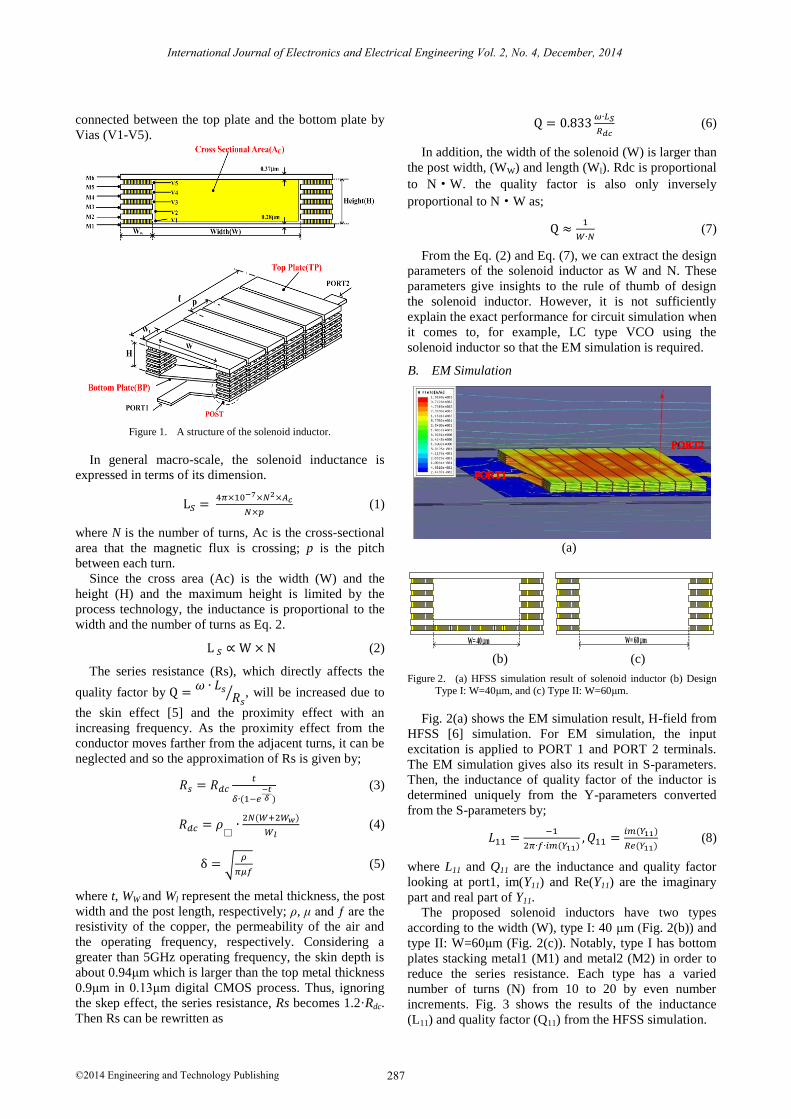
connected between the top plate and the bottom plate by
Vias (V1-V5).
Figure 1. A structure of the solenoid inductor.
In general macro-scale, the solenoid inductance is
expressed in terms of its dimension.
(1)
where N is the number of turns, Ac is the cross-sectional
area that the magnetic flux is crossing; p is the pitch
between each turn.
Since the cross area (Ac) is the width (W) and the
height (H) and the maximum height is limited by the
process technology, the inductance is proportional to the
width and the number of turns as Eq. 2.
(2)
The series resistance (Rs), which directly affects the
quality factor by
⁄ , will be increased due to
the skin effect [5] and the proximity effect with an
increasing frequency. As the proximity effect from the
conductor moves farther from the adjacent turns, it can be
neglected and so the approximation of Rs is given by;
(3)
(4)
√
(5)
where t, WW and Wl represent the metal thickness, the post
width and the post length, respectively; ρ, μ and ƒ are the
resistivity of the copper, the permeability of the air and
the operating frequency, respectively. Considering a
greater than 5GHz operating frequency, the skin depth is
about 0.94μm which is larger than the top metal thickness
0.9μm in 0.13μm digital CMOS process. Thus, ignoring
the skep effect, the series resistance, Rs becomes 1.2·Rdc.
Then Rs can be rewritten as
(6)
In addition, the width of the solenoid (W) is larger than
the post width, (WW) and length (Wl). Rdc is proportional
to N·W. the quality factor is also only inversely
proportional to N·W as;
(7)
From the Eq. (2) and Eq. (7), we can extract the design
parameters of the solenoid inductor as W and N. These
parameters give insights to the rule of thumb of design
the solenoid inductor. However, it is not sufficiently
explain the exact performance for circuit simulation when
it comes to, for example, LC type VCO using the
solenoid inductor so that the EM simulation is required.
B. EM Simulation
(a)
W= 40 μm W= 60 μm
(b) (c)
Figure 2. (a) HFSS simulation result of solenoid inductor (b) Design Type I: W=40μm, and (c) Type II: W=60μm.
Fig. 2(a) shows the EM simulation result, H-field from
HFSS [6] simulation. For EM simulation, the input
excitation is applied to PORT 1 and PORT 2 terminals.
The EM simulation gives also its result in S-parameters.
Then, the inductance of quality factor of the inductor is
determined uniquely from the Y-parameters converted
from the S-parameters by;
(8)
where L11 and Q11 are the inductance and quality factor
looking at port1, im(Y11) and Re(Y11) are the imaginary
part and real part of Y11.
The proposed solenoid inductors have two types
according to the width (W), type I: 40 μm (Fig. 2(b)) and
type II: W=60μm (Fig. 2(c)). Notably, type I has bottom
plates stacking metal1 (M1) and metal2 (M2) in order to
reduce the series resistance. Each type has a varied
number of turns (N) from 10 to 20 by even number
increments. Fig. 3 shows the results of the inductance
(L11) and quality factor (Q11) from the HFSS simulation.
International Journal of Electronics and Electrical Engineering Vol. 2, No. 4, December, 2014
©2014 Engineering and Technology Publishing 287
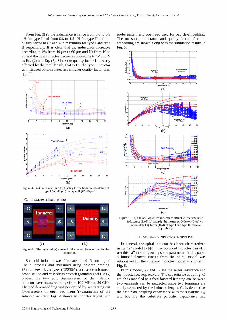
From Fig. 3(a), the inductance is range from 0.6 to 0.9
nH for type I and from 0.8 to 1.5 nH for type II and the
quality factor has 7 and 4 in maximum for type I and type
II respectively. It is clear that the inductance increases
according to Ws from 40 μm to 60 μm and Ns from 10 to
20 and the quality factor decreases according to W and N
as Eq. (2) and Eq. (7). Since the quality factor is directly
affected by the total length, that is Ls, the type I inductor
with stacked bottom plate, has a higher quality factor than
type II.
(a)
(b)
Figure 3. (a) Inductance and (b) Quality factor from the simulation of type I (W=40 μm) and type II (W=60 μm).
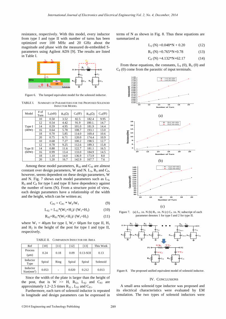
C. Inductor Measurement
(a) ( b)
Figure 4. The layout of (a) solenoid inductor and (b) open pad for de-embedding.
Solenoid inductor was fabricated in 0.13 μm digital
CMOS process and measured using on-chip probing.
With a network analyzer (N5230A), a cascade microtech
probe station and cascade microtech ground-signal (GSG)
probes, the two port S-parameters of the solenoid
inductor were measured range from 100 MHz to 20 GHz.
The pad de-embedding was performed by subtracting out
Y-parameters of open pad from Y-parameters of the
solenoid inductor. Fig. 4 shows an inductor layout with
probe pattern and open pad used for pad de-embedding.
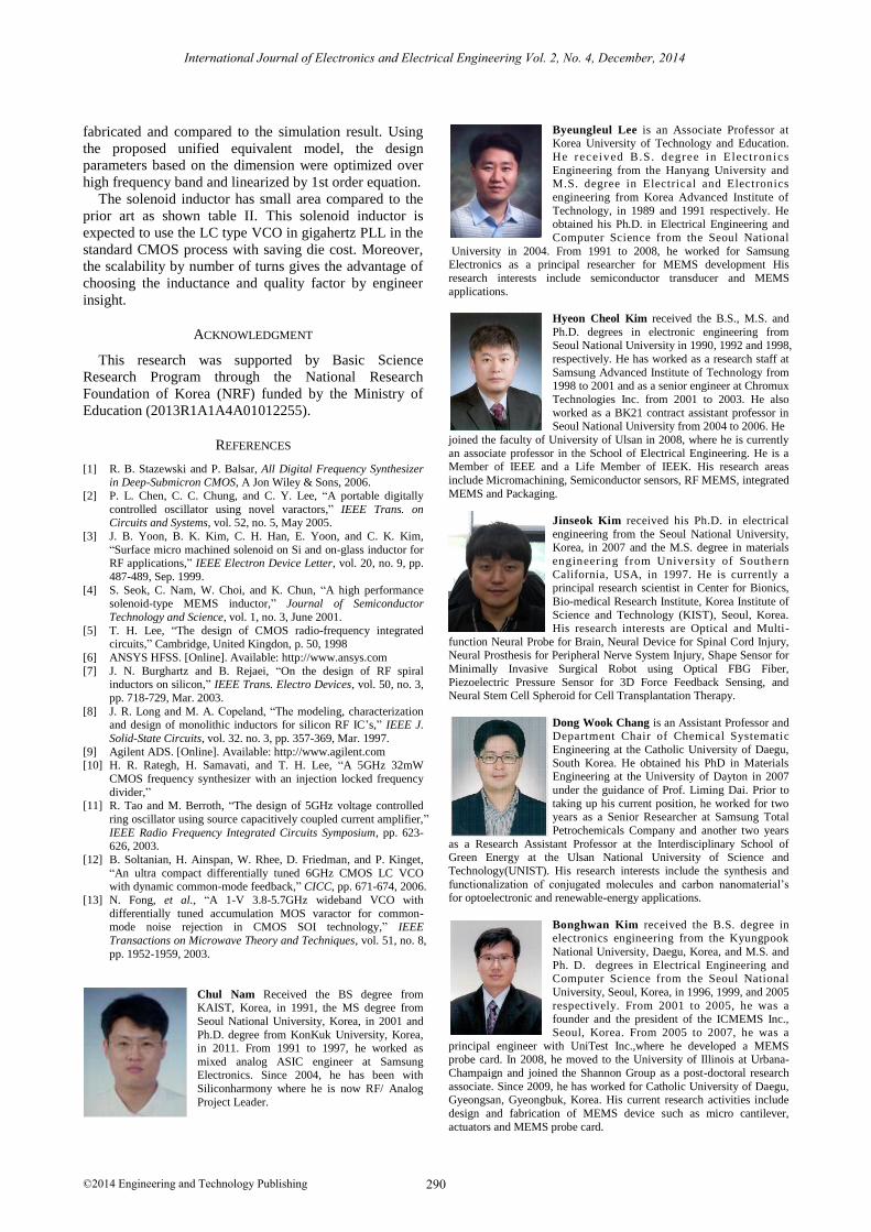
The measured inductance and quality factor after de-
embedding are shown along with the simulation results in
Fig. 5.
(a)
(b)
(c)
(d)
Figure 5. (a) and (c): Measured inductance (Blue) vs. the simulated
inductance (Red) (b) and (d): the measured Q-factor (Blue) vs.
the simulated Q-factor (Red) of type I and type II inductor
respectively.
III. SOLENOID INDUCTOR MODELING
In general, the spiral inductor has been characterized
using “π” model [7]-[8]. The solenoid inductor can also
use this “π” model ignoring some parameter. In this paper,
a lumped-element circuit from the spiral model was
established for the solenoid inductor model as shown in
Fig. 6.
In this model, RS and LS are the series resistance and
the inductance, respectively. The capacitance coupling, Cf
which is modeled as a feed forward fringing one between
two terminals can be neglected since two terminals are
surely separated by the inductor length. CP is denoted as
the base plate coupling capacitance with the substrate. CSI
and RSI are the substrate parasitic capacitance and
0 2 4 6 8 10 12 14 16 18 200
1
2
3
4
5
Frequency(GHz)
Ind
uctan
ce(n
H)
Type II:W=60um
Type I:W=40um
N=10
N=20
N
N=10
N=20
0 2 4 6 8 10 12 14 16 18 200
1
2
3
4
5
6
7
8
Frequency(GHz)
Qu
ality
Fac
to
r
Type I: W=40um
Type II:W=60um
N=10
N=20
N=10
N=20
N
0 2 4 6 8 10 12 14 16 18 200
0.5
1
1.5
2
2.5
3
3.5
4
4.5
5
Frequency(GHz)
Ind
uc
tan
ce(n
H)
Measurement
W=40umSimulation
W=40um
0 2 4 6 8 10 12 14 16 18 200
1
2
3
4
5
6
7
8
Frequency(GHz)Q
ual
ity
Fac
tor
Measurement
W=40um
Simulation
W=40um
International Journal of Electronics and Electrical Engineering Vol. 2, No. 4, December, 2014
©2014 Engineering and Technology Publishing 288
resistance, respectively. With this model, every inductor
from type I and type II with number of turns has been
optimized over 100 MHz and 20 GHz about the
magnitude and phase with the measured de-embedded S-
parameters using Agilent ADS [9]. The results are listed
in Table I.
Figure 6. The lumped equivalent model for the solenoid inductor.
TABLE I. SUMMARY OF PARAMETERS FOR THE PROPOSED SOLENOID
INDUCTOR MODEL
Model # of Turn
LS(nH) RS(Ω) CP(fF) RSI(Ω) CSI(fF)
Type I (40W)
10 0.50 3.52 82.5 182.4 9.95
12 0.54 4.42 91.9 180.1. 14.7
14 0.59 4.95 101.0 181.9 14.4
16 0.64 5.78 108.7 193.1 13.0
18 0.70 5.85 114.0 169.4 10.6
20 0.75 6.71 120.0 174.4 10.9
Type II (60W)
10 0.68 7.27 100.2 198.5 12.7
12 0.78 9.25 112.6 189.3 15.8
14 0.88 11.6 122.7 181.1 16.5
16 0.99 13.4 133.0 184.9 14.5
18 1.10 14.0 136.9 173.9 8.0
20 1.20 16.7 142.9 167.7 7.6
Among these model parameters, RSI and CSI are almost
constant over design parameters, W and N. LS, RS and CP,
however, seems dependent on these design parameters, W
and N. Fig. 7 shows each model parameters such as LS,
RS and CP for type I and type II have dependency against
the number of turns (N). From a structure point of view,
each design parameters have a relationship of the width
and the height, which can be written as;
CP2 = CP1 * W2/W1 (9)
LS2 = LS1*(W2+H2)/ (W1+H1) (10)
RS2=RS1*(W2+H2)/ (W1+H1) (11)
where W1 = 40μm for type I, W2= 60μm for type II, H1
and H2 is the height of the post for type I and type II,
respectively.
TABLE II. COMPARISON INDUCTOR DIE AREA
Ref [10] [11] [12] [13] This Work
Process
(μm) 0.24 0.18 0.09 0.13-SOI 0.13
Inductor
Type Spiral Ring Spiral Spiral Solenoid
Inductor
Size(mm2) 0.053 - 0.020 0.212 0.013
Since the width of the plate is larger than the height of
the post, that is W >> H, RS2, LS2 and CP2 are
approximately 1.2~2.5 times RS1 , LS1 and CP1.
Furthermore, each turn of solenoid inductor is repeated
in longitude and design parameters can be expressed in
terms of N as shown in Fig. 8. Thus these equations are
summarized as
LS (N) =0.048*N + 0.20 (12)
RS (N) =0.765*N+0.78 (13)
CP (N) =4.132*N+62.17 (14)
From these equations, the constants, LS (0), RS (0) and
CP (0) come from the parasitic of input terminals.
10 12 14 16 18 20
0.50
0.55
0.60
0.65
0.70
0.75
0.80
0.85
0.90
0.95
1.00
1.05
1.10
1.15
1.20
1.25
Indu
ctan
ce(n
H)
Number of Turn
Ls1:W=40u
Ls2:W=60u
(a)
10 12 14 16 18 20
4
6
8
10
12
14
16
18
Resi
stan
ce(O
hm)
Number of Turn
Rs1:W=40u
Rs2:W=60u
(b)
10 12 14 16 18 20
80
85
90
95
100
105
110
115
120
125
130
135
140
145
Capa
cita
nce(
fF)
Number of Turn
Cp1:W=40u
Cp2:W=60u
(c)
Figure 7. (a) LS .vs. N (b) RS .vs. N (c) CP .vs. N; subscript of each parameter denotes 1 for type I and 2 for type II.
Figure 8. The proposed unified equivalent model of solenoid inductor.
IV. CONCLUSIONS
A small area solenoid type inductor was proposed and
its electrical characteristics were evaluated by EM
simulation. The two types of solenoid inductors were
International Journal of Electronics and Electrical Engineering Vol. 2, No. 4, December, 2014
©2014 Engineering and Technology Publishing 289
fabricated and compared to the simulation result. Using
the proposed unified equivalent model, the design
parameters based on the dimension were optimized over
high frequency band and linearized by 1st order equation.
The solenoid inductor has small area compared to the
prior art as shown table II. This solenoid inductor is
expected to use the LC type VCO in gigahertz PLL in the
standard CMOS process with saving die cost. Moreover,
the scalability by number of turns gives the advantage of
choosing the inductance and quality factor by engineer
insight.
ACKNOWLEDGMENT
This research was supported by Basic Science
Research Program through the National Research
Foundation of Korea (NRF) funded by the Ministry of
Education (2013R1A1A4A01012255).
REFERENCES
[1] R. B. Stazewski and P. Balsar, All Digital Frequency Synthesizer in Deep-Submicron CMOS, A Jon Wiley & Sons, 2006.
[2] P. L. Chen, C. C. Chung, and C. Y. Lee, “A portable digitally
controlled oscillator using novel varactors,” IEEE Trans. on Circuits and Systems, vol. 52, no. 5, May 2005.
[3] J. B. Yoon, B. K. Kim, C. H. Han, E. Yoon, and C. K. Kim,
“Surface micro machined solenoid on Si and on-glass inductor for RF applications,” IEEE Electron Device Letter, vol. 20, no. 9, pp.
487-489, Sep. 1999.
[4] S. Seok, C. Nam, W. Choi, and K. Chun, “A high performance
solenoid-type MEMS inductor,” Journal of Semiconductor
Technology and Science, vol. 1, no. 3, June 2001.
[5] T. H. Lee, “The design of CMOS radio-frequency integrated circuits,” Cambridge, United Kingdon, p. 50, 1998
[6] ANSYS HFSS. [Online]. Available: http://www.ansys.com
[7] J. N. Burghartz and B. Rejaei, “On the design of RF spiral inductors on silicon,” IEEE Trans. Electro Devices, vol. 50, no. 3,
pp. 718-729, Mar. 2003.
[8] J. R. Long and M. A. Copeland, “The modeling, characterization and design of monolithic inductors for silicon RF IC’s,” IEEE J.
Solid-State Circuits, vol. 32. no. 3, pp. 357-369, Mar. 1997.
[9] Agilent ADS. [Online]. Available: http://www.agilent.com [10] H. R. Rategh, H. Samavati, and T. H. Lee, “A 5GHz 32mW
CMOS frequency synthesizer with an injection locked frequency
divider,” [11] R. Tao and M. Berroth, “The design of 5GHz voltage controlled
ring oscillator using source capacitively coupled current amplifier,”
IEEE Radio Frequency Integrated Circuits Symposium, pp. 623-
626, 2003.
[12] B. Soltanian, H. Ainspan, W. Rhee, D. Friedman, and P. Kinget,
“An ultra compact differentially tuned 6GHz CMOS LC VCO with dynamic common-mode feedback,” CICC, pp. 671-674, 2006.
[13] N. Fong, et al., “A 1-V 3.8-5.7GHz wideband VCO with
differentially tuned accumulation MOS varactor for common-mode noise rejection in CMOS SOI technology,” IEEE
Transactions on Microwave Theory and Techniques, vol. 51, no. 8,
pp. 1952-1959, 2003.
Chul Nam Received the BS degree from KAIST, Korea, in 1991, the MS degree from
Seoul National University, Korea, in 2001 and
Ph.D. degree from KonKuk University, Korea, in 2011. From 1991 to 1997, he worked as
mixed analog ASIC engineer at Samsung Electronics. Since 2004, he has been with
Siliconharmony where he is now RF/ Analog
Project Leader.
Byeungleul Lee is an Associate Professor at Korea University of Technology and Education.
He received B.S. degree in Elec t ron ics
Engineering from the Hanyang University and M.S. degree in Electrical and Electronics
engineering from Korea Advanced Institute of
Technology, in 1989 and 1991 respectively. He obtained his Ph.D. in Electrical Engineering and
Computer Science from the Seoul National
University in 2004. From 1991 to 2008, he worked for Samsung Electronics as a principal researcher for MEMS development His
research interests include semiconductor transducer and MEMS
applications.
Hyeon Cheol Kim received the B.S., M.S. and
Ph.D. degrees in electronic engineering from Seoul National University in 1990, 1992 and 1998,
respectively. He has worked as a research staff at
Samsung Advanced Institute of Technology from 1998 to 2001 and as a senior engineer at Chromux
Technologies Inc. from 2001 to 2003. He also
worked as a BK21 contract assistant professor in Seoul National University from 2004 to 2006. He
joined the faculty of University of Ulsan in 2008, where he is currently
an associate professor in the School of Electrical Engineering. He is a Member of IEEE and a Life Member of IEEK. His research areas
include Micromachining, Semiconductor sensors, RF MEMS, integrated
MEMS and Packaging.
Jinseok Kim received his Ph.D. in electrical
engineering from the Seoul National University, Korea, in 2007 and the M.S. degree in materials
engineering from University of Southern
California, USA, in 1997. He is currently a principal research scientist in Center for Bionics,
Bio-medical Research Institute, Korea Institute of
Science and Technology (KIST), Seoul, Korea. His research interests are Optical and Multi-
function Neural Probe for Brain, Neural Device for Spinal Cord Injury, Neural Prosthesis for Peripheral Nerve System Injury, Shape Sensor for
Minimally Invasive Surgical Robot using Optical FBG Fiber,
Piezoelectric Pressure Sensor for 3D Force Feedback Sensing, and Neural Stem Cell Spheroid for Cell Transplantation Therapy.
Dong Wook Chang is an Assistant Professor and Department Chair of Chemical Systematic
Engineering at the Catholic University of Daegu,
South Korea. He obtained his PhD in Materials Engineering at the University of Dayton in 2007
under the guidance of Prof. Liming Dai. Prior to
taking up his current position, he worked for two years as a Senior Researcher at Samsung Total
Petrochemicals Company and another two years
as a Research Assistant Professor at the Interdisciplinary School of Green Energy at the Ulsan National University of Science and
Technology(UNIST). His research interests include the synthesis and
functionalization of conjugated molecules and carbon nanomaterial’s for optoelectronic and renewable-energy applications.
Bonghwan Kim received the B.S. degree in electronics engineering from the Kyungpook
National University, Daegu, Korea, and M.S. and
Ph. D. degrees in Electrical Engineering and Computer Science from the Seoul National
University, Seoul, Korea, in 1996, 1999, and 2005
respectively. From 2001 to 2005, he was a founder and the president of the ICMEMS Inc.,
Seoul, Korea. From 2005 to 2007, he was a
principal engineer with UniTest Inc.,where he developed a MEMS probe card. In 2008, he moved to the University of Illinois at Urbana-
Champaign and joined the Shannon Group as a post-doctoral research
associate. Since 2009, he has worked for Catholic University of Daegu, Gyeongsan, Gyeongbuk, Korea. His current research activities include
design and fabrication of MEMS device such as micro cantilever,
actuators and MEMS probe card.
International Journal of Electronics and Electrical Engineering Vol. 2, No. 4, December, 2014
©2014 Engineering and Technology Publishing 290

![Solenoid Valves HJE Series€¦ · 4. For double solenoid valve. Air Internal pilot type Not required 0.2~0.7 {2~7.1} [29~102] 1.05 {10.7} [152] 5 2 10 5~50 [41~122] Any](https://static.fdocument.org/doc/165x107/5ea556560f2e8c4b6b6e76a1/solenoid-valves-hje-series-4-for-double-solenoid-valve-air-internal-pilot-type.jpg)


![PHY204 Lecture 29 · 2020-04-02 · PHY204 Lecture 29 [rln29] Inductor and Inductance Inductor (de vice): A wire that is w ound into N tur ns of some shape and area. The current I](https://static.fdocument.org/doc/165x107/5f7ccc378ccd537b2318e733/phy204-lecture-29-2020-04-02-phy204-lecture-29-rln29-inductor-and-inductance.jpg)