Art in Finland, 2010 Semiotics Vesa Matteo Piludu University of Helsinki, semiotic.
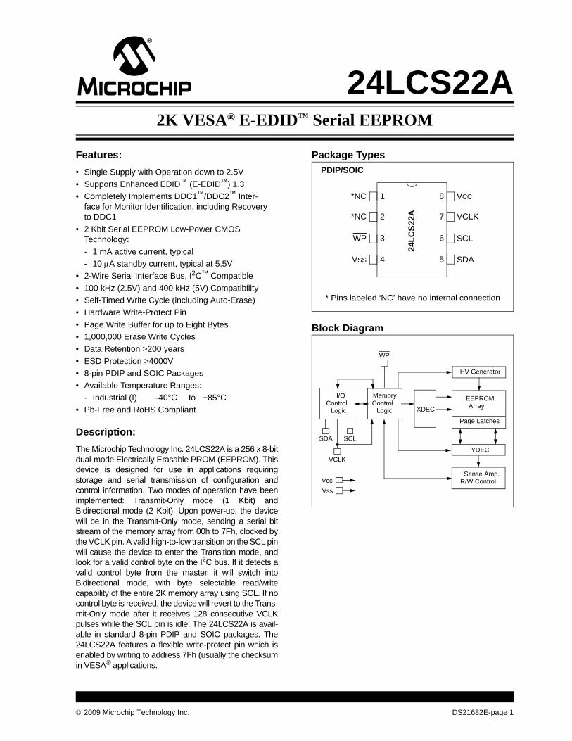
24LCS22A2K VESA® E-EDID™ Serial EEPROM
Features:• Single Supply with Operation down to 2.5V• Supports Enhanced EDID™ (E-EDID™) 1.3• Completely Implements DDC1™/DDC2™ Inter-
face for Monitor Identification, including Recovery to DDC1
• 2 Kbit Serial EEPROM Low-Power CMOS Technology:- 1 mA active current, typical - 10 μA standby current, typical at 5.5V
• 2-Wire Serial Interface Bus, I2C™ Compatible• 100 kHz (2.5V) and 400 kHz (5V) Compatibility• Self-Timed Write Cycle (including Auto-Erase)• Hardware Write-Protect Pin• Page Write Buffer for up to Eight Bytes• 1,000,000 Erase Write Cycles• Data Retention >200 years• ESD Protection >4000V• 8-pin PDIP and SOIC Packages• Available Temperature Ranges:
• Pb-Free and RoHS Compliant
Description:The Microchip Technology Inc. 24LCS22A is a 256 x 8-bitdual-mode Electrically Erasable PROM (EEPROM). Thisdevice is designed for use in applications requiringstorage and serial transmission of configuration andcontrol information. Two modes of operation have beenimplemented: Transmit-Only mode (1 Kbit) andBidirectional mode (2 Kbit). Upon power-up, the devicewill be in the Transmit-Only mode, sending a serial bitstream of the memory array from 00h to 7Fh, clocked bythe VCLK pin. A valid high-to-low transition on the SCL pinwill cause the device to enter the Transition mode, andlook for a valid control byte on the I2C bus. If it detects avalid control byte from the master, it will switch intoBidirectional mode, with byte selectable read/writecapability of the entire 2K memory array using SCL. If nocontrol byte is received, the device will revert to the Trans-mit-Only mode after it receives 128 consecutive VCLKpulses while the SCL pin is idle. The 24LCS22A is avail-able in standard 8-pin PDIP and SOIC packages. The24LCS22A features a flexible write-protect pin which isenabled by writing to address 7Fh (usually the checksumin VESA® applications.
Package Types
Block Diagram
- Industrial (I) -40°C to +85°C
PDIP/SOIC
24LC
S22A
*NC
*NC
WP
VSS
1
2
3
4
8
7
6
5
VCC
VCLK
SCL
SDA
* Pins labeled ‘NC’ have no internal connection
HV Generator
EEPROM Array
Page Latches
YDEC
XDEC
Sense Amp.R/W Control
MemoryControl
Logic
I/OControl
Logic
WP
SDA SCL
VccVss
VCLK
© 2009 Microchip Technology Inc. DS21682E-page 1
24LCS22A
1.0 ELECTRICAL CHARACTERISTICS
Absolute Maximum Ratings(†)
VCC.............................................................................................................................................................................7.0V
All inputs and outputs w.r.t. VSS ......................................................................................................... -0.6V to VCC +1.0V
Storage temperature ...............................................................................................................................-65°C to +150°C
Ambient temperature with power applied................................................................................................-40°C to +125°C
ESD protection on all pins ......................................................................................................................................................≥ 4 kV
TABLE 1-1: DC CHARACTERISTICS
† Notice: Stresses above those listed under “Absolute Maximum Ratings” may cause permanent damage to the device. This is a stress rating only and functional operation of the device at those or any other conditions above those indicated in the operational listings of this specification is not implied. Exposure to maximum rating conditions for extended periods may affect device reliability.
DC CHARACTERISTICS Vcc = +2.5V to 5.5VIndustrial (I): TA = -40°C to +85°C
Param. No. Sym Characteristic Min. Max. Units Test Conditions
SCL and SDA pins:D1 VIH High-level input voltage 0.7 VCC — VD2 VIL Low-level input voltage — 0.3 VCC VInput levels on VCLK pin:D3 VIH High-level input voltage 2.0 — V VCC ≥ 2.7V (Note)D4 VIL Low-level input voltage — 0.2 VCC V VCC ≤ 2.7V (Note)D5 VHYS Hysteresis of Schmitt Trigger
Inputs.05 VCC — V (Note)
D6 VOL1 Low-level output voltage — 0.4 V IOL = 3 mA, VCC = 2.5V (Note)D7 VOL2 Low-level output voltage — 0.6 V IOL = 6 mA, VCC = 2.5VD8 ILI Input leakage current — ±1 μA VIN = 0.1V to VCC
D9 ILO Output leakage current — ±1 μA VOUT = 0.1V to VCC
D10 CIN, COUT Pin capacitance(all inputs/outputs)
— 10 pF VCC = 5.0V (Note)TA = 25°C, FCLK = 1 MHz
Operating current:D10 ICC WRITE Operating current — 3 mA VCC = 5.5V,D11 ICC READ Operating current — 1 mA VCC = 5.5V, SCL = 400 kHzD12 ICCS Standby current —
—30
100μAμA
VCC = 3.0V, SDA = SCL = VCCVCC = 5.5V, SDA = SCL = VCCVCLK = VSS
Note: This parameter is periodically sampled and not 100% tested.
DS21682E-page 2 © 2009 Microchip Technology Inc.

24LCS22A
TABLE 1-2: AC CHARACTERISTICSAC CHARACTERISTICS Vcc = +2.5V to 5.5VIndustrial (I): TA = -40°C to +85°C
Param. No. Sym Parameter Min Max Units Conditions
1 FCLK Clock frequency ——
100400
kHz 2.5V ≤ VCC ≤ 5.5V4.5V ≤ VCC ≤ 5.5V
2 THIGH Clock high time 4000600
——
ns 2.5V ≤ VCC ≤ 5.5V4.5V ≤ VCC ≤ 5.5V
3 TLOW Clock low time 47001300
——
ns 2.5V ≤ VCC ≤ 5.5V4.5V ≤ VCC ≤ 5.5V
4 TR SDA and SCL rise time ——
1000300
ns 2.5V ≤ VCC ≤ 5.5V (Note 1)4.5V ≤ VCC ≤ 5.5V (Note 1)
5 TF SDA and SCL fall time ——
300300
ns (Note 1)
6 THD:STA Start condition hold time 4000600
——
ns 2.5V ≤ VCC ≤ 5.5V4.5V ≤ VCC ≤ 5.5V
7 TSU:STA Start condition setup time 4700600
——
ns 2.5V ≤ VCC ≤ 5.5V4.5V ≤ VCC ≤ 5.5V
8 THD:DAT Data input hold time 00
——
ns (Note 2)
9 TSU:DAT Data input setup time 250100
——
ns 2.5V ≤ VCC ≤ 5.5V4.5V ≤ VCC ≤ 5.5V
10 TSU:STO Stop condition setup time 4000600
——
ns 2.5V ≤ VCC ≤ 5.5V4.5V ≤ VCC ≤ 5.5V
11 TAA Output valid from clock(Note 2)
——
3500900
ns 2.5V ≤ VCC ≤ 5.5V4.5V ≤ VCC ≤ 5.5V
12 TBUF Bus free time: Time the bus must be free before a new transmission can start
47001300
——
ns 2.5V ≤ VCC ≤ 5.5V4.5V ≤ VCC ≤ 5.5V
13 TOF Output fall time from VIHminimum to VIL maximum
—20+0.1CB
250250
ns 2.5V ≤ VCC ≤ 5.5V (Note 1)4.5V ≤ VCC ≤ 5.5V (Note 1)
14 TSP Input filter spike suppression(SDA and SCL pins)
——
5050
ns (Notes 1 and 3)
15 TWR Write cycle time (byte or page) ——
1010
ms
16 TVAA Output valid from VCLK ——
20001000
ns
17 TVHIGH VCLK high time 4000600
——
ns
18 TVLOW VCLK low time 47001300
——
ns
19 TVHST VCLK setup time 00
——
ns
20 TSPVL VCLK hold time 4000600
——
ns
21 TVHZ Mode transition time ——
1000500
ns
22 TVPU Transmit-only power-up time 00
——
ns
23 TSPV Input filter spike suppression (VCLK pin)
——
100100
ns
24 — Endurance 1M — cycles 25°C, VCC = 5.0V, Block mode (Note 4)
Note 1: Not 100% tested. CB = total capacitance of one bus line in pF.2: As a transmitter, the device must provide an internal minimum delay time to bridge the undefined region (minimum 300 ns) of the
falling edge of SCL to avoid unintended generation of Start or Stop conditions.3: The combined TSP and VHYS specifications are due to Schmitt Trigger inputs which provide improved noise spike suppression.
This eliminates the need for a TI specification for standard operation.4: This parameter is not tested but established by characterization. For endurance estimates in a specific application, please consult
the Total Endurance™ Model which can be obtained from Microchip’s web site at www.microchip.com.
© 2009 Microchip Technology Inc. DS21682E-page 3

24LCS22A
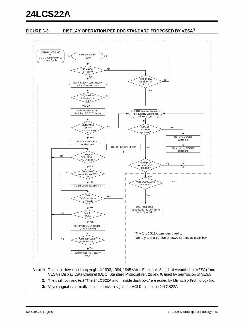
2.0 FUNCTIONAL DESCRIPTIONThe 24LCS22A is designed to comply to the DDCStandard proposed by VESA (Figure 3-3) with theexception that it is not Access.bus™ capable. It oper-ates in two modes, the Transmit-Only mode (1 Kbit)and the Bidirectional mode (2 Kbit). There is a separate2-wire protocol to support each mode, each having aseparate clock input but sharing a common data line(SDA). The device enters the Transmit-Only modeupon power-up. In this mode, the device transmits databits on the SDA pin in response to a clock signal on theVCLK pin. The device will remain in this mode until avalid high-to-low transition is placed on the SCL input.When a valid transition on SCL is recognized, thedevice will switch into the Bidirectional mode and lookfor its control byte to be sent by the master. If it detectsits control byte, it will stay in the Bidirectional mode.Otherwise, it will revert to the Transmit-Only mode afterit sees 128 VCLK pulses.
2.1 Transmit-Only ModeThe device will power up in the Transmit-Only mode ataddress 00h. This mode supports a unidirectional2-wire protocol for continuous transmission of the first1 Kbit of the memory array. This device requires that it
be initialized prior to valid data being sent in the Trans-mit-Only mode (Section 2.2 “Initialization Proce-dure”). In this mode, data is transmitted on the SDApin in 8-bit bytes, with each byte followed by a ninth,Null bit (Figure 2-1). The clock source for the Transmit-Only mode is provided on the VCLK pin, and a data bitis output on the rising edge on this pin. The eight bits ineach byte are transmitted Most Significant bit first.Each byte within the memory array will be output insequence. After address 7Fh in the memory array istransmitted, the internal Address Pointers will wraparound to the first memory location (00h) and continue.The Bidirectional mode clock (SCL) pin must be heldhigh for the device to remain in the Transmit-Onlymode.
2.2 Initialization ProcedureAfter VCC has stabilized, the device will be in the Trans-mit-Only mode. Nine clock cycles on the VCLK pinmust be given to the device for it to perform internalsychronization. During this period, the SDA pin will bein a high-impedance state. On the rising edge of thetenth clock cycle, the device will output the first validdata bit which will be the Most Significant bit in address00h. (Figure 2-2).
FIGURE 2-1: TRANSMIT-ONLY MODE
FIGURE 2-2: DEVICE INITIALIZATION
SCL
SDA
VCLK
TVAA TVAA
Bit 1 (LSB)Null Bit
Bit 1 (MSB) Bit 7
TVLOWTVHIGH
TVAA TVAA
Bit 8 Bit 7High-impedance for 9 clock cyclesTVPU
1 2 8 9 10 11
SCL
SDA
VCLK
VCC
DS21682E-page 4 © 2009 Microchip Technology Inc.

24LCS22A
3.0 BIDIRECTIONAL MODEBefore the 24LCS22A can be switched into theBidirectional mode (Figure 3-1), it must enter theTransition mode, which is done by applying a validhigh-to-low transition on the Bidirectional mode clock(SCL). As soon as it enters the Transition mode, it looksfor a control byte ‘1010 000X’ on the I2C™ bus, andstarts to count pulses on VCLK. Any high-to-lowtransition on the SCL line will reset the count. If it seesa pulse count of 128 on VCLK while the SCL line is idle,it will revert back to the Transmit-Only mode, andtransmit its contents starting with the Most Significantbit in address 00h. However, if it detects the controlbyte on the I2C bus (Figure 3-2), it will switch to theBidirectional mode. Once the device has made thetransition to the Bidirectional mode, the only way toswitch the device back to the Transmit-Only mode is toremove power from the device. The mode transitionprocess is shown in detail in Figure 3-3.
Once the device has switched into the Bidirectionalmode, the VCLK input is disregarded, with theexception that a logic high level is required to enablewrite capability. In Bidirectional mode the user hasaccess to the entire 2K array, whereas in the Transmit-Only mode, the user can only access the first 1K. Thismode supports a two-wire bidirectional datatransmission protocol (I2C). In this protocol, a devicethat sends data on the bus is defined to be thetransmitter, and a device that receives data from thebus is defined to be the receiver. The bus must becontrolled by a master device that generates theBidirectional mode clock (SCL), controls access to thebus and generates the Start and Stop conditions, whilethe 24LCS22A acts as the slave. Both master andslave can operate as transmitter or receiver, but themaster device determines which mode is activated. Inthe Bidirectional mode, the 24LCS22A only respondsto commands for device ‘1010 000X’.
FIGURE 3-1: MODE TRANSITION WITH RECOVERY TO TRANSMIT-ONLY MODE
FIGURE 3-2: SUCCESSFUL MODE TRANSITION TO BIDIRECTIONAL MODE
TVHZ
SCL
SDA
VCLK
Transmit-OnlyMODE Bidirectional Recovery to Transmit-Only mode
Bit8(MSB of data in 00h)
VCLK count = 1 2 3 4 127 128
Transition mode with possibility to return to Transmit-Only modeBidirectionalpermanently
SCL
SDAVCLK count = 1 2 n 0
VCLK
Transmit-OnlyMODE
S 1 0 1 0 00 0 0 ACK
n < 128
© 2009 Microchip Technology Inc. DS21682E-page 5
24LCS22A
FIGURE 3-3: DISPLAY OPERATION PER DDC STANDARD PROPOSED BY VESA®Communicationis idle
Is Vsyncpresent?
No
Send EDID™ continuouslyusing Vsync as clock
High-to-lowtransition on
SCL?
No
Yes
Yes
Stop sending EDID.Switch to DDC2™ mode.
Display has
transition state?
optional
Set Vsync counter = 0
Change on
VCLK lines?SCL, SDA orNo
Yes
High-lowtransition on SCL
?
Reset Vsync counter = 0
No
Yes
Valid
received?DDC2 address
No
No VCLK cycle?
YesIncrement VCLK counter
Yes
Switch back to DDC1™mode.
DDC2 communicationidle. Display waiting for
address byte.
DDC2Baddress
received?
Yes
Receive DDC2Bcommand
Respond to DDC2Bcommand
Is displayAccess.bus™
Yes
Valid Access.busaddress?
No
Yes
See Access.busspecification to determine
correct procedure.
Yes
No
Yes
No
No
No
The 24LCS22A was designed to
Display Power-onor
DDC Circuit Poweredfrom +5 volts
or start timerReset counter or timer
(if appropriate)
Counter=128 ortimer expired?
High-to-lowtransition on
SCL?
No
Yes
comply to the portion of flowchart inside dash box
Note 1: The base flowchart is copyright © 1993, 1994, 1995 Video Electronic Standard Association (VESA) fromVESA’s Display Data Channel (DDC) Standard Proposal ver. 2p rev. 0, used by permission of VESA.
2: The dash box and text “The 24LCS22A and... inside dash box.” are added by Microchip Technology Inc.
3: Vsync signal is normally used to derive a signal for VCLK pin on the 24LCS22A.
capable?
DS21682E-page 6 © 2009 Microchip Technology Inc.

24LCS22A
3.1 Bidirectional Mode BusCharacteristicsThe following bus protocol has been defined:
• Data transfer may be initiated only when the bus is not busy
• During data transfer, the data line must remain stable whenever the clock line is high. Changes in the data line while the clock line is high will be interpreted as a Start or Stop condition
Accordingly, the following bus conditions have beendefined (Figure 3-4).
3.1.1 BUS NOT BUSY (A)Both data and clock lines remain high.
3.1.2 START DATA TRANSFER (B)A high-to-low transition of the SDA line while the clock(SCL) is high determines a Start condition. Allcommands must be preceded by a Start condition.
3.1.3 STOP DATA TRANSFER (C)A low-to-high transition of the SDA line while the clock(SCL) is high determines a Stop condition. Alloperations must be ended with a Stop condition.
3.1.4 DATA VALID (D)The state of the data line represents valid data when,after a Start condition, the data line is stable for theduration of the high period of the clock signal.
The data on the line must be changed during the lowperiod of the clock signal. There is one clock pulse perbit of data.
Each data transfer is initiated with a Start condition andterminated with a Stop condition. The number of thedata bytes transferred between the Start and Stopconditions is determined by the master device and istheoretically unlimited, although only the last eight willbe stored when doing a write operation. When anoverwrite does occur it will replace data in a first-in first-out (FIFO) fashion.
3.1.5 ACKNOWLEDGEEach receiving device, when addressed, is obliged togenerate an acknowledge after the reception of eachbyte. The master device must generate an extra clockpulse which is associated with this Acknowledge bit.
The device that acknowledges has to pull down theSDA line during the Acknowledge clock pulse in such away that the SDA line is stable low during the highperiod of the acknowledge related clock pulse. Ofcourse, setup and hold times must be taken intoaccount. A master must signal an end of data to theslave by not generating an Acknowledge bit on the lastbyte that has been clocked out of the slave. In thiscase, the slave must leave the data line high to enablethe master to generate the Stop condition.
FIGURE 3-4: DATA TRANSFER SEQUENCE ON THE SERIAL BUS
Note: Once switched into Bidirectional mode, the24LCS22A will remain in that mode untilpower is removed. Removing power is theonly way to reset the 24LCS22A into theTransmit-Only mode.
Note: The 24LCS22A does not generate anyAcknowledge bits if an internalprogramming cycle is in progress.
(A) (B) (D) (D) (A)(C)
StartCondition
Address orAcknowledge
Valid
DataAllowed
to Change
StopCondition
SCL
SDA
© 2009 Microchip Technology Inc. DS21682E-page 7

24LCS22A
FIGURE 3-5: BUS TIMING START/STOPFIGURE 3-6: BUS TIMING DATA
3.1.6 SLAVE ADDRESSAfter generating a Start condition, the bus mastertransmits the slave address consisting of a 7-bit devicecode (1010000) for the 24LCS22A.
The eighth bit of slave address determines whether themaster device wants to read or write to the 24LCS22A(Figure 3-7).
The 24LCS22A monitors the bus for its correspondingslave address continuously. It generates anAcknowledge bit if the slave address was true and it isnot in a Programming mode.
FIGURE 3-7: CONTROL BYTE ALLOCATION
SCL
SDA
Start Stop
VHYSTSU:STOTHD:STA
TSU:STA
SCL
SDAIN
SDAOUT
TSU:STA
TSP
TAA
TF
TLOW
THIGH
THD:STA
THD:DAT TSU:DAT TSU:STO
TBUFTAA
TR
Operation Slave Address R/WRead 1010000 1
Write 1010000 0
R/W A
1 0 1 0 0 0 0
Read/WriteStart
Slave Address
DS21682E-page 8 © 2009 Microchip Technology Inc.
24LCS22A
4.0 WRITE OPERATION
4.1 Byte WriteFollowing the Start signal from the master, the slaveaddress (four bits), three zero bits (000) and the R/Wbit which is a logic low are placed onto the bus by themaster transmitter. This indicates to the addressedslave receiver that a byte with a word address willfollow after it has generated an Acknowledge bit duringthe ninth clock cycle. Therefore, the next bytetransmitted by the master is the word address and willbe written into the Address Pointer of the 24LCS22A.After receiving another Acknowledge signal from the24LCS22A the master device will transmit the dataword to be written into the addressed memory location.The 24LCS22A acknowledges again and the mastergenerates a Stop condition. This initiates the internalwrite cycle, and during this time the 24LCS22A will notgenerate Acknowledge signals (Figure 4-1).
It is required that VCLK be held at a logic high levelduring command and data transfer in order to programthe device. This applies to both byte write and pagewrite operation. Note, however, that the VCLK isignored during the self-timed program operation.Changing VCLK from high-to-low during the self-timedprogram operation will not halt programming of thedevice.
4.2 Page Write The write control byte, word address and the first databyte are transmitted to the 24LCS22A in the same wayas in a byte write. But instead of generating a Stopcondition the master transmits up to eight data bytes tothe 24LCS22A which are temporarily stored in the on-chip page buffer and will be written into the memoryafter the master has transmitted a Stop condition. Afterthe receipt of each word, the three lower order AddressPointer bits are internally incremented by one. Thehigher order five bits of the word address remainsconstant. If the master should transmit more than eightwords prior to generating the Stop condition, theaddress counter will roll over and the previouslyreceived data will be overwritten. As with the byte writeoperation, once the Stop condition is received aninternal write cycle will begin (Figure 5-2).
It is required that VCLK be held at a logic high levelduring command and data transfer in order to programthe device. This applies to both byte write and pagewrite operation. Note, however, that the VCLK isignored during the self-timed program operation.Changing VCLK from high-to-low during the self-timedprogram operation will not halt programming of thedevice.
Note: Page write operations are limited to writingbytes within a single physical page,regardless of the number of bytes actuallybeing written. Physical page boundariesstart at addresses that are integermultiples of the page buffer size (or ‘pagesize’) and end at addresses that areinteger multiples of [page size – 1]. If aPage Write command attempts to writeacross a physical page boundary, theresult is that the data wraps around to thebeginning of the current page (overwritingdata previously stored there), instead ofbeing written to the next page as might beexpected. It is therefore necessary for theapplication software to prevent page writeoperations that would attempt to cross apage boundary.
© 2009 Microchip Technology Inc. DS21682E-page 9

24LCS22A
FIGURE 4-1: BYTE WRITEFIGURE 4-2: VCLK WRITE ENABLE TIMING
Bus ActivityMaster
SDA Line
Bus Activity
ControlByte
WordAddress Data
STOP
START
ACK
S P
ACK
ACK
VCLK
SCL
SDAIN
VCLK
THD:STA TSU:STO
TVHST TSPVL
DS21682E-page 10 © 2009 Microchip Technology Inc.

24LCS22A
5.0 ACKNOWLEDGE POLLINGSince the device will not acknowledge during a writecycle, this can be used to determine when the cycle iscomplete (this feature can be used to maximize busthroughput). Once the Stop condition for a Writecommand has been issued from the master, the deviceinitiates the internally timed write cycle. ACK pollingcan be initiated immediately. This involves the mastersending a Start condition followed by the control bytefor a Write command (R/W = 0). If the device is stillbusy with the write cycle, then no ACK will be returned.If the cycle is complete, then the device will return theACK and the master can then proceed with the nextRead or Write command. See Figure 5-1 for the flowdiagram.
FIGURE 5-1: ACKNOWLEDGE POLLING FLOW
FIGURE 5-2: PAGE WRITE
Did DeviceAcknowledge(ACK = 0)?
SendWrite Command
Send StopCondition to
Initiate Write Cycle
Send Start
Send Control Bytewith R/W = 0
NextOperation
No
Yes
SDA Line
ControlByte
WordAddress
STOP
START
ACK
ACK
ACK
ACK
ACK
Data n + 1 Data n + 7Data (n)
PS
VCLK
Bus ActivityMaster
Bus Activity
© 2009 Microchip Technology Inc. DS21682E-page 11
24LCS22A
6.0 WRITE PROTECTIONWhen using the 24LCS22A in the Bidirectional mode,the VCLK pin can be used as a write-protect controlpin. Setting VCLK high allows normal write operations,while setting VCLK low prevents writing to any locationin the array. Connecting the VCLK pin to VSS wouldallow the 24LCS22A to operate as a serial ROM,although this configuration would prevent using thedevice in the Transmit-Only mode.
Additionally, pin 3 performs a flexible write-protectfunction. The 24LCS22A contains a write protectioncontrol fuse whose factory default state is cleared.Writing any data to address 7Fh (normally thechecksum in DDC applications) sets the fuse whichenables the WP pin. Until this fuse is set, the24LCS22A is always write enabled (if VCLK = 1). Afterthe fuse is set, the write capability of the 24LCS22A isdetermined by both VCLK and WP pins (Table 6-1).
TABLE 6-1: WRITE-PROTECT TRUTH TABLE
7.0 READ OPERATIONRead operations are initiated in the same way as writeoperations with the exception that the R/W bit of theslave address is set to one. There are three basic typesof read operations: current address read, random readand sequential read.
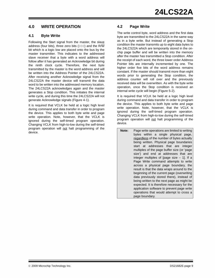
7.1 Current Address ReadThe 24LCS22A contains an address counter thatmaintains the address of the last word accessed,internally incremented by one. Therefore, if theprevious access (either a read or write operation) wasto address n, the next current address read operationwould access data from address n + 1. Upon receipt ofthe slave address with R/W bit set to one, the24LCS22A issues an acknowledge and transmits theeight bit data word. The master will not acknowledgethe transfer, but does generate a Stop condition and the24LCS22A discontinues transmission (Figure 7-1).
FIGURE 7-1: CURRENT ADDRESS READ
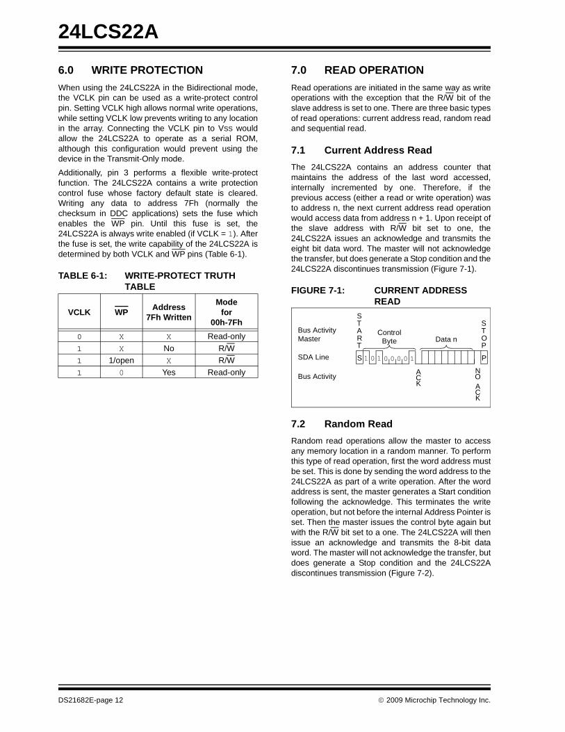
7.2 Random ReadRandom read operations allow the master to accessany memory location in a random manner. To performthis type of read operation, first the word address mustbe set. This is done by sending the word address to the24LCS22A as part of a write operation. After the wordaddress is sent, the master generates a Start conditionfollowing the acknowledge. This terminates the writeoperation, but not before the internal Address Pointer isset. Then the master issues the control byte again butwith the R/W bit set to a one. The 24LCS22A will thenissue an acknowledge and transmits the 8-bit dataword. The master will not acknowledge the transfer, butdoes generate a Stop condition and the 24LCS22Adiscontinues transmission (Figure 7-2).
VCLK WP Address 7Fh Written
Modefor
00h-7Fh0 X X Read-only1 X No R/W1 1/open X R/W1 0 Yes Read-only
Control
ACK
S P
Byte Data nBus Activity
SDA Line
Bus ActivityACK
NO
Master
1 0 1 0 0 0 0 1
STOP
START
DS21682E-page 12 © 2009 Microchip Technology Inc.
24LCS22A
FIGURE 7-2: RANDOM READFIGURE 7-3: SEQUENTIAL READ
7.3 Sequential ReadSequential reads are initiated in the same way as arandom read except that after the 24LCS22A transmitsthe first data byte, the master issues an acknowledgeas opposed to a Stop condition in a random read. Thisdirects the 24LCS22A to transmit the next sequentiallyaddressed 8-bit word (Figure 7-3).
To provide sequential reads the 24LCS22A contains aninternal Address Pointer which is incremented by oneat the completion of each operation. This AddressPointer allows the entire memory contents to be seriallyread during one operation.
7.4 Noise ProtectionThe 24LCS22A employs a VCC threshold detectorcircuit which disables the internal erase/write logic if theVCC is below 1.5 volts at nominal conditions.
The SDA, SCL and VCLK inputs have Schmitt Triggerand filter circuits which suppress noise spikes to assureproper device operation even on a noisy bus.
Bus ActivityMaster
SDA Line
Bus Activity
ControlByte
WordAddress Data n
ACK
START
NO
STAR Control
Byte
ACK
ACK
S S
T
P
STOP
1 0 1 0 0 0 0 0 00000 111
ACK
ACK
P
Bus ActivityMaster
SDA Line
Bus Activity
ControlByte
Data n Data n + 1 Data n + 2 Data n + x
ACK
ACK
ACK
NO
ACK
STOP
© 2009 Microchip Technology Inc. DS21682E-page 13

24LCS22A
8.0 PIN DESCRIPTIONSThe descriptions of the pins are listed in Table 8-1.
TABLE 8-1: PIN FUNCTION TABLE
8.1 Write-Protect (WP)This pin is used for flexible write protection of the24LCS22A. When memory location 7Fh is written withany data, this pin is enabled and determines the writecapability of the 24LCS22A (Table 6-1).
8.2 Serial Address/Data Input/Output (SDA)
This pin is used to transfer addresses and data into andout of the device, when the device is in the Bidirectionalmode. In the Transmit-Only mode, which only allowsdata to be read from the device, data is also transferredon the SDA pin. This pin is an open drain terminal,therefore the SDA bus requires a pull-up resistor toVCC (typical 10 kΩ for 100 kHz, 2 kΩ for 400 kHz).
For normal data transfer in the Bidirectional mode, SDAis allowed to change only during SCL low. Changesduring SCL high are reserved for indicating the Startand Stop conditions.
8.3 Serial Clock (SCL)This pin is the clock input for the Bidirectional mode,and is used to synchronize data transfer to and from thedevice. It is also used as the signaling input to switchthe device from the Transmit-Only mode to theBidirectional mode. It must remain high for the chip tocontinue operation in the Transmit-Only mode.
8.4 Serial Clock (VCLK)This pin is the clock input for the Transmit-Only mode(DDC1). In the Transmit-Only mode, each bit is clockedout on the rising edge of this signal. In the Bidirectionalmode, a high logic level is required on this pin to enablewrite capability.
Name Function
WP Write-Protect (active low)
VSS Ground
SDA Serial Address/Data I/O
SCL Serial Clock (Bidirectional mode)
VCLK Serial Clock (Transmit-Only mode)
VCC +2.5V to 5.5V Power Supply
NC No Internal Connection
DS21682E-page 14 © 2009 Microchip Technology Inc.
24LCS22A
9.0 PACKAGING INFORMATION
9.1 Package Marking Information
XXXXXXXXTXX NNN
YYWW
8-Lead PDIP (300 mil) Example:
24LCS22AI/P NNN
0145
8-Lead SOIC (3.90 mm) Example:
* Standard marking consists of Microchip part number, year code, week code, traceability code (facilitycode, mask rev#, and assembly code).
XXXXXXXTXX YYWW
NNN
4LCS22AISN 0145
NNN
Legend: XX...X Part number or part number codeT Temperature (I, E)Y Year code (last digit of calendar year)YY Year code (last 2 digits of calendar year)WW Week code (week of January 1 is week ‘01’)NNN Alphanumeric traceability code (2 characters for small packages)
Pb-free JEDEC designator for Matte Tin (Sn)
Note: For very small packages with no room for the Pb-free JEDEC designator , the marking will only appear on the outer carton or reel label.
Note: In the event the full Microchip part number cannot be marked on one line, it willbe carried over to the next line, thus limiting the number of availablecharacters for customer-specific information.
3e
3e
3e
3e
3e
3e
© 2009 Microchip Technology Inc. DS21682E-page 15

24LCS22A
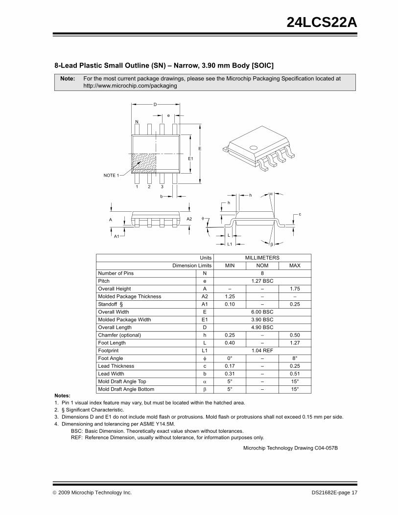
���������� ���������� ������������� ����������
�������� ������ �!"�����#�$�%��&"��'��� ��(�)"&�'"!&�)�����&�#�*�&��&�����&���#������� +������%����&�,����&��!&���-� ��'��!��!�����#�.��#��&�����"#��'�#�%��!����&"!��!����#�%��!����&"!��!�!������&��$���#�����/����!�#���� ��'��!��������#�&���������������.�0������
1�,2�1�!�����'��!���� ���&��������$��&� ��"��!�*��*�&�"&�&������!�
����� 3�&���'!&��"��&����4����#�*���!(�����!��!���&��������������4�����������%���&������&�#��&��&&�255***�'��������'5���4�����
6��&! �7,8.���'��!���9�'�&! ��7 7:� ��;
7"')��%����! 7 <��&�� � �����1�, ��&����&��������� � = = ������#�#����4���� ���4��!! �� ���� ��-� ����1�!��&����&��������� �� ���� = =��"�#��&���"�#��>�#&� . ���� �-�� �-����#�#����4����>�#&� .� ���� ���� ��<�: �����9���&� � �-�< �-?� ���� ���&����&��������� 9 ���� ��-� ����9��#� ���4��!! � ���< ���� ����6����9��#�>�#&� )� ���� ��?� ����9*��9��#�>�#&� ) ���� ���< ����: ������*����������+ �1 = = ��-�
N
E1
NOTE 1
D
1 2 3
A
A1
A2
L
b1b
e
E
eB
c
������� ������� ��*��� ,�����<1
DS21682E-page 16 © 2009 Microchip Technology Inc.
24LCS22A
���������� �� ���!�� ���� �������""�#$��%&����������� !�'�
�������� ������ �!"�����#�$�%��&"��'��� ��(�)"&�'"!&�)�����&�#�*�&����&�����&���#������� +������%����&�,����&��!&���-� ��'��!��!�����#�.��#��&�����"#��'�#�%��!����&"!��!����#�%��!����&"!��!�!������&��$���#������''����!�#���� ��'��!��������#�&���������������.�0������
1�,2 1�!�����'��!���� ���&��������$��&� ��"��!�*��*�&�"&�&������!��.32 ��%��������'��!��(�"!"�����*�&�"&�&������(�%���%'�&����"�!�!�����
����� 3�&���'!&��"��&����4����#�*���!(�����!��!���&��������������4�����������%���&������&�#��&��&&�255***�'��������'5���4�����
6��&! ��99��. .����'��!���9�'�&! ��7 7:� ��;
7"')��%����! 7 <��&�� � �����1�,: �����8����& � = = ������#�#����4���� ���4��!! �� ���� = =�&��#%%��+ �� ���� = ����: �����>�#&� . ?����1�,��#�#����4����>�#&� .� -����1�,: �����9���&� � �����1�,,��'%��@�&����A � ���� = ����3&�9���&� 9 ���� = ����3&���& 9� ������.33&������ � �B = <B9��#� ���4��!! � ���� = ����9��#�>�#&� ) ��-� = ������#���%&������� � � �B = ��B��#���%&�������1&&' � �B = ��B
D
Ne
E
E1
NOTE 1
1 2 3
b
A
A1
A2
L
L1
c
h
h
φ
β
α
������� ������� ��*��� ,������1
© 2009 Microchip Technology Inc. DS21682E-page 17

24LCS22A
���������� �� ���!�� ���� �������""�#$��%&����������� !�'�
����� 3�&���'!&��"��&����4����#�*���!(�����!��!���&��������������4�����������%���&������&�#��&��&&�255***�'��������'5���4�����
DS21682E-page 18 © 2009 Microchip Technology Inc.
24LCS22A
APPENDIX A: REVISION HISTORY
Revision BCorrections to Section 1.0, Electrical Characteristics.
Revision CRevised Section 8.1. Added new package legend.
Revision D (07/2008)Revised Features (added Pb-free); Replaced PackageDrawings (Rev. AP); Revised Product ID System.
Revision E (06/2009)Revised Package Marking examples.
© 2009 Microchip Technology Inc. DS21682E-page 19

24LCS22A
NOTES:DS21682E-page 20 © 2009 Microchip Technology Inc.
24LCS22A
THE MICROCHIP WEB SITEMicrochip provides online support via our WWW site atwww.microchip.com. This web site is used as a meansto make files and information easily available tocustomers. Accessible by using your favorite Internetbrowser, the web site contains the followinginformation:
• Product Support – Data sheets and errata, application notes and sample programs, design resources, user’s guides and hardware support documents, latest software releases and archived software
• General Technical Support – Frequently Asked Questions (FAQ), technical support requests, online discussion groups, Microchip consultant program member listing
• Business of Microchip – Product selector and ordering guides, latest Microchip press releases, listing of seminars and events, listings of Microchip sales offices, distributors and factory representatives
CUSTOMER CHANGE NOTIFICATION SERVICEMicrochip’s customer notification service helps keepcustomers current on Microchip products. Subscriberswill receive e-mail notification whenever there arechanges, updates, revisions or errata related to aspecified product family or development tool of interest.
To register, access the Microchip web site atwww.microchip.com, click on Customer ChangeNotification and follow the registration instructions.
CUSTOMER SUPPORTUsers of Microchip products can receive assistancethrough several channels:
• Distributor or Representative• Local Sales Office• Field Application Engineer (FAE)• Technical Support• Development Systems Information Line
Customers should contact their distributor,representative or field application engineer (FAE) forsupport. Local sales offices are also available to helpcustomers. A listing of sales offices and locations isincluded in the back of this document.
Technical support is available through the web siteat: http://support.microchip.com
© 2009 Microchip Technology Inc. DS21682E-page 21

24LCS22A
READER RESPONSEIt is our intention to provide you with the best documentation possible to ensure successful use of your Microchip prod-uct. If you wish to provide your comments on organization, clarity, subject matter, and ways in which our documentationcan better serve you, please FAX your comments to the Technical Publications Manager at (480) 792-4150.
Please list the following information, and use this outline to provide us with your comments about this document.
To: Technical Publications Manager
RE: Reader ResponseTotal Pages Sent ________
From: Name
CompanyAddressCity / State / ZIP / Country
Telephone: (_______) _________ - _________
Application (optional):
Would you like a reply? Y N
Device: Literature Number:
Questions:
FAX: (______) _________ - _________
DS21682E24LCS22A
1. What are the best features of this document?
2. How does this document meet your hardware and software development needs?
3. Do you find the organization of this document easy to follow? If not, why?
4. What additions to the document do you think would enhance the structure and subject?
5. What deletions from the document could be made without affecting the overall usefulness?
6. Is there any incorrect or misleading information (what and where)?
7. How would you improve this document?
DS21682E-page 22 © 2009 Microchip Technology Inc.
24LCS22A
PRODUCT IDENTIFICATION SYSTEMTo order or obtain information, e.g., on pricing or delivery, refer to the factory or the listed sales office.
PART NO. X /XX
PackageTemperatureRange
Device
Device: 24LCS22A: 2K VESA E-EDID Serial EEPROM24LCS22AT: 2K VESA E-EDID Serial EEPROM
(Tape and Reel)
Temperature Range: I = -40°C to +85°C
Package: P = Plastic DIP (300 mil Body), 8-LeadSN = Plastic SOIC (3.90 mm Body), 8-Lead
Examples:a) 24LCS22A-I/P: Industrial temperature, PDIP
package.b) 24LCS22A-I/SN: Industrial temperature, SOIC
package.c) 24LCS22AT-I/SN:Tape and Reel, Industrial
temperature, SOIC package.
© 2009 Microchip Technology Inc. DS21682E-page 23
24LCS22A
NOTES:DS21682E-page 24 © 2009 Microchip Technology Inc.

Note the following details of the code protection feature on Microchip devices:• Microchip products meet the specification contained in their particular Microchip Data Sheet.
• Microchip believes that its family of products is one of the most secure families of its kind on the market today, when used in the intended manner and under normal conditions.
• There are dishonest and possibly illegal methods used to breach the code protection feature. All of these methods, to our knowledge, require using the Microchip products in a manner outside the operating specifications contained in Microchip’s Data Sheets. Most likely, the person doing so is engaged in theft of intellectual property.
• Microchip is willing to work with the customer who is concerned about the integrity of their code.
• Neither Microchip nor any other semiconductor manufacturer can guarantee the security of their code. Code protection does not mean that we are guaranteeing the product as “unbreakable.”
Code protection is constantly evolving. We at Microchip are committed to continuously improving the code protection features of ourproducts. Attempts to break Microchip’s code protection feature may be a violation of the Digital Millennium Copyright Act. If such actsallow unauthorized access to your software or other copyrighted work, you may have a right to sue for relief under that Act.
Information contained in this publication regarding deviceapplications and the like is provided only for your convenienceand may be superseded by updates. It is your responsibility toensure that your application meets with your specifications.MICROCHIP MAKES NO REPRESENTATIONS ORWARRANTIES OF ANY KIND WHETHER EXPRESS ORIMPLIED, WRITTEN OR ORAL, STATUTORY OROTHERWISE, RELATED TO THE INFORMATION,INCLUDING BUT NOT LIMITED TO ITS CONDITION,QUALITY, PERFORMANCE, MERCHANTABILITY ORFITNESS FOR PURPOSE. Microchip disclaims all liabilityarising from this information and its use. Use of Microchipdevices in life support and/or safety applications is entirely atthe buyer’s risk, and the buyer agrees to defend, indemnify andhold harmless Microchip from any and all damages, claims,suits, or expenses resulting from such use. No licenses areconveyed, implicitly or otherwise, under any Microchipintellectual property rights.
© 2009 Microchip Technology Inc.
Trademarks
The Microchip name and logo, the Microchip logo, dsPIC, KEELOQ, KEELOQ logo, MPLAB, PIC, PICmicro, PICSTART, rfPIC and UNI/O are registered trademarks of Microchip Technology Incorporated in the U.S.A. and other countries.
FilterLab, Hampshire, HI-TECH C, Linear Active Thermistor, MXDEV, MXLAB, SEEVAL and The Embedded Control Solutions Company are registered trademarks of Microchip Technology Incorporated in the U.S.A.
Analog-for-the-Digital Age, Application Maestro, CodeGuard, dsPICDEM, dsPICDEM.net, dsPICworks, dsSPEAK, ECAN, ECONOMONITOR, FanSense, HI-TIDE, In-Circuit Serial Programming, ICSP, ICEPIC, Mindi, MiWi, MPASM, MPLAB Certified logo, MPLIB, MPLINK, mTouch, nanoWatt XLP, Omniscient Code Generation, PICC, PICC-18, PICkit, PICDEM, PICDEM.net, PICtail, PIC32 logo, REAL ICE, rfLAB, Select Mode, Total Endurance, TSHARC, WiperLock and ZENA are trademarks of Microchip Technology Incorporated in the U.S.A. and other countries.
SQTP is a service mark of Microchip Technology Incorporated in the U.S.A.
All other trademarks mentioned herein are property of their respective companies.
© 2009, Microchip Technology Incorporated, Printed in the U.S.A., All Rights Reserved.
Printed on recycled paper.
DS21682E-page 25
Microchip received ISO/TS-16949:2002 certification for its worldwide headquarters, design and wafer fabrication facilities in Chandler and Tempe, Arizona; Gresham, Oregon and design centers in California and India. The Company’s quality system processes and procedures are for its PIC® MCUs and dsPIC® DSCs, KEELOQ® code hopping devices, Serial EEPROMs, microperipherals, nonvolatile memory and analog products. In addition, Microchip’s quality system for the design and manufacture of development systems is ISO 9001:2000 certified.

DS21682E-page 26 © 2009 Microchip Technology Inc.
AMERICASCorporate Office2355 West Chandler Blvd.Chandler, AZ 85224-6199Tel: 480-792-7200 Fax: 480-792-7277Technical Support: http://support.microchip.comWeb Address: www.microchip.comAtlantaDuluth, GA Tel: 678-957-9614 Fax: 678-957-1455BostonWestborough, MA Tel: 774-760-0087 Fax: 774-760-0088ChicagoItasca, IL Tel: 630-285-0071 Fax: 630-285-0075ClevelandIndependence, OH Tel: 216-447-0464 Fax: 216-447-0643DallasAddison, TX Tel: 972-818-7423 Fax: 972-818-2924DetroitFarmington Hills, MI Tel: 248-538-2250Fax: 248-538-2260KokomoKokomo, IN Tel: 765-864-8360Fax: 765-864-8387Los AngelesMission Viejo, CA Tel: 949-462-9523 Fax: 949-462-9608Santa ClaraSanta Clara, CA Tel: 408-961-6444Fax: 408-961-6445TorontoMississauga, Ontario, CanadaTel: 905-673-0699 Fax: 905-673-6509
ASIA/PACIFICAsia Pacific OfficeSuites 3707-14, 37th FloorTower 6, The GatewayHarbour City, KowloonHong KongTel: 852-2401-1200Fax: 852-2401-3431Australia - SydneyTel: 61-2-9868-6733Fax: 61-2-9868-6755China - BeijingTel: 86-10-8528-2100 Fax: 86-10-8528-2104China - ChengduTel: 86-28-8665-5511Fax: 86-28-8665-7889China - Hong Kong SARTel: 852-2401-1200 Fax: 852-2401-3431China - NanjingTel: 86-25-8473-2460Fax: 86-25-8473-2470China - QingdaoTel: 86-532-8502-7355Fax: 86-532-8502-7205China - ShanghaiTel: 86-21-5407-5533 Fax: 86-21-5407-5066China - ShenyangTel: 86-24-2334-2829Fax: 86-24-2334-2393China - ShenzhenTel: 86-755-8203-2660 Fax: 86-755-8203-1760China - WuhanTel: 86-27-5980-5300Fax: 86-27-5980-5118China - XiamenTel: 86-592-2388138 Fax: 86-592-2388130China - XianTel: 86-29-8833-7252Fax: 86-29-8833-7256China - ZhuhaiTel: 86-756-3210040 Fax: 86-756-3210049
ASIA/PACIFICIndia - BangaloreTel: 91-80-3090-4444 Fax: 91-80-3090-4080India - New DelhiTel: 91-11-4160-8631Fax: 91-11-4160-8632India - PuneTel: 91-20-2566-1512Fax: 91-20-2566-1513Japan - YokohamaTel: 81-45-471- 6166 Fax: 81-45-471-6122Korea - DaeguTel: 82-53-744-4301Fax: 82-53-744-4302Korea - SeoulTel: 82-2-554-7200Fax: 82-2-558-5932 or 82-2-558-5934Malaysia - Kuala LumpurTel: 60-3-6201-9857Fax: 60-3-6201-9859Malaysia - PenangTel: 60-4-227-8870Fax: 60-4-227-4068Philippines - ManilaTel: 63-2-634-9065Fax: 63-2-634-9069SingaporeTel: 65-6334-8870Fax: 65-6334-8850Taiwan - Hsin ChuTel: 886-3-6578-300Fax: 886-3-6578-370Taiwan - KaohsiungTel: 886-7-536-4818Fax: 886-7-536-4803Taiwan - TaipeiTel: 886-2-2500-6610 Fax: 886-2-2508-0102Thailand - BangkokTel: 66-2-694-1351Fax: 66-2-694-1350
EUROPEAustria - WelsTel: 43-7242-2244-39Fax: 43-7242-2244-393Denmark - CopenhagenTel: 45-4450-2828 Fax: 45-4485-2829France - ParisTel: 33-1-69-53-63-20 Fax: 33-1-69-30-90-79Germany - MunichTel: 49-89-627-144-0 Fax: 49-89-627-144-44Italy - Milan Tel: 39-0331-742611 Fax: 39-0331-466781Netherlands - DrunenTel: 31-416-690399 Fax: 31-416-690340Spain - MadridTel: 34-91-708-08-90Fax: 34-91-708-08-91UK - WokinghamTel: 44-118-921-5869Fax: 44-118-921-5820
WORLDWIDE SALES AND SERVICE
03/26/09
![64K (8192 x 8) - ww1.microchip.comww1.microchip.com/downloads/en/DeviceDoc/Atmel-3350G-SEEPROM-AT24C64… · AT24C64B [DATASHEET] 3 Atmel-3350G-SEEPROM-AT24C64B-Datasheet_012017 3.](https://static.fdocument.org/doc/165x107/5e0e61715fbd7724be092bd1/64k-8192-x-8-ww1-at24c64b-datasheet-3-atmel-3350g-seeprom-at24c64b-datasheet012017.jpg)