20W Mono Class D Audio Amplifier Description Pin · PDF fileThe PAM8320 is an efficient 20W...
11
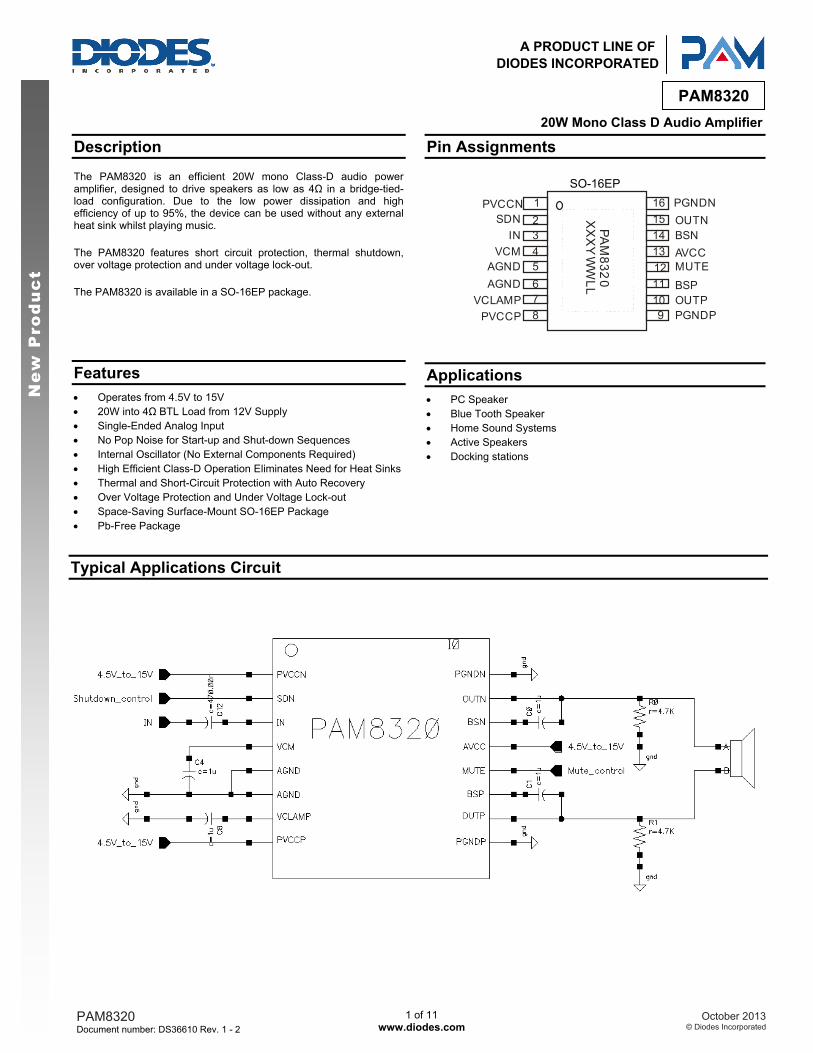
PAM8320 Document number: DS36610 Rev. 1 - 2 1 of 11 www.diodes.com October 2013 © Diodes Incorporated PAM8320 New Product A PRODUCT LINE OF DIODES INCORPORATED 20W Mono Class D Audio Amplifier Description The PAM8320 is an efficient 20W mono Class-D audio power amplifier, designed to drive speakers as low as 4Ω in a bridge-tied- load configuration. Due to the low power dissipation and high efficiency of up to 95%, the device can be used without any external heat sink whilst playing music. The PAM8320 features short circuit protection, thermal shutdown, over voltage protection and under voltage lock-out. The PAM8320 is available in a SO-16EP package. Features Operates from 4.5V to 15V 20W into 4Ω BTL Load from 12V Supply Single-Ended Analog Input No Pop Noise for Start-up and Shut-down Sequences Internal Oscillator (No External Components Required) High Efficient Class-D Operation Eliminates Need for Heat Sinks Thermal and Short-Circuit Protection with Auto Recovery Over Voltage Protection and Under Voltage Lock-out Space-Saving Surface-Mount SO-16EP Package Pb-Free Package Pin Assignments SO-16EP PVCCN SDN MUTE VCM AGND AGND VCLAMP PVCCP PGNDP OUTP BSP AVCC BSN OUTN PGNDN PAM8320 XXXYWWLL 9 1 2 3 4 5 6 7 8 10 11 12 13 14 15 16 IN Applications PC Speaker Blue Tooth Speaker Home Sound Systems Active Speakers Docking stations Typical Applications Circuit
Transcript of 20W Mono Class D Audio Amplifier Description Pin · PDF fileThe PAM8320 is an efficient 20W...
PAM8320 Document number: DS36610 Rev. 1 - 2
1 of 11 www.diodes.com
October 2013© Diodes Incorporated
PAM8320
Ne
w P
rod
uc
t A PRODUCT LINE OF
DIODES INCORPORATED
20W Mono Class D Audio Amplifier
Description
The PAM8320 is an efficient 20W mono Class-D audio power amplifier, designed to drive speakers as low as 4Ω in a bridge-tied-load configuration. Due to the low power dissipation and high efficiency of up to 95%, the device can be used without any external heat sink whilst playing music. The PAM8320 features short circuit protection, thermal shutdown, over voltage protection and under voltage lock-out. The PAM8320 is available in a SO-16EP package.
Features
Operates from 4.5V to 15V 20W into 4Ω BTL Load from 12V Supply Single-Ended Analog Input No Pop Noise for Start-up and Shut-down Sequences Internal Oscillator (No External Components Required) High Efficient Class-D Operation Eliminates Need for Heat Sinks Thermal and Short-Circuit Protection with Auto Recovery Over Voltage Protection and Under Voltage Lock-out Space-Saving Surface-Mount SO-16EP Package Pb-Free Package
Pin Assignments
SO-16EP
PVCCNSDN
MUTEVCM
AGND
AGND
VCLAMP
PVCCP PGNDPOUTPBSP
AVCC
BSNOUTN
PGNDNP
AM
83
20
XX
XY
WW
LL
9
1
23
45
67
810
11
12
13
14
15
16
IN
Applications
PC Speaker Blue Tooth Speaker Home Sound Systems Active Speakers Docking stations
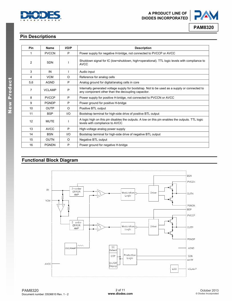
Typical Applications Circuit
PAM8320 Document number: DS36610 Rev. 1 - 2
2 of 11 www.diodes.com
October 2013© Diodes Incorporated
PAM8320
Ne
w P
rod
uc
t A PRODUCT LINE OF
DIODES INCORPORATED
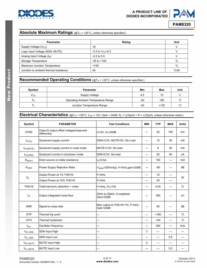
Pin Descriptions
Pin Name I/O/P Description
1 PVCCN P Power supply for negative H-bridge, not connected to PVCCP or AVCC
2 SDN I Shutdown signal for IC (low=shutdown, high=operational). TTL logic levels with compliance to AVCC
3 IN I Audio input
4 VCM O Reference for analog cells
5,6 AGND P Analog ground for digital/analog cells in core
7 VCLAMP P Internally generated voltage supply for bootstrap. Not to be used as a supply or connected to any component other than the decoupling capacitor.
8 PVCCP P Power supply for positive H-bridge, not connected to PVCCN or AVCC
9 PGNDP P Power ground for positive H-bridge
10 OUTP O Positive BTL output
11 BSP I/O Bootstrap terminal for high-side drive of positive BTL output
12 MUTE I A logic high on this pin disables the outputs. A low on this pin enables the outputs. TTL logic levels with compliance to AVCC
13 AVCC P High-voltage analog power supply
14 BSN I/O Bootstrap terminal for high-side drive of negative BTL output
15 OUTN O Negative BTL output
16 PGNDN P Power ground for negative H-bridge
Functional Block Diagram
PAM8320 Document number: DS36610 Rev. 1 - 2
3 of 11 www.diodes.com
October 2013© Diodes Incorporated
PAM8320
Ne
w P
rod
uc
t A PRODUCT LINE OF
DIODES INCORPORATED
Absolute Maximum Ratings (@TA = +25°C, unless otherwise specified.)
Parameter Rating Unit
Supply Voltage (VCC) 18 V
Logic Input Voltage (SDN, MUTE) -0.3 to VCC+0.3 V
Analog Input Voltage (IN) -0.3 to 5.5 V
Storage Temperature -65 to +150 °C
Maximum Junction Temperature +150 °C
Junction to ambient thermal resistance 40 °C/W
Recommended Operating Conditions (@TA = +25°C, unless otherwise specified.)
Symbol Parameter Min Max Unit
VCC Supply Voltage 4.5 15 V
TA Operating Ambient Temperature Range -40 +85 °C
TJ Junction Temperature Range -40 +125 °C
Electrical Characteristics (@TA = +25°C, VCC = 12V, Gain = 20dB, RL = L(33μH) + R + L(33μH), unless otherwise noted.)
Symbol PARAMETER Test Conditions MIN TYP MAX Units
|VOS| Class-D output offset voltage(measured differently) Vi=0V, Av=20dB — 20 100 mV
ICC(q) Quiescent supply current SDN=3.0V, MUTE=0V, No Load — 15 30 mA
ICC(MUTE) Quiescent supply current in mute mode MUTE=2.0V, No load — 8 20 mA
ICC(SDN) Quiescent current in shutdown mode SDN=0.5V, No load — 20 40 uA
Rds(on) Drain-source on-state resistance IO=0.5A — 150 — mΩ
PSRR Power Supply Rejection Ratio Vripple=200mVpp, f=1kHz,gain=20dB — -60 — dB
Po Output Power at 1% THD+N f=1kHz — 15 —
W Output Power at 10% THD+N f=1kHz — 20 —
THD+N Total harmonic distortion + noise f=1kHz, PO=7W — 0.05 — %
Vn Output integrated noise floor 20Hz to 22kHz, A-weighted, Gain=20dB
— 300 — uV
SNR Signal-to-noise ratio Max output at THD+N<1%, f=1kHz, Gain=20dB
— 95 — dB
OTP Thermal trip point — — +160 — °C
OTH Thermal hysteresis — — +40 — °C
fosc Oscillator frequency — — 300 — kHz
VIH_SDN SDN Input High — 3 — — —
VIL_SDN SDN Input Low — — — 0.5 —
VIH_MUTE MUTE Input High — 2 — — —
VIL_MUTE MUTE Input Low — — — 0.5 —
PAM8320 Document number: DS36610 Rev. 1 - 2
4 of 11 www.diodes.com
October 2013© Diodes Incorporated
PAM8320
Ne
w P
rod
uc
t A PRODUCT LINE OF
DIODES INCORPORATED
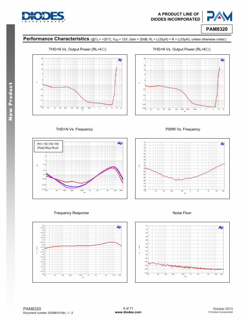
Performance Characteristics (@TA = +25°C, VDD = 12V, Gain = 20dB, RL = L(33μH) + R + L(33μH), unless otherwise noted.)
THD+N Vs. Output Power (RL=4Ω) THD+N Vs. Output Power (RL=8Ω)
THD+N Vs. Frequency PSRR Vs. Frequency
Frequency Response Noise Floor
0.04
50
0.1
0.2
0.5
1
2
5
10
20
%
1m 402m 5m 10m 20m 50m 100m 200m 500m 1 2 5 10 20
W
TTTTTT
0.03
60
0.05
0.1
0.2
0.5
1
2
5
10
20
%
1m 202m 5m 10m 20m 50m 100m 200m 500m 1 2 5 10
W
0.01
20
0.02
0.05
0.1
0.2
0.5
1
2
5
10
%
20 20k50 100 200 500 1k 2k 5k 10k
Hz
-80
+0
-75
-70
-65
-60
-55
-50
-45
-40
-35
-30
-25
-20
-15
-10
-5
dB
20 20k50 100 200 500 1k 2k 5k 10k
Hz
T T T T T
-130
+ 0
-120
-110
-100
-90
-80
-70
-60
-50
-40
-30
-20
-10
dBr
A
20 20k50 100 200 500 1k 2k 5k 10k
Hz
PO=1W/2W/3W (Pink/Blue/Red)
+ 20
+ 30
+ 20.5
+ 21
+ 21.5
+ 22
+ 22.5
+ 23
+ 23.5
+ 24
+ 24.5
+ 25
+ 25.5
+ 26
+ 26.5
+ 27
+ 27.5
+ 28
+ 28.5
+ 29
+ 29.5
dBg
A
20 20k50 100 200 500 1k 2k 5k 10k
Hz
PAM8320 Document number: DS36610 Rev. 1 - 2
5 of 11 www.diodes.com
October 2013© Diodes Incorporated
PAM8320
Ne
w P
rod
uc
t A PRODUCT LINE OF
DIODES INCORPORATED
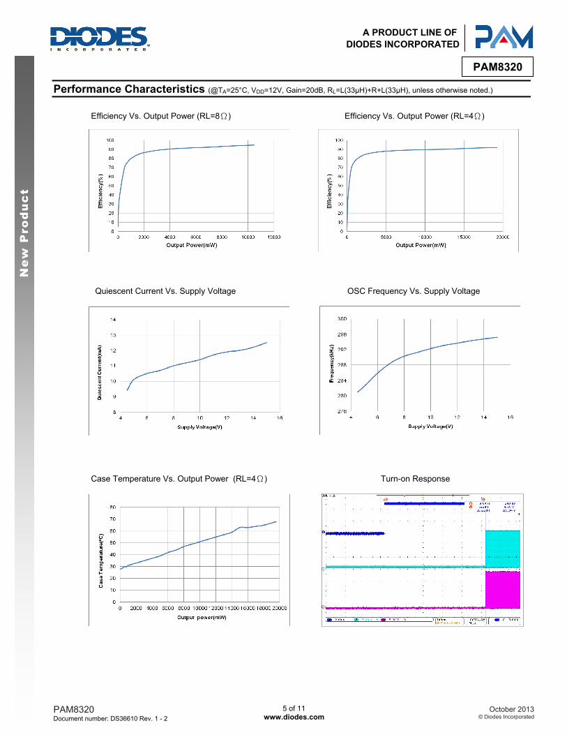
Performance Characteristics (@TA=25°C, VDD=12V, Gain=20dB, RL=L(33μH)+R+L(33μH), unless otherwise noted.)
Efficiency Vs. Output Power (RL=8Ω) Efficiency Vs. Output Power (RL=4Ω)
Quiescent Current Vs. Supply Voltage OSC Frequency Vs. Supply Voltage
Case Temperature Vs. Output Power (RL=4Ω) Turn-on Response
PAM8320 Document number: DS36610 Rev. 1 - 2
6 of 11 www.diodes.com
October 2013© Diodes Incorporated
PAM8320
Ne
w P
rod
uc
t A PRODUCT LINE OF
DIODES INCORPORATED
Application Information
Input Capacitors (Ci)
In the typical application, an input capacitor Ci, is required to allow the amplifier to bias the input signal to the proper DC level for optimum operation. In this case, Ci and the minimum input impedance Ri form is a high-pass filter with the corner frequency determined in the follow equation:
C
1f
2 RiCi
It is important to consider the value of Ci as it directly affects the low frequency performance of the circuit. For example, when Ri is 40kΩ and the specification calls for a flat bass response are down to 20Hz. The equation is reconfigured as followed to determine the value of Ci:
i c
1Ci
2 Rf
When input resistance variation is considered Ci is 200nF, so one would likely choose a value of 220nF. A further consideration for this capacitor is the leakage path from the input source through the input network (Ci, Ri and Rf) to the load. This leakage current creates a DC offset voltage at the input to the amplifier that reduces useful headroom, especially in high gain applications. For this reason, a low-leakage tantalum or ceramic capacitor is the best choice. When polarized capacitors are used, the positive side of the capacitor should face the amplifier input in most applications as the DC level is held at VDD/2, which is likely higher than the source DC level. Please note that it is important to confirm the capacitor polarity in the application.
Input Resistance
The value of the input resistance (Ri) of the amplifier is 40kΩ ±20%. If a single capacitor is added to the input of the high-pass filter the –3dB cutoff frequency can be calculated using equation:
C
1f
2 RiCi
Gain Formula with External Input Resistor
The default gain of PAM8320 is 26dB. The gain can be reduced by adding one external resistor between input decoupling capacitor and IN PIN. The gain formula is as below:
k
RA
xv
400141
20
Note: Rx is external input resistor
Power and Heat Dissipation
Speakers must be chosen to withstand the large output power from the PAM8320, otherwise speaker damage may occur.
Heat dissipation is very important when the device works in full power operation. Two factors affect the heat dissipation, the efficiency of the device that determines the dissipation power and the thermal resistance of the package that determines the heat dissipation capability.
The PAM8320 class-D amplifier is highly efficiency and should not need heat sink. Operating at higher powers a heat sink still may not be necessary if the PCB is carefully designed to achieve good thermal dissipation.
PAM8320 Document number: DS36610 Rev. 1 - 2
7 of 11 www.diodes.com
October 2013© Diodes Incorporated
PAM8320
Ne
w P
rod
uc
t A PRODUCT LINE OF
DIODES INCORPORATED
Dual-Side PCB
To achieve good heat dissipation the PCB's copper plate should be thicker than 35um and the copper plate on both sides of the PCB should be utilized for heat sink.
The thermal pad on the bottom of the device should be soldered to the plate of the PCB and via holes (usually 9 to 16) should be drilled in the PCB area under the device. Deposited copper on the vias should be thick enough so that the heat can be dissipated to the other side of the plate. There should be no insulation mask on the other side of the copper plate. More vias can and should be added to the PCB around the device for further thermal optimization.
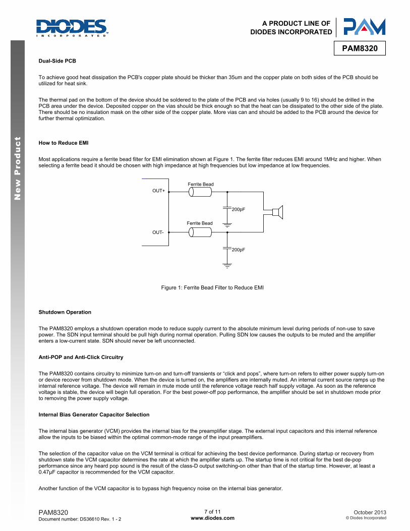
How to Reduce EMI
Most applications require a ferrite bead filter for EMI elimination shown at Figure 1. The ferrite filter reduces EMI around 1MHz and higher. When selecting a ferrite bead it should be chosen with high impedance at high frequencies but low impedance at low frequencies.
200pF
200pF
OUT+
OUT-
Ferrite Bead
Ferrite Bead
Figure 1: Ferrite Bead Filter to Reduce EMI
Shutdown Operation
The PAM8320 employs a shutdown operation mode to reduce supply current to the absolute minimum level during periods of non-use to save power. The SDN input terminal should be pull high during normal operation. Pulling SDN low causes the outputs to be muted and the amplifier enters a low-current state. SDN should never be left unconnected.
Anti-POP and Anti-Click Circuitry
The PAM8320 contains circuitry to minimize turn-on and turn-off transients or “click and pops”, where turn-on refers to either power supply turn-on or device recover from shutdown mode. When the device is turned on, the amplifiers are internally muted. An internal current source ramps up the internal reference voltage. The device will remain in mute mode until the reference voltage reach half supply voltage. As soon as the reference voltage is stable, the device will begin full operation. For the best power-off pop performance, the amplifier should be set in shutdown mode prior to removing the power supply voltage.
Internal Bias Generator Capacitor Selection
The internal bias generator (VCM) provides the internal bias for the preamplifier stage. The external input capacitors and this internal reference allow the inputs to be biased within the optimal common-mode range of the input preamplifiers.
The selection of the capacitor value on the VCM terminal is critical for achieving the best device performance. During startup or recovery from shutdown state the VCM capacitor determines the rate at which the amplifier starts up. The startup time is not critical for the best de-pop performance since any heard pop sound is the result of the class-D output switching-on other than that of the startup time. However, at least a 0.47µF capacitor is recommended for the VCM capacitor.
Another function of the VCM capacitor is to bypass high frequency noise on the internal bias generator.
PAM8320 Document number: DS36610 Rev. 1 - 2
8 of 11 www.diodes.com
October 2013© Diodes Incorporated
PAM8320
Ne
w P
rod
uc
t A PRODUCT LINE OF
DIODES INCORPORATED
Power Supply Decoupling, CS
The PAM8320 is a high-performance CMOS audio amplifier that requires adequate power supply decoupling to ensure the output total harmonic distortion (THD) as low as possible. Power supply decoupling also prevents the oscillations causing by long lead length between the amplifier and the speaker.
Optimum decoupling is achieved by using two different types of capacitors that target different types of noise on the power supply leads. Higher frequency transients, spikes or digital hash should be filtered with a good low equivalent-series-resistance (ESR) ceramic capacitor with a value of typically 0.1μF. This capacitor should be placed as close as possible to the PVCC pin of the device. Lower frequency noise signals should be filtered with a large ceramic capacitor of 470μF or greater. It's recommended to place this capacitor near the audio power amplifier. The 10µF capacitor also serves as a local storage capacitor for supplying current during large signal transients on the amplifier outputs.
BSN and BSP Capacitors
The half H-bridge output stages use NMOS transistors therefore requiring bootstrap capacitors for the high side of each output to turn on correctly. A ceramic capacitor 220nF or more rated for over 25V must be connected from each output to its corresponding bootstrap input. Specifically, one 220nF capacitor must be connected from OUTN to BSN and another 220nF capacitor from OUTP to BSP. It is recommended to use 1μF BST capacitor to replace 220nF for lower than 100Hz applications.
VCLAMP Capacitors
To ensure that the maximum gate-to-source voltage for the NMOS output transistors is not exceeded, an internal regulator is used to clamp the gate voltage. A 1µF capacitor must be connected from VCLAMP to ground and must be rated for at least 25V. The voltages at the VCLAMP terminals vary with VCC and may not be used to power any other circuitry.
Using low-ESR Capacitors
Low-ESR capacitors are recommended throughout this application section. A real (with respect to ideal) capacitor can be modeled simply as a resistor in series with an ideal capacitor. The voltage drop across this resistor minimizes the beneficial effects of the capacitor in the circuit. The lower the equivalent value of this resistance the more the real capacitor behaves as an ideal capacitor.
Short-circuit Protection
The PAM8320 has short circuit protection circuitry on the outputs to prevent damage to the device when output-to-output shorts (BTL mode), output-to-GND shorts, or output-to-VCC shorts occur. Once a short-circuit is detected on the outputs, the output drive is immediately disabled. This is not a latched fault, if the short is removed the normal operation is restored.
Thermal Protection
Thermal protection prevents the device from damage. When the internal die temperature exceeds a typical of 160°C the device will enter a shutdown state and the outputs are disabled. This is not a latched fault, once the thermal fault is cleared and the temperature of the die decreased by 40°C the device will restart with no external system interaction.
Over Voltage Protection and Under Voltage Lock-out (OVP and UVLO)
An over voltage protection (OVP) circuit is integrated in PAM8320, when the supply voltage is over 18V the OVP is active and then the output stage is disabled. The PAM8320 will auto recovery when the supply voltage is lower than the OVP threshold.
The PAM8320 incorporates circuitry designed to detect low supply voltage. When the supply voltage drops to 4.4V or below, the PAM8320 goes into a state of shutdown. When the supply voltage is higher than 4.5V normal operation is resumed.
PAM8320 Document number: DS36610 Rev. 1 - 2
9 of 11 www.diodes.com
October 2013© Diodes Incorporated
PAM8320
Ne
w P
rod
uc
t A PRODUCT LINE OF
DIODES INCORPORATED
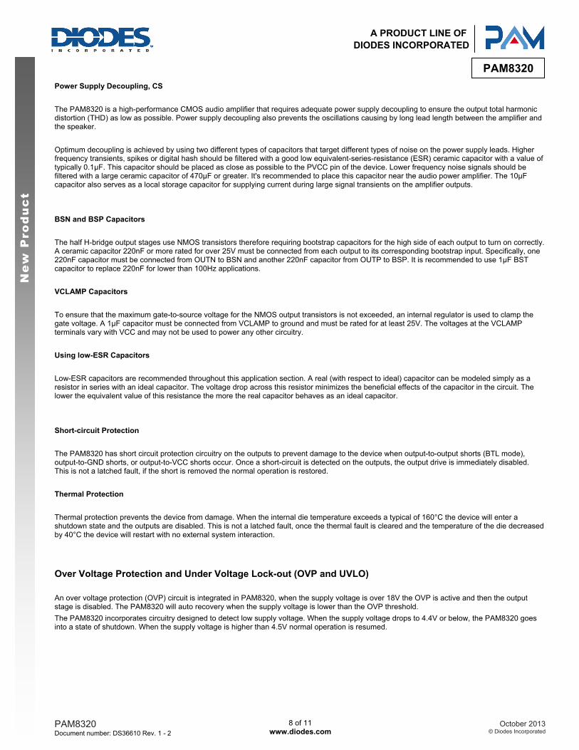
Ordering Information
PAM8320 X X X
R: SOP-16L (EP) D: 16 Pin R: Tape & Real
Part Number Package Standard Package
PAM8320RDR SO-16EP 2,500Units/Tape&Real
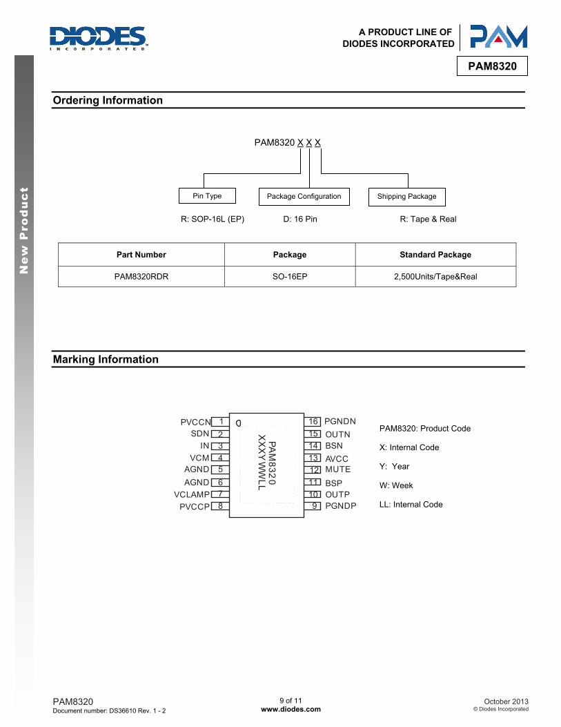
Marking Information
PVCCNSDN
MUTEVCM
AGND
AGND
VCLAMP
PVCCP PGNDPOUTPBSP
AVCC
BSNOUTN
PGNDN
PA
M8
32
0X
XX
YW
WL
L
9
1
23
45
67
810
11
12
13
14
15
16
IN
PAM8320: Product Code X: Internal Code
Y: Year
W: Week
LL: Internal Code
Package Configuration Shipping Package Pin Type
PAM8320 Document number: DS36610 Rev. 1 - 2
10 of 11 www.diodes.com
October 2013© Diodes Incorporated
PAM8320
Ne
w P
rod
uc
t A PRODUCT LINE OF
DIODES INCORPORATED
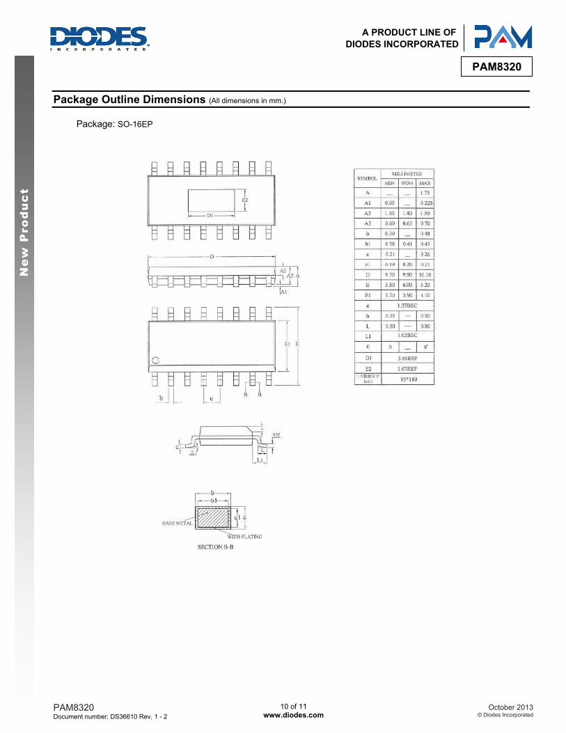
Package Outline Dimensions (All dimensions in mm.)
Package: SO-16EP
PAM8320 Document number: DS36610 Rev. 1 - 2
11 of 11 www.diodes.com
October 2013© Diodes Incorporated
PAM8320
Ne
w P
rod
uc
t A PRODUCT LINE OF
DIODES INCORPORATED
IMPORTANT NOTICE DIODES INCORPORATED MAKES NO WARRANTY OF ANY KIND, EXPRESS OR IMPLIED, WITH REGARDS TO THIS DOCUMENT, INCLUDING, BUT NOT LIMITED TO, THE IMPLIED WARRANTIES OF MERCHANTABILITY AND FITNESS FOR A PARTICULAR PURPOSE (AND THEIR EQUIVALENTS UNDER THE LAWS OF ANY JURISDICTION). Diodes Incorporated and its subsidiaries reserve the right to make modifications, enhancements, improvements, corrections or other changes without further notice to this document and any product described herein. Diodes Incorporated does not assume any liability arising out of the application or use of this document or any product described herein; neither does Diodes Incorporated convey any license under its patent or trademark rights, nor the rights of others. Any Customer or user of this document or products described herein in such applications shall assume all risks of such use and will agree to hold Diodes Incorporated and all the companies whose products are represented on Diodes Incorporated website, harmless against all damages. Diodes Incorporated does not warrant or accept any liability whatsoever in respect of any products purchased through unauthorized sales channel. Should Customers purchase or use Diodes Incorporated products for any unintended or unauthorized application, Customers shall indemnify and hold Diodes Incorporated and its representatives harmless against all claims, damages, expenses, and attorney fees arising out of, directly or indirectly, any claim of personal injury or death associated with such unintended or unauthorized application. Products described herein may be covered by one or more United States, international or foreign patents pending. Product names and markings noted herein may also be covered by one or more United States, international or foreign trademarks. This document is written in English but may be translated into multiple languages for reference. Only the English version of this document is the final and determinative format released by Diodes Incorporated.
LIFE SUPPORT Diodes Incorporated products are specifically not authorized for use as critical components in life support devices or systems without the express written approval of the Chief Executive Officer of Diodes Incorporated. As used herein: A. Life support devices or systems are devices or systems which: 1. are intended to implant into the body, or
2. support or sustain life and whose failure to perform when properly used in accordance with instructions for use provided in the labeling can be reasonably expected to result in significant injury to the user.
B. A critical component is any component in a life support device or system whose failure to perform can be reasonably expected to cause the failure of the life support device or to affect its safety or effectiveness. Customers represent that they have all necessary expertise in the safety and regulatory ramifications of their life support devices or systems, and acknowledge and agree that they are solely responsible for all legal, regulatory and safety-related requirements concerning their products and any use of Diodes Incorporated products in such safety-critical, life support devices or systems, notwithstanding any devices- or systems-related information or support that may be provided by Diodes Incorporated. Further, Customers must fully indemnify Diodes Incorporated and its representatives against any damages arising out of the use of Diodes Incorporated products in such safety-critical, life support devices or systems. Copyright © 2013, Diodes Incorporated www.diodes.com