MAX9709 25W/50W, Filterless, Spread-Spectrum, Stereo/Mono ...
20
General Description The MAX9709 stereo/mono, Class D audio power ampli- fier delivers up to 2 x 25W into an 8Ω stereo mode and 1 x 50W into a 4Ω load in mono mode while offering up to 87% efficiency. The MAX9709 provides Class AB ampli- fier performance with the benefits of Class D efficiency, eliminating the need for a bulky heatsink and conserving power. The MAX9709 operates from a single +10V to +22V supply, driving the load in a BTL configuration. The MAX9709 offers two modulation schemes: a fixed- frequency modulation (FFM) mode, and a spread-spec- trum modulation (SSM) mode that reduces EMI-radiated emissions. The MAX9709 can be synchronized to an external clock from 600kHz to 1.2MHz. A synchronized output allows multiple units to be cascaded in the system. Features include fully differential inputs, comprehen- sive click-and-pop suppression, and four selectable-gain settings (22dB, 25dB, 29.5dB, and 36dB). A pin-pro- grammable thermal flag provides seven different ther- mal warning thresholds. Short-circuit and thermal-over- load protection prevent the device from being damaged during a fault condition. The MAX9709 is available in a 56-pin TQFN (8mm x 8mm x 0.8mm) package, and is specified over the extended -40°C to +85°C temperature range. Applications Features ● 2 x 25W Output Power in Stereo Mode (8Ω, THD = 10%) ● 1 x 50W Output Power in Mono Mode (4Ω, THD = 10%) ● High Efficiency: Up to 87% ● Filterless Class D Amplifier ● Unique Spread-Spectrum Mode ● Programmable Gain (+22dB, +25dB, +29.5dB, +36dB) ● High PSRR (90dB at 1kHz) ● Differential Inputs Suppress Common-Mode Noise ● Shutdown and Mute Control ● Integrated Click-and-Pop Suppression ● Low 0.1% THD+N ● Current Limit and Thermal Protection ● Programmable Thermal Flag ● Clock Synchronization Input and Output ● Available in Thermally Efficient, Space-Saving Package: 56-Pin TQFN Pin Configurations appear at end of data sheet. 19-3769; Rev 2; 5/14 ● LCD TVs ● PDP TVs ● PC/HiFi Audio Solutions +Denotes a lead-free package. **EP = Exposed pad. PART TEMP RANGE PIN-PACKAGE MAX9709ETN+ -40°C to +85°C 56 TQFN-EP** CLASS D MODULATOR SYNCOUT TEMP OUTPUT PROTECTION GAIN CONTROL FS1, FS2 MAX9709 STEREO MODE G1, G2 2 SYNC RIGHT CHANNEL LEFT CHANNEL MONO 2 TH0, TH1, TH2 3 CLASS D MODULATOR SYNCOUT TEMP OUTPUT PROTECTION GAIN CONTROL FS1, FS2 MAX9709 MONO MODE G1, G2 2 SYNC AUDIO INPUT VDIGITAL MONO 2 TH0, TH1, TH2 3 MAX9709 25W/50W, Filterless, Spread-Spectrum, Stereo/Mono, Class D Amplifier Simplified Block Diagram Ordering Information EVALUATION KIT AVAILABLE
-
Upload
duongkhanh -
Category
Documents
-
view
220 -
download
1
Transcript of MAX9709 25W/50W, Filterless, Spread-Spectrum, Stereo/Mono ...
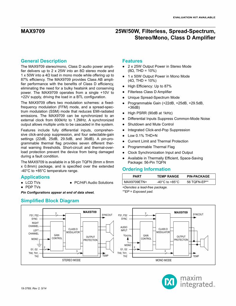
General DescriptionThe MAX9709 stereo/mono, Class D audio power ampli-fier delivers up to 2 x 25W into an 8Ω stereo mode and 1 x 50W into a 4Ω load in mono mode while offering up to 87% efficiency. The MAX9709 provides Class AB ampli-fier performance with the benefits of Class D efficiency, eliminating the need for a bulky heatsink and conserving power. The MAX9709 operates from a single +10V to +22V supply, driving the load in a BTL configuration.The MAX9709 offers two modulation schemes: a fixed-frequency modulation (FFM) mode, and a spread-spec-trum modulation (SSM) mode that reduces EMI-radiated emissions. The MAX9709 can be synchronized to an external clock from 600kHz to 1.2MHz. A synchronized output allows multiple units to be cascaded in the system.Features include fully differential inputs, comprehen-sive click-and-pop suppression, and four selectable-gain settings (22dB, 25dB, 29.5dB, and 36dB). A pin-pro-grammable thermal flag provides seven different ther-mal warning thresholds. Short-circuit and thermal-over-load protection prevent the device from being damaged during a fault condition.The MAX9709 is available in a 56-pin TQFN (8mm x 8mm x 0.8mm) package, and is specified over the extended -40°C to +85°C temperature range.
Applications
Features 2 x 25W Output Power in Stereo Mode
(8Ω, THD = 10%) 1 x 50W Output Power in Mono Mode
(4Ω, THD = 10%) High Efficiency: Up to 87% Filterless Class D Amplifier Unique Spread-Spectrum Mode Programmable Gain (+22dB, +25dB, +29.5dB,
+36dB) High PSRR (90dB at 1kHz) Differential Inputs Suppress Common-Mode Noise Shutdown and Mute Control Integrated Click-and-Pop Suppression Low 0.1% THD+N Current Limit and Thermal Protection Programmable Thermal Flag Clock Synchronization Input and Output Available in Thermally Efficient, Space-Saving
Package: 56-Pin TQFN
Pin Configurations appear at end of data sheet.
19-3769; Rev 2; 5/14
LCD TVs PDP TVs
PC/HiFi Audio Solutions+Denotes a lead-free package.**EP = Exposed pad.
PART TEMP RANGE PIN-PACKAGEMAX9709ETN+ -40°C to +85°C 56 TQFN-EP**
CLASS DMODULATOR
SYNCOUT
TEMP
OUTPUTPROTECTION
GAIN CONTROL
FS1, FS2MAX9709
STEREO MODE
G1, G22
SYNCRIGHT
CHANNELLEFT
CHANNEL
MONO
2
TH0, TH1,TH2
3
CLASS DMODULATOR
SYNCOUT
TEMP
OUTPUTPROTECTION
GAIN CONTROL
FS1, FS2MAX9709
MONO MODE
G1, G22
SYNC
AUDIOINPUT
VDIGITAL
MONO
2
TH0, TH1, TH2
3
MAX9709 25W/50W, Filterless, Spread-Spectrum, Stereo/Mono, Class D Amplifier
Simplified Block Diagram
Ordering Information
EVALUATION KIT AVAILABLE
PVDD, VDD to PGND, GND .................................... -0.3 to +30VPVDD to VDD ........................................................-0.3V to +0.3VOUTR+, OUTR-, OUTL+,
OUTL- to PGND, GND .......................-0.3V to (PVDD + 0.3V)C1N to GND ...........................................-0.3V to (PVDD + 0.3V)C1P to GND .......................... (PVDD - 0.3V) to (CPVDD + 0.3V)CPVDD to GND .......................................(PVDD - 0.3V) to +40VAll Other Pins to GND ...........................................-0.3V to +12VContinuous Input Current (except PVDD, VDD, OUTR+,
OUTR-, OUTL+, and OUTL-) .........................................20mA
Continuous Power Dissipation (TA = +70°C) 56-Pin Thin QFN (derate 47.6mW/°C above +70°C) ....3.81W
Operating Temperature Range ........................... -40°C to +85°CStorage Temperature Range ............................ -65°C to +150°CJunction Temperature ......................................................+150°CThermal Resistance (θJC)
56-Pin Thin QFN .........................................................0.6°C/WLead Temperature (soldering, 10s) .................................+300°C
(PVDD = VDD = +20V, PGND = GND = 0V, CSS = 0.47µF, CREG = 0.01µF, C1 = 0.1µF, C2 = 1µF, RLOAD = ∞, MONO = low (stereo mode), SHDN = MUTE = high, G1 = low, G2 = high (AV = 22dB), FS1 = FS2 = high (SSM), SYNCIN = low. All load resistors (RL) are connected between OUT_+ and OUT_-, unless otherwise stated. TA = TMIN to TMAX, unless otherwise noted. Typical values are at TA = +25°C.) (Note 1)
PARAMETER SYMBOL CONDITIONS MIN TYP MAX UNITSSupply Voltage Range VDD Inferred from PSRR test 10 22 V
Shutdown Current ISHDN SHDN = low 0.1 1 µA
Shutdown to Full Operation tSON 100 ms
Mute to Full Operation tMUTE 100 ms
Input Impedance RIN
G1 = 0, G2 = 1 50 85 125
kΩG1 = 1, G2 = 1 40 63 90
G1 = 1, G2 = 0 25 43 60
G1 = 0, G2 = 0 12 21 30
Output Pulldown Resistance SHDN = GND 600 kΩ
Output Offset Voltage VOSAC-coupled input, measured between OUT_+ and OUT_- 3 ±40 mV
Power-Supply Rejection Ratio PSRR
PVDD = 10V to 22V 67 90
dB200mVP-P ripple (Note 2)
fRIPPLE = 1kHz 90
fRIPPLE = 20kHz 52
Common-Mode Rejection Ratio CMRRDC, input referred 49 70
dBf = 20Hz to 20kHz, input referred 60
Switch On-Resistance RDS One power switch 0.3 0.6 Ω
Switching Frequency fSW
FS1 FS2
kHz
0 0 180 200 220
1 1 (SSM) 200
1 0 160
0 1 250
Oscillator Spread Bandwidth FS1 = FS2 = high (SSM) ±2 %
SYNCIN Lock Range Equal to fSW x 4 600 1200 kHz
MAX9709 25W/50W, Filterless, Spread-Spectrum, Stereo/Mono, Class D Amplifier
www.maximintegrated.com Maxim Integrated 2
Absolute Maximum Ratings
Stresses beyond those listed under “Absolute Maximum Ratings” may cause permanent damage to the device. These are stress ratings only, and functional operation of the device at these or any other conditions beyond those indicated in the operational sections of the specifications is not implied. Exposure to absolute maximum rating conditions for extended periods may affect device reliability.
Electrical Characteristics
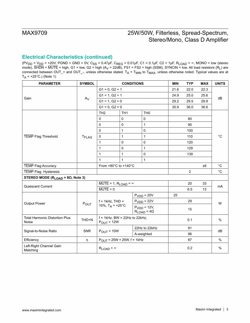
(PVDD = VDD = +20V, PGND = GND = 0V, CSS = 0.47µF, CREG = 0.01µF, C1 = 0.1µF, C2 = 1µF, RLOAD = ∞, MONO = low (stereo mode), SHDN = MUTE = high, G1 = low, G2 = high (AV = 22dB), FS1 = FS2 = high (SSM), SYNCIN = low. All load resistors (RL) are connected between OUT_+ and OUT_-, unless otherwise stated. TA = TMIN to TMAX, unless otherwise noted. Typical values are at TA = +25°C.) (Note 1)
PARAMETER SYMBOL CONDITIONS MIN TYP MAX UNITS
Gain AV
G1 = 0, G2 = 1 21.6 22.0 22.3
dBG1 = 1, G2 = 1 24.9 25.0 25.6
G1 = 1, G2 = 0 29.2 29.5 29.9
G1 = 0, G2 = 0 35.9 36.0 36.6
TEMP Flag Threshold TFLAG
TH2 TH1 TH0
°C
0 0 0 80
0 0 1 90
0 1 0 100
0 1 1 110
1 0 0 120
1 0 1 129
1 1 0 139
1 1 1
TEMP Flag Accuracy From +80°C to +140°C ±6 °C
TEMP Flag Hysteresis 2 °C
STEREO MODE (RLOAD = 8Ω, Note 3)
Quiescent Current MUTE = 1, RLOAD = ∞ 20 33
mAMUTE = 0 6.5 13
Output Power POUTf = 1kHz, THD = 10%, TA = +25°C
PVDD = 20V 25
WPVDD = 22V 29
PVDD = 12V, RLOAD = 4Ω 15
Total Harmonic Distortion Plus Noise THD+N f = 1kHz, BW = 22Hz to 22kHz,
POUT = 12W 0.1 %
Signal-to-Noise Ratio SNR POUT = 10W22Hz to 22kHz 91
dBA-weighted 96
Efficiency η POUT = 25W + 25W, f = 1kHz 87 %
Left-Right Channel Gain Matching RLOAD = ∞ 0.2 %
MAX9709 25W/50W, Filterless, Spread-Spectrum, Stereo/Mono, Class D Amplifier
www.maximintegrated.com Maxim Integrated 3
Electrical Characteristics (continued)

(PVDD = VDD = +20V, PGND = GND = 0V, CSS = 0.47µF, CREG = 0.01µF, C1 = 0.1µF, C2 = 1µF, RLOAD = ∞, MONO = low (stereo mode), SHDN = MUTE = high, G1 = low, G2 = high (AV = 22dB), FS1 = FS2 = high (SSM), SYNCIN = low. All load resistors (RL) are connected between OUT_+ and OUT_-, unless otherwise stated. TA = TMIN to TMAX, unless otherwise noted. Typical values are at TA = +25°C.) (Note 1)
Note 1: All devices are 100% production tested at +25°C. All temperature limits are guaranteed by design.Note 2: Inputs AC-coupled to GND.Note 3: Testing performed with an 8Ω resistive load in series with a 68µH inductive load across the BTL outputs.Note 4: Minimum output power is guaranteed by pulse testing.Note 5: Testing performed with an 8Ω resistive load in series with a 68µH inductive load connected across BTL outputs. Mode tran-
sitions are controlled by SHDN.Note 6: Testing performed with a 4Ω resistive load in series with a 33µH inductive load across the BTL outputs.
PARAMETER SYMBOL CONDITIONS MIN TYP MAX UNITS
Output Short-Circuit Current Threshold ISC RLOAD = 0Ω 3 A
Click-and-Pop Level KCPPeak voltage, 32 samples/second, A-weighted (Notes 2, 5)
Into shutdown -63dBV
Out of shutdown -55
MONO MODE (RLOAD = 4Ω, MONO = HIGH) (Note 6)
Quiescent Current MUTE = 1, RLOAD = ∞ 20
mAMUTE = 0 6.5
Output Power POUT f = 1kHz, THD = 10%RLOAD = 8Ω 25
WRLOAD = 4Ω 50
Total Harmonic Distortion Plus Noise THD+N f = 1kHz, BW = 22Hz to 22kHz,
POUT = 22W 0.09 %
Signal-to-Noise Ratio SNR POUT = 10W20Hz to 20kHz 91
dBA-weighted 95
Efficiency η POUT = 54W, f = 1kHz 86 %
Output Short-Circuit Current Threshold ISC RLOAD = 0Ω 6 A
Click-and-Pop Level KCPPeak voltage, 32 samples/second, A-weighted (Notes 2, 5)
Into shutdown -60dBV
Out of shutdown -63
DIGITAL INPUTS (SHDN, MUTE, G1, G2, FS1, FS2, TH0, TH1, TH2, SYNCIN, MONO)Logic-Input Current IIN 0 to 12V 1 µA
Logic-Input High Voltage VIH 2.5 V
Logic-Input Low Voltage VIL 0.8 V
OPEN-DRAIN OUTPUTS (TEMP, SYNCOUT)Open-Drain Output Low Voltage VOL ISINK = 3mA 0.4 V
Leakage Current ILEAK VPULLUP = 5.5V 0.2 µA
MAX9709 25W/50W, Filterless, Spread-Spectrum, Stereo/Mono, Class D Amplifier
www.maximintegrated.com Maxim Integrated 4
Electrical Characteristics (continued)
(PVDD = VDD = +20V, PGND = GND = 0V, CSS = 0.47µF, CREG = 0.01µF, C1 = 0.1µF, C2 = 1µF, RLOAD = 8Ω, SHDN = high, MONO = low, MUTE = high, G1 = low, G2 = high, FS1 = FS2 = high (SSM), SYNCIN = low. All load resistors (RL) are between OUT_+ and OUT_-, TA = +25°C, unless otherwise stated.)
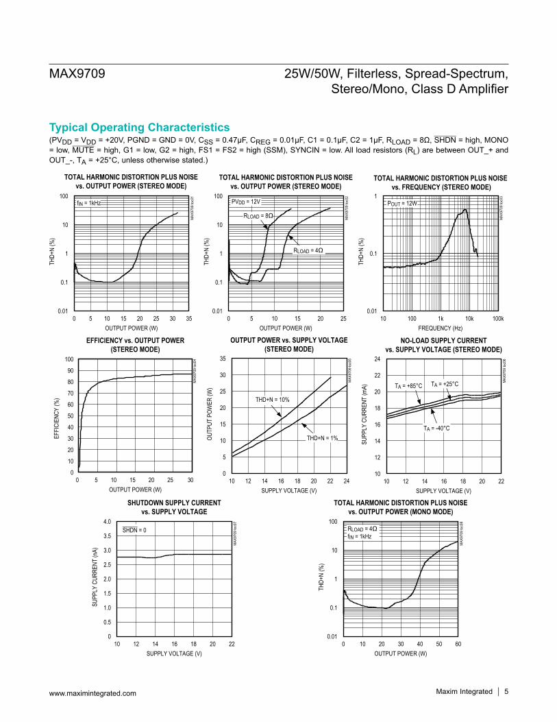
TOTAL HARMONIC DISTORTION PLUS NOISEvs. OUTPUT POWER (STEREO MODE)
MAX
9709
toc0
2
OUTPUT POWER (W)
THD+
N (%
)
2015105
0.1
1
10
100
0.010 25
RLOAD = 4Ω
RLOAD = 8Ω
PVDD = 12V
TOTAL HARMONIC DISTORTION PLUS NOISE vs. FREQUENCY (STEREO MODE)
MAX
9709
toc0
3
FREQUENCY (Hz)
THD+
N (%
)
10k1k100
0.1
10 100k
1
0.01
POUT = 12W
EFFICIENCY vs. OUTPUT POWER(STEREO MODE)
MAX
9709
toc0
4
OUTPUT POWER (W)
EFFI
CIEN
CY (%
)
252015105
10
20
30
40
50
60
70
80
90
100
0030
OUTPUT POWER vs. SUPPLY VOLTAGE(STEREO MODE)
MAX
9709
toc0
5
SUPPLY VOLTAGE (V)
OUTP
UT P
OWER
(W)
222018161412
5
10
15
20
25
30
35
010 24
THD+N = 1%
THD+N = 10%
NO-LOAD SUPPLY CURRENTvs. SUPPLY VOLTAGE (STEREO MODE)
MAX
9709
toc0
6
SUPPLY VOLTAGE (V)
SUPP
LY C
URRE
NT (m
A)
2018161412
12
14
16
18
20
22
24
1010 22
TA = +25°CTA = +85°C
TA = -40°C
SHUTDOWN SUPPLY CURRENTvs. SUPPLY VOLTAGE
MAX
9709
toc0
7
SUPPLY VOLTAGE (V)
SUPP
LY C
URRE
NT (n
A)
201812 14 16
0.5
1.0
1.5
2.0
2.5
3.0
3.5
4.0
010 22
SHDN = 0
TOTAL HARMONIC DISTORTION PLUS NOISEvs. OUTPUT POWER (STEREO MODE)
MAX
9709
toc0
1
OUTPUT POWER (W)
THD+
N (%
)
30252015105
0.1
1
10
100
0.010 35
fIN = 1kHz
TOTAL HARMONIC DISTORTION PLUS NOISEvs. OUTPUT POWER (MONO MODE)
MAX
9709
toc0
8
OUTPUT POWER (W)
THD+
N (%
)
5040302010
0.1
1
10
100
0.010 60
RLOAD = 4ΩfIN = 1kHz
MAX9709 25W/50W, Filterless, Spread-Spectrum, Stereo/Mono, Class D Amplifier
Maxim Integrated 5www.maximintegrated.com
Typical Operating Characteristics
(PVDD = VDD = +20V, PGND = GND = 0V, CSS = 0.47µF, CREG = 0.01µF, C1 = 0.1µF, C2 = 1µF, RLOAD = 8Ω, SHDN = high, MONO = low, MUTE = high, G1 = low, G2 = high, FS1 = FS2 = high (SSM), SYNCIN = low. All load resistors (RL) are between OUT_+ and OUT_-, TA = +25°C, unless otherwise stated.)
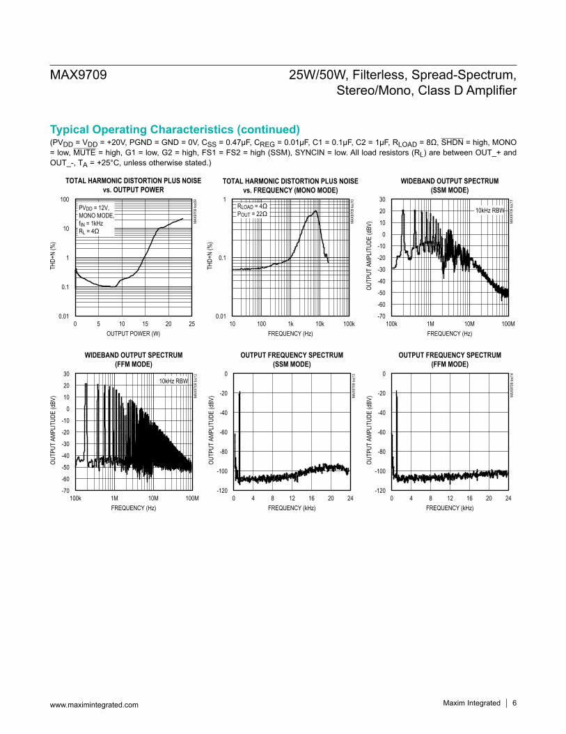
TOTAL HARMONIC DISTORTION PLUS NOISEvs. OUTPUT POWER
MAX
9709
toc0
9
OUTPUT POWER (W)
THD+
N (%
)
2015105
0.1
1
10
100
0.010 25
PVDD = 12V, MONO MODE,fIN = 1kHzRL = 4Ω
TOTAL HARMONIC DISTORTION PLUS NOISEvs. FREQUENCY (MONO MODE)
MAX
9709
toc1
0
FREQUENCY (Hz)
THD+
N (%
)
10k1k100
0.1
10 100k
1
0.01
RLOAD = 4ΩPOUT = 22Ω
WIDEBAND OUTPUT SPECTRUM(SSM MODE)
MAX
9709
toc1
1
FREQUENCY (Hz)
OUTP
UT A
MPLIT
UDE
(dBV
)
10M1M
-60
-50
-40
-30
-20
-10
0
10
20
30
-70100k 100M
10kHz RBW
WIDEBAND OUTPUT SPECTRUM(FFM MODE)
MAX
9709
toc1
2
FREQUENCY (Hz)
OUTP
UT A
MPLIT
UDE
(dBV
)
10M1M100k 100M
10kHz RBW
-60
-50
-40
-30
-20
-10
0
10
20
30
-70
OUTPUT FREQUENCY SPECTRUM(SSM MODE)
MAX
9709
toc1
3
FREQUENCY (kHz)
OUTP
UT A
MPLIT
UDE
(dBV
)
20161284
-100
-80
-60
-40
-20
0
-1200 24
OUTPUT FREQUENCY SPECTRUM(FFM MODE)
MAX
9709
toc1
4FREQUENCY (kHz)
OUTP
UT A
MPLIT
UDE
(dBV
)
20161284
-100
-80
-60
-40
-20
0
-1200 24
MAX9709 25W/50W, Filterless, Spread-Spectrum, Stereo/Mono, Class D Amplifier
Maxim Integrated 6www.maximintegrated.com
Typical Operating Characteristics (continued)
(PVDD = VDD = +20V, PGND = GND = 0V, CSS = 0.47µF, CREG = 0.01µF, C1 = 0.1µF, C2 = 1µF, RLOAD = 8Ω, SHDN = high, MONO = low, MUTE = high, G1 = low, G2 = high, FS1 = FS2 = high (SSM), SYNCIN = low. All load resistors (RL) are between OUT_+ and OUT_-, TA = +25°C, unless otherwise stated.)
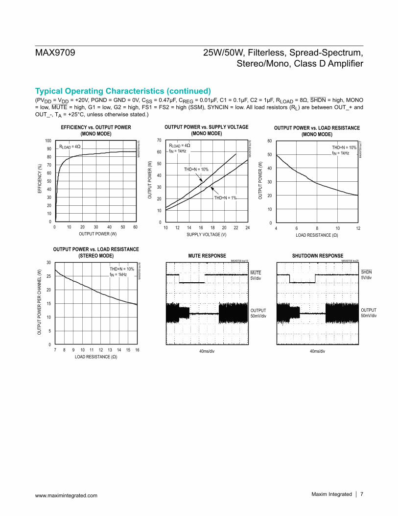
EFFICIENCY vs. OUTPUT POWER(MONO MODE)
MAX
9709
toc1
5
OUTPUT POWER (W)
EFFI
CIEN
CY (%
)
5040302010
10
20
30
40
50
60
70
80
90
100
0060
RLOAD = 4Ω
OUTPUT POWER vs. SUPPLY VOLTAGE(MONO MODE)
MAX
9709
toc1
6
SUPPLY VOLTAGE (V)
OUTP
UT P
OWER
(W)
222018161412
10
20
30
40
50
60
70
010 24
THD+N = 1%
THD+N = 10%
RLOAD = 4ΩfIN = 1kHz
OUTPUT POWER vs. LOAD RESISTANCE(MONO MODE)
MAX
9709
toc1
7
LOAD RESISTANCE (Ω)
OUTP
UT P
OWER
(W)
1086
10
20
30
40
50
60
04 12
THD+N = 10%fIN = 1kHz
OUTPUT POWER vs. LOAD RESISTANCE(STEREO MODE)
MAX
9709
toc1
8
LOAD RESISTANCE (Ω)
OUTP
UT P
OWER
PER
CHA
NNEL
(W)
15141312111098
5
10
15
20
25
30
07 16
THD+N = 10%fIN = 1kHz
MUTE RESPONSEMAX9709 toc19
40ms/div
MUTE5V/div
OUTPUT50mV/div
SHUTDOWN RESPONSEMAX9709 toc20
40ms/div
SHDN5V/div
OUTPUT50mV/div
MAX9709 25W/50W, Filterless, Spread-Spectrum, Stereo/Mono, Class D Amplifier
Maxim Integrated 7www.maximintegrated.com
Typical Operating Characteristics (continued)
(PVDD = VDD = +20V, PGND = GND = 0V, CSS = 0.47µF, CREG = 0.01µF, C1 = 0.1µF, C2 = 1µF, RLOAD = 8Ω, SHDN = high, MONO = low, MUTE = high, G1 = low, G2 = high, FS1 = FS2 = high (SSM), SYNCIN = low. All load resistors (RL) are between OUT_+ and OUT_-, TA = +25°C, unless otherwise stated.)
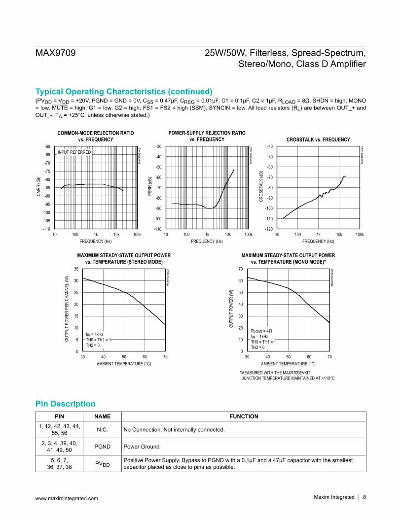
PIN NAME FUNCTION
1, 12, 42, 43, 44, 55, 56 N.C. No Connection. Not internally connected.
2, 3, 4, 39, 40, 41, 49, 50 PGND Power Ground
5, 6, 7, 36, 37, 38 PVDD
Positive Power Supply. Bypass to PGND with a 0.1µF and a 47µF capacitor with the smallest capacitor placed as close to pins as possible.
COMMON-MODE REJECTION RATIOvs. FREQUENCY
MAX
9709
toc2
1
FREQUENCY (Hz)
CMRR
(dB)
10k1k100
-105
-100
-95
-90
-85
-80
-75
-70
-65
-60
-11010 100k
INPUT REFERRED
POWER-SUPPLY REJECTION RATIOvs. FREQUENCY
MAX
9709
toc2
2
FREQUENCY (Hz)
PSRR
(dB)
10k1k100
-100
-90
-80
-70
-60
-50
-40
-30
-11010 100k
CROSSTALK vs. FREQUENCY
MAX
9709
toc2
3
FREQUENCY (Hz)
CROS
STAL
K (d
B)
10k1k100
-110
-100
-90
-80
-70
-60
-50
-40
-12010 100k
MAXIMUM STEADY-STATE OUTPUT POWERvs. TEMPERATURE (STEREO MODE)
MAX
9709
toc2
4
AMBIENT TEMPERATURE (°C)
OUTP
UT P
OWER
PER
CHA
NNEL
(W)
605040
5
10
15
20
25
30
35
030 70
fIN = 1kHzTH0 = TH1 = 1TH2 = 0
MAXIMUM STEADY-STATE OUTPUT POWERvs. TEMPERATURE (MONO MODE)*
MAX
9709
toc2
5
AMBIENT TEMPERATURE (°C)
OUTP
UT P
OWER
(W)
605040
10
20
30
40
50
60
70
030
*MEASURED WITH THE MAX9709EVKIT, JUNCTION TEMPERATURE MAINTAINED AT +110°C.
70
RLOAD = 4ΩfIN = 1kHzTH0 = TH1 = 1TH2 = 0
MAX9709 25W/50W, Filterless, Spread-Spectrum, Stereo/Mono, Class D Amplifier
Maxim Integrated 8www.maximintegrated.com
Typical Operating Characteristics (continued)
Pin Description
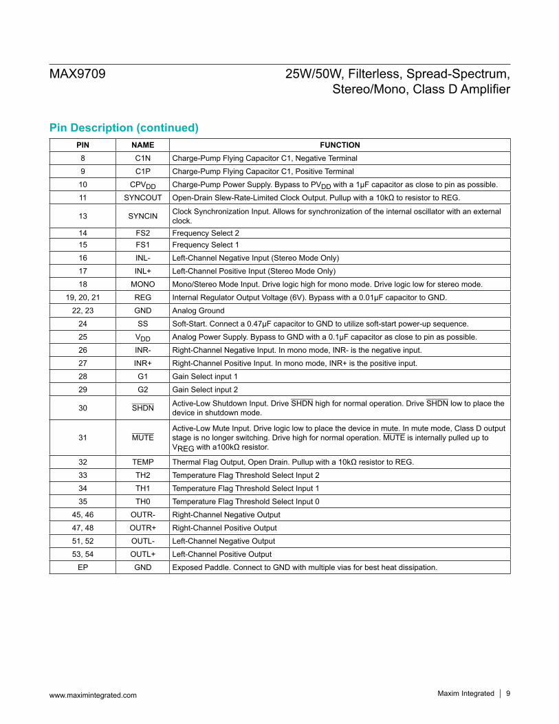
PIN NAME FUNCTION8 C1N Charge-Pump Flying Capacitor C1, Negative Terminal
9 C1P Charge-Pump Flying Capacitor C1, Positive Terminal
10 CPVDD Charge-Pump Power Supply. Bypass to PVDD with a 1µF capacitor as close to pin as possible.
11 SYNCOUT Open-Drain Slew-Rate-Limited Clock Output. Pullup with a 10kΩ to resistor to REG.
13 SYNCIN Clock Synchronization Input. Allows for synchronization of the internal oscillator with an external clock.
14 FS2 Frequency Select 215 FS1 Frequency Select 1
16 INL- Left-Channel Negative Input (Stereo Mode Only)
17 INL+ Left-Channel Positive Input (Stereo Mode Only)
18 MONO Mono/Stereo Mode Input. Drive logic high for mono mode. Drive logic low for stereo mode.
19, 20, 21 REG Internal Regulator Output Voltage (6V). Bypass with a 0.01µF capacitor to GND.
22, 23 GND Analog Ground
24 SS Soft-Start. Connect a 0.47µF capacitor to GND to utilize soft-start power-up sequence.
25 VDD Analog Power Supply. Bypass to GND with a 0.1µF capacitor as close to pin as possible.
26 INR- Right-Channel Negative Input. In mono mode, INR- is the negative input.
27 INR+ Right-Channel Positive Input. In mono mode, INR+ is the positive input.
28 G1 Gain Select input 1
29 G2 Gain Select input 2
30 SHDN Active-Low Shutdown Input. Drive SHDN high for normal operation. Drive SHDN low to place the device in shutdown mode.
31 MUTEActive-Low Mute Input. Drive logic low to place the device in mute. In mute mode, Class D output stage is no longer switching. Drive high for normal operation. MUTE is internally pulled up to VREG with a100kΩ resistor.
32 TEMP Thermal Flag Output, Open Drain. Pullup with a 10kΩ resistor to REG.
33 TH2 Temperature Flag Threshold Select Input 2
34 TH1 Temperature Flag Threshold Select Input 1
35 TH0 Temperature Flag Threshold Select Input 0
45, 46 OUTR- Right-Channel Negative Output
47, 48 OUTR+ Right-Channel Positive Output
51, 52 OUTL- Left-Channel Negative Output
53, 54 OUTL+ Left-Channel Positive Output
EP GND Exposed Paddle. Connect to GND with multiple vias for best heat dissipation.
MAX9709 25W/50W, Filterless, Spread-Spectrum, Stereo/Mono, Class D Amplifier
www.maximintegrated.com Maxim Integrated 9
Pin Description (continued)
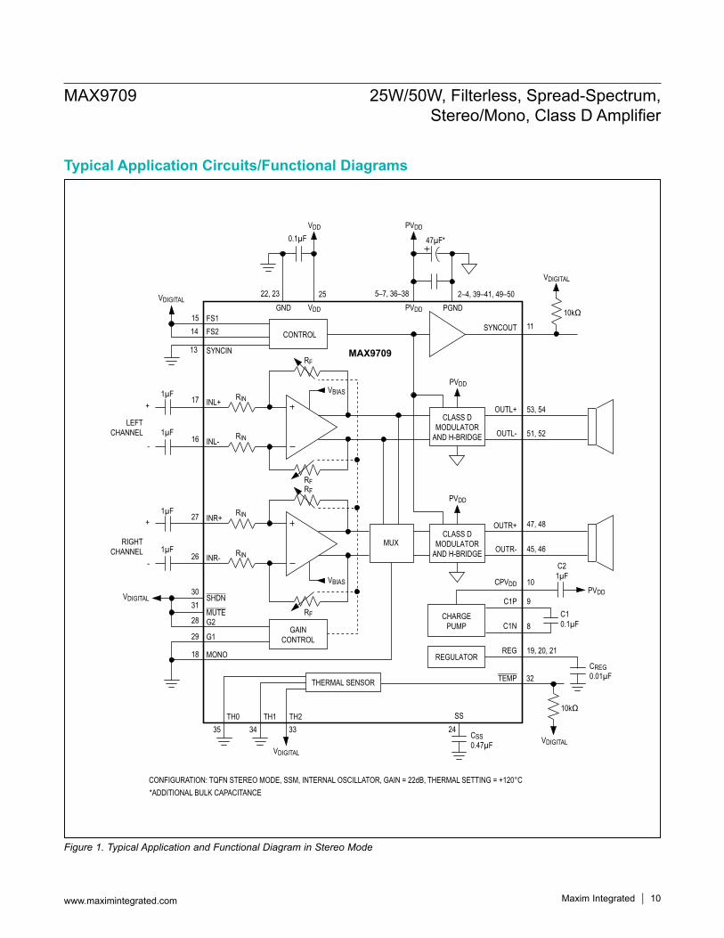
Figure 1. Typical Application and Functional Diagram in Stereo Mode
OUTR+
OUTR-
OUTL-
OUTL+
SYNCIN
INL+
INL-
INR+
INR-
SHDN
G2
G1
SYNCOUT
PGND
RIN
RIN
RIN
RIN
VBIAS
VBIAS
TH0 TH1 TH2
TEMP
CPVDDPVDD
PVDD
PVDD
PVDD
PVDD
VDD
VDD
C1P
C1N
REG
+
-
LEFTCHANNEL
+
-
RIGHTCHANNEL
VDIGITAL
C21µF
C10.1µF
0.1µF 47µF*
1µF
1µF
1µF
1µF
CREG0.01µF
CSS0.47µF VDIGITAL
VDIGITAL
VDIGITAL
VDIGITAL
GND
MONO
FS1FS2
RF
RFRF
RF
10kΩ
10kΩ
14
13
17
16
27
26
30
28
29
18
35 34 33
32
19, 20, 21
8
9
10
51, 52
53, 54
45, 46
47, 48
11
22, 23 2–4, 39–41, 49–505–7, 36–3825
15
SS24
MUTE31
*ADDITIONAL BULK CAPACITANCECONFIGURATION: TQFN STEREO MODE, SSM, INTERNAL OSCILLATOR, GAIN = 22dB, THERMAL SETTING = +120°C
MAX9709
GAINCONTROL
CONTROL
CHARGEPUMP
REGULATOR
THERMAL SENSOR
MUX
CLASS DMODULATOR
AND H-BRIDGE
CLASS DMODULATOR
AND H-BRIDGE
MAX9709 25W/50W, Filterless, Spread-Spectrum, Stereo/Mono, Class D Amplifier
www.maximintegrated.com Maxim Integrated 10
Typical Application Circuits/Functional Diagrams
Figure 2. Typical Application and Functional Diagram in Mono Mode
OUTR+
OUTR-
OUTL-
OUTL+
SYNCIN
INR+
INR-
SHDN
G1
G2
SYNCOUT
PGND
RIN
RIN
VBIAS
TH0 TH1 TH2
TEMP
CPVDDPVDD
PVDD
PVDD
PVDD
PVDD
VDD
VDD
C1P
C1N
REG
+
-
AUDIOINPUT
VDIGITAL
C21µF
0.1µF
0.1µF
47µF*
1µF
1µF
CREG0.01µF
C10.1µF
CSS0.47µF VDIGITAL
VDIGITAL
VDIGITAL
VDIGITAL
GND
MONO
FS1FS2
RF
RF
10kΩ
10kΩ
14
13
27
26
30
28
29
18
35 34 33
32
19, 20, 21
8
9
10
51, 52
53, 54
45, 46
47, 48
11
22, 23 2–4, 39–41, 49–505–7, 36–3825
15
SS24
MUTE31
VDIGITAL
MAX9709
GAINCONTROL
CHARGEPUMP
REGULATOR
THERMAL SENSOR
MUX
CONTROL
CLASS DMODULATOR
AND H-BRIDGE
CLASS DMODULATOR
AND H-BRIDGE
*ADDITIONAL BULK CAPACITANCECONFIGURATION: TQFN MONO MODE, SSM, INTERNAL OSCILLATOR, GAIN = 22dB, THERMAL SETTING = +120°C
MAX9709 25W/50W, Filterless, Spread-Spectrum, Stereo/Mono, Class D Amplifier
www.maximintegrated.com Maxim Integrated 11
Typical Application Circuits/Functional Diagrams (continued)
Detailed DescriptionThe MAX9709 filterless, Class D audio power amplifier features several improvements to switch mode ampli-fier technology. The MAX9709 is a two-channel, stereo amplifier with 25W output power on each channel. The amplifier can be configured to output 50W output power in mono mode. The device offers Class AB performance with Class D efficiency, while occupying minimal board space. A unique filterless modulation scheme and spread-spectrum switching mode create a compact, flexible, low-noise, efficient audio power amplifier. The differential input architecture reduces common-mode noise pickup, and can be used without input-coupling capacitors. The device can also be configured as a single-ended input amplifier.
Mono/Stereo ConfigurationThe MAX9709 features a mono mode that allows the right and left channels to operate in parallel, achieving up to 50W of output power. The mono mode is enabled by applying logic high to MONO. In this mode, audio signal applied to the right channel (INR+/INR-) is routed to the H-bridge of both channels, while signal applied to the left channel (INL+/INL-) is ignored. OUTL+ must be connected to OUTR+ and OUTL- must be connected to OUTR- using heavy PC board traces as close to the device as possible (see Figure 2).When the device is placed in mono mode on a PC board with outputs wired together, ensure that the MONO pin can never be driven low when the device is enabled. Driving the MONO pin low (stereo mode) while the out-puts are wired together in mono mode may trigger the short-circuit or thermal protection or both, and may even damage the device.
EfficiencyEfficiency of a Class D amplifier is attributed to the region of operation of the output stage transistors. In a Class D amplifier, the output transistors act as current-steering switches and consume negligible additional power. Any power loss associated with the Class D output stage is mostly due to the I2R loss of the MOSFET on-resistance and quiescent current overhead. The theoretical best efficiency of a linear amplifier is 78%; however, that effi-
ciency is only exhibited at peak output powers. Under nor-mal operating levels (typical music reproduction levels), efficiency falls below 30%, whereas the MAX9709 still exhibits 87% efficiency under the same conditions.
ShutdownThe MAX9709 features a shutdown mode that reduces power consumption and extends battery life. Driving SHDN low places the device in low-power (0.1µA) shut-down mode. Connect SHDN to digital high for normal operation.
Mute FunctionThe MAX9709 features a clickless/popless mute mode. When the device is muted, the outputs stop switch-ing, muting the speaker. Mute only affects the output stage and does not shut down the device. To mute the MAX9709, drive MUTE to logic low. Driving MUTE low during the power-up/down or shutdown/turn-on cycle opti-mizes click-and-pop suppression.
Click-and-Pop SuppressionThe MAX9709 features comprehensive click-and-pop suppression that eliminates audible transients on startup and shutdown. While in shutdown, the H-bridge is pulled to GND through a 330kΩ resistor. During startup or power-up, the input amplifiers are muted and an internal loop sets the modulator bias voltages to the correct levels, preventing clicks and pops when the H-bridge is subse-quently enabled. Following startup, a soft-start function gradually unmutes the input amplifiers. The value of the soft-start capacitor has an impact on the click-and-pop levels, as well as startup time.
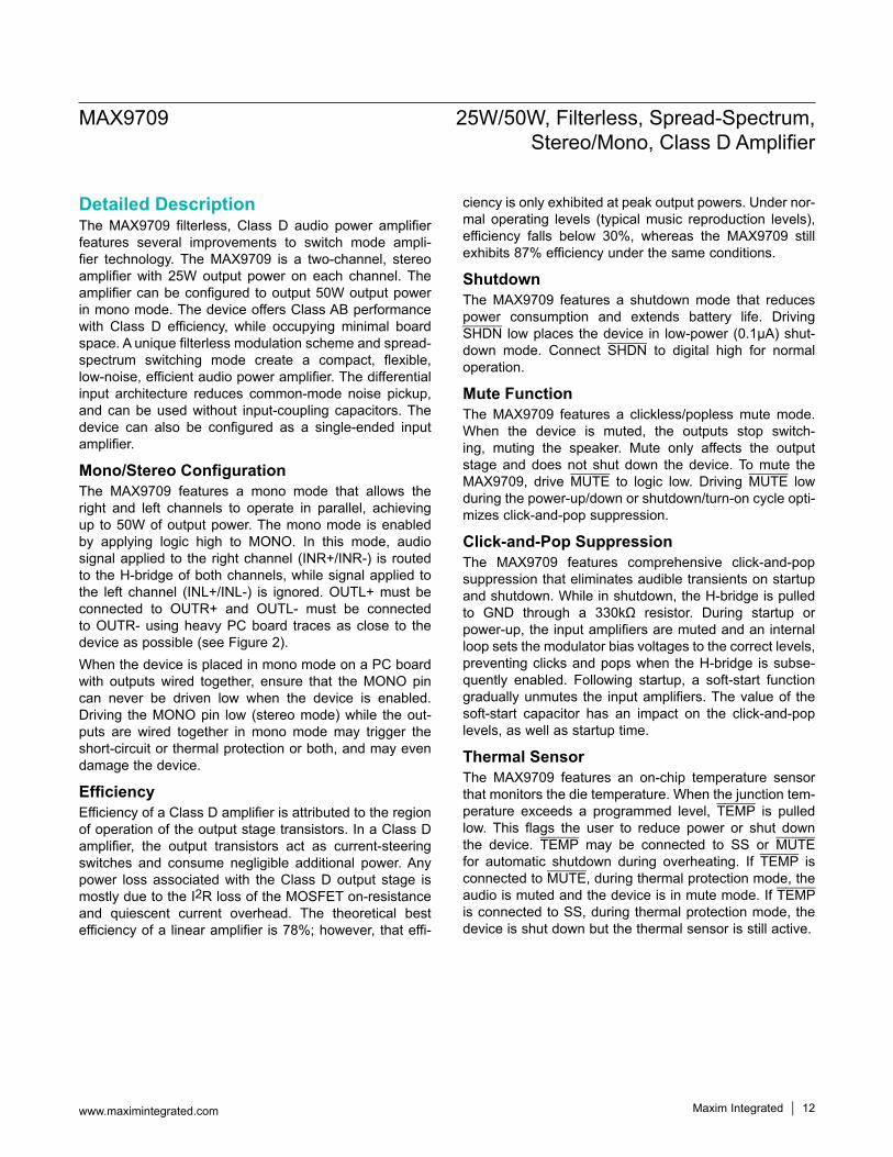
Thermal SensorThe MAX9709 features an on-chip temperature sensor that monitors the die temperature. When the junction tem-perature exceeds a programmed level, TEMP is pulled low. This flags the user to reduce power or shut down the device. TEMP may be connected to SS or MUTE for automatic shutdown during overheating. If TEMP is connected to MUTE, during thermal protection mode, the audio is muted and the device is in mute mode. If TEMP is connected to SS, during thermal protection mode, the device is shut down but the thermal sensor is still active.
MAX9709 25W/50W, Filterless, Spread-Spectrum, Stereo/Mono, Class D Amplifier
www.maximintegrated.com Maxim Integrated 12
TEMP returns high once the junction temperature cools below the set threshold minus the thermal hysteresis. If TEMP is connected to either MUTE or SS, the audio output resumes. The temperature threshold is set by the TH0, TH1, and TH2 inputs as shown in Table 1. An RC filter may be used to eliminate any transient at the TEMP output as shown in Figure 3.If TH2 = TH1 = TH0 = HIGH, it is likely that the MAX9709 enters thermal shutdown without tripping the thermal flag.
Gain SelectionThe MAX9709 features four pin-selectable gain settings; see Table 2.
Operating ModesFixed-Frequency Modulation (FFM) ModeThe MAX9709 features three switching frequencies in the FFM mode (Table 3). In this mode, the frequency spec-trum of the Class D output consists of the fundamental switching frequency and its associated harmonics (see the Wideband Output Spectrum graph in the Typical Operating Characteristics). Select one of the three fixed switching frequencies such that the harmonics do not fall in a sensitive band. The switching frequency can be changed any time without affecting audio reproduction.
Spread-Spectrum Modulation (SSM) ModeThe MAX9709 features a unique spread-spectrum (SSM) mode that flattens the wideband spectral components, improving EMI emissions that may be radiated by the speaker and cables. This mode is enabled by setting FS1 = FS2 = high. In SSM mode, the switching frequency varies randomly by ±4% around the center frequency (200kHz). The modulation scheme remains the same, but the period of the triangle waveform changes from cycle to cycle. Instead of a large amount of spectral energy pres-ent at multiples of the switching frequency, the energy is now spread over a bandwidth that increases with frequen-cy. Above a few megahertz, the wideband spectrum looks like white noise for EMI purposes. SSM mode reduces EMI compared to fixed-frequency mode. This can also help to randomize visual artifacts caused by radiated or supply borne interference in displays.
Synchronous Switching ModeThe MAX9709 SYNCIN input allows the Class D ampli-fier to switch at a frequency defined by an external clock frequency. Synchronizing the amplifier with an external clock source may confine the switching frequency to a less sensitive band. The external clock frequency range is from 600kHz to 1.2MHz and can have any duty cycle, but the minimum pulse must be greater than 100ns.SYNCOUT is an open-drain clock output for synchroniz-ing external circuitry. Its frequency is four times the ampli-fier’s switching frequency and it is active in either internal or external oscillator mode.
Figure 3. An RC Filter Eliminates Transient During Switching
Table 1. MAX9709 Junction Temperature Threshold Setting
Table 2. MAX9709 Gain SettingTable 3. Switching Frequencies
JUNCTION TEMPERATURE
(°C)TH2 TH1 TH0
80 Low Low Low
90 Low Low High
100 Low High Low
110 Low High High
120 High Low Low
129 High Low High
139 High High Low
158 High High High
G1 G2 GAIN (dB)Low High 22
High High 25
High Low 29.5
Low Low 36
FS1 FS2 SYNCOUT FREQUENCY (kHz) MODULATION
0 0 200 Fixed-frequency
0 1 250 Fixed-frequency
1 0 160 Fixed-frequency
1 1 200 ±4 Spread-spectrum
TEMP
0.1µF
10kΩ
10kΩ
VDIGITAL
TO DIGITALINPUT
MAX9709 25W/50W, Filterless, Spread-Spectrum, Stereo/Mono, Class D Amplifier
www.maximintegrated.com Maxim Integrated 13
Linear Regulator (REG)The supply voltage range for the MAX9709 is from 10V to 22V to achieve high-output power. An internal linear regu-lator reduces this voltage to 6.3V for use with small-signal and digital circuitry that does not require high-voltage sup-ply. Bypass a 0.01µF capacitor from REG to GND.
Applications InformationLogic InputsAll of the digital logic inputs and output have an absolute maximum rating of +12V. If the MAX9709 is operating with a supply voltage between 10V and 12V, digital inputs can be connected to PVDD or VDD. If PVDD and VDD are greater than 12V, digital inputs and outputs must be con-nected to a digital system supply lower than 12V.
Input AmplifierDifferential InputThe MAX9709 features a differential input structure, mak-ing them compatible with many CODECs, and offering improved noise immunity over a single-ended input ampli-fier. In devices such as flat-panel displays, noisy digital signals can be picked up by the amplifier’s inputs. These signals appear at the amplifiers’ inputs as common-mode noise. A differential input amplifier amplifies only the differ-ence of the two inputs, while any signal common to both inputs is attenuated.
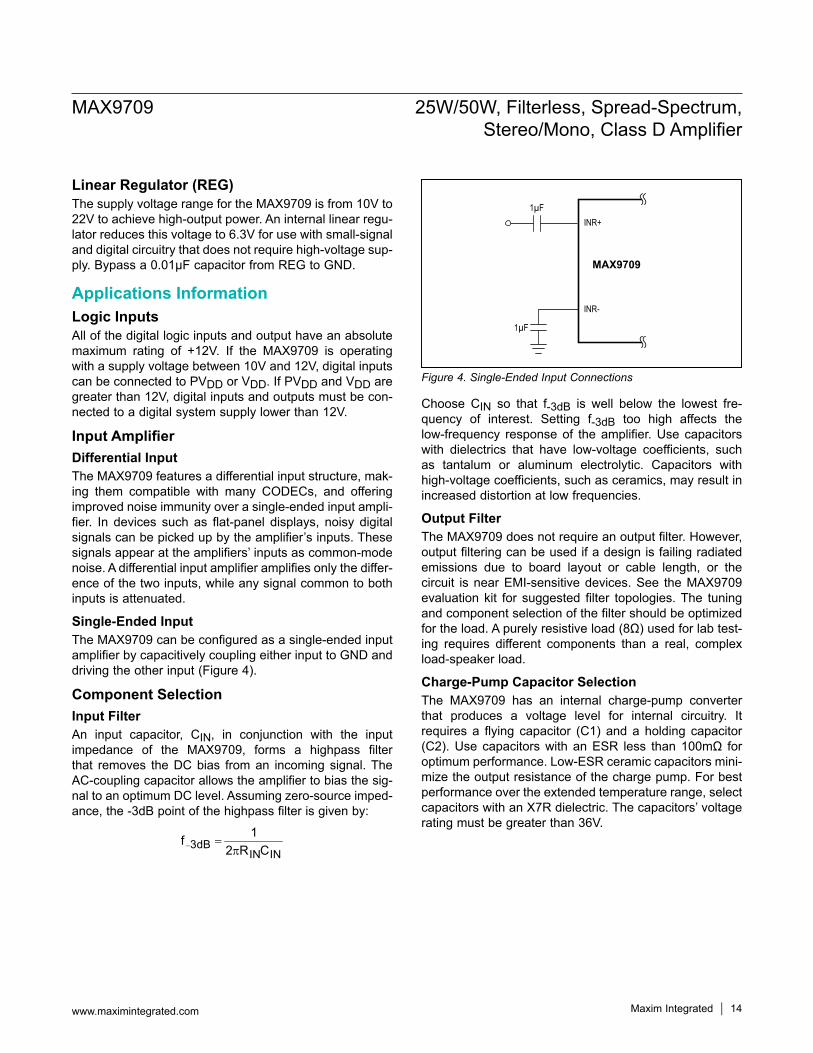
Single-Ended InputThe MAX9709 can be configured as a single-ended input amplifier by capacitively coupling either input to GND and driving the other input (Figure 4).
Component SelectionInput FilterAn input capacitor, CIN, in conjunction with the input impedance of the MAX9709, forms a highpass filter that removes the DC bias from an incoming signal. The AC-coupling capacitor allows the amplifier to bias the sig-nal to an optimum DC level. Assuming zero-source imped-ance, the -3dB point of the highpass filter is given by:
3dBIN IN
1f 2 R C− =π
Choose CIN so that f-3dB is well below the lowest fre-quency of interest. Setting f-3dB too high affects the low-frequency response of the amplifier. Use capacitors with dielectrics that have low-voltage coefficients, such as tantalum or aluminum electrolytic. Capacitors with high-voltage coefficients, such as ceramics, may result in increased distortion at low frequencies.
Output FilterThe MAX9709 does not require an output filter. However, output filtering can be used if a design is failing radiated emissions due to board layout or cable length, or the circuit is near EMI-sensitive devices. See the MAX9709 evaluation kit for suggested filter topologies. The tuning and component selection of the filter should be optimized for the load. A purely resistive load (8Ω) used for lab test-ing requires different components than a real, complex load-speaker load.
Charge-Pump Capacitor SelectionThe MAX9709 has an internal charge-pump converter that produces a voltage level for internal circuitry. It requires a flying capacitor (C1) and a holding capacitor (C2). Use capacitors with an ESR less than 100mΩ for optimum performance. Low-ESR ceramic capacitors mini-mize the output resistance of the charge pump. For best performance over the extended temperature range, select capacitors with an X7R dielectric. The capacitors’ voltage rating must be greater than 36V.
Figure 4. Single-Ended Input Connections
INR+
INR-
MAX9709
1µF
1µF
MAX9709 25W/50W, Filterless, Spread-Spectrum, Stereo/Mono, Class D Amplifier
www.maximintegrated.com Maxim Integrated 14
Sharing Input SourcesIn certain systems, a single audio source can be shared by multiple devices (speaker and headphone amplifiers). When sharing inputs, it is common to mute the unused device, rather than completely shutting it down. This pre-vents the unused device inputs from distorting the input signal. Mute the MAX9709 by driving MUTE low. Driving MUTE low turns off the Class D output stage, but does not affect the input bias levels of the MAX9709.
Frequency SynchronizationThe MAX9709 outputs up to 27W on each channel in stereo mode. If higher output power or a 2.1 solution is needed, two MAX9709s can be used. Each MAX9709 is synchronized by connecting SYNCOUT from the first MAX9709 to SYNCIN of the second MAX9709 (see Figure 5).
Supply Bypassing/LayoutProper power-supply bypassing ensures low distortion operation. For optimum performance, bypass PVDD to PGND with a 0.1µF capacitor as close to each PVDD pin as possible. A low-impedance, high-current power-supply connection to PVDD is assumed. Additional bulk capacitance should be added, as required, depending on the application and power-supply characteristics. GND and PGND should be star-connected to system ground. For the TQFN package, solder the exposed paddle (EP) to the ground plane using multiple-plated through-hole vias. The exposed paddle must be soldered to the ground plane for rated power dissipation and good ground return. Use wider PC board traces to lower the parasitic resis-tance for the high-power output pins (OUTR+, OUTR-, OUTL+, OUTL-). Refer to the MAX9709 evaluation kit for layout guidance.
Thermal ConsiderationsClass D amplifiers provide much better efficiency and thermal performance than a comparable Class AB ampli-fier. However, the system’s thermal performance must be considered with realistic expectations along with its many parameters.
Continuous Sine Wave vs. MusicWhen a Class D amplifier is evaluated in the lab, often a continuous sine wave is used as the signal source. While this is convenient for measurement purposes, it represents a worst-case scenario for thermal loading on the amplifier. It is not uncommon for a Class D amplifier to enter thermal shutdown if driven near maximum out-put power with a continuous sine wave. The PC board must be optimized for best dissipation (see the PC Board Thermal Considerations section).Audio content, both music and voice, has a much lower RMS value relative to its peak output power. Therefore, while an audio signal may reach similar peaks as a con-tinuous sine wave, the actual thermal impact on the Class D amplifier is highly reduced. If the thermal performance of a system is being evaluated, it is important to use actual audio signals instead of sine waves for testing. If sine waves must be used, the thermal performance is less than the system’s actual capability for real music or voice.
PC Board Thermal ConsiderationsThe exposed pad is the primary route for conducting heat away from the IC. With a bottom-side exposed pad, the PC board and its copper becomes the primary heatsink for the Class D amplifier. Solder the exposed pad to a copper polygon. Add as much copper as possible from this poly-gon to any adjacent pin on the Class D amplifier as well as to any adjacent components, provided these connec-tions are at the same potential. These copper paths must be as wide as possible. Each of these paths contributes to the overall thermal capabilities of the system.The copper polygon to which the exposed pad is attached should have multiple vias to the opposite side of the PC board, where they connect to another copper polygon. Make this polygon as large as possible within the sys-tem’s constraints for signal routing.Additional improvements are possible if all the traces from the device are made as wide as possible. Although the IC pins are not the primary thermal path out of the package, they do provide a small amount. The total improvement would not exceed about 10%, but it could make the difference between acceptable performance and thermal problems.
MAX9709 25W/50W, Filterless, Spread-Spectrum, Stereo/Mono, Class D Amplifier
www.maximintegrated.com Maxim Integrated 15
Auxiliary HeatsinkingIf operating in higher ambient temperatures, it is possible to improve the thermal performance of a PC board with the addition of an external heatsink. The thermal resis-tance to this heatsink must be kept as low as possible to maximize its performance. With a bottom-side exposed pad, the lowest resistance thermal path is on the bottom of the PC board. The topside of the IC is not a significant thermal path for the device, and therefore is not a cost-effective location for a heatsink. If an LC filter is used in the design, placing the inductor in close proximity to the IC can help draw heat away from the MAX9709.
Thermal CalculationsThe die temperature of a Class D amplifier can be esti-mated with some basic calculations. For example, the die temperature is calculated for the below conditions:• TA = +40°C• POUT = 16W• Efficiency (η) = 87%• θJA = 21°C/WFirst, the Class D amplifier’s power dissipation must be calculated:
OUTDISS OUT
P 16WP P 16W 2.4W0.87
− −= = =η
Then the power dissipation is used to calculate the die temperature, TC, as follows:
C A DISS JAT T P 40 C 24W 21 C / W 90.4 C= + × θ = ° + × ° = °
Load ImpedanceThe on-resistance of the MOSFET output stage in Class D amplifiers affects both the efficiency and the peak-current capability. Reducing the peak current into the load reduces the I2R losses in the MOSFETs, which increases efficiency. To keep the peak currents lower, choose the highest impedance speaker which can still deliver the desired output power within the voltage swing limits of the Class D amplifier and its supply voltage.
Another consideration is the load impedance across the audio frequency band. A loudspeaker is a complex electromechanical system with a variety of resonance. In other words, an 8Ω speaker usually has 8Ω imped-ance within a very narrow range. This often extends well below 8Ω, reducing the thermal efficiency below what is expected. This lower-than-expected impedance can be further reduced when a crossover network is used in a multidriver audio system.
Systems Application CircuitThe MAX9709 can be configured into multiple amplifier systems. One concept is a 2.1 audio system (Figure 5) where a stereo audio source is split into three channels. The left- and right-channel inputs are highpass filtered to remove the bass content, and then amplified by the MAX9709 in stereo mode. Also, the left- and right-channel inputs are summed together and lowpass filtered to remove the high-frequency content, then amplified by a second MAX9709 in mono mode.The conceptual drawing of Figure 5 can be applied to either single-ended or differential systems. Figure 6 illustrates the circuitry required to implement a fully differential filtering system. By maintaining a fully differ-ential path, the signal-to-noise ratio remains uncompro-mised and noise pickup is kept very low. However, keep-ing a fully differential signal path results in almost twice the component count, and therefore performance must be weighed against cost and size.The highpass and lowpass filters should have different cutoff frequencies to ensure an equal power response at the crossover frequency. The filters should be at -6dB amplitude at the crossover frequency, which is known as a Linkwitz-Riley alignment. In the example cir-cuit of Figure 6, the -3dB cutoff frequency for the highpass filters is 250Hz, and the -3dB cutoff frequency for the lowpass filter is 160Hz. Both the highpass filters and the lowpass filters are at a -6dB amplitude at approximately 200Hz. If the filters were to have the same -3dB cutoff fre-quency, a measurement of sound pressure level (SPL) vs. frequency would have a peak at the crossover frequency.
MAX9709 25W/50W, Filterless, Spread-Spectrum, Stereo/Mono, Class D Amplifier
www.maximintegrated.com Maxim Integrated 16

The circuit in Figure 6 uses inverting amplifiers for their ease in biasing. Note the phase labeling at the outputs has been reversed. The resistors should be 1% or better in tolerance and the capacitors 5% tolerance or better. Mismatch in the components can cause discrepancies between the nominal transfer function and actual perfor-mance. Also, the mismatch of the input resistors (R15, R17, R19, and R21 in Figure 6) of the summing amplifier and lowpass filter causes some high-frequency sound to be sent to the subwoofer.
The circuit in Figure 6 drives a pair of MAX9709 devic-es similar to the circuit in Figure 5. The inputs to the MAX9709 still require AC-coupling to prevent compromis-ing the click-and-pop performance of the MAX9709.The left and right drivers should be at an 8Ω to 12Ω imped-ance, whereas the subwoofer can be 4Ω to 8Ω depending on the desired output power, the available power-supply voltage, and the sensitivity of the individual speakers in the system. The four gain settings of the MAX9709 allow gain adjustments to match the sensitivity of the speakers.
Figure 5. Multiple Amplifiers Implement a 2.1 Audio System
MAX9709
MAX9709
HIGHPASSFILTER
8ΩFULL-RANGESPEAKER
8ΩFULL-RANGESPEAKER
4Ω OR 8ΩWOOFER
RIGHTAUDIO
LEFTAUDIO
HIGHPASSFILTER
LOWPASSFILTER∑
VDIGITAL
OUTR+OUTR-
OUTL+OUTL-
OUTR+OUTR-
OUTL+OUTL-
INR+INR-
MONO
INL+INL-
INR+
SYNCIN
SYNCOUT
INR-
MONO
INL+
INL-
MAX9709 25W/50W, Filterless, Spread-Spectrum, Stereo/Mono, Class D Amplifier
www.maximintegrated.com Maxim Integrated 17
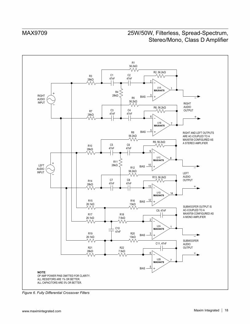
Figure 6. Fully Differential Crossover Filters
BIAS
2
3
1
C1 47nF
R328kΩ
R2, 56.2kΩ
R156.2kΩ
C2 47nF
MAX4478U1A
BIAS
6
5
7
C3 47nF
R728kΩ
R6, 56.2kΩRIGHTAUDIOOUTPUT
RIGHTAUDIOINPUT
R556.2kΩ
R428kΩ
C4 47nF
MAX4478U1B
BIAS
9
10
8
C547nF
R1028kΩ
R9, 56.2kΩ
R856.2kΩ
C6 47nF
MAX4478U1C
BIAS
13
12
14
C7 47nF
R1428kΩ
R13, 56.2kΩLEFTAUDIOOUTPUT
SUBWOOFER OUTPUT ISAC-COUPLED TO AMAX9709 CONFIGURED ASA MONO AMPLIFIER
NOTE:OP AMP POWER PINS OMITTED FOR CLARITY.ALL RESISTORS ARE 1% OR BETTER.ALL CAPACITORS ARE 5% OR BETTER.
RIGHT AND LEFT OUTPUTSARE AC-COUPLED TO AMAX9709 CONFIGURED ASA STEREO AMPLIFIER
SUBWOOFERAUDIOOUTPUT
LEFTAUDIOINPUT
R1256.2kΩ
R1128kΩ
C8 47nF
MAX4478U1D
BIAS
2
3
1
R1726.1kΩ
R1526.1kΩ
MAX4478U2A
R1613kΩ
C9, 47nF
C1047nF
R187.5kΩ
BIAS
6
5
7
R2128kΩ
R1926.1kΩ
MAX4478U2B
R2013kΩ
C11, 47nFR22
7.5kΩ
MAX9709 25W/50W, Filterless, Spread-Spectrum, Stereo/Mono, Class D Amplifier
www.maximintegrated.com Maxim Integrated 18
PACKAGE TYPE
PACKAGE CODE OUTLINE NO.
LAND PATTERN
NO.
56 TQFN-EP T5688-3 21-0135 90-0047
TOP VIEW
PGND
PGND
PGND
PVDD
PVDD
PVDD
TH0
TH1
TH2
G2
TEMP
MUTE
SHDN
N.C.
36
37
38
39
40
32
33
34
35
41
18 19 20 21 22 23 24 25 26 27
OUTL
+
THIN QFN
30
31
29
INR+
INR-V D
DSSGND
GND
REG
REG
REG
FS1
15 16 17
MONOINL+
INL-
OUTL
-
OUTL
-PG
ND
PGND
OUTR
+
N.C.
N.C.
OUTL
+
OUTR
+
OUTR
-
OUTR
-
N.C.
28
G1N.
C.
SYNCOUT
CPVDD
C1P
C1N
PVDD
PVDD
FS2
SYNCIN
N.C.
PVDD
PGND
PGND
PGND
N.C. 42
7
6
5
4
3
11
10
9
8
2
13
12
14
1
53 52 51 50 49 48 47 46 45 4456 55 54 43
MAX9709
+
MAX9709 25W/50W, Filterless, Spread-Spectrum, Stereo/Mono, Class D Amplifier
www.maximintegrated.com Maxim Integrated 19
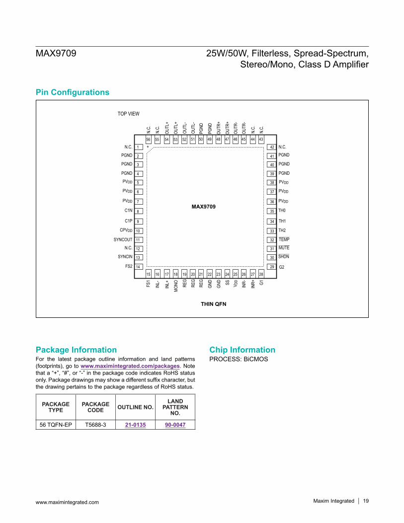
Pin Configurations
Chip InformationPROCESS: BiCMOS
Package InformationFor the latest package outline information and land patterns (footprints), go to www.maximintegrated.com/packages. Note that a “+”, “#”, or “-” in the package code indicates RoHS status only. Package drawings may show a different suffix character, but the drawing pertains to the package regardless of RoHS status.
REVISION NUMBER
REVISION DATE DESCRIPTION PAGES
CHANGED
0 9/05 Initial release —
1 5/08 Removed TQFP package 1, 2, 8–11, 20
2 5/14 Removed automotive reference from Applications section 1
Maxim Integrated cannot assume responsibility for use of any circuitry other than circuitry entirely embodied in a Maxim Integrated product. No circuit patent licenses are implied. Maxim Integrated reserves the right to change the circuitry and specifications without notice at any time. The parametric values (min and max limits) shown in the Electrical Characteristics table are guaranteed. Other parametric values quoted in this data sheet are provided for guidance.
Maxim Integrated and the Maxim Integrated logo are trademarks of Maxim Integrated Products, Inc.
MAX9709 25W/50W, Filterless, Spread-Spectrum, Stereo/Mono, Class D Amplifier
© 2014 Maxim Integrated Products, Inc. 20
Revision History
For pricing, delivery, and ordering information, please contact Maxim Direct at 1-888-629-4642, or visit Maxim Integrated’s website at www.maximintegrated.com.