TPH2501/TPH2502/TPH2503 /TPH2504 3 P E A K 250MHz...
20
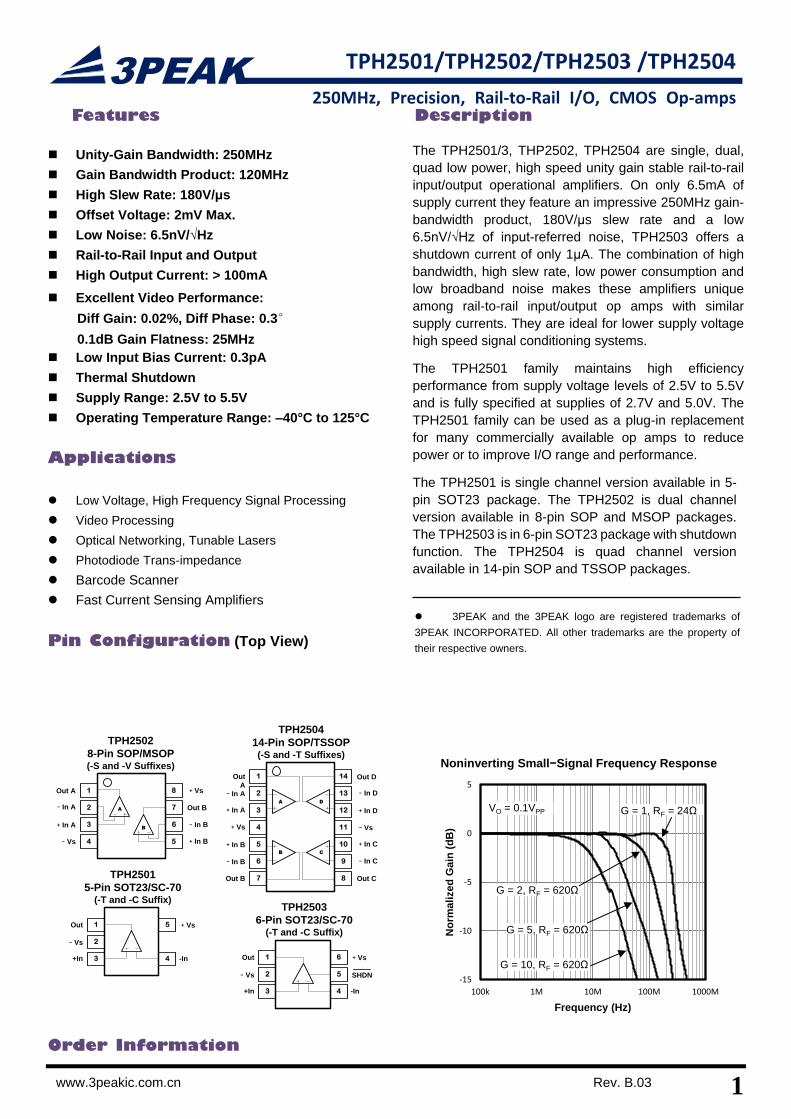
3PEAK 1 TPH2501/TPH2502/TPH2503 /TPH2504 250MHz, Precision, Rail-to-Rail I/O, CMOS Op-amps www.3peakic.com.cn Rev. B.03 Features Unity-Gain Bandwidth: 250MHz Gain Bandwidth Product: 120MHz High Slew Rate: 180V/μs Offset Voltage: 2mV Max. Low Noise: 6.5nV/√Hz Rail-to-Rail Input and Output High Output Current: > 100mA Excellent Video Performance: Diff Gain: 0.02%, Diff Phase: 0.3° 0.1dB Gain Flatness: 25MHz Low Input Bias Current: 0.3pA Thermal Shutdown Supply Range: 2.5V to 5.5V Operating Temperature Range: –40°C to 125°C Applications Low Voltage, High Frequency Signal Processing Video Processing Optical Networking, Tunable Lasers Photodiode Trans-impedance Barcode Scanner Fast Current Sensing Amplifiers Pin Configuration (Top View) TPH2502 8-Pin SOP/MSOP (-S and -V Suffixes) 8 6 5 7 3 2 1 4 Out A ﹢In A ﹣In A ﹢In B ﹣In B Out B A B ﹣Vs ﹢Vs TPH2501 5-Pin SOT23/SC-70 (-T and -C Suffix) 4 5 3 2 1 Out +In -In ﹣Vs ﹢Vs TPH2504 14-Pin SOP/TSSOP (-S and -T Suffixes) 14 13 12 11 10 9 8 6 5 7 3 2 1 4 Out A ﹢In A ﹣In A D A C B Out D ﹢In D ﹣In D Out B ﹢In B ﹣In B Out C ﹢In C ﹣In C ﹣Vs ﹢Vs TPH2503 6-Pin SOT23/SC-70 (-T and -C Suffix) 4 6 3 2 1 Out +In -In ﹣Vs ﹢Vs 5 SHDN Description The TPH2501/3, THP2502, TPH2504 are single, dual, quad low power, high speed unity gain stable rail-to-rail input/output operational amplifiers. On only 6.5mA of supply current they feature an impressive 250MHz gain- bandwidth product, 180V/μs slew rate and a low 6.5nV/√Hz of input-referred noise, TPH2503 offers a shutdown current of only 1μA. The combination of high bandwidth, high slew rate, low power consumption and low broadband noise makes these amplifiers unique among rail-to-rail input/output op amps with similar supply currents. They are ideal for lower supply voltage high speed signal conditioning systems. The TPH2501 family maintains high efficiency performance from supply voltage levels of 2.5V to 5.5V and is fully specified at supplies of 2.7V and 5.0V. The TPH2501 family can be used as a plug-in replacement for many commercially available op amps to reduce power or to improve I/O range and performance. The TPH2501 is single channel version available in 5- pin SOT23 package. The TPH2502 is dual channel version available in 8-pin SOP and MSOP packages. The TPH2503 is in 6-pin SOT23 package with shutdown function. The TPH2504 is quad channel version available in 14-pin SOP and TSSOP packages. 3PEAK and the 3PEAK logo are registered trademarks of 3PEAK INCORPORATED. All other trademarks are the property of their respective owners. Noninverting Small−Signal Frequency Response Order Information -15 -10 -5 0 5 100k 1M 10M 100M 1000M Normalized Gain (dB) Frequency (Hz) G = 1, R F = 24Ω G = 2, R F = 620Ω G = 5, R F = 620Ω G = 10, R F = 620Ω V O = 0.1V PP
Transcript of TPH2501/TPH2502/TPH2503 /TPH2504 3 P E A K 250MHz...
3PEAK
1
TPH2501/TPH2502/TPH2503 /TPH2504
250MHz, Precision, Rail-to-Rail I/O, CMOS Op-amps
www.3peakic.com.cn Rev. B.03
Features
Unity-Gain Bandwidth: 250MHz
Gain Bandwidth Product: 120MHz
High Slew Rate: 180V/μs
Offset Voltage: 2mV Max.
Low Noise: 6.5nV/√Hz
Rail-to-Rail Input and Output
High Output Current: > 100mA
Excellent Video Performance:
Diff Gain: 0.02%, Diff Phase: 0.3°
0.1dB Gain Flatness: 25MHz
Low Input Bias Current: 0.3pA
Thermal Shutdown
Supply Range: 2.5V to 5.5V
Operating Temperature Range: –40°C to 125°C
Applications
Low Voltage, High Frequency Signal Processing
Video Processing
Optical Networking, Tunable Lasers
Photodiode Trans-impedance
Barcode Scanner
Fast Current Sensing Amplifiers
Pin Configuration (Top View)
TPH2502
8-Pin SOP/MSOP(-S and -V Suffixes)
8
6
5
7
3
2
1
4
Out A
﹢In A
﹣In A
﹢In B
﹣In B
Out BA
B
﹣Vs
﹢Vs
TPH2501
5-Pin SOT23/SC-70(-T and -C Suffix)
4
5
3
2
1Out
+In -In
﹣Vs
﹢Vs
TPH2504
14-Pin SOP/TSSOP(-S and -T Suffixes)
14
13
12
11
10
9
8
6
5
7
3
2
1
4
Out
A
﹢In A
﹣In ADA
CB
Out D
﹢In D
﹣In D
Out B
﹢In B
﹣In B
Out C
﹢In C
﹣In C
﹣Vs﹢Vs
TPH2503
6-Pin SOT23/SC-70(-T and -C Suffix)
4
6
3
2
1Out
+In -In
﹣Vs
﹢Vs
5 SHDN
Description
The TPH2501/3, THP2502, TPH2504 are single, dual,
quad low power, high speed unity gain stable rail-to-rail
input/output operational amplifiers. On only 6.5mA of
supply current they feature an impressive 250MHz gain-
bandwidth product, 180V/μs slew rate and a low
6.5nV/√Hz of input-referred noise, TPH2503 offers a
shutdown current of only 1μA. The combination of high
bandwidth, high slew rate, low power consumption and
low broadband noise makes these amplifiers unique
among rail-to-rail input/output op amps with similar
supply currents. They are ideal for lower supply voltage
high speed signal conditioning systems.
The TPH2501 family maintains high efficiency
performance from supply voltage levels of 2.5V to 5.5V
and is fully specified at supplies of 2.7V and 5.0V. The
TPH2501 family can be used as a plug-in replacement
for many commercially available op amps to reduce
power or to improve I/O range and performance.
The TPH2501 is single channel version available in 5-
pin SOT23 package. The TPH2502 is dual channel
version available in 8-pin SOP and MSOP packages.
The TPH2503 is in 6-pin SOT23 package with shutdown
function. The TPH2504 is quad channel version
available in 14-pin SOP and TSSOP packages.
3PEAK and the 3PEAK logo are registered trademarks of
3PEAK INCORPORATED. All other trademarks are the property of
their respective owners.
Noninverting Small−Signal Frequency Response
Order Information
-15
-10
-5
0
5
100k 1M 10M 100M 1000M
No
rmalized
Gain
(d
B)
Frequency (Hz)
G = 1, RF = 24Ω
G = 2, RF = 620Ω
G = 5, RF = 620Ω
G = 10, RF = 620Ω
VO = 0.1VPP
2 Rev. B.03 www.3peakic.com.cn
TPH2501/TPH2502/TPH2503/TPH2504
250MHz, Precision, Rail-to-Rail I/O, CMOS Op-amps
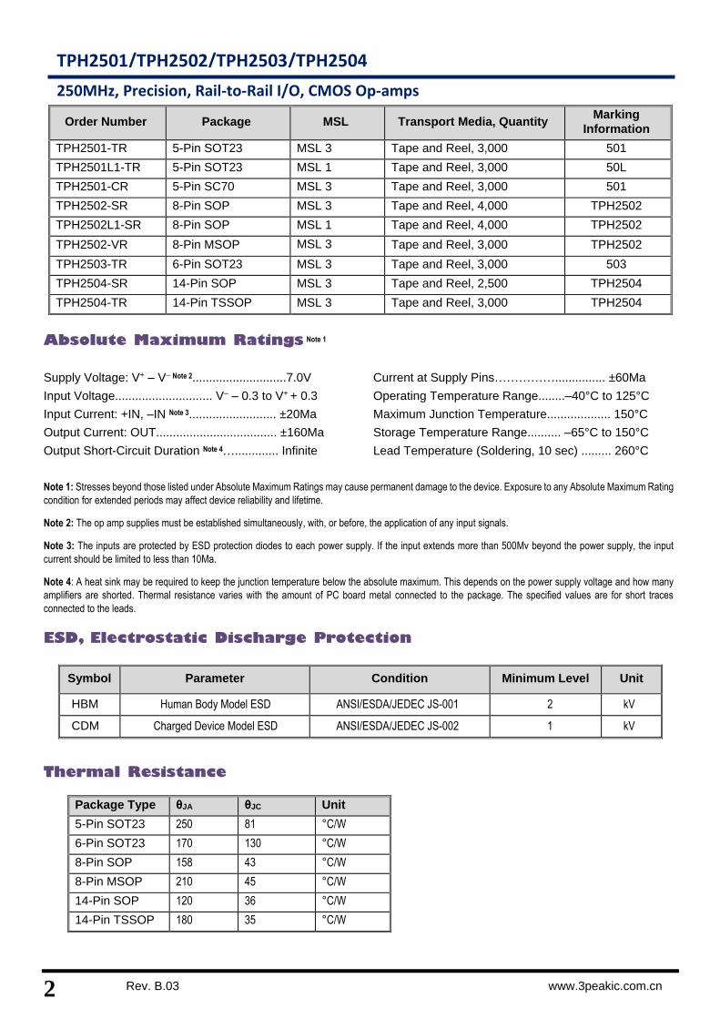
Order Number Package MSL Transport Media, Quantity Marking
Information
TPH2501-TR 5-Pin SOT23 MSL 3 Tape and Reel, 3,000 501
TPH2501L1-TR 5-Pin SOT23 MSL 1 Tape and Reel, 3,000 50L
TPH2501-CR 5-Pin SC70 MSL 3 Tape and Reel, 3,000 501
TPH2502-SR 8-Pin SOP MSL 3 Tape and Reel, 4,000 TPH2502
TPH2502L1-SR 8-Pin SOP MSL 1 Tape and Reel, 4,000 TPH2502
TPH2502-VR 8-Pin MSOP MSL 3 Tape and Reel, 3,000 TPH2502
TPH2503-TR 6-Pin SOT23 MSL 3 Tape and Reel, 3,000 503
TPH2504-SR 14-Pin SOP MSL 3 Tape and Reel, 2,500 TPH2504
TPH2504-TR 14-Pin TSSOP MSL 3 Tape and Reel, 3,000 TPH2504
Absolute Maximum Ratings Note 1
Supply Voltage: V+ – V– Note 2............................7.0V
Input Voltage............................. V– – 0.3 to V+ + 0.3
Input Current: +IN, –IN Note 3.......................... ±20Ma
Output Current: OUT.................................... ±160Ma
Output Short-Circuit Duration Note 4…............. Infinite
Current at Supply Pins……………............... ±60Ma
Operating Temperature Range........–40°C to 125°C
Maximum Junction Temperature................... 150°C
Storage Temperature Range.......... –65°C to 150°C
Lead Temperature (Soldering, 10 sec) ......... 260°C
Note 1: Stresses beyond those listed under Absolute Maximum Ratings may cause permanent damage to the device. Exposure to any Absolute Maximum Rating
condition for extended periods may affect device reliability and lifetime.
Note 2: The op amp supplies must be established simultaneously, with, or before, the application of any input signals.
Note 3: The inputs are protected by ESD protection diodes to each power supply. If the input extends more than 500Mv beyond the power supply, the input
current should be limited to less than 10Ma.
Note 4: A heat sink may be required to keep the junction temperature below the absolute maximum. This depends on the power supply voltage and how many
amplifiers are shorted. Thermal resistance varies with the amount of PC board metal connected to the package. The specified values are for short traces
connected to the leads.
ESD, Electrostatic Discharge Protection
Symbol Parameter Condition Minimum Level Unit
HBM Human Body Model ESD ANSI/ESDA/JEDEC JS-001 2 kV
CDM Charged Device Model ESD ANSI/ESDA/JEDEC JS-002 1 kV
Thermal Resistance
Package Type θJA θJC Unit
5-Pin SOT23 250 81 ° C/W
6-Pin SOT23 170 130 ° C/W
8-Pin SOP 158 43 ° C/W
8-Pin MSOP 210 45 ° C/W
14-Pin SOP 120 36 ° C/W
14-Pin TSSOP 180 35 ° C/W
3
TPH2501/TPH2502/TPH2503/TPH2504
250MHz, Precision, Rail-to-Rail I/O, CMOS
Op-amps
www.3peakic.com.cn Rev. B.03
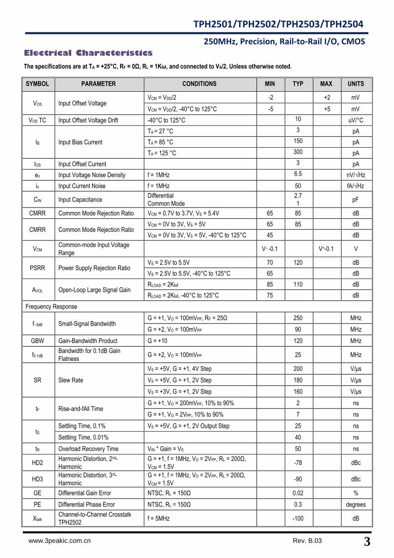
Electrical Characteristics
The specifications are at TA = +25° C, RF = 0Ω, RL = 1Kω, and connected to VS/2, Unless otherwise noted.
SYMBOL PARAMETER CONDITIONS MIN TYP MAX UNITS
VOS Input Offset Voltage VCM = VDD/2 -2 +2 mV
VCM = VDD/2, -40° C to 125° C -5 +5 mV
VOS TC Input Offset Voltage Drift -40° C to 125° C 10 uV/° C
IB Input Bias Current
TA = 27 ° C 3 pA
TA = 85 ° C 150 pA
TA = 125 ° C 300 pA
IOS Input Offset Current 3 pA
en Input Voltage Noise Density f = 1MHz 6.5 nV/√Hz
in Input Current Noise f = 1MHz 50 fA/√Hz
CIN Input Capacitance Differential
Common Mode
2.7
1 pF
CMRR Common Mode Rejection Ratio VCM = 0.7V to 3.7V, VS = 5.4V 65 85 dB
CMRR Common Mode Rejection Ratio VCM = 0V to 3V, VS = 5V 65 85 dB
VCM = 0V to 3V, VS = 5V, -40° C to 125° C 45 dB
VCM Common-mode Input Voltage
Range V– -0.1 V+-0.1 V
PSRR Power Supply Rejection Ratio VS = 2.5V to 5.5V 70 120 dB
VS = 2.5V to 5.5V, -40° C to 125° C 65 dB
AVOL Open-Loop Large Signal Gain RLOAD = 2Kω 85 110 dB
RLOAD = 2Kω, -40° C to 125° C 75 dB
Frequency Response
f−3dB Small-Signal Bandwidth G = +1, VO = 100mVPP, RF = 25Ω 250 MHz
G = +2, VO = 100mVPP 90 MHz
GBW Gain-Bandwidth Product G = +10 120 MHz
f0.1dB Bandwidth for 0.1dB Gain
Flatness G = +2, VO = 100mVPP 25 MHz
SR Slew Rate
VS = +5V, G = +1, 4V Step 200 V/μs
VS = +5V, G = +1, 2V Step 180 V/μs
VS = +3V, G = +1, 2V Step 160 V/μs
tF Rise-and-fAll Time G = +1, VO = 200mVPP, 10% to 90% 2 ns
G = +1, VO = 2VPP, 10% to 90% 7 ns
tS Settling Time, 0.1% VS = +5V, G = +1, 2V Output Step 25 ns
Settling Time, 0.01% 40 ns
tR Overload Recovery Time VIN * Gain = VS 50 ns
HD2 Harmonic Distortion, 2nd-
Harmonic
G = +1, f = 1MHz, VO = 2VPP, RL = 200Ω,
VCM = 1.5V -78 dBc
HD3 Harmonic Distortion, 3rd-
Harmonic
G = +1, f = 1MHz, VO = 2VPP, RL = 200Ω,
VCM = 1.5V -90 dBc
GE Differential Gain Error NTSC, RL = 150Ω 0.02 %
PE Differential Phase Error NTSC, RL = 150Ω 0.3 degrees
Xtalk Channel-to-Channel Crosstalk
TPH2502 f = 5MHz -100 dB
4 Rev. B.03 www.3peakic.com.cn
TPH2501/TPH2502/TPH2503/TPH2504
250MHz, Precision, Rail-to-Rail I/O, CMOS Op-amps
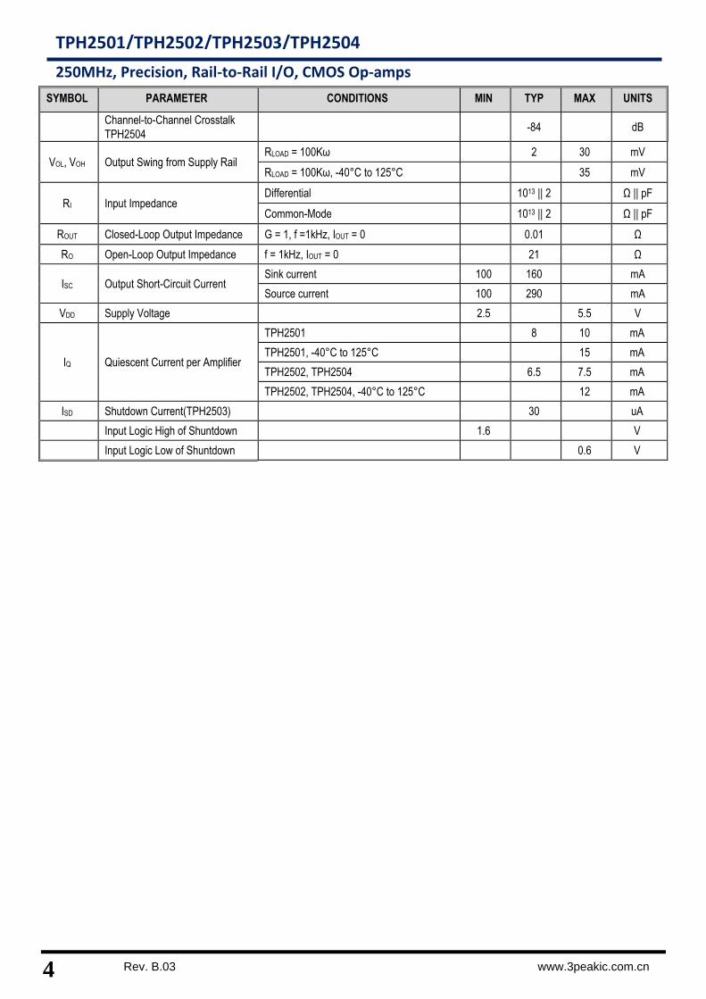
SYMBOL PARAMETER CONDITIONS MIN TYP MAX UNITS
Channel-to-Channel Crosstalk
TPH2504 -84 dB
VOL, VOH Output Swing from Supply Rail RLOAD = 100Kω 2 30 mV
RLOAD = 100Kω, -40° C to 125° C 35 mV
RI Input Impedance Differential 1013 || 2 Ω || pF
Common-Mode 1013 || 2 Ω || pF
ROUT Closed-Loop Output Impedance G = 1, f =1kHz, IOUT = 0 0.01 Ω
RO Open-Loop Output Impedance f = 1kHz, IOUT = 0 21 Ω
ISC Output Short-Circuit Current Sink current 100 160 mA
Source current 100 290 mA
VDD Supply Voltage 2.5 5.5 V
IQ Quiescent Current per Amplifier
TPH2501 8 10 mA
TPH2501, -40° C to 125° C 15 mA
TPH2502, TPH2504 6.5 7.5 mA
TPH2502, TPH2504, -40° C to 125° C 12 mA
ISD Shutdown Current(TPH2503) 30 uA
Input Logic High of Shuntdown 1.6 V
Input Logic Low of Shuntdown 0.6 V
5
TPH2501/TPH2502/TPH2503/TPH2504
250MHz, Precision, Rail-to-Rail I/O, CMOS
Op-amps
www.3peakic.com.cn Rev. B.03
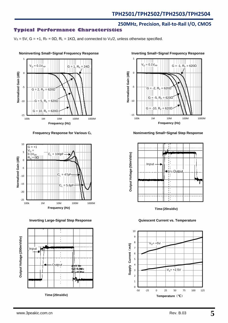
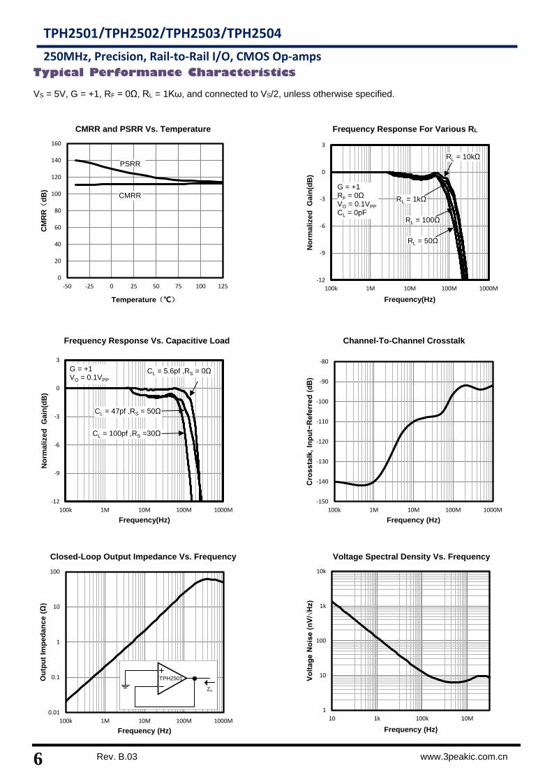
Typical Performance Characteristics
VS = 5V, G = +1, RF = 0Ω, RL = 1KΩ, and connected to VS/2, unless otherwise specified.
Noninverting Small−Signal Frequency Response Inverting Small−Signal Frequency Response
Frequency Response for Various CL Noninverting Small−Signal Step Response
Inverting Large-Signal Step Response Quiescent Current vs. Temperature
-15
-10
-5
0
5
100k 1M 10M 100M 1000M
No
rmalized
Gain
(d
B)
Frequency (Hz)
G = 1, RF = 24Ω
G = 2, RF = 620Ω
G = 5, RF = 620Ω
G = 10, RF = 620Ω
VO = 0.1VPP
-15
-10
-5
0
5
100k 1M 10M 100M 1000M
No
rmalized
Gain
(d
B)
Frequency (Hz)
G = -1, RF = 620Ω
G = -2, RF = 620Ω
G = -5, RF = 620Ω
G = -10, RF = 620Ω
VO = 0.1VPP
-25
-20
-15
-10
-5
0
5
10
100k 1M 10M 100M 1000M
No
rmalized
Gain
(d
B)
Frequency (Hz)
CL = 47pF
CL = 5.6pF
CL = 100pF
G = +1VO = 0.1VPP
RS = 0Ω
Time (20ns/div)
Ou
tpu
t V
olt
ag
e (50m
V/d
iv)
Input
Output
Time (20ns/div)
Ou
tpu
t V
olt
ag
e (200m
V/d
iv)
Input
Output
0
1
2
3
4
5
6
7
8
9
10
-50 -25 0 25 50 75 100 125
Su
pp
ly
Cu
rren
t(m
A)
Temperature(℃)
VS= +5V
VS= +2.5V
6 Rev. B.03 www.3peakic.com.cn
TPH2501/TPH2502/TPH2503/TPH2504
250MHz, Precision, Rail-to-Rail I/O, CMOS Op-amps
Typical Performance Characteristics
VS = 5V, G = +1, RF = 0Ω, RL = 1Kω, and connected to VS/2, unless otherwise specified.
CMRR and PSRR Vs. Temperature Frequency Response For Various RL
Frequency Response Vs. Capacitive Load Channel-To-Channel Crosstalk
Closed-Loop Output Impedance Vs. Frequency Voltage Spectral Density Vs. Frequency
0
20
40
60
80
100
120
140
160
-50 -25 0 25 50 75 100 125
CM
RR(
dB
)
Temperature(℃)
CMRR
PSRR
-12
-9
-6
-3
0
3
100k 1M 10M 100M 1000M
No
rmalized
G
ain
(dB
)
Frequency(Hz)
RL = 10kΩ
RL = 1kΩ
RL = 100Ω
RL = 50Ω
G = +1RF = 0ΩVO = 0.1VPP
CL = 0pF
-12
-9
-6
-3
0
3
100k 1M 10M 100M 1000M
No
rmalized
G
ain
(dB
)
Frequency(Hz)
CL = 5.6pf ,RS = 0Ω
CL = 100pf ,RS =30Ω
CL = 47pf ,RS = 50Ω
G = +1VO = 0.1VPP
-150
-140
-130
-120
-110
-100
-90
-80
100k 1M 10M 100M 1000M
Cro
ssta
lk,
Inp
ut−
Refe
rred
(d
B)
Frequency (Hz)
0.01
0.1
1
10
100
100k 1M 10M 100M 1000M
Ou
tpu
t Im
ped
an
ce (
Ω)
Frequency (Hz)
TPH2501
Zo
1
10
100
1k
10k
10 1k 100k 10M
Vo
ltag
e N
ois
e (
nV
/√H
z)
Frequency (Hz)
7
TPH2501/TPH2502/TPH2503/TPH2504
250MHz, Precision, Rail-to-Rail I/O, CMOS
Op-amps
www.3peakic.com.cn Rev. B.03
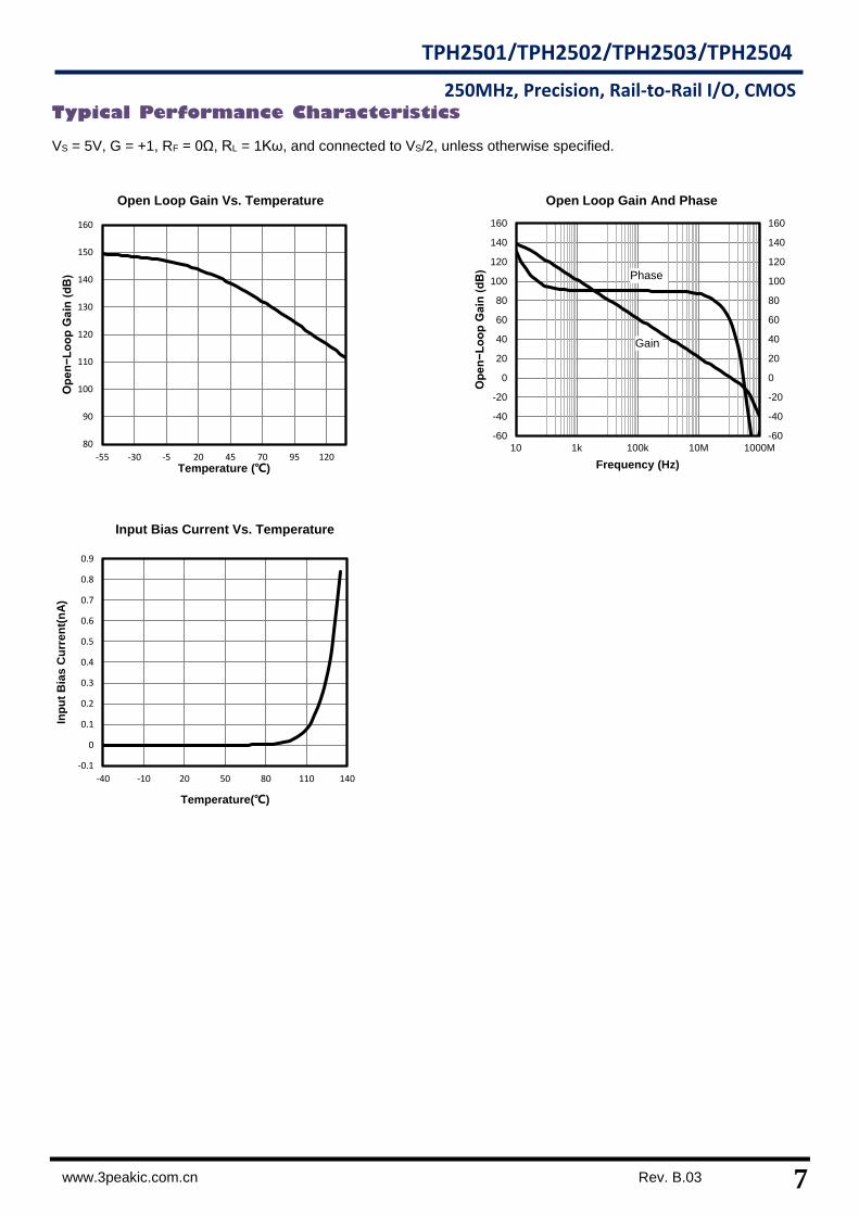
Typical Performance Characteristics
VS = 5V, G = +1, RF = 0Ω, RL = 1Kω, and connected to VS/2, unless otherwise specified.
Open Loop Gain Vs. Temperature Open Loop Gain And Phase
Input Bias Current Vs. Temperature
80
90
100
110
120
130
140
150
160
-55 -30 -5 20 45 70 95 120
Op
en
−L
oo
p G
ain
(d
B)
Temperature (℃)
-60
-40
-20
0
20
40
60
80
100
120
140
160
-60
-40
-20
0
20
40
60
80
100
120
140
160
10 1k 100k 10M 1000M
Op
en
−L
oo
p G
ain
(d
B)
Frequency (Hz)
Phase
Gain
-0.1
0
0.1
0.2
0.3
0.4
0.5
0.6
0.7
0.8
0.9
-40 -10 20 50 80 110 140
Inp
ut
Bia
s C
urr
en
t(n
A)
Temperature(℃)
8 Rev. B.03 www.3peakic.com.cn
TPH2501/TPH2502/TPH2503/TPH2504
250MHz, Precision, Rail-to-Rail I/O, CMOS Op-amps
Pin Functions
-IN: Inverting Input of the Amplifier.
+IN: Non-Inverting Input of Amplifier.
OUT: Amplifier Output. The voltage range extends to
within Mv of each supply rail.
V+ or +Vs: Positive Power Supply. Typically the voltage
is from 2.5V to 5.5V. Split supplies are possible as long
as the voltage between V+ and V– is between 2.5V and
5.5V. A bypass capacitor of 0.1Μf as close to the part as
possible should be used between power supply pins or
between supply pins and ground.
V- or –Vs: Negative Power Supply. It is normally tied to
ground. It can also be tied to a voltage other than ground
as long as the voltage between V+ and V– is from 2.5V to
5.5V. If it is not connected to ground, bypass it with a
capacitor of 0.1Μf as close to the part as possible.
SHDN: High on this pin logic low to shut down the
device. Range: Logic high enables the device and logic
low shut down the device. This pin defaults to logic
high if left open.
Operation
The TPH2501,TPH2502,TPH2504 is a CMOS, rail-to-rail I/O, high-speed, voltage-feedback operational amplifier
designed for video, high-speed, and other applications. It is available as a single, dual, or quad op amp. The amplifier
features a 250MHz gain bandwidth, and 180V/μs slew rate, but it is unity-gain stable and can be operated as a +1V/V
voltage follower. The TPH2501/TPH2502/TPH2504 is specified over a power-supply range of +2.7V to +5.5V (±1.35V
to ±2.75V). However, the supply voltage may range from +2.5V to +5.5V (±1.25V to ±2.75V). Supply voltages higher
than 7.5V (absolute maximum) can permanently damage the amplifier. Parameters that vary over supply voltage or
temperature are shown in the typical characteristics section of this datasheet.
Applications Information
Power On Requirement
Generally the high speed amplifier(>100MHz GBW) has larger Vos as the input transistors has small size to get the
lower input capacitance for high speed, the small size input transistors bring to large Vos for the mismatch of input
transistor pair. The high speed amplifier has normally >±5mV Vos, comparing to low speed amplifier has maximum
±3mV Vos with larger input transistors.
The TPH250x amplifier use internal calibration block to achieve ±2mV Vos, which is better than most of high speed
amplifiers. To guarantee the calibration block works properly, good power on of the amplifier power supply is
recommended:
Fast power on time to produce the power on reset signal of calibration block. The maximum value of power on time
is 1ms.
Avoid the voltage glitch reaching in 0.4V to 1V range on power supply. For example, power supply drop to 0.5V
then recovery to 5V may cause error of calibration block.
If the power on signal is not good, the amplifier has probability to enter an unexpected status.
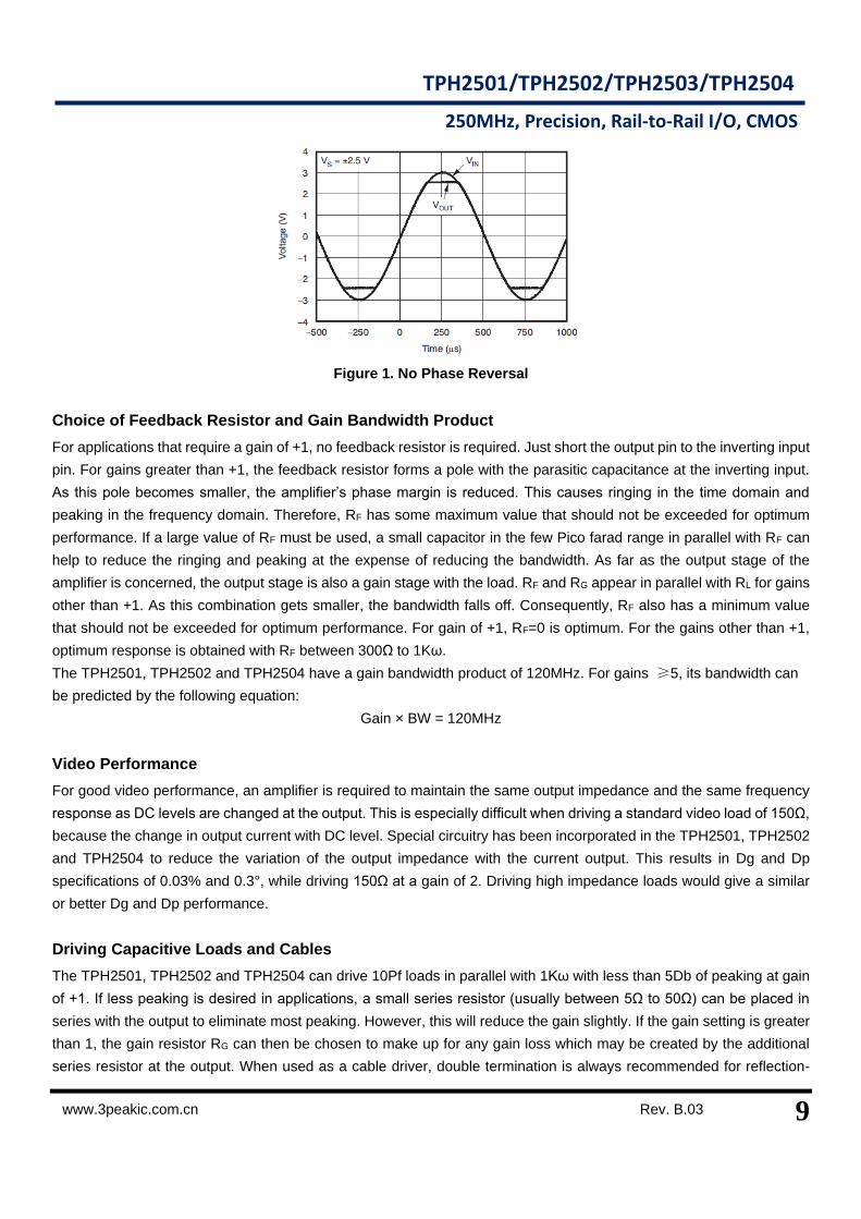
Rail-to-Rail Inputs and Outputs
The TPH2501,TPH2502,TPH2504 op amps are designed to be immune to phase reversal when the input pins exceed
the supply voltages, therefore providing further in-system stability and predictability. Figure 1 shows the input voltage
exceeding the supply voltage without any phase reversal.
9
TPH2501/TPH2502/TPH2503/TPH2504
250MHz, Precision, Rail-to-Rail I/O, CMOS
Op-amps
www.3peakic.com.cn Rev. B.03
Figure 1. No Phase Reversal
Choice of Feedback Resistor and Gain Bandwidth Product
For applications that require a gain of +1, no feedback resistor is required. Just short the output pin to the inverting input
pin. For gains greater than +1, the feedback resistor forms a pole with the parasitic capacitance at the inverting input.
As this pole becomes smaller, the amplifier’s phase margin is reduced. This causes ringing in the time domain and
peaking in the frequency domain. Therefore, RF has some maximum value that should not be exceeded for optimum
performance. If a large value of RF must be used, a small capacitor in the few Pico farad range in parallel with RF can
help to reduce the ringing and peaking at the expense of reducing the bandwidth. As far as the output stage of the
amplifier is concerned, the output stage is also a gain stage with the load. RF and RG appear in parallel with RL for gains
other than +1. As this combination gets smaller, the bandwidth falls off. Consequently, RF also has a minimum value
that should not be exceeded for optimum performance. For gain of +1, RF=0 is optimum. For the gains other than +1,
optimum response is obtained with RF between 300Ω to 1Kω.
The TPH2501, TPH2502 and TPH2504 have a gain bandwidth product of 120MHz. For gains ≥5, its bandwidth can
be predicted by the following equation:
Gain × BW = 120MHz
Video Performance
For good video performance, an amplifier is required to maintain the same output impedance and the same frequency
response as DC levels are changed at the output. This is especially difficult when driving a standard video load of 150Ω,
because the change in output current with DC level. Special circuitry has been incorporated in the TPH2501, TPH2502
and TPH2504 to reduce the variation of the output impedance with the current output. This results in Dg and Dp
specifications of 0.03% and 0.3°, while driving 150Ω at a gain of 2. Driving high impedance loads would give a similar
or better Dg and Dp performance.
Driving Capacitive Loads and Cables
The TPH2501, TPH2502 and TPH2504 can drive 10Pf loads in parallel with 1Kω with less than 5Db of peaking at gain
of +1. If less peaking is desired in applications, a small series resistor (usually between 5Ω to 50Ω) can be placed in
series with the output to eliminate most peaking. However, this will reduce the gain slightly. If the gain setting is greater
than 1, the gain resistor RG can then be chosen to make up for any gain loss which may be created by the additional
series resistor at the output. When used as a cable driver, double termination is always recommended for reflection-
10 Rev. B.03 www.3peakic.com.cn
TPH2501/TPH2502/TPH2503/TPH2504
250MHz, Precision, Rail-to-Rail I/O, CMOS Op-amps
free performance. For those applications, a back-termination series resistor at the amplifier’s output will isolate the
amplifier from the cable and allow extensive capacitive drive. However, other applications may have high capacitive
loads without a back-termination resistor. Again, a small series resistor at the output can help to reduce peaking.
Output Drive Capability
The TPH2501,TPH2502 and TPH2504 output stage can supply a continuous output current of ±100Ma and still provide
approximately 2.7V of output swing on a 5V supply. For maximum reliability, it is not recommended to run a continuous
DC current in excess of ±100Ma. Refer to the typical characteristic curve Output Voltage Swing vs Output Current. For
supplying continuous output currents greater than ±100Ma, the TPH250x may be operated in parallel. The TPH250x
will provide peak currents up to 200Ma, which corresponds to the typical short-circuit current. Therefore, an on-chip
thermal shutdown circuit is provided to protect the TPH250x from dangerously high junction temperatures. At 160°C,
the protection circuit will shut down the amplifier. Normal operation will resume when the junction temperature cools to
below 140°C.
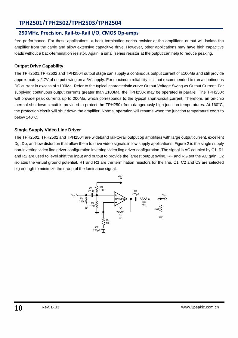
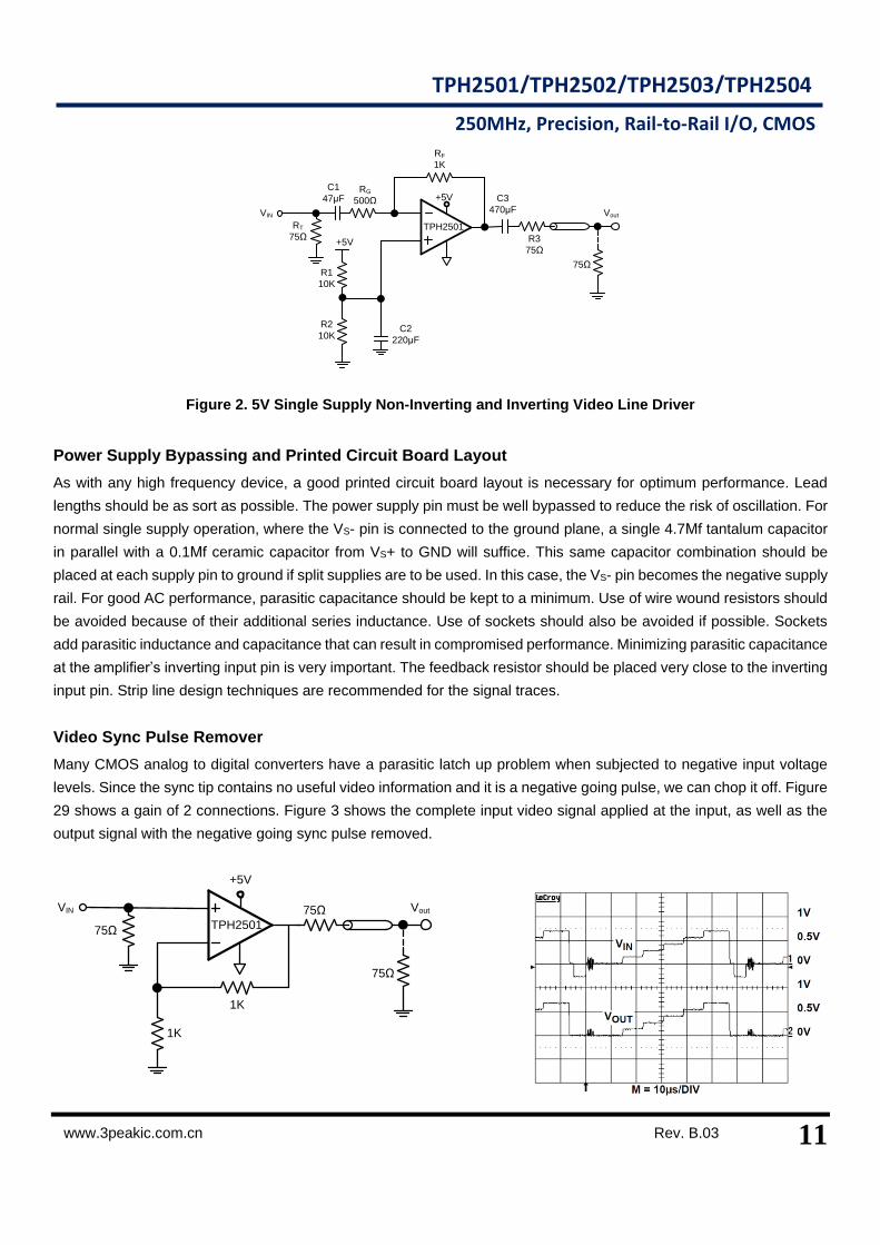
Single Supply Video Line Driver
The TPH2501, TPH2502 and TPH2504 are wideband rail-to-rail output op amplifiers with large output current, excellent
Dg, Dp, and low distortion that allow them to drive video signals in low supply applications. Figure 2 is the single supply
non-inverting video line driver configuration inverting video ling driver configuration. The signal is AC coupled by C1. R1
and R2 are used to level shift the input and output to provide the largest output swing. RF and RG set the AC gain. C2
isolates the virtual ground potential. RT and R3 are the termination resistors for the line. C1, C2 and C3 are selected
big enough to minimize the droop of the luminance signal.
VIN
TPH2501
Vout
+5V
RT
75Ω R3
75Ω
75Ω
RF
1K
R1
10K
R2
10K
C1
47μF
C2
220μF
C2
470μF
RG
1K
11
TPH2501/TPH2502/TPH2503/TPH2504
250MHz, Precision, Rail-to-Rail I/O, CMOS
Op-amps
www.3peakic.com.cn Rev. B.03
VIN
TPH2501
Vout
+5V
RT
75Ω R3
75Ω
75Ω
RF
1K
RG
500Ω
R2
10K
C1
47μF
C2
220μF
C3
470μF
R1
10K
+5V
Figure 2. 5V Single Supply Non-Inverting and Inverting Video Line Driver
Power Supply Bypassing and Printed Circuit Board Layout
As with any high frequency device, a good printed circuit board layout is necessary for optimum performance. Lead
lengths should be as sort as possible. The power supply pin must be well bypassed to reduce the risk of oscillation. For
normal single supply operation, where the VS- pin is connected to the ground plane, a single 4.7Μf tantalum capacitor
in parallel with a 0.1Μf ceramic capacitor from VS+ to GND will suffice. This same capacitor combination should be
placed at each supply pin to ground if split supplies are to be used. In this case, the VS- pin becomes the negative supply
rail. For good AC performance, parasitic capacitance should be kept to a minimum. Use of wire wound resistors should
be avoided because of their additional series inductance. Use of sockets should also be avoided if possible. Sockets
add parasitic inductance and capacitance that can result in compromised performance. Minimizing parasitic capacitance
at the amplifier’s inverting input pin is very important. The feedback resistor should be placed very close to the inverting
input pin. Strip line design techniques are recommended for the signal traces.
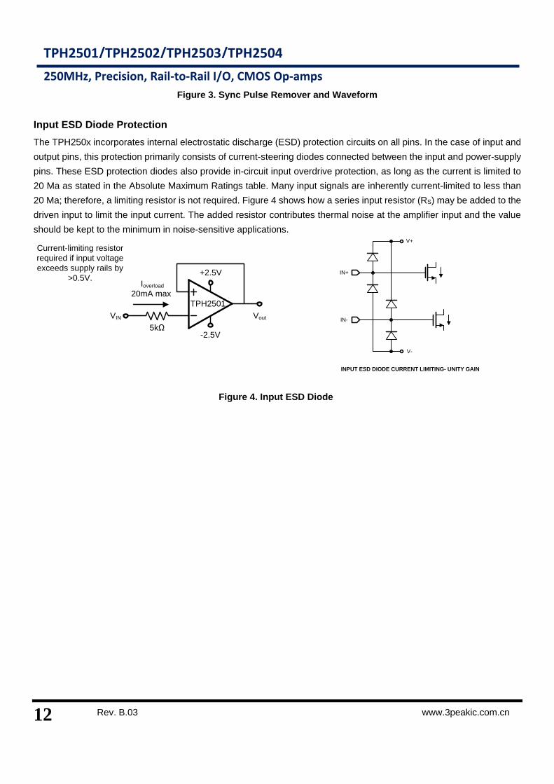
Video Sync Pulse Remover
Many CMOS analog to digital converters have a parasitic latch up problem when subjected to negative input voltage
levels. Since the sync tip contains no useful video information and it is a negative going pulse, we can chop it off. Figure
29 shows a gain of 2 connections. Figure 3 shows the complete input video signal applied at the input, as well as the
output signal with the negative going sync pulse removed.
VIN
TPH2501
Vout
+5V
75Ω
75Ω
75Ω
1K
1K
12 Rev. B.03 www.3peakic.com.cn
TPH2501/TPH2502/TPH2503/TPH2504
250MHz, Precision, Rail-to-Rail I/O, CMOS Op-amps
Figure 3. Sync Pulse Remover and Waveform
Input ESD Diode Protection
The TPH250x incorporates internal electrostatic discharge (ESD) protection circuits on all pins. In the case of input and
output pins, this protection primarily consists of current-steering diodes connected between the input and power-supply
pins. These ESD protection diodes also provide in-circuit input overdrive protection, as long as the current is limited to
20 Ma as stated in the Absolute Maximum Ratings table. Many input signals are inherently current-limited to less than
20 Ma; therefore, a limiting resistor is not required. Figure 4 shows how a series input resistor (RS) may be added to the
driven input to limit the input current. The added resistor contributes thermal noise at the amplifier input and the value
should be kept to the minimum in noise-sensitive applications.
IN+
IN-
V+
V-
INPUT ESD DIODE CURRENT LIMITING- UNITY GAIN
Figure 4. Input ESD Diode
Ioverload
20mA max
VIN
Current-limiting resistor
required if input voltage
exceeds supply rails by
>0.5V.
TPH2501
Vout
+2.5V
-2.5V5kΩ
13
TPH2501/TPH2502/TPH2503/TPH2504
250MHz, Precision, Rail-to-Rail I/O, CMOS
Op-amps
www.3peakic.com.cn Rev. B.03
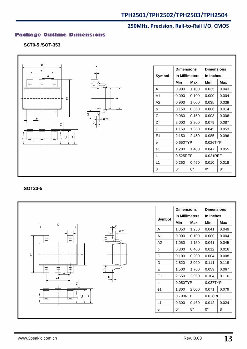
Package Outline Dimensions
SC70-5 /SOT-353
SOT23-5
Symbol
Dimensions
In Millimeters
Dimensions
In Inches
Min Max Min Max
A 1.050 1.250 0.041 0.049
A1 0.000 0.100 0.000 0.004
A2 1.050 1.150 0.041 0.045
b 0.300 0.400 0.012 0.016
C 0.100 0.200 0.004 0.008
D 2.820 3.020 0.111 0.119
E 1.500 1.700 0.059 0.067
E1 2.650 2.950 0.104 0.116
e 0.950TYP 0.037TYP
e1 1.800 2.000 0.071 0.079
L 0.700REF 0.028REF
L1 0.300 0.460 0.012 0.024
θ 0° 8° 0° 8°
Symbol
Dimensions
In Millimeters
Dimensions
In Inches
Min Max Min Max
A 0.900 1.100 0.035 0.043
A1 0.000 0.100 0.000 0.004
A2 0.900 1.000 0.035 0.039
b 0.150 0.350 0.006 0.014
C 0.080 0.150 0.003 0.006
D 2.000 2.200 0.079 0.087
E 1.150 1.350 0.045 0.053
E1 2.150 2.450 0.085 0.096
e 0.650TYP 0.026TYP
e1 1.200 1.400 0.047 0.055
L 0.525REF 0.021REF
L1 0.260 0.460 0.010 0.018
θ 0° 8° 0° 8°
14 Rev. B.03 www.3peakic.com.cn
TPH2501/TPH2502/TPH2503/TPH2504
250MHz, Precision, Rail-to-Rail I/O, CMOS Op-amps
D
e
A2
A1
E
E1
e1
b
L1θ
Package Outline Dimensions
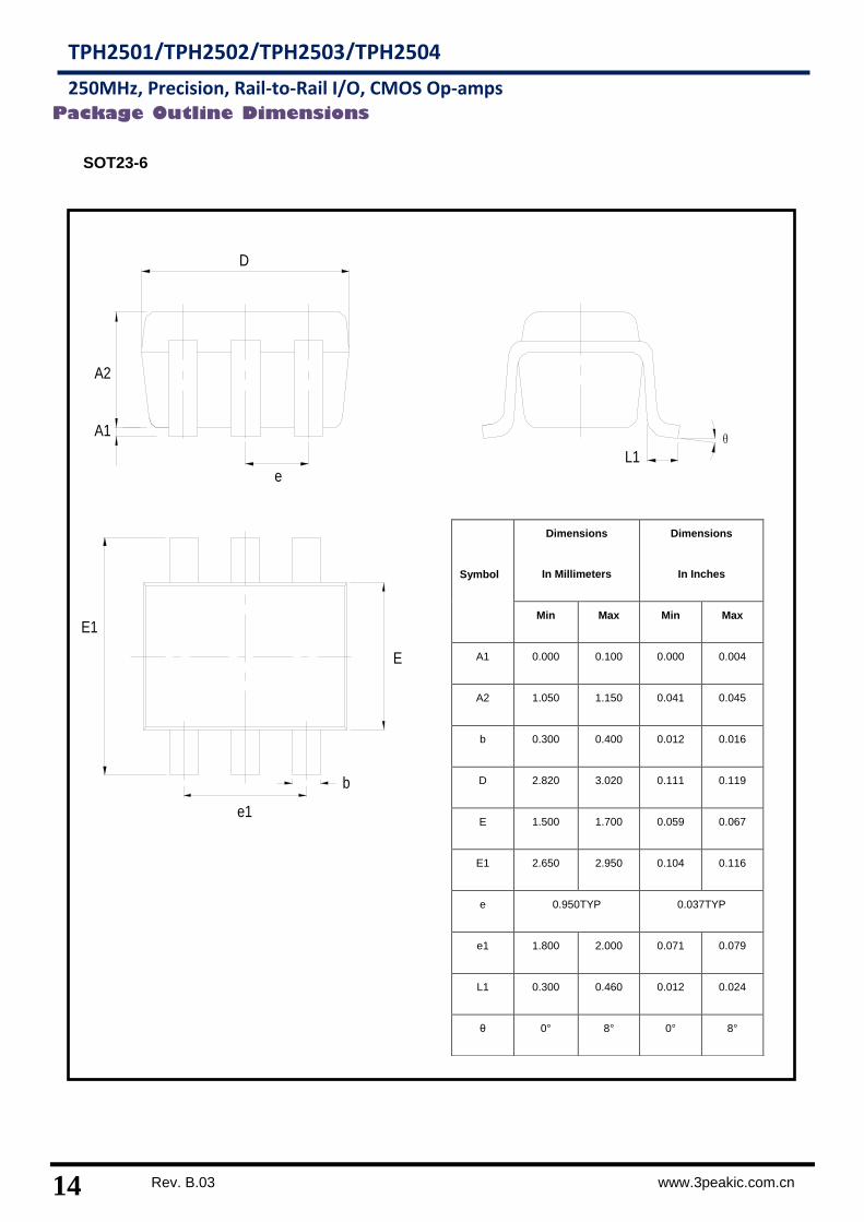
SOT23-6
Symbol
Dimensions
In Millimeters
Dimensions
In Inches
Min Max Min Max
A1 0.000 0.100 0.000 0.004
A2 1.050 1.150 0.041 0.045
b 0.300 0.400 0.012 0.016
D 2.820 3.020 0.111 0.119
E 1.500 1.700 0.059 0.067
E1 2.650 2.950 0.104 0.116
e 0.950TYP 0.037TYP
e1 1.800 2.000 0.071 0.079
L1 0.300 0.460 0.012 0.024
θ 0° 8° 0° 8°
15
TPH2501/TPH2502/TPH2503/TPH2504
250MHz, Precision, Rail-to-Rail I/O, CMOS
Op-amps
www.3peakic.com.cn Rev. B.03
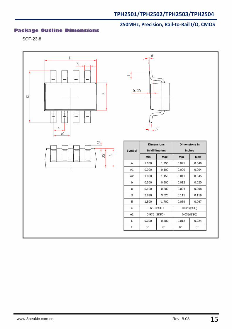
Package Outline Dimensions
SOT-23-8
Symbol
Dimensions
In Millimeters
Dimensions In
Inches
Min Max Min Max
A 1.050 1.250 0.041 0.049
A1 0.000 0.100 0.000 0.004
A2 1.050 1.150 0.041 0.045
b 0.300 0.500 0.012 0.020
c 0.100 0.200 0.004 0.008
D 2.820 3.020 0.111 0.119
E 1.500 1.700 0.059 0.067
e 0.65(BSC) 0.026(BSC)
e1 0.975(BSC) 0.038(BSC)
L 0.300 0.600 0.012 0.024
θ 0° 8° 0° 8°
16 Rev. B.03 www.3peakic.com.cn
TPH2501/TPH2502/TPH2503/TPH2504
250MHz, Precision, Rail-to-Rail I/O, CMOS Op-amps
D
E1
b
E
A1
A2
e
θ
L1
C
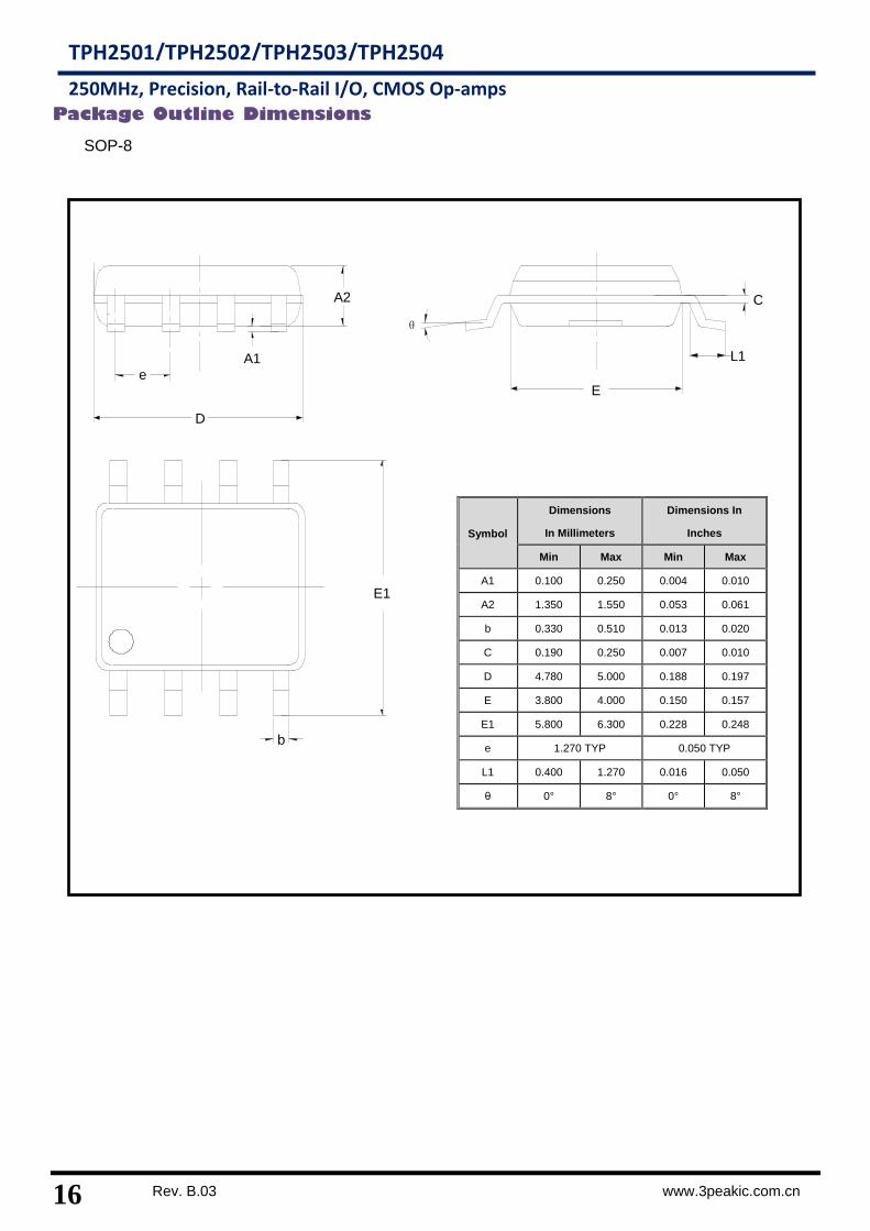
Package Outline Dimensions
SOP-8
Symbol
Dimensions
In Millimeters
Dimensions In
Inches
Min Max Min Max
A1 0.100 0.250 0.004 0.010
A2 1.350 1.550 0.053 0.061
b 0.330 0.510 0.013 0.020
C 0.190 0.250 0.007 0.010
D 4.780 5.000 0.188 0.197
E 3.800 4.000 0.150 0.157
E1 5.800 6.300 0.228 0.248
e 1.270 TYP 0.050 TYP
L1 0.400 1.270 0.016 0.050
θ 0° 8° 0° 8°
17
TPH2501/TPH2502/TPH2503/TPH2504
250MHz, Precision, Rail-to-Rail I/O, CMOS
Op-amps
www.3peakic.com.cn Rev. B.03
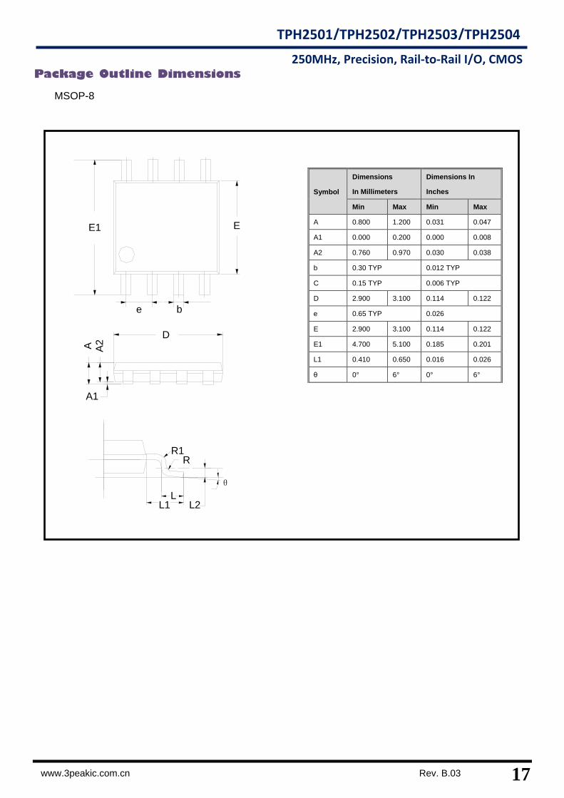
Package Outline Dimensions
MSOP-8
Symbol
Dimensions
In Millimeters
Dimensions In
Inches
Min Max Min Max
A 0.800 1.200 0.031 0.047
A1 0.000 0.200 0.000 0.008
A2 0.760 0.970 0.030 0.038
b 0.30 TYP 0.012 TYP
C 0.15 TYP 0.006 TYP
D 2.900 3.100 0.114 0.122
e 0.65 TYP 0.026
E 2.900 3.100 0.114 0.122
E1 4.700 5.100 0.185 0.201
L1 0.410 0.650 0.016 0.026
θ 0° 6° 0° 6°
E1
e
E
A1
A2A
D
L1 L2L
RR1
θ
b
18 Rev. B.03 www.3peakic.com.cn
TPH2501/TPH2502/TPH2503/TPH2504
250MHz, Precision, Rail-to-Rail I/O, CMOS Op-amps
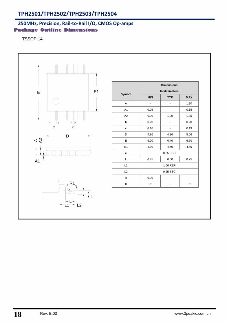
Package Outline Dimensions
TSSOP-14
Symbol
Dimensions
In Millimeters
MIN TYP MAX
A - - 1.20
A1 0.05 - 0.15
A2 0.90 1.00 1.05
b 0.20 - 0.28
c 0.10 - 0.19
D 4.86 4.96 5.06
E 6.20 6.40 6.60
E1 4.30 4.40 4.50
e 0.65 BSC
L 0.45 0.60 0.75
L1 1.00 REF
L2 0.25 BSC
R 0.09 - -
θ 0° - 8°
E
e
E1
A1
A2A
D
L1 L2L
RR1
θ
c
19
TPH2501/TPH2502/TPH2503/TPH2504
250MHz, Precision, Rail-to-Rail I/O, CMOS
Op-amps
www.3peakic.com.cn Rev. B.03
θ
e b
E1 E
D
A1
A A2
L1L
L2
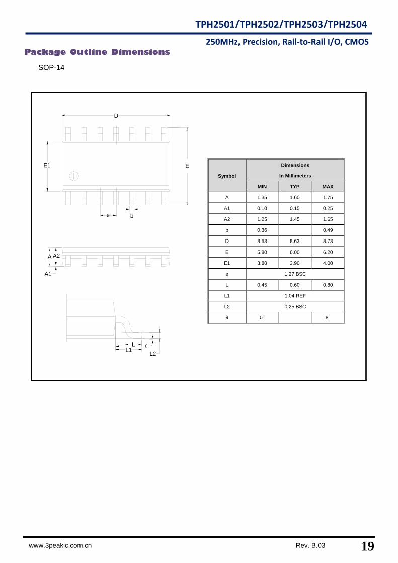
Package Outline Dimensions
SOP-14
Symbol
Dimensions
In Millimeters
MIN TYP MAX
A 1.35 1.60 1.75
A1 0.10 0.15 0.25
A2 1.25 1.45 1.65
b 0.36 0.49
D 8.53 8.63 8.73
E 5.80 6.00 6.20
E1 3.80 3.90 4.00
e 1.27 BSC
L 0.45 0.60 0.80
L1 1.04 REF
L2 0.25 BSC
θ 0° 8°
20 Rev. B.03 www.3peakic.com.cn
TPH2501/TPH2502/TPH2503/TPH2504
250MHz, Precision, Rail-to-Rail I/O, CMOS Op-amps
Revision History
2018/8/20 Rev B Update Full Temperature Specification
2018/12/25 Rev B01 Correct Mark of TPH2501L1-TR: “501”->“50L”.
Add Power On Requirement in Application Information.
2019/11/14 Rev B02 Correct the typo error in Input Bias Current Vs. Temperature: Unit “pA”
-> “nA”; Add input logic voltage of shut down.
2019/12/16 Rev B03 Correct the typo error in TPH2503 pin configuration on page1.