Low voltage brush DC motor driver - STMicroelectronics · Low voltage brush DC motor driver...
26
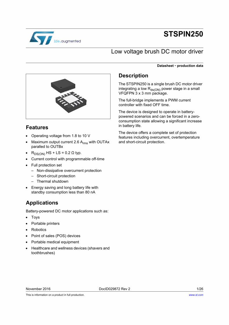
This is information on a product in full production. November 2016 DocID029872 Rev 2 1/26 STSPIN250 Low voltage brush DC motor driver Datasheet - production data Features Operating voltage from 1.8 to 10 V Maximum output current 2.6 A rms with OUTAx paralled to OUTBx R DS(ON) HS + LS = 0.2 Ω typ. Current control with programmable off-time Full protection set – Non-dissipative overcurrent protection – Short-circuit protection – Thermal shutdown Energy saving and long battery life with standby consumption less than 80 nA Applications Battery-powered DC motor applications such as: Toys Portable printers Robotics Point of sales (POS) devices Portable medical equipment Healthcare and wellness devices (shavers and toothbrushes) Description The STSPIN250 is a single brush DC motor driver integrating a low R ds(ON) power stage in a small VFQFPN 3 x 3 mm package. The full-bridge implements a PWM current controller with fixed OFF time. The device is designed to operate in battery- powered scenarios and can be forced in a zero- consumption state allowing a significant increase in battery life. The device offers a complete set of protection features including overcurrent, overtemperature and short-circuit protection. www.st.com
Transcript of Low voltage brush DC motor driver - STMicroelectronics · Low voltage brush DC motor driver...
This is information on a product in full production.
November 2016 DocID029872 Rev 2 1/26
STSPIN250
Low voltage brush DC motor driver
Datasheet - production data
Features
Operating voltage from 1.8 to 10 V
Maximum output current 2.6 Arms with OUTAx paralled to OUTBx
RDS(ON) HS + LS = 0.2 Ω typ.
Current control with programmable off-time
Full protection set
– Non-dissipative overcurrent protection
– Short-circuit protection
– Thermal shutdown
Energy saving and long battery life with standby consumption less than 80 nA
Applications
Battery-powered DC motor applications such as:
Toys
Portable printers
Robotics
Point of sales (POS) devices
Portable medical equipment
Healthcare and wellness devices (shavers and toothbrushes)
Description
The STSPIN250 is a single brush DC motor driver integrating a low Rds(ON) power stage in a small VFQFPN 3 x 3 mm package.
The full-bridge implements a PWM current controller with fixed OFF time.
The device is designed to operate in battery-powered scenarios and can be forced in a zero-consumption state allowing a significant increase in battery life.
The device offers a complete set of protection features including overcurrent, overtemperature and short-circuit protection.
www.st.com
Contents STSPIN250
2/26 DocID029872 Rev 2
Contents
1 Block diagram . . . . . . . . . . . . . . . . . . . . . . . . . . . . . . . . . . . . . . . . . . . . . . 5
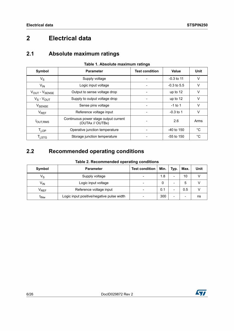
2 Electrical data . . . . . . . . . . . . . . . . . . . . . . . . . . . . . . . . . . . . . . . . . . . . . . 6
2.1 Absolute maximum ratings . . . . . . . . . . . . . . . . . . . . . . . . . . . . . . . . . . . . . 6
2.2 Recommended operating conditions . . . . . . . . . . . . . . . . . . . . . . . . . . . . . 6
2.3 Thermal data . . . . . . . . . . . . . . . . . . . . . . . . . . . . . . . . . . . . . . . . . . . . . . . 7
2.4 ESD protections . . . . . . . . . . . . . . . . . . . . . . . . . . . . . . . . . . . . . . . . . . . . . 7
3 Electrical characteristics . . . . . . . . . . . . . . . . . . . . . . . . . . . . . . . . . . . . . 8
4 Pin description . . . . . . . . . . . . . . . . . . . . . . . . . . . . . . . . . . . . . . . . . . . . 10
5 Typical applications . . . . . . . . . . . . . . . . . . . . . . . . . . . . . . . . . . . . . . . . 12
6 Device description . . . . . . . . . . . . . . . . . . . . . . . . . . . . . . . . . . . . . . . . . 13
6.1 Standby and power-up . . . . . . . . . . . . . . . . . . . . . . . . . . . . . . . . . . . . . . . 13
6.2 Motor driving . . . . . . . . . . . . . . . . . . . . . . . . . . . . . . . . . . . . . . . . . . . . . . . 13
6.3 PWM current control . . . . . . . . . . . . . . . . . . . . . . . . . . . . . . . . . . . . . . . . . 15
TOFF adjustment . . . . . . . . . . . . . . . . . . . . . . . . . . . . . . . . . . . . . . . . . . . . . . . . . . 17
6.4 Overcurrent and short-circuit protections . . . . . . . . . . . . . . . . . . . . . . . . . 18
6.5 Thermal shutdown . . . . . . . . . . . . . . . . . . . . . . . . . . . . . . . . . . . . . . . . . . 20
7 Graphs . . . . . . . . . . . . . . . . . . . . . . . . . . . . . . . . . . . . . . . . . . . . . . . . . . . 21
8 Package information . . . . . . . . . . . . . . . . . . . . . . . . . . . . . . . . . . . . . . . . 23
8.1 VFQFPN 3 x 3 x 1.0- 16L package information . . . . . . . . . . . . . . . . . . . . 23
9 Ordering information . . . . . . . . . . . . . . . . . . . . . . . . . . . . . . . . . . . . . . . 25
10 Revision history . . . . . . . . . . . . . . . . . . . . . . . . . . . . . . . . . . . . . . . . . . . 25
DocID029872 Rev 2 3/26
STSPIN250 List of tables
26
List of tables
Table 1. Absolute maximum ratings . . . . . . . . . . . . . . . . . . . . . . . . . . . . . . . . . . . . . . . . . . . . . . . . . . 6Table 2. Recommended operating conditions . . . . . . . . . . . . . . . . . . . . . . . . . . . . . . . . . . . . . . . . . . 6Table 3. Thermal data. . . . . . . . . . . . . . . . . . . . . . . . . . . . . . . . . . . . . . . . . . . . . . . . . . . . . . . . . . . . . 7Table 4. ESD protection ratings . . . . . . . . . . . . . . . . . . . . . . . . . . . . . . . . . . . . . . . . . . . . . . . . . . . . . 7Table 5. Electrical characteristics . . . . . . . . . . . . . . . . . . . . . . . . . . . . . . . . . . . . . . . . . . . . . . . . . . . . 8Table 6. Pin description . . . . . . . . . . . . . . . . . . . . . . . . . . . . . . . . . . . . . . . . . . . . . . . . . . . . . . . . . . 10Table 7. Typical application values. . . . . . . . . . . . . . . . . . . . . . . . . . . . . . . . . . . . . . . . . . . . . . . . . . 12Table 8. Truth table. . . . . . . . . . . . . . . . . . . . . . . . . . . . . . . . . . . . . . . . . . . . . . . . . . . . . . . . . . . . . . 13Table 9. ON and slow decay states . . . . . . . . . . . . . . . . . . . . . . . . . . . . . . . . . . . . . . . . . . . . . . . . . 15Table 10. Recommended RRCOFF and CRCOFF values according to ROFF . . . . . . . . . . . . . . . . . . . . 17Table 11. VFQFPN 3 x 3 x 1.0 - 16L package mechanical data. . . . . . . . . . . . . . . . . . . . . . . . . . . . . 24Table 12. Device summary . . . . . . . . . . . . . . . . . . . . . . . . . . . . . . . . . . . . . . . . . . . . . . . . . . . . . . . . . 25Table 13. Document revision history . . . . . . . . . . . . . . . . . . . . . . . . . . . . . . . . . . . . . . . . . . . . . . . . . 25
List of figures STSPIN250
4/26 DocID029872 Rev 2
List of figures
Figure 1. Block diagram . . . . . . . . . . . . . . . . . . . . . . . . . . . . . . . . . . . . . . . . . . . . . . . . . . . . . . . . . . . . 5Figure 2. Pin connection (top view) . . . . . . . . . . . . . . . . . . . . . . . . . . . . . . . . . . . . . . . . . . . . . . . . . . 10Figure 3. Typical application schematic . . . . . . . . . . . . . . . . . . . . . . . . . . . . . . . . . . . . . . . . . . . . . . . 12Figure 4. Timing diagram . . . . . . . . . . . . . . . . . . . . . . . . . . . . . . . . . . . . . . . . . . . . . . . . . . . . . . . . . . 14Figure 5. PWM current control . . . . . . . . . . . . . . . . . . . . . . . . . . . . . . . . . . . . . . . . . . . . . . . . . . . . . . 16Figure 6. OFF time regulation circuit . . . . . . . . . . . . . . . . . . . . . . . . . . . . . . . . . . . . . . . . . . . . . . . . . 17Figure 7. OFF time vs ROFF value . . . . . . . . . . . . . . . . . . . . . . . . . . . . . . . . . . . . . . . . . . . . . . . . . . . 17Figure 8. Overcurrent and short-circuit protections management . . . . . . . . . . . . . . . . . . . . . . . . . . . 18Figure 9. Disable time versus REN and CEN values (VDD = 3.3 V) . . . . . . . . . . . . . . . . . . . . . . . . . . 19Figure 10. Disable time versus REN and CEN values (VDD = 1.8 V) . . . . . . . . . . . . . . . . . . . . . . . . . . 19Figure 11. Thermal shutdown management . . . . . . . . . . . . . . . . . . . . . . . . . . . . . . . . . . . . . . . . . . . . 20Figure 12. Power stage resistance versus supply voltage . . . . . . . . . . . . . . . . . . . . . . . . . . . . . . . . . 21Figure 13. Power stage resistance versus temperature . . . . . . . . . . . . . . . . . . . . . . . . . . . . . . . . . . . 21Figure 14. Overcurrent threshold versus supply voltage . . . . . . . . . . . . . . . . . . . . . . . . . . . . . . . . . . . 22Figure 15. VFQFPN 3 x 3 x 1.0 - 16L package outline . . . . . . . . . . . . . . . . . . . . . . . . . . . . . . . . . . . . 23Figure 16. VFQFPN 3 x 3 x 1.0 - 16L recommended footprint . . . . . . . . . . . . . . . . . . . . . . . . . . . . . . 24
DocID029872 Rev 2 5/26
STSPIN250 Block diagram
26
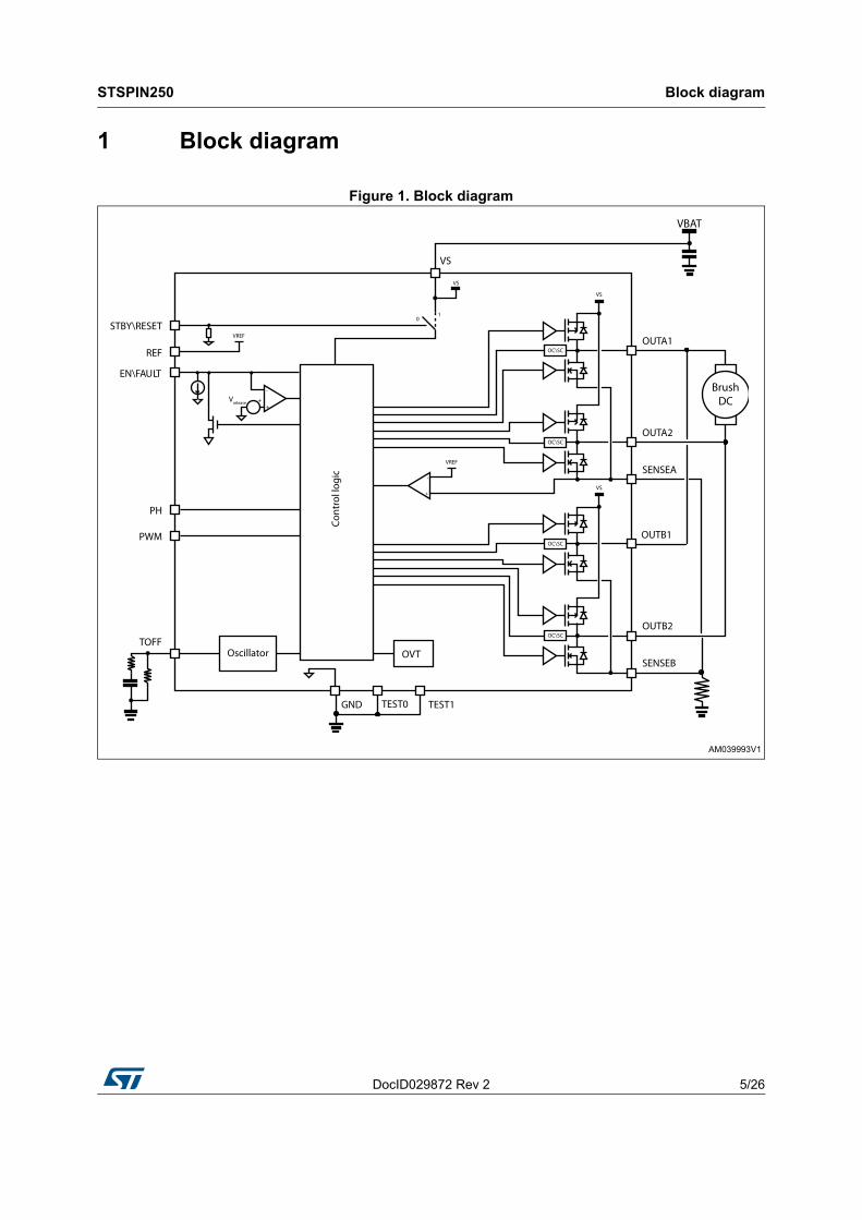
1 Block diagram
Figure 1. Block diagram
Electrical data STSPIN250
6/26 DocID029872 Rev 2
2 Electrical data
2.1 Absolute maximum ratings
2.2 Recommended operating conditions
Table 1. Absolute maximum ratings
Symbol Parameter Test condition Value Unit
VS Supply voltage - -0.3 to 11 V
VIN Logic input voltage - -0.3 to 5.5 V
VOUT - VSENSE Output to sense voltage drop - up to 12 V
VS - VOUT Supply to output voltage drop - up to 12 V
VSENSE Sense pins voltage - -1 to 1 V
VREF Reference voltage input - -0.3 to 1 V
IOUT,RMSContinuous power stage output current
(OUTAx // OUTBx)- 2.6 Arms
Tj,OP Operative junction temperature - -40 to 150 °C
Tj,STG Storage junction temperature - -55 to 150 °C
Table 2. Recommended operating conditions
Symbol Parameter Test condition Min. Typ. Max. Unit
VS Supply voltage - 1.8 - 10 V
VIN Logic input voltage - 0 - 5 V
VREF Reference voltage input - 0.1 - 0.5 V
tINw Logic input positive/negative pulse width - 300 - - ns
DocID029872 Rev 2 7/26
STSPIN250 Electrical data
26
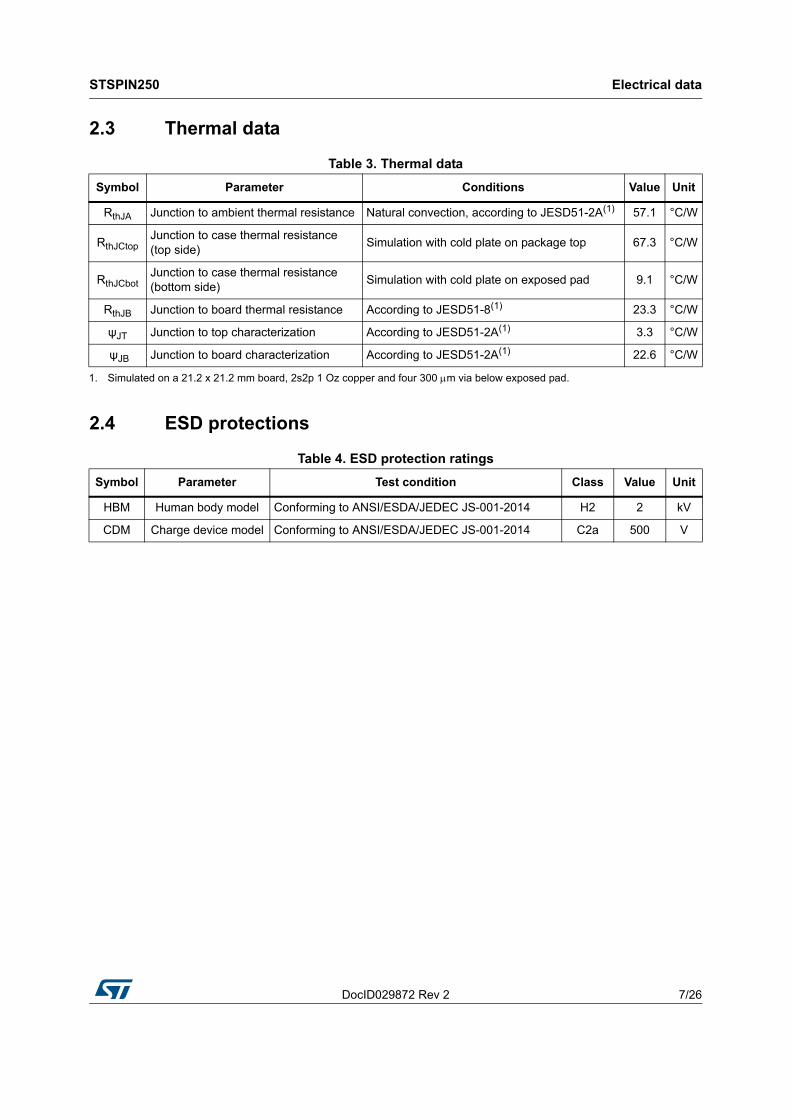
2.3 Thermal data
2.4 ESD protections
Table 3. Thermal data
Symbol Parameter Conditions Value Unit
RthJA Junction to ambient thermal resistance Natural convection, according to JESD51-2A(1) 57.1 °C/W
RthJCtopJunction to case thermal resistance (top side)
Simulation with cold plate on package top 67.3 °C/W
RthJCbotJunction to case thermal resistance (bottom side)
Simulation with cold plate on exposed pad 9.1 °C/W
RthJB Junction to board thermal resistance According to JESD51-8(1) 23.3 °C/W
ψJT Junction to top characterization According to JESD51-2A(1) 3.3 °C/W
ψJB Junction to board characterization According to JESD51-2A(1) 22.6 °C/W
1. Simulated on a 21.2 x 21.2 mm board, 2s2p 1 Oz copper and four 300 m via below exposed pad.
Table 4. ESD protection ratings
Symbol Parameter Test condition Class Value Unit
HBM Human body model Conforming to ANSI/ESDA/JEDEC JS-001-2014 H2 2 kV
CDM Charge device model Conforming to ANSI/ESDA/JEDEC JS-001-2014 C2a 500 V
Electrical characteristics STSPIN250
8/26 DocID029872 Rev 2
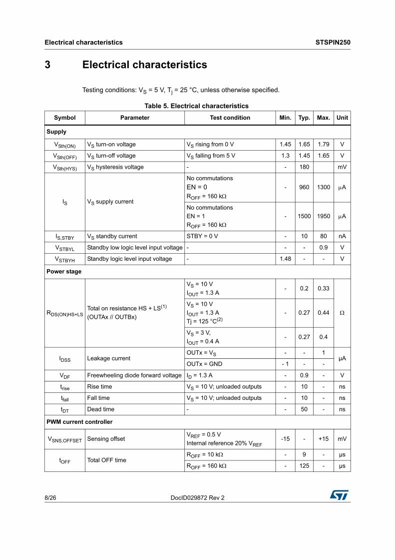
3 Electrical characteristics
Testing conditions: VS = 5 V, Tj = 25 °C, unless otherwise specified.
Table 5. Electrical characteristics
Symbol Parameter Test condition Min. Typ. Max. Unit
Supply
VSth(ON) VS turn-on voltage VS rising from 0 V 1.45 1.65 1.79 V
VSth(OFF) VS turn-off voltage VS falling from 5 V 1.3 1.45 1.65 V
VSth(HYS) VS hysteresis voltage - - 180 mV
IS VS supply current
No commutations
EN = 0ROFF = 160 k
- 960 1300 A
No commutations
EN = 1
ROFF = 160 k- 1500 1950 A
IS,STBY VS standby current STBY = 0 V - 10 80 nA
VSTBYL Standby low logic level input voltage - - - 0.9 V
VSTBYH Standby logic level input voltage - 1.48 - - V
Power stage
RDS(ON)HS+LSTotal on resistance HS + LS(1)
(OUTAx // OUTBx)
VS = 10 V
IOUT = 1.3 A- 0.2 0.33
VS = 10 V
IOUT = 1.3 A
Tj = 125 °C(2)- 0.27 0.44
VS = 3 V,
IOUT = 0.4 A- 0.27 0.4
IDSS Leakage currentOUTx = VS - - 1
µAOUTx = GND - 1 - -
VDF Freewheeling diode forward voltage ID = 1.3 A - 0.9 - V
trise Rise time VS = 10 V; unloaded outputs - 10 - ns
tfall Fall time VS = 10 V; unloaded outputs - 10 - ns
tDT Dead time - - 50 - ns
PWM current controller
VSNS,OFFSET Sensing offsetVREF = 0.5 V
Internal reference 20% VREF-15 - +15 mV
tOFF Total OFF timeROFF = 10 k - 9 - µs
ROFF = 160 k - 125 - µs
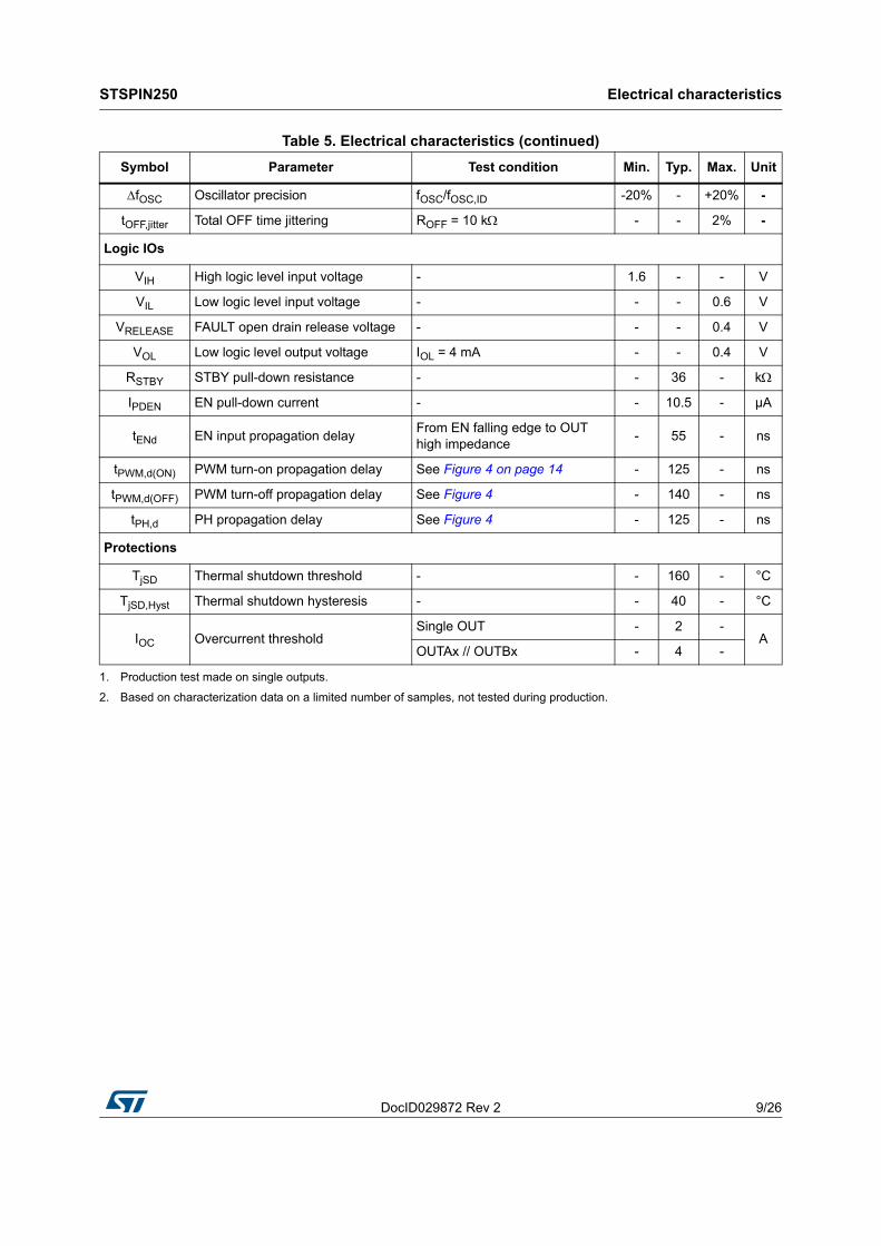
DocID029872 Rev 2 9/26
STSPIN250 Electrical characteristics
26
fOSC Oscillator precision fOSC/fOSC,ID -20% - +20% -
tOFF,jitter Total OFF time jittering ROFF = 10 k - - 2% -
Logic IOs
VIH High logic level input voltage - 1.6 - - V
VIL Low logic level input voltage - - - 0.6 V
VRELEASE FAULT open drain release voltage - - - 0.4 V
VOL Low logic level output voltage IOL = 4 mA - - 0.4 V
RSTBY STBY pull-down resistance - - 36 - k
IPDEN EN pull-down current - - 10.5 - µA
tENd EN input propagation delayFrom EN falling edge to OUT high impedance
- 55 - ns
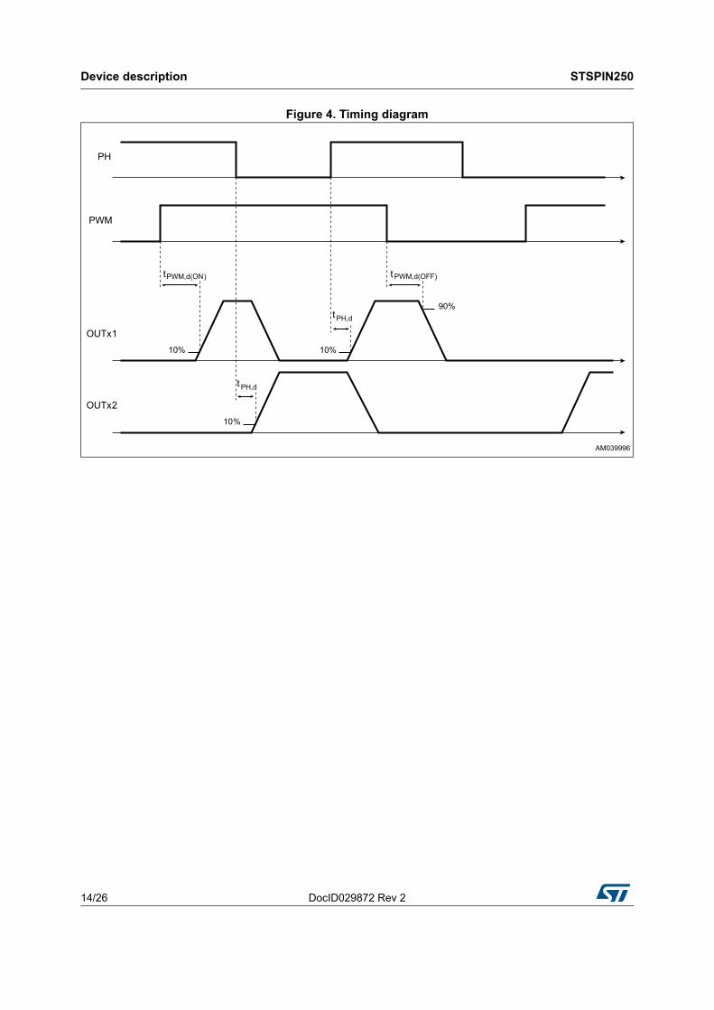
tPWM,d(ON) PWM turn-on propagation delay See Figure 4 on page 14 - 125 - ns
tPWM,d(OFF) PWM turn-off propagation delay See Figure 4 - 140 - ns
tPH,d PH propagation delay See Figure 4 - 125 - ns
Protections
TjSD Thermal shutdown threshold - - 160 - °C
TjSD,Hyst Thermal shutdown hysteresis - - 40 - °C
IOC Overcurrent thresholdSingle OUT - 2 -
AOUTAx // OUTBx - 4 -
1. Production test made on single outputs.
2. Based on characterization data on a limited number of samples, not tested during production.
Table 5. Electrical characteristics (continued)
Symbol Parameter Test condition Min. Typ. Max. Unit
Pin description STSPIN250
10/26 DocID029872 Rev 2
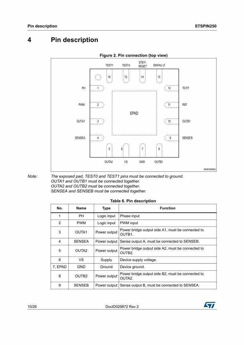
4 Pin description
Figure 2. Pin connection (top view)
Note: The exposed pad, TEST0 and TEST1 pins must be connected to ground.OUTA1 and OUTB1 must be connected together.OUTA2 and OUTB2 must be connected together.SENSEA and SENSEB must be connected together.
Table 6. Pin description
No. Name Type Function
1 PH Logic input Phase input
2 PWM Logic input PWM input
3 OUTA1 Power outputPower bridge output side A1, must be connected to OUTB1.
4 SENSEA Power output Sense output A, must be connected to SENSEB.
5 OUTA2 Power outputPower bridge output side A2, must be connected to OUTB2.
6 VS Supply Device supply voltage.
7, EPAD GND Ground Device ground.
8 OUTB2 Power outputPower bridge output side B2, must be connected to OUTA2.
9 SENSEB Power output Sense output B, must be connected to SENSEA.
DocID029872 Rev 2 11/26
STSPIN250 Pin description
26
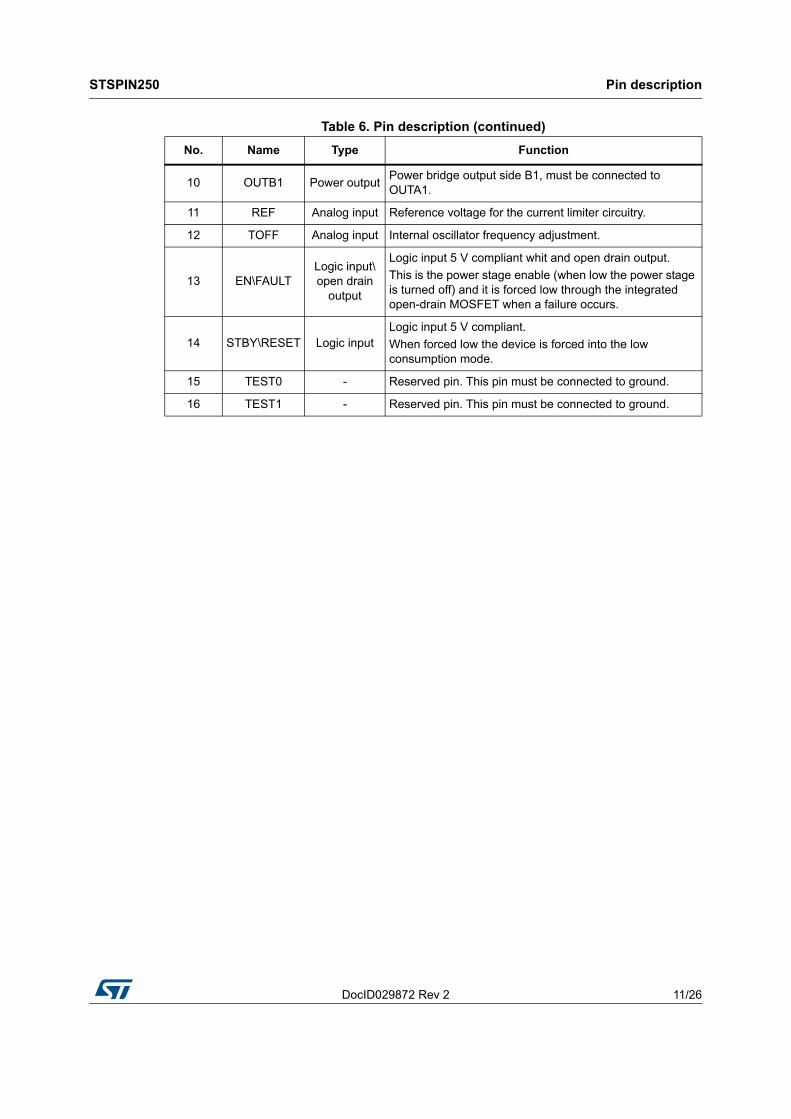
10 OUTB1 Power outputPower bridge output side B1, must be connected to OUTA1.
11 REF Analog input Reference voltage for the current limiter circuitry.
12 TOFF Analog input Internal oscillator frequency adjustment.
13 EN\FAULTLogic input\ open drain
output
Logic input 5 V compliant whit and open drain output.
This is the power stage enable (when low the power stage is turned off) and it is forced low through the integrated open-drain MOSFET when a failure occurs.
14 STBY\RESET Logic inputLogic input 5 V compliant.
When forced low the device is forced into the low consumption mode.
15 TEST0 - Reserved pin. This pin must be connected to ground.
16 TEST1 - Reserved pin. This pin must be connected to ground.
Table 6. Pin description (continued)
No. Name Type Function
Typical applications STSPIN250
12/26 DocID029872 Rev 2
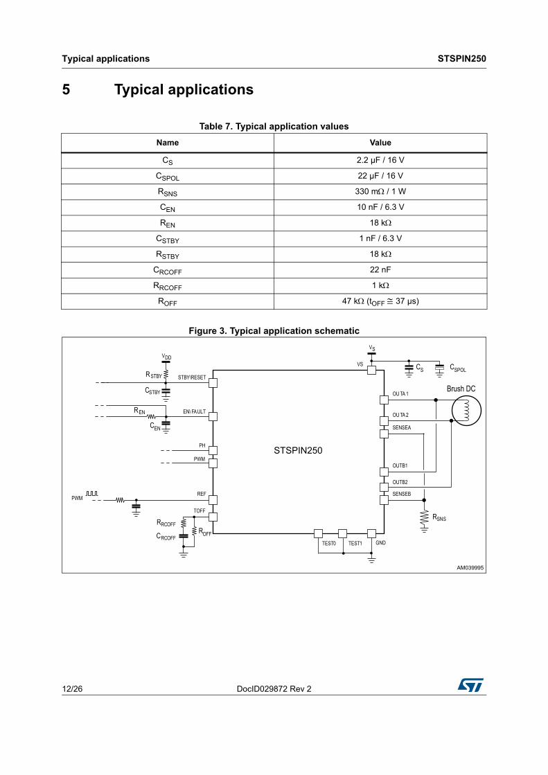
5 Typical applications
Figure 3. Typical application schematic
Table 7. Typical application values
Name Value
CS 2.2 µF / 16 V
CSPOL 22 µF / 16 V
RSNS 330 m / 1 W
CEN 10 nF / 6.3 V
REN 18 k
CSTBY 1 nF / 6.3 V
RSTBY 18 k
CRCOFF 22 nF
RRCOFF 1 k
ROFF 47 k (tOFF 37 µs)
DocID029872 Rev 2 13/26
STSPIN250 Device description
26
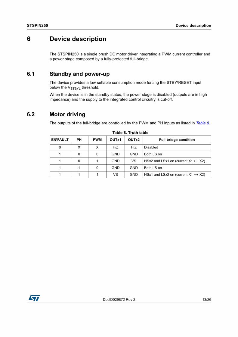
6 Device description
The STSPIN250 is a single brush DC motor driver integrating a PWM current controller and a power stage composed by a fully-protected full-bridge.
6.1 Standby and power-up
The device provides a low settable consumption mode forcing the STBY\RESET input below the VSTBYL threshold.
When the device is in the standby status, the power stage is disabled (outputs are in high impedance) and the supply to the integrated control circuitry is cut-off.
6.2 Motor driving
The outputs of the full-bridge are controlled by the PWM and PH inputs as listed in Table 8.
Table 8. Truth table
EN\FAULT PH PWM OUTx1 OUTx2 Full-bridge condition
0 X X HiZ HiZ Disabled
1 0 0 GND GND Both LS on
1 0 1 GND VS HSx2 and LSx1 on (current X1 X2)
1 1 0 GND GND Both LS on
1 1 1 VS GND HSx1 and LSx2 on (current X1 X2)
Device description STSPIN250
14/26 DocID029872 Rev 2
Figure 4. Timing diagram
DocID029872 Rev 2 15/26
STSPIN250 Device description
26
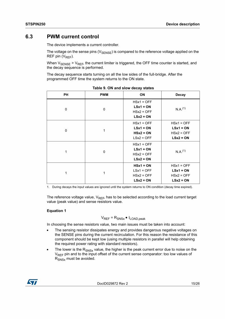
6.3 PWM current control
The device implements a current controller.
The voltage on the sense pins (VSENSE) is compared to the reference voltage applied on the REF pin (VREF).
When VSENSE > VREF, the current limiter is triggered, the OFF time counter is started, and the decay sequence is performed.
The decay sequence starts turning on all the low sides of the full-bridge. After the programmed OFF time the system returns to the ON state.
The reference voltage value, VREF, has to be selected according to the load current target value (peak value) and sense resistors value.
Equation 1
VREF = RSNSx ILOAD,peak
In choosing the sense resistors value, two main issues must be taken into account:
The sensing resistor dissipates energy and provides dangerous negative voltages on the SENSE pins during the current recirculation. For this reason the resistance of this component should be kept low (using multiple resistors in parallel will help obtaining the required power rating with standard resistors).
The lower is the RSNSx value, the higher is the peak current error due to noise on the VREF pin and to the input offset of the current sense comparator: too low values of RSNSx must be avoided.
Table 9. ON and slow decay states
PH PWM ON Decay
0 0
HSx1 = OFF
LSx1 = ON
HSx2 = OFF
LSx2 = ON
N.A.(1)
1. During decays the input values are ignored until the system returns to ON condition (decay time expired).
0 1
HSx1 = OFF
LSx1 = ON
HSx2 = ON
LSx2 = OFF
HSx1 = OFF
LSx1 = ON
HSx2 = OFF
LSx2 = ON
1 0
HSx1 = OFF
LSx1 = ON
HSx2 = OFF
LSx2 = ON
N.A.(1)
1 1
HSx1 = ON
LSx1 = OFF
HSx2 = OFF
LSx2 = ON
HSx1 = OFF
LSx1 = ON
HSx2 = OFF
LSx2 = ON
Device description STSPIN250
16/26 DocID029872 Rev 2
Figure 5. PWM current control
DocID029872 Rev 2 17/26
STSPIN250 Device description
26
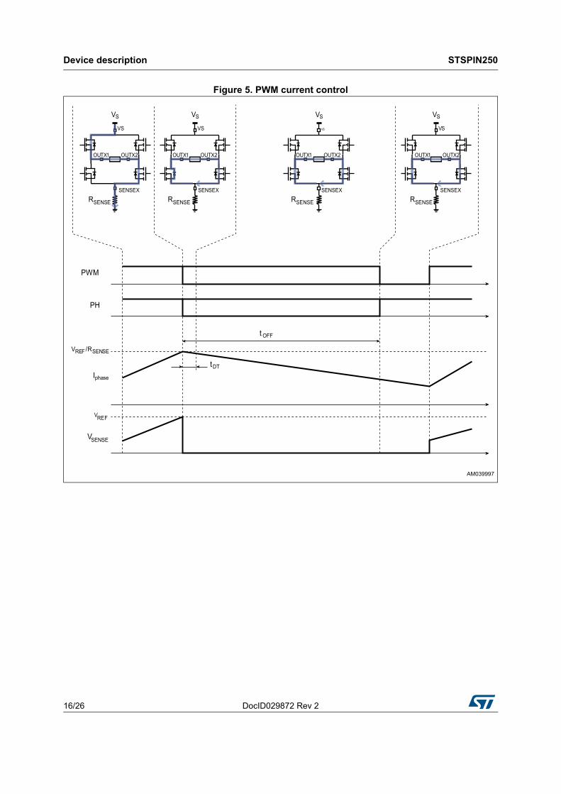
TOFF adjustment
The decay time is adjusted through an external resistor connected between the TOFF pin and ground as shown in Figure 6. A small RC series must be inserted in parallel with the regulator resistor in order to increase the stability of the regulation circuit according indications listed in Table 10.
Figure 6. OFF time regulation circuit
The relation between the OFF time and the external resistor value is shown in the graph of Figure 7. The value typically ranges from 10 µs to 150 µs.
Figure 7. OFF time vs ROFF value
Table 10. Recommended RRCOFF and CRCOFF values according to ROFF
ROFF RRCOFF CRCOFF
10 k ROFF < 82 k 1 k 22 nF
82 k ROFF 160 k 2.2 k 22 nF
Device description STSPIN250
18/26 DocID029872 Rev 2
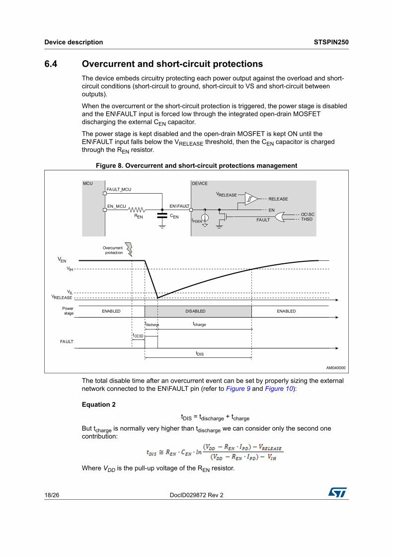
6.4 Overcurrent and short-circuit protections
The device embeds circuitry protecting each power output against the overload and short-circuit conditions (short-circuit to ground, short-circuit to VS and short-circuit between outputs).
When the overcurrent or the short-circuit protection is triggered, the power stage is disabled and the EN\FAULT input is forced low through the integrated open-drain MOSFET discharging the external CEN capacitor.
The power stage is kept disabled and the open-drain MOSFET is kept ON until the EN\FAULT input falls below the VRELEASE threshold, then the CEN capacitor is charged through the REN resistor.
Figure 8. Overcurrent and short-circuit protections management
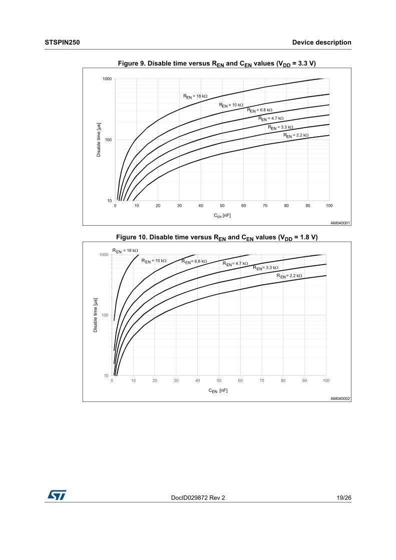
The total disable time after an overcurrent event can be set by properly sizing the external network connected to the EN\FAULT pin (refer to Figure 9 and Figure 10):
Equation 2
tDIS = tdischarge + tcharge
But tcharge is normally very higher than tdischarge we can consider only the second one contribution:
Where VDD is the pull-up voltage of the REN resistor.
DocID029872 Rev 2 19/26
STSPIN250 Device description
26
Figure 9. Disable time versus REN and CEN values (VDD = 3.3 V)
Figure 10. Disable time versus REN and CEN values (VDD = 1.8 V)
Device description STSPIN250
20/26 DocID029872 Rev 2
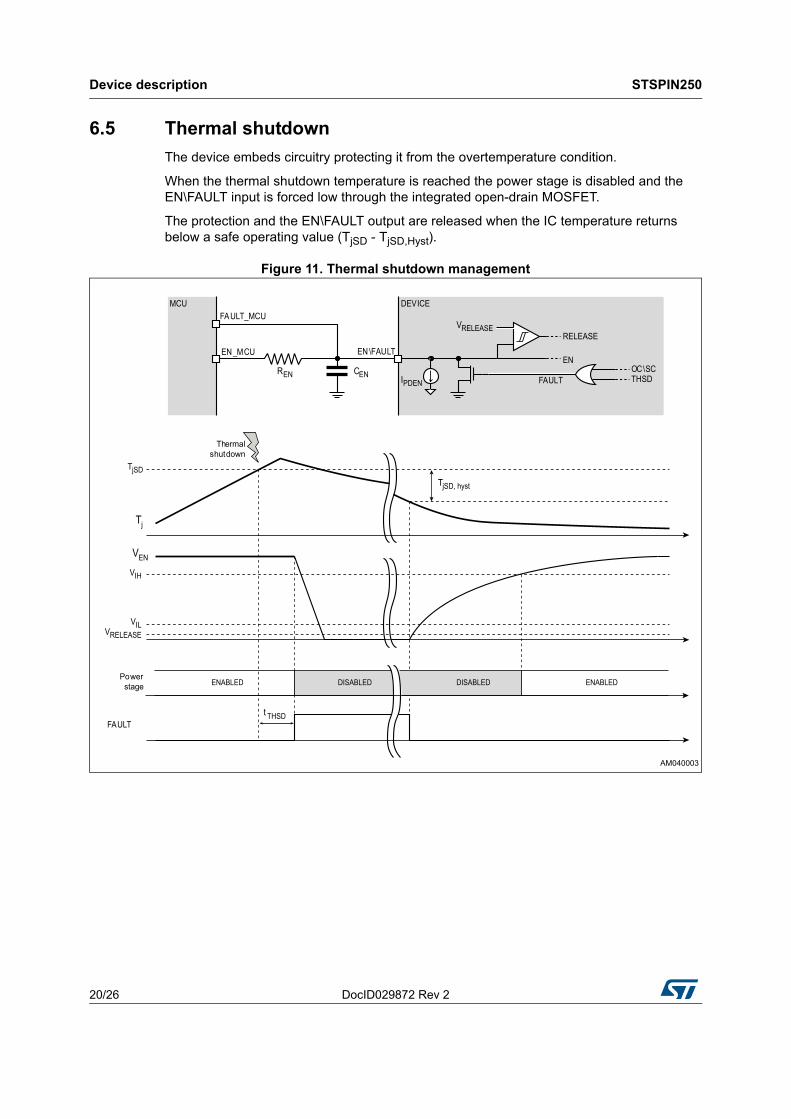
6.5 Thermal shutdown
The device embeds circuitry protecting it from the overtemperature condition.
When the thermal shutdown temperature is reached the power stage is disabled and the EN\FAULT input is forced low through the integrated open-drain MOSFET.
The protection and the EN\FAULT output are released when the IC temperature returns below a safe operating value (TjSD - TjSD,Hyst).
Figure 11. Thermal shutdown management
DocID029872 Rev 2 21/26
STSPIN250 Graphs
26
7 Graphs
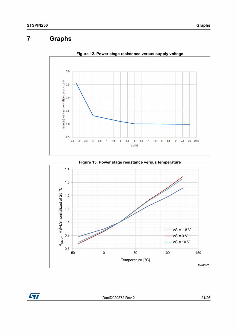
Figure 12. Power stage resistance versus supply voltage
Figure 13. Power stage resistance versus temperature
Graphs STSPIN250
22/26 DocID029872 Rev 2
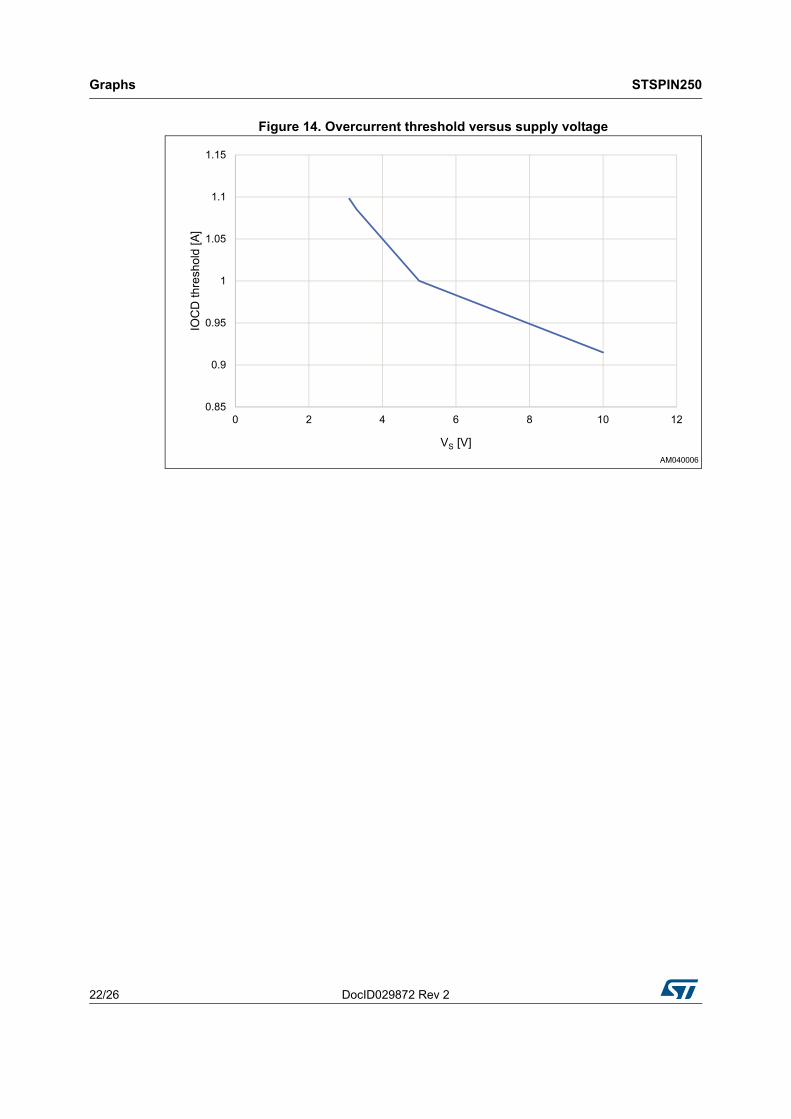
Figure 14. Overcurrent threshold versus supply voltage
DocID029872 Rev 2 23/26
STSPIN250 Package information
26
8 Package information
In order to meet environmental requirements, ST offers these devices in different grades of ECOPACK® packages, depending on their level of environmental compliance. ECOPACK® specifications, grade definitions and product status are available at: www.st.com. ECOPACK® is an ST trademark.
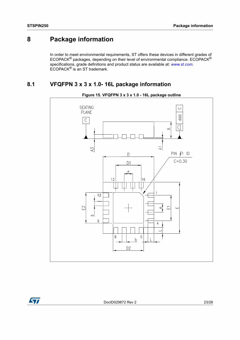
8.1 VFQFPN 3 x 3 x 1.0- 16L package information
Figure 15. VFQFPN 3 x 3 x 1.0 - 16L package outline
Package information STSPIN250
24/26 DocID029872 Rev 2
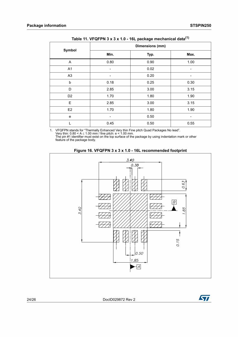
Figure 16. VFQFPN 3 x 3 x 1.0 - 16L recommended footprint
Table 11. VFQFPN 3 x 3 x 1.0 - 16L package mechanical data(1)
1. VFQFPN stands for “Thermally Enhanced Very thin Fine pitch Quad Packages No lead”.Very thin: 0.80 < A 1.00 mm / fine pitch: e < 1.00 mm.The pin #1 identifier must exist on the top surface of the package by using indentation mark or other feature of the package body.
SymbolDimensions (mm)
Min. Typ. Max.
A 0.80 0.90 1.00
A1 - 0.02 -
A3 - 0.20 -
b 0.18 0.25 0.30
D 2.85 3.00 3.15
D2 1.70 1.80 1.90
E 2.85 3.00 3.15
E2 1.70 1.80 1.90
e - 0.50 -
L 0.45 0.50 0.55
DocID029872 Rev 2 25/26
STSPIN250 Ordering information
26
9 Ordering information
10 Revision history
Table 12. Device summary
Order code Package Packaging
STSPIN250 VFQFPN 3 x 3 x1.0 - 16L Tape and reel
Table 13. Document revision history
Date Revision Changes
17-Oct-2016 1 Initial release.
04-Nov-2016 2
Updated document status to: Datasheet - production data on page 1.
Updated Figure 1 on page 5 and Figure 12 on page 21 (replaced by new figures).
Updated Table 2 on page 6 (added new parameter tINw).
Minor modifications throughout document.
STSPIN250
26/26 DocID029872 Rev 2
IMPORTANT NOTICE – PLEASE READ CAREFULLY
STMicroelectronics NV and its subsidiaries (“ST”) reserve the right to make changes, corrections, enhancements, modifications, and improvements to ST products and/or to this document at any time without notice. Purchasers should obtain the latest relevant information on ST products before placing orders. ST products are sold pursuant to ST’s terms and conditions of sale in place at the time of order acknowledgement.
Purchasers are solely responsible for the choice, selection, and use of ST products and ST assumes no liability for application assistance or the design of Purchasers’ products.
No license, express or implied, to any intellectual property right is granted by ST herein.
Resale of ST products with provisions different from the information set forth herein shall void any warranty granted by ST for such product.
ST and the ST logo are trademarks of ST. All other product or service names are the property of their respective owners.
Information in this document supersedes and replaces information previously supplied in any prior versions of this document.
© 2016 STMicroelectronics – All rights reserved