Functions of Combinational Logicrishiheerasing.net/modules/elec2102/ln/ss6.pdf · Slide Set 6...
41
Digital Electronics Functions of Combinational Logic
Transcript of Functions of Combinational Logicrishiheerasing.net/modules/elec2102/ln/ss6.pdf · Slide Set 6...
Digital Electronics
Functions of Combinational Logic

Slide Set 6 ELEC2103 2
Basic rules of binary addition are performed by a half adder, which has two binary inputs (A and B) and two binary outputs (Carry out and Sum).
Half-Adder
The inputs and outputs can be summarized on a truth table.
OutputsInputsA B C out Σ0011
0101
0 00 10 11 0
AB
Σ
Cout
The logic symbol and equivalent circuit are:
A
B
Σ
Cout
Σ

Slide Set 6 ELEC2103 3
Full-Adder
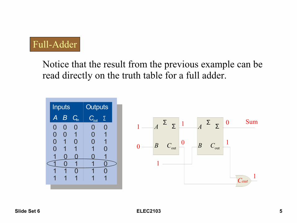
By contrast, a full adder has three binary inputs (A, B, and Carry in) and two binary outputs (Carry out and Sum). The truth table summarizes the operation.
OutputsInputsA B C out ΣCin
0
1
0
1
0
1
0
1
0
0
0
0
0
0
1
1
1
1
0
0
1
1
1
1
0
0
0
1
0
1
1
0
0
1
1
0
1
1
0
1
A full-adder can be constructed from two half adders as shown:
A
B
Σ
Cout
Σ A
B
Σ
Cout
ΣA
B
Sum
Cout
Cin
AB
Σ
Cout
Σ
Cin
Symbol

Slide Set 6 ELEC2103 4
Full-AdderA
B
Σ
Cout
Σ A
B
Σ
Cout
Σ
For the given inputs, determine the intermediate and final outputs of the full adder.
1
1
0
1
0
The first half-adder has inputs of 1 and 0; therefore the Sum =1 and the Carry out = 0.
The second half-adder has inputs of 1 and 1; therefore the Sum = 0 and the Carry out = 1.
The OR gate has inputs of 1 and 0, therefore the final carry out = 1.
1
0
1
Sum
Cout
Slide Set 6 ELEC2103 5
Full-Adder
OutputsInputsA B C out ΣCin
0
1
0
1
0
1
0
1
0
0
0
0
0
0
1
1
1
1
0
0
1
1
1
1
0
0
0
1
0
1
1
0
0
1
1
0
1
1
0
1
A
B
Σ
Cout
Σ A
B
Σ
Cout
Σ1
1
0
1
0 1
0
1
Sum
Cout
Notice that the result from the previous example can be read directly on the truth table for a full adder.
Slide Set 6 ELEC2103 6
Parallel Adders
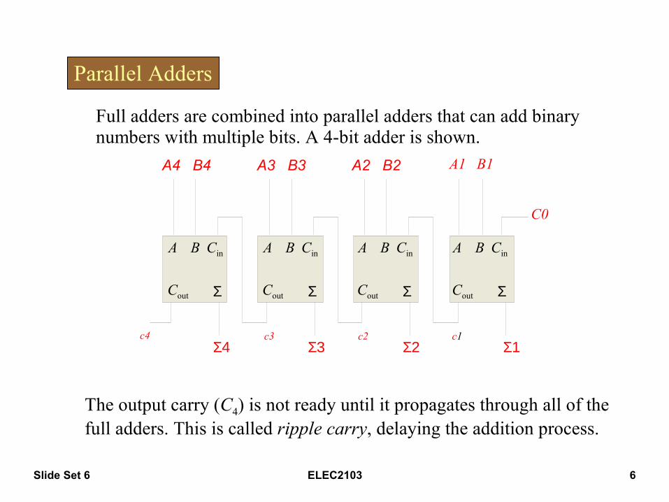
Full adders are combined into parallel adders that can add binary numbers with multiple bits. A 4-bit adder is shown.
A B
ΣCout
Cin A B
ΣCout
Cin A B
ΣCout
Cin A B
ΣCout
Cin
A1 B1
Σ1
C0
Σ2Σ3Σ4c1c2c3c4
The output carry (C4) is not ready until it propagates through all of the full adders. This is called ripple carry, delaying the addition process.
A2 B2A3 B3A4 B4

Slide Set 6 ELEC2103 7
Parallel AddersThe logic symbol for a 4-bit parallel adder is shown. This 4-bit adder includes a carry in (labeled (C0) and a Carry out (labeled C4).
The 74LS283 is an example. It features look-ahead carry, which adds logic to minimize the output carry delay. For the 74LS283, the maximum delay to the output carry is 17 ns.
Binary number A
Binary number B
Input carry
4-bit sum
Output carry
1234
1234
1234
C0 C4
Σ

Slide Set 6 ELEC2103 8
ComparatorsThe function of a comparator is to compare the magnitudes of two binary numbers to determine the relationship between them. In the simplest form, a comparator can test for equality using XNOR gates.
How could you test two 4-bit numbers for equality?
AND the outputs of four XNOR gates.
A2B2
A1B1
A4B4
A3B3
Output

Slide Set 6 ELEC2103 9
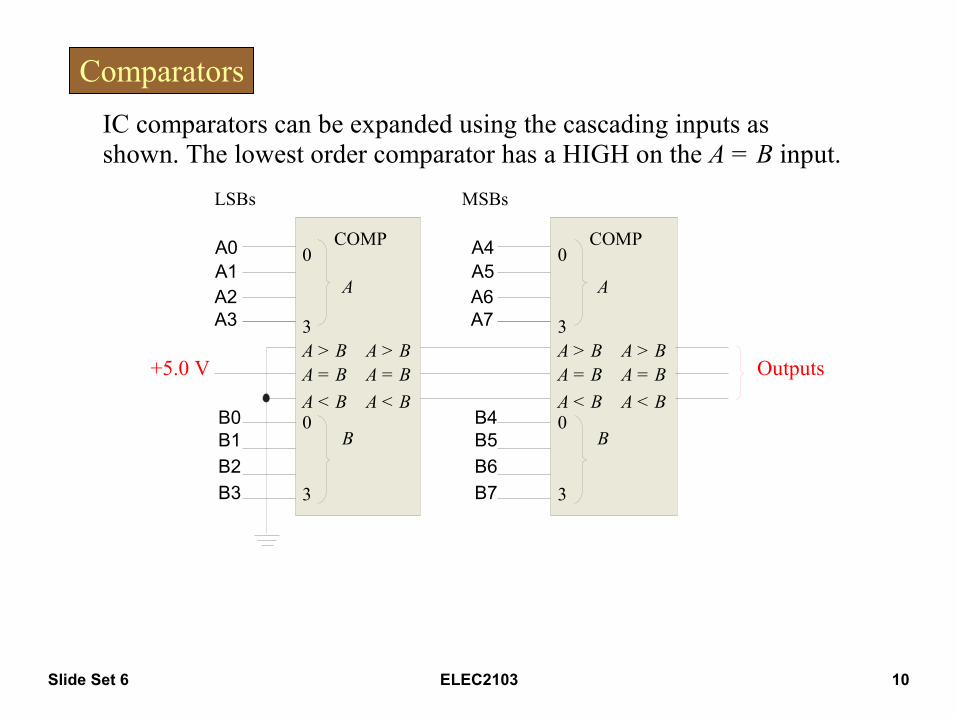
ComparatorsIC comparators provide outputs to indicate which of the numbers is larger or if they are equal. The bits are numbered starting at 0, rather than 1 as in the case of adders. Cascading inputs are provided to expand the comparator to larger numbers.
OutputsCascading inputs
COMP
A = BA < B
A > BA = BA < B
A > B
0
0
3
3
A
BThe IC shown is the 4-bit 74LS85.B3
B0
A3A2A1A0
B2B1
Slide Set 6 ELEC2103 10
ComparatorsIC comparators can be expanded using the cascading inputs as shown. The lowest order comparator has a HIGH on the A = B input.
Outputs
COMP
A = BA < B
A > BA = BA < B
A > B
0
0
3
3
A
B
+5.0 V
COMP
A = BA < B
A > BA = BA < B
A > B
0
0
3
3
A
B
LSBs MSBs
B3
B0
A3A2A1A0
B2B1
B7
B4
A7A6A5A4
B6B5

Slide Set 6 ELEC2103 11
DecodersA decoder is a logic circuit that detects the presence of a specific combination of bits at its input. Two simple decoders that detect the presence of the binary code 0011 are shown. The first has an active HIGH output; the second has an active LOW output.
X
Active HIGH decoder for 0011
X
Active LOW decoder for 0011
A3
A2
A1
A0
A3
A2
A1
A0
Slide Set 6 ELEC2103 12
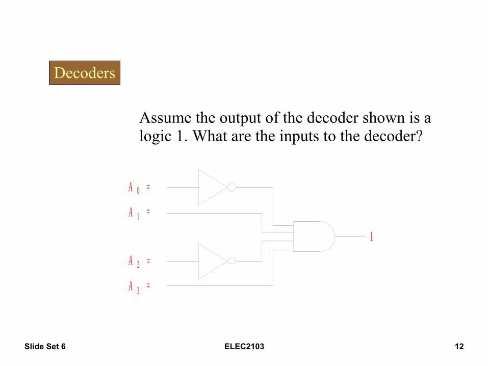
Decoders
A 0 = 0
A 1 = 1
A 2 = 0
A 3 = 1
1
Assume the output of the decoder shown is a logic 1. What are the inputs to the decoder?

Slide Set 6 ELEC2103 13
DecodersIC decoders have multiple outputs to decode any combination of inputs. For example the binary-to-decimal decoder shown here has 16 outputs – one for each combination of binary inputs.
B i n / D e c
A 0
0123456789
1 01 11 21 31 41 5
4 - b i t b i n a r yi n p u t
D e c i m a lo u t p u t s
A 1
A 2
A 3
110
1111111111101111
1
1
0
1
1
For the input shown, what is the output?

Slide Set 6 ELEC2103 14
Decoders
A specific integrated circuit decoder is the 74HC154 (shown as a 4-to-16 decoder). It includes two active LOW chip select lines which must be at the active level to enable the outputs. These lines can be used to expand the decoder to larger inputs.
CS215
121314
1234
91011
5678
0
&
48
12
CS1
X/Y
EN
74HC154
A3A2A1A0
Slide Set 6 ELEC2103 15
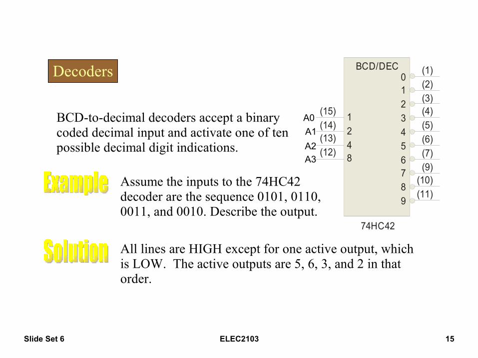
Decoders
BCD-to-decimal decoders accept a binary coded decimal input and activate one of ten possible decimal digit indications.
BCD/DEC0123456789
1248
74HC42
(11)(10)
(9)(7)(6)(5)(4)(3)(2)(1)
(15)(14)(13)(12)
Assume the inputs to the 74HC42 decoder are the sequence 0101, 0110, 0011, and 0010. Describe the output.
All lines are HIGH except for one active output, which is LOW. The active outputs are 5, 6, 3, and 2 in that order.
A3A2A1A0
Slide Set 6 ELEC2103 16
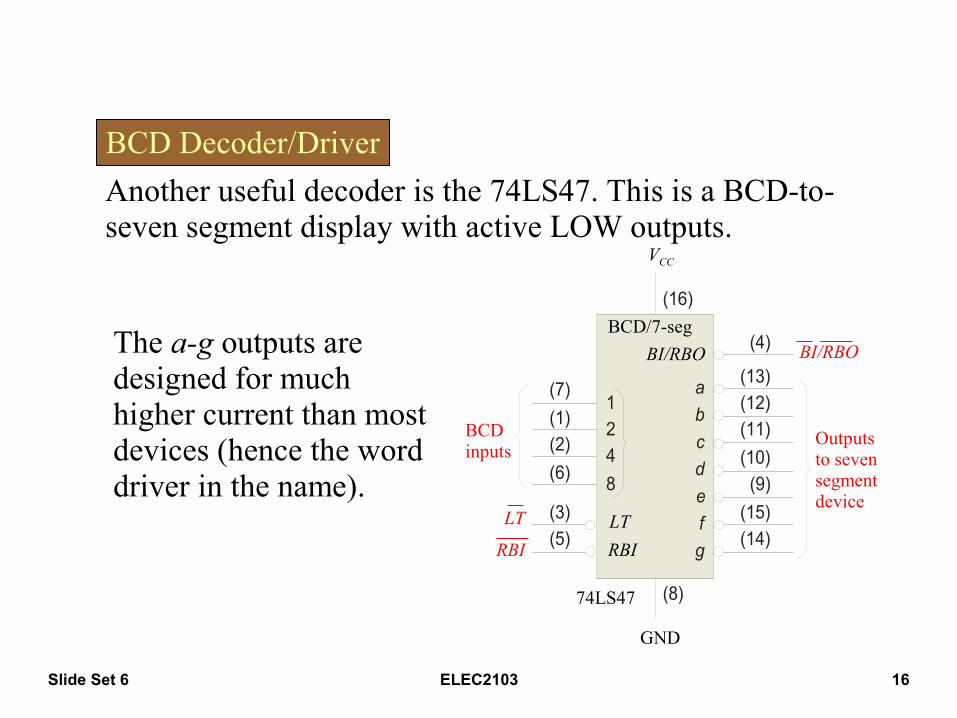
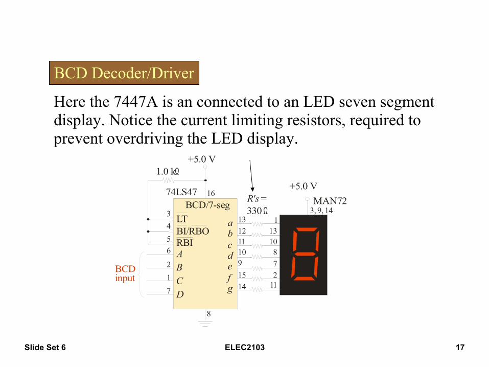
BCD Decoder/DriverAnother useful decoder is the 74LS47. This is a BCD-to-seven segment display with active LOW outputs.
The a-g outputs are designed for much higher current than most devices (hence the word driver in the name).
abcdefg
1248
(16)
(4)
(13)(12)(11)(10)
(9)(15)(14)
(1)(2)(6)
(7)
(3)(5)
(8)
BCD inputs
Outputs to seven segment device
GND
VCC
BCD/7-segBI/RBO BI/RBO
LTRBI
LT
RBI
74LS47
Slide Set 6 ELEC2103 17
BCD Decoder/Driver
Here the 7447A is an connected to an LED seven segment display. Notice the current limiting resistors, required to prevent overdriving the LED display.
VC C
GND
+5.0 V
+5.0 V
R's =330 Ω
abcdefg
abcdefg
MAN7274LS47
LTBI/RBORBI
1.0 kΩ
1
1 22
3, 9, 143456
7
7
8
8
9
1010
11
1112 1313
1415
16BCD/7-seg
BCDinput
DCBA
Slide Set 6 ELEC2103 18
BCD Decoder/Driver
abcdefg BI/RBO
0 0 0 0
8 4 2 1RBI LT
0
74LS47
abcdefg BI/RBO
0 0 0 0
8 4 2 1RBI LT
0
74LS47
abcdefg BI/RBO
0 0 1 1
8 4 2 1RBI LT
0
74LS47
abcdefg BI/RBO
0 0 0 0
8 4 2 1RBI LT
1
74LS47
Blanked Blanked
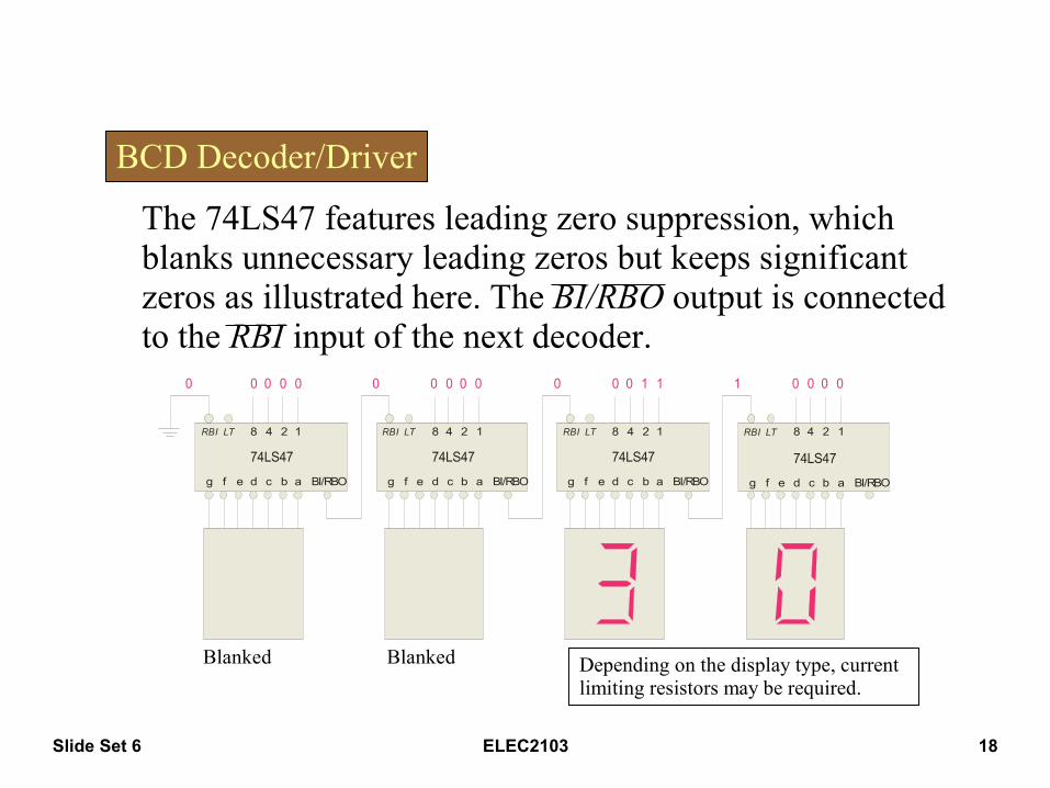
The 74LS47 features leading zero suppression, which blanks unnecessary leading zeros but keeps significant zeros as illustrated here. The BI/RBO output is connected to the RBI input of the next decoder.
Depending on the display type, current limiting resistors may be required.

Slide Set 6 ELEC2103 19
BCD Decoder/Driver
Blanked Blanked
abcdefg BI/RBO
0 1 0 1
8 4 2 1RBI LT
74LS47
1
abcdefg BI/RBO
0 1 1 1
8 4 2 1RBI LT
74LS47
abcdefg BI/RBO
0 0 0 0
8 4 2 1RBI LT
74LS47
0
abcdefg BI/RBO
0 0 0 0
8 4 2 1RBI LT
74LS47
0
Decimal point
Trailing zero suppression blanks unnecessary trailing zeros to the right of the decimal point as illustrated here. The RBI input is connected to the BI/RBO output of the following decoder.

Slide Set 6 ELEC2103 20
Encoders
An encoder accepts an active logic level on one of its inputs and converts it to a coded output, such as BCD or binary. The decimal to BCD is an encoder with an input for each of the ten decimal digits and four outputs that represent the BCD code for the active digit. The basic logic diagram is shown. There is no zero input because the outputs are all LOW when the input is zero.
1
2
3
45678
9A3
A2
A1
A0
Slide Set 6 ELEC2103 21
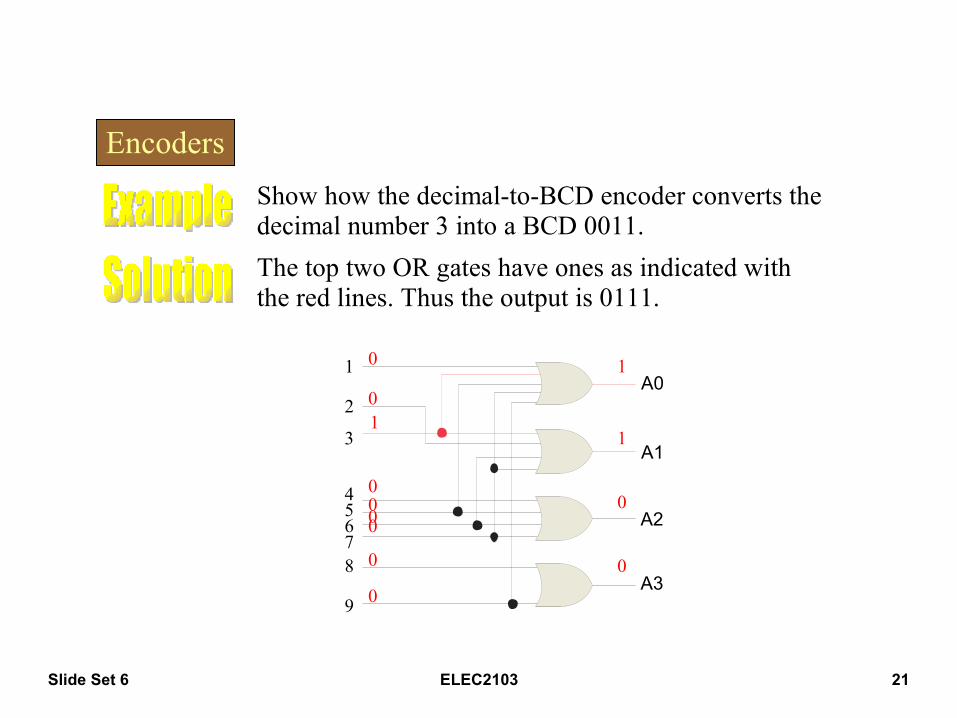
EncodersShow how the decimal-to-BCD encoder converts the decimal number 3 into a BCD 0011.The top two OR gates have ones as indicated with the red lines. Thus the output is 0111.
1
2
3
45678
9
0
0
0
000
0
0
1
0
0
1
1
A3
A2
A1
A0
Slide Set 6 ELEC2103 22
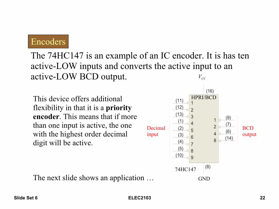
EncodersThe 74HC147 is an example of an IC encoder. It is has ten active-LOW inputs and converts the active input to an active-LOW BCD output.
This device offers additional flexibility in that it is a priority encoder. This means that if more than one input is active, the one with the highest order decimal digit will be active.
Decimal input
BCD output
1248
(16)
(11)(12)(13)(1)(2)
(4)(3)
(5)
(9)(7)(6)(14)
(8)
12345678
(10) 9
GND
VCC
HPRI/BCD
74HC147
The next slide shows an application …

Slide Set 6 ELEC2103 23
EncodersVCC
BCD complement of key press
123456789
1248
987
65
321
0
4
R7 R8 R9
R4 R5 R6
R1 R2 R3
R0
Keyboard encoder HPRI/BCD
74HC147
The zero line is not needed by the encoder, but may be used by other circuits to detect a key press.

Slide Set 6 ELEC2103 24
Code converters
There are various code converters that change one code to another. Two examples are the four bit binary-to-Gray converter and the Gray-to-binary converter.
Show the conversion of binary 0111 to Gray and back.
00
0
1
1
1
Binary-to-Gray Gray-to-BinaryMSB
LSB
MSB
LSB
1
0
0
0
1
0
0
1
1
1

Slide Set 6 ELEC2103 25
MUX
12
0
3
10
A multiplexer (MUX) selects one data line from two or more input lines and routes data from the selected line to the output. The particular data line that is selected is determined by the select inputs.
Multiplexers
Two select lines are shown here to choose any of the four data inputs.
Data select
Data inputs
Data outputD1
D0
D2D3
S1S0
Which data line is selected if S1S0 = 10? D2
1
0
Slide Set 6 ELEC2103 26
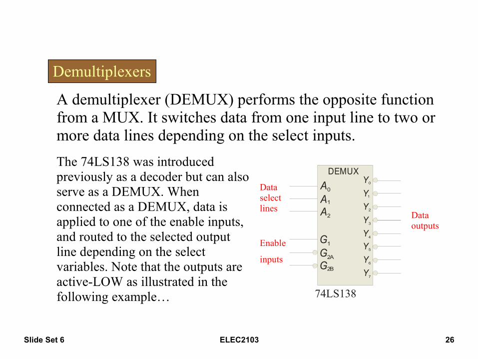
A demultiplexer (DEMUX) performs the opposite function from a MUX. It switches data from one input line to two or more data lines depending on the select inputs. The 74LS138 was introduced previously as a decoder but can also serve as a DEMUX. When connected as a DEMUX, data is applied to one of the enable inputs, and routed to the selected output line depending on the select variables. Note that the outputs are active-LOW as illustrated in the following example…
Demultiplexers
74LS138
Y1
Y2
Y3
Y4
Y5
Y6
Y7
Y0
DEMUXAAA
0
1
2
GGG
1
2A
2B
Data select lines
Enable
inputs
Data outputs
Slide Set 6 ELEC2103 27
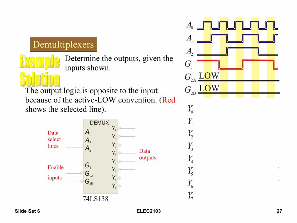
Determine the outputs, given the inputs shown.
Demultiplexers
74LS138
Y1
Y2
Y3
Y4
Y5
Y6
Y7
Y0
DEMUXAAA
0
1
2
GGG
1
2A
2B
Data select lines
Enable
inputs
Data outputs
A0
Y0
Y1
Y2
Y3
Y4
Y5
Y6
Y7
A1
A2
G1
G2A
G2B
LOWLOWThe output logic is opposite to the input
because of the active-LOW convention. (Red shows the selected line).
Slide Set 6 ELEC2103 28
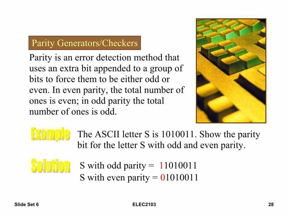
Parity Generators/CheckersParity is an error detection method that uses an extra bit appended to a group of bits to force them to be either odd or even. In even parity, the total number of ones is even; in odd parity the total number of ones is odd.
11010011S with odd parity =S with even parity = 01010011
The ASCII letter S is 1010011. Show the parity bit for the letter S with odd and even parity.

Slide Set 6 ELEC2103 29
Parity Generators/CheckersThe 74LS280 can be used to generate a parity bit or to check an incoming data stream for even or odd parity. Checker: The 74LS280 can test codes with up to 9 bits. The even output will normally be HIGH if the data lines have even parity; otherwise it will be LOW. Likewise, the odd output will normally be HIGH if the data lines have odd parity; otherwise it will be LOW.
Generator: To generate even parity, the parity bit is taken from the odd parity output. To generate odd parity, the output is taken from the even parity output.
(5)(6)
(13)(1)
(11)(12)
(2)
(10)(9)(8)
FG
DE
H
CBA
(4)I
74LS280
Data inputs
Σ EvenΣ Odd
Selected Key TermsSelected Key Terms
Full-adder
Cascading
Ripple carry
Look-ahead carry
A digital circuit that adds two bits and an input carry bit to produce a sum and an output carry.
Connecting two or more similar devices in a manner that expands the capability of one device.
A method of binary addition in which the output carry from each adder becomes the input carry of the next higher order adder.
A method of binary addition whereby carries from the preceding adder stages are anticipated, thus eliminating carry propagation delays.

Selected Key TermsSelected Key Terms
Decoder
Encoder
Priority encoder
Multiplexer (MUX)
Demultiplexer (DEMUX)
A digital circuit that converts coded information into a familiar or noncoded form.
A digital circuit that converts information into a coded form.
An encoder in which only the highest value input digit is encoded and any other active input is ignored.
A circuit that switches digital data from several input lines onto a single output line in a specified time sequence.
A circuit that switches digital data from one input line onto a several output lines in a specified time sequence.
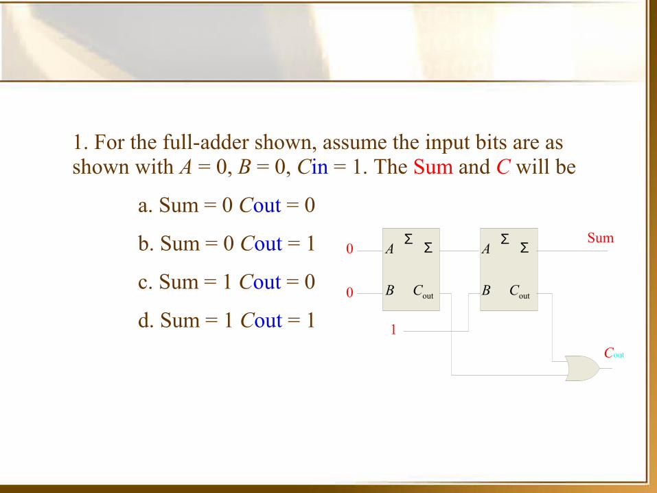
1. For the full-adder shown, assume the input bits are as shown with A = 0, B = 0, Cin = 1. The Sum and C will be
a. Sum = 0 Cout = 0
b. Sum = 0 Cout = 1
c. Sum = 1 Cout = 0
d. Sum = 1 Cout = 1
A
B
Σ
Cout
Σ A
B
Σ
Cout
Σ0
1
0
Sum
Cout

2. The output will be LOW if
a. A < B
b. A > B
c. both a and b are correct
d. A = B
OutputA2B2
A1B1
A4B4
A3B3
3. If you expand two 4-bit comparators to accept two 8-bit numbers, the output of the least significant comparator is
a. equal to the final output
b. connected to the cascading inputs of the most significant comparator
c. connected to the output of the most significant comparator
d. not used

4. Assume you want to decode the binary number 0011 with an active-LOW decoder. The missing gate should be
a. an AND gate
b. an OR gate
c. a NAND gate
d. a NOR gate
A1
A0
A2
A3
X?
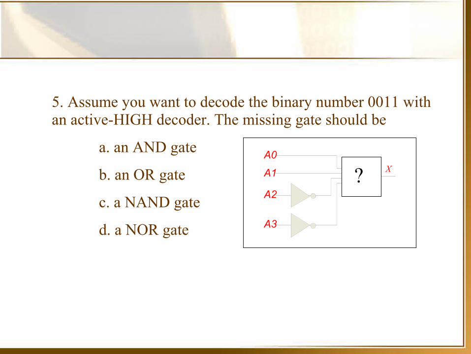
5. Assume you want to decode the binary number 0011 with an active-HIGH decoder. The missing gate should be
a. an AND gate
b. an OR gate
c. a NAND gate
d. a NOR gate
X?A1
A0
A2
A3

6. The 74138 is a 3-to-8 decoder. Together, two of these ICs can be used to form one 4-to-16 decoder. To do this, connect
a. one decoder to the LSBs of the input; the other decoder to the MSBs of the input
b. all chip select lines to ground
c. all chip select lines to their active levels
d. one chip select line on each decoder to the input MSB

7. The decimal-to-binary encoder shown does not have a zero input. This is because
a. when zero is the input, all lines should be LOW
b. zero is not important
c. zero will produce illegal logic levelsd. another encoder is used for zero
1
2
3
45678
9
A1
A0
A2
A3

8. If the data select lines of the MUX are S1S0 = 11, the output will be
a. LOW
b. HIGH
c. equal to D0
d. equal to D3
MUX
12
0
3
10
Data output
Data select
Data inputs
D1D0
D2
D3
S1S0
9. The 74138 decoder can also be used as
a. an encoder
b. a DEMUX
c. a MUX
d. none of the above
10. The 74LS280 can generate even or odd parity. It can also be used as
a. an adder
b. a parity tester
c. a MUX
d. an encoder
© 2009 Pearson Education