


γλώσσες
Σελίδες
Νομικός

Q-band VCOfor 77-GHz
in
Jae-hoon Song, Sangwook NSchool of Electrical Engineering & Comp
Seoul National University, Seoul, Republic of Korea
Abstract —This paper includes Q-band VCOpower injection-locked buffer for 77-GHz FMin 0.13-µm CMOS process. The center frequenVCO is 34.75-GHz with 1.6% tuning range. Tnoise performance shows -102.43 dBc/Hz frequency. The measured maximum single oudBm and the ideal differential output power isdBm, owing to the injection-locked buffer wcapability. The fabricated chip size is 0.51 × 0.1consumption of the VCO core and the injection10.8 mW and 50.4 mW from a 1.2 V supply, r
Key words: Q-band VCO, Injection-lockeAutomotive radar, CMOS
I. INTRODUCTION In millimeter-wave automotive radar sy
semiconductors have been widely used dubreakdown voltage [1], [2]. However, the conductor has limitations of its higher integration property than CMOS technology77-GHz radar system. As performance of Cbeen recently improved, CMOS technology h77-GHz automotive radar systems [3], [4]. Rbe classified largely into two categories accoof wave transmission. One is pulse radar continuous-wave radar. For pulse radar, it reto-average power ratio (PAPR) and widebgenerate output short pulse in time-domainprocess is difficult to be applied in millimetersystem because of relatively low supply vdevices. Thus, frequency modulated continuoradar can be a proper candidate for 77-GHzsystem in CMOS process. In the FMCW, oissues is to generate 77-GHz signal. One waGHz signal is designing 77-GHz oscillatorother way is designing 77/N-GHz oscillator with frequency multiplier. Fig. 1 shows a conFMCW radar transmitter with a 38.5-Gfrequency multiplier [5]. In this paper, wVCO and high output power injection-lockedserves as DA. Section II explains circuit proposed VCO and the injection-locked buf
-
Figure 1. A concept of 77-G
O and Injection-lockedz Automotive Radar Sn 0.13-µm CMOS
Nam puter Science,
Seong-Kyun KimSchool of Information and
SungkyunkwSuwon, Rep
O and high output MCW radar system ncy of the proposed he measured phase
at 1-MHz offset utput power is 5.2 s expected to be 8.2
with a high driving 13 mm2. The power n-locked buffer are respectively.
ed buffer, FMCW,
ystems, compound ue to high fT and
compound semi-cost and lower
when applying to CMOS device has has been applied to Radar systems can ording to principle
and the other is equires high peak-band operation to n, so that CMOS r-wave pulse radar voltage of CMOS ous-wave (FMCW) z automotive radar one of challenging ay to generate 77-r directly and the and multiplying N ncept of a 77-GHz
GHz VCO and a we present Q-band d buffer which can description of the
ffer. In Section III,
measurement results are presenup in Section IV.
II. CIRCUI
In this section, the proposebuffer is described. In general, should be placed between Vsince common VCO buffer cato operate the frequency muhigh-power injection-locked btwo blocks, a buffer and a DA,
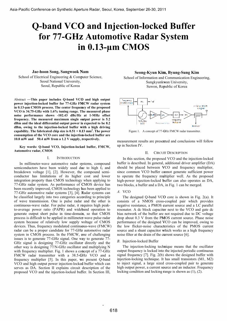
A. VCO The designed Q-band VCO
consists of a NMOS cross-negative resistance, a PMOS cresonator. A dc block capacitobias network of the buffer are drop about 0.3 V from the PMperformance of the designed Vthe low flicker-noise charactsource and a shunt capacitor wnoise filter at the drain of the cu
B. Injection-locked Buffer The injection-locking techn
output frequency is locked into signal frequency [7]. Fig. 2(b) injection-locking technique. It to inject signal, a large sized high output power, a current solocking condition and locking r
GHz FMCW radar transmitter.
d Buffer System
m, Byung-Sung Kim Communication Engineering,
wan University, public of Korea
nted and conclusions will follow
IT DESCRIPTION d VCO and the injection-locked additional driver amplifier (DA)
VCO and frequency multiplier, annot generate sufficient power ultiplier well. As the proposed buffer can also operates as DA,
in Fig. 1 can be merged.
O core is shown in Fig. 2(a). It -coupled pair which provides current source and a LC parallel or next to the VCO and gate dc not required due to DC voltage
MOS current source. Phase noise VCO can be improved, owing to teristics of the PMOS current
which works as a high frequency urrent source [6].
nique means that the oscillator the injected periodic continuous shows the designed buffer with has small transistors (M1, M2) cross-coupled pair to generate
ource and an inductor. Frequency range is shown as (1), (2).
618
(a)
(b)
Figure 3. (a) VCO schematic. (b) Injection-locking
|| 0 lockinj ωωω Δ<−
AA
Qinj
lock 20ωω =Δ
ω and ω are the frequency of the inthe frequency of the oscillator, respectively. Alocking range. In case of the proposed cirsignal is the VCO output signal and the osciwhich oscillates in the steady-state. The injecoutput frequency is locked into VCO outputhrough M1, M2 when (1) is satisfied [8]. Thinductor value should be decided to resonateof the cross-coupled pair in the vicinity of thfrequency in order to fulfill the locking conthe locking range can be written with ω , Qand the amplitude of the injected signal and signal injection transistors, M1, M2, can prpower of the buffer from leaking into the Vits small size. It also operates as the DA, provides high output power due to relatively
-
buffer schematic.
(a)
(b)
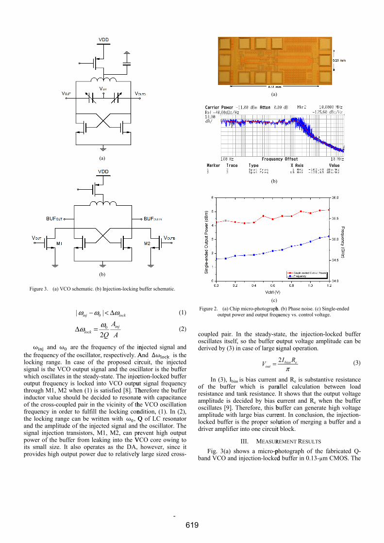
(c) Figure 2. (a) Chip micro-photograph
output power and output frequ
(1)
(2)
njected signal and And ∆ω is the rcuit, the injected illator is the buffer ction-locked buffer ut signal frequency herefore the buffer e with capacitance
he VCO oscillation ndition, (1). In (2), Q of LC resonator the oscillator. The
revent high output VCO core owing to
however, since it y large sized cross-
coupled pair. In the steady-stoscillates itself, so the buffer oderived by (3) in case of large s
outV =
In (3), Ibias is bias current of the buffer which is pararesistance and tank resistance. amplitude is decided by bias coscillates [9]. Therefore, this bamplitude with large bias currelocked buffer is the proper soludriver amplifier into one circuit
III. MEASUR
Fig. 3(a) shows a micro-pband VCO and injection-locked
h. (b) Phase noise. (c) Single-ended uency vs. control voltage.
ate, the injection-locked buffer output voltage amplitude can be signal operation.
πebiasRI2
(3)
and Re is substantive resistance allel calculation between load It shows that the output voltage current and Re when the buffer buffer can generate high voltage ent. In conclusion, the injection-ution of merging a buffer and a t block.
REMENT RESULTS photograph of the fabricated Q-d buffer in 0.13-µm CMOS. The
619
-
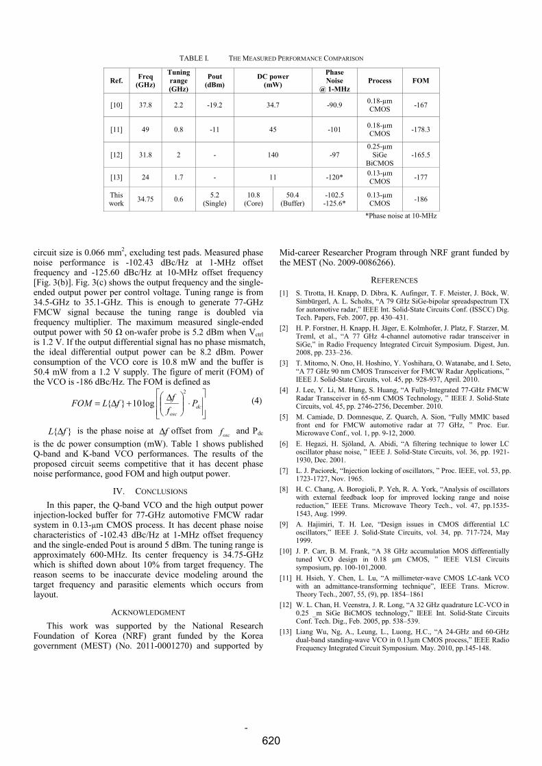
TABLE I. THE MEASURED PERFORMANCE COMPARISON
Ref. Freq (GHz)
Tuning range (GHz)
Pout (dBm)
DC power (mW)
Phase Noise
@ 1-MHz Process FOM
[10] 37.8 2.2 -19.2 34.7 -90.9 0.18-µm CMOS -167
[11] 49 0.8 -11 45 -101 0.18-µm CMOS -178.3
[12] 31.8 2 - 140 -97 0.25-µm
SiGe BiCMOS
-165.5
[13] 24 1.7 - 11 -120* 0.13-µm CMOS -177
This work 34.75 0.6 5.2
(Single) 10.8
(Core) 50.4
(Buffer) -102.5
-125.6* 0.13-µm CMOS -186
*Phase noise at 10-MHz
circuit size is 0.066 mm2, excluding test pads. Measured phase noise performance is -102.43 dBc/Hz at 1-MHz offset frequency and -125.60 dBc/Hz at 10-MHz offset frequency [Fig. 3(b)]. Fig. 3(c) shows the output frequency and the single-ended output power per control voltage. Tuning range is from 34.5-GHz to 35.1-GHz. This is enough to generate 77-GHz FMCW signal because the tuning range is doubled via frequency multiplier. The maximum measured single-ended output power with 50 Ω on-wafer probe is 5.2 dBm when Vctrl is 1.2 V. If the output differential signal has no phase mismatch, the ideal differential output power can be 8.2 dBm. Power consumption of the VCO core is 10.8 mW and the buffer is 50.4 mW from a 1.2 V supply. The figure of merit (FOM) of the VCO is -186 dBc/Hz. The FOM is defined as
⎥⎥⎦
⎤
⎢⎢⎣
⎡⋅⎟⎟
⎠
⎞⎜⎜⎝
⎛ Δ+Δ= dcosc
PfffLFOM
2
log10 (4)
fL Δ is the phase noise at fΔ offset from oscf and Pdc is the dc power consumption (mW). Table 1 shows published Q-band and K-band VCO performances. The results of the proposed circuit seems competitive that it has decent phase noise performance, good FOM and high output power.
IV. CONCLUSIONS In this paper, the Q-band VCO and the high output power
injection-locked buffer for 77-GHz automotive FMCW radar system in 0.13-µm CMOS process. It has decent phase noise characteristics of -102.43 dBc/Hz at 1-MHz offset frequency and the single-ended Pout is around 5 dBm. The tuning range is approximately 600-MHz. Its center frequency is 34.75-GHz which is shifted down about 10% from target frequency. The reason seems to be inaccurate device modeling around the target frequency and parasitic elements which occurs from layout.
ACKNOWLEDGMENT This work was supported by the National Research
Foundation of Korea (NRF) grant funded by the Korea government (MEST) (No. 2011-0001270) and supported by
Mid-career Researcher Program through NRF grant funded by the MEST (No. 2009-0086266).
REFERENCES [1] S. Ttrotta, H. Knapp, D. Dibra, K. Aufinger, T. F. Meister, J. Böck, W.
Simbürgerl, A. L. Scholts, “A 79 GHz SiGe-bipolar spreadspectrum TX for automotive radar,” IEEE Int. Solid-State Circuits Conf. (ISSCC) Dig. Tech. Papers, Feb. 2007, pp. 430–431.
[2] H. P. Forstner, H. Knapp, H. Jäger, E. Kolmhofer, J. Platz, F. Starzer, M. Treml, et al., “A 77 GHz 4-channel automotive radar transceiver in SiGe,” in Radio Frequency Integrated Circuit Symposium. Digest, Jun. 2008, pp. 233–236.
[3] T. Mitomo, N. Ono, H. Hoshino, Y. Yoshihara, O. Watanabe, and I. Seto, “A 77 GHz 90 nm CMOS Transceiver for FMCW Radar Applications, ” IEEE J. Solid-State Circuits, vol. 45, pp. 928-937, April. 2010.
[4] J. Lee, Y. Li, M. Hung, S. Huang, “A Fully-Integrated 77-GHz FMCW Radar Transceiver in 65-nm CMOS Technology, ” IEEE J. Solid-State Circuits, vol. 45, pp. 2746-2756, December. 2010.
[5] M. Camiade, D. Domnesque, Z. Quarch, A. Sion, “Fully MMIC based front end for FMCW automotive radar at 77 GHz, ” Proc. Eur. Microwave Conf., vol. 1, pp. 9-12, 2000.
[6] E. Hegazi, H. Sjöland, A. Abidi, “A filtering technique to lower LC oscillator phase noise, ” IEEE J. Solid-State Circuits, vol. 36, pp. 1921-1930, Dec. 2001.
[7] L. J. Paciorek, “Injection locking of oscillators, ” Proc. IEEE, vol. 53, pp. 1723-1727, Nov. 1965.
[8] H. C. Chang, A. Borogioli, P. Yeh, R. A. York, “Analysis of oscillators with external feedback loop for improved locking range and noise reduction,” IEEE Trans. Microwave Theory Tech., vol. 47, pp.1535-1543, Aug. 1999.
[9] A. Hajimiri, T. H. Lee, “Design issues in CMOS differential LC oscillators,” IEEE J. Solid-State Circuits, vol. 34, pp. 717-724, May 1999.
[10] J. P. Carr, B. M. Frank, “A 38 GHz accumulation MOS differentially tuned VCO design in 0.18 μm CMOS, ” IEEE VLSI Circuits symposium, pp. 100-101,2000.
[11] H. Hsieh, Y. Chen, L. Lu, “A millimeter-wave CMOS LC-tank VCO with an admittance-transforming technique”, IEEE Trans. Microw. Theory Tech., 2007, 55, (9), pp. 1854–1861
[12] W. L. Chan, H. Veenstra, J. R. Long, “A 32 GHz quadrature LC-VCO in 0.25 _m SiGe BiCMOS technology,” IEEE Int. Solid-State Circuits Conf. Tech. Dig., Feb. 2005, pp. 538–539.
[13] Liang Wu, Ng, A., Leung, L., Luong, H.C., “A 24-GHz and 60-GHz dual-band standing-wave VCO in 0.13µm CMOS process,” IEEE Radio Frequency Integrated Circuit Symposium. May. 2010, pp.145-148.
620
Top Related