


γλώσσες
Σελίδες
Νομικός

Induction of tin pest for cleaning tin-drop contaminated optics
Norbert Böweringa,b*
aBökoTech, Ringstraße 21, 33619 Bielefeld, Germany and
bMolecular and Surface Physics, Bielefeld University, 33501 Bielefeld, Germany
Highlights
Tin pest induction leads to embrittlement of tin drops after β → α Sn transformation.
The purity grade influences the transformation speed of tin very strongly.
Tin drops on multilayer-coated optics disintegrate after β → α Sn transformation.
Tin drop contamination of optics is cleaned via phase transformation at -24 °C.
Reflectance of multilayer-coated mirrors is restored after tin drop transformation.
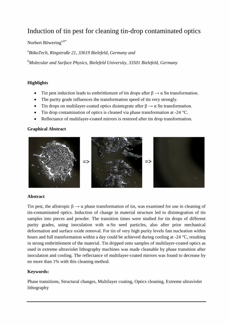
Graphical Abstract
Abstract
Tin pest, the allotropic β → α phase transformation of tin, was examined for use in cleaning of
tin-contaminated optics. Induction of change in material structure led to disintegration of tin
samples into pieces and powder. The transition times were studied for tin drops of different
purity grades, using inoculation with α-Sn seed particles, also after prior mechanical
deformation and surface oxide removal. For tin of very high purity levels fast nucleation within
hours and full transformation within a day could be achieved during cooling at -24 °C, resulting
in strong embrittlement of the material. Tin dripped onto samples of multilayer-coated optics as
used in extreme ultraviolet lithography machines was made cleanable by phase transition after
inoculation and cooling. The reflectance of multilayer-coated mirrors was found to decrease by
no more than 1% with this cleaning method.
Keywords:
Phase transitions, Structural changes, Multilayer coating, Optics cleaning, Extreme ultraviolet
lithography

* Corresponding author
E-mail addresses: [email protected] [email protected] (N. Böwering).
§Abbreviations: LPP: laser-produced plasma, EUV: extreme ultra-violet, MLM: multilayer
mirror, CCD: charge-coupled device.
1. Introduction
Tin pest is the name of the structural phase transformation of the ductile metal white tin (β-Sn)
to the brittle semimetal gray tin (α-Sn) [1-5]. It can take place at temperatures below the
transition temperature of 13.2 °C [1], where α-Sn becomes the stable phase of tin with lower
entropy compared to β-Sn, which is then in principle metastable. However, even when cooling
a bulk sample of pure white tin to negative Celsius temperatures for long periods, this allotropic
phase transformation occurs rarely or is very difficult to induce unless certain prerequisites are
met. These include inoculation seeding with α-Sn, removal of the tin oxide surface layer or
prior deformation of the sample [2-8], as discussed in detail further below. On the other hand,
once small centers of gray tin have indeed started to nucleate on the surface of the material, the
subsequent phase transformation takes place fairly readily if the specimen is held at cold
temperatures in a range of about -20 °C to -50 °C [1-3, 8]. In a displacing rearrangement of the
tin atoms in the solid matrix, white β-Sn with body-centered tetragonal crystal structure
transforms into gray α-Sn with face-centered cubic structure. Since this structural change of the
material is also accompanied by a large increase in volume of about 26%, the resulting product,
gray tin, shows an extreme brittleness and a strong tendency to crack or blister so that it can
easily disintegrate into pieces or powder [1-3, 7].
In past basic research structural and semiconducting properties of the semi-metallic phase α-Sn
were examined in detail [1, 9-11]. Alloys of tin and lead that were used for many years in
soldering applications were found to be not very prone to tin pest [5, 12]. However, with the
recent global introduction of lead-free solders in the electronics industry to replace formerly
used Sn-Pb alloys, the potential susceptibility to tin pest at low temperatures has attracted
renewed vivid attention. The topic was re-investigated by several groups for typical tin-rich
alloys used in electronic soldering applications with the goal of better understanding the factors
influencing the start and spread of tin pest and its dependence on alloy components and
impurities [5, 8, 11-18].
Generally, in the past the focus of many studies of the β → α tin allotropy was on better
comprehension in view of the prevention of tin pest occurrence in order to avoid undesired
outcomes or catastrophic consequences originating from the spread of gray tin leading to
unwanted rapid material disintegration. It was found that minor impurities in the tin specimens
can influence the transformation strongly. Minute concentrations of impurities like Sb, Bi and
Pb, each element having an appreciable solid solubility in the tin matrix, can suppress or slow
down the transition to gray tin significantly [1, 8, 12-17], since they hinder lattice expansion by
the pinning of dislocations.
In contrast to these studies, in this communication a new emerging application in the context of
optics cleaning is described where the fast initiation of tin pest is indeed the desired outcome.
The purpose of this work is to examine the transformation of tin-contamination on drops of
previously untransformed β-Sn that can attach to the surface of highly sensitive optics used for
example in machines for semiconductor manufacturing. Here, the aim is to investigate if and
under what conditions the allotropic phase transition to α-Sn can be induced with advantage in
order to transform solid tin drops into brittle pieces that can easily be removed from the optic
without any damage. The transformation can then lead to a sizable reduction of tin deposition.
This is often rather difficult to achieve in reasonably short time by other methods of dry
cleaning like, for example, plasma etching schemes with hydrogen radicals [19, 20].
High-purity tin droplets are used as the target in laser-produced plasmas (LPP)§ that have been
developed as light sources at extreme ultraviolet (EUV)§ wavelengths near 13.5 nm for next-
generation semi-conductor production by lithography technologies [21-24]. The emitted EUV
light from the hot tin plasma is collected and shaped by sensitive reflective optics. In the EUV
source the LPP is generated by focusing a laser beam on tin droplets that pass in a stream
directly in front of the large light-collecting mirror [21-24]. This collector with incidence
angles near normal has a multilayer mirror (MLM)§ coating of many alternating Mo and Si
layers with a typical bilayer spacing of about 7nm to provide Bragg reflection of the incident
EUV light from the tin plasma towards the illumination optics of the EUV scanner [25, 26].
LPP generation is accompanied by tin debris impinging on the collector mirror and other
surrounding surfaces leading to accumulating tin contamination [24, 25]. Debris mitigation
schemes based on flows of hydrogen gas in the source are only partially effective at the low
pressure environment required to transmit EUV radiation [22]. Hydrogen radicals generated by
absorption of EUV radiation can transform thin tin deposits on the mirror to volatile SnH4 (tin
tetra-hydride) molecules that are pumped away, resulting in a net self-cleaning effect as long as
the tin deposition rate on the optical surface is not too high [24]. Furthermore, in-situ cleaning
methods using a source of hydrogen radicals have been described for the removal of tin layers
with thickness of up to tens of micrometers [22, 27]. Thicker and more massive material
depositions cannot be removed quickly by in-situ etching alone. Application of expensive
special cleaning and ex-situ refurbishment techniques to contaminated optics are then required
[28]. The optics most prone to contamination are the EUV collector mirror and the last
deflection mirror of the incident laser beam which are located closely below the plasma [21,
24]. Tin deposits on the chamber walls can be melted by absorption of laser radiation and drop
down onto the collector mirror sticking to its surface thus reducing its EUV-reflective area.
For cleaning, mechanical removal is not an option when a tin drop adheres well to a mirror
surface since such action can remove and damage (part of) the coating. Chemical wet etching
of tin or top MLM layer stripping may be a possibility for cleaning by refurbishment [28, 29],
but it is generally associated with lengthy disassembly and re-assembly of the entire collector
module. Avoiding disassembly of the contaminated EUV optics, dry cleaning methods using
gaseous or frozen-particle flows, e. g. CO2 (carbon dioxide) snow pellets as described for the
cleaning of an EUV light source or mask, may be applied [30, 31]. Such techniques are most
suitable for the removal of rough and powdery layers and not effective for thick smooth
deposits. Therefore, it would be advantageous to induce in fairly short time a phase change of
β-Sn drops or other thick β-Sn deposits into brittle α-Sn powder in order to increase the
effectiveness of other removal techniques that may be applied subsequently. With this concept
in mind, here the conditions are examined for transformation of white β-Sn to gray α-Sn pieces
and powder both for loose drops created by the dripping of tin granules onto a metal plate and
also for tin drops on samples of MLM-coated EUV optics.
2. Experimental
The samples used in this work were previously untransformed drops of pure beta tin. Flat drops
of typically around 10 mm diameter were either obtained directly from a supplier (at 99.9%
purity) or generated (in cases of higher purity grades) from β-Sn granules with a mass of 0.2 -
0.4 g by dripping in air onto a metal plate. For tin dripping, a heated copper plate (1 mm thick,
temperature ~250 °C) was used with a 3 mm diameter hole on which the tin specimen was
placed and through which it fell after melting, subsequently hitting a 3 mm thick stainless steel
plate with smooth surface located below at a distance of 30 cm. Small vibrations were induced
at the Cu plate to facilitate the release of the tin drop from the plate soon after melting.
Generally, the oxidized tin drops produced in this way, solidified after impact, had a flat round
disc shape showing variations in local thickness in the range of 0.1 – 1.0 mm, typically with
largest thickness occurring at the rim, often with a “finger” pattern at the edge. The calculated
droplet speed at impact is 2.4 m/s. The generated tin drops did not stick to the stainless steel
surface and could be used as samples for testing of the conditions that induce the allotropic
transformation.
The nominal purity grades of the bulk tin used for the examined samples (labeled A – E) are
listed in Table 1. For the lowest purity grade of tin used here, Sn type A, the maximum levels of
relevant impurities, as listed by the supplier (Westfalenzinn), are: 400 ppm Pb, 300 ppm Sb,
100 ppm Bi, 300 ppm As, 300 ppm Fe, 100 ppm Cu [32]. However, according to supplier
information trace element levels in typical samples amount to generally a fraction of less than
~1/3 of these maximum numbers, except for Pb, leading to a typical total purity level of about
99.96%. For purity grades of 99.999% the impurity numbers are expected to be
correspondingly 100 times smaller, in the range of only a few ppm or even less. Analysis
provided by the suppliers for typical samples corresponding to Sn type D and E of Table 1
indicate that the expected combined contributions of trace elements Pb, Sb and Bi amount to
<5 ppm and <1 ppm, respectively.
Table 1: Nominal purity grades of used tin samples from different suppliers
Type Purity grade (%) Supplier Description
A 99.9 Westfalenzinn melted from pure tin anodes
B 99.9 GTS-Siliton guaranteed minimum purity
C 99.99 Metoxleg high purity
D 99.999 Fine Metal Corp. industrial grade high purity
E 99.999 Honeywell research grade high purity
Cooling of all samples, each stored in small transparent plastic sample containers, was carried
out at ambient atmosphere in the freezer of a refrigerator at a constant temperature of -24 °C.
This temperature is sufficiently low for nucleation and fast growth rate of already nucleated α-
Sn. It is close to conditions of maximum growth velocity which was found by several groups to
occur at around -35 °C, nearly independent of the grade of high-purity tin [1-3, 11, 12]. For
detection of α-Sn visual observation of color changes from shiny metallic luster of β-Sn to gray
diffuse light reflection of semiconducting α-Sn was used. Inspection of samples by brief
removal from the freezer was done at room temperature in regular intervals. Inspection and
recording was made by using a camera with charge-coupled device (CCD)§ sensor or with a
reflected light microscope with attached light-emitting diode illumination and CCD camera.
When required, contactless temperature measurements were made with an infrared
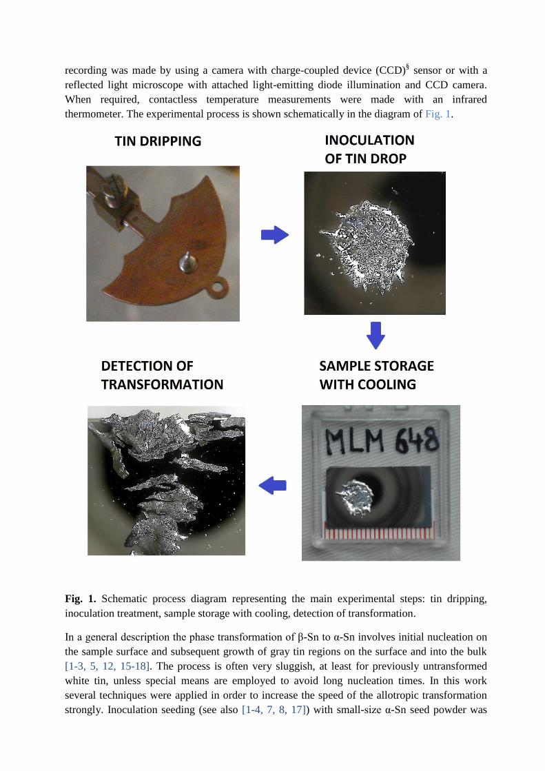
thermometer. The experimental process is shown schematically in the diagram of Fig. 1.
Fig. 1. Schematic process diagram representing the main experimental steps: tin dripping,
inoculation treatment, sample storage with cooling, detection of transformation.
In a general description the phase transformation of β-Sn to α-Sn involves initial nucleation on
the sample surface and subsequent growth of gray tin regions on the surface and into the bulk
[1-3, 5, 12, 15-18]. The process is often very sluggish, at least for previously untransformed
white tin, unless special means are employed to avoid long nucleation times. In this work
several techniques were applied in order to increase the speed of the allotropic transformation
strongly. Inoculation seeding (see also [1-4, 7, 8, 17]) with small-size α-Sn seed powder was
generally used for initiation of the autocatalytic conversion at several locations on the sample
surface. Seed powders of small grain size α-Sn were produced in a porcelain jar by several
successive transformations between the beta and alpha phase of tin by repeatedly cycling with
alternating prolonged cooling (to -24 °C) and short heating (to above 60 °C). Seeds were very
gently pressed in or just put in surface contact with the tin drop using clean plastic tweezers.
Inoculation with small pieces of isomorphic crystals from a high-purity CdTe wafer and with
fine Ge powder (99.999% purity) as foreign seeds [1, 3, 4, 8] was initially also tried but did not
yield any faster nucleation rates compared to what was obtained with α-Sn seeds; this method
was therefore no longer pursued. The ~1nm-thick thin oxide layer (SnO2) that develops on tin
surfaces during prolonged exposure to air [33] can prevent direct epitaxial contact with the seed
crystals. Consequently, drops were often (but not always) dipped in <24% concentrated HCl
(hydrochloric) acid solution for a few minutes, followed by brief rinsing in de-mineralized
water, in order to remove surface oxides before subsequent inoculation with seeds (see also [1-
8]). The polycrystalline material structure of the samples became apparent after removal of the
surface oxide layer by the acid.
It is known that prior mechanical deformation can increase the speed of α-Sn nucleation
substantially [1-8, 14, 17]. In particular, a pronounced increase was observed in studies where
less pure tin (~99.9%) was used [8, 13, 14, 16, 17]. The mechanism is attributed to lattice
distortions after deformation leading to increased dislocation density and stored internal strain
energy which can facilitate the allotropic β→α transition [3, 5, 8, 14, 17]. The transformation
speed can be increased significantly by prior cold-working even at room temperature although
recrystallization and recovery processes are then already expected to occur [3]. Specimen of
white tin with lower purity (types A, B and C) were deformed at temperatures of 17 °C - 19 °C
to reach a typical thickness reduction of 50% or more. For mechanical deformation the samples
were wrapped in Al foil and rolled out using a stainless steel rod for pressing.
For testing of EUV optics small rectangular and square pieces of Si (100) wafers (up to 1” size)
with the surface polished to <0.2 nm rms roughness were used. They were multilayer-coated by
electron-beam evaporation, deposited at Bielefeld University [34], and magnetron sputtering,
deposited by optiX fab [35], respectively. The MLMs consisted of uncapped Mo/Si multilayers
(50 bilayers) optimized for a peak reflectance Rmax above 0.65 at 13.5 nm at near normal
incidence. For exposure to tin dripping they were placed at 30 cm distance on the metal plate
below the heated Cu drip plate. The EUV reflectance of a sample from optiX fab was measured
at PTB Berlin in a reflectometer using synchrotron radiation [36].
3. Results and discussions
A consistent uniform interpretation of tin pest transformation based on results of past studies
for pure tin [2-4, 6, 7] and tin alloys [5, 8, 12-18] is difficult to obtain due to large variations of
the different individual test conditions. Therefore, in order to reach a better understanding of
the requirements for fast induction of tin pest, isolated tin drops were studied first without a
substrate. Initially, tests were carried out with β-Sn type A (99.9% purity grade) using surface
inoculation with α-Sn seed particles. However, no phase transformation could be induced in
reasonable time (on the order of several weeks) on untreated tin drops cooled at temperatures of
-24 °C even when the seeds were pressed into the specimen. On the other hand, when in
addition mechanical deformation with ~50% thickness reduction and surface oxide removal
with HCl was applied prior to inoculation with α-Sn seeds, the onset of tin pest growth in small
regions could be observed just within several days after sample storage at -24 °C by the change
from shiny metallic to dull gray color. Full completion of the transformation across the surface
of the drop required a considerably longer time. A similar behavior was found during use of tin
drops of Sn type B with same purity grade, but obtained from a different supplier (see Table 1).
These results with slow transformation induced by the combined use of seeding, mechanical
deformation and surface oxide removal are comparable to the recent observations reported by
Skwarek et al. for the case of alloys of 99% Sn with 1% Cu using tin of similar purity level [8].
For tin drops of higher purity grade 99.99% (Sn type C) the start of tin pest could be induced
after several days of cooling even when no prior deformation was made. Fig. 2 shows the
general development of the phase transformation observed on a representative typical tin drop
sample using Sn type C. The surface of the tin drop was treated with HCl and then inoculated
with a number of α-Sn seed particles mainly to the left of the central region (Fig. 2a). After 9
days storage at -24 °C gray tin blisters had spread in the infected region covering about 5% of
the total surface area, as shown in Fig. 2b. With continued cooling the regions of gray tin grew
further and merged. After 32 days of cooling nearly half of the surface area was transformed
(Fig. 2c). Due to large volume expansion the sample was also strongly deformed and a crack
started to open up at the center. The tin drop then began to disintegrate and broke up more and
more as the transformed surface area increased further (see Fig. 2d). When the sample was
fully converted it became very brittle and was easily broken into pieces, even when touched
only gently with plastic tweezers. Evidence of phase transformation is from the color change
from shiny silvery color to dull gray, from the observed deformation of the drop due to strong
volume expansion, and from the transition from ductile to highly brittle material behavior
revealing the structural change.
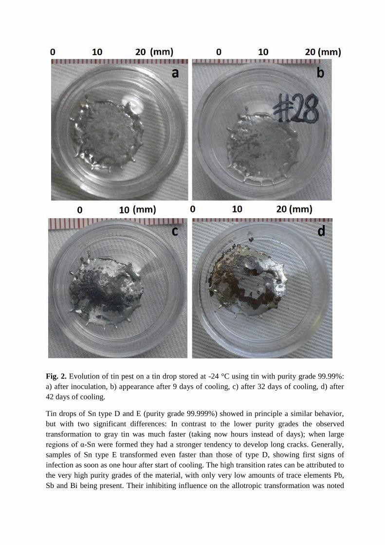
Fig. 2. Evolution of tin pest on a tin drop stored at -24 °C using tin with purity grade 99.99%:
a) after inoculation, b) appearance after 9 days of cooling, c) after 32 days of cooling, d) after
42 days of cooling.
Tin drops of Sn type D and E (purity grade 99.999%) showed in principle a similar behavior,
but with two significant differences: In contrast to the lower purity grades the observed
transformation to gray tin was much faster (taking now hours instead of days); when large
regions of α-Sn were formed they had a stronger tendency to develop long cracks. Generally,
samples of Sn type E transformed even faster than those of type D, showing first signs of
infection as soon as one hour after start of cooling. The high transition rates can be attributed to
the very high purity grades of the material, with only very low amounts of trace elements Pb,
Sb and Bi being present. Their inhibiting influence on the allotropic transformation was noted
in previous studies [1, 12-16]. As described in Sec. 2, Sn type E is expected to have even lower
levels of impurities compared to type D.
Inoculation by contacting the surface with seed particles was found to be a prerequisite for
initiation of nucleation of α-Sn on all tin drops examined here. As discussed by Styrkas [4], in
principle other mechanisms can also stimulate the nucleation of α-Sn on previously not
converted β-Sn samples, but generally they require considerably longer initiation times. It was
found here that prior deformation and even surface oxide removal was not an essential
ingredient for fast transformation (on the order of 24 hours) of drops with a tin purity grade of
99.999%. Even when seeds of α-Sn were just put in contact with the surface of the tin drop, a
full conversion to gray tin could typically be achieved in less than 12 hours for Sn type E, and
within at most 22 hours for Sn type D. When the surface oxides were removed in addition by
dipping in HCl acid, samples of β-Sn of type E showed generally a full conversion to gray tin
in less than 8 hours. Similarly fast transformation times were recently reported by Ref. [7] for
specimen with comparably high degree of tin purity.
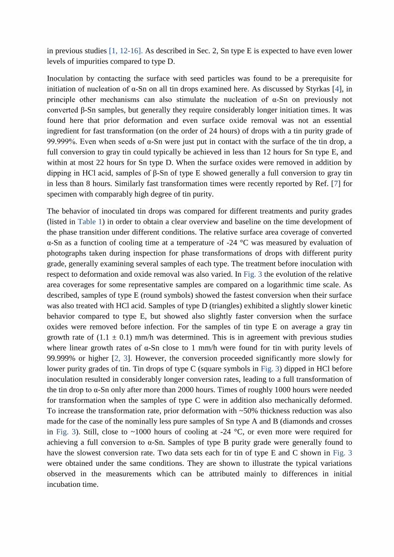
The behavior of inoculated tin drops was compared for different treatments and purity grades
(listed in Table 1) in order to obtain a clear overview and baseline on the time development of
the phase transition under different conditions. The relative surface area coverage of converted
α-Sn as a function of cooling time at a temperature of -24 °C was measured by evaluation of
photographs taken during inspection for phase transformations of drops with different purity
grade, generally examining several samples of each type. The treatment before inoculation with
respect to deformation and oxide removal was also varied. In Fig. 3 the evolution of the relative
area coverages for some representative samples are compared on a logarithmic time scale. As
described, samples of type E (round symbols) showed the fastest conversion when their surface
was also treated with HCl acid. Samples of type D (triangles) exhibited a slightly slower kinetic
behavior compared to type E, but showed also slightly faster conversion when the surface
oxides were removed before infection. For the samples of tin type E on average a gray tin
growth rate of (1.1 ± 0.1) mm/h was determined. This is in agreement with previous studies
where linear growth rates of α-Sn close to 1 mm/h were found for tin with purity levels of
99.999% or higher [2, 3]. However, the conversion proceeded significantly more slowly for
lower purity grades of tin. Tin drops of type C (square symbols in Fig. 3) dipped in HCl before
inoculation resulted in considerably longer conversion rates, leading to a full transformation of
the tin drop to α-Sn only after more than 2000 hours. Times of roughly 1000 hours were needed
for transformation when the samples of type C were in addition also mechanically deformed.
To increase the transformation rate, prior deformation with ~50% thickness reduction was also
made for the case of the nominally less pure samples of Sn type A and B (diamonds and crosses
in Fig. 3). Still, close to ~1000 hours of cooling at -24 °C, or even more were required for
achieving a full conversion to α-Sn. Samples of type B purity grade were generally found to
have the slowest conversion rate. Two data sets each for tin of type E and C shown in Fig. 3
were obtained under the same conditions. They are shown to illustrate the typical variations
observed in the measurements which can be attributed mainly to differences in initial
incubation time.
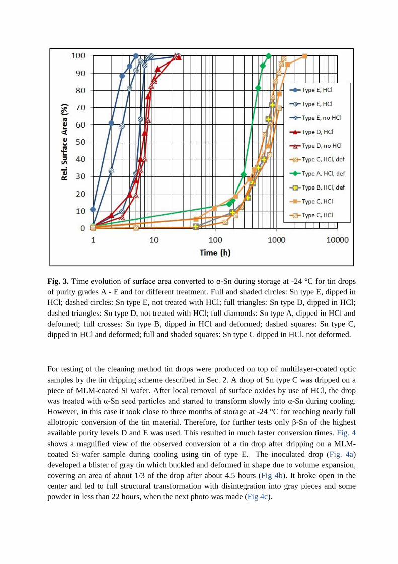
Fig. 3. Time evolution of surface area converted to α-Sn during storage at -24 °C for tin drops
of purity grades A - E and for different treatment. Full and shaded circles: Sn type E, dipped in
HCl; dashed circles: Sn type E, not treated with HCl; full triangles: Sn type D, dipped in HCl;
dashed triangles: Sn type D, not treated with HCl; full diamonds: Sn type A, dipped in HCl and
deformed; full crosses: Sn type B, dipped in HCl and deformed; dashed squares: Sn type C,
dipped in HCl and deformed; full and shaded squares: Sn type C dipped in HCl, not deformed.
For testing of the cleaning method tin drops were produced on top of multilayer-coated optic
samples by the tin dripping scheme described in Sec. 2. A drop of Sn type C was dripped on a
piece of MLM-coated Si wafer. After local removal of surface oxides by use of HCl, the drop
was treated with α-Sn seed particles and started to transform slowly into α-Sn during cooling.
However, in this case it took close to three months of storage at -24 °C for reaching nearly full
allotropic conversion of the tin material. Therefore, for further tests only β-Sn of the highest
available purity levels D and E was used. This resulted in much faster conversion times. Fig. 4
shows a magnified view of the observed conversion of a tin drop after dripping on a MLM-
coated Si-wafer sample during cooling using tin of type E. The inoculated drop (Fig. 4a)
developed a blister of gray tin which buckled and deformed in shape due to volume expansion,
covering an area of about 1/3 of the drop after about 4.5 hours (Fig 4b). It broke open in the
center and led to full structural transformation with disintegration into gray pieces and some
powder in less than 22 hours, when the next photo was made (Fig 4c).
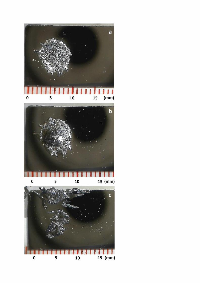
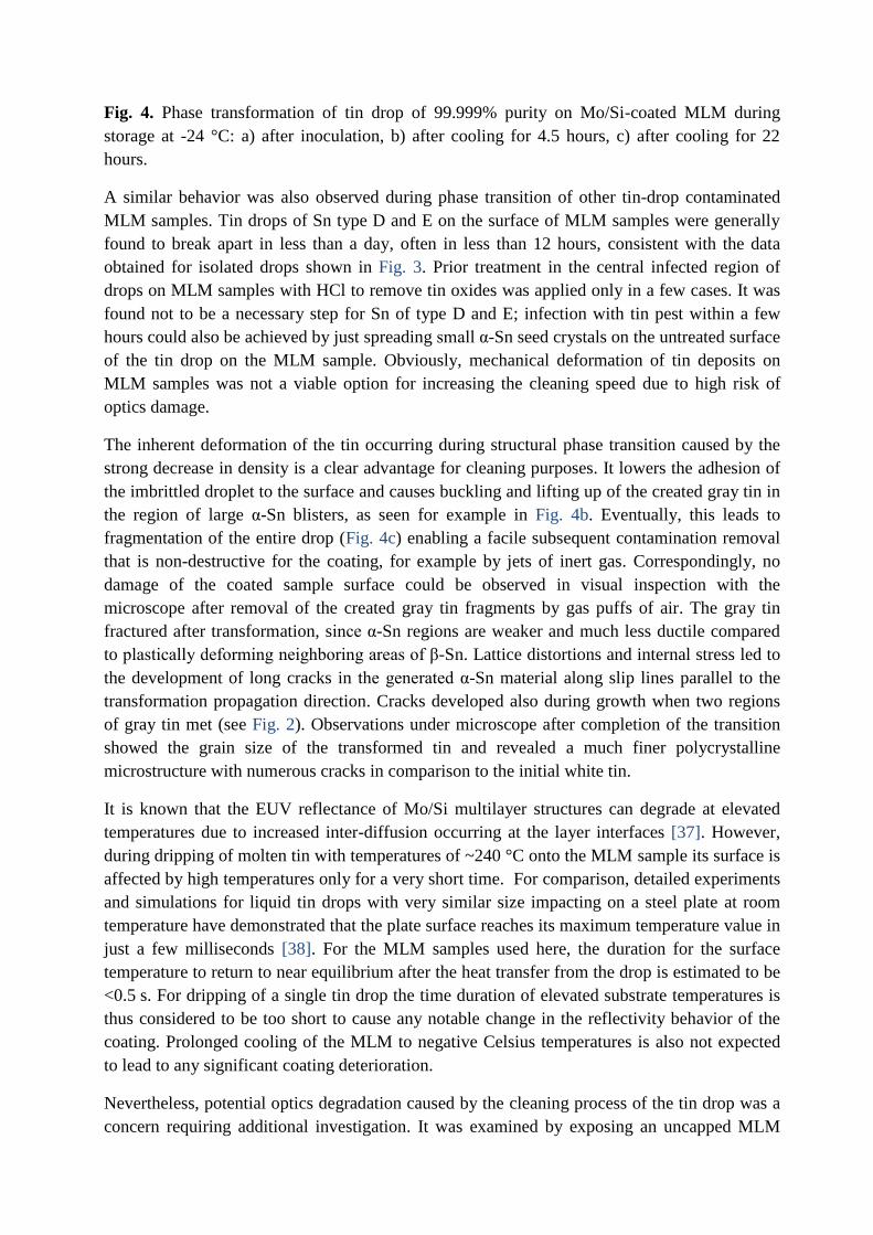
Fig. 4. Phase transformation of tin drop of 99.999% purity on Mo/Si-coated MLM during
storage at -24 °C: a) after inoculation, b) after cooling for 4.5 hours, c) after cooling for 22
hours.
A similar behavior was also observed during phase transition of other tin-drop contaminated
MLM samples. Tin drops of Sn type D and E on the surface of MLM samples were generally
found to break apart in less than a day, often in less than 12 hours, consistent with the data
obtained for isolated drops shown in Fig. 3. Prior treatment in the central infected region of
drops on MLM samples with HCl to remove tin oxides was applied only in a few cases. It was
found not to be a necessary step for Sn of type D and E; infection with tin pest within a few
hours could also be achieved by just spreading small α-Sn seed crystals on the untreated surface
of the tin drop on the MLM sample. Obviously, mechanical deformation of tin deposits on
MLM samples was not a viable option for increasing the cleaning speed due to high risk of
optics damage.
The inherent deformation of the tin occurring during structural phase transition caused by the
strong decrease in density is a clear advantage for cleaning purposes. It lowers the adhesion of
the imbrittled droplet to the surface and causes buckling and lifting up of the created gray tin in
the region of large α-Sn blisters, as seen for example in Fig. 4b. Eventually, this leads to
fragmentation of the entire drop (Fig. 4c) enabling a facile subsequent contamination removal
that is non-destructive for the coating, for example by jets of inert gas. Correspondingly, no
damage of the coated sample surface could be observed in visual inspection with the
microscope after removal of the created gray tin fragments by gas puffs of air. The gray tin
fractured after transformation, since α-Sn regions are weaker and much less ductile compared
to plastically deforming neighboring areas of β-Sn. Lattice distortions and internal stress led to
the development of long cracks in the generated α-Sn material along slip lines parallel to the
transformation propagation direction. Cracks developed also during growth when two regions
of gray tin met (see Fig. 2). Observations under microscope after completion of the transition
showed the grain size of the transformed tin and revealed a much finer polycrystalline
microstructure with numerous cracks in comparison to the initial white tin.
It is known that the EUV reflectance of Mo/Si multilayer structures can degrade at elevated
temperatures due to increased inter-diffusion occurring at the layer interfaces [37]. However,
during dripping of molten tin with temperatures of ~240 °C onto the MLM sample its surface is
affected by high temperatures only for a very short time. For comparison, detailed experiments
and simulations for liquid tin drops with very similar size impacting on a steel plate at room
temperature have demonstrated that the plate surface reaches its maximum temperature value in
just a few milliseconds [38]. For the MLM samples used here, the duration for the surface
temperature to return to near equilibrium after the heat transfer from the drop is estimated to be
<0.5 s. For dripping of a single tin drop the time duration of elevated substrate temperatures is
thus considered to be too short to cause any notable change in the reflectivity behavior of the
coating. Prolonged cooling of the MLM to negative Celsius temperatures is also not expected
to lead to any significant coating deterioration.
Nevertheless, potential optics degradation caused by the cleaning process of the tin drop was a
concern requiring additional investigation. It was examined by exposing an uncapped MLM
sample with previously measured EUV reflectance to the sequence of tin dripping, seed particle
inoculation and β → α transformation at -24 °C, followed by removal of the converted gray tin.
In this test an inoculated drop of tin type E was converted to gray tin fragments in just 7 hours
after start of cooling. The EUV reflectance of the cleaned sample was then measured once
more. The initial peak reflectance of the MLM coating was Rmax = 68.0 % at a wavelength of
13.61 nm. Its peak reflectance after cleaning, as determined by measurements at the PTB
reflectometer [36], was Rmax = 67.0 % in the region covered by the tin drop, and in the range of
67.2 % - 67.7 % outside of it. No change in peak and center wavelength as well as half width
was observed within measurement accuracy, thus confirming that the dripping of hot tin and
the cleaning process by the phase transformation did not induce any significant damage in the
MLM coating.
4. Conclusions
The tests carried out in this study have revealed the conditions for induction of tin pest on
samples of smooth drops of β-Sn leading to their conversion into brittle pieces of α-Sn thus
making them accessible for optics cleaning. It was found that the degree of purity of the
material is an essential factor governing the speed of transformation of drops inoculated by
seed particles. Prior deformation in addition to surface oxide removal and inoculation with α-
Sn seeds was required for samples of tin purity grades lower than 99.99% in order to reach
reasonably fast induction times of the phase transition during cooling at -24 °C. In contrast, for
tin of 99.999% nominal purity, fast full structural phase transformation could be achieved in
less than 24 hours of cooling by using only inoculation with α-Sn seed particles.
In a severe contamination scenario, smooth tin drops on MLM-coated EUV optics samples
stored at -24 °C could be rendered cleanable in less than one day by disintegration initiated by
induction of tin pest. It was shown that the EUV reflectivity of the MLM did not degrade
substantially (at most by 1%) after tin drop transformation and removal. The basic concept of
ex-situ optics cleaning by tin pest induction was thus proven in this work. Further studies are
required to examine practicable possibilities of inducing the allotropic phase transition in the
context of tin contamination removal, eventually also with in-situ techniques, in order to
improve the light source availability in EUV lithography scanners. Specifically, the cleaning
process based on tin pest induction can be optimized for multilayer-coated EUV collector
modules and drive laser deflection mirrors.
5. Acknowledgements
ASML Netherlands B.V. is acknowledged for motivating this study. The experiments were
carried out at BökoTech. I am grateful to the molecular and surface physics group of U.
Heinzmann at Bielefeld University for general support. In particular, I thank Christian Meier
(Bielefeld University) for helpful discussions and many valuable suggestions. Special thanks
go to him and to Torsten Feigl (optiX fab) for kindly supplying MLM-coated EUV optics
samples. Frank Scholze and his group at PTB Berlin are thanked for carrying out EUV
reflectance measurements.
This research did not receive any specific grant from funding agencies in the public,
commercial, or not-for-profit sectors.
6. References
[1] G.A. Busch, A. Kern, Solid State Physics 11 (1960) 1 – 40.
[2] J.H. Becker, J. Appl. Phys. 29 (1958) 1110 – 1121.
[3] K. Löhberg, P. Presche, Z. Metallkunde 59 (1968) 74 – 81.
[4] A.D. Styrkas, Inorg. Mater. 39 (2003) 806 – 810.
[5] Y.J. Joo, T. Takemoto, Mater. Lett. 56 (2002) 793 – 796.
[6] A.D. Styrkas, Inorg. Mater. 39 (2003) 683 – 686.
[7] J.L. Zuo, A.P. Xian, 14th
Int. Conf. on Electron. Pack. Techn. (2013) 152 – 155.
[8] A. Skwarek, P. Zachariasz, J. Kulawik, K. Witek, Mater. Chem. Phys.166 (2015) 16 –
19.
[9] A.W. Ewald, Helv. Phys. Acta 41 (1968) 795 – 813.
[10] K. Ojima, Y. Taneda, J. Mater. Sci. Lett. 10 (1991) 529 – 531.
[11] A.A. Matvienko, A.A. Sidelnikov, J. Alloys Compd. 252 (1997) 172 – 178.
[12] W.J. Plumbridge, J. Electron. Mater. 37 (2008) 218 – 223.
[13] Y. Kariya, N. Williams, C. Gagg, W. J. Plumbridge, J. Mater. 53 (2001) 39 – 41.
[14] W.J. Plumbridge, J. Mater. Sci: Mater. Electron. 18 (2007) 307 – 318.
[15] D. Di Maio, C. P. Hunt, J. Electron. Mater. 38 (2009) 1874 – 1879.
[16] M. Leodolter-Dworak, I. Steffan, W.J. Plumbridge, H. Ipser, J. Electron. Mater. 39
(2010) 105 – 108.
[17] A. Skwarek, M. Sroda, M. Pluska, A. Czerwinski, J. Ratajczak, K. Witek, Solder. Surf.
Mt. Tech. 23 (2011) 184 – 190.
[18] G. Zeng, S.D. McDonald, K. Sweatman, K. Nogita, ICEP 2014 Proceedings TB2-1
(2014) 135 -139.
[19] M.M.J.W. van Herpen, D.J.W. Klunder, W.A. Soer, R. Moors, V. Banine, Chem.
Phys. Let. 484 (2010) 197 – 199.
[20] J.R. Sporre, D. Elg, D.N. Ruzic, S.N. Srivastava, I.V. Fomenkov, D.C. Brandt, Proc.
SPIE 8679 ( 2013) 86792H.
[21] N.R. Böwering et al., J. Micro/Nanolith. MEMS MOEMS 4 (2009) 041504.
[22] D.C. Brandt et al., Proc. SPIE 9048 (2014) 90480C.
[23] H. Mizoguchi et al., Proc. SPIE 9084 (2014) 90480D.
[24] I.V. Fomenkov, D.C. Brandt, N.R. Farrar, B. La Fontaine, N.R. Böwering, D.J. Brown,
A.I. Ershov, D.W. Myers, Proc. SPIE 8679 (2013) 86792I.
[25] N. Farrar, D. Brandt, N. Böwering, Laser Focus World 45(3) (2009).
[26] T. Feigl et al., Proc. SPIE 8322 (2012) 832217.
[27] D. Elg, J.R. Sporre, G.A. Panici, S.N. Srivastava, D.N. Ruzic, J. Vac. Sci. Technol. A
34 (2016) 021305.
[28] T. Feigl et al., Proc. SPIE 8679 (2013) 86790C.
[29] O.T. Ehrler, U. Meier, A. Uhl, H. Kierey, PCT application (2013) WO 2013/159928
A1.
[30] M. Becker, U. Müller, O. Arp, PCT application (2015) WO 2015/043833 A1.
[31] I. Varghese, C.W. Bowers, M. Balooch, Proc. SPIE 8166 (2011) 816615.
[32] Westfalenzinn, technical data sheet: tin anodes, http://www.westfalenzinn.de.
[33] S. Cho, J. Yu, S.K. Kang, D.Y. Shih, JOM 57 (2005) 50-52.
[34] U. Kleineberg, Th. Westerwalbesloh, W. Hachmann, U. Heinzmann, J. Tümmler, F.
Scholze, G. Ulm, S. Muellender, Thin Solid Films 433 (2003) 230 – 236.
[35] M. Perske, H. Pauer, T. Fiedler, S. Yulin, V. Nesterenko, M. Schürmann, T. Feigl, N.
Kaiser, “New high reflective multilayer designs for the EUV and soft X-ray range“,
Presentation at Int. Workshop on EUV Soft X-ray Sources (2012).
[36] C. Laubis et al., Proc. SPIE 8679 (2013) 867921.
[37] R.S. Rosen, M.A. Viliardos, M.E. Kassner, D.G. Stearns, S.P. Vernon, Proc. SPIE
1547 (1991) 212 – 220.
[38] M. Pasandideh-Fard, R. Bhola, S. Chandra, J. Mostaghimi, Int. J. Heat and Mass
Trans. 41 (1998) 2929-2945.

Top Related