

γλώσσες
Σελίδες
Νομικός

Exercises for Differential Amplifiers
ECE 102, Fall 2012, F. Najmabadi

F. Najmabadi, ECE102, Fall 2012 (2/37)
Exercise 1: Compute VD , VS , VDS and VGS if ID3 = 2 mA, RD = 500 Ω, VOV3 = 0.5 V, and identical Q1 &Q2 with µnCox (W/L ) = 8 mA/V2, Vt = 0.5 V, λ = 0. A) For VG = 0 and B) For VG = 1 V. Repeat the exercise for λ = 0.1 V-1.
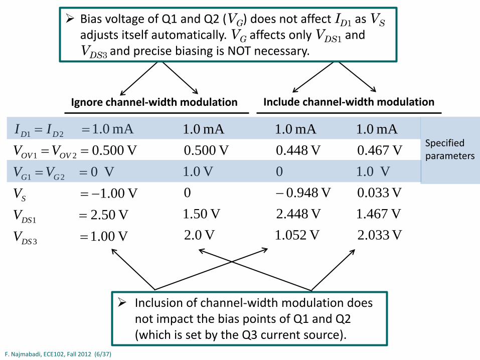
This exercise shows that precise biasing of Q1 and Q2 is not necessary as VS adjusts itself automatically.
Inclusion of channel-width modulation does not impact the bias points of Q1 and Q2 (which is set by the current source).
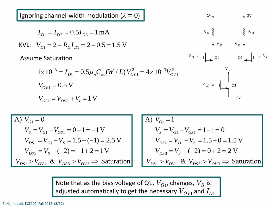
F. Najmabadi, ECE102, Fall 2012 (3/37)
Assume Saturation
V 111 =+= tOVGS VVV
Saturation & V 121)2(
V 5.2)1(5.1 V 110
0 A)
3311
3
11
11
1
⇒>>=+−=−−==−−=−=
−=−=−==
OVDSOVDS
SDS
SDDS
GSGS
G
VVVVVV
VVVVVV
V
V 5.01 =OVV
Ignoring channel-width modulation (λ = 0)
21
3211
3 104 )/(5.0101 OVOVoxnD VVLWCI −− ×===× µ
V 5.15.022 11 =−=−= DDD IRVKVL:
Note that as the bias voltage of Q1, VG1, changes, VS is adjusted automatically to get the necessary VOV1 and ID1
mA 15.0 321 === DDD III
Saturation & V 220)2(
V 5.105.1 011
1 A)
3311
3
11
11
1
⇒>>=+=−−==−=−=
=−=−==
OVDSOVDS
SDS
SDDS
GSGS
G
VVVVVV
VVVVVV
V
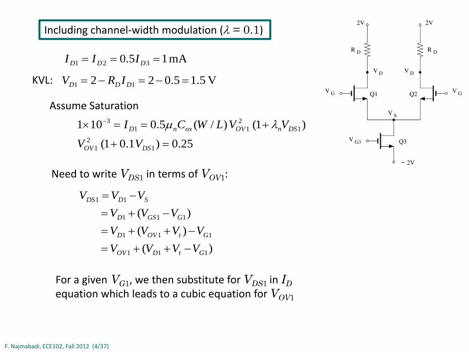
F. Najmabadi, ECE102, Fall 2012 (4/37)
Assume Saturation
)( )( )(
111
111
111
11
GtDOV
GtOVD
GGSD
SDDS
VVVVVVVV
VVVVVV
−++=−++=
−+=−=
Including channel-width modulation (λ = 0.1)
25.0) 1.01(
)1( )/(5.0101
12
1
12
113
=+
+==× −
DSOV
DSnOVoxnD
VVVVLWCI λµ
Need to write VDS1 in terms of VOV1:
For a given VG1, we then substitute for VDS1 in ID equation which leads to a cubic equation for VOV1
V 5.15.022 11 =−=−= DDD IRVKVL:
mA 15.0 321 === DDD III
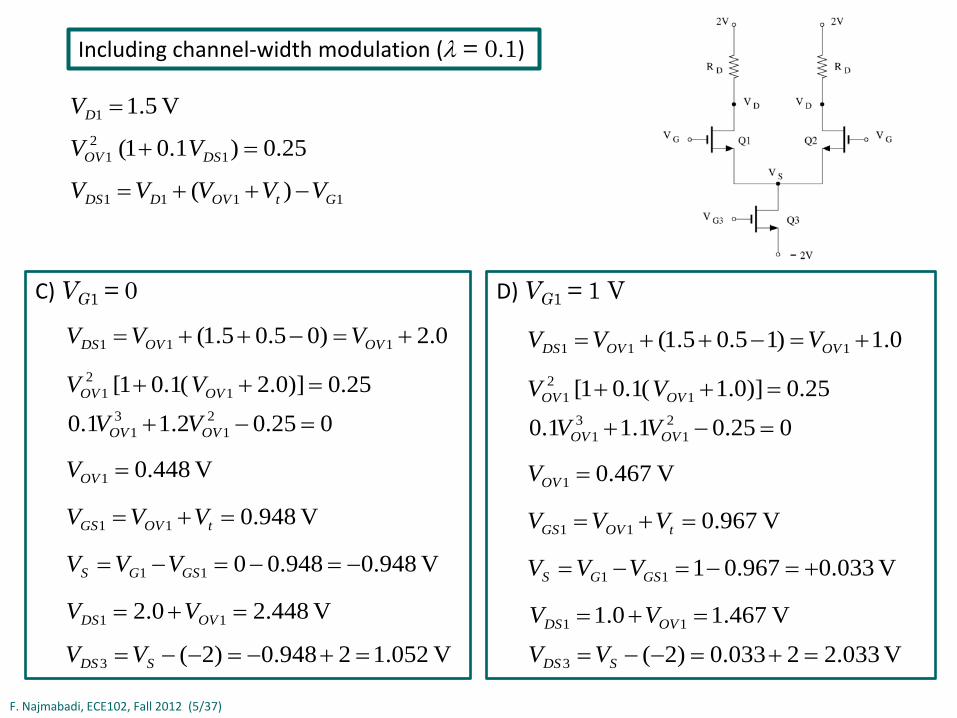
F. Najmabadi, ECE102, Fall 2012 (5/37)
V 948.011 =+= tOVGS VVV
1111 )( GtOVDDS VVVVV −++=
V 448.01 =OVV
Including channel-width modulation (λ = 0.1)
25.0) 1.01( 12
1 =+ DSOV VV
V 5.11 =DV
V 948.0948.0011 −=−=−= GSGS VVV
C) VG1 = 0
0.2)05.05.1( 111 +=−++= OVOVDS VVV
025.02.11.0
25.0)]0.2 (1.01[ 2
13
1
12
1
=−+
=++
OVOV
OVOV
VVVV
V 448.20.2 11 =+= OVDS VV
V 967.011 =+= tOVGS VVV
V 467.01 =OVV
V 033.0967.0111 +=−=−= GSGS VVV
0.1)15.05.1( 111 +=−++= OVOVDS VVV
025.01.11.0
25.0)]0.1 (1.01[ 2
13
1
12
1
=−+
=++
OVOV
OVOV
VVVV
V 467.10.1 11 =+= OVDS VV
D) VG1 = 1 V
V 052.12948.0)2(3 =+−=−−= SDS VV V 033.22033.0)2(3 =+=−−= SDS VV
F. Najmabadi, ECE102, Fall 2012 (6/37)
V 00.1 V 50.2
V 00.1 V 0
V 500.0 mA 0.1
3
1
21
21
21
==−=
======
DS
DS
S
GG
OVOV
DD
VVV
VVVV
II
Include channel-width modulation
Specified parameters
Inclusion of channel-width modulation does not impact the bias points of Q1 and Q2 (which is set by the Q3 current source).
V 2.0V 50.1
0V 0.1
V 500.0mA 0.1
V 1.052V 448.2
V 948.00
V 448.0mA 0.1
−
V 2.033V 467.1V 033.0
V 0.1V 467.0
mA 0.1
Ignore channel-width modulation
Bias voltage of Q1 and Q2 (VG) does not affect ID1 as VS adjusts itself automatically. VG affects only VDS1 and VDS3 and precise biasing is NOT necessary.
F. Najmabadi, ECE102, Fall 2012 (7/37)
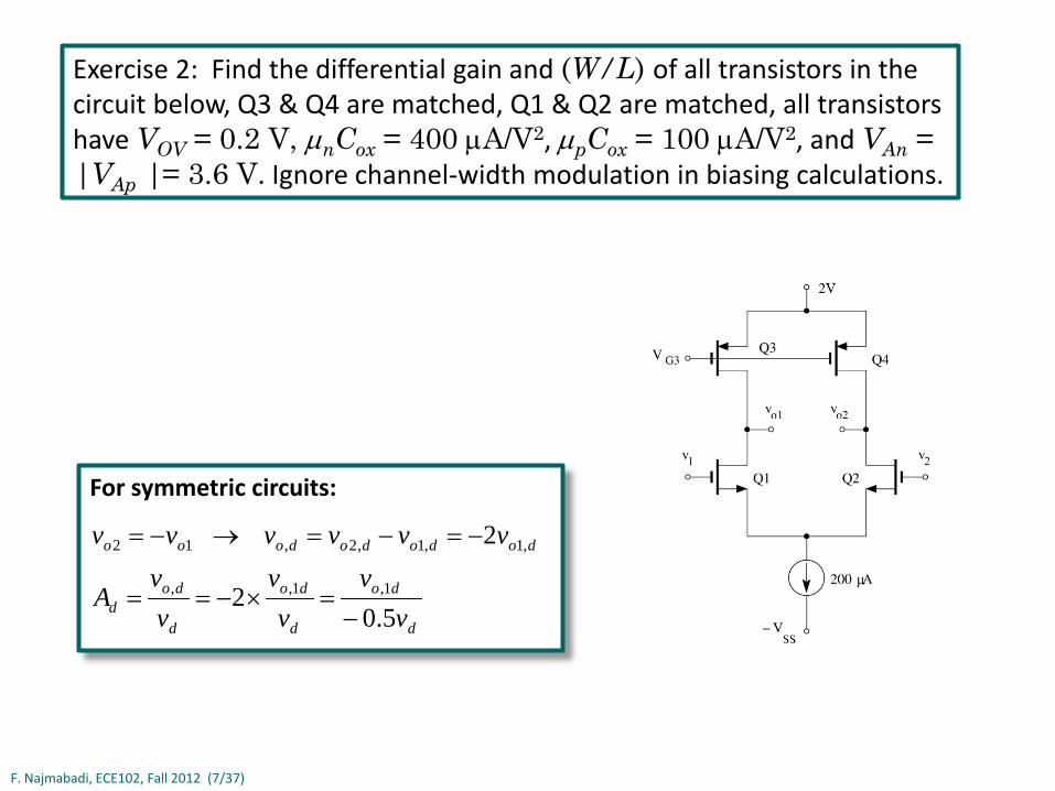
Exercise 2: Find the differential gain and (W/L) of all transistors in the circuit below, Q3 & Q4 are matched, Q1 & Q2 are matched, all transistors have VOV = 0.2 V, µnCox = 400 µA/V2, µpCox = 100 µA/V2, and VAn = |VAp |= 3.6 V. Ignore channel-width modulation in biasing calculations.
For symmetric circuits:
d
do
d
do
d
dod
dodododooo
vv
vv
vv
A
vvvvvv
5.02
2
1,1,,
,1,1,2,12
−=×−==
−=−=→−=

F. Najmabadi, ECE102, Fall 2012 (8/37)
Since transistors are matched and have the same VOV :
21
2111
6
)/(5.12)/( )/(5.010100
LWLWVLWCI OVoxnD
====× − µ
A 1004321 µ==== DDDD IIII
43
2333
6
)/(50)/(
)/(5.010100
LWLWVLWCI OVoxpD
==
==× − µ
A/V 102 3
1
11
−==OV
Dm V
Ig k 361
11 ==
D
Ao I
Vr
Differential Mode Half Circuit
k 363
33 ==
D
Ao I
Vr
18101810k) 36||k 36(10)||( 333o3o11 −=××−=−=−= --
md rrgA
)||( 5.0
311
1,,
oom
d
do
d
dod
rrgv
vvv
A
−=−
==
F. Najmabadi, ECE102, Fall 2012 (9/37)
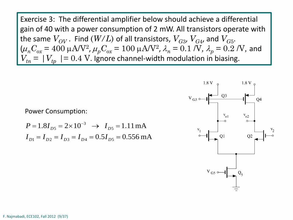
Exercise 3: The differential amplifier below should achieve a differential gain of 40 with a power consumption of 2 mW. All transistors operate with the same VOV . Find (W/L) of all transistors, VG3, VG4, and VG5. (µnCox = 400 µA/V2, µpCox = 100 µA/V2, λn = 0.1 /V, λp = 0.2 /V, and Vtn = |Vtp |= 0.4 V. Ignore channel-width modulation in biasing.
Power Consumption:
mA 556.05.0mA 11.1 1028.1
54321
53
5
======→×== −
DDDDD
DD
IIIIIIIP
F. Najmabadi, ECE102, Fall 2012 (10/37)
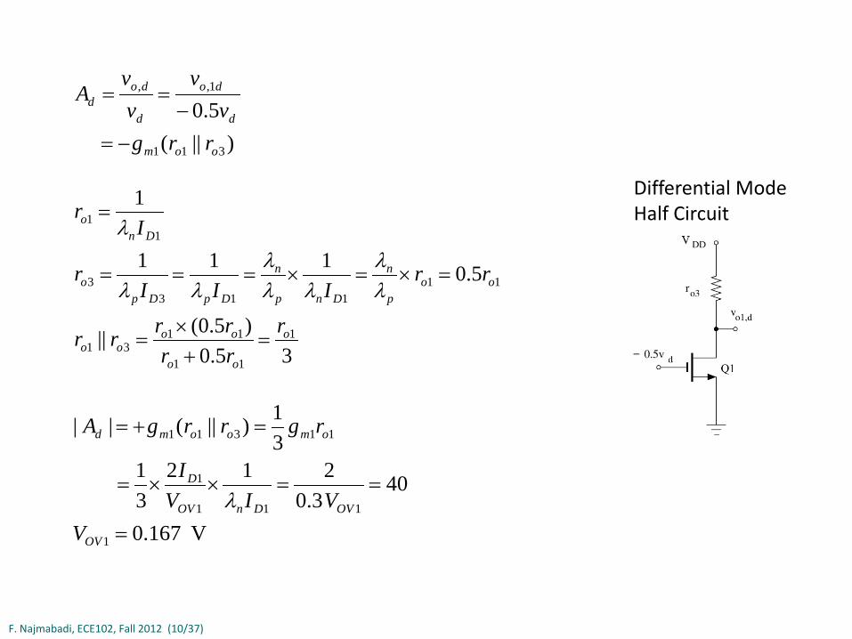
Differential Mode Half Circuit
35.0)5.0(||
5.011 1
1
1
11
1131
11113
3
11
o
oo
oooo
oop
n
Dnp
n
DpDpo
Dno
rrrrrrr
rrIII
r
Ir
=+×
=
=×=×===
=
λλ
λλλ
λλ
λ
V 167.0
40 3.0212
31
31)||( ||
1
111
1
11311
=
==××=
=+=
OV
OVDnOV
D
omoomd
VVIV
I
rgrrgA
λ
)||( 5.0
311
1,,
oom
d
do
d
dod
rrgv
vvv
A
−=−
==
F. Najmabadi, ECE102, Fall 2012 (11/37)
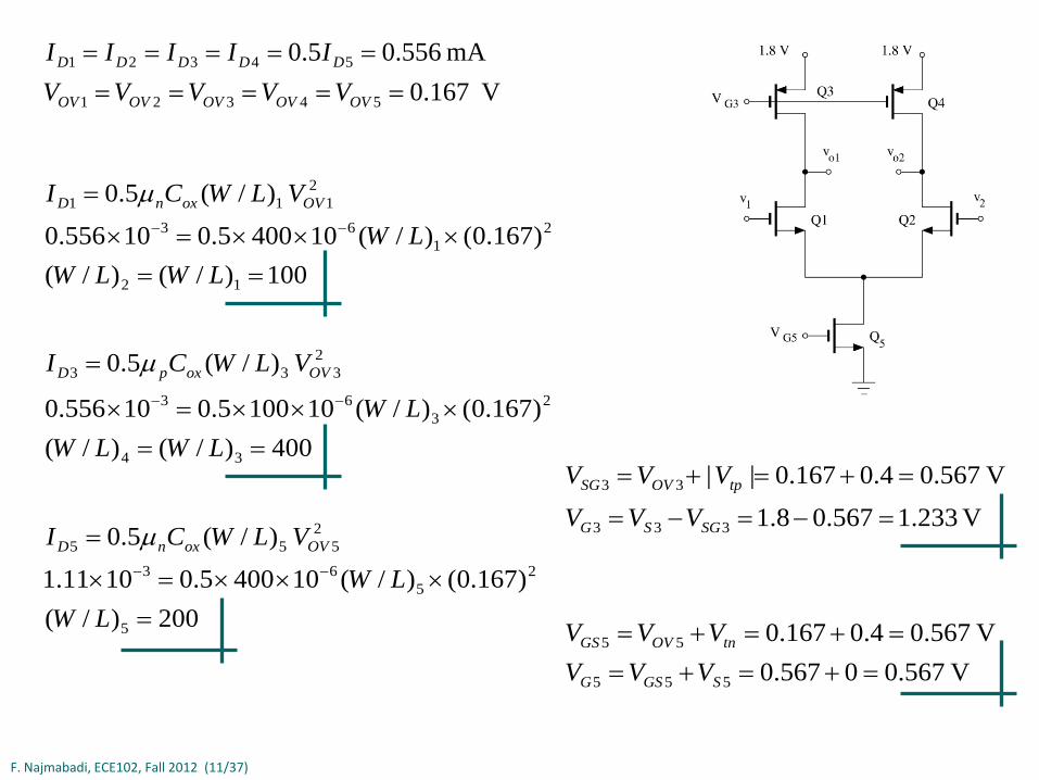
V 167.0mA 556.05.0
54321
54321
==========
OVOVOVOVOV
DDDDD
VVVVVIIIII
100)/()/()167.0()/(104005.010556.0
)/(5.0
12
21
63
2111
==×××=×
=−−
LWLWLW
VLWCI OVoxnD µ
400)/()/()167.0()/(101005.010556.0
)/(5.0
34
23
63
2333
==×××=×
=−−
LWLWLW
VLWCI OVoxpD µ
200)/()167.0()/(104005.01011.1
)/(5.0
5
25
63
2555
=×××=×
=−−
LWLW
VLWCI OVoxnD µ
V 567.00567.0V 567.04.0167.0
555
55
=+=+==+=+=
SGSG
tnOVGS
VVVVVV
V 233.1567.08.1
V 567.04.0167.0||
333
33
=−=−=
=+=+=
SGSG
tpOVSG
VVVVVV
F. Najmabadi, ECE102, Fall 2012 (12/37)
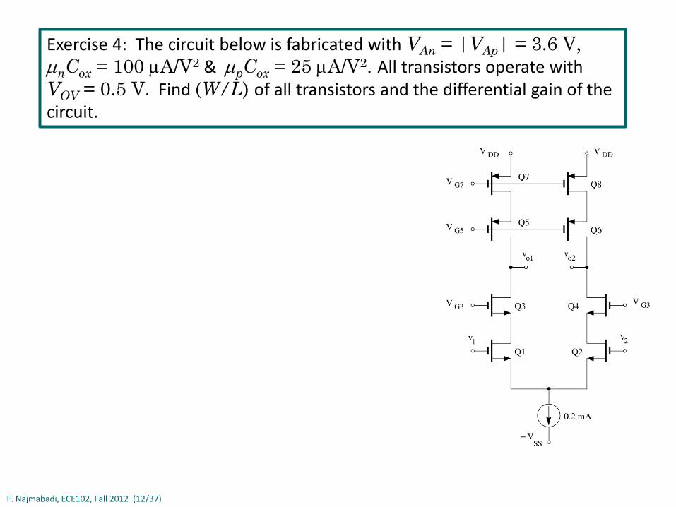
Exercise 4: The circuit below is fabricated with VAn = |VAp| = 3.6 V, µnCox = 100 µA/V2 & µpCox = 25 µA/V2. All transistors operate with VOV = 0.5 V. Find (W/L) of all transistors and the differential gain of the circuit.
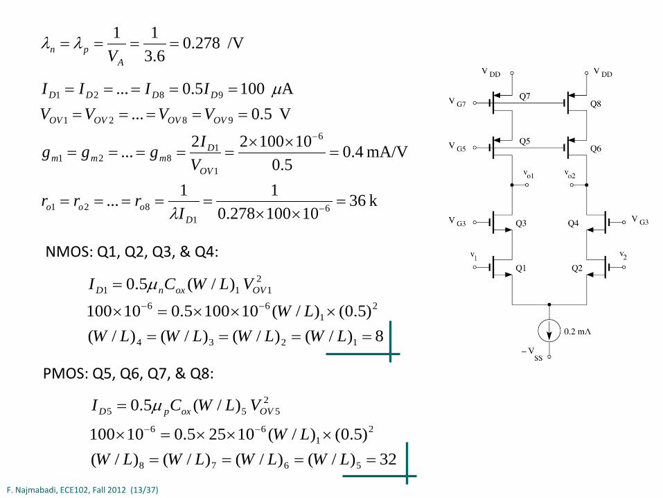
F. Najmabadi, ECE102, Fall 2012 (13/37)
k 3610100278.0
11...
mA/V 4.05.0
1010022...
V 5.0...A 1005.0...
61
821
6
1
1821
9821
9821
=××
=====
=××
=====
==========
−
−
Dooo
OV
Dmmm
OVOVOVOV
DDDD
Irrr
VIggg
VVVVIIII
λ
µ
/V0.2786.3
11====
Apn V
λλ
NMOS: Q1, Q2, Q3, & Q4:
8)/()/()/()/()5.0()/(101005.010100
)/(5.0
1234
21
66
2111
====×××=×
=−−
LWLWLWLWLW
VLWCI OVoxnD µ
PMOS: Q5, Q6, Q7, & Q8:
32)/()/()/()/()5.0()/(10255.010100
)/(5.0
5678
21
66
2555
====×××=×
=−−
LWLWLWLWLW
VLWCI OVoxpD µ
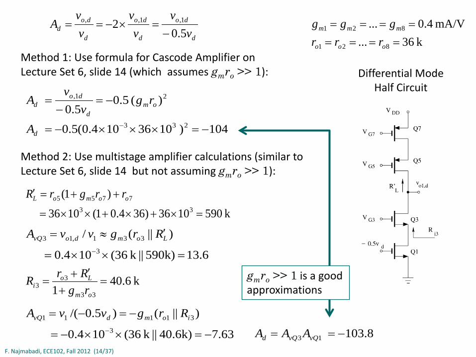
F. Najmabadi, ECE102, Fall 2012 (14/37)
Differential Mode Half Circuit
7.6340.6k)||k 36(100.4
)||()5.0/(3
31111
−=××−=
−=−=−
iomdvQ RrgvvA
k 6.401
33
33 =
+′+
=om
Loi rg
RrR
8.103 13 −== vQvQd AAA
k 36...mA/V 4.0...
821
821
========
ooo
mmm
rrrggg
k 5901036)364.01(1036
)1(33
7755
=×+×+××=
++=′ oomoL rrgrR
Method 1: Use formula for Cascode Amplifier on Lecture Set 6, slide 14 (which assumes gmro >> 1):
104) 1036100.4(5.0
)( 5.05.0
233
21,
−=×××−=
−=−
=
−d
omd
dod
A
rgv
vA
d
do
d
do
d
dod v
vv
vvv
A5.0
2 1,1,,
−=×−==
Method 2: Use multistage amplifier calculations (similar to Lecture Set 6, slide 14 but not assuming gmro >> 1):
13.6590k)||k 36(100.4
)||(/3
331,13
=××=
′≈=−
LomdovQ RrgvvA
gmro >> 1 is a good approximations
F. Najmabadi, ECE102, Fall 2012 (15/37)
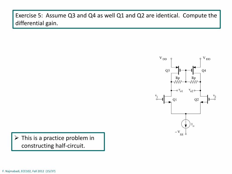
Exercise 5: Assume Q3 and Q4 as well Q1 and Q2 are identical. Compute the differential gain.
This is a practice problem in constructing half-circuit.
F. Najmabadi, ECE102, Fall 2012 (16/37)
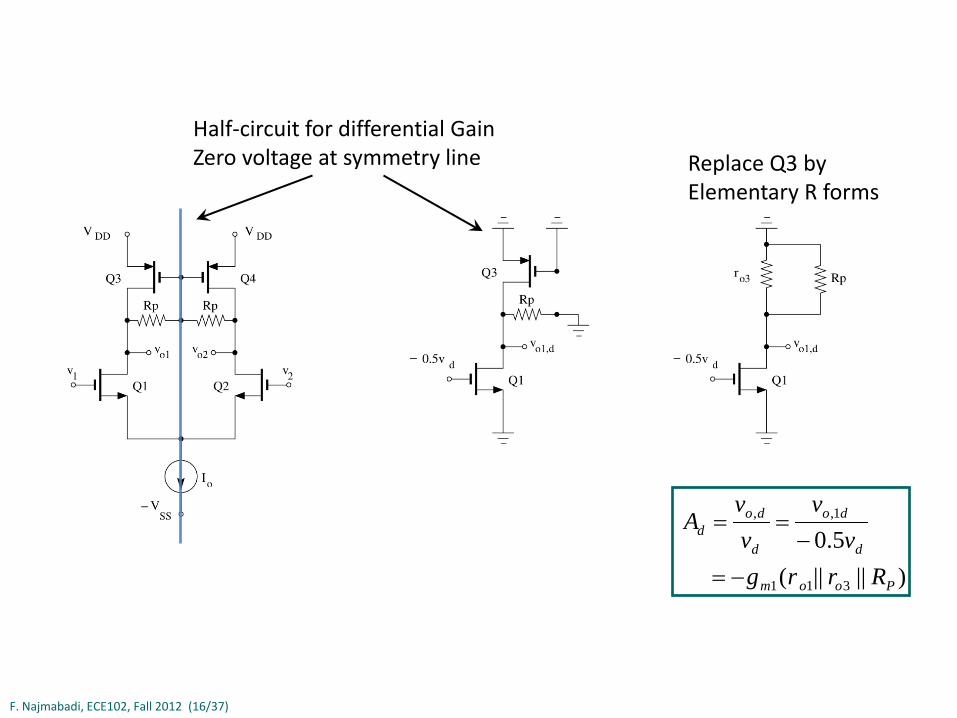
Half-circuit for differential Gain Zero voltage at symmetry line Replace Q3 by
Elementary R forms
)||||(
5.0
311
1,,
Poom
d
do
d
dod
Rrrgv
vvv
A
−=−
==
F. Najmabadi, ECE102, Fall 2012 (17/37)
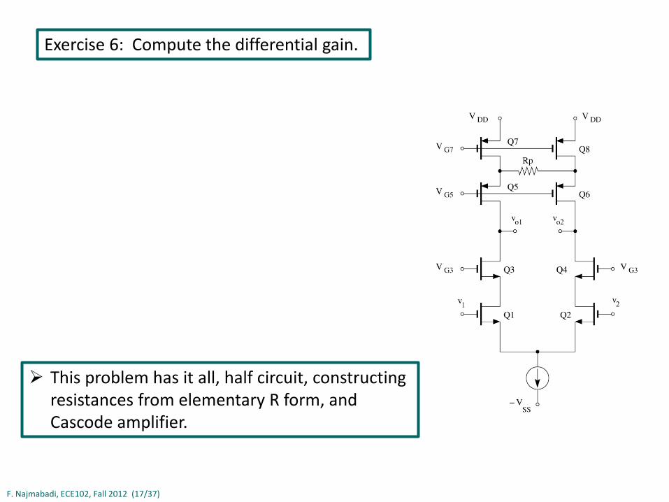
Exercise 6: Compute the differential gain.
This problem has it all, half circuit, constructing resistances from elementary R form, and Cascode amplifier.
F. Najmabadi, ECE102, Fall 2012 (18/37)
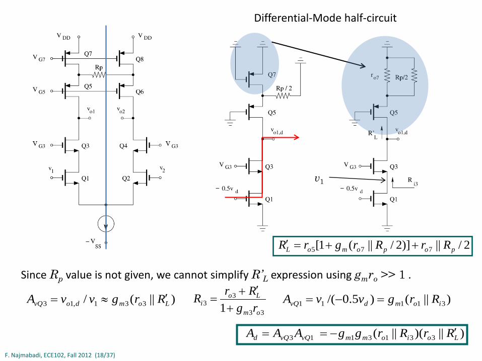
Differential-Mode half-circuit
2/|| )]2/||(1[ 775 popomoL RrRrgrR ++=′
)||()5.0/( 31111 iomdvQ RrgvvA =−=33
33 1
om
Loi rg
RrR+
′+=
)||)(||( 3313113 LoiommvQvQd RrRrggAAA ′−==
)||(/ 331,13 LomdovQ RrgvvA ′≈=
Since Rp value is not given, we cannot simplify R’L expression using gmro >> 1 .
v1
F. Najmabadi, ECE102, Fall 2012 (19/37)
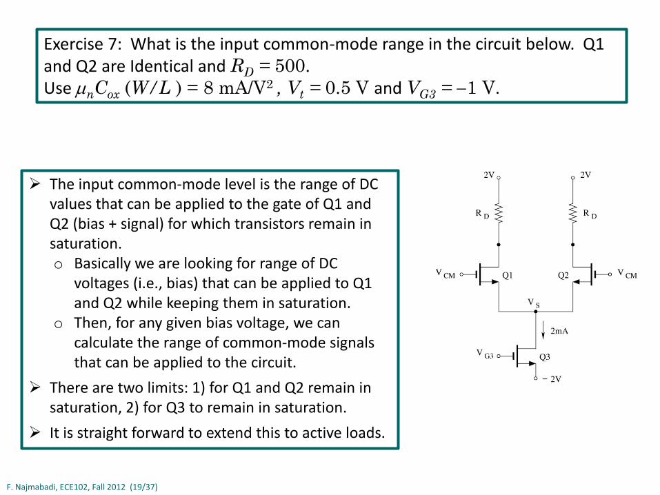
Exercise 7: What is the input common-mode range in the circuit below. Q1 and Q2 are Identical and RD = 500. Use µnCox (W/L ) = 8 mA/V2 , Vt = 0.5 V and VG3 = −1 V.
The input common-mode level is the range of DC values that can be applied to the gate of Q1 and Q2 (bias + signal) for which transistors remain in saturation. o Basically we are looking for range of DC
voltages (i.e., bias) that can be applied to Q1 and Q2 while keeping them in saturation.
o Then, for any given bias voltage, we can calculate the range of common-mode signals that can be applied to the circuit.
There are two limits: 1) for Q1 and Q2 remain in saturation, 2) for Q3 to remain in saturation.
It is straight forward to extend this to active loads.
F. Najmabadi, ECE102, Fall 2012 (20/37)
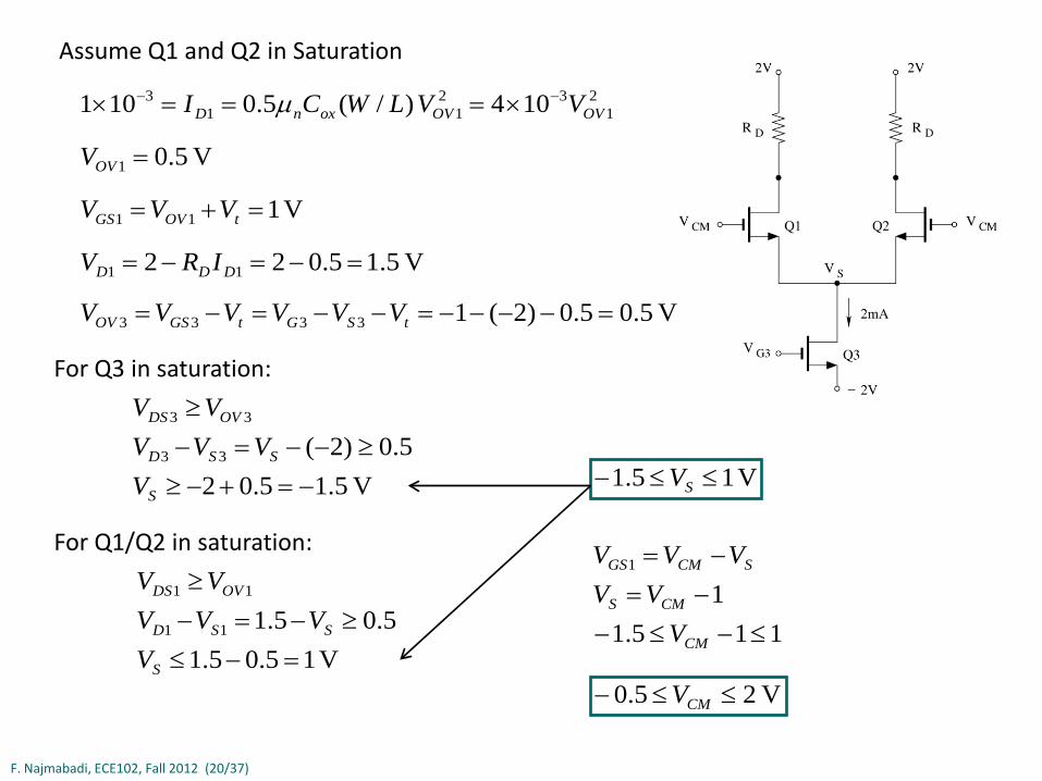
Assume Q1 and Q2 in Saturation
21
3211
3 104 )/(5.0101 OVOVoxnD VVLWCI −− ×===× µ
V 111 =+= tOVGS VVV
V 5.15.022 11 =−=−= DDD IRV
V 5.01 =OVV
115.11
1
≤−≤−−=−=
CM
CMS
SCMGS
VVV
VVV
V 15.1 ≤≤− SVV 5.15.025.0)2(33
33
−=+−≥≥−−=−
≥
S
SSD
OVDS
VVVV
VVFor Q3 in saturation:
V 5.05.0)2(13333 =−−−−=−−=−= tSGtGSOV VVVVVV
For Q1/Q2 in saturation:
V 15.05.15.05.111
11
=−≤≥−=−
≥
S
SSD
OVDS
VVVV
VV
V 25.0 ≤≤− CMV
F. Najmabadi, ECE102, Fall 2012 (21/37)
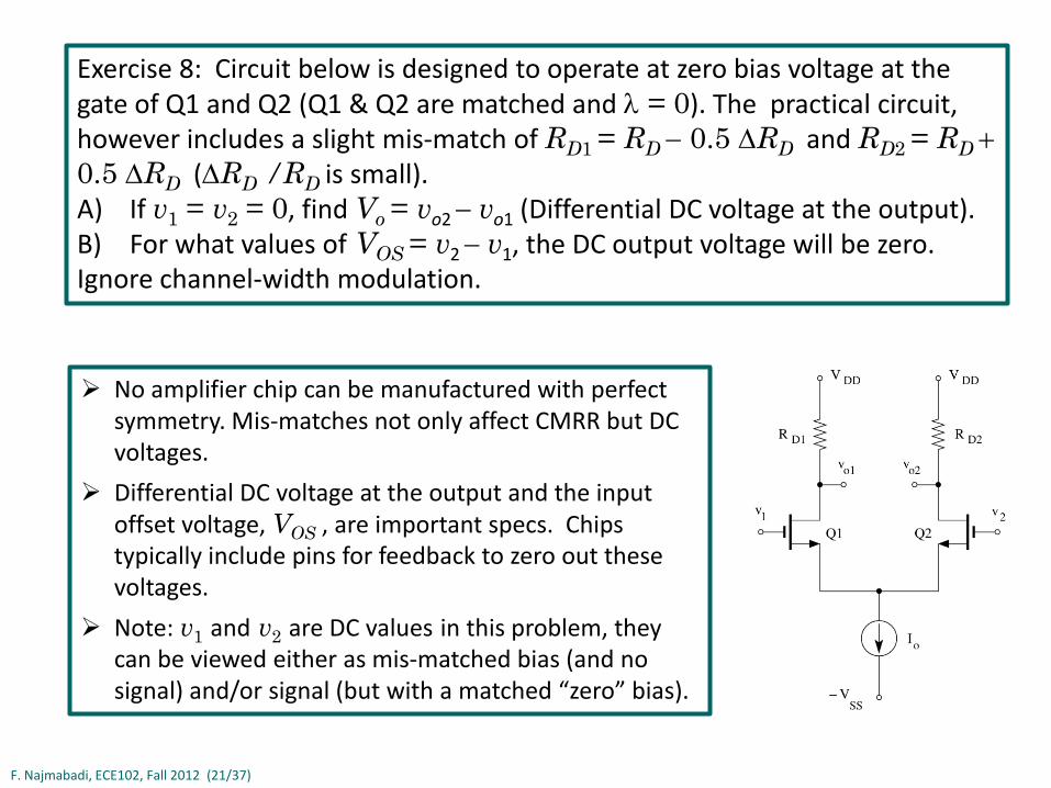
Exercise 8: Circuit below is designed to operate at zero bias voltage at the gate of Q1 and Q2 (Q1 & Q2 are matched and λ = 0). The practical circuit, however includes a slight mis-match of RD1 = RD − 0.5 ∆RD and RD2 = RD + 0.5 ∆RD (∆RD /RD is small). A) If v1 = v2 = 0, find Vo = vo2 − vo1 (Differential DC voltage at the output). B) For what values of VOS = v2 − v1, the DC output voltage will be zero. Ignore channel-width modulation.
No amplifier chip can be manufactured with perfect symmetry. Mis-matches not only affect CMRR but DC voltages.
Differential DC voltage at the output and the input offset voltage, VOS , are important specs. Chips typically include pins for feedback to zero out these voltages.
Note: v1 and v2 are DC values in this problem, they can be viewed either as mis-matched bias (and no signal) and/or signal (but with a matched “zero” bias).
F. Najmabadi, ECE102, Fall 2012 (22/37)
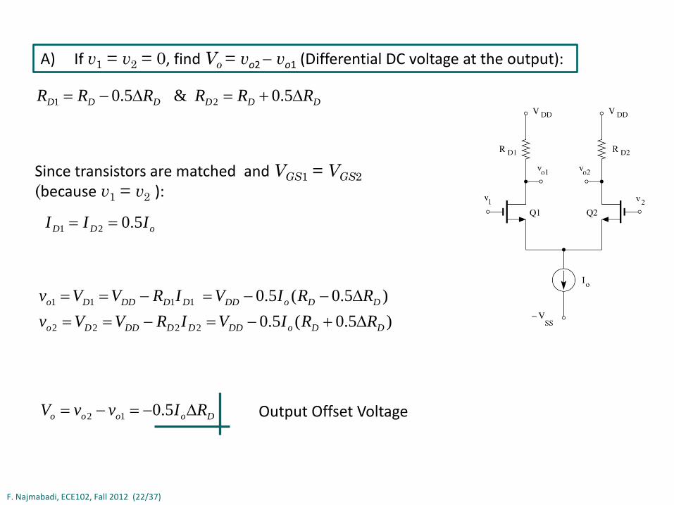
Since transistors are matched and VGS1 = VGS2 (because v1 = v2 ):
)5.0(5.0)5.0(5.0
2222
1111
DDoDDDDDDDo
DDoDDDDDDDo
RRIVIRVVvRRIVIRVVv∆+−=−==∆−−=−==
oDD III 5.021 ==
Doooo RIvvV ∆−=−= 5.012 Output Offset Voltage
A) If v1 = v2 = 0, find Vo = vo2 − vo1 (Differential DC voltage at the output):
DDDDDD RRRRRR ∆+=∆−= 5.0 & 5.0 21
F. Najmabadi, ECE102, Fall 2012 (23/37)
oDD III 5.021 ==
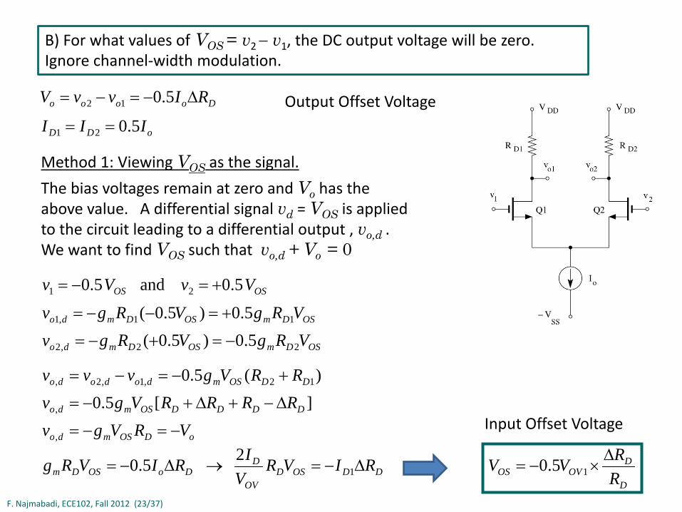
Method 1: Viewing VOS as the signal.
The bias voltages remain at zero and Vo has the above value. A differential signal vd = VOS is applied to the circuit leading to a differential output , vo,d . We want to find VOS such that vo,d + Vo = 0
Doooo RIvvV ∆−=−= 5.012 Output Offset Voltage
oDOSmdo
DDDDOSmdo
DDOSmdododo
VRVgvRRRRVgvRRVgvvv
−=−=
∆−+∆+−=
+−=−=
,
,
12,1,2,
][5.0)(5.0
DDOSDOV
DDoOSDm RIVR
VIRIVRg ∆−=→∆−= 1
2 5.0 5.0 1D
DOVOS R
RVV ∆×−=
OSOS VvVv 5.0 and 5.0 21 +=−=
Input Offset Voltage
B) For what values of VOS = v2 − v1, the DC output voltage will be zero. Ignore channel-width modulation.
OSDmOSDmdo
OSDmOSDmdo
VRgVRgvVRgVRgv
22,2
11,1
5.0)5.0(5.0)5.0(
−=+−=
+=−−=
F. Najmabadi, ECE102, Fall 2012 (24/37)
221121 DDDDDDDDoo IRVIRVvv −=−→=
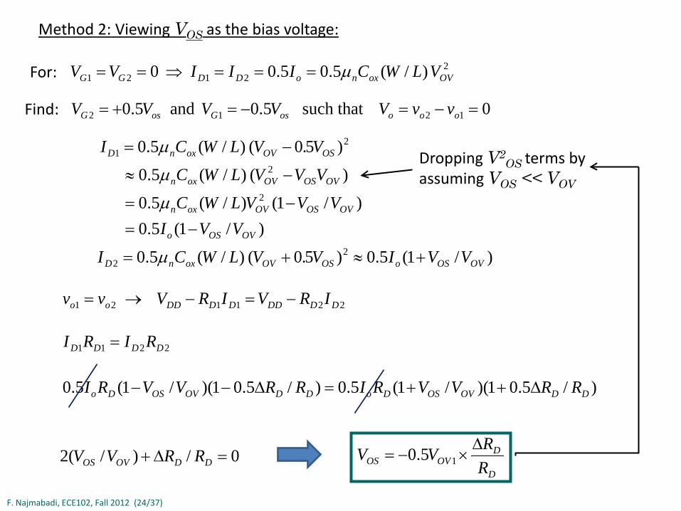
Method 2: Viewing VOS as the bias voltage:
0 such that 5.0 and 5.0 1212 =−=−=+= oooosGosG vvVVVVV
)/(5.05.0 0 22121 OVoxnoDDGG VLWCIIIVV µ===⇒==
)/1(5.0 )/1()/(5.0
)( )/(5.0
)50( )/(5.0
2
2
21
OVOSo
OVOSOVoxn
OVOSOVoxn
OSOVoxnD
VVIVVVLWC
VVVLWCV.VLWCI
−=−=
−≈
−=
µ
µ
µ
)/1(5.0)50( )/(5.0 22 OVOSoOSOVoxnD VVIV.VLWCI +≈+= µ
0/)/(2 =∆+ DDOVOS RRVV
)/5.01)(/1(5.0)/5.01)(/1(5.0 DDOVOSDoDDOVOSDo RRVVRIRRVVRI ∆++=∆−−
For:
Find:
5.0 1D
DOVOS R
RVV ∆×−=
2211 DDDD RIRI =
Dropping V2OS terms by
assuming VOS << VOV
F. Najmabadi, ECE102, Fall 2012 (25/37)
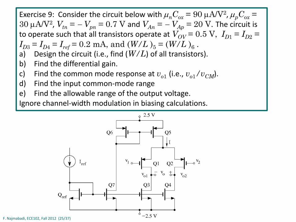
Exercise 9: Consider the circuit below with µnCox = 90 µA/V2, µpCox = 30 µA/V2, Vtn = − Vpn = 0.7 V and VAn = − VAp = 20 V. The circuit is to operate such that all transistors operate at VOV = 0.5 V, ID1 = ID2 = ID3 = ID4 = Iref = 0.2 mA, and (W/L )5 = (W/L )6 . a) Design the circuit (i.e., find (W/L) of all transistors). b) Find the differential gain. c) Find the common mode response at vo1 (i.e., vo1/vCM). d) Find the input common-mode range e) Find the allowable range of the output voltage. Ignore channel-width modulation in biasing calculations.
F. Najmabadi, ECE102, Fall 2012 (26/37)
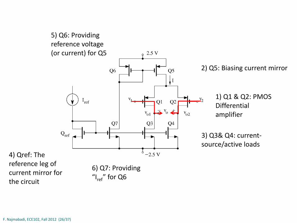
1) Q1 & Q2: PMOS Differential amplifier
2) Q5: Biasing current mirror
5) Q6: Providing reference voltage (or current) for Q5
3) Q3& Q4: current-source/active loads
6) Q7: Providing “Iref” for Q6
4) Qref: The reference leg of current mirror for the circuit
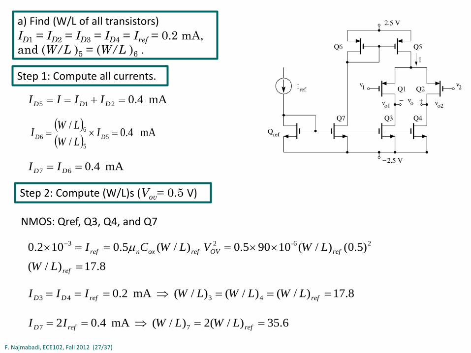
F. Najmabadi, ECE102, Fall 2012 (27/37)
8.17)/(
)5.0()/(10900.5 )/(5.0102.0 2-623
=
××===× −
ref
refOVrefoxnref
LWLWVLWCI µ
mA 4.0 215 =+== DDD IIII
a) Find (W/L of all transistors) ID1 = ID2 = ID3 = ID4 = Iref = 0.2 mA, and (W/L )5 = (W/L )6 .
Step 1: Compute all currents.
NMOS: Qref, Q3, Q4, and Q7
( )( ) mA 4.0
// 5
5
66 =×= DD I
LWLWI
mA 4.067 == DD II
Step 2: Compute (W/L)s (Vov= 0.5 V)
6.35)/(2)/( mA 4.02 77 ==⇒== refrefD LWLWII
8.17)/()/()/( mA 2.0 4343 ===⇒=== refrefDD LWLWLWIII
F. Najmabadi, ECE102, Fall 2012 (28/37)
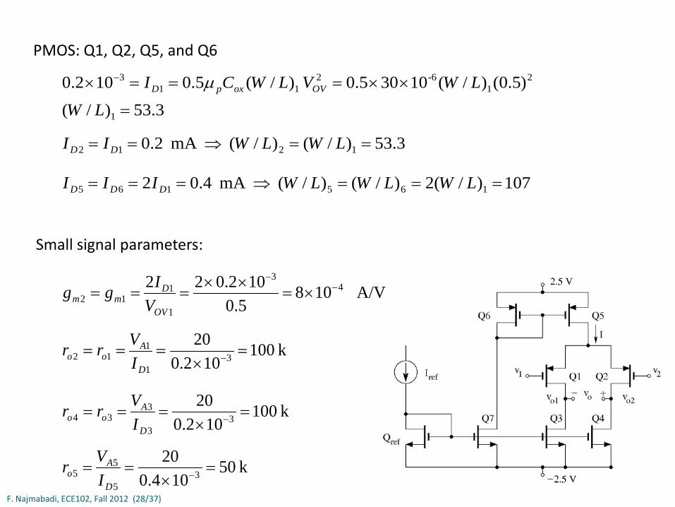
3.53)/(
)5.0()/(10300.5 )/(5.0102.0
1
21
-6211
3
=
××===× −
LWLWVLWCI OVoxpD µ
PMOS: Q1, Q2, Q5, and Q6
107)/(2)/()/( mA 4.02 165165 ===⇒=== LWLWLWIII DDD
3.53)/()/( mA 2.0 1212 ==⇒== LWLWII DD
A/V 1085.0
102.022 43
1
112
−−
×=××
===OV
Dmm V
Igg
k 001102.0
203
1
112 =
×=== −
D
Aoo I
Vrr
Small signal parameters:
k 001102.0
203
3
334 =
×=== −
D
Aoo I
Vrr
k 50104.0
203
5
55 =
×== −
D
Ao I
Vr

F. Najmabadi, ECE102, Fall 2012 (29/37)
40k)100||k100(108
)||(5.0
4
3111,
−=×−=
−=−
=
−d
oomd
dod
A
rrgv
vA
98.01801
801105010821
10100108
/21
,1,2
34
34,1
1351
31,1
−=++
−==
+××××+×××
−=
++−=
−
−
c
co
c
co
c
co
ooom
om
c
co
vv
vvv
vrrrg
rgv
v
b) Find the differential gain: c) Find common mode response, vo1:

F. Najmabadi, ECE102, Fall 2012 (30/37)
d) Find input common mode range:
1) Q5 in saturation:
2.1 V 1.2 || 11 +=⇒=+=− CMStpOVCMS VVVVVV
V 25.05.2 5.2 5155 =−≤=⇒≥−= DSOVDSD VVVVV
2) Q1/Q3 in saturation:
33
11
OVDS
OVSD
VVVV≥≥
5.1 1)5.2(V 1
11
31
−≥⇒≥−−=+≥+
SS
OVOVDSSD
VVVVVV
V 2.0 .51 1 ≤≤− SV
The above equation indicates VS1 changes and tracks VCM as VCM changes. VS1 is limited by two criteria below:
V 2.0 1.2 .51 ≤+≤− CMV
V 0.8 .72 ≤≤− CMV
Note that the requirement on Q1/Q3 in saturation is usually more restrictive than above as Q1/Q3 do not usually reach saturation together (calculation above represents “the best case”). However, correct solution requires that we include channel-width modulation and calculate the relationship between VSD1 & VDS3 (same arguments apply to part e).
F. Najmabadi, ECE102, Fall 2012 (31/37)
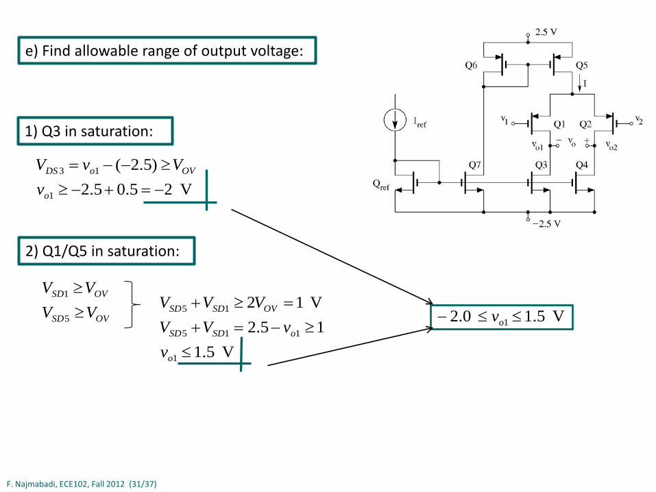
e) Find allowable range of output voltage:
1) Q3 in saturation:
V 25.05.2 )5.2(
1
13
−=+−≥≥−−=
o
OVoDS
vVvV
2) Q1/Q5 in saturation:
OVSD
OVSD
VVVV
5
1
≥≥
V 5.1 15.2
V 12
1
115
15
≤≥−=+
=≥+
o
oSDSD
OVSDSD
vvVV
VVV V 1.5 .02 1 ≤≤− ov

F. Najmabadi, ECE102, Fall 2012 (32/37)
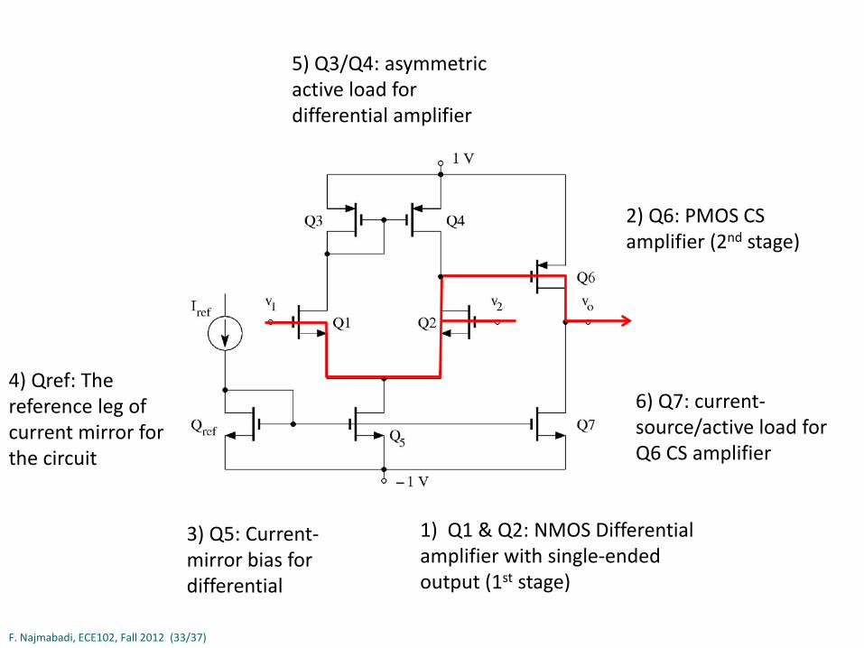
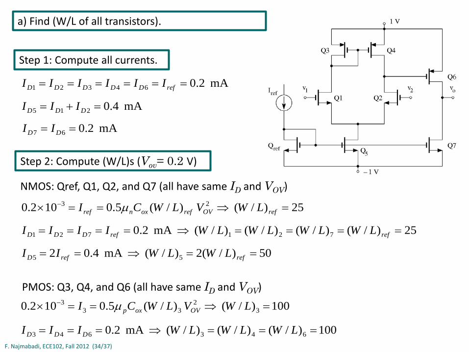
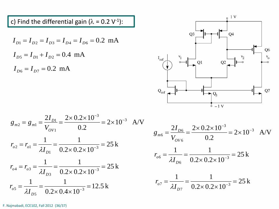
Exercise 10: Consider the circuit below with µnCox = 400 µA/V2, µpCox = 100 µA/V2, and Vtn = − Vpn = 0.4 V. All transistors operate at VOV = 0.2 V and ID1 = ID2 = ID3 = ID4 = ID6 = Iref = 0.2 mA a) Design the circuit (i.e., find (W/L) of all transistors) b) Find the input common-mode range c) Find the differential gain (λ = 0.2 V-1)
F. Najmabadi, ECE102, Fall 2012 (33/37)
1) Q1 & Q2: NMOS Differential amplifier with single-ended output (1st stage)
3) Q5: Current- mirror bias for differential
2) Q6: PMOS CS amplifier (2nd stage)
5) Q3/Q4: asymmetric active load for differential amplifier
6) Q7: current-source/active load for Q6 CS amplifier
4) Qref: The reference leg of current mirror for the circuit
F. Najmabadi, ECE102, Fall 2012 (34/37)
25)/( )/(5.0102.0 23 =⇒==× −refOVrefoxnref LWVLWCI µ
mA 4.0215 =+= DDD III
a) Find (W/L of all transistors).
Step 1: Compute all currents.
NMOS: Qref, Q1, Q2, and Q7 (all have same ID and VOV)
mA 2.067 == DD II
Step 2: Compute (W/L)s (Vov= 0.2 V)
50)/(2)/( mA 4.02 55 ==⇒== refrefD LWLWII
25)/()/()/()/( mA 2.0 721721 ====⇒==== refrefDDD LWLWLWLWIIII
mA 2.064321 ====== refDDDDD IIIIII
100)/( )/(5.0102.0 32
333 =⇒==× − LWVLWCI OVoxpµ
PMOS: Q3, Q4, and Q6 (all have same ID and VOV)
100)/()/()/( mA 2.0 643643 ===⇒=== LWLWLWIII DDD
F. Najmabadi, ECE102, Fall 2012 (35/37)
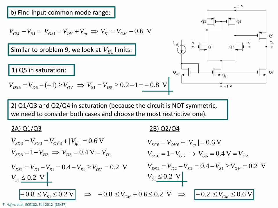
b) Find input common mode range:
1) Q5 in saturation:
V 6.0 111 −=⇒+==− CMStnOVGSSCM VVVVVVV
V 8.0 12.0 )1( 5155 −=−≥=⇒≥−−= DSOVDDS VVVVV
2) Q1/Q3 and Q2/Q4 in saturation (because the circuit is NOT symmetric, we need to consider both cases and choose the most restrictive one).
1333
333
V 0.4 1
V 0.6 ||
DDDSD
tpOVSGSD
VVVVVVVV
==⇒−=
=+==
V 0.2V 2.0 4.0
1
1111
≤=≥−=−=
S
OVSSDDS
VVVVVV
V 2.0 8.0 1 ≤≤− SV
Similar to problem 9, we look at VS1 limits:
2A) Q1/Q3
2666
66
V 0.4 1
V 0.6 ||
DGGSG
tpOVSG
VVVVVVV
==⇒−=
=+=
V 0.2V 2.0 4.0
1
1222
≤=≥−=−=
S
OVSSDDS
VVVVVV
2B) Q2/Q4
V 6.0 2.0 ≤≤− CMV⇒≤−≤−⇒ V 0.2 0.6 .80 CMV
F. Najmabadi, ECE102, Fall 2012 (36/37)
c) Find the differential gain (λ = 0.2 V-1):
A/V 1022.0
102.022 33
1
112
−−
×=××
===OV
Dmm V
Igg
k 25102.02.0
113
112 =
××=== −
Doo I
rrλ
A/V 1022.0
102.022 33
6
66
−−
×=××
==OV
Dm V
Ig
k 25102.02.0
113
66 =
××== −
Do I
rλ
k 25102.02.0
113
334 =
××=== −
Doo I
rrλ
k 5.12104.02.0
113
55 =
××== −
Do I
rλ
mA 2.064321 ===== DDDDD IIIII
mA 4.0215 =+= DDD III
mA 2.076 == DD II
k 25102.02.0
113
77 =
××== −
Do I
rλ
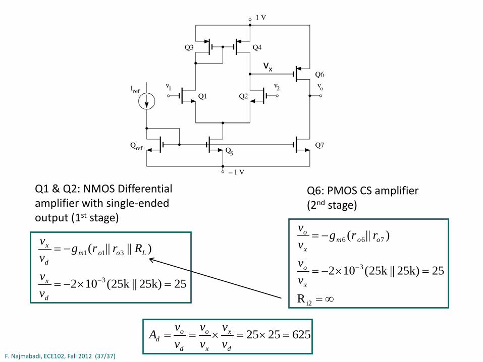
F. Najmabadi, ECE102, Fall 2012 (37/37)
Q6: PMOS CS amplifier (2nd stage)
∞=
=×−=
−=
−
i2
3
766
R
255k)2||k25(102
)||(
x
o
oomx
o
vv
rrgvv
Q1 & Q2: NMOS Differential amplifier with single-ended output (1st stage)
255k)2||k25(102
)||||(
3
311
=×−=
−=
−
d
x
Loomd
x
vv
Rrrgvv
6252525 =×=×==d
x
x
o
d
od v
vvv
vvA
vx
Top Related