


γλώσσες
Σελίδες
Νομικός


EVAL-ADAQ7980SDZ User Guide UG-1060
One Technology Way • P.O. Box 9106 • Norwood, MA 02062-9106, U.S.A. • Tel: 781.329.4700 • Fax: 781.461.3113 • www.analog.com
Evaluating the ADAQ7980 16-Bit, 1 MSPS, μModule® Data Acquisition System in LGA
PLEASE SEE THE LAST PAGE FOR AN IMPORTANT WARNING AND LEGAL TERMS AND CONDITIONS. Rev. A | Page 1 of 30
FEATURES Full featured evaluation board for the ADAQ7980 Versatile analog signal conditioning circuitry On-board reference, reference buffers, and ADC drivers SDP board-compatible (EVAL-SDP-CB1Z) PC software for control and data analysis of time and
frequency domain
EVALUATION KIT CONTENTS EVAL-ADAQ7980SDZ evaluation board Wall power supply 9 V dc adapter Daughter card power connector Nylon screws
EQUIPMENT NEEDED System demonstration platform (EVAL-SDP-CB1Z) Precision analog signal source Power supply, +7.5 V/−2.5 V (optional) USB cable SMA cable PC running Windows® XP SP2, Windows Vista, Windows 7, or
higher with USB 2.0 port
ONLINE RESOURCES ADAQ7980/ADAQ7988 data sheet EVAL-ADAQ7980SDZ user guide ADAQ798x Evaluation Software FAQs and Troubleshooting
GENERAL DESCRIPTION The EVAL-ADAQ7980SDZ is an evaluation board designed to demonstrate the low power ADAQ7980 performance and provide an easy to understand interface for a variety of system applications. The ADAQ7980 is a 16-bit, 1 MSPS, μModule data acquisition system that integrates four common signal processing and conditioning blocks into a system in package (SiP) design that supports a variety of applications.
The EVAL-ADAQ7980SDZ can also evaluate the ADAQ7988, despite being populated with the ADAQ7980. To mimic the evaluation of the ADAQ7988 performance, limit the maximum sample rate of the ADAQ7980 to 500 kSPS in the ADAQ798x Evaluation Software.
The evaluation board is ideal for use with the Analog Devices, Inc., system demonstration platform (SDP) board, EVAL-SDP-CB1Z. The EVAL-ADAQ7980SDZ interfaces to the SDP board via a 120-pin connector. P1, P2, P3, and P4 SMA connectors are provided to connect a low noise analog signal source.
The ADAQ798x Evaluation Software executable controls the evaluation board over the USB through the EVAL-SDP-CB1Z. See the Related Links section for a list of on-board components.
A full description and complete specifications for the ADAQ7980 are provided in the ADAQ7980/ADAQ7988 data sheet and must be consulted in conjunction with this user guide when using the evaluation board. Full details on the EVAL-SDP-CB1Z are available on the SDP-B product page.
UG-1060 EVAL-ADAQ7980SDZ User Guide
Rev. A | Page 2 of 30
TABLE OF CONTENTS Features .............................................................................................. 1 Evaluation Kit Contents ................................................................... 1 Equipment Needed ........................................................................... 1 Online Resources .............................................................................. 1 General Description ......................................................................... 1 Revision History ............................................................................... 2 EVAL-ADAQ7980SDZ Evaluation Board ..................................... 3 Getting Started .................................................................................. 4
Software Installation Procedures ................................................ 4 Evaluation Board Setup Procedures ........................................... 6
Evaluation Board Hardware ............................................................ 8 Hardware Overview ..................................................................... 8 Reference ....................................................................................... 8 Analog Inputs ................................................................................ 9 Power Supplies ............................................................................ 10 Digital Interface .......................................................................... 10
Link Configuration Options ......................................................... 11 Modes of Operation ....................................................................... 12
SDP Controlled Mode ................................................................ 12
User Defined Control Mode ..................................................... 12
Evaluation Board Software Setup Procedures ............................ 13 Evaluation Board Connection Sequence ................................. 13
Evaluation Board Software ............................................................ 15 Overview of the Main Window ................................................ 15 Configure Tab ............................................................................. 16 Waveform Tab ............................................................................. 17 Histogram Tab ............................................................................ 18 FFT Tab ........................................................................................ 19 Summary Tab .............................................................................. 20
Evaluation Hardware and Software Operation .......................... 21 Capturing Conversion Results .................................................. 21 Generating a Waveform Analysis Report ................................ 21 Generating a Histogram of the ADC Code Distribution ..... 21 Generating an FFT of AC Characteristics ............................... 21 Generating a Summary of the Waveform, Histogram, and Fast Fourier Transform .............................................................. 22 Operating the Evaluation Software in Standalone Mode ..... 22
Evaluation Board Schematics and Artwork ................................ 23 Related Links ................................................................................... 30
REVISION HISTORY 9/2017—Rev. 0 to Rev. A Changed Title to Evaluating the ADAQ7980 16-Bit, 1 MSPS, μModule Data Acquisition System in LGA ................................... 1 Change to General Description ...................................................... 1 Changes to Table 5 .......................................................................... 10 Change to Related Links Section .................................................. 30 3/2017—Revision 0: Initial Version
EVAL-ADAQ7980SDZ User Guide UG-1060
Rev. A | Page 3 of 30
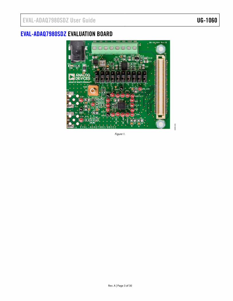
EVAL-ADAQ7980SDZ EVALUATION BOARD
Figure 1.
1506
5-00
1
UG-1060 EVAL-ADAQ7980SDZ User Guide
Rev. A | Page 4 of 30
GETTING STARTED The following section contains the installation instructions for the ADAQ798x Evaluation Software and the drivers for the SDP hardware required for operation of the software. The evaluation software provides a graphical user interface (GUI) for quick evaluation of the ADAQ7980.
SOFTWARE INSTALLATION PROCEDURES Download the evaluation board software from the ADAQ7980 product page on the Analog Devices website.
To install the software, take the following steps:
• Run the ADAQ798x Evaluation Software installation • Run the EVAL-SDP-CB1Z SDP board drivers installation
Warning
Install the evaluation board software and drivers before connecting the EVAL-ADAQ7980SDZ evaluation board and EVAL-SDP-CB1Z board to the USB port of the PC to ensure the evaluation system is correctly recognized when it connects to the PC.
Installing the ADAQ7980 Evaluation Board Software
To install the ADAQ798x Evaluation Software,
1. Start the Windows operating system and download the software from the EVAL-ADAQ7980SDZ product page on the Analog Devices website.
2. Unzip the downloaded file. 3. Double-click the setup.exe file to begin the evaluation
board software installation (see Figure 2).
Figure 2. ADAQ7980 Evaluation Board Software Installation—Installation
Begins
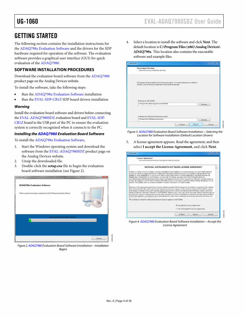
4. Select a location to install the software and click Next. The default location is C:\Program Files (x86)\Analog Devices\ ADAQ798x. This location also contains the executable software and example files.
Figure 3. ADAQ7980 Evaluation Board Software Installation—Selecting the
Location for Software Installation (Default Location Shown)
5. A license agreement appears. Read the agreement, and then select I accept the License Agreement, and click Next.
Figure 4. ADAQ7980 Evaluation Board Software Installation—Accept the
License Agreement
1506
5-00
2
1506
5-00
315
065-
004
EVAL-ADAQ7980SDZ User Guide UG-1060
Rev. A | Page 5 of 30
6. An installation summary displays. Click Next to continue.
Figure 5. ADAQ7980 Evaluation Board Software Installation—
Installation Summary
7. A dialog box shows the installation progress.
Figure 6. ADAQ7980 Evaluation Board Software Installation—
Installation Progress
8. The dialog box informs the user when the installation is complete. Click Finish.
Figure 7. ADAQ7980 Evaluation Board Software Installation—
Installation Complete
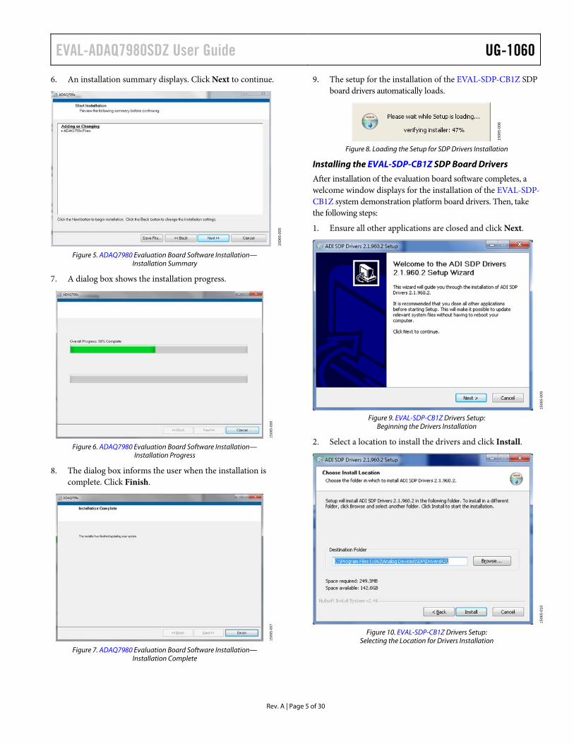
9. The setup for the installation of the EVAL-SDP-CB1Z SDP board drivers automatically loads.
Figure 8. Loading the Setup for SDP Drivers Installation
Installing the EVAL-SDP-CB1Z SDP Board Drivers
After installation of the evaluation board software completes, a welcome window displays for the installation of the EVAL-SDP-CB1Z system demonstration platform board drivers. Then, take the following steps:
1. Ensure all other applications are closed and click Next.
Figure 9. EVAL-SDP-CB1Z Drivers Setup:
Beginning the Drivers Installation
2. Select a location to install the drivers and click Install.
Figure 10. EVAL-SDP-CB1Z Drivers Setup:
Selecting the Location for Drivers Installation
1506
5-00
5
1506
5-00
615
065-
007
1506
5-00
8
1506
5-00
915
065-
010
UG-1060 EVAL-ADAQ7980SDZ User Guide
Rev. A | Page 6 of 30
3. Installation of the SDP drivers begins.
Figure 11. EVAL-SDP-CB1Z Drivers Setup—Beginning the Installation
4. A dialog box appears asking to install the SDP software available with the EVAL-SDP-CB1Z. Click Install.
Figure 12. EVAL-SDP-CB1Z Drivers Setup—Granting Permission
to Install Drivers
5. To complete the drivers installation, click Finish, which closes the installation wizard.
Figure 13. EVAL-SDP-CB1Z Drivers Setup:
Completing the Drivers Setup Wizard
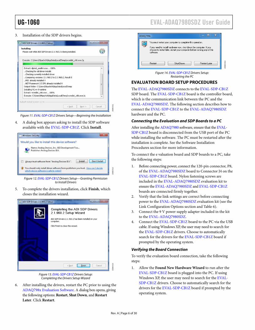
6. After installing the drivers, restart the PC prior to using the ADAQ798x Evaluation Software. A dialog box opens, giving the following options: Restart, Shut Down, and Restart Later. Click Restart.
Figure 14. EVAL-SDP-CB1Z Drivers Setup:
Restarting the PC
EVALUATION BOARD SETUP PROCEDURES The EVAL-ADAQ7980SDZ connects to the EVAL-SDP-CB1Z SDP board. The EVAL-SDP-CB1Z board is the controller board, which is the communication link between the PC and the EVAL-ADAQ7980SDZ. The following section describes how to connect the EVAL-SDP-CB1Z to the EVAL-ADAQ7980SDZ hardware and the PC.
Connecting the Evaluation and SDP Boards to a PC
After installing the ADAQ7980 software, ensure that the EVAL-SDP-CB1Z board is disconnected from the USB port of the PC while installing the software. The PC must be restarted after the installation is complete. See the Software Installation Procedures section for more information.
To connect the e valuation board and SDP boards to a PC, take the following steps:
1. Before connecting power, connect the 120-pin connector, P8, of the EVAL-ADAQ7980SDZ board to Connector J4 on the EVAL-SDP-CB1Z board. Nylon fastening screws are included in the EVAL-ADAQ7980SDZ evaluation kit to ensure the EVAL-ADAQ7980SDZ and EVAL-SDP-CB1Z boards are connected firmly together.
2. Verify that the link settings are correct before connecting power to the EVAL-ADAQ7980SDZ evaluation kit (see the Link Configuration Options section and Table 6).
3. Connect the 9 V power supply adapter included in the kit to the EVAL-ADAQ7980SDZ.
4. Connect the EVAL-SDP-CB1Z board to the PC via the USB cable. If using Windows XP, the user may need to search for the EVAL-SDP-CB1Z drivers. Choose to automatically search for the drivers for the EVAL-SDP-CB1Z board if prompted by the operating system.
Verifying the Board Connection
To verify the evaluation board connection, take the following steps:
1. Allow the Found New Hardware Wizard to run after the EVAL-SDP-CB1Z board is plugged into the PC. If using Windows XP, the user may need to search for the EVAL-SDP-CB1Z drivers. Choose to automatically search for the drivers for the EVAL-SDP-CB1Z board if prompted by the operating system.
1506
5-01
115
065-
012
1506
5-01
3
1506
5-01
4
EVAL-ADAQ7980SDZ User Guide UG-1060
Rev. A | Page 7 of 30
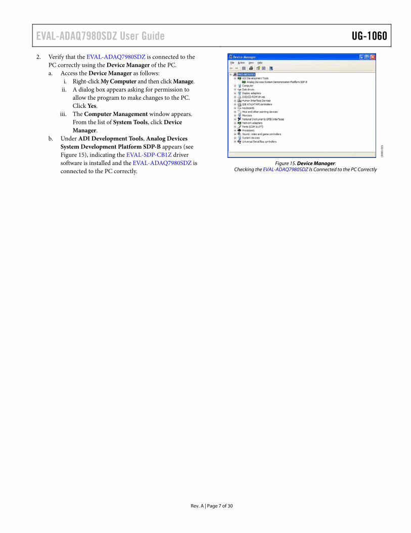
2. Verify that the EVAL-ADAQ7980SDZ is connected to the PC correctly using the Device Manager of the PC. a. Access the Device Manager as follows:
i. Right-click My Computer and then click Manage. ii. A dialog box appears asking for permission to
allow the program to make changes to the PC. Click Yes.
iii. The Computer Management window appears. From the list of System Tools, click Device Manager.
b. Under ADI Development Tools, Analog Devices System Development Platform SDP-B appears (see Figure 15), indicating the EVAL-SDP-CB1Z driver software is installed and the EVAL-ADAQ7980SDZ is connected to the PC correctly.
1506
5-01
5
Figure 15. Device Manager:
Checking the EVAL-ADAQ7980SDZ Is Connected to the PC Correctly
UG-1060 EVAL-ADAQ7980SDZ User Guide
Rev. A | Page 8 of 30
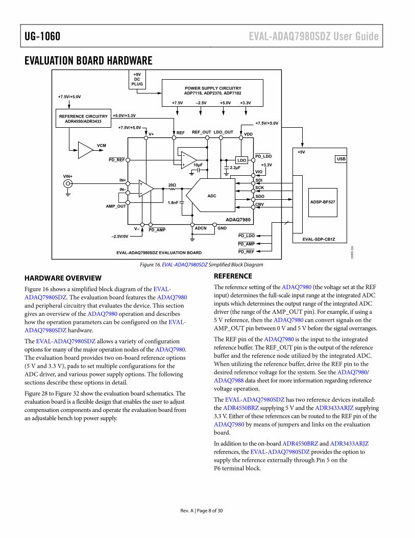
EVALUATION BOARD HARDWARE
VIN+
EVAL-ADAQ7980SDZ EVALUATION BOARD
ADC
REF
GND
VDD
IN+
IN–
VIO
SDI
SCK
SDO
CNV
20Ω
V+
V–
1.8nF
10µFLDO
2.2µF
REF_OUT LDO_OUT
PD_REF
AMP_OUT
PD_AMP
PD_LDO
+7.5V/+5.0V+7.5V/+5.0V
+3.3V
–2.5V/0V
ADCN
ADAQ7980
PD_LDO
PD_AMP
PD_REF
POWER SUPPLY CIRCUITRYADP7118, ADP2370, ADP7182
+7.5V +5.0V–2.5V +3.3V
+9VDC
PLUG
REFERENCE CIRCUITRYADR4550/ADR3433
+5.0V/+3.3V
+7.5V/+5.0V
VCM
ADSP-BF527
EVAL-SDP-CB1Z
+5V
USB
1506
5-11
6
Figure 16. EVAL-ADAQ7980SDZ Simplified Block Diagram
HARDWARE OVERVIEW Figure 16 shows a simplified block diagram of the EVAL-ADAQ7980SDZ. The evaluation board features the ADAQ7980 and peripheral circuitry that evaluates the device. This section gives an overview of the ADAQ7980 operation and describes how the operation parameters can be configured on the EVAL-ADAQ7980SDZ hardware.
The EVAL-ADAQ7980SDZ allows a variety of configuration options for many of the major operation nodes of the ADAQ7980. The evaluation board provides two on-board reference options (5 V and 3.3 V), pads to set multiple configurations for the ADC driver, and various power supply options. The following sections describe these options in detail.
Figure 28 to Figure 32 show the evaluation board schematics. The evaluation board is a flexible design that enables the user to adjust compensation components and operate the evaluation board from an adjustable bench top power supply.
REFERENCE The reference setting of the ADAQ7980 (the voltage set at the REF input) determines the full-scale input range at the integrated ADC inputs which determines the output range of the integrated ADC driver (the range of the AMP_OUT pin). For example, if using a 5 V reference, then the ADAQ7980 can convert signals on the AMP_OUT pin between 0 V and 5 V before the signal overranges.
The REF pin of the ADAQ7980 is the input to the integrated reference buffer. The REF_OUT pin is the output of the reference buffer and the reference node utilized by the integrated ADC. When utilizing the reference buffer, drive the REF pin to the desired reference voltage for the system. See the ADAQ7980/ ADAQ7988 data sheet for more information regarding reference voltage operation.
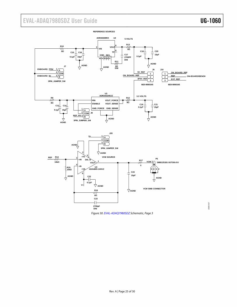
The EVAL-ADAQ7980SDZ has two reference devices installed: the ADR4550BRZ supplying 5 V and the ADR3433ARJZ supplying 3.3 V. Either of these references can be routed to the REF pin of the ADAQ7980 by means of jumpers and links on the evaluation board.
In addition to the on-board ADR4550BRZ and ADR3433ARJZ references, the EVAL-ADAQ7980SDZ provides the option to supply the reference externally through Pin 5 on the P6 terminal block.
EVAL-ADAQ7980SDZ User Guide UG-1060
Rev. A | Page 9 of 30
Table 1 shows the configurations required for using the two on-board references and an external reference.
Table 1. On-Board Reference Options Provided on the EVAL-ADAQ7980SDZ
On-Board Reference Voltage (V)
On-Board Reference Devices Link Settings
5 ADR4550BRZ J7 at A
J9 at 1
J10 at 1
3.3 ADR3433ARJZ J7 at B1
J9 at 3
J10 at 1
External Reference Voltage
External device J10 at 3
1 The J7 configuration is set to ensure the voltage input of the ADR3433ARJZ is
within its specified range (<5.5 V).
The ADR4550BRZ and ADR3433ARJZ also supply the VCM node, which can be used as a dc bias or common-mode voltage for the analog-to-digital converter (ADC) driver. Figure 30 shows the circuitry generating VCM. See the Analog Inputs section for more information on VCM operation.
ANALOG INPUTS This section describes how to apply analog inputs to the EVAL-ADAQ7980SDZ.
The ADAQ7980 contains an ADC driver. The user has access to the noninverting and inverting inputs and output of the ADC driver (IN+, IN−, and AMP_OUT, respectively), which allows configurability of the driver by means of jumper settings and passive components. Figure 17 shows the ADC driver connection diagram, including all relevant jumpers and passive components for configuration.
Figure 17. Relevant Links and Components for Configuring the ADC Driver
The ADC input accepts unipolar signals between ground and the voltage set by the integrated reference buffer (voltage on the REF and REF_OUT pins). Therefore, the ADC driver outputs must be limited to ground and the voltage on REF_OUT as well. Because the signal is unipolar, the input signal must include a dc offset component, typically to REF/2.
If the input source cannot supply the dc bias, a common-mode voltage generated on board (labeled VCM in Figure 17) can connect to the noninverting input of the ADC driver through the R22 resistor. VCM is set to REF/2 by default. Use the R22 and R24 resistors to set VCM to another desired dc voltage. See the Reference section for more information on VCM.
Table 2 outlines the link settings and passive components that implement common ADC driver configurations.
Table 2. ADC Driver Configuration Settings
Configuration Link Settings Component
Noninverting Unity-Gain Buffer
J1 at A Do not populate R20
R21 at 0 Ω
Do not populate R22
R23 at 0 Ω
Do not populate R24
Inverting with Level Shift
J1 at B, J2 at A, and J3 at A
Select R20 and R23 for desired gain
Do not populate R21
R22 and R24 selected for desired dc setting
Noninverting with Nonunity Gain
J1 at A and J3 at B
Select R20 and R23 for desired gain
R21 at 0 Ω
Do not populate R22 and R24
Noninverting Unity-Gain Buffer with Level Shift
J1 at A Do not populate R20
R21 = R22 ≠ 0 Ω
R23 at 0 Ω
Select R24 for desired dc setting
The EVAL-ADAQ7980SDZ is configured by factory default with the ADC driver in a unity-gain configuration. The dc offset needed for unipolar signals can be provided either by the signal source or by using the on-board dc offset VCM.
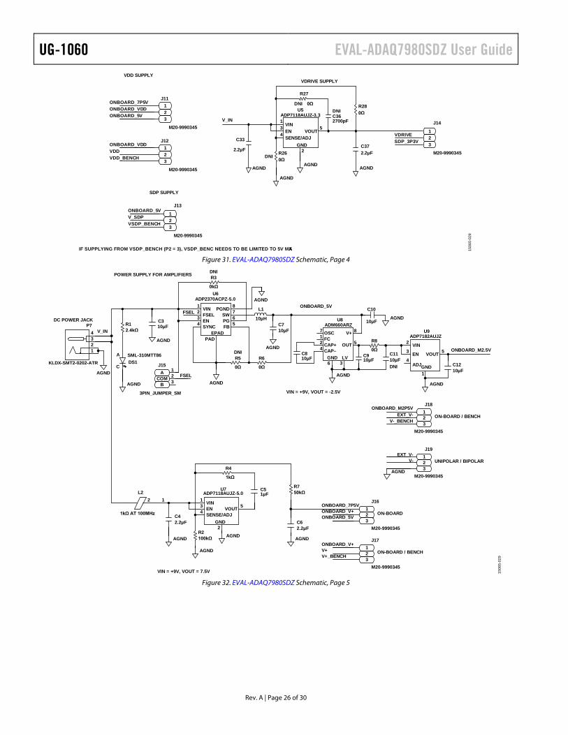
The analog inputs to the EVAL-ADAQ7980SDZ are the P1 to P4 SMA connectors. The input circuit arrangement is controlled by the settings of J1 to J3. The circuit not only allows different configurations, input range scaling, and filtering, but it also allows adding a dc component. The analog input amplifiers are set as unity-gain buffers by factory default. The amplifier positive rail is driven from 7.5 V from U7 (ADP7118). The amplifier negative rail is driven from −2.5 V, generated by U9 (ADP7182).
A differential output source can also drive the EVAL-ADAQ7980SDZ inputs as long as the output of the source can be biased to the midscale (either internally or externally). The P3 and P4 connectors and the R18/R19 voltage divider balance termination of the signal source.
VCM
VCM
C25 C27R24
R21IN–
IN+
R20 R23
C26
R22
J1VIN+
AMP_OUT
J2
A
AA
BB
B
J3
1506
5-11
7
UG-1060 EVAL-ADAQ7980SDZ User Guide
Rev. A | Page 10 of 30
For dynamic performance, conduct a fast Fourier transform (FFT) test by applying a very low distortion ac source.
For low frequency testing, an instrument like an audio precision source (such as the SYS-2700 series) can be used directly because its outputs are isolated. Set the outputs as balanced with a floating ground. The P3 and P4 connectors balance termination of a signal source. Different sources can be used; however, most are single-ended sources that use a fixed output resistance.
POWER SUPPLIES The evaluation board can be powered from a wall adapter or from a bench top power supply. By default, the EVAL-ADAQ7980SDZ is set up to operate from a 9 V wall adapter using the on-board power supplies described in Table 3.
Table 3. Power Supplies Provided on the EVAL-ADAQ7980SDZ
Power Supply (V) Default Function On-Board Components
+5 SDP power ADP2370-5.0
+7.5 V+ and VDD supply ADP7118
−2.5 V− supply ADP7182
+3.3 VDRIVE (VIO supply) ADP7118-3.3
Each on-board power supply is decoupled where it enters the EVAL-ADAQ7980SDZ as well as at the power pins of each of the on-board components. A single ground plane on the evaluation board minimizes the effect of high frequency noise interference.
The EVAL-ADAQ7980SDZ provides multiple power scheme options by means of various link settings on the evaluation board. These options allow evaluation of the ADAQ7980 with various power configurations. By default, the EVAL-ADAQ7980SDZ is configured as shown in Table 1. Table 4 lists the different supply settings available.
Table 4. Alternate Power Supply Options ADAQ7980 Power Pin Pin Function
On-Board Power Options (V)
VDD Input to LDO powering the ADC
+7.5 and +5
V+ ADC driver and reference buffer positive supply
+7.5 and +5
V− ADC driver and reference buffer negative supply
−2.5 and 0
To evaluate the ADAQ7980 in a single-supply configuration, connect the V− pin to ground and connect the V+ and VDD pins to either 7.5 V or 5 V. If V+ is set to 5 V, the device is not able to use a 5 V reference voltage.
Alternatively, power the EVAL-ADAQ7980SDZ from a bench top power supply by using the P6 terminal block. Individual supplies can also be supplied externally through P6, but also require changing the position of the relevant solder link (see Table 5). When using bench top power, use of the wall adapter and the on-board power supplies are no longer required.
Table 5. Solder Links—Settings for Bench Top Power Supply1 Link Setting Function J17 3 V+_BENCH J18 3 V−_BENCH J13 3 VSDP_BENCH J12 3 VDD_BENCH
1 See Table 6 for all other link settings.
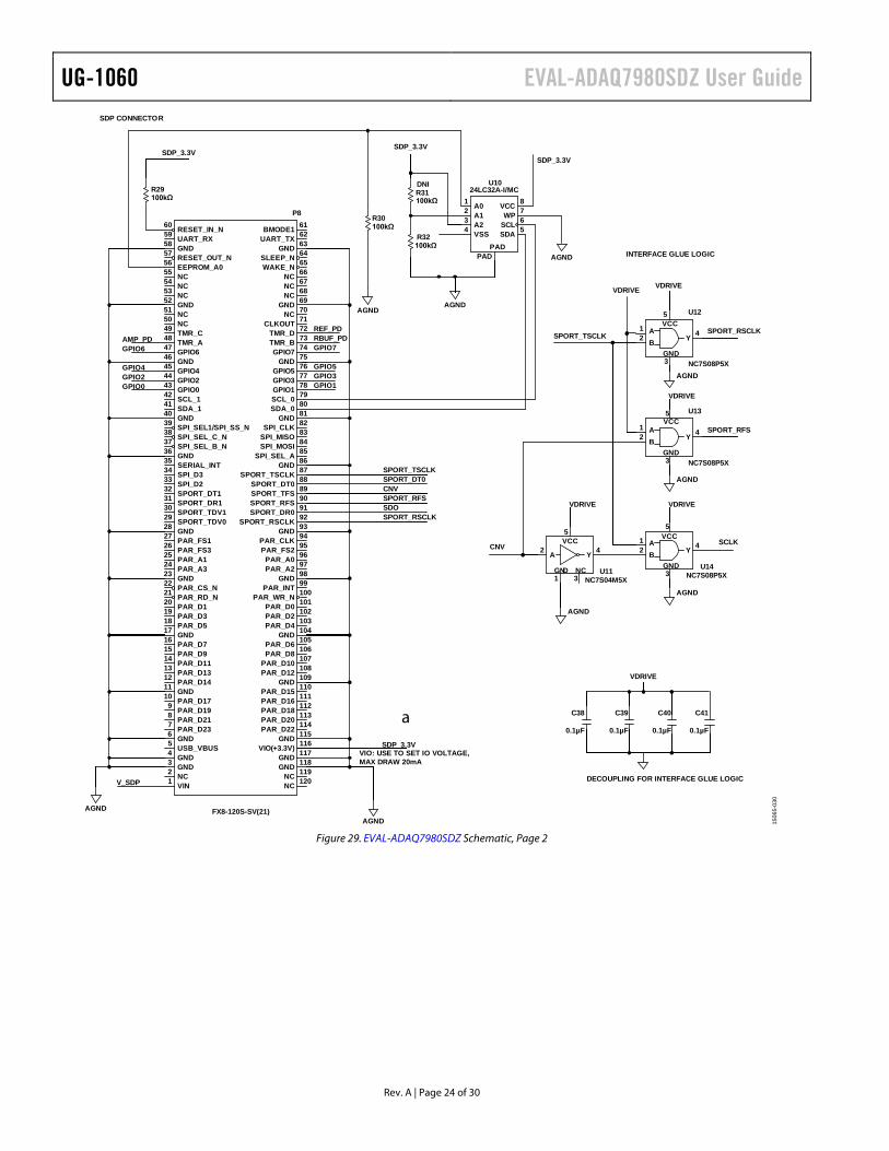
DIGITAL INTERFACE The evaluation board uses the synchronous serial peripheral port (SPORT) interface from the ADSP-BF527 digital signal processor (DSP) on the EVAL-SDP-CB1Z to control the digital interface, for example, initiating conversion and data readback, of the ADAQ7980. Multiple AND gates (U12, U13, and U14) clock and gate the SPORT transfer to the ADAQ7980.
The evaluation board also provides optional connections between the ADSP-BF527 DSP and the PD_REF and PD_AMP inputs on the EVAL-ADAQ7980SDZ through Link J4 and J5, respectively. These connections allow software controlled dynamic power scaling (DPS) of the ADC driver and reference buffer, which greatly reduces overall power consumption. For more details on implementing DPS with the ADAQ7980, consult the ADAQ7980/ADAQ7988 data sheet.
The ADAQ7980 PD_LDO input can also be connected to the ADSP-BF527 DSP by means of Link J6. This further reduces power consumption during long periods of inactivity. Power cycling the ADAQ7980 integrated low dropout regulator (LDO) requires a longer time than the ADC driver and reference buffer, however, and may not be possible for many DPS applications. See the ADAQ7980/ADAQ7988 data sheet for power-down timing specifications for each of the components.
EVAL-ADAQ7980SDZ User Guide UG-1060
Rev. A | Page 11 of 30
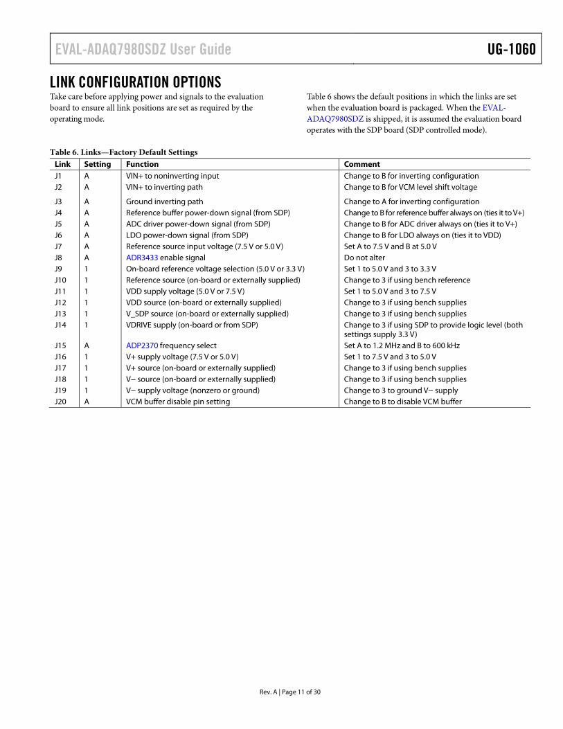
LINK CONFIGURATION OPTIONS Take care before applying power and signals to the evaluation board to ensure all link positions are set as required by the operating mode.
Table 6 shows the default positions in which the links are set when the evaluation board is packaged. When the EVAL-ADAQ7980SDZ is shipped, it is assumed the evaluation board operates with the SDP board (SDP controlled mode).
Table 6. Links—Factory Default Settings Link Setting Function Comment J1 A VIN+ to noninverting input Change to B for inverting configuration J2 A VIN+ to inverting path Change to B for VCM level shift voltage
J3 A Ground inverting path Change to A for inverting configuration J4 A Reference buffer power-down signal (from SDP) Change to B for reference buffer always on (ties it to V+) J5 A ADC driver power-down signal (from SDP) Change to B for ADC driver always on (ties it to V+) J6 A LDO power-down signal (from SDP) Change to B for LDO always on (ties it to VDD) J7 A Reference source input voltage (7.5 V or 5.0 V) Set A to 7.5 V and B at 5.0 V J8 A ADR3433 enable signal Do not alter J9 1 On-board reference voltage selection (5.0 V or 3.3 V) Set 1 to 5.0 V and 3 to 3.3 V J10 1 Reference source (on-board or externally supplied) Change to 3 if using bench reference J11 1 VDD supply voltage (5.0 V or 7.5 V) Set 1 to 5.0 V and 3 to 7.5 V J12 1 VDD source (on-board or externally supplied) Change to 3 if using bench supplies J13 1 V_SDP source (on-board or externally supplied) Change to 3 if using bench supplies J14 1 VDRIVE supply (on-board or from SDP) Change to 3 if using SDP to provide logic level (both
settings supply 3.3 V) J15 A ADP2370 frequency select Set A to 1.2 MHz and B to 600 kHz J16 1 V+ supply voltage (7.5 V or 5.0 V) Set 1 to 7.5 V and 3 to 5.0 V J17 1 V+ source (on-board or externally supplied) Change to 3 if using bench supplies J18 1 V− source (on-board or externally supplied) Change to 3 if using bench supplies J19 1 V− supply voltage (nonzero or ground) Change to 3 to ground V− supply J20 A VCM buffer disable pin setting Change to B to disable VCM buffer
UG-1060 EVAL-ADAQ7980SDZ User Guide
Rev. A | Page 12 of 30
MODES OF OPERATION SDP CONTROLLED MODE The ADAQ7980 uses a high speed serial interface that allows sampling rates of up to 1 MSPS. For more information about the operation of the serial interface, refer to the ADAQ7980/ ADAQ7988 data sheet.
The ADAQ7980 uses the serial interface to transfer data to the EVAL-SDP-CB1Z.
The EVAL-ADAQ7980SDZ communicates with the EVAL-SDP-CB1Z board using a 3.3 V logic level. Logic voltages that exceed 3.3 V can damage the SDP interface.
USER DEFINED CONTROL MODE The EVAL-ADAQ7980SDZ can also be used without the EVAL-SDP-CB1Z controller board. In this case, the EVAL-ADAQ7980SDZ connects to the serial interface using the P8 connector or the test points. For more information about the operation of the serial interface, refer to the ADAQ7980/ADAQ7988 data sheet.
EVAL-ADAQ7980SDZ User Guide UG-1060
Rev. A | Page 13 of 30
EVALUATION BOARD SOFTWARE SETUP PROCEDURES EVALUATION BOARD CONNECTION SEQUENCE With the evaluation software installed, use the following evaluation board operation/connection sequence:
1. Connect the SDP controller board to the evaluation board via the P8 connector (secure the connection using nylon screws). The software is configured to find the evaluation board on the J2 connector of the SDP board.
2. Power the EVAL-ADAQ7980SDZ with the appropriate supply, as described in the Power Supplies section.
3. Connect the EVAL-SDP-CB1Z board to a PC using the USB cable.
4. Start the evaluation software. Click Start > All Programs > Analog Devices > ADAQ798x > ADAQ798x Evaluation Software.
When the software starts running, it searches for Analog Devices hardware connected to the PC, first attempting to detect and connect to any SDP boards connected to the PC via the USB ports. If SDP boards are connected, the software attempts to detect the EVAL-ADAQ7980SDZ evaluation board connected to the SDP board. If the EVAL-ADAQ7980SDZ connects, the software runs in the standard operation mode. If it does not connect, a dialog box appears and prompts the user to either repeat the connection attempt or run the software in standalone mode.
With Hardware Connected
To run the program with hardware connected,
1. Follow Step 1 to Step 4 in the Evaluation Board Connection Sequence section.
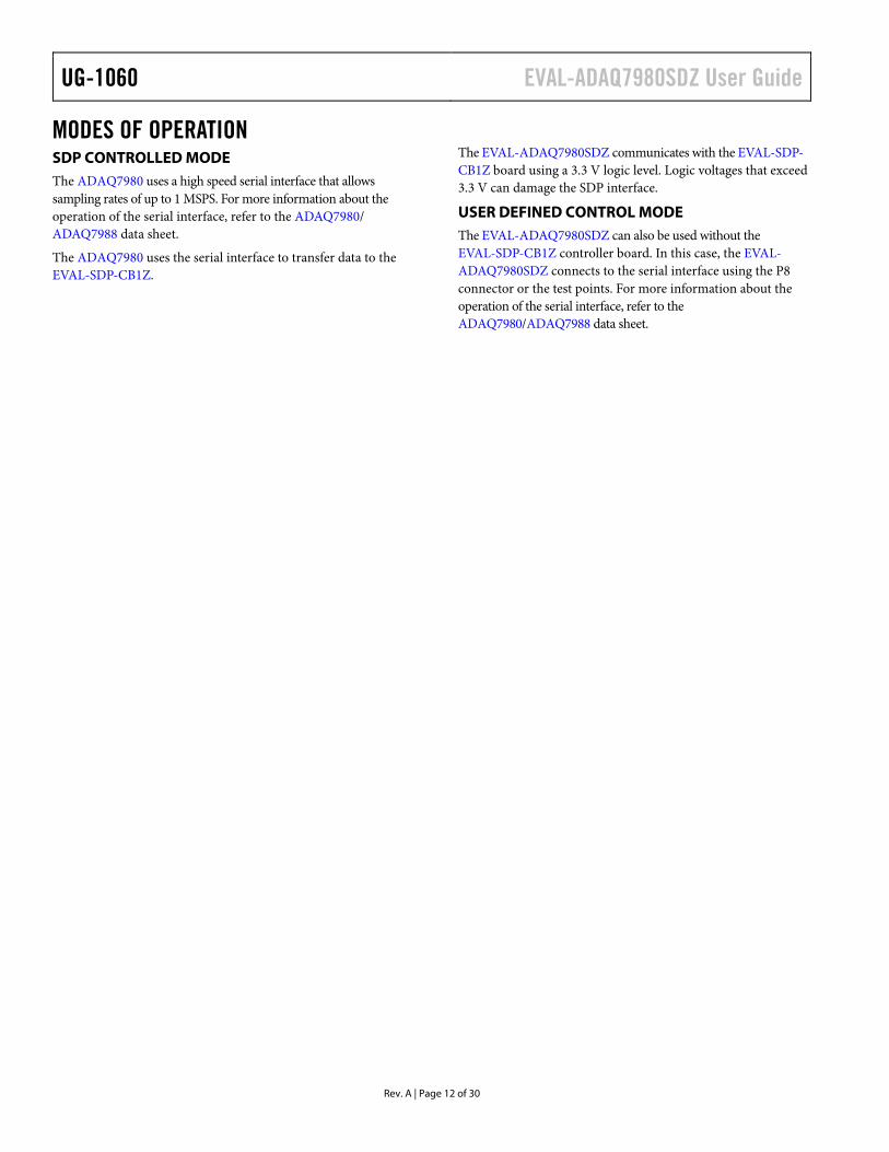
2. The software then attempts to connect to the SDP board and the EVAL-ADAQ7980SDZ. If the SDP board is not found, an error window displays (see Figure 18). If the SDP board is found but the EVAL-ADAQ7980SDZ is not detected, a different error window displays (see Figure 19). If either connectivity error displays, ensure the hardware is properly connected to the USB port of the PC, wait a few seconds, click Rescan, and follow the instructions.
Figure 18. SDP Board Not Connected to the USB Port Pop-Up Window Error
Figure 19. EVAL-ADAQ7980SDZ Not Connected to the USB Port Pop-Up
Window Error
3. After finding the evaluation board, the software connects to the EVAL-ADAQ7980SDZ and displays the pop-up window shown in Figure 20.
Figure 20. Software Connects to SDP Board
4. After the EVAL-ADAQ7980SDZ is detected, the main window of the software appears (see Figure 22), showing that the EVAL-ADAQ7980SDZ is connected.
Without Hardware Connected
The software can run in standalone mode when no evaluation board hardware is connected to the USB port. Use this mode to load previously saved states of the ADAQ798x Evaluation Software and view previously captured sets of data in the various windows of the software.
1. Click Start > All Programs > Analog Devices > ADAQ798x > ADAQ798x Evaluation Software.
2. The software attempts to connect to the evaluation hardware. If the hardware is not found, either of the error messages in Figure 18 or Figure 19 display. To continue without hardware in standalone mode, click Cancel.
1506
5-11
8
1506
5-01
6
1506
5-01
7
UG-1060 EVAL-ADAQ7980SDZ User Guide
Rev. A | Page 14 of 30
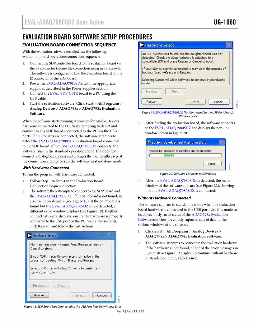
3. If operating in standalone mode, the window in Figure 21 displays.
Figure 21. Software Indicates Operating in Standalone Mode
4. Load example files or previously saved files via File > Load data. The contents of the loaded file update the various plots in the software.
5. To connect the EVAL-ADAQ7980SDZ and run the software in standard operation, close and relaunch the software to allow it to repeat the search for the SDP board and the EVAL-ADAQ7980SDZ evaluation board.
1506
5-01
8
EVAL-ADAQ7980SDZ User Guide UG-1060
Rev. A | Page 15 of 30
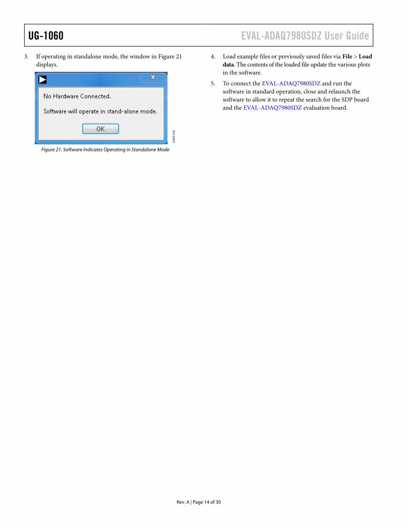
EVALUATION BOARD SOFTWARE
Figure 22. GUI Main Window
The following section gives a detailed description of the various controls and indicators in the ADAQ798x Evaluation Software. For instructions on how to capture and analyze data, see the Evaluation Hardware and Software Operation section.
OVERVIEW OF THE MAIN WINDOW The main window of the software is shown in Figure 22. The following sections describe the various controls that are accessible via this window.
File Menu
The File menu provides the following options:
• Load data—load previously captured data. • Save Data as .tsv—save captured data in .tsv format for
future analysis. • Save Picture—save the current screen capture as a JPEG file. • Print—print the current window to the default printer. • Exit—close the application.
Edit Menu
The Edit dropdown menu provides the Reinitialize Default Values option that resets controls to their default state.
Help Menu
The Help menu provides the following options:
• The Analog Devices Website option opens the Analog Devices website in the default browser.
• The User Guide option opens the EVAL-ADAQ7980SDZ user guide.
• The Context Help option opens a window containing information about the controls of the software. Help text displays in the window when the mouse hovers over a control.
• The About option opens a window displaying the software version information.
Tabs
There are five tabs available in the tabs area of the main window: Configure, Waveform, Histogram, FFT, and Summary. These tabs display the data in different formats. Navigation tools are provided within each tab to allow the user to control the cursor, zooming, and panning (see Figure 23) within the graphs displayed.
Each tab and their respective controls and functions are described in the following sections.
Single Capture Button
Click Single Capture to perform a single set of captures from the ADC. The number of captures is determined by the value in Num Samples.
Continuous Capture Button
Click Continuous Capture to perform repeated sets of captures from the ADC. The number of samples per capture set is determined by the value in Num Samples.
Num Samples Dropdown Box
The Num Samples dropdown box allows the user to select the number of samples to analyze per capture window.
Busy Indicator
The Busy indicator indicates when the software is performing operations, for example, when running conversions and analysis.
Exit Button
Click the Exit button to close the software; alternatively, users can select Exit from the File menu.
1506
5-02
0
UG-1060 EVAL-ADAQ7980SDZ User Guide
Rev. A | Page 16 of 30
CONFIGURE TAB The following contains information on the various controls accessible in the Configure tab.
Eval Board Connected Field
The Eval Board Connected field displays EVAL-ADAQ7980 when the evaluation board is connected to the USB port.
When an evaluation board is not connected to the USB port, the software can operate in standalone mode for data analysis.
ADC Settings
The ADC Settings allow changing the sampling rate and serial clock frequency via the Sampling Freq (Hz) field and SCLK Frequency (MHz) dropdown menu, respectively.
The reference voltage for the ADAQ7980 must be specified in the Reference Voltage (V) field. Use this field for data analysis only; it does not alter nor detect the reference voltage on the EVAL-ADAQ7980SDZ. For correct data interpretation, input the reference voltage being used on the evaluation board.
By default, the external reference voltage is 5 V (ADR4550 on-board reference). The minimum and maximum voltage calculations are based on this reference voltage. When changing the reference voltage, change this input accordingly.
The Sampling Freq (Hz) field sets the sample rate of the ADAQ7980, which is equivalent to the frequency of the contingent negative variation (CNV) signal of the device. The maximum sample rate of the ADAQ7980 is 1 MHz; therefore, the Sampling Freq (Hz) field does not allow values larger than 1,000,000. This control can interpret SI prefixes. Units can be entered as, for example, 10k for 10,000 Hz.
Oversampling Ratio
The Oversampling Ratio dropdown menu allows users to select the oversampling ratio to improve system dynamic range. The oversampling ratio is calculated as 22N, where N is the number of bits selected. For example, if N is selected as 2, then 16 consecutive samples are averaged together to produce one sample. This effectively reduces the ADC Nyquist rate by a factor of the over-sampling ratio, but at the benefit of increased resolution.
Dynamic Power Scaling
The Dynamic Power Scaling pane provides dynamic power scaling (DPS) configuration options for both the ADC driver and the reference buffer. DPS is a power-saving functionality of the ADAQ7980. See the ADAQ7980/ADAQ7988 data sheet for a description of DPS.
Both ADC driver DPS settings are controlled by the ADC Driver Scaling Enabled OFF/ON box, the PD_AMP On Time field, and PD Signal Phase Shift field. The reference buffer DPS settings are controlled by the Reference Buffer Scaling Enabled OFF/ON check box, the PD_REF On Time field, and the PD Signal Delta field. These controls do the following:
• ADC Driver Scaling Enabled OFF/ON activates DPS for the ADC driver when checked. When unchecked, DPS is deactivated, leaving the device on constantly.
• PD_AMP On Time sets the ADC driver on time in a sample period. If the value in PD_AMP On Time is larger than the sample period, the amplifier remain actives.
• PD Signal Phase Shift sets the offset of the ADC driver on time relative to the CNV signal.
• Reference Buffer Scaling Enabled OFF/ON activates DPS for the reference buffer when checked. When unchecked, DPS is deactivated, leaving the device on constantly.
• PD_REF On Time sets the reference buffer on time in a sample period. If the value in PD_REF On Time is larger than the sample period, the amplifier remains active.
• PD Signal Delta sets the offset of the reference buffer on time relative to the CNV signal.
Power Down LDO Button
The Power Down LDO button powers down the ADAQ7980 integrated LDO, which allows evaluation of the power consumption of the ADAQ7980 while in its power-down state.
The Power Down LDO button is not part of the evaluation software DPS functionality (see the Dynamic Power Scaling section for more information).
Flash LED Button
The Flash LED button flashes the LED on the EVAL-SDP-CB1Z board. Verify that the EVAL-ADAQ7980SDZ and the EVAL-SDP-CB1Z are connected.
EVAL-ADAQ7980SDZ User Guide UG-1060
Rev. A | Page 17 of 30
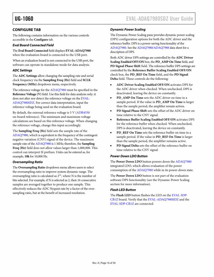
Figure 23. Waveform Tab
WAVEFORM TAB The following sections contain information on the contents of the Waveform tab (see Figure 23).
Waveform Plot
The waveform plot displays the raw ADAQ7980 results obtained during the most recent capture burst. See the Generating a Waveform Analysis Report section for more information.
Waveform Analysis
The Waveform Analysis pane displays important analysis parameters on the data in the waveform plot. The indicators (except Frequency) are displayed in both volts (V) and codes (LSB). The analysis items reference the signal at the AMP_OUT pin of the ADAQ7980.
The indicators include the following:
• Pk-pk Amplitude displays the difference between the maximum and minimum values in the data.
• Max Amplitude displays the maximum value in the data. • Min Amplitude displays the minimum value in the data. • Mean displays the average value of the data. • Standard Deviation displays the standard deviation of
the data. • Frequency displays the frequency with the largest
amplitude in the data and is only displayed in kHz (see FFT Analysis section).
1506
5-02
1
UG-1060 EVAL-ADAQ7980SDZ User Guide
Rev. A | Page 18 of 30
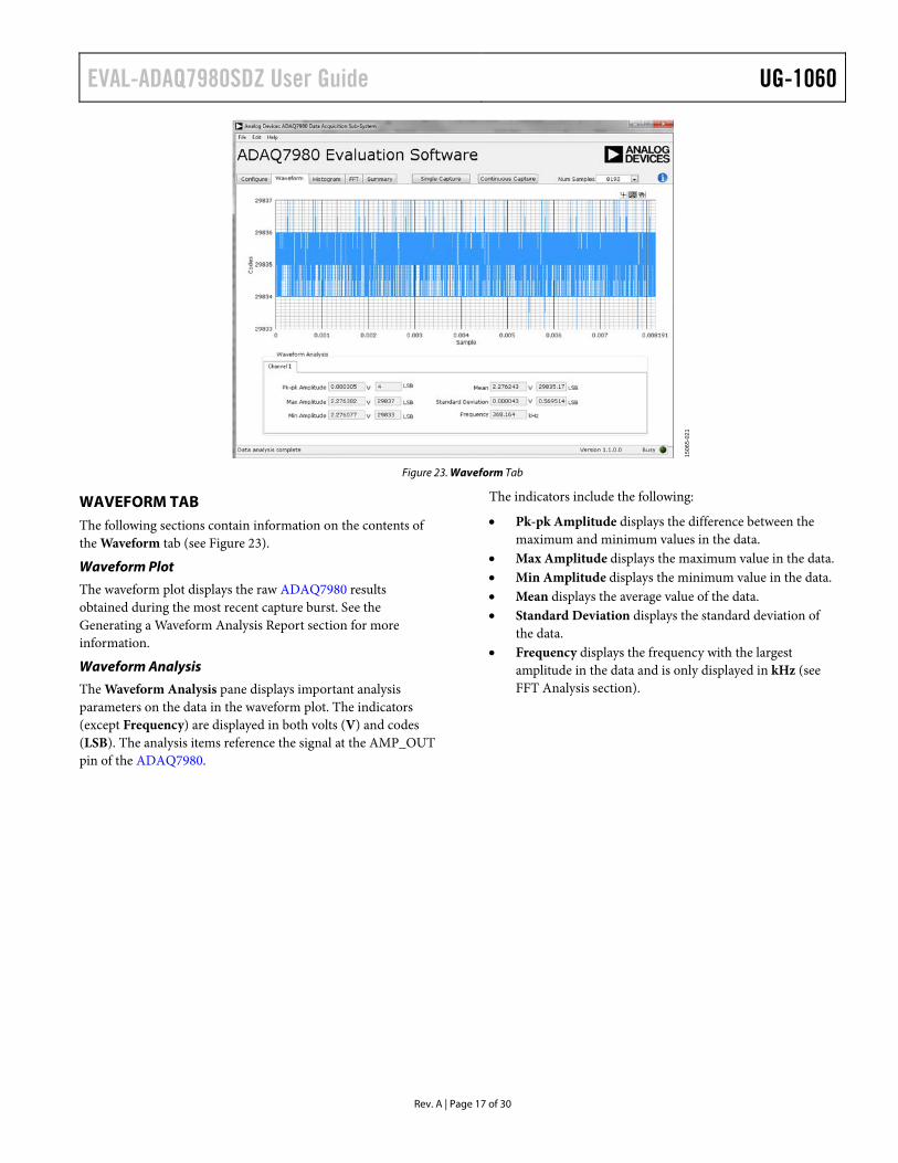
Figure 24. Histogram Tab
HISTOGRAM TAB Histogram Plot
The histogram plot contains a histogram of the results obtained during the most recent capture burst (see Figure 24). This plot shows the number of occurrences for each code in the results. See the Generating a Histogram of the ADC Code Distribution section for more information.
Histogram Analysis
The Histogram Analysis pane displays important analysis parameters on the data in the histogram plot. The indicators are displayed in volts (V) and codes (LSB), unless otherwise specified. The analysis items reference the signal at the AMP_OUT pin of the ADAQ7980.
The parameters include the following:
• Max Amplitude displays the maximum value in the data. • Min Amplitude displays the minimum value in the data. • DC Offset/Mean displays the average value of the data. • Transition Noise (Pk-Pk) displays the peak-to-peak value
of the noise of the signal (displayed in μV and LSB RMS). • Pk-pk Amplitude displays the difference between the
maximum and minimum values in the data. • RMS Noise displays the rms value of the data (displayed
in μV). • LSB displays the equivalent voltage difference between
each code value (displayed in μV). This value is determined by the Reference Voltage (V) control in the Configure tab.
• Histogram Width displays the maximum code in the histogram minus the minimum code in the histogram (displayed in LSB).
1506
5-02
2
EVAL-ADAQ7980SDZ User Guide UG-1060
Rev. A | Page 19 of 30
Figure 25. FFT Tab
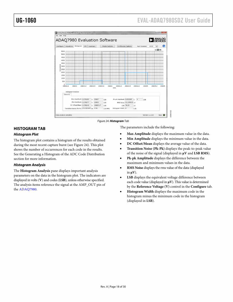
FFT TAB The following contains information on the contents of the FFT tab (see Figure 25).
FFT Plot
The FFT plot displays frequency analysis of the raw ADAQ7980 results from the most recent capture burst. See the Generating an FFT of AC Characteristics section for more information.
FFT Analysis
The FFT Analysis pane displays important ac analysis parameters of the data in the FFT plot. The analysis items reference the signal at the AMP_OUT pin of the ADAQ7980.
The parameters include the following:
• Max Amplitude displays the maximum value in the data (displayed in V and LSB).
• Min Amplitude displays the minimum value in the data (displayed in V and LSB).
• Pk-pk Amplitude displays the difference between the maximum and minimum values in the data (displayed in V and LSB).
• DC displays the average value of the data (displayed in V and LSB).
• Fund. Frequency displays the frequency with the largest amplitude in the FFT (displayed in kHz).
• Fund. Amplitude displays the amplitude of the Fund. Frequency value (displayed in dBFS, which is dB relative to the reference voltage).
• Dynamic Range displays the ratio of a full-scale signal (which is the largest signal the ADAQ7980 can accept with amplitude equal to the reference voltage) to the noise floor value (displayed in dBFS).
• RMS Noise displays the rms voltage of the noise floor in the FFT plot. Specifically, this calculation includes all frequency bins in the FFT plot that are not displayed in the Show Harmonic Content window. This value is used in calculations for Dynamic Range, SNR, SINAD, and SFDR values.
• SNR displays the ratio of the Fund. Amplitude value to the RMS Noise value displayed in dB).
• THD displays the ratio of the energy in second through fifth harmonic frequencies to that of the Fund. Frequency value (displayed in dB).
• SINAD displays the ratio of the Fund. Amplitude value to the RMS Noise value and amplitude of the second through fifth harmonic frequencies (displayed in dB).
• Noise Floor displays the ratio of the RMS Noise value and the full-scale range of the ADAQ7980 set by Reference Voltage in the Configure tab (displayed in dB).
• Bin Width displays the range of frequencies included in each point drawn on the FFT plot. A smaller Bin Width value corresponds with higher resolution in frequency amplitude information in the FFT plot, affected by the Sampling Freq and Num Samples in the Configure tab values. For example, increasing the Num Samples value while leaving Sampling Freq constant results in a smaller Bin Width value.
• SFDR, the spurious-free dynamic range, displays the ratio of the Fund. Amplitude value to the largest spurious frequency amplitude (displayed in dB).
• The Show Harmonic Content button toggles a display showing the Fund. Frequency value and the harmonics amplitudes. Frequencies are displayed in kHz and amplitudes in dBFS.
1506
5-02
3
UG-1060 EVAL-ADAQ7980SDZ User Guide
Rev. A | Page 20 of 30
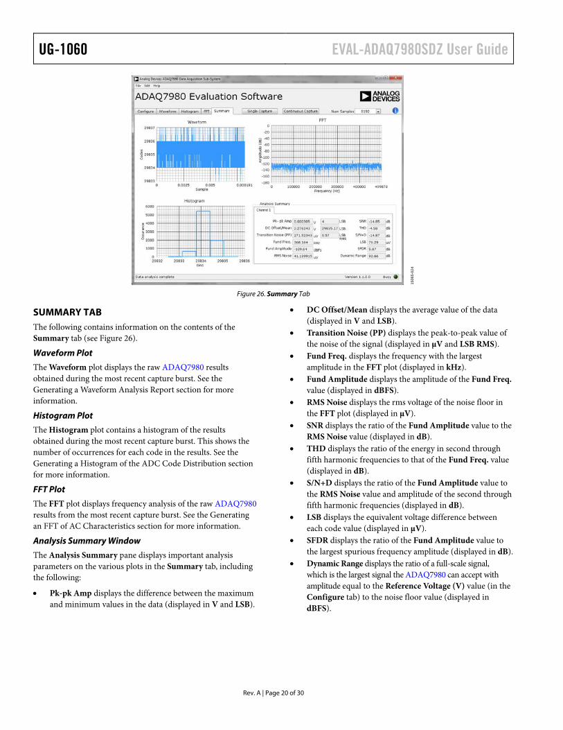
Figure 26. Summary Tab
SUMMARY TAB The following contains information on the contents of the Summary tab (see Figure 26).
Waveform Plot
The Waveform plot displays the raw ADAQ7980 results obtained during the most recent capture burst. See the Generating a Waveform Analysis Report section for more information.
Histogram Plot
The Histogram plot contains a histogram of the results obtained during the most recent capture burst. This shows the number of occurrences for each code in the results. See the Generating a Histogram of the ADC Code Distribution section for more information.
FFT Plot
The FFT plot displays frequency analysis of the raw ADAQ7980 results from the most recent capture burst. See the Generating an FFT of AC Characteristics section for more information.
Analysis Summary Window
The Analysis Summary pane displays important analysis parameters on the various plots in the Summary tab, including the following:
• Pk-pk Amp displays the difference between the maximum and minimum values in the data (displayed in V and LSB).
• DC Offset/Mean displays the average value of the data (displayed in V and LSB).
• Transition Noise (PP) displays the peak-to-peak value of the noise of the signal (displayed in μV and LSB RMS).
• Fund Freq. displays the frequency with the largest amplitude in the FFT plot (displayed in kHz).
• Fund Amplitude displays the amplitude of the Fund Freq. value (displayed in dBFS).
• RMS Noise displays the rms voltage of the noise floor in the FFT plot (displayed in μV).
• SNR displays the ratio of the Fund Amplitude value to the RMS Noise value (displayed in dB).
• THD displays the ratio of the energy in second through fifth harmonic frequencies to that of the Fund Freq. value (displayed in dB).
• S/N+D displays the ratio of the Fund Amplitude value to the RMS Noise value and amplitude of the second through fifth harmonic frequencies (displayed in dB).
• LSB displays the equivalent voltage difference between each code value (displayed in μV).
• SFDR displays the ratio of the Fund Amplitude value to the largest spurious frequency amplitude (displayed in dB).
• Dynamic Range displays the ratio of a full-scale signal, which is the largest signal the ADAQ7980 can accept with amplitude equal to the Reference Voltage (V) value (in the Configure tab) to the noise floor value (displayed in dBFS).
1506
5-02
4
EVAL-ADAQ7980SDZ User Guide UG-1060
Rev. A | Page 21 of 30
EVALUATION HARDWARE AND SOFTWARE OPERATION The following sections outline how to use the ADAQ798x Evaluation Software to capture, analyze and view conversion results from the ADAQ7980.
CAPTURING CONVERSION RESULTS The following describes how to collect conversion results from the EVAL-ADAQ7980SDZ:
1. Set the various controls in the Configure tab to the desired values. See the Configure Tab section for a detailed description of these controls.
2. Once these controls are set, press either the Single Capture or the Continuous Capture buttons in the main window to initial conversions. See the Overview of the Main Window section for more information on these controls.
GENERATING A WAVEFORM ANALYSIS REPORT Figure 23 illustrates the Waveform tab for a dc input signal when using the on-board 5 V external reference.
The Waveform Analysis pane reports the amplitudes recorded from the captured signal and the frequency of the signal tone.
GENERATING A HISTOGRAM OF THE ADC CODE DISTRIBUTION The Histogram tab can perform ac testing or, more commonly, dc testing. This tab shows the ADC code distribution of the input and computes the mean and standard deviation, which are displayed as DC Offset/Mean and Transition Noise (Pk-Pk), respectively, in the Histogram Analysis pane.
Figure 24 shows the histogram of a dc signal applied to the ADC input along with the resulting calculations.
AC Input
To perform a histogram test of ac input,
1. Apply a sinusoidal signal with low distortion (better than 100 dB) to the evaluation board at the P1/P2 input SMA connector pair.
2. Click the Histogram tab from the main window. 3. Click the Single Capture or Continuous Capture button.
Raw data is then captured and passed to the PC for statistical computations, and various measured values are displayed in the Histogram Analysis pane.
DC Input
To perform a histogram test of dc input,
1. If using an external source, apply a signal to the evaluation board at the P1/P2 input SMA connector pair. It can be required to filter the signal to ensure that the dc source is noise compatible with the ADC.
2. Click the Histogram tab from the main window. 3. Click the Single Capture or Continuous Capture button.
Raw data is then captured and passed to the PC for statistical computations, and various measured values are displayed in the Histogram Analysis pane.
GENERATING AN FFT OF AC CHARACTERISTICS Figure 25 shows the FFT tab. This feature tests the traditional ac characteristics of the ADC and displays an FFT plot of the results.
To perform an ac FFT test,
1. Apply a sinusoidal signal with low distortion (better than 100 dB) to the evaluation board at the P1/P2 input SMA connector pair. To attain the requisite low distortion, which is necessary to allow true evaluation of the ADAQ7980, one option is to a. Filter the input signal from the ac source. A band-pass
filter can be used; its center frequency must match the test frequency of interest.
b. If using a low frequency band-pass filter when the full-scale input range is more than a few volts peak-to-peak, use the on-board amplifiers to amplify the signal, thus preventing the filter from distorting the input signal.
2. Click the FFT tab from the main window. 3. Click the Single Capture button or Continuous Capture
button.
As in the histogram test, raw data is then captured and passed to the PC, which performs the FFT and displays the resulting signal-to-noise ratio (SNR), signal-to-noise-and-distortion ratio (SINAD), total harmonic distortion (THD), and spurious-free dynamic range (SFDR).
The FFT Analysis pane displays the results of the captured data.
UG-1060 EVAL-ADAQ7980SDZ User Guide
Rev. A | Page 22 of 30
GENERATING A SUMMARY OF THE WAVEFORM, HISTOGRAM, AND FAST FOURIER TRANSFORM Figure 26 shows the Summary tab. The Summary tab captures all the display information and provides it in one pane with a synopsis of the information, including key performance parameters such as SNR and THD.
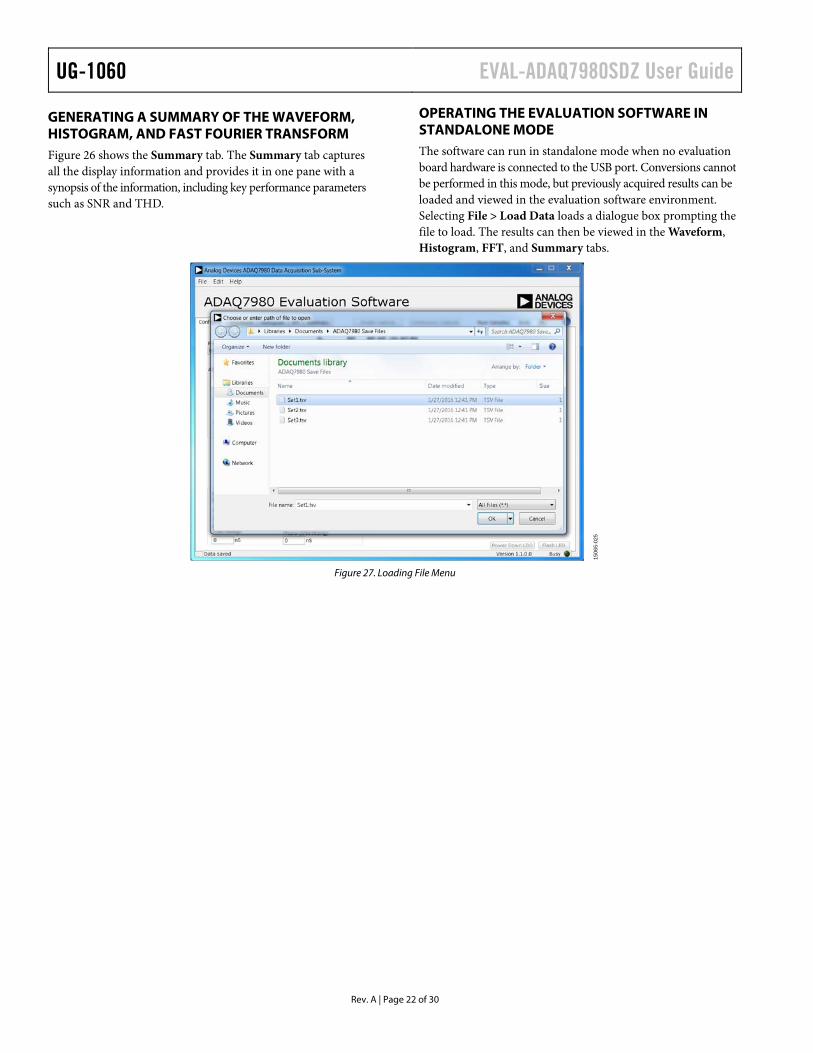
OPERATING THE EVALUATION SOFTWARE IN STANDALONE MODE The software can run in standalone mode when no evaluation board hardware is connected to the USB port. Conversions cannot be performed in this mode, but previously acquired results can be loaded and viewed in the evaluation software environment. Selecting File > Load Data loads a dialogue box prompting the file to load. The results can then be viewed in the Waveform, Histogram, FFT, and Summary tabs.
Figure 27. Loading File Menu
1506
5-02
5
EVAL-ADAQ7980SDZ User Guide UG-1060
Rev. A | Page 23 of 30
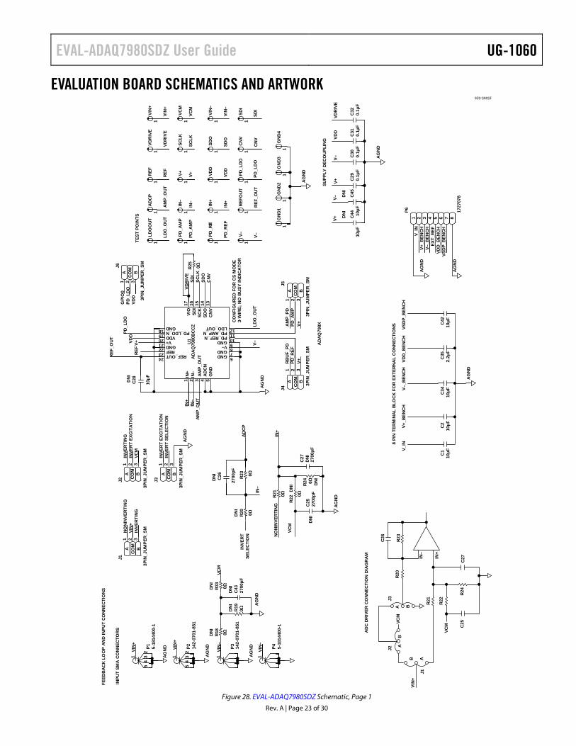
EVALUATION BOARD SCHEMATICS AND ARTWORK
Figure 28. EVAL-ADAQ7980SDZ Schematic, Page 1
INPU
T SM
A C
ON
NEC
TOR
S
TEST
PO
INTS
SUPP
LY D
ECO
UPL
ING
AD
C D
RIV
ER C
ON
NEC
TIO
N D
IAG
RA
M
CO
NFI
GU
RED
FO
R C
S M
OD
E3-
WIR
E; N
O B
USY
IND
ICA
TOR
AD
AQ
798X
8 PI
N T
ERM
INA
L B
LOC
K F
OR
EXT
ERN
AL
CO
NN
ECTI
ON
S
FEED
BA
CK
LO
OP
AN
D IN
PUT
CO
NN
ECTI
ON
S
3PIN
_JU
MPE
R_S
M
3PIN
_JU
MPE
R_S
M3P
IN_J
UM
PER
_SM
142-
0701
-851
DN
I0Ω
2700
pF14
2-07
01-8
51
0ΩD
NI
DN
I
0Ω
3PIN
_JU
MPE
R_S
M
DN
I
AD
AQ
7980
BC
CZ
10µF
DN
I
3PIN
_JU
MPE
R_S
M
DN
ID
NI
10µF
10µF
10µF
10µF
5-18
1440
0-1
2700
pF
DN
I
5-18
1440
0-1
0.1µ
F
1727
078
3PIN
_JU
MPE
R_S
M
0Ω
0Ω
10µF
0.1µ
F
DN
I
0Ω
0Ω
0Ω27
00pF
DN
ID
NI
DN
I27
00pF
DN
I
0Ω
0.1µ
F
10µF
2.2µ
F
0.1µ
FC
44C
45
C43R
33
SDI
C42
C35
C34
C2
C1
P6
U1
J3J2J1
J6
J5J4
R25
GN
D2
GN
D4
GN
D3
GN
D1
VIN
–
VCM
VIN
+
V–R
EFO
UT
PD_L
DO
CN
V
PD_R
E FIN
+VD
DSD
O
PD_A
MP
IN–
V+SC
LK
VDR
IVE
REF
AD
CP
LDO
OU
T
C32
C31
C30
C29
C28
C26 R23
R20
P4P1
R19
R18
P3P2
C25R
22
R24
C27
R21
LDO
_OU
T
VCM
INVE
RT
SELE
CTI
ON
INVE
RTI
NG
VIN
+N
ON
INVE
RTI
NG
VCM
INVE
RT
EXC
ITA
TIO
NIN
VER
T SE
LEC
TIO
N
VIN
+
IN+
IN–
VCM
VIN
–
RB
UF_
PD
V–
VDR
IVE
SDI
SCLK
SDO
AM
P_O
UT
INVE
RT
EXC
ITA
TIO
N
IN+
V+
PD_R
EF
CN
V
INVE
RTI
NG
SCLK
VDD
IN+
LDO
_OU
T
PD_A
MP
PD_R
EF
VDR
IVE
VIN
–
REF
SDO
V–
VIN
–
VDR
IVE
V–
EXT_
REF
VDD
_BEN
CH
VSD
P_B
ENC
H
V+_B
ENC
HV–
_BEN
CH
NO
NIN
VER
TIN
G
VIN
+
SDI
V–_B
ENC
HVS
DP_
BEN
CH
AM
P_PD
V_IN
VDD
PD_L
DO
V+_B
ENC
H
V_IN
IN–
V+
AM
P_O
UT
AD
CP
V+
GPI
O0
VIN
+
REF
_OU
T
PD_A
MP
CN
V
VCM
V+
PD_L
DO
REF
_OU
T
IN–
PD_L
DO
VDD
V+R
EF
VDD
_BEN
CH
V+V–
VDD
1
87654321
1019 11
2117
20
821
1416 15
2423
12
22
18
9
76
513
3 4
2 312 312 31
2 31
2 312 31
11
11
111
11
11
11
11
11
111
11
1
1
23
45
23
45
1 11
AG
ND
AG
ND
AG
ND
AG
ND
AG
ND
AG
ND
AG
ND
AG
ND
VCM
VCM C25
C27
R24
R21
IN–
IN+
R20
C26
R23
R22
J1
VIN
+
J2
A
AA
BB
B
J3
AG
ND
AG
ND
AG
ND
REF_OUTREFGND
V+VDD
PD_LDO_NGND
VIO
SDI
SCK
SDO
CN
V
LDO_OUTPD_AMP_NPD_REF_NGNDV–GNDGND
GN
DA
DC
NA
MP_
OU
TIN
–IN
+
BC
OMAB
CO
MA
BC
OMA
BC
OMA
BC
OMA
BC
OMA
AG
ND
15065-026
UG-1060 EVAL-ADAQ7980SDZ User Guide
Rev. A | Page 24 of 30
Figure 29. EVAL-ADAQ7980SDZ Schematic, Page 2
VIO: USE TO SET IO VOLTAGE,MAX DRAW 20mA
INTERFACE GLUE LOGIC
DECOUPLING FOR INTERFACE GLUE LOGIC
SDP CONNECTOR
100kΩ
100kΩ
DNI
100kΩ
FX8-120S-SV(21)
NC7S08P5X
NC7S08P5X
24LC32A-I/MC
0.1µF 0.1µF0.1µF 0.1µF
100kΩ
R29
C38 C39 C40 C41
U11NC7S04M5X
U14NC7S08P5X
U13
U12
P8R30
R32
U10R31
VDRIVE
SPORT_RSCLK
GPIO5
CNVSPORT_DT0
SPORT_RFSSDO
GPIO0GPIO2
SDP_3.3V
V_SDP
SPORT_TSCLK
CNV
SPORT_RFS
SPORT_RSCLK
SCLK
VDRIVE
VDRIVE VDRIVE
SPORT_TSCLK
GPIO7
REF_PDRBUF_PD
GPIO3GPIO1
GPIO4
AMP_PDGPIO6
SDP_3.3V
SDP_3.3V
VDRIVE
VDRIVE
SDP_3.3V
4
5
1 3
2 4
5
3
21
4
5
3
21
4
5
3
21
65
116
1
5
6259
72497348
87
89
3029 92
9032
88
3191
3837
85
39
8483
3433
82
64
35
41 8042 79
57
60
1002199
26 9527
7 1148 1139 112
10 111110
1213 10814 10715 10616 105
18 10319 10220 101
22
94
24 9725 96
120119
70
68676655
5453
5150
2
7447
764577447843
118117
115
109
104
98
93
86
81
75
69
6358
52
46
40
36
28
23
17
11
6
43
56
71
61
7
4
8
56
PAD
321
SPI_SEL_A
CLKOUT
NCNC
GNDGND
VIO(+3.3V)GND
PAR_D22PAR_D20PAR_D18PAR_D16PAR_D15
GNDPAR_D12PAR_D10
PAR_D8PAR_D6
GNDPAR_D4PAR_D2PAR_D0
PAR_WR_NPAR_INT
GNDPAR_A2PAR_A0
PAR_FS2PAR_CLK
GNDSPORT_RSCLK
SPORT_DR0SPORT_RFSSPORT_TFSSPORT_DT0
SPORT_TSCLKGND
SPI_MOSISPI_MISOSPI_CLK
GNDSDA_0SCL_0GPIO1GPIO3GPIO5
GNDGPIO7
TMR_BTMR_D
NCGND
NCNCNC
WAKE_NSLEEP_N
GNDUART_TXBMODE1RESET_IN_N
UART_RXGNDRESET_OUT_NEEPROM_A0NCNCNCGNDNCNCTMR_CTMR_AGPIO6GNDGPIO4GPIO2GPIO0SCL_1SDA_1GNDSPI_SEL1/SPI_SS_NSPI_SEL_C_NSPI_SEL_B_NGNDSERIAL_INTSPI_D3SPI_D2SPORT_DT1SPORT_DR1SPORT_TDV1SPORT_TDV0GNDPAR_FS1PAR_FS3PAR_A1PAR_A3GNDPAR_CS_NPAR_RD_NPAR_D1PAR_D3PAR_D5GNDPAR_D7PAR_D9PAR_D11PAR_D13PAR_D14GNDPAR_D17PAR_D19PAR_D21PAR_D23GNDUSB_VBUSGNDGNDNCVIN
AGND
AGNDAGND
PAD
VCCWP
SCLSDAVSS
A2A1A0
AGND
VCC
Y
GND NC
A
VCC
Y
GNDBA
AGND
VCC
Y
GNDBA
AGND
AGND
VCC
Y
GNDBA
AGND
AGND
a
1506
5-03
0
EVAL-ADAQ7980SDZ User Guide UG-1060
Rev. A | Page 25 of 30
Figure 30. EVAL-ADAQ7980SDZ Schematic, Page 3
VCM SOURCE
VCM SMB CONNECTOR
5 VOLTS
ON-BOARD/BENCH
REFERENCE SOURCES
3.3 VOLTS
DNI
0Ω
0.1µF
M20-9990345
3PIN_JUMPER_SM
ADR3433ARJZ
2700PF10µF
0Ω
DNI
ADR4550BRZ
DNI
0Ω
2700pF
10µF
0Ω
0.1µF
10kΩ
10kΩ
0.1µF
0Ω
0
0Ω
3PIN_JUMPER_SM
0.1µF
M20-9990345
10µF0.1µF
10µF
10µF
SMB1251B1-3GT30G-50
ADA4805-1ARJZ
3PIN_JUMPER_SM
J20
J8
J7
P5R17
C24
R16
C22
U4R15
C23
R14
C20
J10
C21
C18
R13
C17
R11
J9
R12
C19
U2
C16C15
R10
U3
C14C13
R9
EXT_REF
ON_BOARD_REFREF
REF_PD
3P3V_REF
5V_REF
REF
V+
ONBOARD_7P5V
ONBOARD_5V
V+
ON_BOARD_REF
VCM
23
1
23
1
23
1
5 4 3 2
11
52
4
6
3
321
321
62
8
75314
AGND
VOUT_FORCEVOUT_SENSE
VINENABLE
GND_SENSEGND_FORCE
AGND
BCOMA
BCOMA
BCOMA
AGND
AGND
AGND
AGND
+VS
–VSDIS_N
–IN
+INVOUT
AGND
AGND
AGND
AGND
AGND
AGND
NC1
VIN
GNDTP
VOUT
1506
5-02
7
UG-1060 EVAL-ADAQ7980SDZ User Guide
Rev. A | Page 26 of 30
Figure 31. EVAL-ADAQ7980SDZ Schematic, Page 4
Figure 32. EVAL-ADAQ7980SDZ Schematic, Page 5
VDRIVE SUPPLY
SDP SUPPLY
VDD SUPPLY
IF SUPPLYING FROM VSDP_BENCH (P2 = 3), VSDP_BENC NEEDS TO BE LIMITED TO 5V MAX
DNI
DNIDNI
M20-9990345
M20-9990345
0Ω
2.2µF
2700pF
0Ω
0Ω2.2µF
ADP7118AUJZ-3.3
M20-9990345
M20-9990345
J12 C33
R26
U5
R27
C36
C37
R28
J14
J13
J11
V_SDPONBOARD_5V
SDP_3P3VVDRIVE
V_IN
VDD_BENCH
VSDP_BENCH
VDDONBOARD_VDD
ONBOARD_VDDONBOARD_7P5V
ONBOARD_5V
321
51
4
2
3
321
321
321
AGND
AGND
AGND
VOUTSENSE/ADJEN
GND
VIN
AGND
1506
5-02
8
VIN = +9V, VOUT = 7.5V
DC POWER JACK
VIN = +9V, VOUT = -2.5V
POWER SUPPLY FOR AMPLIFIERS
ON-BOARD / BENCH
UNIPOLAR / BIPOLAR
ON-BOARD
ON-BOARD / BENCH
KLDX-SMT2-0202-ATR
2.4kΩ
0kΩ
ADP7118AUJZ-5.0
10µF
10µF
ADP2370ACPZ-5.0
0Ω10µF10µF
0Ω
ADM660ARZ10µH
10µF
DNISML-310MTT86
ADP7182AUJZ
2.2µF
100kΩ
2.2µF
1µF
M20-9990345
M20-9990345
1kΩ AT 100MHz
10µF
3PIN_JUMPER_SM
1kΩ
M20-9990345
0Ω
M20-9990345
50kΩ
10µFDNI
DNI
C12
C11
R8
U9
C8
C10
C9
U8C3C7
R6
R3
R5J15
U6
L2
J17
J19
C5
R4
J16
R2
R7
C6C4
J18
L1
R1P7
U7
DS1
V-_BENCH
FSEL
ONBOARD_5V
EXT_V-ONBOARD_M2P5V
ONBOARD_V+
ONBOARD_5VONBOARD_V+
EXT_V-
ONBOARD_7P5V
FSEL
V_IN
V-
V+V+_BENCH
ONBOARD_M2.5V5
2
1
3
4
8
5
7
6 3
1
42
23
1
1
4
78
62
5
PAD
3
2 1
321
321
321
321
4321
51
4
2
3
A
C
AGND
AGND
AGND
AGNDAGND
VIN
EN
GNDADJ
VOUT
AGND
AGND
V+OSC
LV
OUTCAP–
GND
CAP+FC
AGND
BCOM
A
EPAD
PGNDSWPGFBSYNC
ENFSELVIN
AGND
AGND
AGND
VOUTSENSE/ADJEN
GND
VIN
AGND
AGNDAGND
1506
5-02
9
EVAL-ADAQ7980SDZ User Guide UG-1060
Rev. A | Page 27 of 30
1506
5-03
1
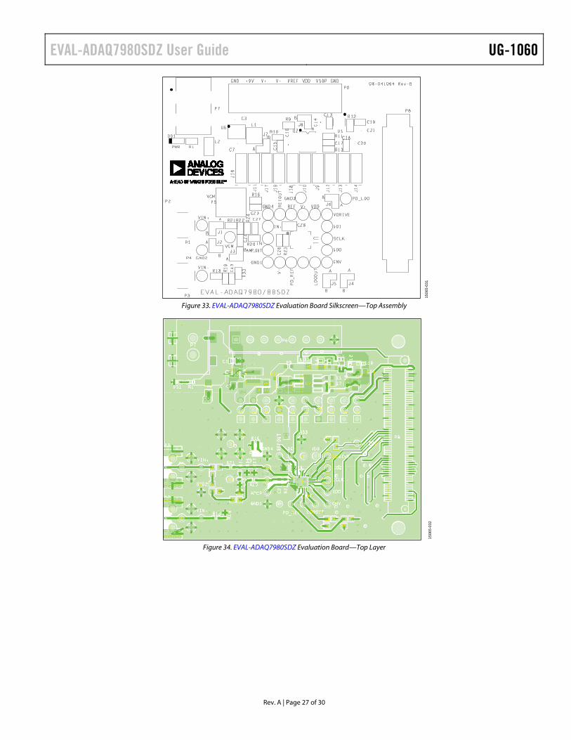
Figure 33. EVAL-ADAQ7980SDZ Evaluation Board Silkscreen—Top Assembly
1506
5-03
2
Figure 34. EVAL-ADAQ7980SDZ Evaluation Board—Top Layer
UG-1060 EVAL-ADAQ7980SDZ User Guide
Rev. A | Page 28 of 30
1506
5-03
3
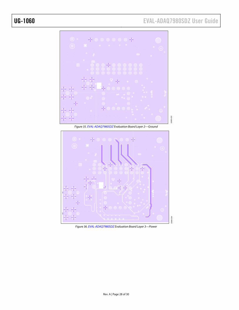
Figure 35. EVAL-ADAQ7980SDZ Evaluation Board Layer 2—Ground
1506
5-03
4
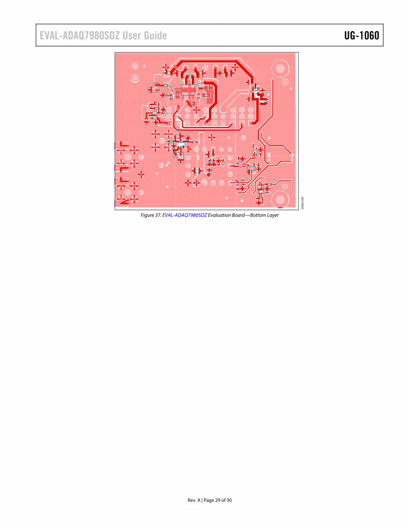
Figure 36. EVAL-ADAQ7980SDZ Evaluation Board Layer 3—Power
EVAL-ADAQ7980SDZ User Guide UG-1060
Rev. A | Page 29 of 30
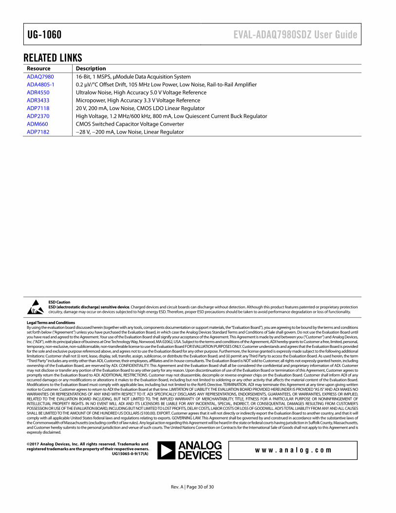
Figure 37. EVAL-ADAQ7980SDZ Evaluation Board—Bottom Layer
1506
5-03
5
UG-1060 EVAL-ADAQ7980SDZ User Guide
Rev. A | Page 30 of 30
RELATED LINKS Resource Description ADAQ7980 16-Bit, 1 MSPS, μModule Data Acquisition System ADA4805-1 0.2 µV/°C Offset Drift, 105 MHz Low Power, Low Noise, Rail-to-Rail Amplifier ADR4550 Ultralow Noise, High Accuracy 5.0 V Voltage Reference ADR3433 Micropower, High Accuracy 3.3 V Voltage Reference ADP7118 20 V, 200 mA, Low Noise, CMOS LDO Linear Regulator ADP2370 High Voltage, 1.2 MHz/600 kHz, 800 mA, Low Quiescent Current Buck Regulator ADM660 CMOS Switched Capacitor Voltage Converter ADP7182 −28 V, −200 mA, Low Noise, Linear Regulator
ESD Caution ESD (electrostatic discharge) sensitive device. Charged devices and circuit boards can discharge without detection. Although this product features patented or proprietary protection circuitry, damage may occur on devices subjected to high energy ESD. Therefore, proper ESD precautions should be taken to avoid performance degradation or loss of functionality.
Legal Terms and Conditions By using the evaluation board discussed herein (together with any tools, components documentation or support materials, the “Evaluation Board”), you are agreeing to be bound by the terms and conditions set forth below (“Agreement”) unless you have purchased the Evaluation Board, in which case the Analog Devices Standard Terms and Conditions of Sale shall govern. Do not use the Evaluation Board until you have read and agreed to the Agreement. Your use of the Evaluation Board shall signify your acceptance of the Agreement. This Agreement is made by and between you (“Customer”) and Analog Devices, Inc. (“ADI”), with its principal place of business at One Technology Way, Norwood, MA 02062, USA. Subject to the terms and conditions of the Agreement, ADI hereby grants to Customer a free, limited, personal, temporary, non-exclusive, non-sublicensable, non-transferable license to use the Evaluation Board FOR EVALUATION PURPOSES ONLY. Customer understands and agrees that the Evaluation Board is provided for the sole and exclusive purpose referenced above, and agrees not to use the Evaluation Board for any other purpose. Furthermore, the license granted is expressly made subject to the following additional limitations: Customer shall not (i) rent, lease, display, sell, transfer, assign, sublicense, or distribute the Evaluation Board; and (ii) permit any Third Party to access the Evaluation Board. As used herein, the term “Third Party” includes any entity other than ADI, Customer, their employees, affiliates and in-house consultants. The Evaluation Board is NOT sold to Customer; all rights not expressly granted herein, including ownership of the Evaluation Board, are reserved by ADI. CONFIDENTIALITY. This Agreement and the Evaluation Board shall all be considered the confidential and proprietary information of ADI. Customer may not disclose or transfer any portion of the Evaluation Board to any other party for any reason. Upon discontinuation of use of the Evaluation Board or termination of this Agreement, Customer agrees to promptly return the Evaluation Board to ADI. ADDITIONAL RESTRICTIONS. Customer may not disassemble, decompile or reverse engineer chips on the Evaluation Board. Customer shall inform ADI of any occurred damages or any modifications or alterations it makes to the Evaluation Board, including but not limited to soldering or any other activity that affects the material content of the Evaluation Board. Modifications to the Evaluation Board must comply with applicable law, including but not limited to the RoHS Directive. TERMINATION. ADI may terminate this Agreement at any time upon giving written notice to Customer. Customer agrees to return to ADI the Evaluation Board at that time. LIMITATION OF LIABILITY. THE EVALUATION BOARD PROVIDED HEREUNDER IS PROVIDED “AS IS” AND ADI MAKES NO WARRANTIES OR REPRESENTATIONS OF ANY KIND WITH RESPECT TO IT. ADI SPECIFICALLY DISCLAIMS ANY REPRESENTATIONS, ENDORSEMENTS, GUARANTEES, OR WARRANTIES, EXPRESS OR IMPLIED, RELATED TO THE EVALUATION BOARD INCLUDING, BUT NOT LIMITED TO, THE IMPLIED WARRANTY OF MERCHANTABILITY, TITLE, FITNESS FOR A PARTICULAR PURPOSE OR NONINFRINGEMENT OF INTELLECTUAL PROPERTY RIGHTS. IN NO EVENT WILL ADI AND ITS LICENSORS BE LIABLE FOR ANY INCIDENTAL, SPECIAL, INDIRECT, OR CONSEQUENTIAL DAMAGES RESULTING FROM CUSTOMER’S POSSESSION OR USE OF THE EVALUATION BOARD, INCLUDING BUT NOT LIMITED TO LOST PROFITS, DELAY COSTS, LABOR COSTS OR LOSS OF GOODWILL. ADI’S TOTAL LIABILITY FROM ANY AND ALL CAUSES SHALL BE LIMITED TO THE AMOUNT OF ONE HUNDRED US DOLLARS ($100.00). EXPORT. Customer agrees that it will not directly or indirectly export the Evaluation Board to another country, and that it will comply with all applicable United States federal laws and regulations relating to exports. GOVERNING LAW. This Agreement shall be governed by and construed in accordance with the substantive laws of the Commonwealth of Massachusetts (excluding conflict of law rules). Any legal action regarding this Agreement will be heard in the state or federal courts having jurisdiction in Suffolk County, Massachusetts, and Customer hereby submits to the personal jurisdiction and venue of such courts. The United Nations Convention on Contracts for the International Sale of Goods shall not apply to this Agreement and is expressly disclaimed.
©2017 Analog Devices, Inc. All rights reserved. Trademarks and registered trademarks are the property of their respective owners. UG15065-0-9/17(A)
Top Related