


γλώσσες
Σελίδες
Νομικός

RESEARCH FRONT
CSIRO PUBLISHINGReview
Aust. J. Chem. 2007, 60, 472–483 www.publish.csiro.au/journals/ajc
Electrochemical Sensors Based on Architectural Diversityof the π-Conjugated Structure: Recent Advancementsfrom Conducting Polymers and Carbon Nanotubes
Liming DaiA
ADepartment of Chemical and Materials Engineering, Department of Chemistry, and UDRI,University of Dayton, Dayton, OH 45469-0240, USA. Email: [email protected]
Conjugated conducting polymers and carbon nanotubes, both of which possess a conjugated structure of alternatingcarbon–carbon single and double bonds for the delocalization of π-electrons, are two important classes of electrochemicalsensing materials. The combination of carbon nanotubes with conducting polymers or other functional materials (e.g.,DNA chains, proteins, metal nanoparticles, carbon fibres) was found to create synergetic effects, that provide the basis forthe development of numerous novel sensors with a high sensitivity, good selectivity, excellent environmental stability, andlow power consumption. This article reviews recent developments in this exciting new area of electrochemical sensingby presenting the rational strategy of the author’s group in the design and characterization of these new electrochemicalsensors based on architectural diversity of the π-conjugated structure.
Manuscript received: 13 December 2006.Final version: 4 April 2007.
The recent development of nanotechnology has opened up novelfundamental and applied frontiers in materials science andengineering.[1] At the nanometer scale, the wave-like propertiesof electrons inside matter and atomic interactions are influencedby the size of the material.[2] As a consequence, changes in thesize-dependent properties (e.g., melting points and magnetic,optic, and electronic properties) may be observed even withoutany compositional change.[2] Due to the high surface-to-volumeratio associated with nanometer-sized materials, a tremendousimprovement in chemical properties is also achievable througha reduction in size.[2] Furthermore, new phenomena, such as theconfinement-induced quantization effect, could also occur whenthe size of materials becomes comparable to the de Broglie wave-length of charge carriers inside.[2] By creating nanostructures,therefore, it is possible to control the fundamental properties ofmaterials through the surface/size effect. This should, in princi-ple, allow us to develop new materials and advanced devices ofdesirable properties and functions for numerous applications.
Polymers offer a class of materials in which the natural lengthof polymer chains and their morphologies in the bulk lie pre-cisely in the nanometer length scale.[2] This, together with thelarge number of possible configurations/conformations availableto a macromolecular chain, indicates a considerable space for
Dr Liming Dai joined the University of Dayton in 2004 as theWright Brothers Institute Endowed Chair Professor of Nanomaterials.He received his Ph.D. in chemistry from the Australian National University in 1990 under the supervision of Professor John W.White. He accepted a postdoctoral fellowship in physics from the Cavendish Laboratory at the University of Cambridge, and avisiting fellowship from the Department of Materials Science and Engineering at the University of Illinois. Thereafter, Dai spent10 years with CSIRO in Australia. Dr Dai’s expertise lies across several fields, including the synthesis, chemical modification, anddevice fabrication of conjugated polymers, fullerene-containing polymers, and carbon nanotubes, with nearly 200 publicationsand several mongraphs. He has received several awards including the 2006 Sigma Xi’s George Noland Research Award, and the2006 Outstanding Engineers and Scientists Award from the Affiliate Societies Council of Dayton.
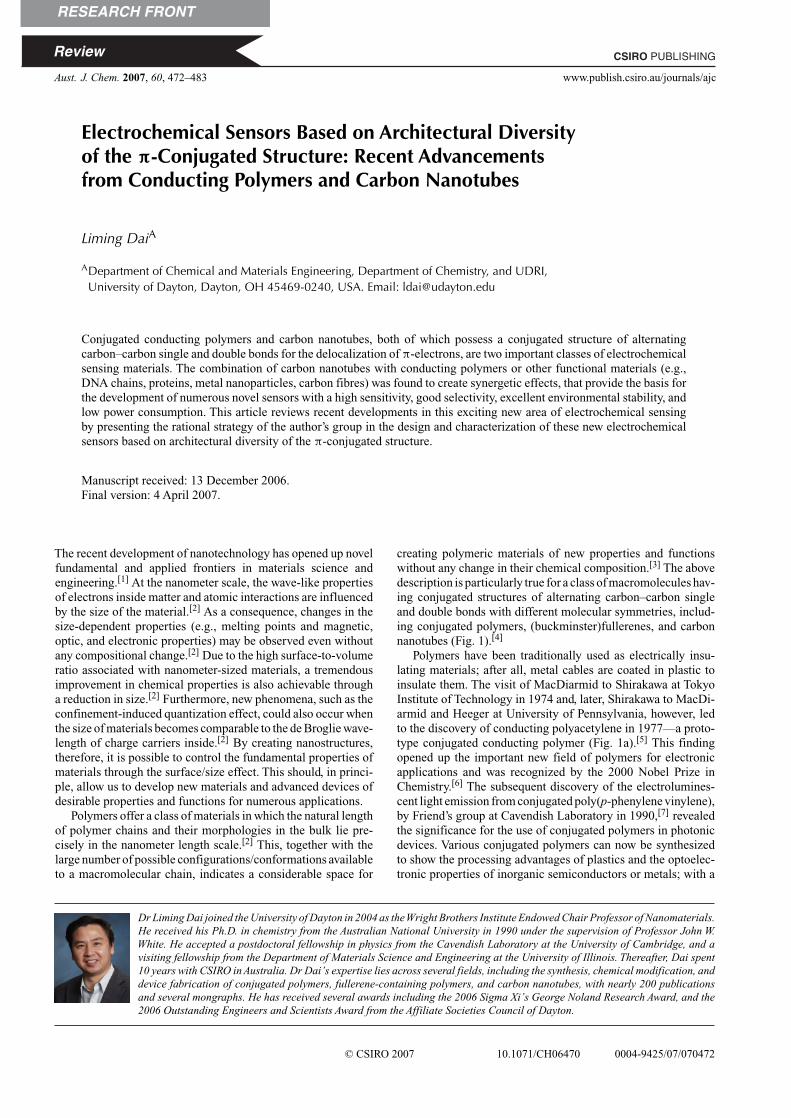
creating polymeric materials of new properties and functionswithout any change in their chemical composition.[3] The abovedescription is particularly true for a class of macromolecules hav-ing conjugated structures of alternating carbon–carbon singleand double bonds with different molecular symmetries, includ-ing conjugated polymers, (buckminster)fullerenes, and carbonnanotubes (Fig. 1).[4]
Polymers have been traditionally used as electrically insu-lating materials; after all, metal cables are coated in plastic toinsulate them. The visit of MacDiarmid to Shirakawa at TokyoInstitute of Technology in 1974 and, later, Shirakawa to MacDi-armid and Heeger at University of Pennsylvania, however, ledto the discovery of conducting polyacetylene in 1977—a proto-type conjugated conducting polymer (Fig. 1a).[5] This findingopened up the important new field of polymers for electronicapplications and was recognized by the 2000 Nobel Prize inChemistry.[6] The subsequent discovery of the electrolumines-cent light emission from conjugated poly(p-phenylene vinylene),by Friend’s group at Cavendish Laboratory in 1990,[7] revealedthe significance for the use of conjugated polymers in photonicdevices. Various conjugated polymers can now be synthesizedto show the processing advantages of plastics and the optoelec-tronic properties of inorganic semiconductors or metals; with a
© CSIRO 2007 10.1071/CH06470 0004-9425/07/070472
RESEARCH FRONT
Electrochemical Sensors 473
CH
CH
CH
CH
CH
CH
CH
CH
CH
CH
CH
CH
(a)
(b)
Graphenesheet(s)
Roll-up
(c)
Fig. 1. Conjugated structures with different dimensionalities: (a) polyacetylene, (b) buckminsterfullereneC60, (c) single- and double-wall carbon nanotubes.
Table 1. Some conjugated conducting polymers[4]
Polymer (date conductivity discovered) Structure π–π∗ gap [eV] ConductivityA [S cm−1]
Polyacetylene and analoguesPolyacetylene (1977) 1.5 103–1.7 × 10⁵
n
Polypyrrole (1979) 3.1 102–7.5 × 10³
N
H
n
Polythiophene (1981) 2.0 10–103S
n
Polyphenylene and analoguesPoly(paraphenylene) (1979) 3.0 102–103
n
Poly(p-phenylene vinylene) (1979) 2.5 3–5 × 10³
n
Polyaniline (1980) 3.2 30–200NH
NH
N N
X1�X
AThe range of conductivities listed is from that originally found to the highest values obtained to date.
conductivity even up to 1.7 × 10⁵ S cm−1 comparing favourablywith the value of 106 S cm−1 for copper or silver[8] (Table 1).
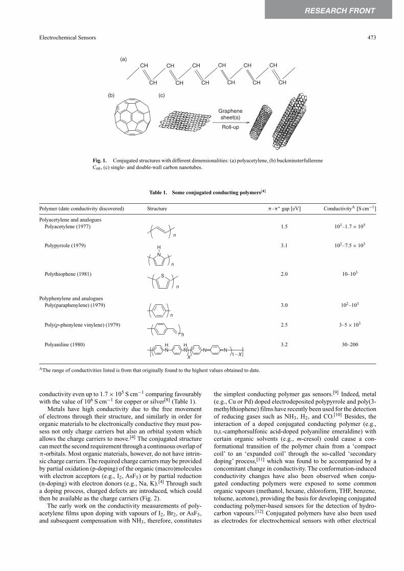
Metals have high conductivity due to the free movementof electrons through their structure, and similarly in order fororganic materials to be electronically conductive they must pos-sess not only charge carriers but also an orbital system whichallows the charge carriers to move.[4] The conjugated structurecan meet the second requirement through a continuous overlap ofπ-orbitals. Most organic materials, however, do not have intrin-sic charge carriers. The required charge carriers may be providedby partial oxidation (p-doping) of the organic (macro)moleculeswith electron acceptors (e.g., I2, AsF5) or by partial reduction(n-doping) with electron donors (e.g., Na, K).[4] Through sucha doping process, charged defects are introduced, which couldthen be available as the charge carriers (Fig. 2).
The early work on the conductivity measurements of poly-acetylene films upon doping with vapours of I2, Br2, or AsF5,and subsequent compensation with NH3, therefore, constitutes
the simplest conducting polymer gas sensors.[9] Indeed, metal(e.g., Cu or Pd) doped electrodeposited polypyrrole and poly(3-methylthiophene) films have recently been used for the detectionof reducing gases such as NH3, H2, and CO.[10] Besides, theinteraction of a doped conjugated conducting polymer (e.g.,d,l-camphorsulfonic acid-doped polyaniline emeraldine) withcertain organic solvents (e.g., m-cresol) could cause a con-formational transition of the polymer chain from a ‘compactcoil’ to an ‘expanded coil’ through the so-called ‘secondarydoping’ process,[11] which was found to be accompanied by aconcomitant change in conductivity. The conformation-inducedconductivity changes have also been observed when conju-gated conducting polymers were exposed to some commonorganic vapours (methanol, hexane, chloroform, THF, benzene,toluene, acetone), providing the basis for developing conjugatedconducting polymer-based sensors for the detection of hydro-carbon vapours.[12] Conjugated polymers have also been usedas electrodes for electrochemical sensors with other electrical
RESEARCH FRONT
474 L. Dai
�
�
��
�
�
�
��e
�e
�e
�e
(a) (b)
Fig. 2. A schematic description of the doping of trans-polyacetylene chain: (a) p-doping and (b) n-doping.
transducers, including potentiometry, amperometry, and voltam-metry. The fundamental principle and the advantages and disad-vantages for each of the electrical transduction modes have beenreviewed elsewhere.[4]
Sometimes history repeats itself. The visit made by Kroto in1985 to Smalley and Curl at Rice University led also to a NoblePrize winning discovery of buckminsterfullerene C60—a conju-gated molecule with a soccer-ball like structure consisting of 12pentagons and 20 hexagons facing symmetrically (Fig. 1b).[13]
Although Osawa[14] had theoretically predicted the structureof C60 in 1970 and Huffman[15] might have produced the C60molecules in his ‘graphite smoke’ as early as 1973, it was the1985 discovery that generated a great deal of interest and createdan entirely new branch of carbon chemistry.[16] The subsequentdiscovery of carbon nanotubes (CNTs) by Iijima[17] in 1991opened up a new era in material science and nanotechnology.[1]
Carbon nanotubes (CNTs, Fig. 1c) may be viewed as a graphitesheet that is rolled up into a nanoscale tube form (single-walledcarbon nanotubes, SWNTs) or with additional graphene tubesaround the core of a SWNT (multi-walled carbon nanotubes,MWNTs).[1]
In view of the large number of well defined carbon–carbonsingle- and double-bonds in their molecular structure, fullerenesand carbon nanotube are polymeric in essence. Just as conjugatedpolymers have widely been regarded as quasi one-dimensionalsemiconductors,[4] fullerenes and carbon nanotubes can be con-sidered as a quantum dot and quantum wire, respectively.[1]
Having a conjugated all-carbon structure with unusual molec-ular symmetries, fullerenes and carbon nanotubes have alsobeen shown to possess some similar optoelectronic propertiesto conjugated polymers.
Just as conjugated conducting polymers have been demon-strated to show good sensing performance, the high surface areaand good electronic properties provided by carbon nanotubes arealso an attractive feature in the advancement of chemical- andbio-sensors.[18] Indeed, carbon nanotubes and their derivativeshave recently been reported as gas-sensing materials.[19–21] Inmost of these studies, non-aligned carbon nanotubes are usedfor gas sensing, and the detection of the gases is accomplishedby measuring the change in electrical properties of the carbonnanotubes induced by the charge transfer with the gas molecules(e.g., O2, NO2, NH3) or the mass change due to physical adsorp-tion of the gas molecules. Consequently, the number of analytesthat can be determined using a carbon nanotube based sensoris hampered by the limited transduction mechanisms employed.It is a significant advancement to use perpendicularly alignedcarbon nanotubes as the sensing material, which provides a
well-defined large surface area for a sensor with an enhancedsensitivity. These sensors can be built on each of the constituentaligned carbon nanotubes while they can be addressed collec-tively through the common electrode. The alignment structurealso facilitates surface modification of the carbon nanotubeswith various transduction materials for broadening the scopeof analytes detectable by the nanotube sensor. Micropattern-ing of the aligned carbon nanotubes could further allow for thedevelopment of nanotube sensor chips. For both non-alignedand aligned carbon nanotube electrodes, carbon nanotubes havebeen demonstrated to enhance the electrochemical reactivity ofbiomolecules[22] and promote the electron-transfer reactions ofredox proteins such as myoglobin,[23] cyctochrome c,[24] andmicroperoxidase MP-11.[25] Recent studies, notably by Good-ing’s group[26] in Sydney and Compton’s group[27] at Oxford,have demonstrated that much of the enhanced electrochemicalreactivity and electron transfer of carbon nanotube electrodesarose from the edge-plane like nanotube ends with the side wallsof carbon nanotubes comparable to the basal plane of pyrolyticgraphite. In this regard, the perpendicularly aligned carbon nano-tube arrays with all the nanotube top-ends fall on one planeat the interface between the electrode and electrolyte solutionshould provide additional advantages for the development ofhighly sensitive electrochemical sensors. Some of our recentstudies on aligned carbon nanotube electrochemical sensors aresummarized below.
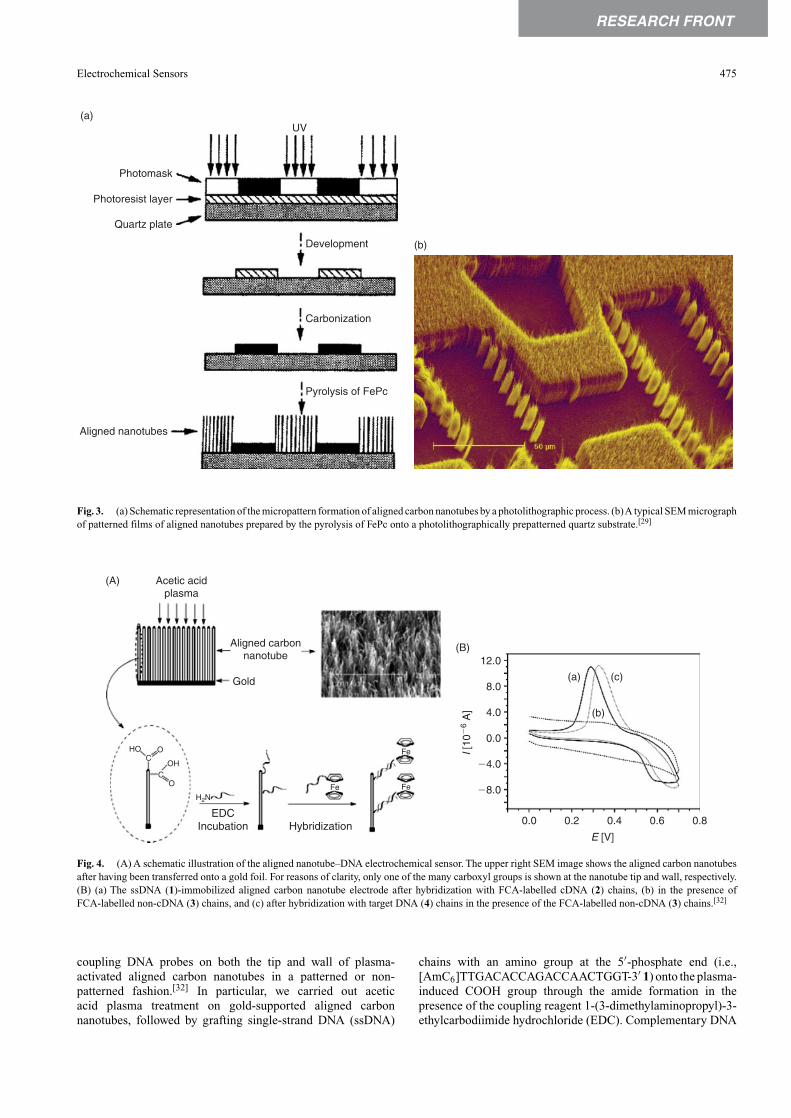
While working in CSIRO Molecular Science (now CSIROMolecular and Health Technologies) in Melbourne, we have pre-pared aligned carbon nanotubes by pyrolyzing iron(ii) phthalo-cyanine (FePc) under an Ar/H2 atmosphere at 800–1100◦C.[28]
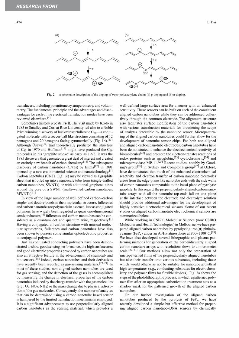
We have also developed several lithographic and plasma pat-terning methods for generation of the perpendicularly alignedcarbon nanotube arrays with resolutions down to a micrometerscale.[29–31] Our methods allow not only the preparation ofmicropatterned films of the perpendicularly aligned nanotubesbut also their transfer onto various substrates, including thosewhich would otherwise not be suitable for nanotube growth athigh temperatures (e.g., conducting substrates for electrochem-istry and polymer films for flexible devices). Fig. 3a shows thesteps of the photolithographic process, in which a patterned poly-mer film after an appropriate carbonization treatment acts as ashadow mask for the patterned growth of the aligned carbonnanotubes.
On our further investigation of the aligned carbonnanotubes produced by the pyrolysis of FePc, we haverecently developed a simple but effective method for prepar-ing aligned carbon nanotube–DNA sensors by chemically
RESEARCH FRONT
Electrochemical Sensors 475
Photomask
Photoresist layer
Quartz plate
Aligned nanotubes
UV
Development
Carbonization
Pyrolysis of FePc
(a)
(b)
Fig. 3. (a) Schematic representation of the micropattern formation of aligned carbon nanotubes by a photolithographic process. (b)A typical SEM micrographof patterned films of aligned nanotubes prepared by the pyrolysis of FePc onto a photolithographically prepatterned quartz substrate.[29]
Aligned carbon nanotube
EDCIncubation Hybridization
Gold
Acetic acidplasma
HO OC
COH
O
H2NFe
Fe
Fe
(A)
12.0
8.0
4.0
0.0
0.0 0.2 0.4 0.6 0.8
�4.0
�8.0
E [V]
I [10
�6
A]
(a) (c)
(b)
(B)
Fig. 4. (A) A schematic illustration of the aligned nanotube–DNA electrochemical sensor. The upper right SEM image shows the aligned carbon nanotubesafter having been transferred onto a gold foil. For reasons of clarity, only one of the many carboxyl groups is shown at the nanotube tip and wall, respectively.(B) (a) The ssDNA (1)-immobilized aligned carbon nanotube electrode after hybridization with FCA-labelled cDNA (2) chains, (b) in the presence ofFCA-labelled non-cDNA (3) chains, and (c) after hybridization with target DNA (4) chains in the presence of the FCA-labelled non-cDNA (3) chains.[32]
coupling DNA probes on both the tip and wall of plasma-activated aligned carbon nanotubes in a patterned or non-patterned fashion.[32] In particular, we carried out aceticacid plasma treatment on gold-supported aligned carbonnanotubes, followed by grafting single-strand DNA (ssDNA)
chains with an amino group at the 5′-phosphate end (i.e.,[AmC6]TTGACACCAGACCAACTGGT-3′ 1) onto the plasma-induced COOH group through the amide formation in thepresence of the coupling reagent 1-(3-dimethylaminopropyl)-3-ethylcarbodiimide hydrochloride (EDC). Complementary DNA
RESEARCH FRONT
476 L. Dai
(v)
(iv)
(i) (ii)
(iii)
TCA
(B: A, T, C, G)
T T18CACCGTTAAGCGCAT
NH4OH, 55°C
T T T
T
hν
�
N�
N
N
HO O HO
H3CO
IprN�POCH2CH2CN
OCH3
N
OO O
O
B
H3CO
OCH3
O O
O
OO
OO
N
O
OB
HO
N
O�POCH2CH2CN
O�POCH2CH2CN
B
N
(a)
100 nm
(b)
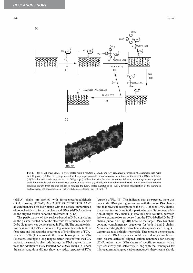
Fig. 5. (a) (i) Aligned MWNTs were coated with a solution of AZT, and UV-irradiated to produce photoadducts each withan OH group. (ii) The OH group reacted with a phosphoramidite mononucleotide to initiate synthesis of the DNA molecule.(iii) Trichloroacetic acid deprotected the OH group. (iv) Reaction with the next nucleotide followed, and the cycle was repeateduntil the molecule with the desired base sequence was made. (v) Finally, the nanotubes were heated in NH3 solution to removeblocking groups from the nucleotides to produce the DNA-coated nanotubes. (b) DNA-directed modification of the nanotubesurface with gold nanoparticles of different diameters (scale bar: 100 nm).[33]
(cDNA) chains pre-labelled with ferrocenecarboxaldehyde(FCA, forming [FCA-C6]ACCAGTTGGTCTGGTGTCAA-3′2) were then used for hybridizing with the surface-immobilizedoligonucleotides to form double-strand DNA (dsDNA) heliceson the aligned carbon nanotube electrodes (Fig. 4A).
The performance of the surface-bound ssDNA (1) chainson the plasma-treated nanotube electrode for sequence-specificDNA diagnoses was demonstrated in Fig. 4B. The strong oxida-tion peak seen at 0.29V in curve a of Fig. 4B can be attributable toferrocene and indicates the occurrence of hybridization of FCA-labelled cDNA (2) chains with the nanotube-supported ssDNA(1) chains, leading to a long-range electron transfer from the FCAprobe to the nanotube electrode through the DNA duplex. In con-trast, the addition of FCA-labelled non-cDNA chains (3) underthe same conditions did not show any redox response of FCA
(curve b of Fig. 4B). This indicates that, as expected, there wasno specific DNA pairing interaction with the non-cDNA chains,and that physical adsorption of the FCA-labelled DNA chains,if any, was insignificant in this particular case. Subsequent addi-tion of target DNA chains (4) into the above solution, however,led to a strong redox response from the FCA-labelled DNA (3)chains (curve c of Fig. 4B) because the target DNA (4) chaincontains complementary sequences for both 1 and 3 chains.More interestingly, the electrochemical responses seen in Fig. 4Bwere revealed to be highly reversible.These results demonstratedthat specific DNA sequences could be covalently immobilizedonto plasma-activated aligned carbon nanotubes for sensingcDNA and/or target DNA chains of specific sequences with ahigh sensitivity and selectivity. Along with the techniques formicropatterning aligned carbon nanotubes, these results should
RESEARCH FRONT
Electrochemical Sensors 477
Note:
SWCNT or MWCNT
ss DNA chain
c DNA chain
Gold particle
DNAhybridization
NH
NH
NH
NH
NH
NH
HN
HN
HN
HN
CO
C C
C
C
C
C
CCCO O
O O
O
O
O
O
O
�
(a)
0 2.50 5.000
2.50
5.00
µm
(b) (c)
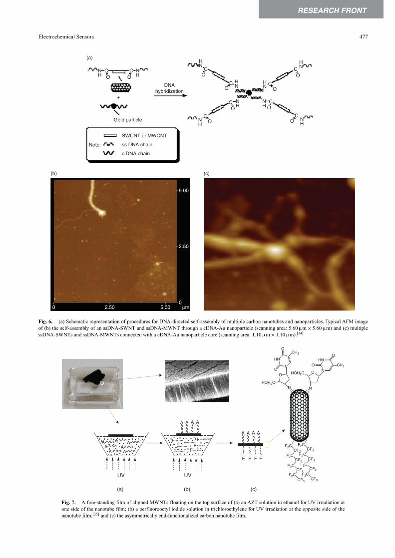
Fig. 6. (a) Schematic representation of procedures for DNA-directed self-assembly of multiple carbon nanotubes and nanoparticles. Typical AFM imageof (b) the self-assembly of an ssDNA-SWNT and ssDNA-MWNT through a cDNA-Au nanoparticle (scanning area: 5.60 µm × 5.60 µm) and (c) multiplessDNA-SWNTs and ssDNA-MWNTs connected with a cDNA-Au nanoparticle core (scanning area: 1.10 µm × 1.10 µm).[34]
UV
A A A A
UV
A A A A
AA
A
A
AA
F
F FF
F FFF
F F F
A
(a) (b) (c)
O
OO
O
O
O
HN HN
N
N
N
CH3
CH3
HOH2C
HOH2C
F2C
F2C
F2C
F2C F2C
F2C
F2C
F2CCF2
CF2
CF2
CF3CF3
CF2
CF2
CF2
N
Fig. 7. A free-standing film of aligned MWNTs floating on the top surface of (a) an AZT solution in ethanol for UV irradiation atone side of the nanotube film; (b) a perfluorooctyl iodide solution in trichloroethylene for UV irradiation at the opposite side of thenanotube film;[35] and (c) the asymmetrically end-functionalized carbon nanotube film.
RESEARCH FRONT
478 L. Dai
have important implications not only for the sequence-specificanalyses or diagnoses of DNA chains but also for the use ofcarbon nanotubes in advanced sensing chips.
Sensor chips (or sensor arrays) consist of many different sen-sors on a single chip, allowing the identification of complexmixture systems even without separation. The construction ofsensor chips requires multidimensional integration of functionalcomponents. Self-assembly could facilitate the development ofsensor chips by adding multifunctional supramolecular struc-tures to the existing sensing devices and systems. In collabo-ration with McCall and Moghaddam at CSIRO in Australia, wehave developed a photochemical method to functionalize carbonnanotubes with photoreactive reagents (e.g., aziridothymidine,AZT), followed by the coupling of ssDNA chains onto the car-bon nanotube through the photo-adduct and coating the nanotubesidewalls with cDNA-modified gold nanoparticles by means ofDNA hybridization (Fig. 5).[33]
The locations of the DNA molecules thus attached onto thecarbon nanotubes can be determined by a visual assay usingcDNA-modified gold nanoparticles and transmission electronmicroscopy (TEM). Fig. 5b shows gold nanoparticles positionedin close proximity to the surfaces of the nanotubes; the samplewas prepared by binding cDNA-attached 16-nm diameter goldnanoparticles to the ssDNA chains grafted on the nanotubes,followed by a further hybridizing of the remaining unboundcDNA on the 16-nm gold nanoparticles to their cDNA chainsattached to 38-nm diameter gold nanoparticles.
Therefore, the highly specific DNA hybridization reactioncan be used not only to develop the visual assay to check the exactlocations of DNA molecules attached to the nanotubes, but alsoto provide a means of self-assembling functional componentson the nanotube surface for potential applications, includingin sensor chips. Furthermore, we have also prepared a widerange of multicomponent structures of carbon nanotubes (Fig. 6)through DNA-direct self-assembly of carbon nanotubes and goldnanoparticles in solution for multifunctional material and deviceapplications.[34]
In somewhat related work, our[35] and Hinds’ group[36] inde-pendently reported asymmetric end-functionalization of carbonnanotubes. In particular, we developed a simple but effectivephotochemical approach to directly grafting different chemi-cal reagents onto the opposite tube-ends of individual carbonnanotubes, as schematically shown in Fig. 7. The resultant nano-tubes with different chemical reagents (e.g., ssDNA and cDNAchains) attached onto their opposite tube-ends should be veryuseful for site-selective self-assembly of carbon nanotubes intomany novel functional structures even without the involvementof nanoparticles.
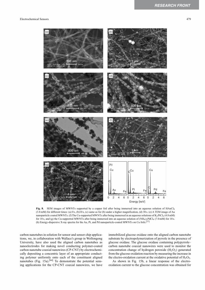
More recently, we have developed a facile yet versatileand effective substrate-enhanced electroless deposition (SEED)method for decorating CNTs with various metal nanoparticles,including those otherwise impossible by more conventional elec-troless deposition methods, in the absence of any additionalreducing agent.[37,38] By simply supporting carbon nanotubeswith a metal substrate of a redox potential lower than thatof the metal ions to be reduced into nanoparticles, we haverecently used the SEED method to deposit metal (Cu, Ag, Au,Pt, and Pd) nanoparticles onto SWNTs and MWNTs (Fig. 8).[37]
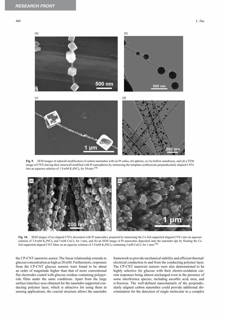
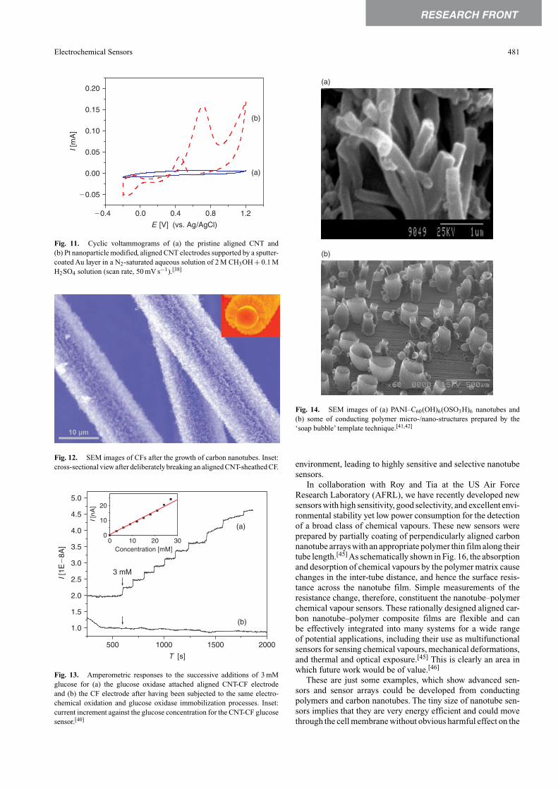
In conjunction with shape- and size-controlled metal nanopar-ticle syntheses, the SEED technique described above furtherenabled us to successfully deposit the shape/size-controlledmetal nanoparticles either on the nanotube outer or inner wall(Fig. 9).[38] Our preliminary results have also demonstrated that
the SEED method can be used to graft metal nanoparticles ontothe aligned/micropatterned carbon nanotubes, either along thenanotube length or on nanotube tips, while largely retaining theirstructural integrity (Fig. 10).
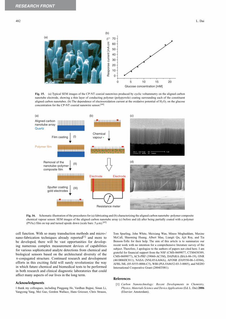
To study the electrochemical activity of the CNTs modifiedwith metal nanoparticles, we used the FePc-generated alignedCNTs modified with Pt nanocubes as the working electrodefor electrocatalytic oxidation of methanol. As can be seen inFig. 11, the pristine, aligned CNT electrode showed a capaci-tive current only due to the double layer capacitance (Fig. 11a),whereas the Pt nanoparticle modified, aligned CNT electrodeshowed two strong redox peaks at 0.45 and 0.7V, characteristic ofmethanol oxidation.[38] These results indicate the usefulness ofthe metal nanoparticle modified, aligned CNT arrays as efficientelectrodes in methanol direct fuel cells and perhaps many otherelectrochemical systems, including sensors and sensor chips.
Furthermore, we have successfully prepared multicomponentand multifunctional hybrid structures based on microsized car-bon fibres (CFs) sheathed with aligned carbon nanotubes andtheir derivatives (Fig. 12),[39] which were demonstrated to bean effective means for connecting nanoscale entities to the out-side world and to possess interesting electrochemical propertiesattractive for a wide range of potential applications, includingin methanol direct fuel cells, highly sensitive chemical- andbio-sensors.[39]
Fig. 13 shows amperometric responses for a glucose oxidaseimmobilized aligned CNTs on the CF substrate (curve a) andthe pristine CF electrode (curve b) to each successive additionof 3 mM glucose. As can be seen, a stepwise increase in the cur-rent signal upon each successive addition of glucose (curve a)was observed, while the CF electrode showed no obvious currentchange with the addition of glucose (curve b). Also included inthe inset of Fig. 13 is the current increment with the glucoseconcentration for the CNT-CF electrode, which shows a pseudo-linear relationship indicating a high sensitivity and reliability.The linear response to the glucose concentration extends beyond20 mM, which is higher than the 15 mM required for practicaluse in the detection of blood glucose.[40] The CNT-CF glucosesensor also shows a fast response, reaching to a steady-state cur-rent signal within about 20 s upon each addition of the glucoseto the detecting solution. Given that many enzymatic reactionsare associated with the generation of hydrogen peroxide, themethodology developed in this study should be applicable tosensor many other biologically important substances. Judiciousmodification of the CF-supported aligned carbon nanotubes withvarious functional moieties could lead to a class of novel multi-dimensional, multicomponent, and multifunctional materials ofpractical significance.
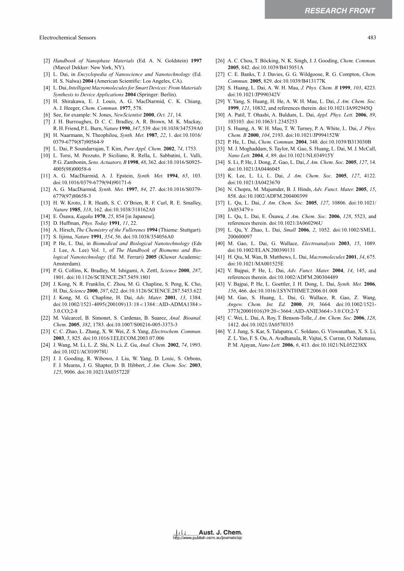
On the other hand, we have recently synthesized, incollaboration with Wan’s group at the Chinese Academy ofSciences, polyaniline (PANI) nanotubes (Fig. 14a) through aself-assembled C60(OH)6(OSO3H)6 supramolecular templateusing (NH4)2S2O8 as an oxidant.[41] This, together with themore recent discovery of patterned and non-patterned generationof conducting polymer micro-/nano-containers self-assembledaround the surface of ‘soap bubbles’ produced on an electrodeby electrolysis of appropriate electrolyte solutions (Fig. 14b),[42]
clearly indicates that supramolecular engineering has broadenedthe scope for developing multidimensional and multifunctionalπ-conjugated structures of significance for sensor and sensorchip applications.[43]
In addition to the chemical grafting of DNA chains ontothe carbon nanotube surface and DNA-directed self-assembling
RESEARCH FRONT
Electrochemical Sensors 479
0 2 4 6 0 2 4 6 0 2 4 6
Energy [keV]
(a) (b)
(c) (d)
(e) (f)
(g) (h)
Cu
Au Fe
C
C
C
Cu
PdFe
Cu
Pt Fe
Fig. 8. SEM images of MWNTs supported by a copper foil after being immersed into an aqueous solution of HAuCl4(3.8 mM) for different times: (a) 0 s, (b)10 s, (c) same as for (b) under a higher magnification, (d) 30 s. (e) A TEM image of Aunanoparticle coated MWNTs. (f) The Cu-supported MWNTs after being immersed in an aqueous solutions of K2PtCl4 (4.8 mM)for 10 s, and (g) the Cu-supported MWNTs after being immersed into an aqueous solution of (NH4)2PdCl4 (7.0 mM) for 10 s.(h) Energy-dispersive X-ray spectra for the Au, Pt, and Pd nanoparticle-coated MWNTs on Cu foils.[37]
carbon nanotubes in solution for sensor and sensor chip applica-tions, we, in collaboration with Wallace’s group in WollongongUniversity, have also used the aligned carbon nanotubes asnanoelectrodes for making novel conducting polymer-coatedcarbon nanotube coaxial nanowires (CP-CNT) by electrochemi-cally depositing a concentric layer of an appropriate conduct-ing polymer uniformly onto each of the constituent alignednanotubes (Fig. 15a).[44] To demonstrate the potential sens-ing applications for the CP-CNT coaxial nanowires, we have
immobilized glucose oxidase onto the aligned carbon nanotubesubstrate by electropolymerization of pyrrole in the presence ofglucose oxidase. The glucose oxidase containing polypyrrole–carbon nanotube coaxial nanowires were used to monitor theconcentration change of hydrogen peroxide (H2O2) generatedfrom the glucose oxidation reaction by measuring the increase inthe electro-oxidation current at the oxidative potential of H2O2.
As shown in Fig. 15b, a linear response of the electro-oxidation current to the glucose concentration was obtained for
RESEARCH FRONT
480 L. Dai
(a) (b)
(c) (d)
Fig. 9. SEM images of sidewall modification of carbon nanotubes with (a) Pt cubes, (b) spheres, (c) Au hollow nanoboxes, and (d) a TEMimage of CNTs having their innerwall modified with Pt nanospheres by immersing the template-synthesized, perpendicularly aligned CNTsinto an aqueous solution of 1.9 mM K2PtCl4 for 30 min.[38]
(a) (b)
Fig. 10. SEM images of (a) aligned CNTs decorated with Pt nanocubes, prepared by immersing the Cu foil-supported aligned CNTs into an aqueoussolution of 3.8 mM K2PtCl4 and 5 mM CuCl2 for 1 min, and (b) an SEM image of Pt nanocubes deposited onto the nanotube tips by floating the Cufoil-supported aligned CNT films on an aqueous solution of 3.8 mM K2PtCl4 containing 5 mM CuCl2 for 1 min.[38]
the CP-CNT nanowire sensor. The linear relationship extends toglucose concentration as high as 20 mM. Furthermore, responsesfrom the CP-CNT glucose sensors were found to be aboutan order of magnitude higher than that of more conventionalflat electrodes coated with glucose oxidase containing polypyr-role films under the same conditions. Apart from the largesurface/interface area obtained for the nanotube-supported con-ducting polymer layer, which is attractive for using them insensing applications, the coaxial structure allows the nanotube
framework to provide mechanical stability and efficient thermal/electrical conduction to and from the conducting polymer layer.The CP-CNT nanowire sensors were also demonstrated to behighly selective for glucose with their electro-oxidation cur-rent responses being almost unchanged even in the presence ofsome interference species, including ascorbic acid, urea, andd-fructose. The well-defined nanochannels of the perpendic-ularly aligned carbon nanotubes could provide additional dis-crimination for the detection of single molecular in a complex
RESEARCH FRONT
Electrochemical Sensors 481
�0.4 0.0 0.4 0.8 1.2
�0.05
0.00
0.05
0.10
0.15
0.20
(b)
(a)
I [m
A]
E [V] (vs. Ag/AgCl)
Fig. 11. Cyclic voltammograms of (a) the pristine aligned CNT and(b) Pt nanoparticle modified, aligned CNT electrodes supported by a sputter-coated Au layer in a N2-saturated aqueous solution of 2 M CH3OH + 0.1 MH2SO4 solution (scan rate, 50 mV s−1).[38]
Fig. 12. SEM images of CFs after the growth of carbon nanotubes. Inset:cross-sectional view after deliberately breaking an aligned CNT-sheathed CF.
500 1000 1500 2000
1.0
1.5
2.0
2.5
3.0
3.5
4.0
4.5
5.0
3 mM
(a)
(b)
I [nA
]
Concentration [mM]
I [1E
�8A
]
T [s]
0 10 20 300
10
20
Fig. 13. Amperometric responses to the successive additions of 3 mMglucose for (a) the glucose oxidase attached aligned CNT-CF electrodeand (b) the CF electrode after having been subjected to the same electro-chemical oxidation and glucose oxidase immobilization processes. Inset:current increment against the glucose concentration for the CNT-CF glucosesensor.[40]
(a)
(b)
Fig. 14. SEM images of (a) PANI–C60(OH)6(OSO3H)6 nanotubes and(b) some of conducting polymer micro-/nano-structures prepared by the‘soap bubble’ template technique.[41,42]
environment, leading to highly sensitive and selective nanotubesensors.
In collaboration with Roy and Tia at the US Air ForceResearch Laboratory (AFRL), we have recently developed newsensors with high sensitivity, good selectivity, and excellent envi-ronmental stability yet low power consumption for the detectionof a broad class of chemical vapours. These new sensors wereprepared by partially coating of perpendicularly aligned carbonnanotube arrays with an appropriate polymer thin film along theirtube length.[45] As schematically shown in Fig. 16, the absorptionand desorption of chemical vapours by the polymer matrix causechanges in the inter-tube distance, and hence the surface resis-tance across the nanotube film. Simple measurements of theresistance change, therefore, constituent the nanotube–polymerchemical vapour sensors. These rationally designed aligned car-bon nanotube–polymer composite films are flexible and canbe effectively integrated into many systems for a wide rangeof potential applications, including their use as multifunctionalsensors for sensing chemical vapours, mechanical deformations,and thermal and optical exposure.[45] This is clearly an area inwhich future work would be of value.[46]
These are just some examples, which show advanced sen-sors and sensor arrays could be developed from conductingpolymers and carbon nanotubes. The tiny size of nanotube sen-sors implies that they are very energy efficient and could movethrough the cell membrane without obvious harmful effect on the
RESEARCH FRONT
482 L. Dai
0
0
10
20
30
40
50
60
70
5 10 15 20
Glucose concentration [mM]
Res
pons
e cu
rren
t [m
Acm
�2 ](a)
(b)
Fig. 15. (a) Typical SEM images of the CP-NT coaxial nanowires produced by cyclic voltammetry on the aligned carbonnanotube electrode, showing a thin layer of conducting polymer (polypyrrole) coating surrounding each of the constituentaligned carbon nanotubes. (b) The dependence of electrooxidation current at the oxidative potential of H2O2 on the glucoseconcentration for the CP-NT coaxial nanowire sensor.[44]
(a) (b)
Chemicalvapour
Resistance meter
Electrode Electrode
Aligned carbonnanotube array
Film casting (I)
(II)
(III)
Removal of thenanotube–polymercomposite film
Sputter coatinggold electrodes
Quartz
Polymer film
(c)
(d)
Fig. 16. Schematic illustration of the procedures for (a) fabricating and (b) characterizing the aligned carbon nanotube–polymer compositechemical vapour sensor. SEM images of the aligned carbon nanotube array (c) before and (d) after being partially coated with a polymer(PVAc) film on top and turned upside down (scale bars: 5 µm).[45]
cell function. With so many transduction methods and micro-/nano-fabrication techniques already reported[1] and more tobe developed, there will be vast opportunities for develop-ing numerous complex measurement devices of capabilitiesfor various sophisticated analyte detections from chemical andbiological sensors based on the architectural diversity of theπ-conjugated structure. Continued research and developmentefforts in this exciting field will surely revolutionize the wayin which future chemical and biomedical tests to be performedin both research and clinical diagnostic laboratories that couldaffect many aspects of our lives in the long term.
AcknowledgmentsI thank my colleagues, including Pinggang He, Vardhan Bajpai, Sinan Li,Yangyong Yang, Mei Gao, Gordon Wallace, Hans Griesser, Chris Strauss,
Tom Spurling, John White, Meixiang Wan, Minoo Moghaddam, MaxineMcCall, Shaoming Huang, Albert Mau, Liangti Qu, Ajit Roy, and TiaBenson-Tolle for their help. The aim of this article is to summarize ourrecent work with no intention for a comprehensive literature survey of thesubject. Therefore, I apologize to the authors of papers not cited here. I amgrateful for financial support from the NSF (CMS-0609077, CTS0438389,CMS-0609077), ACS-PRF (39060-AC5M), DAPARA (BAA-06-19), ONR(461B06DC011), NASA (NNL05AA04A), AFOSR (FA9550-06-1-0384),AFRL/ML (05-S555-0006-C5), WBI (PIA FA8652-03-3-0005), and NEDOInternational Cooperative Grant (2004IT081).
References[1] Carbon Nanotechnology: Recent Developments in Chemistry,
Physics, Materials Science and DeviceApplications (Ed. L. Dai) 2006(Elsevier: Amsterdam).
RESEARCH FRONT
Electrochemical Sensors 483
[2] Handbook of Nanophase Materials (Ed. A. N. Goldstein) 1997(Marcel Dekker: New York, NY).
[3] L. Dai, in Encyclopedia of Nanoscience and Nanotechnology (Ed.H. S. Nalwa) 2004 (American Scientific: Los Angeles, CA).
[4] L. Dai, Intelligent Macromolecules for Smart Devices: From MaterialsSynthesis to Device Applications 2004 (Springer: Berlin).
[5] H. Shirakawa, E. J. Louis, A. G. MacDiarmid, C. K. Chiang,A. J. Heeger, Chem. Commun. 1977, 578.
[6] See, for example: N. Jones, NewScientist 2000, Oct. 21, 14.[7] J. H. Burroughes, D. C. C. Bradley, A. R. Brown, M. K. Mackay,
R. H. Friend, P. L. Burn, Nature 1990, 347, 539. doi:10.1038/347539A0[8] H. Naarmann, N. Theophilou, Synth. Met. 1987, 22, 1. doi:10.1016/
0379-6779(87)90564-9[9] L. Dai, P. Soundarrajan, T. Kim, Pure Appl. Chem. 2002, 74, 1753.
[10] L. Torsi, M. Pezzuto, P. Siciliano, R. Rella, L. Sabbatini, L. Valli,P. G. Zambonin, Sens.Actuators, B 1998, 48, 362. doi:10.1016/S0925-4005(98)00058-6
[11] A. G. MacDiarmid, A. J. Epstein, Synth. Met. 1994, 65, 103.doi:10.1016/0379-6779(94)90171-6
[12] A. G. MacDiarmid, Synth. Met. 1997, 84, 27. doi:10.1016/S0379-6779(97)80658-3
[13] H. W. Kroto, J. R. Heath, S. C. O’Brien, R. F. Curl, R. E. Smalley,Nature 1985, 318, 162. doi:10.1038/318162A0
[14] E. Osawa, Kagaku 1970, 25, 854 [in Japanese].[15] D. Huffman, Phys. Today 1991, 11, 22.[16] A. Hirsch, The Chemistry of the Fullerenes 1994 (Thieme: Stuttgart).[17] S. Iijima, Nature 1991, 354, 56. doi:10.1038/354056A0[18] P. He, L. Dai, in Biomedical and Biological Nanotechnology (Eds
J. Lee, A. Lee) Vol. 1, of The Handbook of Biomems and Bio-logical Nanotechnology (Ed. M. Ferrari) 2005 (Kluwer Academic:Amsterdam).
[19] P. G. Collins, K. Bradley, M. Ishigami, A. Zettl, Science 2000, 287,1801. doi:10.1126/SCIENCE.287.5459.1801
[20] J. Kong, N. R. Franklin, C. Zhou, M. G. Chapline, S. Peng, K. Cho,H. Dai, Science 2000, 287, 622. doi:10.1126/SCIENCE.287.5453.622
[21] J. Kong, M. G. Chapline, H. Dai, Adv. Mater. 2001, 13, 1384.doi:10.1002/1521-4095(200109)13:18<1384::AID-ADMA1384>
3.0.CO;2-8[22] M. Valcarcel, B. Simonet, S. Cardenas, B. Suarez, Anal. Bioanal.
Chem. 2005, 382, 1783. doi:10.1007/S00216-005-3373-3[23] C. C. Zhao, L. Zhang, X. W. Wei, Z. S. Yang, Electrochem. Commun.
2003, 5, 825. doi:10.1016/J.ELECOM.2003.07.006[24] J. Wang, M. Li, L. Z. Shi, N. Li, Z. Gu, Anal. Chem. 2002, 74, 1993.
doi:10.1021/AC010978U[25] J. J. Gooding, R. Wibowo, J. Liu, W. Yang, D. Losic, S. Orbons,
F. J. Mearns, J. G. Shapter, D. B. Hibbert, J. Am. Chem. Soc. 2003,125, 9006. doi:10.1021/JA035722F
[26] A. C. Chou, T. Böcking, N. K. Singh, J. J. Gooding, Chem. Commun.2005, 842. doi:10.1039/B415051A
[27] C. E. Banks, T. J. Davies, G. G. Wildgoose, R. G. Compton, Chem.Commun. 2005, 829. doi:10.1039/B413177K
[28] S. Huang, L. Dai, A. W. H. Mau, J. Phys. Chem. B 1999, 103, 4223.doi:10.1021/JP990342V
[29] Y. Yang, S. Huang, H. He, A. W. H. Mau, L. Dai, J. Am. Chem. Soc.1999, 121, 10832, and references therein. doi:10.1021/JA992945Q
[30] A. Patil, T. Ohashi, A. Buldum, L. Dai, Appl. Phys. Lett. 2006, 89,103103. doi:10.1063/1.2345253
[31] S. Huang, A. W. H. Mau, T. W. Turney, P. A. White, L. Dai, J. Phys.Chem. B 2000, 104, 2193. doi:10.1021/JP994152W
[32] P. He, L. Dai, Chem. Commun. 2004, 348. doi:10.1039/B313030B[33] M. J. Moghaddam, S. Taylor, M. Gao, S. Huang, L. Dai, M. J. McCall,
Nano Lett. 2004, 4, 89. doi:10.1021/NL034915Y[34] S. Li, P. He, J. Dong, Z. Gao, L. Dai, J. Am. Chem. Soc. 2005, 127, 14.
doi:10.1021/JA0446045[35] K. Lee, L. Li, L. Dai, J. Am. Chem. Soc. 2005, 127, 4122.
doi:10.1021/JA0423670[36] N. Chopra, M. Majumder, B. J. Hinds, Adv. Funct. Mater. 2005, 15,
858. doi:10.1002/ADFM.200400399[37] L. Qu, L. Dai, J. Am. Chem. Soc. 2005, 127, 10806. doi:10.1021/
JA053479+[38] L. Qu, L. Dai, E. Osawa, J. Am. Chem. Soc. 2006, 128, 5523, and
references therein. doi:10.1021/JA060296U[39] L. Qu, Y. Zhao, L. Dai, Small 2006, 2, 1052. doi:10.1002/SMLL.
200600097[40] M. Gao, L. Dai, G. Wallace, Electroanalysis 2003, 15, 1089.
doi:10.1002/ELAN.200390131[41] H. Qiu, M. Wan, B. Matthews, L. Dai, Macromolecules 2001, 34, 675.
doi:10.1021/MA001525E[42] V. Bajpai, P. He, L. Dai, Adv. Funct. Mater. 2004, 14, 145, and
references therein. doi:10.1002/ADFM.200304489[43] V. Bajpai, P. He, L. Goettler, J. H. Dong, L. Dai, Synth. Met. 2006,
156, 466. doi:10.1016/J.SYNTHMET.2006.01.008[44] M. Gao, S. Huang, L. Dai, G. Wallace, R. Gao, Z. Wang,
Angew. Chem. Int. Ed. 2000, 39, 3664. doi:10.1002/1521-3773(20001016)39:20<3664::AID-ANIE3664>3.0.CO;2-Y
[45] C. Wei, L. Dai, A. Roy, T. Benson-Tolle, J. Am. Chem. Soc. 2006, 128,1412. doi:10.1021/JA0570335
[46] Y. J. Jung, S. Kar, S. Talapatra, C. Soldano, G. Viswanathan, X. S. Li,Z. L.Yao, F. S. Ou, A. Avadhanula, R. Vajtai, S. Curran, O. Nalamasu,P. M. Ajayan, Nano Lett. 2006, 6, 413. doi:10.1021/NL052238X
Top Related