


γλώσσες
Σελίδες
Νομικός

Rev. 1.17/2011
Page 1 of 18
V•I CHIP CORP. (A VICOR COMPANY) 25 FRONTAGE RD. ANDOVER, MA 01810 800-735-6200
vicorpower.com
x 040 200A00yB48BCM
PRELIMINARY DATASHEET
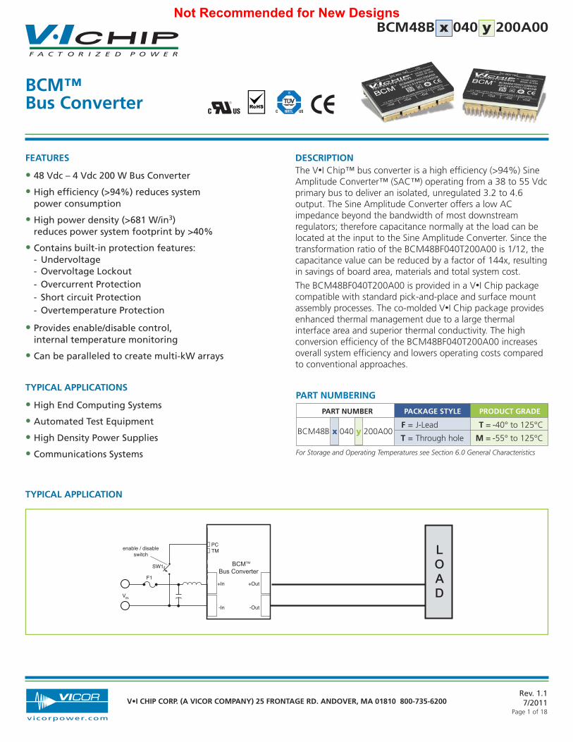
BCM™ Bus Converter
SW1
enable / disableswitch
F1
VIN
PCTM
-Out
+Out
-In
+In
LOAD
BCMTM Bus Converter
FEATURES
• 48 Vdc – 4 Vdc 200 W Bus Converter
• High efficiency (>94%) reduces systempower consumption
• High power density (>681 W/in3) reduces power system footprint by >40%
• Contains built-in protection features:- Undervoltage- Overvoltage Lockout- Overcurrent Protection- Short circuit Protection- Overtemperature Protection
• Provides enable/disable control, internal temperature monitoring
• Can be paralleled to create multi-kW arrays
TYPICAL APPLICATIONS
• High End Computing Systems
• Automated Test Equipment
• High Density Power Supplies
• Communications Systems
DESCRIPTIONThe V•I Chip™ bus converter is a high efficiency (>94%) SineAmplitude Converter™ (SAC™) operating from a 38 to 55 Vdcprimary bus to deliver an isolated, unregulated 3.2 to 4.6output. The Sine Amplitude Converter offers a low ACimpedance beyond the bandwidth of most downstreamregulators; therefore capacitance normally at the load can belocated at the input to the Sine Amplitude Converter. Since thetransformation ratio of the BCM48BF040T200A00 is 1/12, thecapacitance value can be reduced by a factor of 144x, resultingin savings of board area, materials and total system cost.
The BCM48BF040T200A00 is provided in a V•I Chip packagecompatible with standard pick-and-place and surface mountassembly processes. The co-molded V•I Chip package providesenhanced thermal management due to a large thermalinterface area and superior thermal conductivity. The highconversion efficiency of the BCM48BF040T200A00 increasesoverall system efficiency and lowers operating costs comparedto conventional approaches.
TYPICAL APPLICATION
C US®
S
NRTLC US
PART NUMBER PACKAGE STYLE PRODUCT GRADE
F = J-Lead T = -40° to 125°C
T = Through hole M = -55° to 125°C
PART NUMBERING
For Storage and Operating Temperatures see Section 6.0 General Characteristics
040x y 200A00B48BCM
Not Recommended for New Designs
Rev. 1.17/2011
Page 2 of 18
V•I CHIP CORP. (A VICOR COMPANY) 25 FRONTAGE RD. ANDOVER, MA 01810 800-735-6200
vicorpower.com
x 040 200A00yB48BCMPRELIMINARY DATASHEET
ATTRIBUTE SYMBOL CONDITIONS / NOTES MIN TYP MAX UNIT
POWERTRAIN
Input voltage range, continuous VIN_DC 38 55 V
Input voltage range, transient VIN_TRANSFull current or power supported, 50 ms max, 38 55 V10% duty cycle max
Quiescent current IQ Disabled, PC Low 0.5 1.0 mA
VIN to VOUT time TON1 VIN = 48 V, PC floating 450 650 800 ms
No load power dissipation PNL
VIN = 48 V, TC = 25ºC 4.9 6.3
WVIN = 48 V 1.5 10.0
VIN = 38 V to 55 V, TC = 25ºC 8
VIN = 38 V to 55 V 12
Inrush current peak IINR_PWorse case of: VIN = 55 V, COUT = 9100 µF,
10 20 ARLOAD = 73 mΩDC input current IIN_DC At POUT= 200 W 5 A
Transformation ratio K K = VOUT/ VIN, at no load 1/12 V/V
Output power (average) POUT_AVG 200 W
Output power (peak) POUT_PK 10 ms max, POUT_AVG ≤ 200 W 300 W
Output current (average) IOUT_AVG 53 A
Output current (peak) IOUT_PK 10 ms max, IOUT_AVG ≤ 53 A 75 A
VIN = 48 V, IOUT = 50 A; Tc = 25°C 93.5 94.5
Efficiency (ambient) ηAMB VIN = 38 V to 55 V, IOUT = 50 A; Tc = 25°C 90.5 %
VIN = 48 V, IOUT = 25 A; Tc = 25°C 92.5 93.6
Efficiency (hot) ηHOT VIN = 48 V, IOUT = 50 A; Tc = 100°C 93.4 94.4 %
Efficiency (over load range) η20% 10 A < IOUT < 50 A 80.5 %
ROUT_COLD IOUT = 50 A, Tc = -40°C 1.5 1.75 2.2 mΩOutput resistance ROUT_AMB IOUT = 50 A, Tc = 25°C 1.8 2.2 2.7 mΩ
ROUT_HOT IOUT = 50 A, TC = 100°C 2.3 2.6 3.1 mΩSwitching frequency FSW 1.36 1.43 1.50 MHz
Output voltage ripple VOUT_PPCOUT = 0 F, IOUT = 50 A, VIN = 48 V,
216 350 mV20 MHz BW, Section 10
Output inductance (parasitic) LOUT_PARFrequency up to 30 MHz,
600 pHSimulated J-lead model
Output capacitance (internal) COUT_INT Effective value at 4 VOUT 200 µF
Output capacitance (external) COUT_EXT 0 9100 µF
1.0 ABSOLUTE MAXIMUM VOLTAGE RATINGS
The absolute maximum ratings below are stress ratings only. Operation at or beyond these maximum ratings can cause permanentdamage to the device.
2.0 ELECTRICAL CHARACTERISTICS
Specifications apply over all line and load conditions unless otherwise noted; Boldface specifications apply over the temperaturerange of -40°C < TC < 100°C (T-Grade); All other specifications are at TC = 25ºC unless otherwise noted.
MIN MAX UNIT
+IN to –IN . . . . . . . . . . . . . . . . . . . . . . . -1 60 V
VIN slew rate (operational) . . . . . . . . . -1 1 V/µsIsolation voltage, input to output . . . . 2250 V
+OUT to –OUT . . . . . . . . . . . . . . . . . . . -1 10 V
Output current transient(< = 10 ms, < = 10% DC) . . . . . . . . . . . . -3 75 A
MIN MAX UNIT
Output current average . . . . . . . . . . . . -2 53 A
PC to –IN . . . . . . . . . . . . . . . . . . . . . . . . -0.3 20 V
TM to –IN . . . . . . . . . . . . . . . . . . . . . . . -0.3 7 V
Operating IC junction temperature . . -40 125 °C
Storage temperature . . . . . . . . . . . . . . -40 125 °C
Not Recommended for New Designs
Rev. 1.17/2011
Page 3 of 18
V•I CHIP CORP. (A VICOR COMPANY) 25 FRONTAGE RD. ANDOVER, MA 01810 800-735-6200
vicorpower.com
x 040 200A00yB48BCMPRELIMINARY DATASHEET
2.0 ELECTRICAL CHARACTERISTICS (CONT.)
ATTRIBUTE SYMBOL CONDITIONS / NOTES MIN TYP MAX UNIT
PROTECTION
Input overvoltage lockout threshold VIN_OVLO+ 55.1 58.5 60 V
Input overvoltage recovery threshold VIN_OVLO- 55.1 58.0 60 V
Input overvoltage lockout hysteresis VIN_OVLO_HYST 1.2 V
Overvoltage lockout response time TOVLO 8 µs
Fault recovery time TAUTO_RESTART 320 420 530 ms
Input undervoltage lockout threshold VIN_UVLO- 28.5 31.1 37.4 V
Input undervoltage recovery threshold VIN_UVLO+ 28.5 33.7 37.4 V
Input undervoltage lockout hysteresis VIN_UVLO_HYST 1.6 V
Undervoltage lockout response time TUVLO 8 µs
Output overcurrent trip threshold IOCP 53 78 100 A
Output overcurrent response time constant TOCP Effective internal RC filter 6.2 ms
Short circuit protection trip threshold ISCP 100 A
Short circuit protection response time TSCP 1 µs
Thermal shutdown threshold TJ_OTP 125 ºC
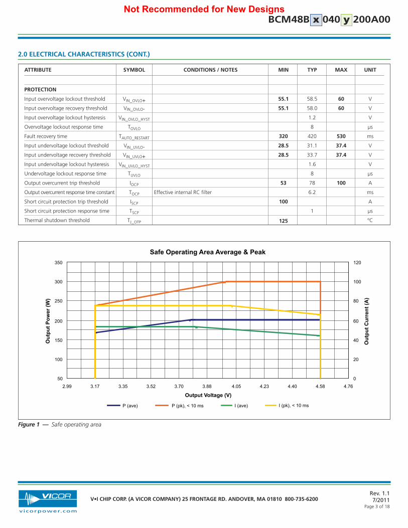
Safe Operating Area Average & Peak
Output Voltage (V)
Ou
tpu
t P
ow
er
(W)
P (ave) P (pk), < 10 ms I (ave) I (pk), < 10 ms
Ou
tpu
t C
urr
en
t (A
)
50
100
150
200
250
300
350
2.99 3.17 3.35 3.52 3.70 3.88 4.05 4.23 4.40 4.58 4.76
0
20
40
60
80
100
120
Figure 1 — Safe operating area
Not Recommended for New Designs
Rev. 1.17/2011
Page 4 of 18
V•I CHIP CORP. (A VICOR COMPANY) 25 FRONTAGE RD. ANDOVER, MA 01810 800-735-6200
vicorpower.com
x 040 200A00yB48BCMPRELIMINARY DATASHEET
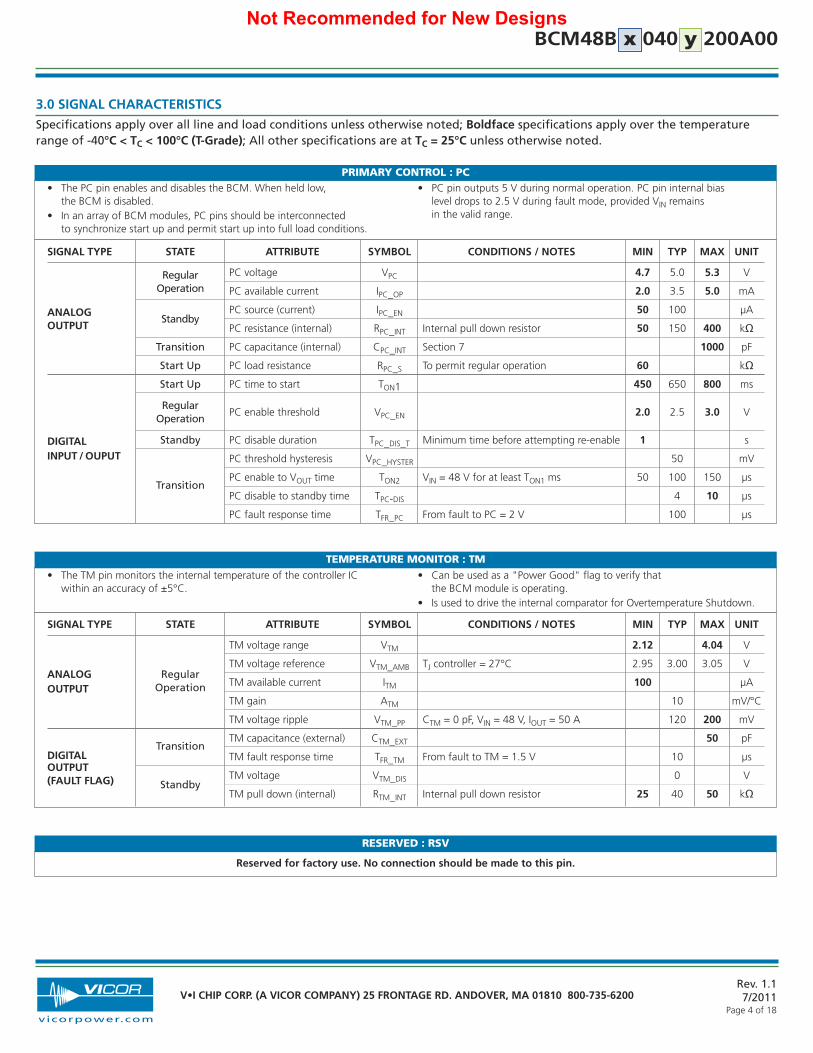
3.0 SIGNAL CHARACTERISTICS
Specifications apply over all line and load conditions unless otherwise noted; Boldface specifications apply over the temperaturerange of -40°C < TC < 100°C (T-Grade); All other specifications are at TC = 25°C unless otherwise noted.
SIGNAL TYPE STATE ATTRIBUTE SYMBOL CONDITIONS / NOTES MIN TYP MAX UNIT
Regular PC voltage VPC 4.7 5.0 5.3 V
Operation PC available current IPC_OP 2.0 3.5 5.0 mA
ANALOGStandby
PC source (current) IPC_EN 50 100 µA
OUTPUT PC resistance (internal) RPC_INT Internal pull down resistor 50 150 400 kΩTransition PC capacitance (internal) CPC_INT Section 7 1000 pF
Start Up PC load resistance RPC_S To permit regular operation 60 kΩStart Up PC time to start TON1 450 650 800 ms
RegularPC enable threshold VPC_EN 2.0 2.5 3.0 V
Operation
DIGITAL Standby PC disable duration TPC_DIS_T Minimum time before attempting re-enable 1 s
INPUT / OUPUT PC threshold hysteresis VPC_HYSTER 50 mV
TransitionPC enable to VOUT time TON2 VIN = 48 V for at least TON1 ms 50 100 150 µs
PC disable to standby time TPC-DIS 4 10 µs
PC fault response time TFR_PC From fault to PC = 2 V 100 µs
• The PC pin enables and disables the BCM. When held low, the BCM is disabled.
• In an array of BCM modules, PC pins should be interconnected to synchronize start up and permit start up into full load conditions.
• PC pin outputs 5 V during normal operation. PC pin internal bias level drops to 2.5 V during fault mode, provided VIN remains in the valid range.
PRIMARY CONTROL : PC
SIGNAL TYPE STATE ATTRIBUTE SYMBOL CONDITIONS / NOTES MIN TYP MAX UNIT
TM voltage range VTM 2.12 4.04 V
RegularTM voltage reference VTM_AMB TJ controller = 27°C 2.95 3.00 3.05 V
ANALOGOperation TM available current ITM 100 µA
OUTPUTTM gain ATM 10 mV/°C
TM voltage ripple VTM_PP CTM = 0 pF, VIN = 48 V, IOUT = 50 A 120 200 mV
DIGITALTransition
TM capacitance (external) CTM_EXT 50 pF
OUTPUT TM fault response time TFR_TM From fault to TM = 1.5 V 10 µs
(FAULT FLAG) StandbyTM voltage VTM_DIS 0 V
TM pull down (internal) RTM_INT Internal pull down resistor 25 40 50 kΩ
• The TM pin monitors the internal temperature of the controller IC within an accuracy of ±5°C.
• Can be used as a "Power Good" flag to verify that the BCM module is operating.
• Is used to drive the internal comparator for Overtemperature Shutdown.
TEMPERATURE MONITOR : TM
Reserved for factory use. No connection should be made to this pin.
RESERVED : RSV
Not Recommended for New Designs
Rev. 1.17/2011
Page 5 of 18
V•I CHIP CORP. (A VICOR COMPANY) 25 FRONTAGE RD. ANDOVER, MA 01810 800-735-6200
vicorpower.com
x 040 200A00yB48BCMPRELIMINARY DATASHEET
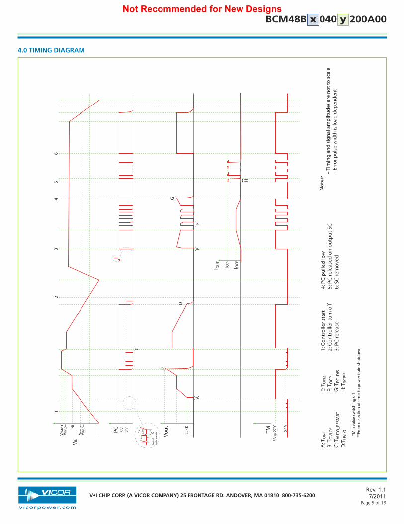
4.0 TIMING DIAGRAM1
23
45
6
V UVL
O+
PC 5 V
3 V
LL •
K
A: T
ON
1B:
TO
VLO
*C:
TAU
TO_R
ESTA
RTD
:TU
VLO
E: T
ON
2F:
TO
CPG
: TPC
–DIS
H: T
SCP*
*
1: C
ontr
olle
r sta
rt2:
Con
trol
ler t
urn
off3:
PC
rele
ase
4: P
C pu
lled
low
5: P
C re
leas
ed o
n ou
tput
SC
6: S
C re
mov
ed
Vout TM
3 V
@ 2
7°C
0.4
V
V IN 3
V5
V2.
5 V
500m
Sbe
fore
retr
ial
V UVL
O–
A
B
E
H
I SSP
I OU
T
I OCP
G
F
D
C
V OVL
O+
V O
VLO
–
V OVL
O+
NL
Not
es:
– T
imin
g an
d si
gnal
am
plitu
des
are
not t
o sc
ale
– E
rror
pul
se w
idth
is lo
ad d
epen
dent
*M
in v
alue
sw
itchi
ng o
ff**
From
det
ectio
n of
err
or to
pow
er tr
ain
shut
dow
n
C
Not Recommended for New Designs
Rev. 1.17/2011
Page 6 of 18
V•I CHIP CORP. (A VICOR COMPANY) 25 FRONTAGE RD. ANDOVER, MA 01810 800-735-6200
vicorpower.com
x 040 200A00yB48BCMPRELIMINARY DATASHEET
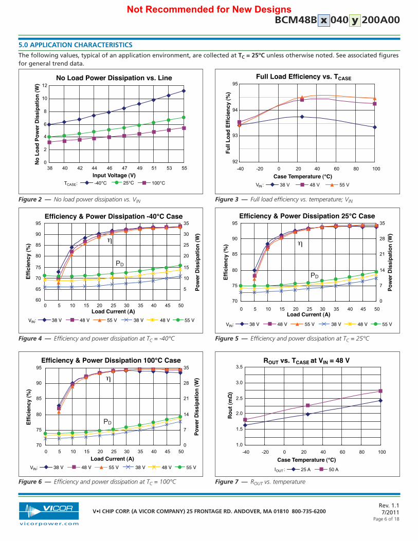
5.0 APPLICATION CHARACTERISTICS
The following values, typical of an application environment, are collected at TC = 25ºC unless otherwise noted. See associated figuresfor general trend data.
No Load Power Dissipation vs. Line
Input Voltage (V)
No
Lo
ad P
ow
er D
issi
pat
ion
(W
)
-40°C 100°CT :CASE 25°C
0
2
4
6
8
10
12
38 40 42 44 46 47 49 51 53 55
Full Load Efficiency vs. TCASE
Case Temperature (°C)
Fu
ll L
oad
Eff
icie
ncy
(%
)
38 V 48 V 55 VV :IN
92
93
94
95
-40 -20 0 20 40 60 80 100
Efficiency & Power Dissipation -40°C Case
Load Current (A)
Eff
icie
ncy
(%
)
38 V 48 V 55 VV :IN 38 V 48 V 55 V
Po
wer
Dis
sip
atio
n (
W)
60
65
70
75
80
85
90
95
0 5 10 15 20 25 30 35 40 45 50
5
10
15
20
25
30
35
η
PD
Figure 2 — No load power dissipation vs. VIN Figure 3 — Full load efficiency vs. temperature; VIN
Figure 4 — Efficiency and power dissipation at TC = -40°C
Efficiency & Power Dissipation 25°C Case
Load Current (A)
Eff
icie
ncy
(%
)
38 V 48 V 55 VV :IN 38 V 48 V 55 V
Po
wer
Dis
sip
atio
n (
W)
70
75
80
85
90
95
0 5 10 15 20 25 30 35 40 45 50
0
7
14
21
28
35
η
PD
Efficiency & Power Dissipation 100°C Case
Load Current (A)
Eff
icie
ncy
(%
)
38 V 48 V 55 VV :IN 38 V 48 V 55 V
Po
wer
Dis
sip
atio
n (
W)η
PD
70
75
80
85
90
95
0 5 10 15 20 25 30 35 40 45 500
7
14
21
28
35
Figure 5 — Efficiency and power dissipation at TC = 25°C
Figure 6 — Efficiency and power dissipation at TC = 100°C
ROUT vs. TCASE at VIN = 48 V
Case Temperature (°C)
�Ro
ut
(mΩ
)
I :OUT 25 A 50 A
1.0
1.5
2.0
2.5
3.0
3.5
-40 -20 0 20 40 60 80 100
Figure 7 — ROUT vs. temperature
Not Recommended for New Designs
Rev. 1.17/2011
Page 7 of 18
V•I CHIP CORP. (A VICOR COMPANY) 25 FRONTAGE RD. ANDOVER, MA 01810 800-735-6200
vicorpower.com
x 040 200A00yB48BCMPRELIMINARY DATASHEET
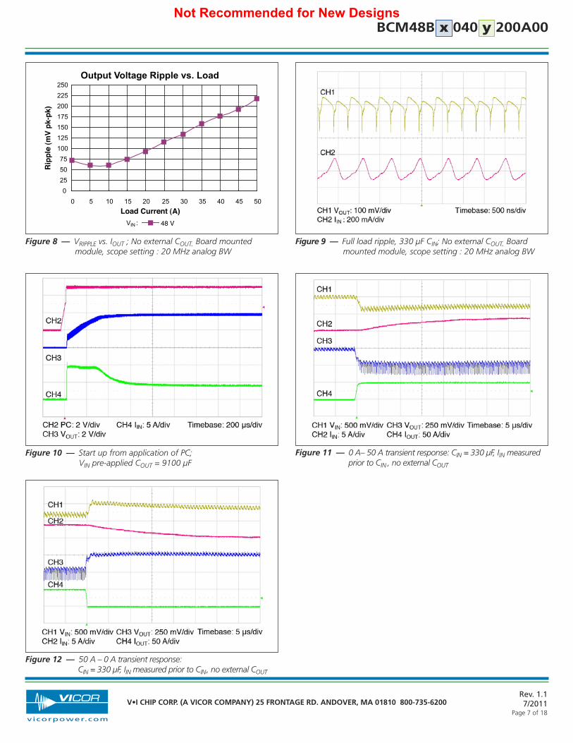
Figure 10 — Start up from application of PC; VIN pre-applied COUT = 9100 µF
Figure 9 — Full load ripple, 330 µF CIN; No external COUT. Board mounted module, scope setting : 20 MHz analog BW
Load Current (A)
Rip
ple
(m
V p
k-p
k)
48 VV :IN
Output Voltage Ripple vs. Load
0
25
50
75
100
125
150
175
200
225
250
0 5 10 15 20 25 30 35 40 45 50
Figure 8 — VRIPPLE vs. IOUT ; No external COUT. Board mounted module, scope setting : 20 MHz analog BW
Figure 12 — 50 A – 0 A transient response: CIN = 330 µF, IIN measured prior to CIN, no external COUT
Figure 11 — 0 A– 50 A transient response: CIN = 330 µF, IIN measured prior to CIN , no external COUT
Not Recommended for New Designs
Rev. 1.17/2011
Page 8 of 18
V•I CHIP CORP. (A VICOR COMPANY) 25 FRONTAGE RD. ANDOVER, MA 01810 800-735-6200
vicorpower.com
x 040 200A00yB48BCMPRELIMINARY DATASHEET
ATTRIBUTE SYMBOL CONDITIONS / NOTES MIN TYP MAX UNIT
MECHANICAL
Length L 32.25 / [1.270] 32.50 / [1.280] 32.75 / [1.289] mm/[in]
Width W 21.75 / [0.856] 22.00 / [0.866] 22.25 / [0.876] mm/[in]
Height H 6.48 / [0.255] 6.73 / [0.265] 6.98 / [0.275] mm/[in]
Volume Vol No heat sink 4.81 / [0.294] cm3/[in3]
Weight W 14.5 / [0.512] g/[oz]
Nickel 0.51 2.03
Lead finish Palladium 0.02 0.15 µm
Gold 0.003 0.051
THERMAL
BCM48BF040T200A00 (T-Grade) -40 125 °COperating temperature TJ
BCM48BF040M200A00 (M-Grade) -55 125 °C
Thermal resistance φJCIsothermal heatsink and
1 °C/Wisothermal internal PCB
Thermal capacity 5 Ws/°C
ASSEMBLY
Peak compressive forceSupported by J-lead only
6 lbsapplied to case (Z-axis) 5.41 lbs / in2
BCM48BF040T200A00 (T-Grade) -40 125 °CStorage temperature TST
BCM48BF040M200A00 (M-Grade) -65 125 °C
Moisture sensitivity level MSLMSL 6, 4 hours out of bag maximum
MSL 5
ESDHBMHuman Body Model,
1000"JEDEC JESD 22-A114D.01"Class 1D
ESD withstand
ESDCDMCharge Device Model,
400V
"JEDEC JESD 22-C101-D"
SOLDERING
Peak temperature during reflowMSL 6, 4 hours out of bag maximum 245 °C
MSL 5 225 °C
Peak time above 217°C 60 90 s
Peak heating rate during reflow 1.5 3 °C/s
Peak cooling rate post reflow 1.5 6 °C/s
SAFETY
Working voltage (IN – OUT) VIN_OUT 60 VDC
Isolation voltage (hipot) VHIPOT 2,250 VDC
Isolation capacitance CIN_OUT Unpowered unit 2500 3200 3800 pF
Isolation resistance RIN_OUT At 500 Vdc 10 MΩ
MTBF5.01 MHrs
6.55 MHrs
cTUVus
Agency approvals / standardscURusCE MarkRoHS 6 of 6
6.0 GENERAL CHARACTERISTICS
Specifications apply over all line and load conditions unless otherwise noted; Boldface specifications apply over the temperaturerange of -40ºC < TJ < 100ºC (T-Grade); All other specifications are at TJ = 25°C unless otherwise noted.
Telcordia Issue 2 - Method I Case III;25°C Ground Benign, Controlled
MIL-HDBK-217Plus Parts Count -25°C Ground Benign, Stationary,Indoors / Computer Profile
Not Recommended for New Designs
Rev. 1.17/2011
Page 9 of 18
V•I CHIP CORP. (A VICOR COMPANY) 25 FRONTAGE RD. ANDOVER, MA 01810 800-735-6200
vicorpower.com
x 040 200A00yB48BCMPRELIMINARY DATASHEET
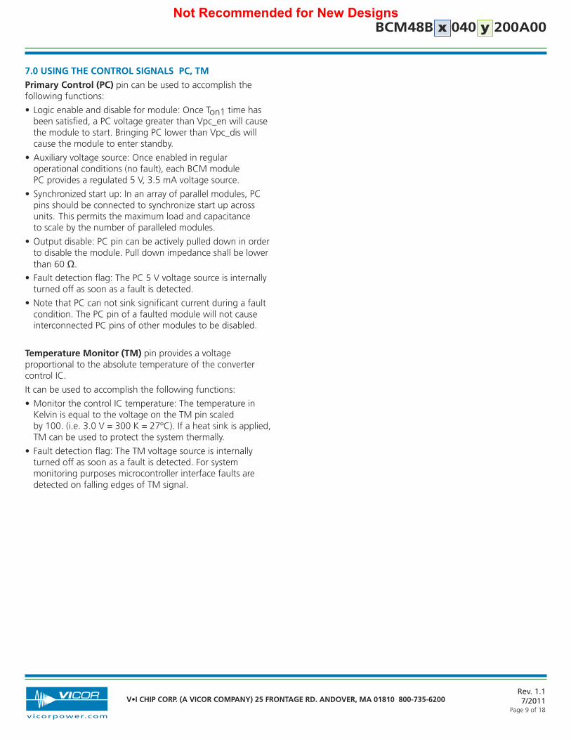
7.0 USING THE CONTROL SIGNALS PC, TM
Primary Control (PC) pin can be used to accomplish thefollowing functions:
• Logic enable and disable for module: Once Ton1 time has been satisfied, a PC voltage greater than Vpc_en will cause the module to start. Bringing PC lower than Vpc_dis will cause the module to enter standby.
• Auxiliary voltage source: Once enabled in regular operational conditions (no fault), each BCM modulePC provides a regulated 5 V, 3.5 mA voltage source.
• Synchronized start up: In an array of parallel modules, PC pins should be connected to synchronize start up across units. This permits the maximum load and capacitance to scale by the number of paralleled modules.
• Output disable: PC pin can be actively pulled down in order to disable the module. Pull down impedance shall be lower than 60 Ω.
• Fault detection flag: The PC 5 V voltage source is internally turned off as soon as a fault is detected.
• Note that PC can not sink significant current during a fault condition. The PC pin of a faulted module will not cause interconnected PC pins of other modules to be disabled.
Temperature Monitor (TM) pin provides a voltageproportional to the absolute temperature of the convertercontrol IC.
It can be used to accomplish the following functions:
• Monitor the control IC temperature: The temperature in Kelvin is equal to the voltage on the TM pin scaled by 100. (i.e. 3.0 V = 300 K = 27ºC). If a heat sink is applied, TM can be used to protect the system thermally.
• Fault detection flag: The TM voltage source is internally turned off as soon as a fault is detected. For system monitoring purposes microcontroller interface faults are detected on falling edges of TM signal.
Not Recommended for New Designs
Rev. 1.17/2011
Page 10 of 18
V•I CHIP CORP. (A VICOR COMPANY) 25 FRONTAGE RD. ANDOVER, MA 01810 800-735-6200
vicorpower.com
x 040 200A00yB48BCMPRELIMINARY DATASHEET
+V
out
-Vou
t
Mod
ulat
or
Fas
t cu
rren
tLi
mit S
low
curr
ent
limit
∫V
ref
TM
PC
Tem
pera
ture
depe
nde
nt v
olta
ge
sour
ce
Ena
ble
-Vin
2.5
V
100
uA
5 V
, 2 m
A m
in
150
K
40 K
1000
pF
18.5
V
3.1
V
Prim
ary
curr
ent
sens
ing
Tem
p_V
ref
Sta
rt u
p &
F
ault
logi
c
One
sho
t de
lay
Ton
1
“Wak
e-U
p” P
ower
An
d L
ogic
PC
Pu
ll-U
p&
Sou
rce
Ove
rtem
pera
ture
P
rote
ctio
n
Ove
rcur
rent
Pro
tect
ion
Ad
aptiv
e S
oft S
tart
Sec
ond
ary
Gat
e D
rive
UV
LOO
VLO
Vin
Vcc
V2
Vcc
Syn
chro
nou
s R
ectif
icat
ion
Prim
ary
Sta
ge
&
Res
ona
nt T
ank
Pow
erT
rans
form
er
Q1
Q2
Q6
Prim
ary
Gat
eD
rive
Q5
CO
UT
Q3
Q4
Gat
eD
rive
supp
ly
+V
in
0.01
F
1 K
LrC
r
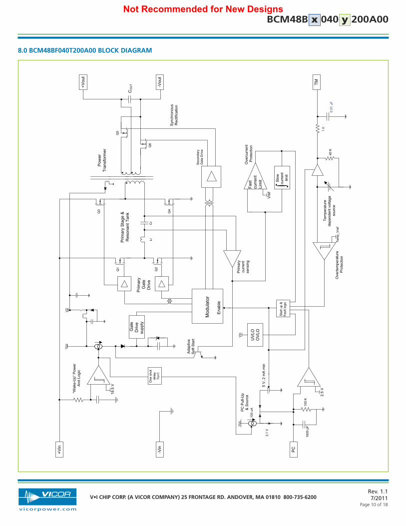
8.0 BCM48BF040T200A00 BLOCK DIAGRAM
Not Recommended for New Designs
Rev. 1.17/2011
Page 11 of 18
V•I CHIP CORP. (A VICOR COMPANY) 25 FRONTAGE RD. ANDOVER, MA 01810 800-735-6200
vicorpower.com
x 040 200A00yB48BCMPRELIMINARY DATASHEET
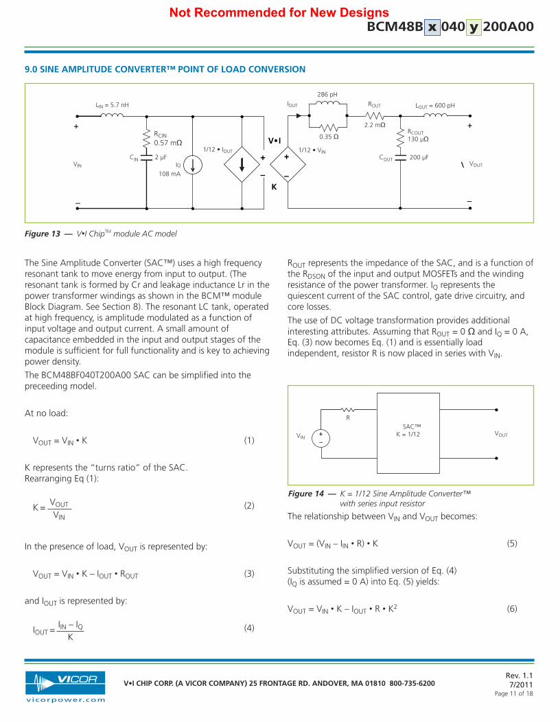
9.0 SINE AMPLITUDE CONVERTER™ POINT OF LOAD CONVERSION
The Sine Amplitude Converter (SAC™) uses a high frequencyresonant tank to move energy from input to output. (Theresonant tank is formed by Cr and leakage inductance Lr in thepower transformer windings as shown in the BCM™ moduleBlock Diagram. See Section 8). The resonant LC tank, operatedat high frequency, is amplitude modulated as a function ofinput voltage and output current. A small amount ofcapacitance embedded in the input and output stages of themodule is sufficient for full functionality and is key to achievingpower density.
The BCM48BF040T200A00 SAC can be simplified into thepreceeding model.
At no load:
VOUT = VIN • K (1)
K represents the “turns ratio” of the SAC. Rearranging Eq (1):
K =VOUT (2)VIN
In the presence of load, VOUT is represented by:
VOUT = VIN • K – IOUT • ROUT (3)
and IOUT is represented by:
IOUT =IIN – IQ (4)
K
ROUT represents the impedance of the SAC, and is a function ofthe RDSON of the input and output MOSFETs and the windingresistance of the power transformer. IQ represents thequiescent current of the SAC control, gate drive circuitry, andcore losses.
The use of DC voltage transformation provides additionalinteresting attributes. Assuming that ROUT = 0 Ω and IQ = 0 A,Eq. (3) now becomes Eq. (1) and is essentially loadindependent, resistor R is now placed in series with VIN.
The relationship between VIN and VOUT becomes:
VOUT = (VIN – IIN • R) • K (5)
Substituting the simplified version of Eq. (4) (IQ is assumed = 0 A) into Eq. (5) yields:
VOUT = VIN • K – IOUT • R • K2 (6)
+
–
+
–
VOUT
COUTVIN
V•I
K
+
–
+
–
CIN
IOUT
RCOUT
IQ
ROUT
RCIN
LIN = 5 nH
108 mA
1/12 • IOUT 1/12 • VIN
2.2 mΩRCIN0.57 mΩ
286 pH
0.35 Ω RCOUT130 µΩ
200 µF
LOUT = 600 pH
2 µFIQ
LIN = 5.7 nH IOUT ROUT
VIN VOUT
R
SACK = 1/32Vin
Vout+–
VINVOUT
RSAC™
K = 1/12
Figure 14 — K = 1/12 Sine Amplitude Converter™ with series input resistor
Figure 13 — V•I ChipTM module AC model
COUTCIN
Not Recommended for New Designs
Rev. 1.17/2011
Page 12 of 18
V•I CHIP CORP. (A VICOR COMPANY) 25 FRONTAGE RD. ANDOVER, MA 01810 800-735-6200
vicorpower.com
x 040 200A00yB48BCMPRELIMINARY DATASHEET
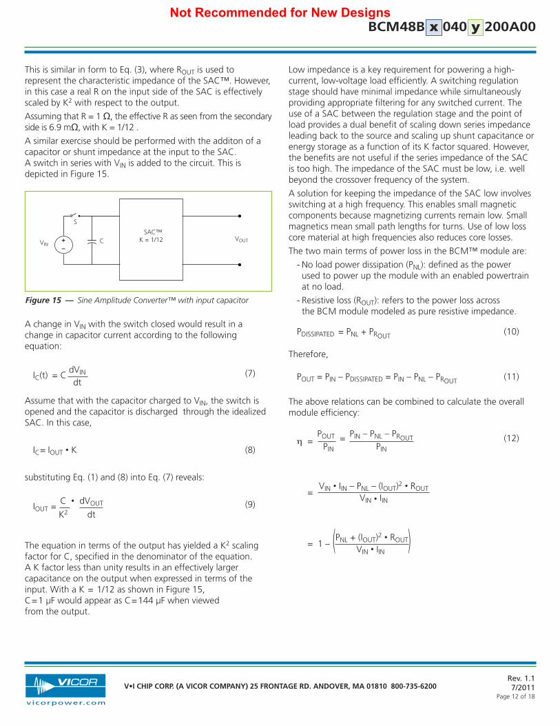
This is similar in form to Eq. (3), where ROUT is used torepresent the characteristic impedance of the SAC™. However,in this case a real R on the input side of the SAC is effectivelyscaled by K2 with respect to the output.
Assuming that R = 1Ω, the effective R as seen from the secondaryside is 6.9 mΩ, with K = 1/12 .
A similar exercise should be performed with the additon of acapacitor or shunt impedance at the input to the SAC. A switch in series with VIN is added to the circuit. This isdepicted in Figure 15.
A change in VIN with the switch closed would result in achange in capacitor current according to the followingequation:
IC(t) = CdVIN (7)dt
Assume that with the capacitor charged to VIN, the switch isopened and the capacitor is discharged through the idealizedSAC. In this case,
IC= IOUT • K (8)
substituting Eq. (1) and (8) into Eq. (7) reveals:
IOUT =C • dVOUT (9)K2 dt
The equation in terms of the output has yielded a K2 scalingfactor for C, specified in the denominator of the equation. A K factor less than unity results in an effectively largercapacitance on the output when expressed in terms of theinput. With a K = 1/12 as shown in Figure 15, C=1 µF would appear as C=144 µF when viewed from the output.
Low impedance is a key requirement for powering a high-current, low-voltage load efficiently. A switching regulationstage should have minimal impedance while simultaneouslyproviding appropriate filtering for any switched current. Theuse of a SAC between the regulation stage and the point ofload provides a dual benefit of scaling down series impedanceleading back to the source and scaling up shunt capacitance orenergy storage as a function of its K factor squared. However,the benefits are not useful if the series impedance of the SACis too high. The impedance of the SAC must be low, i.e. wellbeyond the crossover frequency of the system.
A solution for keeping the impedance of the SAC low involvesswitching at a high frequency. This enables small magneticcomponents because magnetizing currents remain low. Smallmagnetics mean small path lengths for turns. Use of low losscore material at high frequencies also reduces core losses.
The two main terms of power loss in the BCM™ module are:
- No load power dissipation (PNL): defined as the power used to power up the module with an enabled powertrainat no load.
- Resistive loss (ROUT): refers to the power loss across the BCM module modeled as pure resistive impedance.
PDISSIPATED = PNL + PROUT (10)
Therefore,
POUT = PIN – PDISSIPATED = PIN – PNL – PROUT (11)
The above relations can be combined to calculate the overallmodule efficiency:
η =POUT = PIN – PNL – PROUT (12)
PIN PIN
=VIN • IIN – PNL – (IOUT)2 • ROUT
VIN • IIN
= 1 – (PNL + (IOUT)2 • ROUT)VIN • IIN
C
S
SACK = 1/32Vin
Vout+–
VINVOUTC
SAC™K = 1/12
Figure 15 — Sine Amplitude Converter™ with input capacitor
S
Not Recommended for New Designs
Rev. 1.17/2011
Page 13 of 18
V•I CHIP CORP. (A VICOR COMPANY) 25 FRONTAGE RD. ANDOVER, MA 01810 800-735-6200
vicorpower.com
x 040 200A00yB48BCMPRELIMINARY DATASHEET
10.0 INPUT AND OUTPUT FILTER DESIGN
A major advantage of SAC™ systems versus conventionalPWM converters is that the transformers do not require large functional filters. The resonant LC tank, operated at extremehigh frequency, is amplitude modulated as a function of inputvoltage and output current and efficiently transfers chargethrough the isolation transformer. A small amount of capacitance embedded in the input and output stages of themodule is sufficient for full functionality and is key to achievepower density.
This paradigm shift requires system design to carefully evaluateexternal filters in order to:
1.Guarantee low source impedance:
To take full advantage of the BCM™ module’s dynamic response, the impedance presented to its input terminals must be low from DC to approximately 5 MHz. The connection of the bus converter module to its power source should be implemented with minimal distribution inductance. If the interconnect inductance exceeds 100 nH, the input should be bypassed with a RC damper to retain low source impedance and stable operation. With an interconnect inductance of 200 nH, the RC damper may be as high as 1 µF in series with 0.3 Ω. A single electrolytic or equivalent low-Q capacitor may be used in place of the series RC bypass.
2.Further reduce input and/or output voltage ripple without sacrificing dynamic response:
Given the wide bandwidth of the module, the source response is generally the limiting factor in the overall system response. Anomalies in the response of the source will appear at the output of the module multiplied by its K factor. This is illustrated in Figures 11 and 12.
3.Protect the module from overvoltage transients imposed by the system that would exceed maximum ratings and cause failures:
The module input/output voltage ranges shall not be exceeded. An internal overvoltage lockout function prevents operation outside of the normal operating input range. Even during this condition, the powertrain is exposedto the applied voltage and power MOSFETs must withstand it. A criterion for protection is the maximum amount of energy that the input or output switches can tolerate if avalanched.
Total load capacitance at the output of the BCM module shallnot exceed the specified maximum. Owing to the widebandwidth and low output impedance of the module, low-frequency bypass capacitance and significant energy
storage may be more densely and efficiently provided byadding capacitance at the input of the module. At frequencies<500 kHz the module appears as an impedance of ROUT
between the source and load.
Within this frequency range, capacitance at the input appearsas effective capacitance on the output per the relationship defined in Eq. 5.
COUT =CIN Eq. 6K2
This enables a reduction in the size and number of capacitorsused in a typical system.
11.0 THERMAL CONSIDERATIONS
V• I Chip™ products are multi-chip modules whosetemperature distribution varies greatly for each part number aswell as with the input / output conditions, thermalmanagement and environmental conditions. Maintaining thetop of the BCM48BF040T200A00 case to less than 100ºC willkeep all junctions within the V• I Chip module below 125ºC formost applications.
The percent of total heat dissipated through the top surfaceversus through the J-lead is entirely dependent on theparticular mechanical and thermal environment. The heatdissipated through the top surface is typically 60%. The heatdissipated through the J-lead onto the PCB surface is typically40%. Use 100% top surface dissipation when designing for aconservative cooling solution.
It is not recommended to use a V• I Chip module for anextended period of time at full load without proper heat sinking.
Not Recommended for New Designs
Rev. 1.17/2011
Page 14 of 18
V•I CHIP CORP. (A VICOR COMPANY) 25 FRONTAGE RD. ANDOVER, MA 01810 800-735-6200
vicorpower.com
x 040 200A00yB48BCMPRELIMINARY DATASHEET
BCM1
R0_1
ZIN_EQ1 ZOUT_EQ1
ZOUT_EQ2
Vout
ZOUT_EQn
ZIN_EQ2
ZIN_EQn
R0_2
R0_n
BCM2
BCMn
LoadDC
Vin
+
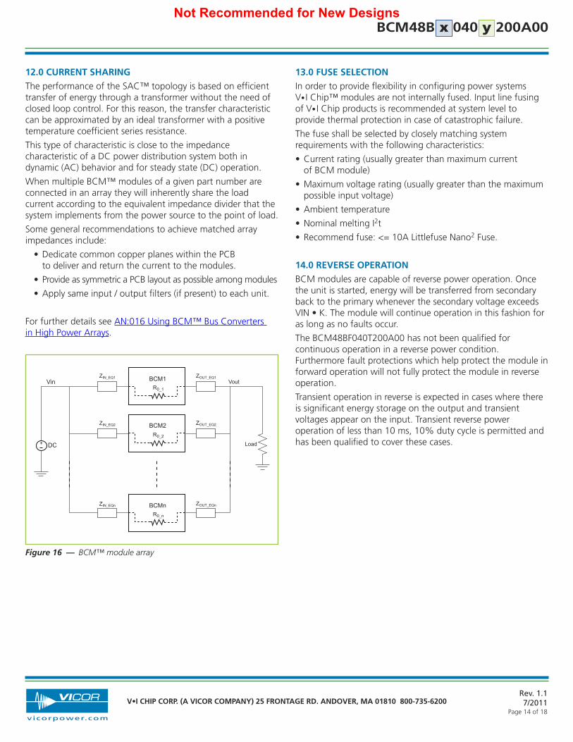
Figure 16 — BCM™ module array
12.0 CURRENT SHARING
The performance of the SAC™ topology is based on efficienttransfer of energy through a transformer without the need ofclosed loop control. For this reason, the transfer characteristiccan be approximated by an ideal transformer with a positivetemperature coefficient series resistance.
This type of characteristic is close to the impedancecharacteristic of a DC power distribution system both indynamic (AC) behavior and for steady state (DC) operation.
When multiple BCM™ modules of a given part number areconnected in an array they will inherently share the loadcurrent according to the equivalent impedance divider that thesystem implements from the power source to the point of load.
Some general recommendations to achieve matched arrayimpedances include:
• Dedicate common copper planes within the PCB to deliver and return the current to the modules.
• Provide as symmetric a PCB layout as possible among modules
• Apply same input / output filters (if present) to each unit.
For further details see AN:016 Using BCM™ Bus Converters in High Power Arrays.
13.0 FUSE SELECTION
In order to provide flexibility in configuring power systems V• I Chip™ modules are not internally fused. Input line fusing of V• I Chip products is recommended at system level toprovide thermal protection in case of catastrophic failure.
The fuse shall be selected by closely matching system requirements with the following characteristics:
• Current rating (usually greater than maximum current of BCM module)
• Maximum voltage rating (usually greater than the maximum possible input voltage)
• Ambient temperature
• Nominal melting I2t
• Recommend fuse: <= 10A Littlefuse Nano2 Fuse.
14.0 REVERSE OPERATION
BCM modules are capable of reverse power operation. Oncethe unit is started, energy will be transferred from secondaryback to the primary whenever the secondary voltage exceedsVIN • K. The module will continue operation in this fashion foras long as no faults occur.
The BCM48BF040T200A00 has not been qualified forcontinuous operation in a reverse power condition.Furthermore fault protections which help protect the module inforward operation will not fully protect the module in reverseoperation.
Transient operation in reverse is expected in cases where thereis significant energy storage on the output and transientvoltages appear on the input. Transient reverse poweroperation of less than 10 ms, 10% duty cycle is permitted andhas been qualified to cover these cases.
Not Recommended for New Designs
Rev. 1.17/2011
Page 15 of 18
V•I CHIP CORP. (A VICOR COMPANY) 25 FRONTAGE RD. ANDOVER, MA 01810 800-735-6200
vicorpower.com
x 040 200A00yB48BCMPRELIMINARY DATASHEET
inchmmNOTES:
1. DIMENSIONS ARE .2. UNLESS OTHERWISE SPECIFIED, TOLERANCES ARE: .X / [.XX] = +/-0.25 / [.01]; .XX / [.XXX] = +/-0.13 / [.005]3. PRODUCT MARKING ON TOP SURFACE
DXF and PDF files are available on vicorpower.com
inchmmNOTES:
1. DIMENSIONS ARE .2. UNLESS OTHERWISE SPECIFIED, TOLERANCES ARE: .X / [.XX] = +/-0.25 / [.01]; .XX / [.XXX] = +/-0.13 / [.005]3. PRODUCT MARKING ON TOP SURFACE
DXF and PDF files are available on vicorpower.com
15.2 J-LEAD PACKAGE RECOMMENDED LAND PATTERN
mm(inch)
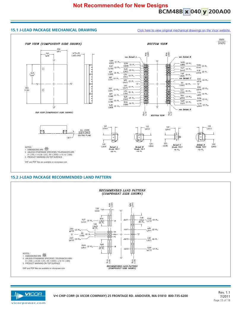
15.1 J-LEAD PACKAGE MECHANICAL DRAWING Click here to view original mechanical drawings on the Vicor website.
Not Recommended for New Designs
Rev. 1.17/2011
Page 16 of 18
V•I CHIP CORP. (A VICOR COMPANY) 25 FRONTAGE RD. ANDOVER, MA 01810 800-735-6200
vicorpower.com
x 040 200A00yB48BCMPRELIMINARY DATASHEET
TOP VIEW ( COMPONENT SIDE )
BOTTOM VIEWNOTES: 1. DIMENSIONS ARE
2. UNLESS OTHERWISE SPECIFIED TOLERANCES ARE: X.X [X.XX] = ±0.25 [0.01]; X.XX [X.XXX] = ±0.13 [0.005]
3. RoHS COMPLIANT PER CST-0001 LATEST REVISION
DXF and PDF files are available on vicorpower.com
inch(mm)
.
NOTES: 1. DIMENSIONS ARE
2. UNLESS OTHERWISE SPECIFIED TOLERANCES ARE: X.X [X.XX] = ±0.25 [0.01]; X.XX [X.XXX] = ±0.13 [0.005]
3. RoHS COMPLIANT PER CST-0001 LATEST REVISION
DXF and PDF files are available on vicorpower.com
inch(mm)
.
RECOMMENDED HOLE PATTERN( COMPONENT SIDE SHOWN )
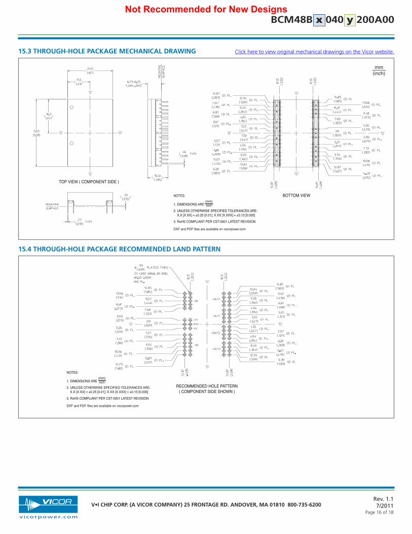
15.4 THROUGH-HOLE PACKAGE RECOMMENDED LAND PATTERN
mm(inch)
15.3 THROUGH-HOLE PACKAGE MECHANICAL DRAWING Click here to view original mechanical drawings on the Vicor website.
Not Recommended for New Designs
Rev. 1.17/2011
Page 17 of 18
V•I CHIP CORP. (A VICOR COMPANY) 25 FRONTAGE RD. ANDOVER, MA 01810 800-735-6200
vicorpower.com
x 040 200A00yB48BCMPRELIMINARY DATASHEET
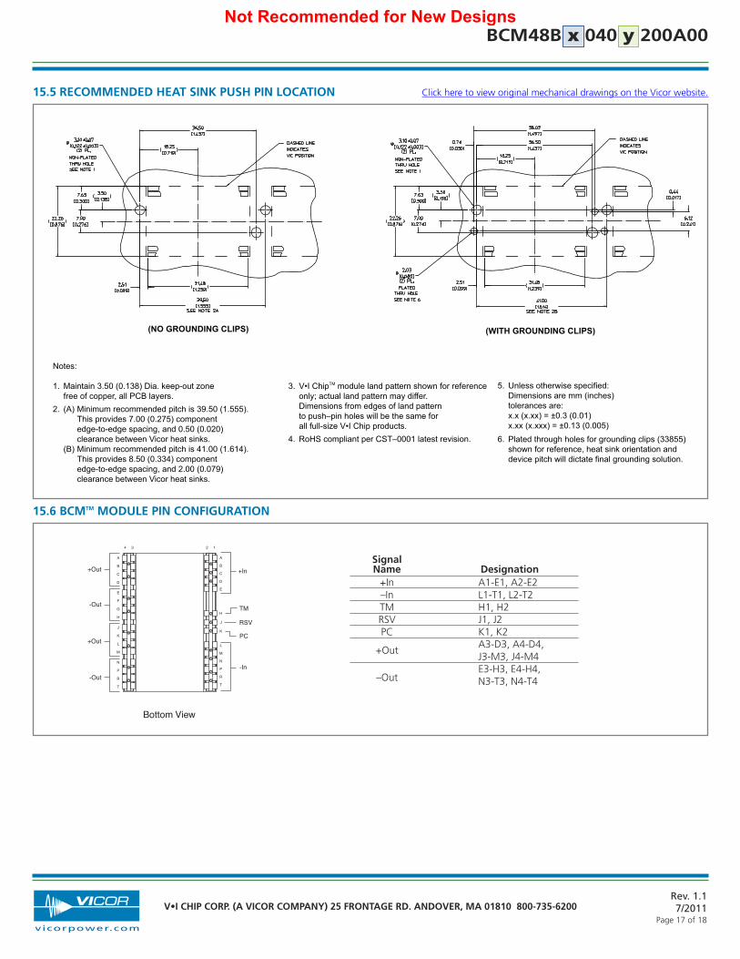
Notes:
1. Maintain 3.50 (0.138) Dia. keep-out zone free of copper, all PCB layers.
2. (A) Minimum recommended pitch is 39.50 (1.555). This provides 7.00 (0.275) component edge-to-edge spacing, and 0.50 (0.020) clearance between Vicor heat sinks. (B) Minimum recommended pitch is 41.00 (1.614). This provides 8.50 (0.334) component edge-to-edge spacing, and 2.00 (0.079) clearance between Vicor heat sinks.
3. V•I ChipTM module land pattern shown for reference only; actual land pattern may differ. Dimensions from edges of land pattern to push–pin holes will be the same for all full-size V•I Chip products.
4. RoHS compliant per CST–0001 latest revision.
(NO GROUNDING CLIPS) (WITH GROUNDING CLIPS)
5. Unless otherwise specified: Dimensions are mm (inches) tolerances are: x.x (x.xx) = ±0.3 (0.01) x.xx (x.xxx) = ±0.13 (0.005)
6. Plated through holes for grounding clips (33855) shown for reference, heat sink orientation and device pitch will dictate final grounding solution.
15.5 RECOMMENDED HEAT SINK PUSH PIN LOCATION
-In
PC
RSV
TM
+In
-Out
+Out
-Out
+Out
Bottom View
A
B
C
D
E
F
G
H
J
K
L
M
N
P
R
T
4 3 2 1
A
B
C
D
E
H
J
K
L
M
N
P
R
T
15.6 BCMTM MODULE PIN CONFIGURATION
Click here to view original mechanical drawings on the Vicor website.
Signal Name Designation
+In A1-E1, A2-E2–In L1-T1, L2-T2TM H1, H2RSV J1, J2PC K1, K2
+OutA3-D3, A4-D4,J3-M3, J4-M4
–OutE3-H3, E4-H4,N3-T3, N4-T4
Not Recommended for New Designs

Rev. 1.17/2011
Page 18 of 18
V•I CHIP CORP. (A VICOR COMPANY) 25 FRONTAGE RD. ANDOVER, MA 01810 800-735-6200
vicorpower.com
x 040 200A00yB48BCMPRELIMINARY DATASHEET
Vicor’s comprehensive line of power solutions includes high density AC-DCand DC-DC modules and accessory components, fully configurable AC-DCand DC-DC power supplies, and complete custom power systems.
Information furnished by Vicor is believed to be accurate and reliable. However, no responsibility is assumed by Vicor forits use. Vicor components are not designed to be used in applications, such as life support systems, wherein a failure ormalfunction could result in injury or death. All sales are subject to Vicor’s Terms and Conditions of Sale, which are available upon request.
Specifications are subject to change without notice.
Intellectual Property Notice
Vicor and its subsidiaries own Intellectual Property (including issued U.S. and Foreign Patents and pending patentapplications) relating to the products described in this data sheet. Interested parties should contact Vicor'sIntellectual Property Department.
The products described on this data sheet are protected by the following U.S. Patents Numbers:5,945,130; 6,403,009; 6,710,257; 6,911,848; 6,930,893; 6,934,166; 6,940,013; 6,969,909; 7,038,917;7,145,186; 7,166,898; 7,187,263; 7,202,646; 7,361,844; D496,906; D505,114; D506,438; D509,472; and foruse under 6,975,098 and 6,984,965.
Vicor Corporation25 Frontage Road
Andover, MA, USA 01810Tel: 800-735-6200Fax: 978-475-6715
emailCustomer Service: [email protected]
Technical Support: [email protected]
WarrantyVicor products are guaranteed for two years from date of shipment against defects in material or workmanship when innormal use and service. This warranty does not extend to products subjected to misuse, accident, or improperapplication or maintenance. Vicor shall not be liable for collateral or consequential damage. This warranty is extended tothe original purchaser only.
EXCEPT FOR THE FOREGOING EXPRESS WARRANTY, VICOR MAKES NO WARRANTY, EXPRESS OR IMPLIED, INCLUDING,BUT NOT LIMITED TO, THE WARRANTY OF MERCHANTABILITY OR FITNESS FOR A PARTICULAR PURPOSE.
Vicor will repair or replace defective products in accordance with its own best judgement. For service under thiswarranty, the buyer must contact Vicor to obtain a Return Material Authorization (RMA) number and shippinginstructions. Products returned without prior authorization will be returned to the buyer. The buyer will pay all chargesincurred in returning the product to the factory. Vicor will pay all reshipment charges if the product was defective withinthe terms of this warranty.
Information published by Vicor has been carefully checked and is believed to be accurate; however, no responsibility isassumed for inaccuracies. Vicor reserves the right to make changes to any products without further notice to improvereliability, function, or design. Vicor does not assume any liability arising out of the application or use of any product orcircuit; neither does it convey any license under its patent rights nor the rights of others. Vicor general policy does notrecommend the use of its components in life support applications wherein a failure or malfunction may directly threatenlife or injury. Per Vicor Terms and Conditions of Sale, the user of Vicor components in life support applications assumesall risks of such use and indemnifies Vicor against all damages.
Not Recommended for New Designs
Top Related