


γλώσσες
Σελίδες
Νομικός

Document No. U16961EJ4V0UD00 (4th edition) Date Published September 2006 NS CP(K)
Printed in Japan
μPD78F0112H μPD78F0113H μPD78F0114H μPD78F0114HD μPD78F0112H(A) μPD78F0113H(A) μPD78F0114H(A) μPD78F0112H(A1) μPD78F0113H(A1) μPD78F0114H(A1)
78K0/KC1+ 8-Bit Single-Chip Microcontrollers
User’s Manual
2004

User’s Manual U16961EJ4V0UD 2
[MEMO]
User’s Manual U16961EJ4V0UD 3
1
2
3
4
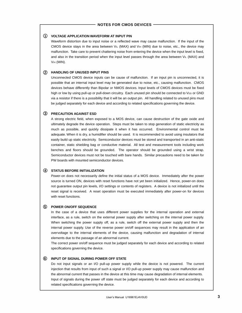
VOLTAGE APPLICATION WAVEFORM AT INPUT PIN
Waveform distortion due to input noise or a reflected wave may cause malfunction. If the input of the
CMOS device stays in the area between VIL (MAX) and VIH (MIN) due to noise, etc., the device may
malfunction. Take care to prevent chattering noise from entering the device when the input level is fixed,
and also in the transition period when the input level passes through the area between VIL (MAX) and
VIH (MIN).
HANDLING OF UNUSED INPUT PINS
Unconnected CMOS device inputs can be cause of malfunction. If an input pin is unconnected, it is
possible that an internal input level may be generated due to noise, etc., causing malfunction. CMOS
devices behave differently than Bipolar or NMOS devices. Input levels of CMOS devices must be fixed
high or low by using pull-up or pull-down circuitry. Each unused pin should be connected to VDD or GND
via a resistor if there is a possibility that it will be an output pin. All handling related to unused pins must
be judged separately for each device and according to related specifications governing the device.
PRECAUTION AGAINST ESD
A strong electric field, when exposed to a MOS device, can cause destruction of the gate oxide and
ultimately degrade the device operation. Steps must be taken to stop generation of static electricity as
much as possible, and quickly dissipate it when it has occurred. Environmental control must be
adequate. When it is dry, a humidifier should be used. It is recommended to avoid using insulators that
easily build up static electricity. Semiconductor devices must be stored and transported in an anti-static
container, static shielding bag or conductive material. All test and measurement tools including work
benches and floors should be grounded. The operator should be grounded using a wrist strap.
Semiconductor devices must not be touched with bare hands. Similar precautions need to be taken for
PW boards with mounted semiconductor devices.
STATUS BEFORE INITIALIZATION
Power-on does not necessarily define the initial status of a MOS device. Immediately after the power
source is turned ON, devices with reset functions have not yet been initialized. Hence, power-on does
not guarantee output pin levels, I/O settings or contents of registers. A device is not initialized until the
reset signal is received. A reset operation must be executed immediately after power-on for devices
with reset functions.
POWER ON/OFF SEQUENCE
In the case of a device that uses different power supplies for the internal operation and external
interface, as a rule, switch on the external power supply after switching on the internal power supply.
When switching the power supply off, as a rule, switch off the external power supply and then the
internal power supply. Use of the reverse power on/off sequences may result in the application of an
overvoltage to the internal elements of the device, causing malfunction and degradation of internal
elements due to the passage of an abnormal current.
The correct power on/off sequence must be judged separately for each device and according to related
specifications governing the device.
INPUT OF SIGNAL DURING POWER OFF STATE
Do not input signals or an I/O pull-up power supply while the device is not powered. The current
injection that results from input of such a signal or I/O pull-up power supply may cause malfunction and
the abnormal current that passes in the device at this time may cause degradation of internal elements.
Input of signals during the power off state must be judged separately for each device and according to
related specifications governing the device.
NOTES FOR CMOS DEVICES
5
6
User’s Manual U16961EJ4V0UD 4
Windows and Windows NT are either registered trademarks or trademarks of Microsoft Corporation in the United States and/or other countries. PC/AT is a trademark of International Business Machines Corporation. HP9000 series 700 and HP-UX are trademarks of Hewlett-Packard Company. SPARCstation is a trademark of SPARC International, Inc. Solaris and SunOS are trademarks of Sun Microsystems, Inc. SuperFlash is a registered trademark of Silicon Storage Technology, Inc. in several countries including the United States and Japan.
Caution: This product uses SuperFlash® technology licensed from Silicon Storage Technology, inc.
The information in this document is current as of August, 2006. The information is subject to change without notice. For actual design-in, refer to the latest publications of NEC Electronics data sheets or data books, etc., for the most up-to-date specifications of NEC Electronics products. Not all products and/or types are available in every country. Please check with an NEC Electronics sales representative for availability and additional information.No part of this document may be copied or reproduced in any form or by any means without the prior written consent of NEC Electronics. NEC Electronics assumes no responsibility for any errors that may appear in this document.NEC Electronics does not assume any liability for infringement of patents, copyrights or other intellectual property rights of third parties by or arising from the use of NEC Electronics products listed in this document or any other liability arising from the use of such products. No license, express, implied or otherwise, is granted under any patents, copyrights or other intellectual property rights of NEC Electronics or others.Descriptions of circuits, software and other related information in this document are provided for illustrative purposes in semiconductor product operation and application examples. The incorporation of these circuits, software and information in the design of a customer's equipment shall be done under the full responsibility of the customer. NEC Electronics assumes no responsibility for any losses incurred by customers or third parties arising from the use of these circuits, software and information.While NEC Electronics endeavors to enhance the quality, reliability and safety of NEC Electronics products, customers agree and acknowledge that the possibility of defects thereof cannot be eliminated entirely. To minimize risks of damage to property or injury (including death) to persons arising from defects in NEC Electronics products, customers must incorporate sufficient safety measures in their design, such as redundancy, fire-containment and anti-failure features.NEC Electronics products are classified into the following three quality grades: "Standard", "Special" and "Specific". The "Specific" quality grade applies only to NEC Electronics products developed based on a customer-designated "quality assurance program" for a specific application. The recommended applications of an NEC Electronics product depend on its quality grade, as indicated below. Customers must check the quality grade of each NEC Electronics product before using it in a particular application.
The quality grade of NEC Electronics products is "Standard" unless otherwise expressly specified in NEC Electronics data sheets or data books, etc. If customers wish to use NEC Electronics products in applications not intended by NEC Electronics, they must contact an NEC Electronics sales representative in advance to determine NEC Electronics' willingness to support a given application.
(Note)
•
•
•
•
•
•
M8E 02. 11-1
(1)
(2)
"NEC Electronics" as used in this statement means NEC Electronics Corporation and also includes its majority-owned subsidiaries."NEC Electronics products" means any product developed or manufactured by or for NEC Electronics (as defined above).
Computers, office equipment, communications equipment, test and measurement equipment, audioand visual equipment, home electronic appliances, machine tools, personal electronic equipmentand industrial robots.Transportation equipment (automobiles, trains, ships, etc.), traffic control systems, anti-disastersystems, anti-crime systems, safety equipment and medical equipment (not specifically designedfor life support).Aircraft, aerospace equipment, submersible repeaters, nuclear reactor control systems, lifesupport systems and medical equipment for life support, etc.
"Standard":
"Special":
"Specific":
User’s Manual U16961EJ4V0UD 5
INTRODUCTION Readers This manual is intended for user engineers who wish to understand the functions of the
78K0/KC1+ and design and develop application systems and programs for these devices.
The target products are as follows. 78K0/KC1+: μPD78F0112H, 78F0113H, 78F0114H, 78F0112H(A), 78F0113H(A),
78F0114H(A), 78F0112H(A1), 78F0113H(A1), 78F0114H(A1), 78F0114HD Purpose This manual is intended to give users an understanding of the functions described in the
Organization below. Organization The 78K0/KC1+ manual is separated into two parts: this manual and the instructions
edition (common to the 78K/0 Series).
78K0/KC1+ User’s Manual (This Manual)
78K/0 Series User’s Manual Instructions
• Pin functions • Internal block functions • Interrupts • Other on-chip peripheral functions • Electrical specifications
• CPU functions • Instruction set • Explanation of each instruction
How to Read This Manual It is assumed that the readers of this manual have general knowledge of electrical
engineering, logic circuits, and microcontrollers.
• When using this manual as the manual for (A) grade products and (A1) grade products:
→ Only the quality grade differs between standard products and (A), (A1) grade products. Read the part number as follows.
• μPD78F0112H → μPD78F0112H(A), 78F0112H(A1) • To gain a general understanding of functions: → Read this manual in the order of the CONTENTS. The mark <R> shows major
revised points. The revised points can be easily searched by copying an "<R>" in the PDF file and specifying it in the "Find what:" field.
• How to interpret the register format: → For a bit number enclosed in brackets, the bit name is defined as a reserved word
in the RA78K0, and is defined as an sfr variable by #pragma sfr directive in the CC78K0.
• To check the details of a register when you know the register name: → Refer to APPENDIX C REGISTER INDEX. • To know details of the 78K/0 Series instructions: → Refer to the separate document 78K/0 Series Instructions User’s Manual
(U12326E).
User’s Manual U16961EJ4V0UD 6
Caution Examples in this manual employ the “standard” quality grade for general electronics. When using examples in this manual for the “special” quality grade, review the quality grade of each part and/or circuit actually used.
Conventions Data significance: Higher digits on the left and lower digits on the right Active low representations: ××× (overscore over pin and signal name) Note: Footnote for item marked with Note in the text. Caution: Information requiring particular attention Remark: Supplementary information Numerical representations: Binary ...×××× or ××××B Decimal ...×××× Hexadecimal ...××××H Differences Between 78K0/KC1+ and 78K0/KC1
Series Name Item
78K0/KC1+ 78K0/KC1
Mask ROM version None Available
Power supply Single power supply Two power supplies
Self-programming function Available None
Flash memory version
Option byte Internal oscillator can be stopped/cannot be stopped selectable
None
RC oscillation (3 to 4 MHz) Available None
Power-on clear (POC) function 2.1 V ±0.1 V (fixed) 2.85 V ±0.15 V or 3.5 V ±0.2 V selectable
Version with on-chip debug function Available (μPD78F0114HD) None
Minimum instruction execution time 0.125 μs (at 16 MHz operation) 0.166 μs (at 12 MHz operation)
User’s Manual U16961EJ4V0UD 7
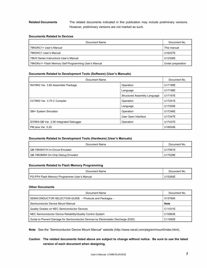
Related Documents The related documents indicated in this publication may include preliminary versions. However, preliminary versions are not marked as such.
Documents Related to Devices
Document Name Document No.
78K0/KC1+ User’s Manual This manual
78K0/KC1 User’s Manual U16227E
78K/0 Series Instructions User’s Manual U12326E
78K0/Kx1+ Flash Memory Self Programming User’s Manual Under preparation
Documents Related to Development Tools (Software) (User’s Manuals)
Document Name Document No.
Operation U17199E
Language U17198E
RA78K0 Ver. 3.80 Assembler Package
Structured Assembly Language U17197E
Operation U17201E CC78K0 Ver. 3.70 C Compiler
Language U17200E
Operation U17246E SM+ System Simulator
User Open Interface U17247E
ID78K0-QB Ver. 2.90 Integrated Debugger Operation U17437E
PM plus Ver. 5.20 U16934E
Documents Related to Development Tools (Hardware) (User’s Manuals)
Document Name Document No.
QB-78K0KX1H In-Circuit Emulator U17081E
QB-78K0MINI On-Chip Debug Emulator U17029E
Documents Related to Flash Memory Programming
Document Name Document No.
PG-FP4 Flash Memory Programmer User’s Manual U15260E
Other Documents
Document Name Document No.
SEMICONDUCTOR SELECTION GUIDE − Products and Packages − X13769X
Semiconductor Device Mount Manual Note
Quality Grades on NEC Semiconductor Devices C11531E
NEC Semiconductor Device Reliability/Quality Control System C10983E
Guide to Prevent Damage for Semiconductor Devices by Electrostatic Discharge (ESD) C11892E
Note See the “Semiconductor Device Mount Manual” website (http://www.necel.com/pkg/en/mount/index.html). Caution The related documents listed above are subject to change without notice. Be sure to use the latest
version of each document when designing.
User’s Manual U16961EJ4V0UD 8
CONTENTS
CHAPTER 1 OUTLINE............................................................................................................................. 15 1.1 Features.......................................................................................................................................... 15 1.2 Applications ................................................................................................................................... 16 1.3 Ordering Information..................................................................................................................... 17 1.4 Pin Configuration (Top View) ....................................................................................................... 18 1.5 Kx1 Series Lineup ......................................................................................................................... 20
1.5.1 78K0/Kx1, 78K0/Kx1+ product lineup................................................................................................ 20 1.5.2 V850ES/Kx1, V850ES/Kx1+ product lineup ...................................................................................... 23
1.6 Block Diagram ............................................................................................................................... 26 1.7 Outline of Functions...................................................................................................................... 27
CHAPTER 2 PIN FUNCTIONS ............................................................................................................... 29 2.1 Pin Function List ........................................................................................................................... 29 2.2 Description of Pin Functions ....................................................................................................... 33
2.2.1 P00 and P01 (port 0) ......................................................................................................................... 33 2.2.2 P10 to P17 (port 1) ............................................................................................................................ 34 2.2.3 P20 to P27 (port 2) ............................................................................................................................ 35 2.2.4 P30 to P33 (port 3) ............................................................................................................................ 35 2.2.5 P60 to P63 (port 6) ............................................................................................................................ 35 2.2.6 P70 to P73 (port 7) ............................................................................................................................ 36 2.2.7 P120 (port 12) ................................................................................................................................... 36 2.2.8 P130 (port 13) ................................................................................................................................... 36 2.2.9 AVREF................................................................................................................................................ 36 2.2.10 AVSS................................................................................................................................................ 36 2.2.11 RESET ............................................................................................................................................ 36 2.2.12 X1 and X2........................................................................................................................................ 36 2.2.13 CL1 and CL2 ................................................................................................................................... 37 2.2.14 XT1 and XT2 ................................................................................................................................... 37 2.2.15 VDD and EVDD ................................................................................................................................. 37 2.2.16 VSS and EVSS.................................................................................................................................. 37 2.2.17 FLMD0 and FLMD1......................................................................................................................... 37
2.3 Pin I/O Circuits and Recommended Connection of Unused Pins ............................................ 38
CHAPTER 3 CPU ARCHITECTURE ...................................................................................................... 42 3.1 Memory Space ............................................................................................................................... 42
3.1.1 Internal program memory space........................................................................................................ 47 3.1.2 Internal data memory space .............................................................................................................. 48 3.1.3 Special function register (SFR) area ................................................................................................. 48 3.1.4 Data memory addressing .................................................................................................................. 49
3.2 Processor Registers...................................................................................................................... 53 3.2.1 Control registers ................................................................................................................................ 53 3.2.2 General-purpose registers................................................................................................................. 57 3.2.3 Special function registers (SFRs) ...................................................................................................... 58
3.3 Instruction Address Addressing.................................................................................................. 62 3.3.1 Relative addressing........................................................................................................................... 62
User’s Manual U16961EJ4V0UD 9
3.3.2 Immediate addressing........................................................................................................................63 3.3.3 Table indirect addressing ...................................................................................................................64 3.3.4 Register addressing ...........................................................................................................................64
3.4 Operand Address Addressing ..................................................................................................... 65 3.4.1 Implied addressing .............................................................................................................................65 3.4.2 Register addressing ...........................................................................................................................66 3.4.3 Direct addressing ...............................................................................................................................67 3.4.4 Short direct addressing ......................................................................................................................68 3.4.5 Special function register (SFR) addressing........................................................................................69 3.4.6 Register indirect addressing...............................................................................................................70 3.4.7 Based addressing ..............................................................................................................................71 3.4.8 Based indexed addressing.................................................................................................................72 3.4.9 Stack addressing................................................................................................................................73
CHAPTER 4 PORT FUNCTIONS........................................................................................................... 74 4.1 Port Functions............................................................................................................................... 74 4.2 Port Configuration ........................................................................................................................ 76
4.2.1 Port 0 .................................................................................................................................................77 4.2.2 Port 1 .................................................................................................................................................79 4.2.3 Port 2 .................................................................................................................................................84 4.2.4 Port 3 .................................................................................................................................................85 4.2.5 Port 6 .................................................................................................................................................87 4.2.6 Port 7 .................................................................................................................................................88 4.2.7 Port 12 ...............................................................................................................................................89 4.2.8 Port 13 ...............................................................................................................................................90
4.3 Registers Controlling Port Function ........................................................................................... 91 4.4 Port Function Operations............................................................................................................. 95
4.4.1 Writing to I/O port ...............................................................................................................................95 4.4.2 Reading from I/O port.........................................................................................................................95 4.4.3 Operations on I/O port........................................................................................................................95
CHAPTER 5 CLOCK GENERATOR ...................................................................................................... 96 5.1 Functions of Clock Generator...................................................................................................... 96 5.2 Configuration of Clock Generator ............................................................................................... 96 5.3 Registers Controlling Clock Generator ...................................................................................... 98 5.4 System Clock Oscillator ............................................................................................................. 105
5.4.1 High-speed system clock oscillator ..................................................................................................105 5.4.2 Subsystem clock oscillator ...............................................................................................................106 5.4.3 Example of incorrect resonator connection ......................................................................................107 5.4.4 When subsystem clock is not used ..................................................................................................110 5.4.5 Internal oscillator ..............................................................................................................................110 5.4.6 Prescaler..........................................................................................................................................110
5.5 Clock Generator Operation ........................................................................................................ 111 5.6 Time Required to Switch Between Internal Oscillation Clock and High-Speed
System Clock........................................................................................................................... 118 5.7 Time Required for CPU Clock Switchover................................................................................ 119 5.8 Clock Switching Flowchart and Register Setting .................................................................... 120
5.8.1 Switching from internal oscillation clock to high-speed system clock ...............................................120
User’s Manual U16961EJ4V0UD 10
5.8.2 Switching from high-speed system clock to internal oscillation clock .............................................. 121 5.8.3 Switching from high-speed system clock to subsystem clock.......................................................... 122 5.8.4 Switching from subsystem clock to high-speed system clock.......................................................... 123 5.8.5 Register settings.............................................................................................................................. 124
CHAPTER 6 16-BIT TIMER/EVENT COUNTER 00 ........................................................................... 125 6.1 Functions of 16-Bit Timer/Event Counter 00 ............................................................................ 125 6.2 Configuration of 16-Bit Timer/Event Counter 00...................................................................... 126 6.3 Registers Controlling 16-Bit Timer/Event Counter 00 ............................................................. 130 6.4 Operation of 16-Bit Timer/Event Counter 00 ............................................................................ 136
6.4.1 Interval timer operation.................................................................................................................... 136 6.4.2 PPG output operations .................................................................................................................... 138 6.4.3 Pulse width measurement operations ............................................................................................. 141 6.4.4 External event counter operation..................................................................................................... 149 6.4.5 Square-wave output operation ........................................................................................................ 151 6.4.6 One-shot pulse output operation ..................................................................................................... 153
6.5 Cautions for 16-Bit Timer/Event Counter 00............................................................................. 158
CHAPTER 7 8-BIT TIMER/EVENT COUNTERS 50 AND 51........................................................... 161 7.1 Functions of 8-Bit Timer/Event Counters 50 and 51................................................................ 161 7.2 Configuration of 8-Bit Timer/Event Counters 50 and 51 ......................................................... 163 7.3 Registers Controlling 8-Bit Timer/Event Counters 50 and 51................................................. 165 7.4 Operations of 8-Bit Timer/Event Counters 50 and 51 .............................................................. 170
7.4.1 Operation as interval timer .............................................................................................................. 170 7.4.2 Operation as external event counter ............................................................................................... 172 7.4.3 Square-wave output operation ........................................................................................................ 173 7.4.4 PWM output operation..................................................................................................................... 174
7.5 Cautions for 8-Bit Timer/Event Counters 50 and 51 ................................................................ 178
CHAPTER 8 8-BIT TIMERS H0 AND H1 .......................................................................................... 179 8.1 Functions of 8-Bit Timers H0 and H1 ........................................................................................ 179 8.2 Configuration of 8-Bit Timers H0 and H1.................................................................................. 179 8.3 Registers Controlling 8-Bit Timers H0 and H1 ......................................................................... 183 8.4 Operation of 8-Bit Timers H0 and H1......................................................................................... 189
8.4.1 Operation as interval timer/square-wave output .............................................................................. 189 8.4.2 Operation as PWM output mode ..................................................................................................... 192 8.4.3 Carrier generator mode operation (8-bit timer H1 only) ................................................................... 198
CHAPTER 9 WATCH TIMER................................................................................................................ 205 9.1 Functions of Watch Timer .......................................................................................................... 205 9.2 Configuration of Watch Timer.................................................................................................... 207 9.3 Register Controlling Watch Timer ............................................................................................. 207 9.4 Watch Timer Operations............................................................................................................. 209
9.4.1 Watch timer operation ..................................................................................................................... 209 9.4.2 Interval timer operation.................................................................................................................... 210
9.5 Cautions for Watch Timer........................................................................................................... 211
CHAPTER 10 WATCHDOG TIMER ..................................................................................................... 212 10.1 Functions of Watchdog Timer.................................................................................................. 212
User’s Manual U16961EJ4V0UD 11
10.2 Configuration of Watchdog Timer........................................................................................... 214 10.3 Registers Controlling Watchdog Timer .................................................................................. 214 10.4 Operation of Watchdog Timer.................................................................................................. 217
10.4.1 Watchdog timer operation when “internal oscillator cannot be stopped” is selected by option byte................................................................................................................................................217
10.4.2 Watchdog timer operation when “internal oscillator can be stopped by software” is selected by option byte .....................................................................................................................................218
10.4.3 Watchdog timer operation in STOP mode (when “internal oscillator can be stopped by software” is selected by option byte).................................................................................................................219
10.4.4 Watchdog timer operation in HALT mode (when “internal oscillator can be stopped by software” is selected by option byte).................................................................................................................221
CHAPTER 11 A/D CONVERTER ......................................................................................................... 222 11.1 Functions of A/D Converter ..................................................................................................... 222 11.2 Configuration of A/D Converter ............................................................................................... 223 11.3 Registers Used in A/D Converter ............................................................................................ 225 11.4 A/D Converter Operations ........................................................................................................ 230
11.4.1 Basic operations of A/D converter..................................................................................................230 11.4.2 Input voltage and conversion results..............................................................................................232 11.4.3 A/D converter operation mode .......................................................................................................233
11.5 How to Read A/D Converter Characteristics Table................................................................ 236 11.6 Cautions for A/D Converter...................................................................................................... 238
CHAPTER 12 SERIAL INTERFACE UART0...................................................................................... 243 12.1 Functions of Serial Interface UART0....................................................................................... 243 12.2 Configuration of Serial Interface UART0 ................................................................................ 244 12.3 Registers Controlling Serial Interface UART0........................................................................ 247 12.4 Operation of Serial Interface UART0....................................................................................... 252
12.4.1 Operation stop mode......................................................................................................................252 12.4.2 Asynchronous serial interface (UART) mode .................................................................................253 12.4.3 Dedicated baud rate generator.......................................................................................................259
CHAPTER 13 SERIAL INTERFACE UART6...................................................................................... 264 13.1 Functions of Serial Interface UART6....................................................................................... 264 13.2 Configuration of Serial Interface UART6 ................................................................................ 268 13.3 Registers Controlling Serial Interface UART6........................................................................ 271 13.4 Operation of Serial Interface UART6....................................................................................... 280
13.4.1 Operation stop mode......................................................................................................................280 13.4.2 Asynchronous serial interface (UART) mode .................................................................................281 13.4.3 Dedicated baud rate generator.......................................................................................................295
CHAPTER 14 SERIAL INTERFACE CSI10 ........................................................................................ 302 14.1 Functions of Serial Interface CSI10......................................................................................... 302 14.2 Configuration of Serial Interface CSI10 .................................................................................. 302 14.3 Registers Controlling Serial Interface CSI10.......................................................................... 304 14.4 Operation of Serial Interface CSI10......................................................................................... 307
14.4.1 Operation stop mode......................................................................................................................307 14.4.2 3-wire serial I/O mode ....................................................................................................................308
User’s Manual U16961EJ4V0UD 12
CHAPTER 15 INTERRUPT FUNCTIONS............................................................................................. 316 15.1 Interrupt Function Types .......................................................................................................... 316 15.2 Interrupt Sources and Configuration ...................................................................................... 316 15.3 Registers Controlling Interrupt Functions.............................................................................. 319 15.4 Interrupt Servicing Operations ................................................................................................ 326
15.4.1 Maskable interrupt request acknowledgment ................................................................................ 326 15.4.2 Software interrupt request acknowledgment ................................................................................. 328 15.4.3 Multiple interrupt servicing............................................................................................................. 329 15.4.4 Interrupt request hold .................................................................................................................... 332
CHAPTER 16 KEY INTERRUPT FUNCTION ..................................................................................... 333 16.1 Functions of Key Interrupt ....................................................................................................... 333 16.2 Configuration of Key Interrupt ................................................................................................. 333 16.3 Register Controlling Key Interrupt .......................................................................................... 334
CHAPTER 17 STANDBY FUNCTION .................................................................................................. 335 17.1 Standby Function and Configuration...................................................................................... 335
17.1.1 Standby function............................................................................................................................ 335 17.1.2 Registers controlling standby function........................................................................................... 337
17.2 Standby Function Operation .................................................................................................... 339 17.2.1 HALT mode ................................................................................................................................... 339 17.2.2 STOP mode................................................................................................................................... 344
CHAPTER 18 RESET FUNCTION........................................................................................................ 348 18.1 Register for Confirming Reset Source.................................................................................... 354
CHAPTER 19 CLOCK MONITOR ........................................................................................................ 355 19.1 Functions of Clock Monitor...................................................................................................... 355 19.2 Configuration of Clock Monitor ............................................................................................... 355 19.3 Register Controlling Clock Monitor......................................................................................... 356 19.4 Operation of Clock Monitor ...................................................................................................... 357
CHAPTER 20 POWER-ON-CLEAR CIRCUIT...................................................................................... 362 20.1 Functions of Power-on-Clear Circuit....................................................................................... 362 20.2 Configuration of Power-on-Clear Circuit ................................................................................ 363 20.3 Operation of Power-on-Clear Circuit ....................................................................................... 363 20.4 Cautions for Power-on-Clear Circuit ....................................................................................... 364
CHAPTER 21 LOW-VOLTAGE DETECTOR ....................................................................................... 366 21.1 Functions of Low-Voltage Detector......................................................................................... 366 21.2 Configuration of Low-Voltage Detector .................................................................................. 366 21.3 Registers Controlling Low-Voltage Detector.......................................................................... 367 21.4 Operation of Low-Voltage Detector ......................................................................................... 370 21.5 Cautions for Low-Voltage Detector ......................................................................................... 374
CHAPTER 22 OPTION BYTE............................................................................................................... 378 22.1 Functions of Option Bytes ....................................................................................................... 378 22.2 Format of Option Byte .............................................................................................................. 378
User’s Manual U16961EJ4V0UD 13
CHAPTER 23 FLASH MEMORY.......................................................................................................... 381 23.1 Internal Memory Size Switching Register............................................................................... 382 23.2 Writing with Flash Programmer............................................................................................... 383 23.3 Programming Environment...................................................................................................... 388 23.4 Communication Mode............................................................................................................... 388 23.5 Handling of Pins on Board....................................................................................................... 391
23.5.1 FLMD0 pin .....................................................................................................................................391 23.5.2 FLMD1 pin .....................................................................................................................................391 23.5.3 Serial interface pins........................................................................................................................392 23.5.4 RESET pin .....................................................................................................................................394 23.5.5 Port pins.........................................................................................................................................394 23.5.6 Other signal pins ............................................................................................................................394 23.5.7 Power supply..................................................................................................................................394
23.6 Programming Method ............................................................................................................... 395 23.6.1 Controlling flash memory ...............................................................................................................395 23.6.2 Flash memory programming mode ................................................................................................395 23.6.3 Selecting communication mode .....................................................................................................396 23.6.4 Communication commands............................................................................................................397
23.7 Flash Memory Programming by Self-Writing ......................................................................... 398 23.7.1 Registers used for self-programming function................................................................................399
23.8 Boot Swap Function ................................................................................................................. 403 23.8.1 Outline of boot swap function .........................................................................................................403 23.8.2 Memory map and boot area ...........................................................................................................404
CHAPTER 24 ON-CHIP DEBUG FUNCTION (μPD78F0114HD ONLY).......................................... 408 24.1 On-Chip Debug Security ID ...................................................................................................... 409
CHAPTER 25 INSTRUCTION SET ...................................................................................................... 410 25.1 Conventions Used in Operation List....................................................................................... 410
25.1.1 Operand identifiers and specification methods...............................................................................410 25.1.2 Description of operation column.....................................................................................................411 25.1.3 Description of flag operation column ..............................................................................................411
25.2 Operation List ............................................................................................................................ 412 25.3 Instructions Listed by Addressing Type ................................................................................ 420
CHAPTER 26 ELECTRICAL SPECIFICATIONS (STANDARD PRODUCTS, (A) GRADE PRODUCTS) .................................................................................................................. 423
CHAPTER 27 ELECTRICAL SPECIFICATIONS ((A1) GRADE PRODUCTS)................................ 441
CHAPTER 28 PACKAGE DRAWING .................................................................................................. 457
CHAPTER 29 RECOMMENDED SOLDERING CONDITIONS........................................................... 458
CHAPTER 30 CAUTIONS FOR WAIT ................................................................................................ 459 30.1 Cautions for Wait ...................................................................................................................... 459 30.2 Peripheral Hardware That Generates Wait ............................................................................. 460 30.3 Example of Wait Occurrence ................................................................................................... 461
User’s Manual U16961EJ4V0UD 14
APPENDIX A DEVELOPMENT TOOLS............................................................................................... 462 A.1 Software Package ....................................................................................................................... 465 A.2 Language Processing Software ................................................................................................ 465 A.3 Control Software ......................................................................................................................... 466 A.4 Flash Memory Writing Tools...................................................................................................... 466 A.5 Debugging Tools (Hardware)..................................................................................................... 467
A.5.1 When using in-circuit emulator QB-78K0KX1H............................................................................... 467 A.5.2 When using on-chip debug emulator QB-78K0MINI ....................................................................... 468
A.6 Debugging Tools (Software)...................................................................................................... 468
APPENDIX B NOTES ON TARGET SYSTEM DESIGN ................................................................... 469
APPENDIX C REGISTER INDEX ......................................................................................................... 470 C.1 Register Index (In Alphabetical Order with Respect to Register Names) ............................. 470 C.2 Register Index (In Alphabetical Order with Respect to Register Symbol)............................ 473
APPENDIX D LIST OF CAUTIONS..................................................................................................... 476
APPENDIX E REVISION HISTORY...................................................................................................... 502 E.1 Major Revisions in This Edition................................................................................................. 502 E.2 Revision History up to Previous Edition .................................................................................. 502
User’s Manual U16961EJ4V0UD 15
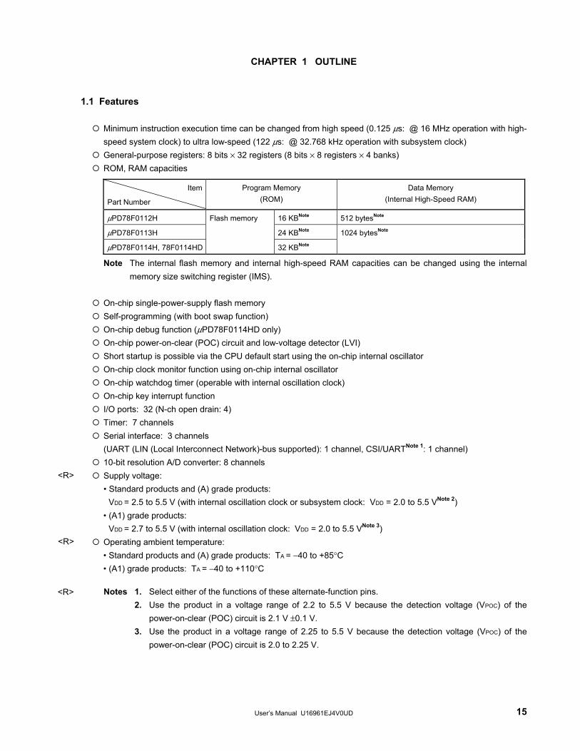
CHAPTER 1 OUTLINE 1.1 Features
Minimum instruction execution time can be changed from high speed (0.125 μs: @ 16 MHz operation with high-speed system clock) to ultra low-speed (122 μs: @ 32.768 kHz operation with subsystem clock)
General-purpose registers: 8 bits × 32 registers (8 bits × 8 registers × 4 banks) ROM, RAM capacities
Item
Part Number
Program Memory (ROM)
Data Memory (Internal High-Speed RAM)
μPD78F0112H 16 KBNote 512 bytesNote
μPD78F0113H 24 KBNote
μPD78F0114H, 78F0114HD
Flash memory
32 KBNote
1024 bytesNote
Note The internal flash memory and internal high-speed RAM capacities can be changed using the internal memory size switching register (IMS).
On-chip single-power-supply flash memory Self-programming (with boot swap function) On-chip debug function (μPD78F0114HD only) On-chip power-on-clear (POC) circuit and low-voltage detector (LVI) Short startup is possible via the CPU default start using the on-chip internal oscillator On-chip clock monitor function using on-chip internal oscillator On-chip watchdog timer (operable with internal oscillation clock) On-chip key interrupt function I/O ports: 32 (N-ch open drain: 4) Timer: 7 channels Serial interface: 3 channels
(UART (LIN (Local Interconnect Network)-bus supported): 1 channel, CSI/UARTNote 1: 1 channel) 10-bit resolution A/D converter: 8 channels Supply voltage: • Standard products and (A) grade products:
VDD = 2.5 to 5.5 V (with internal oscillation clock or subsystem clock: VDD = 2.0 to 5.5 VNote 2) • (A1) grade products:
VDD = 2.7 to 5.5 V (with internal oscillation clock: VDD = 2.0 to 5.5 VNote 3) Operating ambient temperature: • Standard products and (A) grade products: TA = −40 to +85°C • (A1) grade products: TA = −40 to +110°C
Notes 1. Select either of the functions of these alternate-function pins. 2. Use the product in a voltage range of 2.2 to 5.5 V because the detection voltage (VPOC) of the
power-on-clear (POC) circuit is 2.1 V ±0.1 V. 3. Use the product in a voltage range of 2.25 to 5.5 V because the detection voltage (VPOC) of the
power-on-clear (POC) circuit is 2.0 to 2.25 V.
<R>
<R>
<R>
CHAPTER 1 OUTLINE
User’s Manual U16961EJ4V0UD 16
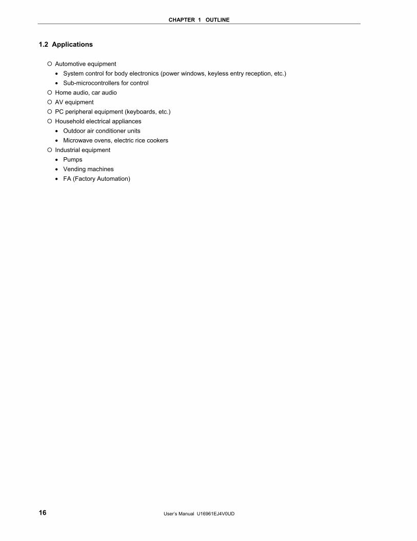
1.2 Applications
Automotive equipment • System control for body electronics (power windows, keyless entry reception, etc.) • Sub-microcontrollers for control
Home audio, car audio AV equipment PC peripheral equipment (keyboards, etc.) Household electrical appliances
• Outdoor air conditioner units • Microwave ovens, electric rice cookers
Industrial equipment • Pumps • Vending machines • FA (Factory Automation)

CHAPTER 1 OUTLINE
User’s Manual U16961EJ4V0UD 17
1.3 Ordering Information
• Flash memory version
Part Number Package Quality Grade μPD78F0112HGB-8ES 44-pin plastic LQFP (10 × 10) Standard μPD78F0112HGB-8ES-A 44-pin plastic LQFP (10 × 10) Standard μPD78F0113HGB-8ES 44-pin plastic LQFP (10 × 10) Standard μPD78F0113HGB-8ES-A 44-pin plastic LQFP (10 × 10) Standard μPD78F0114HGB-8ES 44-pin plastic LQFP (10 × 10) Standard μPD78F0114HGB-8ES-A 44-pin plastic LQFP (10 × 10) Standard μPD78F0114HDGB-8ES Note 44-pin plastic LQFP (10 × 10) Standard μPD78F0112HGB(A)-8ES 44-pin plastic LQFP (10 × 10) Special μPD78F0112HGB(A)-8ES-A 44-pin plastic LQFP (10 × 10) Special μPD78F0113HGB(A)-8ES 44-pin plastic LQFP (10 × 10) Special μPD78F0113HGB(A)-8ES-A 44-pin plastic LQFP (10 × 10) Special μPD78F0114HGB(A)-8ES 44-pin plastic LQFP (10 × 10) Special μPD78F0114HGB(A)-8ES-A 44-pin plastic LQFP (10 × 10) Special μPD78F0112HGB(A1)-8ES 44-pin plastic LQFP (10 × 10) Special μPD78F0112HGB(A1)-8ES-A 44-pin plastic LQFP (10 × 10) Special μPD78F0113HGB(A1)-8ES 44-pin plastic LQFP (10 × 10) Special μPD78F0113HGB(A1)-8ES-A 44-pin plastic LQFP (10 × 10) Special μPD78F0114HGB(A1)-8ES 44-pin plastic LQFP (10 × 10) Special μPD78F0114HGB(A1)-8ES-A 44-pin plastic LQFP (10 × 10) Special
Note Only the ES (emulation sample) version is available. Use this product for program evaluation. Remark Products that have the part numbers suffixed by "-A" are lead-free products.
Please re fer to "Qual i ty Grades on NEC Semiconductor Dev ices" (Document No. C11531E) pub l i shed byNEC Electronics Corporat ion to know the speci f icat ion of the qual i ty grade on the device and i ts recommended applications.
<R>
CHAPTER 1 OUTLINE
User’s Manual U16961EJ4V0UD 18
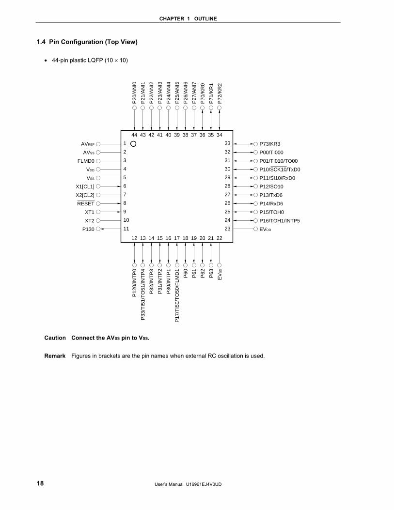
1.4 Pin Configuration (Top View)
• 44-pin plastic LQFP (10 × 10)
1
2
3
4
5
6
7
8
9
10
11
33
32
31
30
29
28
27
26
25
24
23
AVREF
AVSS
FLMD0
VDD
VSS
X1[CL1]
X2[CL2]
RESET
XT1
XT2
P130
P73/KR3
P00/TI000
P01/TI010/TO00
P10/SCK10/TxD0
P11/SI10/RxD0
P12/SO10
P13/TxD6
P14/RxD6
P15/TOH0
P16/TOH1/INTP5
EVDD
12 13 14 15 16 17 18 19 20 21 22
44 43 42 41 40 39 38 37 36 35 34P
120/
INT
P0
P33
/TI5
1/T
O51
/INT
P4
P32
/INT
P3
P31
/INT
P2
P30
/INT
P1
P17
/TI5
0/T
O50
/FLM
D1
P60
P61
P62
P63
EV
SS
P20
/AN
I0
P21
/AN
I1
P22
/AN
I2
P23
/AN
I3
P24
/AN
I4
P25
/AN
I5
P26
/AN
I6
P27
/AN
I7
P70
/KR
0
P71
/KR
1
P72
/KR
2
Caution Connect the AVSS pin to VSS.
Remark Figures in brackets are the pin names when external RC oscillation is used.
CHAPTER 1 OUTLINE
User’s Manual U16961EJ4V0UD 19
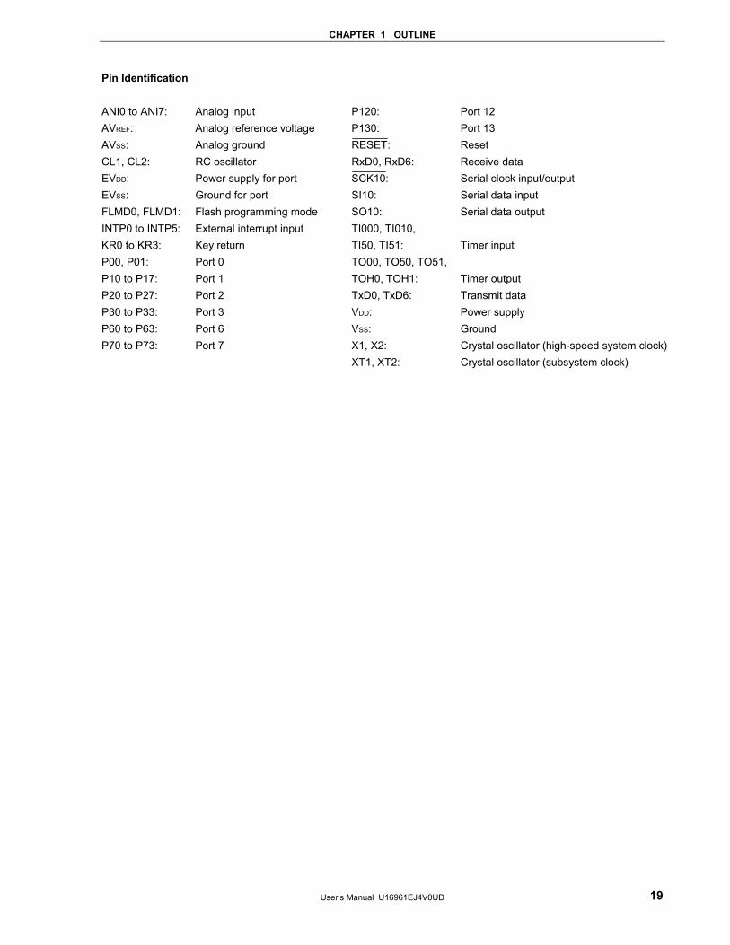
Pin Identification ANI0 to ANI7: Analog input AVREF: Analog reference voltage AVSS: Analog ground CL1, CL2: RC oscillator EVDD: Power supply for port EVSS: Ground for port FLMD0, FLMD1: Flash programming mode INTP0 to INTP5: External interrupt input KR0 to KR3: Key return P00, P01: Port 0 P10 to P17: Port 1 P20 to P27: Port 2 P30 to P33: Port 3 P60 to P63: Port 6 P70 to P73: Port 7
P120: Port 12 P130: Port 13 RESET: Reset RxD0, RxD6: Receive data SCK10: Serial clock input/output SI10: Serial data input SO10: Serial data output TI000, TI010, TI50, TI51: Timer input TO00, TO50, TO51, TOH0, TOH1: Timer output TxD0, TxD6: Transmit data VDD: Power supply VSS: Ground X1, X2: Crystal oscillator (high-speed system clock) XT1, XT2: Crystal oscillator (subsystem clock)
CHAPTER 1 OUTLINE
User’s Manual U16961EJ4V0UD 20
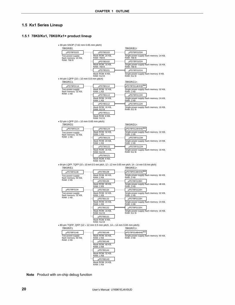
1.5 Kx1 Series Lineup 1.5.1 78K0/Kx1, 78K0/Kx1+ product lineup
Mask ROM: 24 KB, RAM: 768 B
Mask ROM: 16 KB, RAM: 768 B
Mask ROM: 8 KB, RAM: 512 B
PD780101
78K0/KB1• 30-pin SSOP (7.62 mm 0.65 mm pitch)
Single-power-supply flash memory: 24 KB, RAM: 768 B
Single-power-supply flash memory: 16 KB, RAM: 768 B
Single-power-supply flash memory: 8 KB, RAM: 512 B
PD780102
PD780103PD78F0103
Two-power-supply flash memory: 24 KB, RAM: 768 B
78K0/KB1+
PD78F0102H
PD78F0103H
PD78F0101H
• 44-pin LQFP (10 × 10 mm 0.8 mm pitch)
PD78F0114
Two-power-supply flash memory: 32 KB, RAM: 1 KB
Mask ROM: 32 KB, RAM: 1 KB
PD780114
Mask ROM: 24 KB, RAM: 1 KB
PD780113
Mask ROM: 16 KB, RAM: 512 B
PD780112
PD780111
78K0/KC1
Single-power-supply flash memory: 32 KB, RAM: 1 KB
Single-power-supply flash memory: 24 KB, RAM: 1 KB
Single-power-supply flash memory: 16 KB, RAM: 512 B
78K0/KC1+
PD78F0113H
PD78F0114H/HDNote
PD78F0112H
Mask ROM: 8 KB, RAM: 512 B
PD78F0124
Mask ROM: 32 KB, RAM: 1 KB
PD780124
Mask ROM: 24 KB, RAM: 1 KB
PD780123
Mask ROM: 16 KB, RAM: 512 B
PD780122
Mask ROM: 8 KB, RAM: 512 B
PD780121
• 52-pin LQFP (10 × 10 mm 0.65 mm pitch)
Single-power-supply flash memory: 32 KB, RAM: 1 KB
Single-power-supply flash memory: 24 KB, RAM: 1 KB
Single-power-supply flash memory: 16 KB, RAM: 512 B
78K0/KD1+
PD78F0123H
PD78F0124H/HDNote
PD78F0122H
Two-power-supply flash memory: 32 KB, RAM: 1 KB
PD78F0148
Mask ROM: 60 KB, RAM: 2 KB
PD780148
Mask ROM: 48 KB, RAM: 2 KB
PD780146
Mask ROM: 32 KB, RAM: 1 KB
PD780144
Mask ROM: 24 KB, RAM: 1 KB
PD780143
• 80-pin TQFP, QFP (12 × 12 mm 0.5 mm pitch, 14 × 14 mm 0.65 mm pitch)
Single-power-supply flash memory: 60 KB, RAM: 2 KB
78K0/KF1+
PD78F0148H/HDNote
78K0/KF1
Two-power-supply flash memory: 60 KB, RAM: 2 KB
PD78F0138 PD780138
PD780136
• 64-pin LQFP, TQFP (10 × 10 mm 0.5 mm pitch, 12 × 12 mm 0.65 mm pitch, 14 × 14 mm 0.8 mm pitch)78K0/KE1+
PD78F0136H
PD78F0138H/HDNote
78K0/KE1
PD78F0134
Mask ROM: 32 KB, RAM: 1 KB
PD780134
Mask ROM: 24 KB, RAM: 1 KB
PD780133
Mask ROM: 16 KB, RAM: 512 B
PD780132
Mask ROM: 8 KB, RAM: 512 B
PD780131
Single-power-supply flash memory: 32 KB, RAM: 1 KB
Single-power-supply flash memory: 24 KB, RAM: 1 KB
Single-power-supply flash memory: 16 KB, RAM: 512 B
PD78F0133H
PD78F0134H
PD78F0132H
Two-power-supply flash memory: 32 KB, RAM: 1 KB
Mask ROM: 60 KB, RAM: 2 KB
Mask ROM: 48 KB, RAM: 2 KB
Single-power-supply flash memory: 60 KB, RAM: 2 KB
Single-power-supply flash memory: 48 KB, RAM: 2 KB
Two-power-supply flash memory: 60 KB, RAM: 2 KB
μ μ μ
μ μ
μ μ
μ μ
μ
μ
μ
μ
μ
μ
μ μ
μ
μ
μ
μ
μ
μ
μ
μ
μ
μ
μ
μ
μ
μ
μ
μ
μ
μ
μ
μ μ
μ
μ
μ
μ
78K0/KD1
Note Product with on-chip debug function
CHAPTER 1 OUTLINE
User’s Manual U16961EJ4V0UD 21
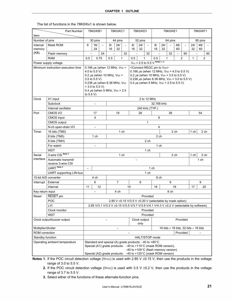
The list of functions in the 78K0/Kx1 is shown below.
Part Number Item
78K0/KB1 78K0/KC1 78K0/KD1 78K0/KE1 78K0/KF1
Number of pins 30 pins 44 pins 52 pins 64 pins 80 pins Mask ROM 8 16/
24 − 8/
16 24/32
− 8/16
24/32
− 8/16
24/ 32
− 48/ 60
− 24/32
48/60
−
Flash memory − 24 − 32 − 32 − 32 − 60 − 60
Internal memory (KB)
RAM 0.5 0.75 0.5 1 0.5 1 0.5 1 2 1 2 Power supply voltage VDD = 2.5 to 5.5 V Notes 1, 2 Minimum instruction execution time 0.166 μs (when 12 MHz, VDD =
4.0 to 5.5 V) 0.2 μs (when 10 MHz, VDD = 3.5 to 5.5 V) 0.238 μs (when 8.38 MHz, VDD = 3.0 to 5.5 V) 0.4 μs (when 5 MHz, VDD = 2.5 to 5.5 V)
<Connect REGC pin to VDD> 0.166 μs (when 12 MHz, VDD = 4.0 to 5.5 V) 0.2 μs (when 10 MHz, VDD = 3.5 to 5.5 V) 0.238 μs (when 8.38 MHz, VDD = 3.0 to 5.5 V) 0.4 μs (when 5 MHz, VDD = 2.5 to 5.5 V)
X1 input 2 to 12 MHz Subclock − 32.768 kHz
Clock
Internal oscillator 240 kHz (TYP.) CMOS I/O 17 19 26 38 54 CMOS input 4 8 CMOS output 1
Port
N-ch open-drain I/O − 4 16 bits (TM0) 1 ch 2 ch 1 ch 2 ch 8 bits (TM5) 1 ch 2 ch 8 bits (TMH) 2 ch For watch − 1 ch
Timer
WDT 1 ch 3-wire CSI Note 3 1 ch 2 ch 1 ch 2 ch Automatic transmit/ receive 3-wire CSI
− 1 ch
UART Note 3 − 1 ch
Serial interface
UART supporting LIN-bus 1 ch 10-bit A/D converter 4 ch 8 ch
External 6 7 8 9 9 Interrupt Internal 11 12 15 16 19 17 20
Key return input − 4 ch 8 ch RESET pin Provided POC 2.85 V ±0.15 V/3.5 V ±0.20 V (selectable by mask option) LVI 2.85 V/3.1 V/3.3 V ±0.15 V/3.5 V/3.7 V/3.9 V/4.1 V/4.3 V ±0.2 V (selectable by software) Clock monitor Provided
Reset
WDT Provided Clock output/buzzer output − Clock output
only Provided
Multiplier/divider − 16 bits × 16 bits, 32 bits ÷ 16 bits ROM correction − Provided − Standby function HALT/STOP mode Operating ambient temperature Standard and special (A) grade products: −40 to +85°C
Special (A1) grade products: −40 to +110°C (mask ROM version), −40 to +105°C (flash memory version) Special (A2) grade products: −40 to +125°C (mask ROM version)
Notes 1. If the POC circuit detection voltage (VPOC) is used with 2.85 V ±0.15 V, then use the products in the voltage range of 3.0 to 5.5 V.
2. If the POC circuit detection voltage (VPOC) is used with 3.5 V ±0.2 V, then use the products in the voltage range of 3.7 to 5.5 V.
3. Select either of the functions of these alternate-function pins.
CHAPTER 1 OUTLINE
User’s Manual U16961EJ4V0UD 22
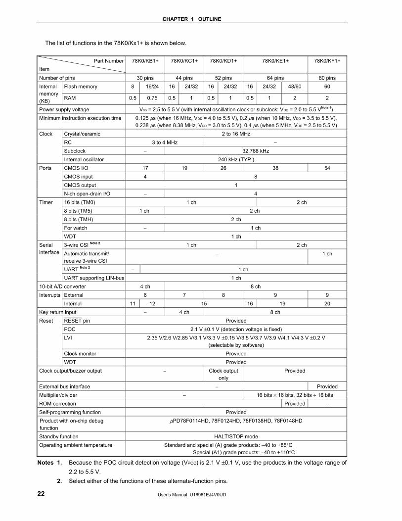
The list of functions in the 78K0/Kx1+ is shown below.
Part Number Item
78K0/KB1+ 78K0/KC1+ 78K0/KD1+ 78K0/KE1+ 78K0/KF1+
Number of pins 30 pins 44 pins 52 pins 64 pins 80 pins Flash memory 8 16/24 16 24/32 16 24/32 16 24/32 48/60 60 Internal
memory (KB) RAM 0.5 0.75 0.5 1 0.5 1 0.5 1 2 2
Power supply voltage VDD = 2.5 to 5.5 V (with internal oscillation clock or subclock: VDD = 2.0 to 5.5 VNote 1) Minimum instruction execution time 0.125 μs (when 16 MHz, VDD = 4.0 to 5.5 V), 0.2 μs (when 10 MHz, VDD = 3.5 to 5.5 V),
0.238 μs (when 8.38 MHz, VDD = 3.0 to 5.5 V), 0.4 μs (when 5 MHz, VDD = 2.5 to 5.5 V) Crystal/ceramic 2 to 16 MHz RC 3 to 4 MHz − Subclock − 32.768 kHz
Clock
Internal oscillator 240 kHz (TYP.) CMOS I/O 17 19 26 38 54 CMOS input 4 8 CMOS output 1
Ports
N-ch open-drain I/O − 4 16 bits (TM0) 1 ch 2 ch 8 bits (TM5) 1 ch 2 ch 8 bits (TMH) 2 ch For watch − 1 ch
Timer
WDT 1 ch 3-wire CSI Note 2 1 ch 2 ch Automatic transmit/ receive 3-wire CSI
− 1 ch
UART Note 2 − 1 ch
Serial interface
UART supporting LIN-bus 1 ch 10-bit A/D converter 4 ch 8 ch
External 6 7 8 9 9 Interrupts Internal 11 12 15 16 19 20
Key return input − 4 ch 8 ch RESET pin Provided POC 2.1 V ±0.1 V (detection voltage is fixed) LVI 2.35 V/2.6 V/2.85 V/3.1 V/3.3 V ±0.15 V/3.5 V/3.7 V/3.9 V/4.1 V/4.3 V ±0.2 V
(selectable by software) Clock monitor Provided
Reset
WDT Provided Clock output/buzzer output − Clock output
only Provided
External bus interface − Provided Multiplier/divider − 16 bits × 16 bits, 32 bits ÷ 16 bits ROM correction − Provided − Self-programming function Provided Product with on-chip debug function
μPD78F0114HD, 78F0124HD, 78F0138HD, 78F0148HD
Standby function HALT/STOP mode Operating ambient temperature Standard and special (A) grade products: −40 to +85°C
Special (A1) grade products: −40 to +110°C
Notes 1. Because the POC circuit detection voltage (VPOC) is 2.1 V ±0.1 V, use the products in the voltage range of 2.2 to 5.5 V.
2. Select either of the functions of these alternate-function pins.
CHAPTER 1 OUTLINE
User’s Manual U16961EJ4V0UD 23
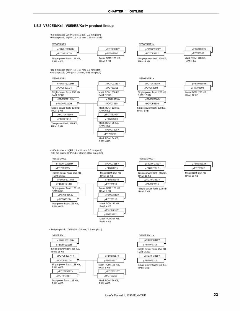
1.5.2 V850ES/Kx1, V850ES/Kx1+ product lineup
V850ES/KE1 V850ES/KE1+
V850ES/KF1 V850ES/KF1+
V850ES/KG1 V850ES/KG1+
V850ES/KJ1 V850ES/KJ1+
• 64-pin plastic LQFP (10 × 10 mm, 0.5 mm pitch) • 64-pin plastic TQFP (12 × 12 mm, 0.65 mm pitch)
• 80-pin plastic TQFP (12 × 12 mm, 0.5 mm pitch) • 80-pin plastic QFP (14 × 14 mm, 0.65 mm pitch)
• 100-pin plastic LQFP (14 × 14 mm, 0.5 mm pitch) • 100-pin plastic QFP (14 × 20 mm, 0.65 mm pitch)
• 144-pin plastic LQFP (20 × 20 mm, 0.5 mm pitch)
Single-power flash: 128 KB,RAM: 4 KB
Mask ROM: 128 KB,RAM: 4 KB
PD70F3207HY
PD70F3207H
PD703207Y
PD703207
PD70F3302Y
PD70F3302
PD703302Y
PD703302
Single-power flash: 128 KB,RAM: 4 KB
Mask ROM: 128 KB,RAM: 4 KB
PD70F3211HY
PD70F3211H
PD703211Y
PD703211
PD70F3308Y
PD70F3308
PD703308Y
PD703308
Single-power flash: 256 KB,RAM: 12 KB
Mask ROM: 256 KB,RAM: 12 KB
Single-power flash: 256 KB,RAM: 12 KB
Mask ROM: 256 KB,RAM: 12 KB
PD703210Y
PD703210
PD70F3210HY
PD70F3210H
PD70F3306Y
PD70F3306
Mask ROM: 128 KB,RAM: 6 KB
Single-power flash: 128 KB,RAM: 6 KB
Single-power flash: 128 KB,RAM: 6 KB
PD703209Y
PD703209
Mask ROM: 96 KB,RAM: 4 KB
PD70F3210Y
PD70F3210
Two-power flash: 128 KB,RAM: 6 KB
PD703208Y
PD703208
Mask ROM: 64 KB,RAM: 4 KB
PD70F3215HY
PD70F3215H
PD703215Y
PD703215
PD70F3313Y
PD70F3313
PD703313Y
PD703313
Single-power flash: 256 KB,RAM: 16 KB
Mask ROM: 256 KB,RAM: 16 KB
Single-power flash: 256 KB,RAM: 16 KB
Mask ROM: 256 KB,RAM: 16 KB
PD703214Y
PD703214
Mask ROM: 128 KB,RAM: 6 KB
PD70F3214HY
PD70F3214H
Single-power flash: 128 KB,RAM: 6 KB
PD70F3311Y
PD70F3311
Single-power flash: 128 KB,RAM: 6 KB
PD703213Y
PD703213
Mask ROM: 96 KB,RAM: 4 KB
PD70F3214Y
PD70F3214
Two-power flash: 128 KB,RAM: 6 KB
PD703212Y
PD703212
Mask ROM: 64 KB,RAM: 4 KB
PD70F3218HY
PD70F3218H
Single-power flash: 256 KB,RAM: 16 KB
PD70F3318Y
PD70F3318
Single-power flash: 256 KB,RAM: 16 KB
PD703217Y
PD703217
Mask ROM: 128 KB,RAM: 6 KB
PD703216Y
PD703216
Mask ROM: 96 KB,RAM: 6 KB
PD70F3217HY
PD70F3217H
Single-power flash: 128 KB,RAM: 6 KB
PD70F3316Y
PD70F3316
Single-power flash: 128 KB,RAM: 6 KB
PD70F3217Y
PD70F3217
Two-power flash: 128 KB,RAM: 6 KB
μ
μ
μ
μ
μ
μ
μ
μ
μ
μ
μ
μ
μ
μ
μ
μ
μ
μ
μ
μ
μ
μ
μ
μ
μ
μ
μ
μ
μ
μ
μ
μ
μ
μ
μ
μ
μ
μ
μ
μ
μ
μ
μ
μ
μ
μ
μ
μ
μ
μ
μ
μ
μ
μ
μ
μ
μ
μ
μ
μ
μ
μ
CHAPTER 1 OUTLINE
User’s Manual U16961EJ4V0UD 24
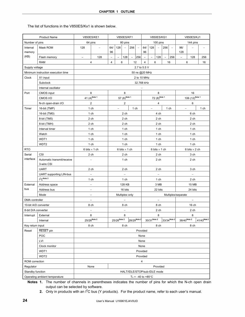
The list of functions in the V850ES/Kx1 is shown below.
Product Name V850ES/KE1 V850ES/KF1 V850ES/KG1 V850ES/KJ1
Number of pins 64 pins 80 pins 100 pins 144 pins
Mask ROM 128 − 64/96
128 − 256 − 64/96
128 − 256 − 96/ 128
− −
Flash memory − 128 − − 128 − 256 − − 128 − 256 − 128 256
Internal memory (KB)
RAM 4 4 6 12 4 6 16 6 16
Supply voltage 2.7 to 5.5 V
Minimum instruction execution time 50 ns @20 MHz
X1 input 2 to 10 MHz
Subclock 32.768 kHz
Clock
Internal oscillator −
CMOS input 8 8 8 16
CMOS I/O 41 (4)Note 1 57 (6)Note 1 72 (8)Note 1 106 (12)Note 1
Port
N-ch open-drain I/O 2 2 4 6
16-bit (TMP) 1 ch − 1 ch − 1 ch − 1 ch
16-bit (TM0) 1 ch 2 ch 4 ch 6 ch
8-bit (TM5) 2 ch 2 ch 2 ch 2 ch
8-bit (TMH) 2 ch 2 ch 2 ch 2 ch
Interval timer 1 ch 1 ch 1 ch 1 ch
Watch 1 ch 1 ch 1 ch 1 ch
WDT1 1 ch 1 ch 1 ch 1 ch
Timer
WDT2 1 ch 1 ch 1 ch 1 ch
RTO 6 bits × 1 ch 6 bits × 1 ch 6 bits × 1 ch 6 bits × 2 ch
CSI 2 ch 2 ch 2 ch 3 ch
Automatic transmit/receive 3-wire CSI
− 1 ch 2 ch 2 ch
UART 2 ch 2 ch 2 ch 3 ch
UART supporting LIN-bus − − − −
Serial interface
I2CNote 2 1 ch 1 ch 1 ch 2 ch
Address space − 128 KB 3 MB 15 MB
Address bus − 16 bits 22 bits 24 bits
External bus
Mode − Multiplex only Multiplex/separate
DMA controller − − − −
10-bit A/D converter 8 ch 8 ch 8 ch 16 ch
8-bit D/A converter − − 2 ch 2 ch
External 8 8 8 8 Interrupt
Internal 25/26Note 2 25/26Note 2 28/29Note 2 30/31Note 2 33/34Note 2 38/40Note 2 41/43Note 2
Key return input 8 ch 8 ch 8 ch 8 ch
RESET pin Provided
POC None
LVI None
Clock monitor None
WDT1 Provided
Reset
WDT2 Provided
ROM correction 4
Regulator None Provided
Standby function HALT/IDLE/STOP/sub-IDLE mode
Operating ambient temperature TA = −40 to +85°C
Notes 1. The number of channels in parentheses indicates the number of pins for which the N-ch open drain output can be selected by software.
2. Only in products with an I2C bus (Y products). For the product name, refer to each user’s manual.
CHAPTER 1 OUTLINE
User’s Manual U16961EJ4V0UD 25
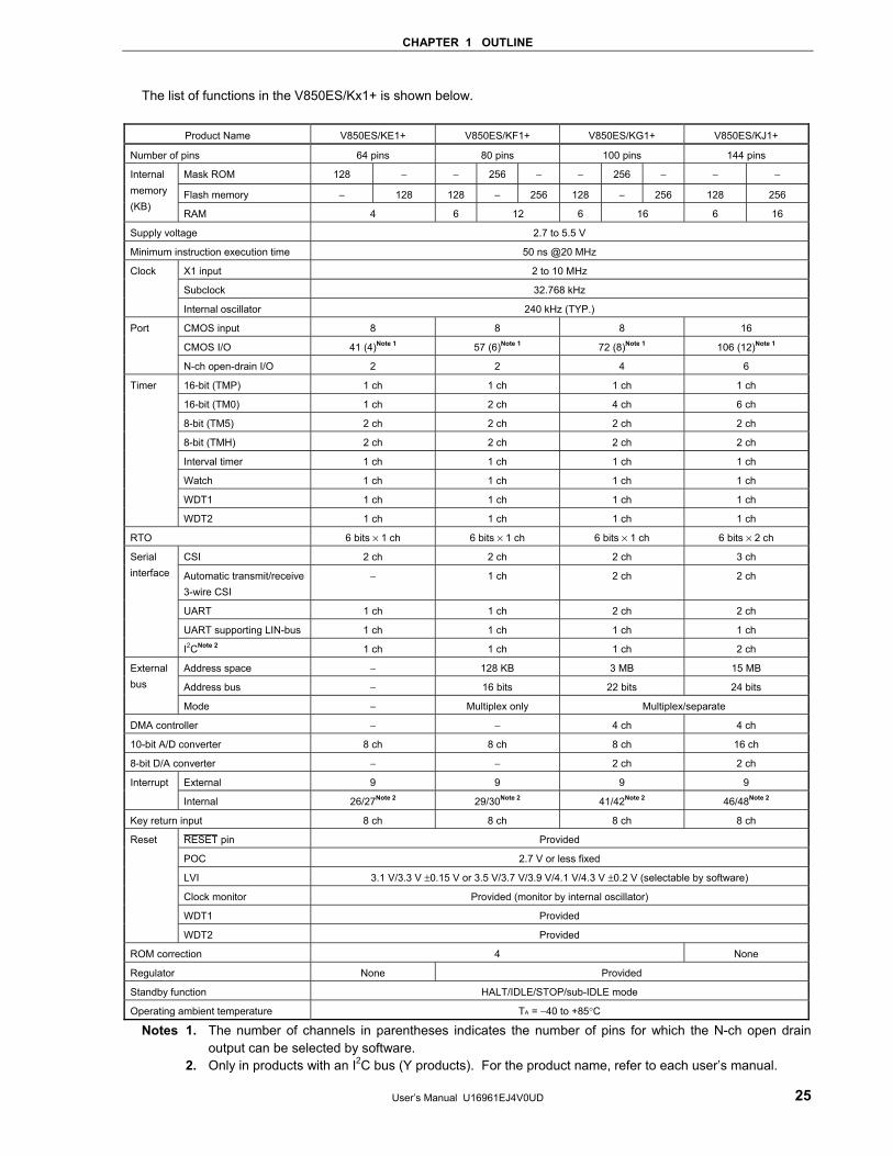
The list of functions in the V850ES/Kx1+ is shown below.
Product Name V850ES/KE1+ V850ES/KF1+ V850ES/KG1+ V850ES/KJ1+
Number of pins 64 pins 80 pins 100 pins 144 pins
Mask ROM 128 − − 256 − − 256 − − −
Flash memory − 128 128 − 256 128 − 256 128 256
Internal memory (KB)
RAM 4 6 12 6 16 6 16
Supply voltage 2.7 to 5.5 V
Minimum instruction execution time 50 ns @20 MHz
X1 input 2 to 10 MHz
Subclock 32.768 kHz
Clock
Internal oscillator 240 kHz (TYP.)
CMOS input 8 8 8 16
CMOS I/O 41 (4)Note 1 57 (6)Note 1 72 (8)Note 1 106 (12)Note 1
Port
N-ch open-drain I/O 2 2 4 6
16-bit (TMP) 1 ch 1 ch 1 ch 1 ch
16-bit (TM0) 1 ch 2 ch 4 ch 6 ch
8-bit (TM5) 2 ch 2 ch 2 ch 2 ch
8-bit (TMH) 2 ch 2 ch 2 ch 2 ch
Interval timer 1 ch 1 ch 1 ch 1 ch
Watch 1 ch 1 ch 1 ch 1 ch
WDT1 1 ch 1 ch 1 ch 1 ch
Timer
WDT2 1 ch 1 ch 1 ch 1 ch
RTO 6 bits × 1 ch 6 bits × 1 ch 6 bits × 1 ch 6 bits × 2 ch
CSI 2 ch 2 ch 2 ch 3 ch
Automatic transmit/receive 3-wire CSI
− 1 ch 2 ch 2 ch
UART 1 ch 1 ch 2 ch 2 ch
UART supporting LIN-bus 1 ch 1 ch 1 ch 1 ch
Serial interface
I2CNote 2 1 ch 1 ch 1 ch 2 ch
Address space − 128 KB 3 MB 15 MB
Address bus − 16 bits 22 bits 24 bits
External bus
Mode − Multiplex only Multiplex/separate
DMA controller − − 4 ch 4 ch
10-bit A/D converter 8 ch 8 ch 8 ch 16 ch
8-bit D/A converter − − 2 ch 2 ch
External 9 9 9 9 Interrupt
Internal 26/27Note 2 29/30Note 2 41/42Note 2 46/48Note 2
Key return input 8 ch 8 ch 8 ch 8 ch
RESET pin Provided
POC 2.7 V or less fixed
LVI 3.1 V/3.3 V ±0.15 V or 3.5 V/3.7 V/3.9 V/4.1 V/4.3 V ±0.2 V (selectable by software)
Clock monitor Provided (monitor by internal oscillator)
WDT1 Provided
Reset
WDT2 Provided
ROM correction 4 None
Regulator None Provided
Standby function HALT/IDLE/STOP/sub-IDLE mode
Operating ambient temperature TA = −40 to +85°C
Notes 1. The number of channels in parentheses indicates the number of pins for which the N-ch open drain output can be selected by software.
2. Only in products with an I2C bus (Y products). For the product name, refer to each user’s manual.
CHAPTER 1 OUTLINE
User’s Manual U16961EJ4V0UD 26
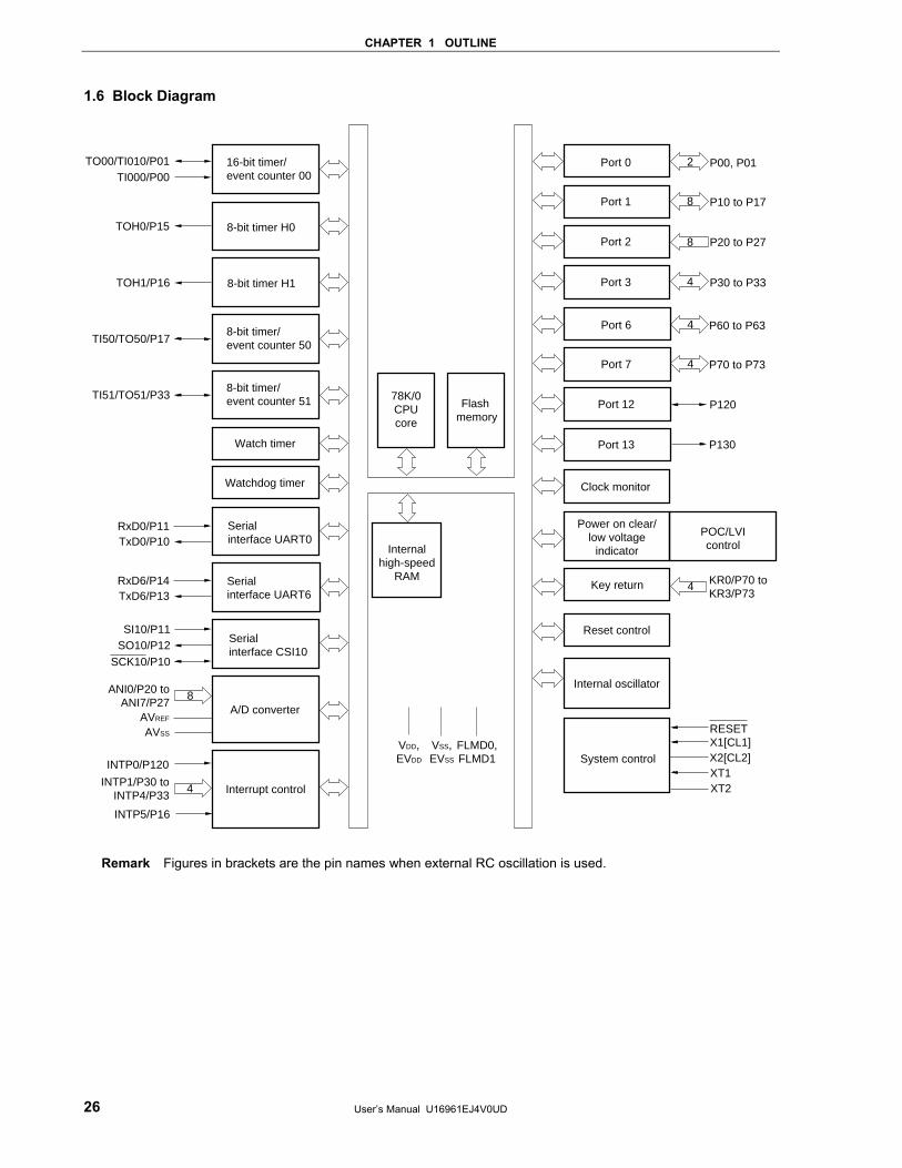
1.6 Block Diagram
16-bit timer/event counter 00
TO00/TI010/P01TI000/P00
Port 0 P00, P012
Port 1 P10 to P17
Port 2 P20 to P278
Port 3 P30 to P334
78K/0CPUcore
Internalhigh-speed
RAM
Flash memory
VSS,EVSS
FLMD0,FLMD1
VDD,EVDD
Serialinterface CSI10
SI10/P11SO10/P12
SCK10/P10
ANI0/P20 toANI7/P27
Interrupt control
8-bit timer H0TOH0/P15
8-bit timer H1TOH1/P16
TI50/TO50/P178-bit timer/event counter 50
8A/D converter
RxD0/P11TxD0/P10
Serialinterface UART0
Watchdog timer
RxD6/P14TxD6/P13
Serialinterface UART6
AVREF
AVSS
INTP1/P30 toINTP4/P33
4
INTP0/P120
8
System control
RESETX1[CL1]X2[CL2]
Clock monitor
Power on clear/low voltage
indicator
POC/LVIcontrol
Reset control
Port 6 P60 to P634
Port 7 P70 to P73
Port 12 P120
Port 13 P130
4
Internal oscillator
XT1XT2
TI51/TO51/P338-bit timer/event counter 51
Watch timer
INTP5/P16
Key return 4 KR0/P70 to KR3/P73
Remark Figures in brackets are the pin names when external RC oscillation is used.
CHAPTER 1 OUTLINE
User’s Manual U16961EJ4V0UD 27
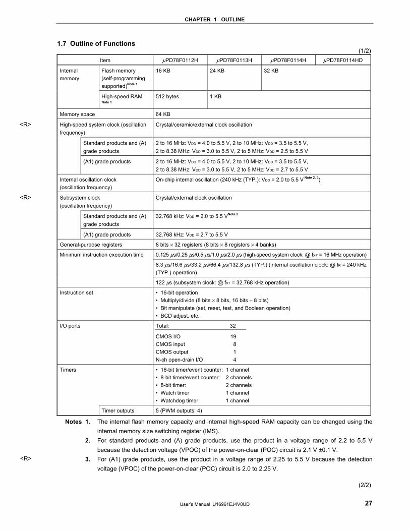
1.7 Outline of Functions (1/2)
Item μPD78F0112H μPD78F0113H μPD78F0114H μPD78F0114HD
Flash memory (self-programming supported)Note 1
16 KB 24 KB 32 KB Internal memory
High-speed RAM Note 1
512 bytes 1 KB
Memory space 64 KB
High-speed system clock (oscillation frequency)
Crystal/ceramic/external clock oscillation
Standard products and (A) grade products
2 to 16 MHz: VDD = 4.0 to 5.5 V, 2 to 10 MHz: VDD = 3.5 to 5.5 V, 2 to 8.38 MHz: VDD = 3.0 to 5.5 V, 2 to 5 MHz: VDD = 2.5 to 5.5 V
(A1) grade products 2 to 16 MHz: VDD = 4.0 to 5.5 V, 2 to 10 MHz: VDD = 3.5 to 5.5 V, 2 to 8.38 MHz: VDD = 3.0 to 5.5 V, 2 to 5 MHz: VDD = 2.7 to 5.5 V
Internal oscillation clock (oscillation frequency)
On-chip internal oscillation (240 kHz (TYP.): VDD = 2.0 to 5.5 V Note 2, 3)
Subsystem clock (oscillation frequency)
Crystal/external clock oscillation
Standard products and (A) grade products
32.768 kHz: VDD = 2.0 to 5.5 VNote 2
(A1) grade products 32.768 kHz: VDD = 2.7 to 5.5 V
General-purpose registers 8 bits × 32 registers (8 bits × 8 registers × 4 banks)
0.125 μs/0.25 μs/0.5 μs/1.0 μs/2.0 μs (high-speed system clock: @ fXP = 16 MHz operation)
8.3 μs/16.6 μs/33.2 μs/66.4 μs/132.8 μs (TYP.) (internal oscillation clock: @ fR = 240 kHz (TYP.) operation)
Minimum instruction execution time
122 μs (subsystem clock: @ fXT = 32.768 kHz operation)
Instruction set • 16-bit operation • Multiply/divide (8 bits × 8 bits, 16 bits ÷ 8 bits) • Bit manipulate (set, reset, test, and Boolean operation) • BCD adjust, etc.
I/O ports Total: 32
CMOS I/O 19 CMOS input 8 CMOS output 1 N-ch open-drain I/O 4
Timers • 16-bit timer/event counter: 1 channel • 8-bit timer/event counter: 2 channels • 8-bit timer: 2 channels • Watch timer 1 channel • Watchdog timer: 1 channel
Timer outputs 5 (PWM outputs: 4)
Notes 1. The internal flash memory capacity and internal high-speed RAM capacity can be changed using the internal memory size switching register (IMS).
2. For standard products and (A) grade products, use the product in a voltage range of 2.2 to 5.5 V because the detection voltage (VPOC) of the power-on-clear (POC) circuit is 2.1 V ±0.1 V.
3. For (A1) grade products, use the product in a voltage range of 2.25 to 5.5 V because the detection voltage (VPOC) of the power-on-clear (POC) circuit is 2.0 to 2.25 V.
(2/2)
<R>
<R>
<R>
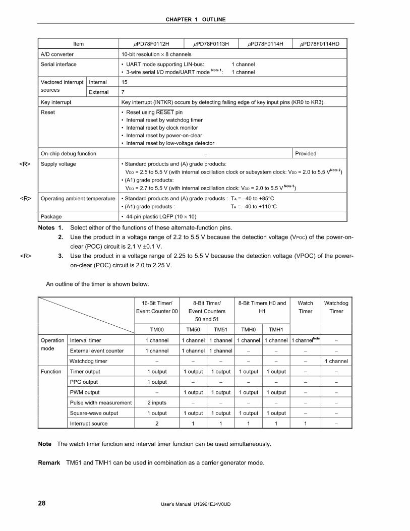
CHAPTER 1 OUTLINE
User’s Manual U16961EJ4V0UD 28
Item μPD78F0112H μPD78F0113H μPD78F0114H μPD78F0114HD
A/D converter 10-bit resolution × 8 channels
Serial interface • UART mode supporting LIN-bus: 1 channel • 3-wire serial I/O mode/UART mode Note 1: 1 channel
Internal 15 Vectored interrupt sources External 7
Key interrupt Key interrupt (INTKR) occurs by detecting falling edge of key input pins (KR0 to KR3).
Reset • Reset using RESET pin • Internal reset by watchdog timer • Internal reset by clock monitor • Internal reset by power-on-clear • Internal reset by low-voltage detector
On-chip debug function − Provided
Supply voltage • Standard products and (A) grade products: VDD = 2.5 to 5.5 V (with internal oscillation clock or subsystem clock: VDD = 2.0 to 5.5 VNote 2)• (A1) grade products: VDD = 2.7 to 5.5 V (with internal oscillation clock: VDD = 2.0 to 5.5 V Note 3)
Operating ambient temperature • Standard products and (A) grade products : TA = −40 to +85°C • (A1) grade products : TA = −40 to +110°C
Package • 44-pin plastic LQFP (10 × 10)
Notes 1. Select either of the functions of these alternate-function pins. 2. Use the product in a voltage range of 2.2 to 5.5 V because the detection voltage (VPOC) of the power-on-
clear (POC) circuit is 2.1 V ±0.1 V. 3. Use the product in a voltage range of 2.25 to 5.5 V because the detection voltage (VPOC) of the power-
on-clear (POC) circuit is 2.0 to 2.25 V.
An outline of the timer is shown below.
16-Bit Timer/ Event Counter 00
8-Bit Timer/ Event Counters
50 and 51
8-Bit Timers H0 and H1
TM00 TM50 TM51 TMH0 TMH1
Watch Timer
Watchdog Timer
Interval timer 1 channel 1 channel 1 channel 1 channel 1 channel 1 channelNote −
External event counter 1 channel 1 channel 1 channel − − − −
Operation mode
Watchdog timer − − − − − − 1 channel
Timer output 1 output 1 output 1 output 1 output 1 output − −
PPG output 1 output − − − − − −
PWM output − 1 output 1 output 1 output 1 output − −
Pulse width measurement 2 inputs − − − − − −
Square-wave output 1 output 1 output 1 output 1 output 1 output − −
Function
Interrupt source 2 1 1 1 1 1 −
Note The watch timer function and interval timer function can be used simultaneously. Remark TM51 and TMH1 can be used in combination as a carrier generator mode.
<R>
<R>
<R>
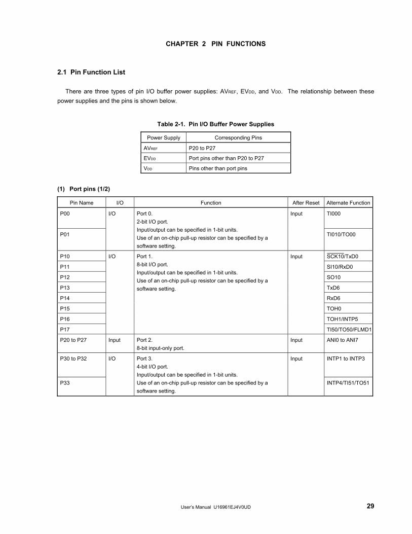
User’s Manual U16961EJ4V0UD 29
CHAPTER 2 PIN FUNCTIONS 2.1 Pin Function List
There are three types of pin I/O buffer power supplies: AVREF, EVDD, and VDD. The relationship between these power supplies and the pins is shown below.
Table 2-1. Pin I/O Buffer Power Supplies
Power Supply Corresponding Pins
AVREF P20 to P27
EVDD Port pins other than P20 to P27
VDD Pins other than port pins
(1) Port pins (1/2)
Pin Name I/O Function After Reset Alternate Function
P00 TI000
P01
I/O Port 0. 2-bit I/O port. Input/output can be specified in 1-bit units. Use of an on-chip pull-up resistor can be specified by a software setting.
Input
TI010/TO00
P10 SCK10/TxD0
P11 SI10/RxD0
P12 SO10
P13 TxD6
P14 RxD6
P15 TOH0
P16 TOH1/INTP5
P17
I/O Port 1. 8-bit I/O port. Input/output can be specified in 1-bit units. Use of an on-chip pull-up resistor can be specified by a software setting.
Input
TI50/TO50/FLMD1
P20 to P27 Input Port 2. 8-bit input-only port.
Input ANI0 to ANI7
P30 to P32 INTP1 to INTP3
P33
I/O Port 3. 4-bit I/O port. Input/output can be specified in 1-bit units. Use of an on-chip pull-up resistor can be specified by a software setting.
Input
INTP4/TI51/TO51
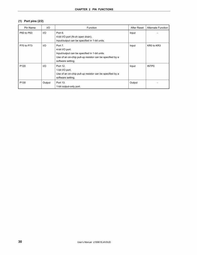
CHAPTER 2 PIN FUNCTIONS
User’s Manual U16961EJ4V0UD 30
(1) Port pins (2/2)
Pin Name I/O Function After Reset Alternate Function
P60 to P63 I/O Port 6. 4-bit I/O port (N-ch open drain). Input/output can be specified in 1-bit units.
Input −
P70 to P73 I/O Port 7. 4-bit I/O port. Input/output can be specified in 1-bit units. Use of an on-chip pull-up resistor can be specified by a software setting.
Input KR0 to KR3
P120 I/O Port 12. 1-bit I/O port. Use of an on-chip pull-up resistor can be specified by a software setting.
Input INTP0
P130 Output Port 13. 1-bit output-only port.
Output −
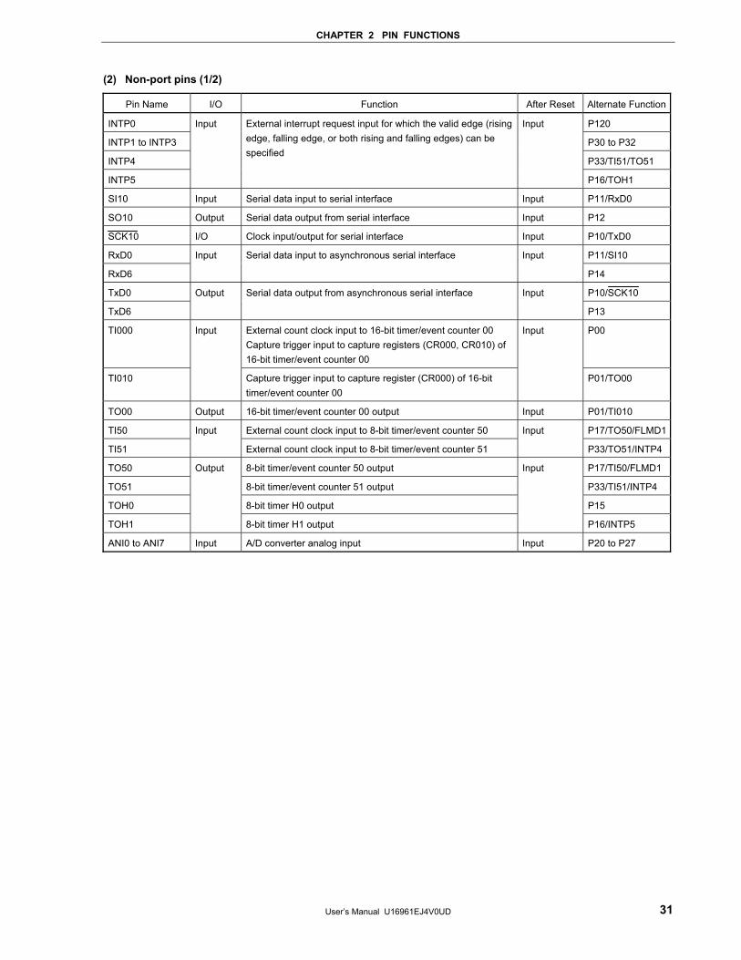
CHAPTER 2 PIN FUNCTIONS
User’s Manual U16961EJ4V0UD 31
(2) Non-port pins (1/2)
Pin Name I/O Function After Reset Alternate Function
INTP0 P120
INTP1 to INTP3 P30 to P32
INTP4 P33/TI51/TO51
INTP5
Input External interrupt request input for which the valid edge (rising edge, falling edge, or both rising and falling edges) can be specified
Input
P16/TOH1
SI10 Input Serial data input to serial interface Input P11/RxD0
SO10 Output Serial data output from serial interface Input P12
SCK10 I/O Clock input/output for serial interface Input P10/TxD0
RxD0 P11/SI10
RxD6
Input Serial data input to asynchronous serial interface Input
P14
TxD0 P10/SCK10
TxD6
Output Serial data output from asynchronous serial interface Input
P13
TI000 External count clock input to 16-bit timer/event counter 00 Capture trigger input to capture registers (CR000, CR010) of 16-bit timer/event counter 00
P00
TI010
Input
Capture trigger input to capture register (CR000) of 16-bit timer/event counter 00
Input
P01/TO00
TO00 Output 16-bit timer/event counter 00 output Input P01/TI010
TI50 External count clock input to 8-bit timer/event counter 50 P17/TO50/FLMD1
TI51
Input
External count clock input to 8-bit timer/event counter 51
Input
P33/TO51/INTP4
TO50 8-bit timer/event counter 50 output P17/TI50/FLMD1
TO51 8-bit timer/event counter 51 output P33/TI51/INTP4
TOH0 8-bit timer H0 output P15
TOH1
Output
8-bit timer H1 output
Input
P16/INTP5
ANI0 to ANI7 Input A/D converter analog input Input P20 to P27
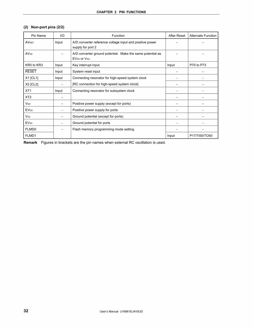
CHAPTER 2 PIN FUNCTIONS
User’s Manual U16961EJ4V0UD 32
(2) Non-port pins (2/2)
Pin Name I/O Function After Reset Alternate Function
AVREF Input A/D converter reference voltage input and positive power supply for port 2
− −
AVSS − A/D converter ground potential. Make the same potential as EVSS or VSS.
− −
KR0 to KR3 Input Key interrupt input Input P70 to P73
RESET Input System reset input − −
X1 [CL1] Input − −
X2 [CL2] −
Connecting resonator for high-speed system clock
[RC connection for high-speed system clock] − −
XT1 Input − −
XT2 −
Connecting resonator for subsystem clock
− −
VDD − Positive power supply (except for ports) − −
EVDD − Positive power supply for ports − −
VSS − Ground potential (except for ports) − −
EVSS − Ground potential for ports − −
FLMD0 − −
FLMD1
− Flash memory programming mode setting.
Input P17/TI50/TO50
Remark Figures in brackets are the pin names when external RC oscillation is used.
CHAPTER 2 PIN FUNCTIONS
User’s Manual U16961EJ4V0UD 33
2.2 Description of Pin Functions 2.2.1 P00 and P01 (port 0)
P00 and P01 function as a 2-bit I/O port. These pins also function as timer I/O. The following operation modes can be specified in 1-bit units.
(1) Port mode
P00 and P01 function as a 2-bit I/O port. P00 and P01 can be set to input or output in 1-bit units using port mode register 0 (PM0). Use of an on-chip pull-up resistor can be specified by pull-up resistor option register 0 (PU0).
(2) Control mode
P00 and P01 function as timer I/O.
(a) TI000 This is the pin for inputting an external count clock to 16-bit timer/event counter 00 and is also for inputting a capture trigger signal to the capture registers (CR000 or CR010) of 16-bit timer/event counter 00.
(b) TI010
This is the pin for inputting a capture trigger signal to the capture register (CR000) of 16-bit timer/event counter 00.
(c) TO00
These are timer output pins.
CHAPTER 2 PIN FUNCTIONS
User’s Manual U16961EJ4V0UD 34
2.2.2 P10 to P17 (port 1) P10 to P17 function as an 8-bit I/O port. These pins also function as pins for external interrupt request input, serial
interface data I/O, clock I/O, timer I/O, and flash memory programming mode setting. The following operation modes can be specified in 1-bit units.
(1) Port mode
P10 to P17 function as an 8-bit I/O port. P10 to P17 can be set to input or output in 1-bit units using port mode register 1 (PM1). Use of an on-chip pull-up resistor can be specified by pull-up resistor option register 1 (PU1).
(2) Control mode
P10 to P17 function as external interrupt request input, serial interface data I/O, clock I/O, timer I/O, and flash memory programming mode setting.
(a) SI10
This is a serial interface serial data input pin.
(b) SO10 This is a serial interface serial data output pin.
(c) SCK10
This is a serial interface serial clock I/O pin.
(d) RxD0, RxD6 These are the serial data input pins of the asynchronous serial interface.
(e) TxD0, TxD6
These are the serial data output pins of the asynchronous serial interface.
(f) TI50 This is the pin for inputting an external count clock to 8-bit timer/event counter 50.
(g) TO50, TOH0, and TOH1
These are timer output pins.
(h) INTP5 This is an external interrupt request input pin for which the valid edge (rising edge, falling edge, or both rising and falling edges) can be specified.
(i) FLMD1
This is the pin for setting the flash memory programming mode.
CHAPTER 2 PIN FUNCTIONS
User’s Manual U16961EJ4V0UD 35
2.2.3 P20 to P27 (port 2) P20 to P27 function as an 8-bit input-only port. These pins also function as pins for A/D converter analog input. The following operation modes can be specified in 1-bit units.
(1) Port mode
P20 to P27 function as an 8-bit input-only port. (2) Control mode
P20 to P27 function as A/D converter analog input pins (ANI0 to ANI7). When using these pins as analog input pins, see (5) ANI0/P20 to ANI7/P27 in 11.6 Cautions for A/D Converter.
2.2.4 P30 to P33 (port 3)
P30 to P33 function as a 4-bit I/O port. These pins also function as pins for external interrupt request input and timer I/O.
The following operation modes can be specified in 1-bit units. (1) Port mode
P30 to P33 function as a 4-bit I/O port. P30 to P33 can be set to input or output in 1-bit units using port mode register 3 (PM3). Use of an on-chip pull-up resistor can be specified by pull-up resistor option register 3 (PU3).
(2) Control mode
P30 to P33 function as external interrupt request input pins and timer I/O pins.
(a) INTP1 to INTP4 These are the external interrupt request input pins for which the valid edge (rising edge, falling edge, or both rising and falling edges) can be specified.
(b) TI51
This is an external count clock input pin to 8-bit timer/event counter 51.
(c) TO51 This is a timer output pin.
Caution In the μPD78F0114HD, be sure to pull the P31 pin down after reset to prevent malfunction.
Remark P31/INTP2 and P32/INTP3 of the μPD78F0138HD can be used as on-chip debug mode setting pins
when the on-chip debug function is used. For details, refer to CHAPTER 24 ON-CHIP DEBUG FUNCTION (μPD78F0114HD ONLY).
2.2.5 P60 to P63 (port 6)
P60 to P63 function as a 4-bit I/O port. P60 to P63 can be set to input port or output port in 1-bit units using port mode register 6 (PM6).
P60 to P63 are N-ch open-drain pins.
CHAPTER 2 PIN FUNCTIONS
User’s Manual U16961EJ4V0UD 36
2.2.6 P70 to P73 (port 7) P70 to P73 function as an 4-bit I/O port. These pins also function as key interrupt input pins. The following operation modes can be specified in 1-bit units.
(1) Port mode
P70 to P73 function as an 4-bit I/O port. P70 to P73 can be set to input or output in 1-bit units using port mode register 7 (PM7). Use of an on-chip pull-up resistor can be specified by pull-up resistor option register 7 (PU7).
(2) Control mode
P70 to P73 function as key interrupt input pins. 2.2.7 P120 (port 12)
P120 functions as a 1-bit I/O port. This pin also functions as a pin for external interrupt request input. The following operation modes can be specified.
(1) Port mode
P120 functions as a 1-bit I/O port. P120 can be set to input or output using port mode register 12 (PM12). Use of an on-chip pull-up resistor can be specified by pull-up resistor option register 12 (PU12).
(2) Control mode
P120 functions as an external interrupt request input pin (INTP0) for which the valid edge (rising edge, falling edge, or both rising and falling edges) can be specified.
2.2.8 P130 (port 13)
P130 functions as a 1-bit output-only port. 2.2.9 AVREF
This is the A/D converter reference voltage input pin. When the A/D converter is not used, connect this pin directly to EVDD or VDD
Note.
Note Connect port 2 directly to EVDD when it is used as a digital port. 2.2.10 AVSS
This is the A/D converter ground potential pin. Even when the A/D converter is not used, always use this pin with the same potential as the EVSS pin or VSS pin. 2.2.11 RESET
This is the active-low system reset input pin. 2.2.12 X1 and X2
These are the pins for connecting a resonator for high-speed system clock. When supplying an external clock, input a signal to the X1 pin and input the inverse signal to the X2 pin.
Remark The X1 and X2 pins of the μPD78F0114HD can be used as on-chip debug mode setting pins when the
on-chip debug function is used. For details, refer to CHAPTER 24 ON-CHIP DEBUG FUNCTION (μPD78F0114HD ONLY).
CHAPTER 2 PIN FUNCTIONS
User’s Manual U16961EJ4V0UD 37
2.2.13 CL1 and CL2 These are the pins for connecting a resistor (R) and capacitor (C) for high-speed system clock oscillation. When supplying an external clock, input a signal to the CL1 pin and input the inverse signal to the CL2 pin.
2.2.14 XT1 and XT2
These are the pins for connecting a resonator for subsystem clock. When supplying an external clock, input a signal to the XT1 pin and input the inverse signal to the XT2 pin.
2.2.15 VDD and EVDD
VDD is the positive power supply pin for other than ports. EVDD is the positive power supply pin for ports.
2.2.16 VSS and EVSS
VSS is the ground potential pin for other than ports. EVSS is the ground potential pin for ports.
2.2.17 FLMD0 and FLMD1
This is a pin for setting flash memory programming mode. Connect FLMD0 to EVSS or VSS in the normal operation mode (FLMD1 is not used in the normal operation mode). In flash memory programming mode, be sure to connect these pins to the flash programmer.

CHAPTER 2 PIN FUNCTIONS
User’s Manual U16961EJ4V0UD 38
2.3 Pin I/O Circuits and Recommended Connection of Unused Pins
Table 2-2 shows the types of pin I/O circuits and the recommended connections of unused pins. Refer to Figure 2-1 for the configuration of the I/O circuit of each type.
Table 2-2. Pin I/O Circuit Types (1/2)
Pin Name I/O Circuit Type I/O Recommended Connection of Unused Pins
P00/TI000
P01/TI010/TO00
P10/SCK10/TxD0
P11/SI10/RxD0
8-A
P12/SO10
P13/TxD6
5-A
P14/RxD6 8-A
P15/TOH0 5-A
P16/TOH1/INTP5
P17/TI50/TO50/FLMD1
8-A
I/O Input: Independently connect to EVDD or EVSS via a resistor. Output: Leave open.
P20/ANI0 to P27/ANI7 9-C Input Connect to AVREF or AVSS.
P30/INTP1
P31/INTP2 (except μPD78F0114HD)
Input: Independently connect to EVDD or EVSS via a resistor. Output: Leave open.
P31/INTP2 (μPD78F0114HD) Connect to EVSS via a resistor.
P32/INTP3
P33/TI51/TO51/INTP4
8-A
Input: Independently connect to EVDD or EVSS via a resistor. Output: Leave open.
P60, P61 13-R
P62, P63 13-W
Input: Connect to EVSS. Output: Leave this pin open at low-level output after clearing the output latch of the port to 0.
P70/KR0 to P73/KR3
P120/INTP0
8-A
I/O
Input: Independently connect to EVDD or EVSS via a resistor. Output: Leave open.
P130 3-C Output Leave open.
Notes 1. Bit 6 (FRC) of the processor clock control register (PCC) must be set to 1 after reset mode is released. 2. Connect port 2 directly to EVDD when it is used as a digital port.
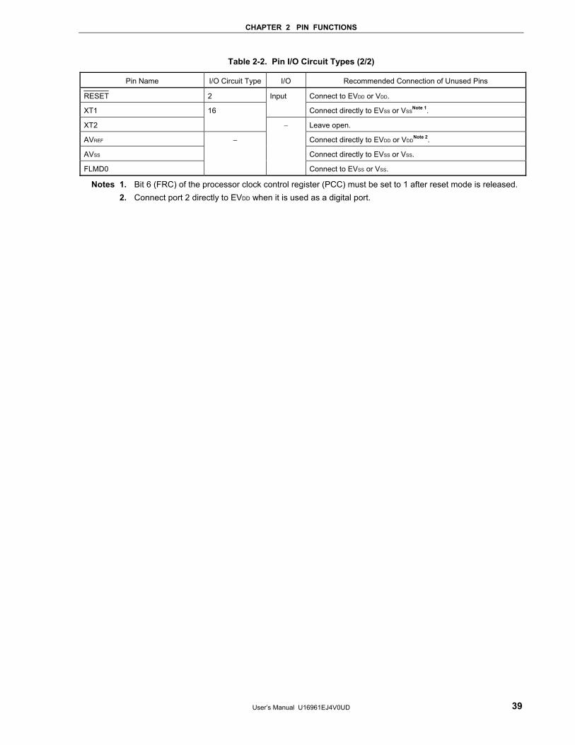
CHAPTER 2 PIN FUNCTIONS
User’s Manual U16961EJ4V0UD 39
Table 2-2. Pin I/O Circuit Types (2/2)
Notes 1. Bit 6 (FRC) of the processor clock control register (PCC) must be set to 1 after reset mode is released. 2. Connect port 2 directly to EVDD when it is used as a digital port.
Pin Name I/O Circuit Type I/O Recommended Connection of Unused Pins
RESET 2 Connect to EVDD or VDD.
XT1
Input
Connect directly to EVSS or VSSNote 1.
XT2
16
Leave open.
AVREF Connect directly to EVDD or VDDNote 2.
AVSS Connect directly to EVSS or VSS.
FLMD0
−
−
Connect to EVSS or VSS.
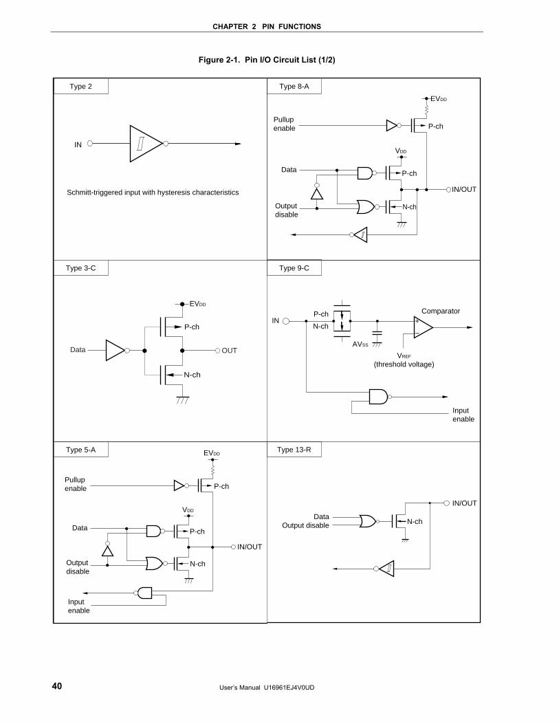
CHAPTER 2 PIN FUNCTIONS
User’s Manual U16961EJ4V0UD 40
Figure 2-1. Pin I/O Circuit List (1/2)
Type 3-C
Type 2 Type 8-A
Type 5-A
Type 9-C
Schmitt-triggered input with hysteresis characteristics
IN
Pullupenable
Data
Outputdisable
EVDD
P-ch
VDD
P-ch
IN/OUT
N-ch
EVDD
P-ch
N-ch
Data OUT
INComparator
VREF
(threshold voltage)
AVSS
P-ch
N-ch
Inputenable
+
–
Pullupenable
Data
Outputdisable
Inputenable
EVDD
P-ch
VDD
P-ch
IN/OUT
N-ch
DataOutput disable
IN/OUT
N-ch
Type 13-R
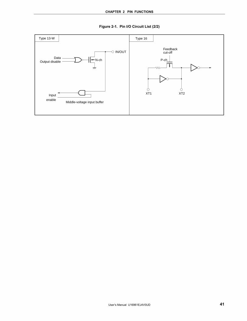
CHAPTER 2 PIN FUNCTIONS
User’s Manual U16961EJ4V0UD 41
Figure 2-1. Pin I/O Circuit List (2/2)
Type 13-W Type 16
DataOutput disable
IN/OUT
N-ch
Inputenable
Middle-voltage input buffer
P-ch
Feedbackcut-off
XT1 XT2
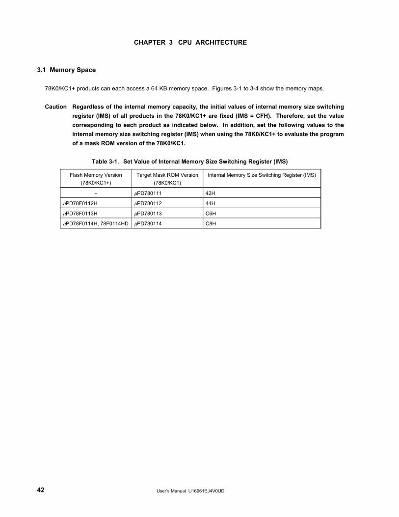
User’s Manual U16961EJ4V0UD 42
CHAPTER 3 CPU ARCHITECTURE 3.1 Memory Space
78K0/KC1+ products can each access a 64 KB memory space. Figures 3-1 to 3-4 show the memory maps.
Caution Regardless of the internal memory capacity, the initial values of internal memory size switching register (IMS) of all products in the 78K0/KC1+ are fixed (IMS = CFH). Therefore, set the value corresponding to each product as indicated below. In addition, set the following values to the internal memory size switching register (IMS) when using the 78K0/KC1+ to evaluate the program of a mask ROM version of the 78K0/KC1.
Table 3-1. Set Value of Internal Memory Size Switching Register (IMS)
Flash Memory Version (78K0/KC1+)
Target Mask ROM Version (78K0/KC1)
Internal Memory Size Switching Register (IMS)
− μPD780111 42H
μPD78F0112H μPD780112 44H
μPD78F0113H μPD780113 C6H
μPD78F0114H, 78F0114HD μPD780114 C8H

CHAPTER 3 CPU ARCHITECTURE
User’s Manual U16961EJ4V0UD 43
Figure 3-1. Memory Map (μPD78F0112H)
0000H
Data memory space
General-purpose registers32 × 8 bits
Flash memory16384 × 8 bits
Programmemoryspace
4000H3FFFH
FEE0HFEDFH
FF00HFEFFH
FFFFH
Internal high-speed RAM512 × 8 bits
Special function registers (SFRs)
256 × 8 bits
Reserved
FD00HFCFFH
0800H07FFH
1000H0FFFH
0040H003FH
0000H
0085H0084H
Program area
3FFFH
Program area
0080H007FH
1085H1084H
1080H107FH
Vector table area64 × 8 bits
CALLT table area64 × 8 bits
Program area1915 × 8 bits
Option byte areaNote
5 × 8 bits
CALLF entry area2048 × 8 bits
Option byte areaNote
5 × 8 bits
1FFFH
Boot cluster 0
Boot cluster 1
Note When boot swap is not used: Set the option bytes to 0080H to 0084H. When boot swap is used: Set the option bytes to 0080H to 0084H and 1080H to 1084H. Caution When replacing the μPD78F0112H with the μPD78F0114HD, note that the area from 0081H to
0083H in the μPD78F0114HD cannot be used.
<R>
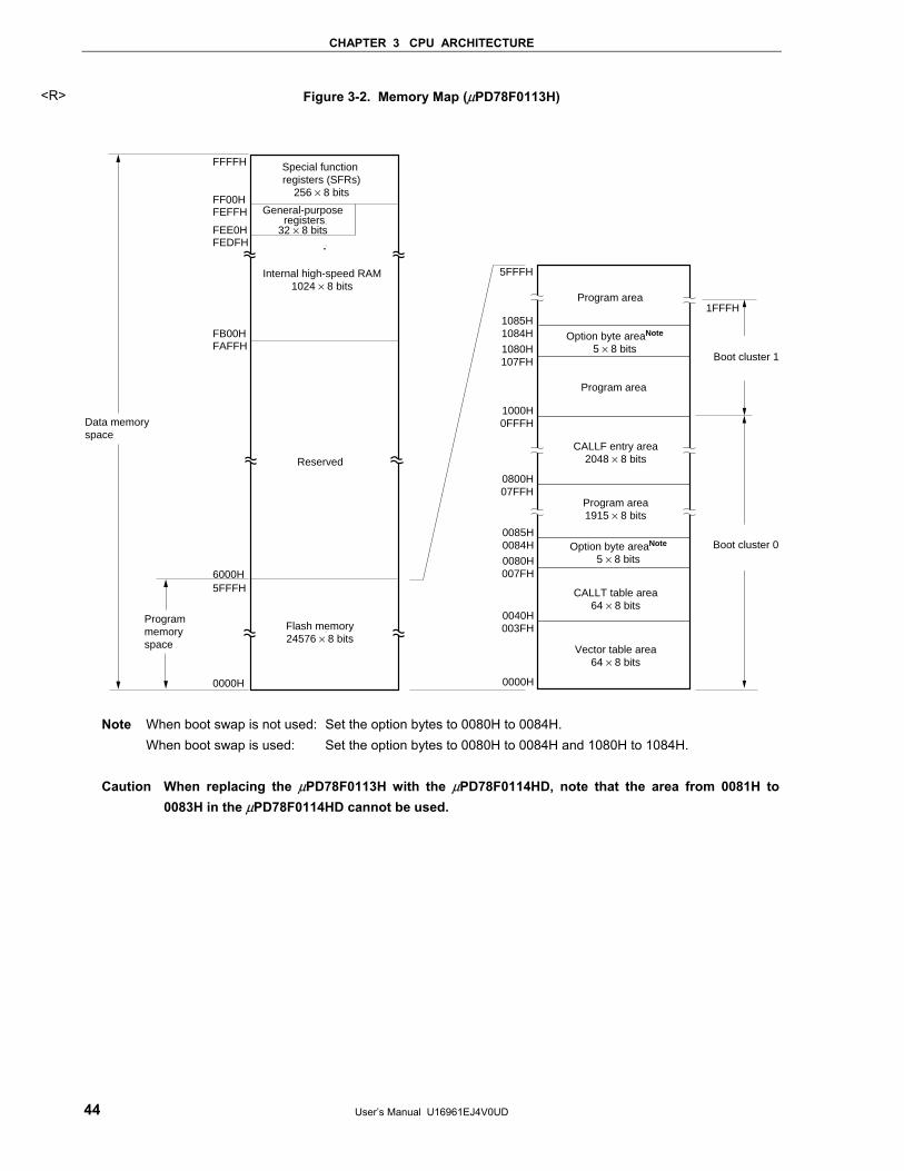
CHAPTER 3 CPU ARCHITECTURE
User’s Manual U16961EJ4V0UD 44
Figure 3-2. Memory Map (μPD78F0113H)
0000H
Data memory space
General-purpose registers32 × 8 bits
Flash memory24576 × 8 bits
Programmemoryspace
6000H5FFFH
FEE0HFEDFH
FF00HFEFFH
FFFFH
Internal high-speed RAM1024 × 8 bits
Special function registers (SFRs)
256 × 8 bits
Reserved
FB00HFAFFH
0800H07FFH
1000H0FFFH
0040H003FH
0000H
0085H0084H
Program area
5FFFH
Program area
0080H007FH
1085H1084H
1080H107FH
Vector table area64 × 8 bits
CALLT table area64 × 8 bits
Program area1915 × 8 bits
Option byte areaNote
5 × 8 bits
CALLF entry area2048 × 8 bits
Option byte areaNote
5 × 8 bits
1FFFH
Boot cluster 0
Boot cluster 1
Note When boot swap is not used: Set the option bytes to 0080H to 0084H. When boot swap is used: Set the option bytes to 0080H to 0084H and 1080H to 1084H. Caution When replacing the μPD78F0113H with the μPD78F0114HD, note that the area from 0081H to
0083H in the μPD78F0114HD cannot be used.
<R>
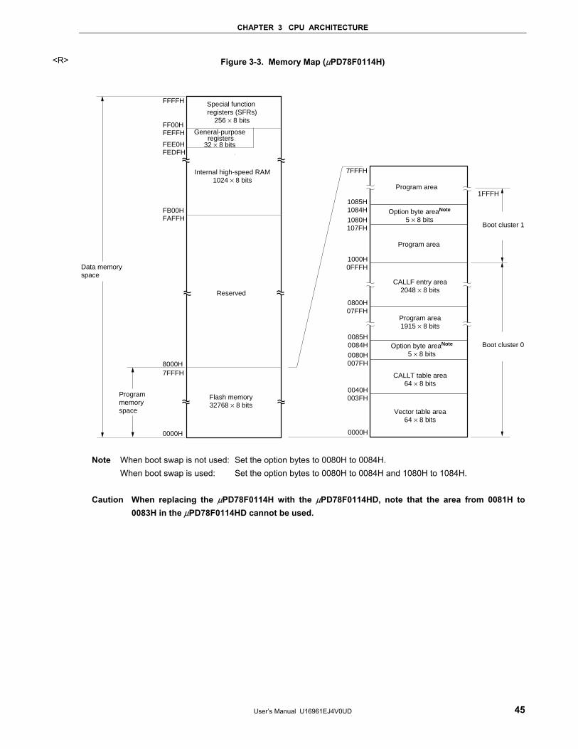
CHAPTER 3 CPU ARCHITECTURE
User’s Manual U16961EJ4V0UD 45
Figure 3-3. Memory Map (μPD78F0114H)
0000H
Data memory space
Flash memory32768 × 8 bits
Programmemoryspace
8000H7FFFH
FEE0HFEDFH
FF00HFEFFH
FFFFH
Internal high-speed RAM1024 × 8 bits
Special function registers (SFRs)
256 × 8 bits
Reserved
FB00HFAFFH
General-purpose registers32 × 8 bits
0800H07FFH
1000H0FFFH
0040H003FH
0000H
0085H0084H
Program area
7FFFH
Program area
0080H007FH
1085H1084H
1080H107FH
Vector table area64 × 8 bits
CALLT table area64 × 8 bits
Program area1915 × 8 bits
Option byte areaNote
5 × 8 bits
CALLF entry area2048 × 8 bits
Option byte areaNote
5 × 8 bits
1FFFH
Boot cluster 0
Boot cluster 1
Note When boot swap is not used: Set the option bytes to 0080H to 0084H. When boot swap is used: Set the option bytes to 0080H to 0084H and 1080H to 1084H. Caution When replacing the μPD78F0114H with the μPD78F0114HD, note that the area from 0081H to
0083H in the μPD78F0114HD cannot be used.
<R>
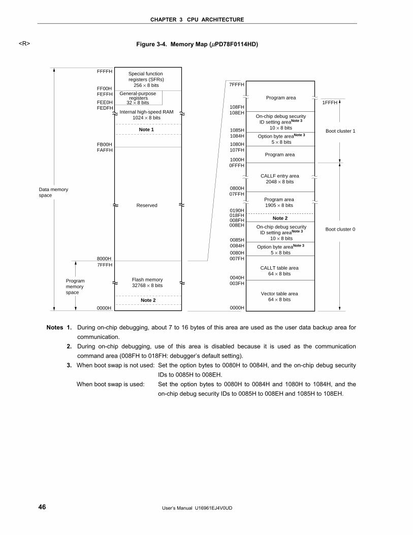
CHAPTER 3 CPU ARCHITECTURE
User’s Manual U16961EJ4V0UD 46
Figure 3-4. Memory Map (μPD78F0114HD)
0000H
Data memory space
General-purpose registers32 × 8 bits
Flash memory32768 × 8 bits
Programmemoryspace
8000H7FFFH
FEE0HFEDFH
FF00HFEFFH
FFFFH
Internal high-speed RAM1024 × 8 bits
Special function registers (SFRs)
256 × 8 bits
Reserved
FB00HFAFFH
Note 1
Note 2
0800H07FFH
1000H0FFFH
0040H003FH
0000H
0085H0084H
Program area1905 × 8 bits
Program area
7FFFH
Program area
0080H007FH
1080H107FH
008FH008EH
1085H1084H
108FH108EH
Vector table area64 × 8 bits
CALLT table area64 × 8 bits
Option byte areaNote 3
5 × 8 bits
On-chip debug securityID setting areaNote 3
10 × 8 bits
Option byte areaNote 3
5 × 8 bits
CALLF entry area2048 × 8 bits
1FFFH
Boot cluster 0
Boot cluster 1
On-chip debug securityID setting areaNote 3
10 × 8 bits
Note 2
0190H018FH
Notes 1. During on-chip debugging, about 7 to 16 bytes of this area are used as the user data backup area for communication.
2. During on-chip debugging, use of this area is disabled because it is used as the communication command area (008FH to 018FH: debugger’s default setting).
3. When boot swap is not used: Set the option bytes to 0080H to 0084H, and the on-chip debug security IDs to 0085H to 008EH.
When boot swap is used: Set the option bytes to 0080H to 0084H and 1080H to 1084H, and the on-chip debug security IDs to 0085H to 008EH and 1085H to 108EH.
<R>
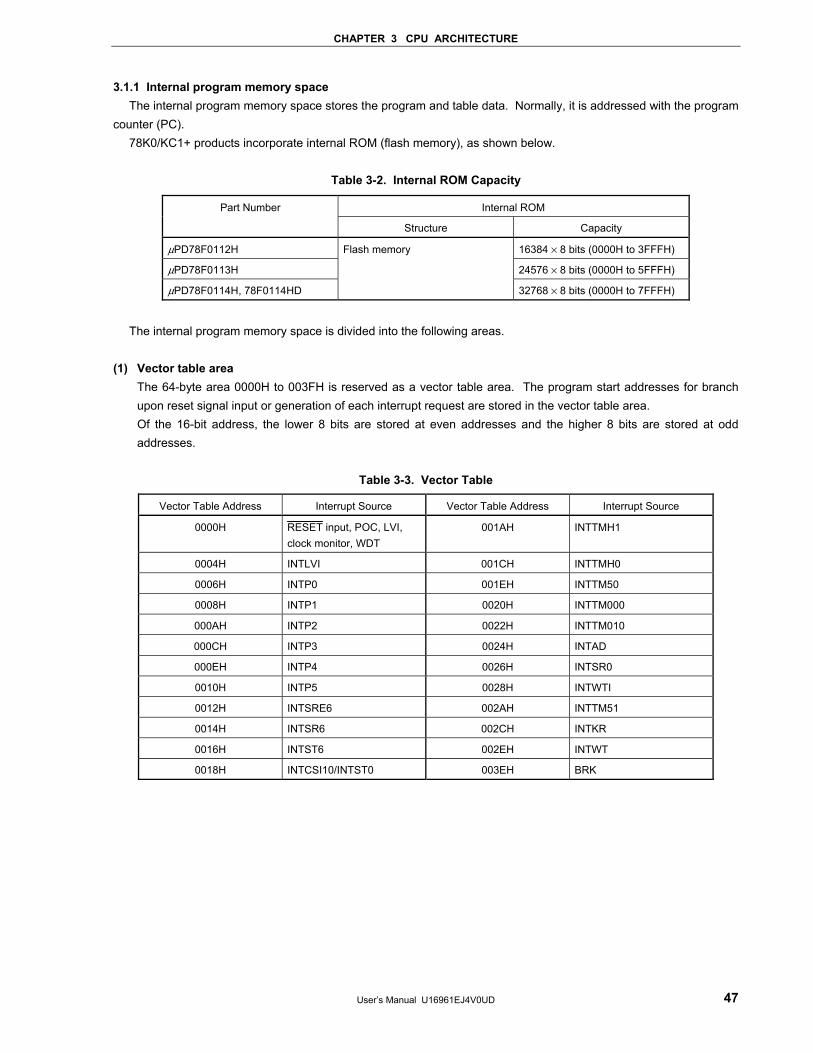
CHAPTER 3 CPU ARCHITECTURE
User’s Manual U16961EJ4V0UD 47
3.1.1 Internal program memory space The internal program memory space stores the program and table data. Normally, it is addressed with the program
counter (PC). 78K0/KC1+ products incorporate internal ROM (flash memory), as shown below.
Table 3-2. Internal ROM Capacity
Internal ROM Part Number
Structure Capacity
μPD78F0112H 16384 × 8 bits (0000H to 3FFFH)
μPD78F0113H 24576 × 8 bits (0000H to 5FFFH)
μPD78F0114H, 78F0114HD
Flash memory
32768 × 8 bits (0000H to 7FFFH)
The internal program memory space is divided into the following areas.
(1) Vector table area
The 64-byte area 0000H to 003FH is reserved as a vector table area. The program start addresses for branch upon reset signal input or generation of each interrupt request are stored in the vector table area. Of the 16-bit address, the lower 8 bits are stored at even addresses and the higher 8 bits are stored at odd addresses.
Table 3-3. Vector Table
Vector Table Address Interrupt Source Vector Table Address Interrupt Source
0000H RESET input, POC, LVI, clock monitor, WDT
001AH INTTMH1
0004H INTLVI 001CH INTTMH0
0006H INTP0 001EH INTTM50
0008H INTP1 0020H INTTM000
000AH INTP2 0022H INTTM010
000CH INTP3 0024H INTAD
000EH INTP4 0026H INTSR0
0010H INTP5 0028H INTWTI
0012H INTSRE6 002AH INTTM51
0014H INTSR6 002CH INTKR
0016H INTST6 002EH INTWT
0018H INTCSI10/INTST0 003EH BRK
CHAPTER 3 CPU ARCHITECTURE
User’s Manual U16961EJ4V0UD 48
(2) CALLT instruction table area The 64-byte area 0040H to 007FH can store the subroutine entry address of a 1-byte call instruction (CALLT).
(3) Option byte area
The option byte area is assigned to the 1-byte area of 0080H. Refer to CHAPTER 22 OPTION BYTE for details. (4) CALLF instruction entry area
The area 0800H to 0FFFH can perform a direct subroutine call with a 2-byte call instruction (CALLF). 3.1.2 Internal data memory space
78K0/KC1+ products incorporate the following internal high-speed RAMs.
Table 3-4. Internal High-Speed RAM Capacity
Part Number Internal Expansion RAM
μPD78F0112H 512 × 8 bits (FD00H to FEFFH)
μPD78F0113H
μPD78F0114H, 78F0114HD
1024 × 8 bits (FB00H to FEFFH)
The 32-byte area FEE0H to FEFFH is assigned to four general-purpose register banks consisting of eight 8-bit
registers per one bank. This area cannot be used as a program area in which instructions are written and executed. The internal high-speed RAM can also be used as a stack memory.
3.1.3 Special function register (SFR) area
On-chip peripheral hardware special function registers (SFRs) are allocated in the area FF00H to FFFFH (refer to Table 3-5 Special Function Register List in 3.2.3 Special function registers (SFRs)).
Caution Do not access addresses to which SFRs are not assigned.
CHAPTER 3 CPU ARCHITECTURE
User’s Manual U16961EJ4V0UD 49
3.1.4 Data memory addressing Addressing refers to the method of specifying the address of the instruction to be executed next or the address of
the register or memory relevant to the execution of instructions. Several addressing modes are provided for addressing the memory relevant to the execution of instructions for the
78K0/KC1+, based on operability and other considerations. For areas containing data memory in particular, special addressing methods designed for the functions of special function registers (SFR) and general-purpose registers are available for use. Figures 3-5 to 3-8 show correspondence between data memory and addressing. For the details of each addressing mode, see 3.4 Operand Address Addressing.
Figure 3-5. Correspondence Between Data Memory and Addressing (μPD78F0112H)
0000H
General-purpose registers32 × 8 bits
Flash memory16384 × 8 bits
4000H3FFFH
FEE0HFEDFH
FF00HFEFFH
FFFFH
Internal high-speed RAM512 × 8 bits
Reserved
FD00HFCFFH
FF20HFF1FH
FE20HFE1FH
Special function registers (SFRs)
256 × 8 bitsSFR addressing
Register addressingShort direct addressing
Direct addressing
Register indirectaddressing
Based addressing
Based indexedaddressing
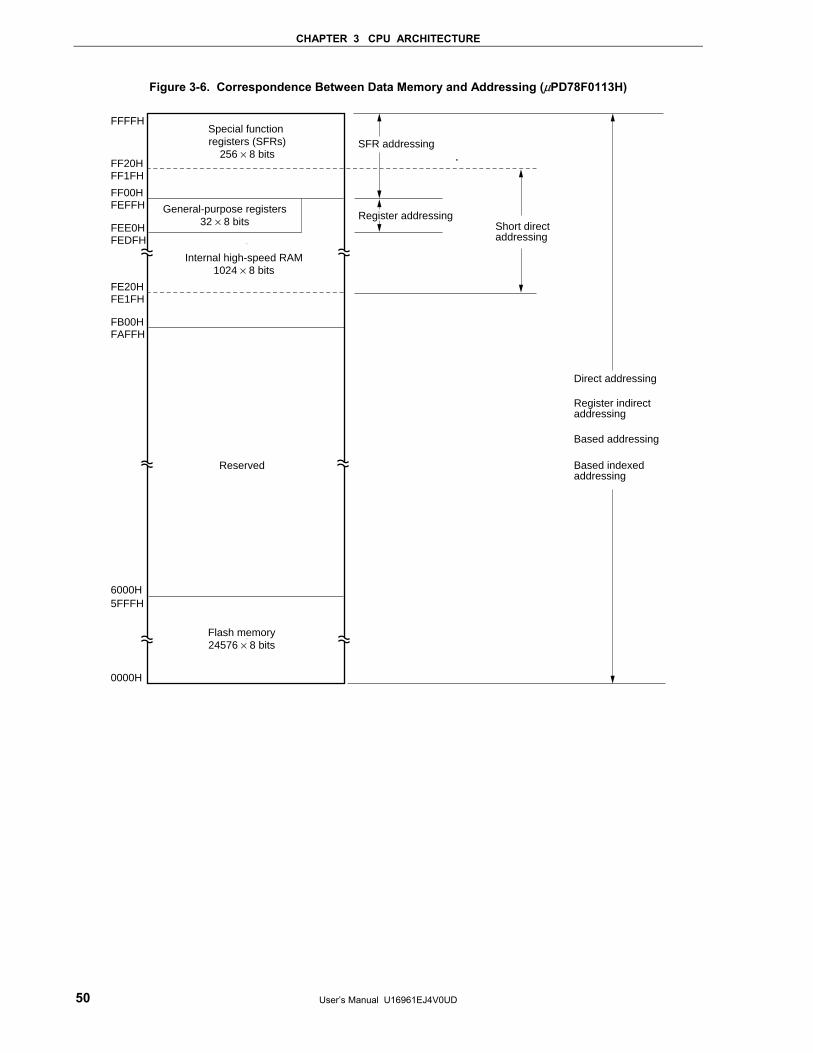
CHAPTER 3 CPU ARCHITECTURE
User’s Manual U16961EJ4V0UD 50
Figure 3-6. Correspondence Between Data Memory and Addressing (μPD78F0113H)
0000H
General-purpose registers32 × 8 bits
Flash memory24576 × 8 bits
6000H5FFFH
FEE0HFEDFH
FF00HFEFFH
FFFFH
Internal high-speed RAM1024 × 8 bits
Reserved
FB00HFAFFH
FF20HFF1FH
FE20HFE1FH
Special function registers (SFRs)
256 × 8 bitsSFR addressing
Register addressingShort direct addressing
Direct addressing
Register indirectaddressing
Based addressing
Based indexedaddressing
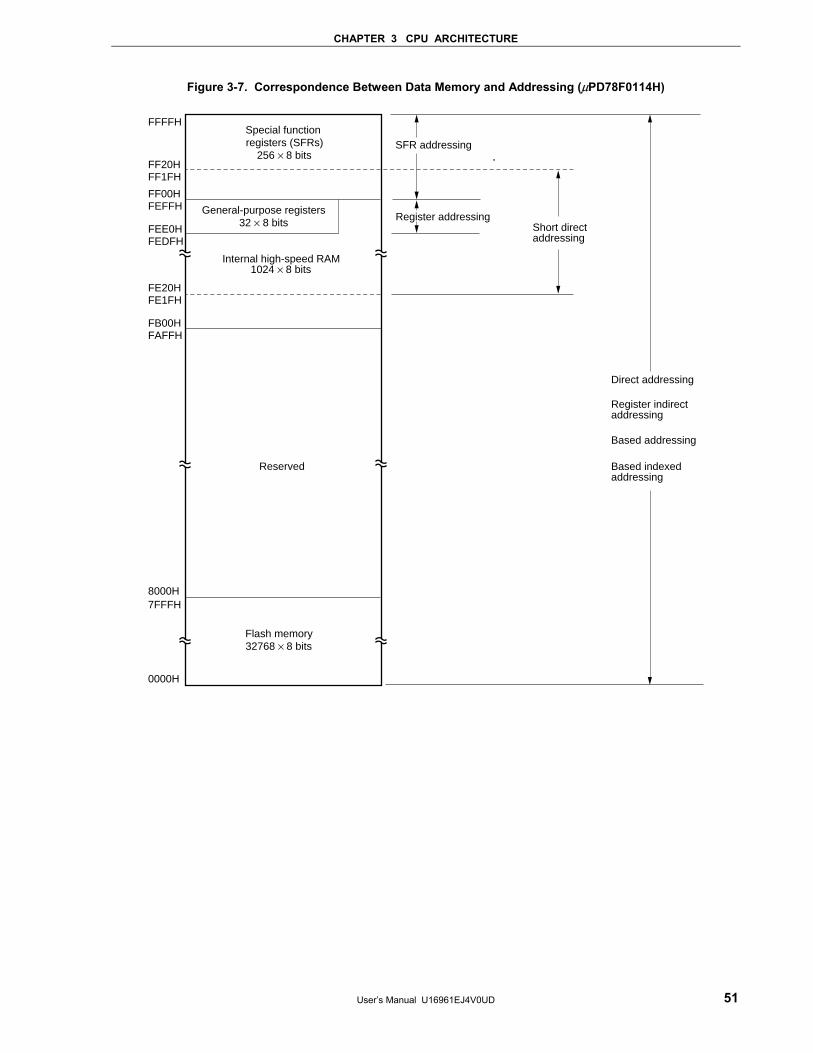
CHAPTER 3 CPU ARCHITECTURE
User’s Manual U16961EJ4V0UD 51
Figure 3-7. Correspondence Between Data Memory and Addressing (μPD78F0114H)
0000H
General-purpose registers32 × 8 bits
Flash memory32768 × 8 bits
8000H7FFFH
FEE0HFEDFH
FF00HFEFFH
FFFFH
Internal high-speed RAM1024 × 8 bits
Reserved
FB00HFAFFH
FF20HFF1FH
FE20HFE1FH
Special function registers (SFRs)
256 × 8 bitsSFR addressing
Register addressingShort direct addressing
Direct addressing
Register indirectaddressing
Based addressing
Based indexedaddressing
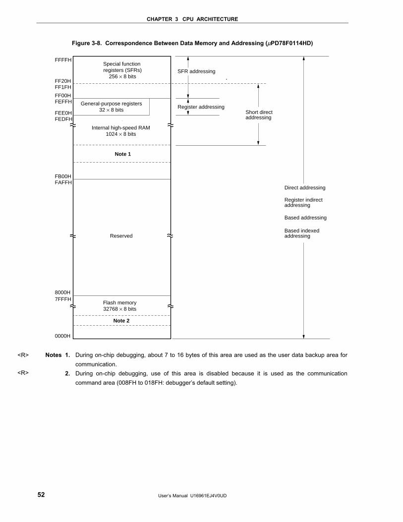
CHAPTER 3 CPU ARCHITECTURE
User’s Manual U16961EJ4V0UD 52
Figure 3-8. Correspondence Between Data Memory and Addressing (μPD78F0114HD)
0000H
General-purpose registers32 × 8 bits
Flash memory32768 × 8 bits
8000H7FFFH
FEE0HFEDFH
FF00HFEFFH
FFFFH
Internal high-speed RAM1024 × 8 bits
Reserved
FF20HFF1FH
Special function registers (SFRs)
256 × 8 bitsSFR addressing
Register addressingShort direct addressing
Direct addressing
Register indirectaddressing
Based addressing
Based indexedaddressing
FB00HFAFFH
Note 1
Note 2
Notes 1. During on-chip debugging, about 7 to 16 bytes of this area are used as the user data backup area for communication.
2. During on-chip debugging, use of this area is disabled because it is used as the communication command area (008FH to 018FH: debugger’s default setting).
<R>
<R>
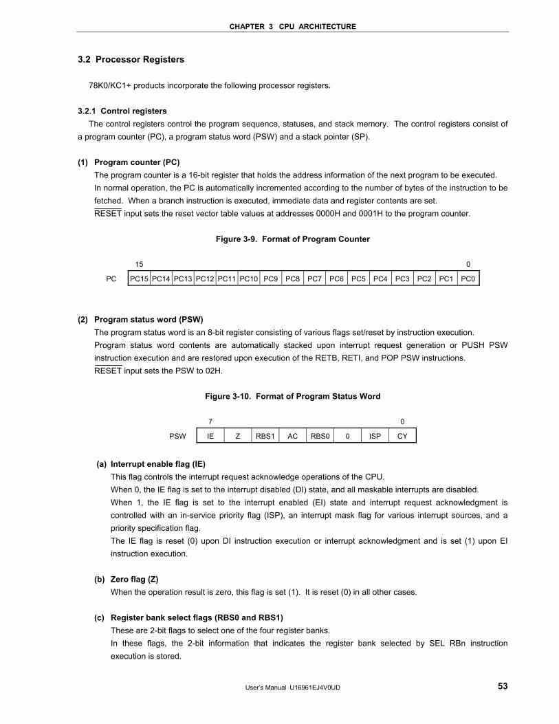
CHAPTER 3 CPU ARCHITECTURE
User’s Manual U16961EJ4V0UD 53
3.2 Processor Registers
78K0/KC1+ products incorporate the following processor registers. 3.2.1 Control registers
The control registers control the program sequence, statuses, and stack memory. The control registers consist of a program counter (PC), a program status word (PSW) and a stack pointer (SP). (1) Program counter (PC)
The program counter is a 16-bit register that holds the address information of the next program to be executed. In normal operation, the PC is automatically incremented according to the number of bytes of the instruction to be fetched. When a branch instruction is executed, immediate data and register contents are set. RESET input sets the reset vector table values at addresses 0000H and 0001H to the program counter.
Figure 3-9. Format of Program Counter
15 0
PC PC15 PC14 PC13 PC12 PC11 PC10 PC9 PC8 PC7 PC6 PC5 PC4 PC3 PC2 PC1 PC0
(2) Program status word (PSW)
The program status word is an 8-bit register consisting of various flags set/reset by instruction execution. Program status word contents are automatically stacked upon interrupt request generation or PUSH PSW instruction execution and are restored upon execution of the RETB, RETI, and POP PSW instructions. RESET input sets the PSW to 02H.
Figure 3-10. Format of Program Status Word
7 0
PSW IE Z RBS1 AC RBS0 0 ISP CY
(a) Interrupt enable flag (IE)
This flag controls the interrupt request acknowledge operations of the CPU. When 0, the IE flag is set to the interrupt disabled (DI) state, and all maskable interrupts are disabled. When 1, the IE flag is set to the interrupt enabled (EI) state and interrupt request acknowledgment is controlled with an in-service priority flag (ISP), an interrupt mask flag for various interrupt sources, and a priority specification flag. The IE flag is reset (0) upon DI instruction execution or interrupt acknowledgment and is set (1) upon EI instruction execution.
(b) Zero flag (Z)
When the operation result is zero, this flag is set (1). It is reset (0) in all other cases.
(c) Register bank select flags (RBS0 and RBS1) These are 2-bit flags to select one of the four register banks. In these flags, the 2-bit information that indicates the register bank selected by SEL RBn instruction execution is stored.
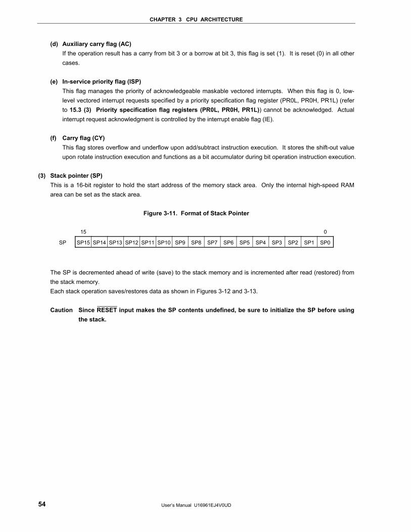
CHAPTER 3 CPU ARCHITECTURE
User’s Manual U16961EJ4V0UD 54
(d) Auxiliary carry flag (AC) If the operation result has a carry from bit 3 or a borrow at bit 3, this flag is set (1). It is reset (0) in all other cases.
(e) In-service priority flag (ISP)
This flag manages the priority of acknowledgeable maskable vectored interrupts. When this flag is 0, low-level vectored interrupt requests specified by a priority specification flag register (PR0L, PR0H, PR1L) (refer to 15.3 (3) Priority specification flag registers (PR0L, PR0H, PR1L)) cannot be acknowledged. Actual interrupt request acknowledgment is controlled by the interrupt enable flag (IE).
(f) Carry flag (CY)
This flag stores overflow and underflow upon add/subtract instruction execution. It stores the shift-out value upon rotate instruction execution and functions as a bit accumulator during bit operation instruction execution.
(3) Stack pointer (SP)
This is a 16-bit register to hold the start address of the memory stack area. Only the internal high-speed RAM area can be set as the stack area.
Figure 3-11. Format of Stack Pointer
15 0
SP SP15 SP14 SP13 SP12 SP11 SP10 SP9 SP8 SP7 SP6 SP5 SP4 SP3 SP2 SP1 SP0
The SP is decremented ahead of write (save) to the stack memory and is incremented after read (restored) from the stack memory. Each stack operation saves/restores data as shown in Figures 3-12 and 3-13.
Caution Since RESET input makes the SP contents undefined, be sure to initialize the SP before using
the stack.
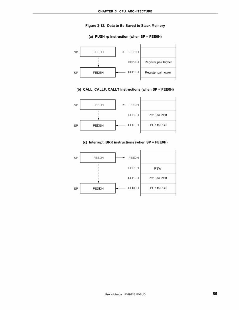
CHAPTER 3 CPU ARCHITECTURE
User’s Manual U16961EJ4V0UD 55
Figure 3-12. Data to Be Saved to Stack Memory
(a) PUSH rp instruction (when SP = FEE0H)
Register pair lower
FEE0HSP
SP
FEE0H
FEDFH
FEDEH
Register pair higher
FEDEH
(b) CALL, CALLF, CALLT instructions (when SP = FEE0H)
PC15 to PC8
FEE0HSP
SP
FEE0H
FEDFH
FEDEH PC7 to PC0FEDEH
(c) Interrupt, BRK instructions (when SP = FEE0H)
PC15 to PC8
PSWFEDFH
FEE0HSP
SP
FEE0H
FEDEH
FEDDH PC7 to PC0FEDDH
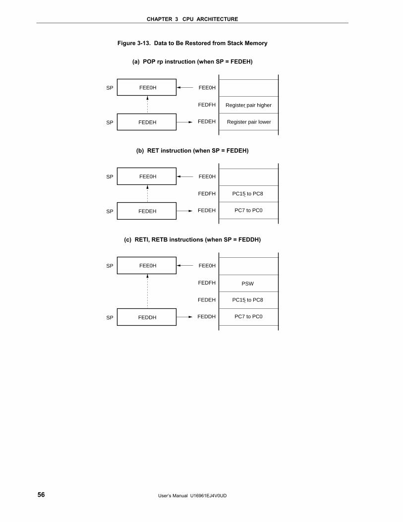
CHAPTER 3 CPU ARCHITECTURE
User’s Manual U16961EJ4V0UD 56
Figure 3-13. Data to Be Restored from Stack Memory
(a) POP rp instruction (when SP = FEDEH)
Register pair lower
FEE0HSP
SP
FEE0H
FEDFH
FEDEH
Register pair higher
FEDEH
(b) RET instruction (when SP = FEDEH)
PC15 to PC8
FEE0HSP
SP
FEE0H
FEDFH
FEDEH PC7 to PC0FEDEH
(c) RETI, RETB instructions (when SP = FEDDH)
PC15 to PC8
PSWFEDFH
FEE0HSP
SP
FEE0H
FEDEH
FEDDH PC7 to PC0FEDDH
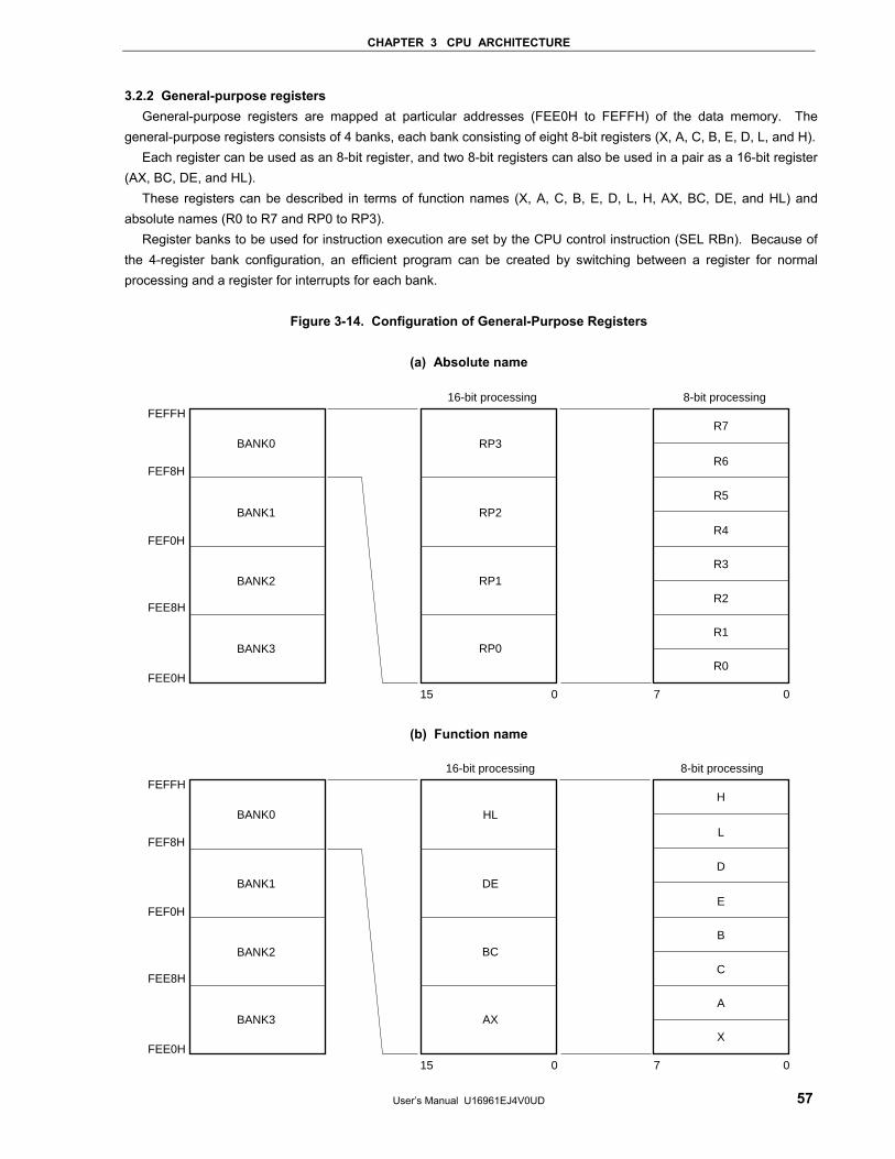
CHAPTER 3 CPU ARCHITECTURE
User’s Manual U16961EJ4V0UD 57
3.2.2 General-purpose registers General-purpose registers are mapped at particular addresses (FEE0H to FEFFH) of the data memory. The
general-purpose registers consists of 4 banks, each bank consisting of eight 8-bit registers (X, A, C, B, E, D, L, and H). Each register can be used as an 8-bit register, and two 8-bit registers can also be used in a pair as a 16-bit register
(AX, BC, DE, and HL). These registers can be described in terms of function names (X, A, C, B, E, D, L, H, AX, BC, DE, and HL) and
absolute names (R0 to R7 and RP0 to RP3). Register banks to be used for instruction execution are set by the CPU control instruction (SEL RBn). Because of
the 4-register bank configuration, an efficient program can be created by switching between a register for normal processing and a register for interrupts for each bank.
Figure 3-14. Configuration of General-Purpose Registers
(a) Absolute name
BANK0
BANK1
BANK2
BANK3
FEFFH
FEF8H
FEE0H
RP3
RP2
RP1
RP0
R7
15 0 7 0
R6
R5
R4
R3
R2
R1
R0
16-bit processing 8-bit processing
FEF0H
FEE8H
(b) Function name
BANK0
BANK1
BANK2
BANK3
FEFFH
FEF8H
FEE0H
HL
DE
BC
AX
H
15 0 7 0
L
D
E
B
C
A
X
16-bit processing 8-bit processing
FEF0H
FEE8H
CHAPTER 3 CPU ARCHITECTURE
User’s Manual U16961EJ4V0UD 58
3.2.3 Special function registers (SFRs) Unlike a general-purpose register, each special function register has a special function. SFRs are allocated to the FF00H to FFFFH area. Special function registers can be manipulated like general-purpose registers, using operation, transfer and bit
manipulation instructions. The manipulatable bit units, 1, 8, and 16, depend on the special function register type. Each manipulation bit unit can be specified as follows.
• 1-bit manipulation Describe the symbol reserved by the assembler for the 1-bit manipulation instruction operand (sfr.bit). This manipulation can also be specified with an address. • 8-bit manipulation Describe the symbol reserved by the assembler for the 8-bit manipulation instruction operand (sfr). This manipulation can also be specified with an address. • 16-bit manipulation Describe the symbol reserved by the assembler for the 16-bit manipulation instruction operand (sfrp). When specifying an address, describe an even address.
Table 3-5 gives a list of the special function registers. The meanings of items in the table are as follows.
• Symbol Symbol indicating the address of a special function register. It is a reserved word in the RA78K0, and is defined
as an sfr variable using the #pragma sfr directive in the CC78K0. When using the RA78K0, ID78K0-NS, ID78K0, or SM78K0, symbols can be written as an instruction operand.
• R/W Indicates whether the corresponding special function register can be read or written. R/W: Read/write enable R: Read only W: Write only • Manipulatable bit units Indicates the manipulatable bit unit (1, 8, or 16). “−” indicates a bit unit for which manipulation is not possible. • After reset Indicates each register status upon RESET input.
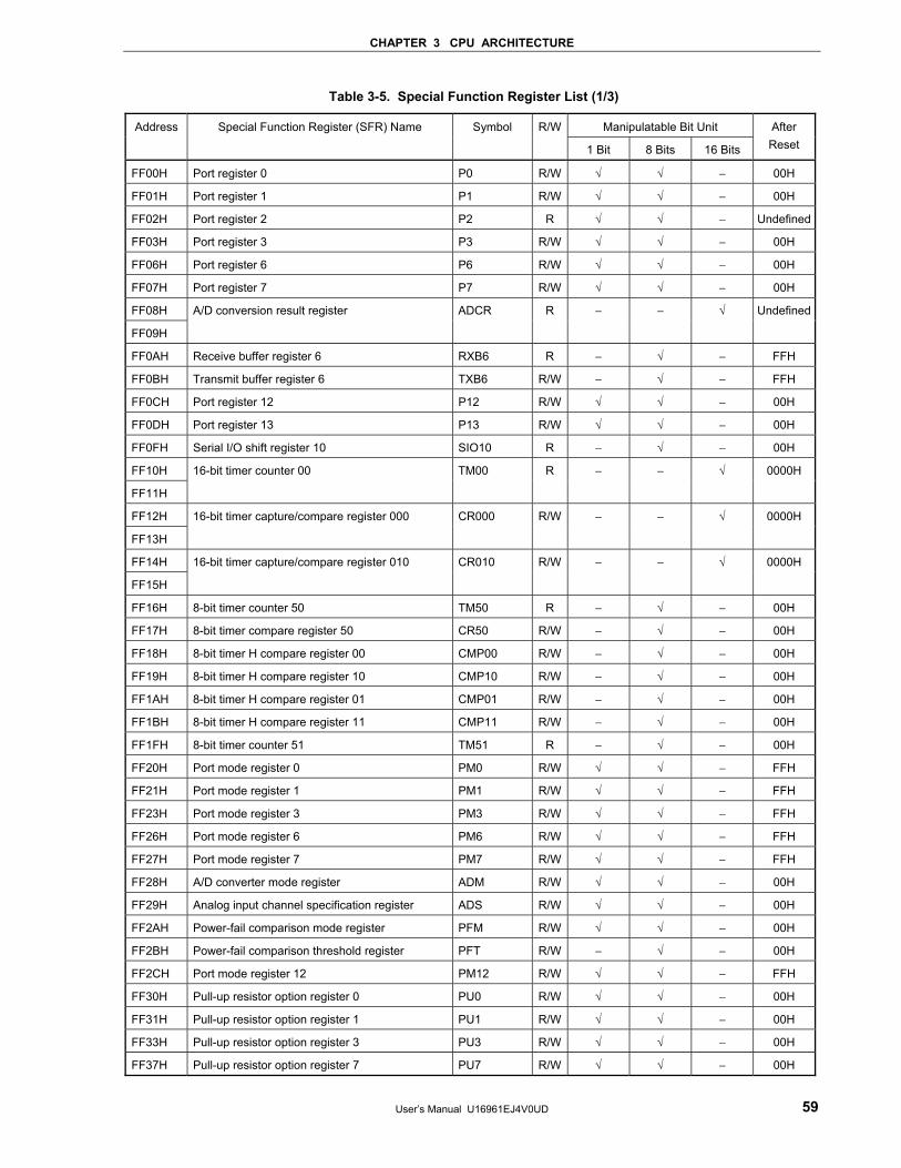
CHAPTER 3 CPU ARCHITECTURE
User’s Manual U16961EJ4V0UD 59
Table 3-5. Special Function Register List (1/3)
Manipulatable Bit Unit Address Special Function Register (SFR) Name Symbol R/W
1 Bit 8 Bits 16 Bits
After Reset
FF00H Port register 0 P0 R/W √ √ − 00H
FF01H Port register 1 P1 R/W √ √ − 00H
FF02H Port register 2 P2 R √ √ − Undefined
FF03H Port register 3 P3 R/W √ √ − 00H
FF06H Port register 6 P6 R/W √ √ − 00H
FF07H Port register 7 P7 R/W √ √ − 00H
FF08H
FF09H
A/D conversion result register ADCR R − − √ Undefined
FF0AH Receive buffer register 6 RXB6 R − √ − FFH
FF0BH Transmit buffer register 6 TXB6 R/W − √ − FFH
FF0CH Port register 12 P12 R/W √ √ − 00H
FF0DH Port register 13 P13 R/W √ √ − 00H
FF0FH Serial I/O shift register 10 SIO10 R − √ − 00H
FF10H
FF11H
16-bit timer counter 00 TM00 R − − √ 0000H
FF12H
FF13H
16-bit timer capture/compare register 000 CR000 R/W − − √ 0000H
FF14H
FF15H
16-bit timer capture/compare register 010 CR010 R/W − − √ 0000H
FF16H 8-bit timer counter 50 TM50 R − √ − 00H
FF17H 8-bit timer compare register 50 CR50 R/W − √ − 00H
FF18H 8-bit timer H compare register 00 CMP00 R/W − √ − 00H
FF19H 8-bit timer H compare register 10 CMP10 R/W − √ − 00H
FF1AH 8-bit timer H compare register 01 CMP01 R/W − √ − 00H
FF1BH 8-bit timer H compare register 11 CMP11 R/W − √ − 00H
FF1FH 8-bit timer counter 51 TM51 R − √ − 00H
FF20H Port mode register 0 PM0 R/W √ √ − FFH
FF21H Port mode register 1 PM1 R/W √ √ − FFH
FF23H Port mode register 3 PM3 R/W √ √ − FFH
FF26H Port mode register 6 PM6 R/W √ √ − FFH
FF27H Port mode register 7 PM7 R/W √ √ − FFH
FF28H A/D converter mode register ADM R/W √ √ − 00H
FF29H Analog input channel specification register ADS R/W √ √ − 00H
FF2AH Power-fail comparison mode register PFM R/W √ √ − 00H
FF2BH Power-fail comparison threshold register PFT R/W − √ − 00H
FF2CH Port mode register 12 PM12 R/W √ √ − FFH
FF30H Pull-up resistor option register 0 PU0 R/W √ √ − 00H
FF31H Pull-up resistor option register 1 PU1 R/W √ √ − 00H
FF33H Pull-up resistor option register 3 PU3 R/W √ √ − 00H
FF37H Pull-up resistor option register 7 PU7 R/W √ √ − 00H
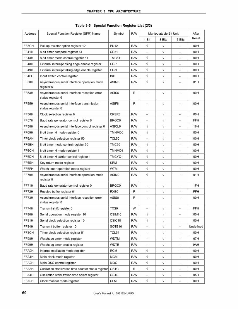
CHAPTER 3 CPU ARCHITECTURE
User’s Manual U16961EJ4V0UD 60
Table 3-5. Special Function Register List (2/3)
Manipulatable Bit Unit Address Special Function Register (SFR) Name Symbol R/W
1 Bit 8 Bits 16 Bits
After Reset
FF3CH Pull-up resistor option register 12 PU12 R/W √ √ − 00H
FF41H 8-bit timer compare register 51 CR51 R/W − √ − 00H
FF43H 8-bit timer mode control register 51 TMC51 R/W √ √ − 00H
FF48H External interrupt rising edge enable register EGP R/W √ √ − 00H
FF49H External interrupt falling edge enable register EGN R/W √ √ − 00H
FF4FH Input switch control register ISC R/W √ √ − 00H
FF50H Asynchronous serial interface operation mode register 6
ASIM6 R/W √ √ − 01H
FF53H Asynchronous serial interface reception error status register 6
ASIS6 R − √ − 00H
FF55H Asynchronous serial interface transmission status register 6
ASIF6 R − √ − 00H
FF56H Clock selection register 6 CKSR6 R/W − √ − 00H
FF57H Baud rate generator control register 6 BRGC6 R/W − √ − FFH
FF58H Asynchronous serial interface control register 6 ASICL6 R/W √ √ − 16H
FF69H 8-bit timer H mode register 0 TMHMD0 R/W √ √ − 00H
FF6AH Timer clock selection register 50 TCL50 R/W − √ − 00H
FF6BH 8-bit timer mode control register 50 TMC50 R/W √ √ − 00H
FF6CH 8-bit timer H mode register 1 TMHMD1 R/W √ √ − 00H
FF6DH 8-bit timer H carrier control register 1 TMCYC1 R/W √ √ − 00H
FF6EH Key return mode register KRM R/W √ √ − 00H
FF6FH Watch timer operation mode register WTM R/W √ √ − 00H
FF70H Asynchronous serial interface operation mode register 0
ASIM0 R/W √ √ − 01H
FF71H Baud rate generator control register 0 BRGC0 R/W − √ − 1FH
FF72H Receive buffer register 0 RXB0 R − √ − FFH
FF73H Asynchronous serial interface reception error status register 0
ASIS0 R − √ − 00H
FF74H Transmit shift register 0 TXS0 W − √ − FFH
FF80H Serial operation mode register 10 CSIM10 R/W √ √ − 00H
FF81H Serial clock selection register 10 CSIC10 R/W √ √ − 00H
FF84H Transmit buffer register 10 SOTB10 R/W − √ − Undefined
FF8CH Timer clock selection register 51 TCL51 R/W − √ − 00H
FF98H Watchdog timer mode register WDTM R/W − √ − 67H
FF99H Watchdog timer enable register WDTE R/W − √ − 9AH
FFA0H Internal oscillation mode register RCM R/W √ √ − 00H
FFA1H Main clock mode register MCM R/W √ √ − 00H
FFA2H Main OSC control register MOC R/W √ √ − 00H
FFA3H Oscillation stabilization time counter status register OSTC R √ √ − 00H
FFA4H Oscillation stabilization time select register OSTS R/W − √ − 05H
FFA9H Clock monitor mode register CLM R/W √ √ − 00H
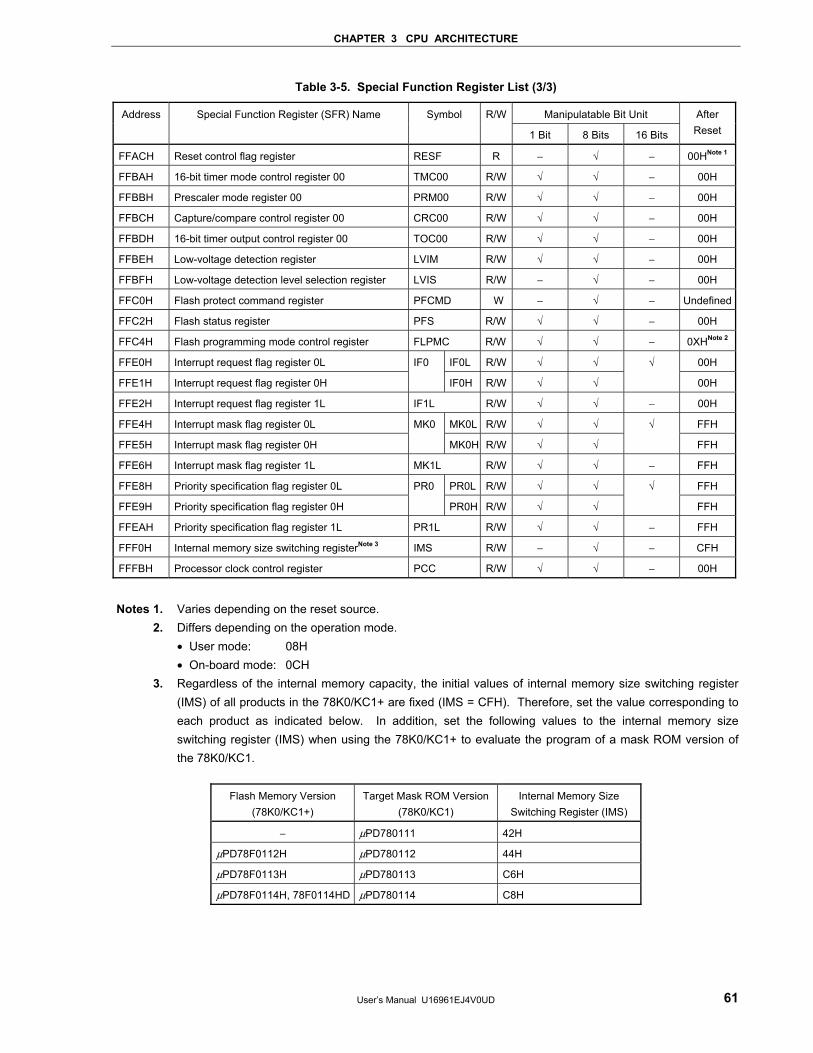
CHAPTER 3 CPU ARCHITECTURE
User’s Manual U16961EJ4V0UD 61
Table 3-5. Special Function Register List (3/3)
Manipulatable Bit Unit Address Special Function Register (SFR) Name Symbol R/W
1 Bit 8 Bits 16 Bits
After Reset
FFACH Reset control flag register RESF R − √ − 00HNote 1
FFBAH 16-bit timer mode control register 00 TMC00 R/W √ √ − 00H
FFBBH Prescaler mode register 00 PRM00 R/W √ √ − 00H
FFBCH Capture/compare control register 00 CRC00 R/W √ √ − 00H
FFBDH 16-bit timer output control register 00 TOC00 R/W √ √ − 00H
FFBEH Low-voltage detection register LVIM R/W √ √ − 00H
FFBFH Low-voltage detection level selection register LVIS R/W − √ − 00H
FFC0H Flash protect command register PFCMD W − √ − Undefined
FFC2H Flash status register PFS R/W √ √ − 00H
FFC4H Flash programming mode control register FLPMC R/W √ √ − 0XHNote 2
FFE0H Interrupt request flag register 0L IF0 IF0L R/W √ √ √ 00H
FFE1H Interrupt request flag register 0H IF0H R/W √ √ 00H
FFE2H Interrupt request flag register 1L IF1L R/W √ √ − 00H
FFE4H Interrupt mask flag register 0L MK0 MK0L R/W √ √ √ FFH
FFE5H Interrupt mask flag register 0H MK0H R/W √ √ FFH
FFE6H Interrupt mask flag register 1L MK1L R/W √ √ − FFH
FFE8H Priority specification flag register 0L PR0 PR0L R/W √ √ √ FFH
FFE9H Priority specification flag register 0H PR0H R/W √ √ FFH
FFEAH Priority specification flag register 1L PR1L R/W √ √ − FFH
FFF0H Internal memory size switching registerNote 3 IMS R/W − √ − CFH
FFFBH Processor clock control register PCC R/W √ √ − 00H
Notes 1. Varies depending on the reset source. 2. Differs depending on the operation mode. • User mode: 08H • On-board mode: 0CH 3. Regardless of the internal memory capacity, the initial values of internal memory size switching register
(IMS) of all products in the 78K0/KC1+ are fixed (IMS = CFH). Therefore, set the value corresponding to each product as indicated below. In addition, set the following values to the internal memory size switching register (IMS) when using the 78K0/KC1+ to evaluate the program of a mask ROM version of the 78K0/KC1.
Flash Memory Version
(78K0/KC1+) Target Mask ROM Version
(78K0/KC1) Internal Memory Size
Switching Register (IMS)
− μPD780111 42H
μPD78F0112H μPD780112 44H
μPD78F0113H μPD780113 C6H
μPD78F0114H, 78F0114HD μPD780114 C8H
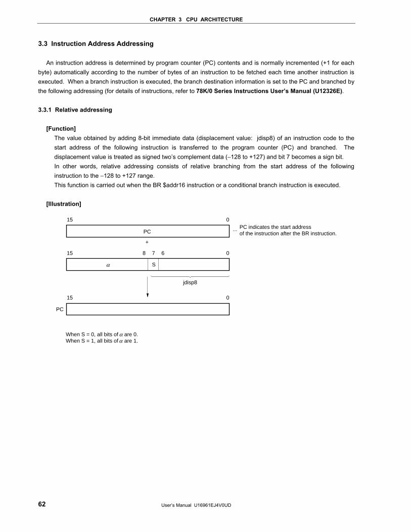
CHAPTER 3 CPU ARCHITECTURE
User’s Manual U16961EJ4V0UD 62
3.3 Instruction Address Addressing
An instruction address is determined by program counter (PC) contents and is normally incremented (+1 for each byte) automatically according to the number of bytes of an instruction to be fetched each time another instruction is executed. When a branch instruction is executed, the branch destination information is set to the PC and branched by the following addressing (for details of instructions, refer to 78K/0 Series Instructions User’s Manual (U12326E). 3.3.1 Relative addressing
[Function] The value obtained by adding 8-bit immediate data (displacement value: jdisp8) of an instruction code to the start address of the following instruction is transferred to the program counter (PC) and branched. The displacement value is treated as signed two’s complement data (−128 to +127) and bit 7 becomes a sign bit. In other words, relative addressing consists of relative branching from the start address of the following instruction to the −128 to +127 range. This function is carried out when the BR $addr16 instruction or a conditional branch instruction is executed.
[Illustration]
15 0
PC
+
15 08 7 6
S
15 0
PC
α
jdisp8
When S = 0, all bits of are 0.When S = 1, all bits of are 1.
PC indicates the start addressof the instruction after the BR instruction.
...
αα
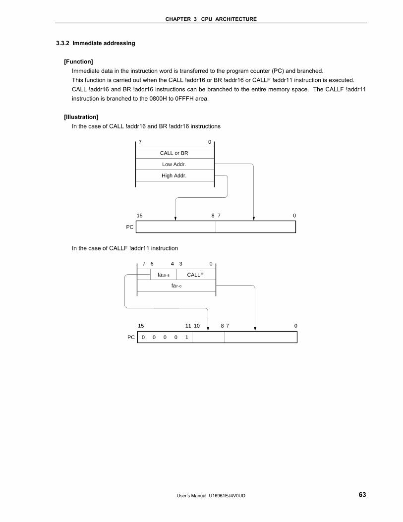
CHAPTER 3 CPU ARCHITECTURE
User’s Manual U16961EJ4V0UD 63
3.3.2 Immediate addressing
[Function] Immediate data in the instruction word is transferred to the program counter (PC) and branched. This function is carried out when the CALL !addr16 or BR !addr16 or CALLF !addr11 instruction is executed. CALL !addr16 and BR !addr16 instructions can be branched to the entire memory space. The CALLF !addr11 instruction is branched to the 0800H to 0FFFH area.
[Illustration]
In the case of CALL !addr16 and BR !addr16 instructions
15 0
PC
8 7
7 0
CALL or BR
Low Addr.
High Addr.
In the case of CALLF !addr11 instruction
15 0
PC
8 7
7 0
fa10–8
11 10
0 0 0 0 1
6 4 3
CALLF
fa7–0
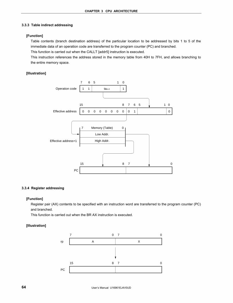
CHAPTER 3 CPU ARCHITECTURE
User’s Manual U16961EJ4V0UD 64
3.3.3 Table indirect addressing
[Function] Table contents (branch destination address) of the particular location to be addressed by bits 1 to 5 of the immediate data of an operation code are transferred to the program counter (PC) and branched. This function is carried out when the CALLT [addr5] instruction is executed. This instruction references the address stored in the memory table from 40H to 7FH, and allows branching to the entire memory space.
[Illustration]
15 1
15 0
PC
7 0
Low Addr.
High Addr.
Memory (Table)
Effective address+1
Effective address 0 10 0 0 0 0 0 0 0
8 7
8 7
6 5 0
0
11 1
7 6 5 1 0
ta4–0Operation code
3.3.4 Register addressing
[Function] Register pair (AX) contents to be specified with an instruction word are transferred to the program counter (PC) and branched. This function is carried out when the BR AX instruction is executed.
[Illustration]
7 0
rp
0 7
A X
15 0
PC
8 7
CHAPTER 3 CPU ARCHITECTURE
User’s Manual U16961EJ4V0UD 65
3.4 Operand Address Addressing
The following methods are available to specify the register and memory (addressing) to undergo manipulation during instruction execution. 3.4.1 Implied addressing
[Function] The register that functions as an accumulator (A and AX) among the general-purpose registers is automatically (implicitly) addressed. Of the 78K0/KC1+ instruction words, the following instructions employ implied addressing.
Instruction Register to Be Specified by Implied Addressing
MULU A register for multiplicand and AX register for product storage
DIVUW AX register for dividend and quotient storage
ADJBA/ADJBS A register for storage of numeric values that become decimal correction targets
ROR4/ROL4 A register for storage of digit data that undergoes digit rotation
[Operand format]
Because implied addressing can be automatically employed with an instruction, no particular operand format is necessary.
[Description example]
In the case of MULU X With an 8-bit × 8-bit multiply instruction, the product of A register and X register is stored in AX. In this example, the A and AX registers are specified by implied addressing.
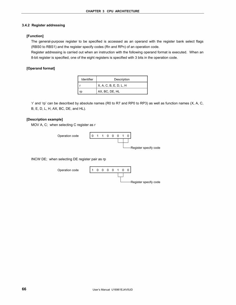
CHAPTER 3 CPU ARCHITECTURE
User’s Manual U16961EJ4V0UD 66
3.4.2 Register addressing
[Function] The general-purpose register to be specified is accessed as an operand with the register bank select flags (RBS0 to RBS1) and the register specify codes (Rn and RPn) of an operation code. Register addressing is carried out when an instruction with the following operand format is executed. When an 8-bit register is specified, one of the eight registers is specified with 3 bits in the operation code.
[Operand format]
Identifier Description
r X, A, C, B, E, D, L, H
rp AX, BC, DE, HL
‘r’ and ‘rp’ can be described by absolute names (R0 to R7 and RP0 to RP3) as well as function names (X, A, C, B, E, D, L, H, AX, BC, DE, and HL).
[Description example]
MOV A, C; when selecting C register as r
Operation code 0 1 1 0 0 0 1 0
Register specify code
INCW DE; when selecting DE register pair as rp
Operation code 1 0 0 0 0 1 0 0
Register specify code
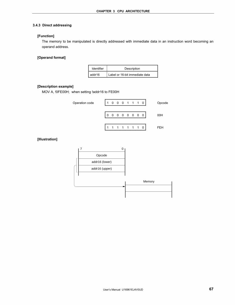
CHAPTER 3 CPU ARCHITECTURE
User’s Manual U16961EJ4V0UD 67
3.4.3 Direct addressing
[Function] The memory to be manipulated is directly addressed with immediate data in an instruction word becoming an operand address.
[Operand format]
Identifier Description
addr16 Label or 16-bit immediate data
[Description example]
MOV A, !0FE00H; when setting !addr16 to FE00H
Operation code 1 0 0 0 1 1 1 0 Opcode
0 0 0 0 0 0 0 0 00H
1 1 1 1 1 1 1 0 FEH
[Illustration]
Memory
07
addr16 (lower)
addr16 (upper)
Opcode
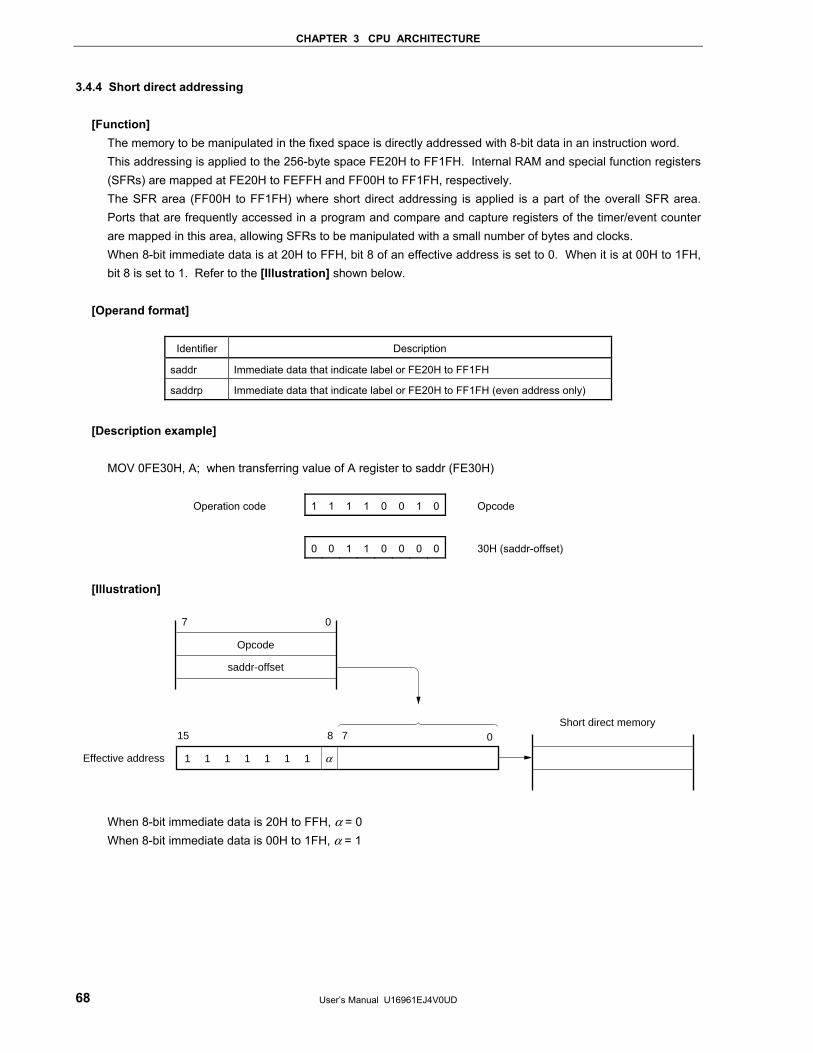
CHAPTER 3 CPU ARCHITECTURE
User’s Manual U16961EJ4V0UD 68
3.4.4 Short direct addressing
[Function] The memory to be manipulated in the fixed space is directly addressed with 8-bit data in an instruction word. This addressing is applied to the 256-byte space FE20H to FF1FH. Internal RAM and special function registers (SFRs) are mapped at FE20H to FEFFH and FF00H to FF1FH, respectively. The SFR area (FF00H to FF1FH) where short direct addressing is applied is a part of the overall SFR area. Ports that are frequently accessed in a program and compare and capture registers of the timer/event counter are mapped in this area, allowing SFRs to be manipulated with a small number of bytes and clocks. When 8-bit immediate data is at 20H to FFH, bit 8 of an effective address is set to 0. When it is at 00H to 1FH, bit 8 is set to 1. Refer to the [Illustration] shown below.
[Operand format]
Identifier Description
saddr Immediate data that indicate label or FE20H to FF1FH
saddrp Immediate data that indicate label or FE20H to FF1FH (even address only)
[Description example]
MOV 0FE30H, A; when transferring value of A register to saddr (FE30H)
Operation code 1 1 1 1 0 0 1 0 Opcode
0 0 1 1 0 0 0 0 30H (saddr-offset)
[Illustration]
15 0Short direct memory
Effective address 1 1 1 1 1 1 1
8 7
07
Opcode
saddr-offset
α
When 8-bit immediate data is 20H to FFH, α = 0 When 8-bit immediate data is 00H to 1FH, α = 1
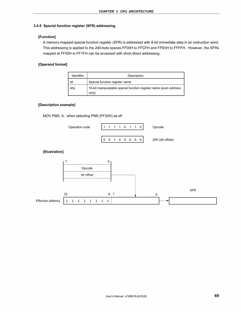
CHAPTER 3 CPU ARCHITECTURE
User’s Manual U16961EJ4V0UD 69
3.4.5 Special function register (SFR) addressing
[Function] A memory-mapped special function register (SFR) is addressed with 8-bit immediate data in an instruction word. This addressing is applied to the 240-byte spaces FF00H to FFCFH and FFE0H to FFFFH. However, the SFRs mapped at FF00H to FF1FH can be accessed with short direct addressing.
[Operand format]
Identifier Description
sfr Special function register name
sfrp 16-bit manipulatable special function register name (even address only)
[Description example]
MOV PM0, A; when selecting PM0 (FF20H) as sfr
Operation code 1 1 1 1 0 1 1 0 Opcode
0 0 1 0 0 0 0 0 20H (sfr-offset)
[Illustration]
15 0SFR
Effective address 1 1 1 1 1 1 1
8 7
07
Opcode
sfr-offset
1
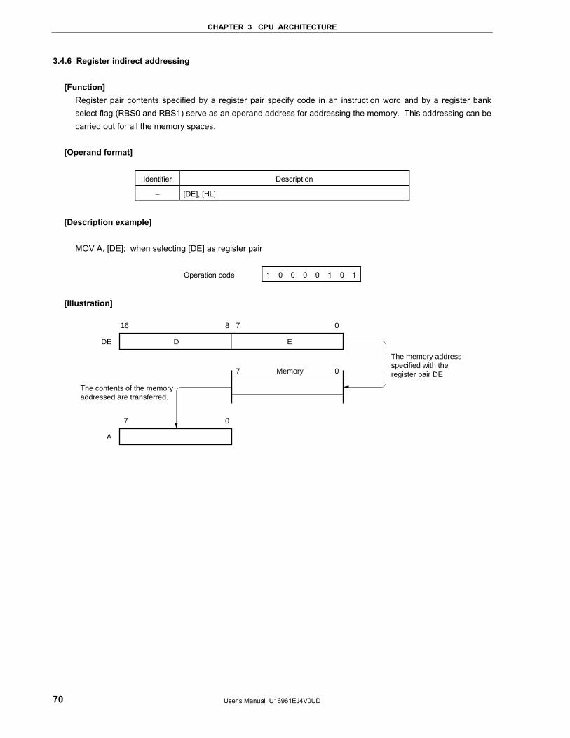
CHAPTER 3 CPU ARCHITECTURE
User’s Manual U16961EJ4V0UD 70
3.4.6 Register indirect addressing
[Function] Register pair contents specified by a register pair specify code in an instruction word and by a register bank select flag (RBS0 and RBS1) serve as an operand address for addressing the memory. This addressing can be carried out for all the memory spaces.
[Operand format]
Identifier Description
− [DE], [HL]
[Description example]
MOV A, [DE]; when selecting [DE] as register pair
Operation code 1 0 0 0 0 1 0 1
[Illustration]
16 08
D
7
E
07
7 0
A
DE
The contents of the memoryaddressed are transferred.
Memory
The memory addressspecified with theregister pair DE
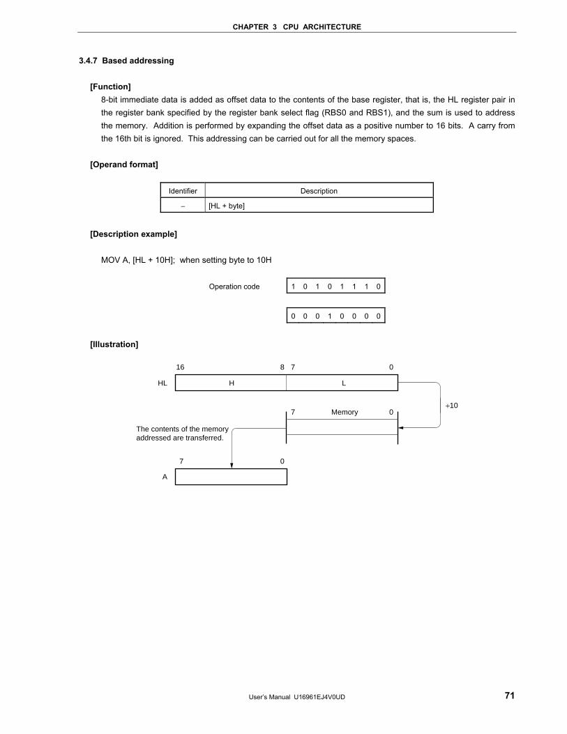
CHAPTER 3 CPU ARCHITECTURE
User’s Manual U16961EJ4V0UD 71
3.4.7 Based addressing
[Function] 8-bit immediate data is added as offset data to the contents of the base register, that is, the HL register pair in the register bank specified by the register bank select flag (RBS0 and RBS1), and the sum is used to address the memory. Addition is performed by expanding the offset data as a positive number to 16 bits. A carry from the 16th bit is ignored. This addressing can be carried out for all the memory spaces.
[Operand format]
Identifier Description
− [HL + byte]
[Description example]
MOV A, [HL + 10H]; when setting byte to 10H
Operation code 1 0 1 0 1 1 1 0
0 0 0 1 0 0 0 0
[Illustration]
16 08
H
7
L
07
7 0
A
HL
The contents of the memoryaddressed are transferred.
Memory+10
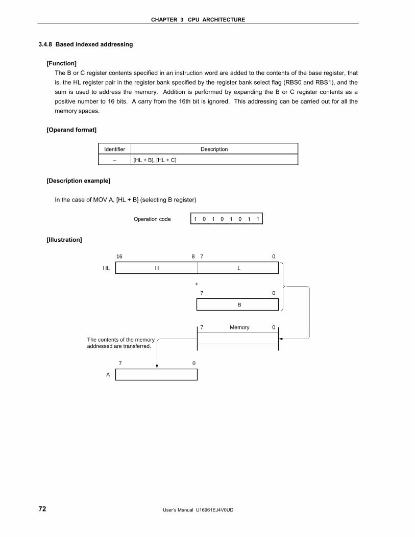
CHAPTER 3 CPU ARCHITECTURE
User’s Manual U16961EJ4V0UD 72
3.4.8 Based indexed addressing
[Function] The B or C register contents specified in an instruction word are added to the contents of the base register, that is, the HL register pair in the register bank specified by the register bank select flag (RBS0 and RBS1), and the sum is used to address the memory. Addition is performed by expanding the B or C register contents as a positive number to 16 bits. A carry from the 16th bit is ignored. This addressing can be carried out for all the memory spaces.
[Operand format]
Identifier Description
− [HL + B], [HL + C]
[Description example]
In the case of MOV A, [HL + B] (selecting B register)
Operation code 1 0 1 0 1 0 1 1
[Illustration]
16 0
H
78
L
07
B
+
07
7 0
A
HL
The contents of the memoryaddressed are transferred.
Memory
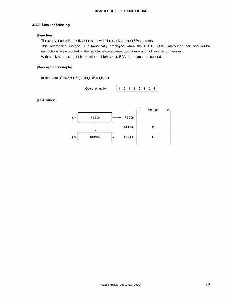
CHAPTER 3 CPU ARCHITECTURE
User’s Manual U16961EJ4V0UD 73
3.4.9 Stack addressing
[Function] The stack area is indirectly addressed with the stack pointer (SP) contents. This addressing method is automatically employed when the PUSH, POP, subroutine call and return instructions are executed or the register is saved/reset upon generation of an interrupt request. With stack addressing, only the internal high-speed RAM area can be accessed.
[Description example]
In the case of PUSH DE (saving DE register)
Operation code 1 0 1 1 0 1 0 1
[Illustration]
E
FEE0HSP
SP
FEE0H
FEDFH
FEDEH
D
Memory 07
FEDEH
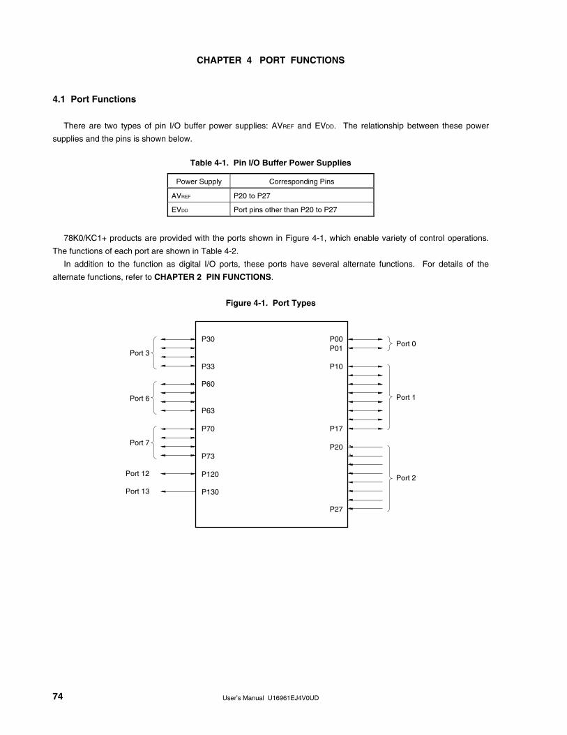
User’s Manual U16961EJ4V0UD 74
CHAPTER 4 PORT FUNCTIONS
4.1 Port Functions
There are two types of pin I/O buffer power supplies: AVREF and EVDD. The relationship between these power
supplies and the pins is shown below.
Table 4-1. Pin I/O Buffer Power Supplies
Power Supply Corresponding Pins
AVREF P20 to P27
EVDD Port pins other than P20 to P27
78K0/KC1+ products are provided with the ports shown in Figure 4-1, which enable variety of control operations.
The functions of each port are shown in Table 4-2.
In addition to the function as digital I/O ports, these ports have several alternate functions. For details of the
alternate functions, refer to CHAPTER 2 PIN FUNCTIONS.
Figure 4-1. Port Types
Port 2
P20
P27
Port 3
P30
P33
Port 0P00P01
Port 1
P10
P17
Port 6
P60
P63
Port 7
P70
P73
P120Port 12
P130Port 13
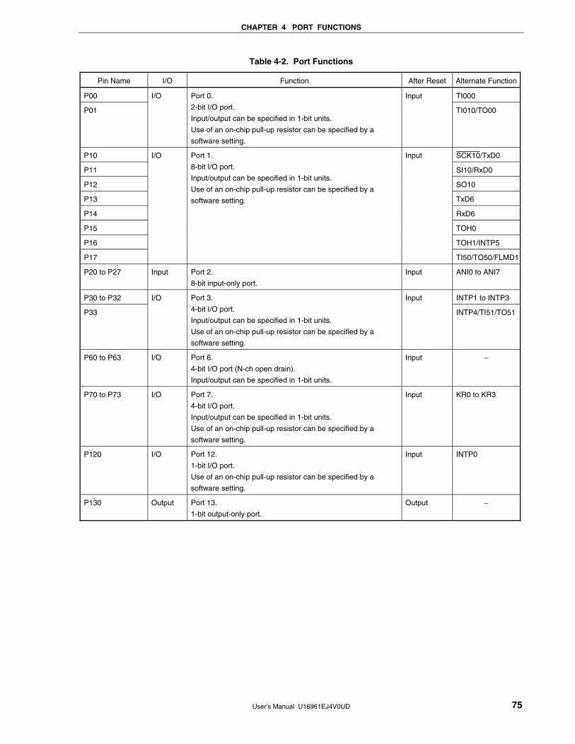
CHAPTER 4 PORT FUNCTIONS
User’s Manual U16961EJ4V0UD 75
Table 4-2. Port Functions
Pin Name I/O Function After Reset Alternate Function
P00 TI000
P01
I/O Port 0.
2-bit I/O port.
Input/output can be specified in 1-bit units.
Use of an on-chip pull-up resistor can be specified by a
software setting.
Input
TI010/TO00
P10 SCK10/TxD0
P11 SI10/RxD0
P12 SO10
P13 TxD6
P14 RxD6
P15 TOH0
P16 TOH1/INTP5
P17
I/O Port 1.
8-bit I/O port.
Input/output can be specified in 1-bit units.
Use of an on-chip pull-up resistor can be specified by a
software setting.
Input
TI50/TO50/FLMD1
P20 to P27 Input Port 2.
8-bit input-only port.
Input ANI0 to ANI7
P30 to P32 INTP1 to INTP3
P33
I/O Port 3.
4-bit I/O port.
Input/output can be specified in 1-bit units.
Use of an on-chip pull-up resistor can be specified by a
software setting.
Input
INTP4/TI51/TO51
P60 to P63 I/O Port 6.
4-bit I/O port (N-ch open drain).
Input/output can be specified in 1-bit units.
Input −
P70 to P73 I/O Port 7.
4-bit I/O port.
Input/output can be specified in 1-bit units.
Use of an on-chip pull-up resistor can be specified by a
software setting.
Input KR0 to KR3
P120 I/O Port 12.
1-bit I/O port.
Use of an on-chip pull-up resistor can be specified by a
software setting.
Input INTP0
P130 Output Port 13.
1-bit output-only port.
Output −
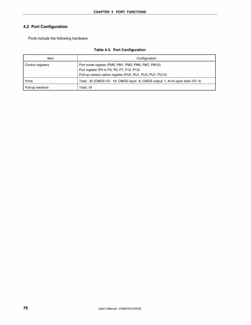
CHAPTER 4 PORT FUNCTIONS
User’s Manual U16961EJ4V0UD 76
4.2 Port Configuration
Ports include the following hardware.
Table 4-3. Port Configuration
Item Configuration
Control registers Port mode register (PM0, PM1, PM3, PM6, PM7, PM12)
Port register (P0 to P3, P6, P7, P12, P13)
Pull-up resistor option register (PU0, PU1, PU3, PU7, PU12)
Ports Total: 32 (CMOS I/O: 19, CMOS input: 8, CMOS output: 1, N-ch open drain I/O: 4)
Pull-up resistors Total: 19
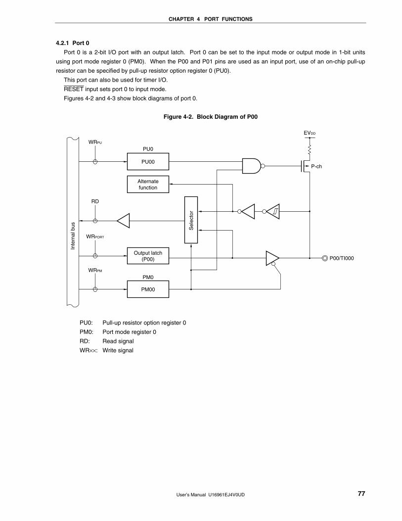
CHAPTER 4 PORT FUNCTIONS
User’s Manual U16961EJ4V0UD 77
4.2.1 Port 0
Port 0 is a 2-bit I/O port with an output latch. Port 0 can be set to the input mode or output mode in 1-bit units
using port mode register 0 (PM0). When the P00 and P01 pins are used as an input port, use of an on-chip pull-up
resistor can be specified by pull-up resistor option register 0 (PU0).
This port can also be used for timer I/O.
RESET input sets port 0 to input mode.
Figures 4-2 and 4-3 show block diagrams of port 0.
Figure 4-2. Block Diagram of P00
P00/TI000
WRPU
RD
WRPORT
WRPM
PU00
PU0
Alternatefunction
Output latch(P00)
PM00
PM0
EVDD
P-ch
Sel
ecto
r
Inte
rnal
bus
PU0: Pull-up resistor option register 0
PM0: Port mode register 0
RD: Read signal
WR××: Write signal
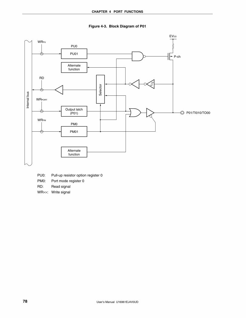
CHAPTER 4 PORT FUNCTIONS
User’s Manual U16961EJ4V0UD 78
Figure 4-3. Block Diagram of P01
P01/TI010/TO00
WRPU
RD
WRPORT
WRPM
PU01
Alternatefunction
Output latch(P01)
PM01
PU0
PM0
Alternatefunction
EVDD
P-ch
Sel
ecto
r
Inte
rnal
bus
PU0: Pull-up resistor option register 0
PM0: Port mode register 0
RD: Read signal
WR××: Write signal
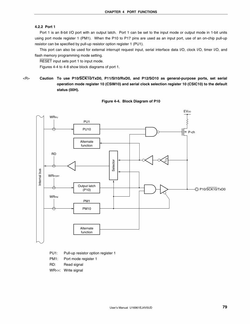
CHAPTER 4 PORT FUNCTIONS
User’s Manual U16961EJ4V0UD 79
4.2.2 Port 1
Port 1 is an 8-bit I/O port with an output latch. Port 1 can be set to the input mode or output mode in 1-bit units
using port mode register 1 (PM1). When the P10 to P17 pins are used as an input port, use of an on-chip pull-up
resistor can be specified by pull-up resistor option register 1 (PU1).
This port can also be used for external interrupt request input, serial interface data I/O, clock I/O, timer I/O, and
flash memory programming mode setting.
RESET input sets port 1 to input mode.
Figures 4-4 to 4-8 show block diagrams of port 1.
Caution To use P10/SCK10/TxD0, P11/SI10/RxD0, and P12/SO10 as general-purpose ports, set serial
operation mode register 10 (CSIM10) and serial clock selection register 10 (CSIC10) to the default
status (00H).
Figure 4-4. Block Diagram of P10
P10/SCK10/TxD0
WRPU
RD
WRPORT
WRPM
PU10
Alternatefunction
Output latch(P10)
PM10
PU1
PM1
Alternatefunction
EVDD
P-ch
Sel
ecto
r
Inte
rnal
bus
PU1: Pull-up resistor option register 1
PM1: Port mode register 1
RD: Read signal
WR××: Write signal
<R>
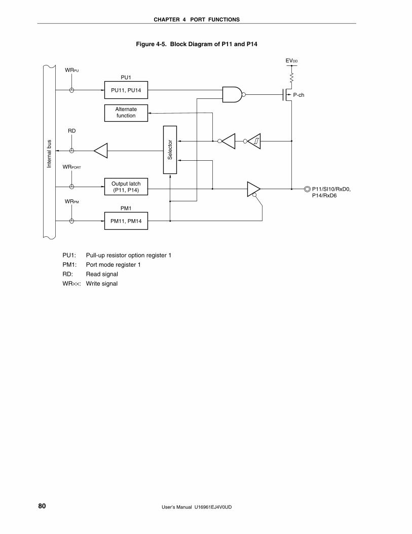
CHAPTER 4 PORT FUNCTIONS
User’s Manual U16961EJ4V0UD 80
Figure 4-5. Block Diagram of P11 and P14
P11/SI10/RxD0,P14/RxD6
WRPU
RD
WRPORT
WRPM
PU11, PU14
Alternatefunction
Output latch(P11, P14)
PM11, PM14
PU1
PM1
EVDD
P-ch
Sel
ecto
r
Inte
rnal
bus
PU1: Pull-up resistor option register 1
PM1: Port mode register 1
RD: Read signal
WR××: Write signal
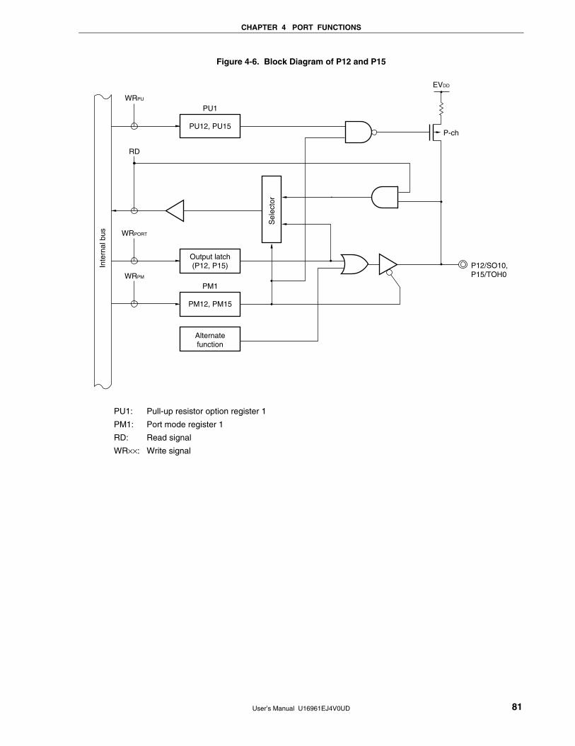
CHAPTER 4 PORT FUNCTIONS
User’s Manual U16961EJ4V0UD 81
Figure 4-6. Block Diagram of P12 and P15
P12/SO10,P15/TOH0
WRPU
RD
WRPORT
WRPM
PU12, PU15
Output latch(P12, P15)
PM12, PM15
PU1
PM1
Alternatefunction
EVDD
P-ch
Sel
ecto
r
Inte
rnal
bus
PU1: Pull-up resistor option register 1
PM1: Port mode register 1
RD: Read signal
WR××: Write signal
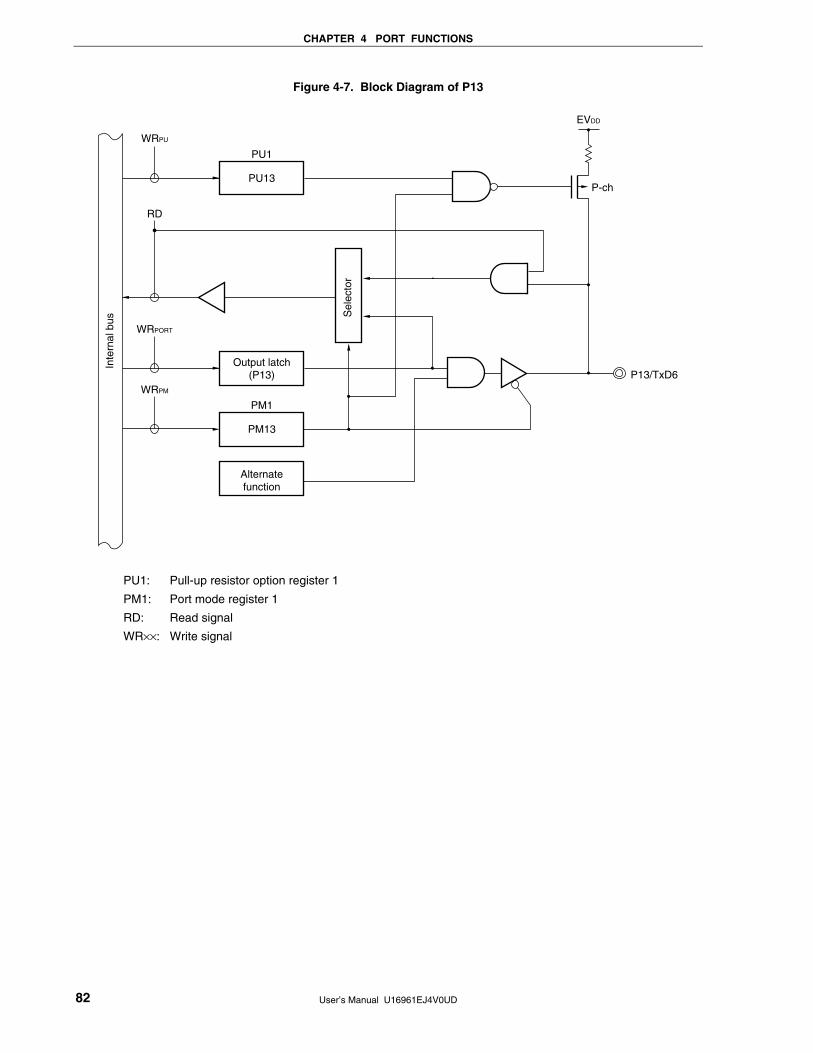
CHAPTER 4 PORT FUNCTIONS
User’s Manual U16961EJ4V0UD 82
Figure 4-7. Block Diagram of P13
P13/TxD6
WRPU
RD
WRPORT
WRPM
PU13
Output latch(P13)
PM13
PU1
PM1
Alternatefunction
EVDD
P-ch
Inte
rnal
bus
Sel
ecto
r
PU1: Pull-up resistor option register 1
PM1: Port mode register 1
RD: Read signal
WR××: Write signal
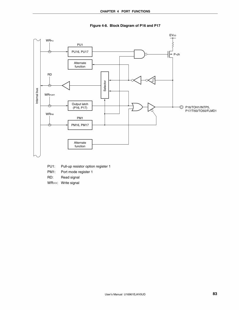
CHAPTER 4 PORT FUNCTIONS
User’s Manual U16961EJ4V0UD 83
Figure 4-8. Block Diagram of P16 and P17
P16/TOH1/INTP5,P17/TI50/TO50/FLMD1
WRPU
RD
WRPORT
WRPM
PU16, PU17
Alternatefunction
Output latch(P16, P17)
PM16, PM17
PU1
PM1
Alternatefunction
EVDD
P-ch
Sel
ecto
r
Inte
rnal
bus
PU1: Pull-up resistor option register 1
PM1: Port mode register 1
RD: Read signal
WR××: Write signal
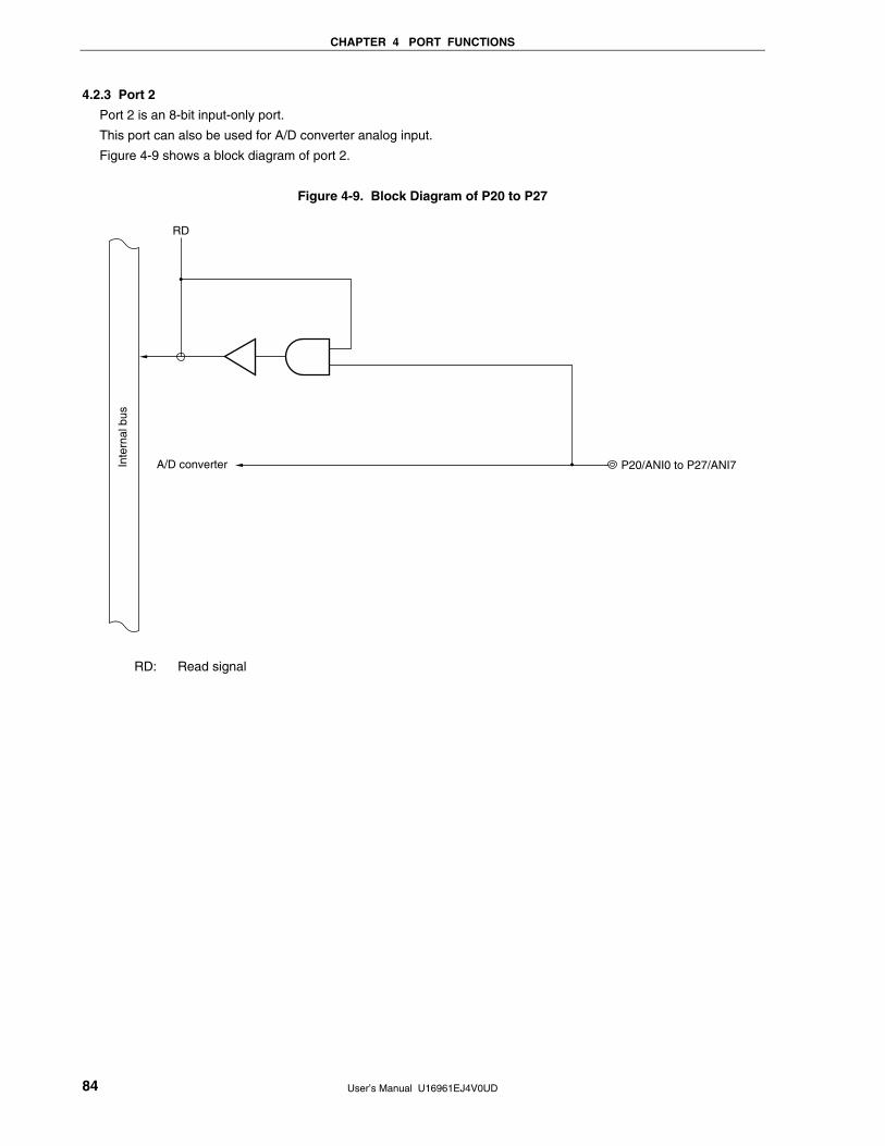
CHAPTER 4 PORT FUNCTIONS
User’s Manual U16961EJ4V0UD 84
4.2.3 Port 2
Port 2 is an 8-bit input-only port.
This port can also be used for A/D converter analog input.
Figure 4-9 shows a block diagram of port 2.
Figure 4-9. Block Diagram of P20 to P27
RD
A/D converter P20/ANI0 to P27/ANI7Inte
rnal
bus
RD: Read signal
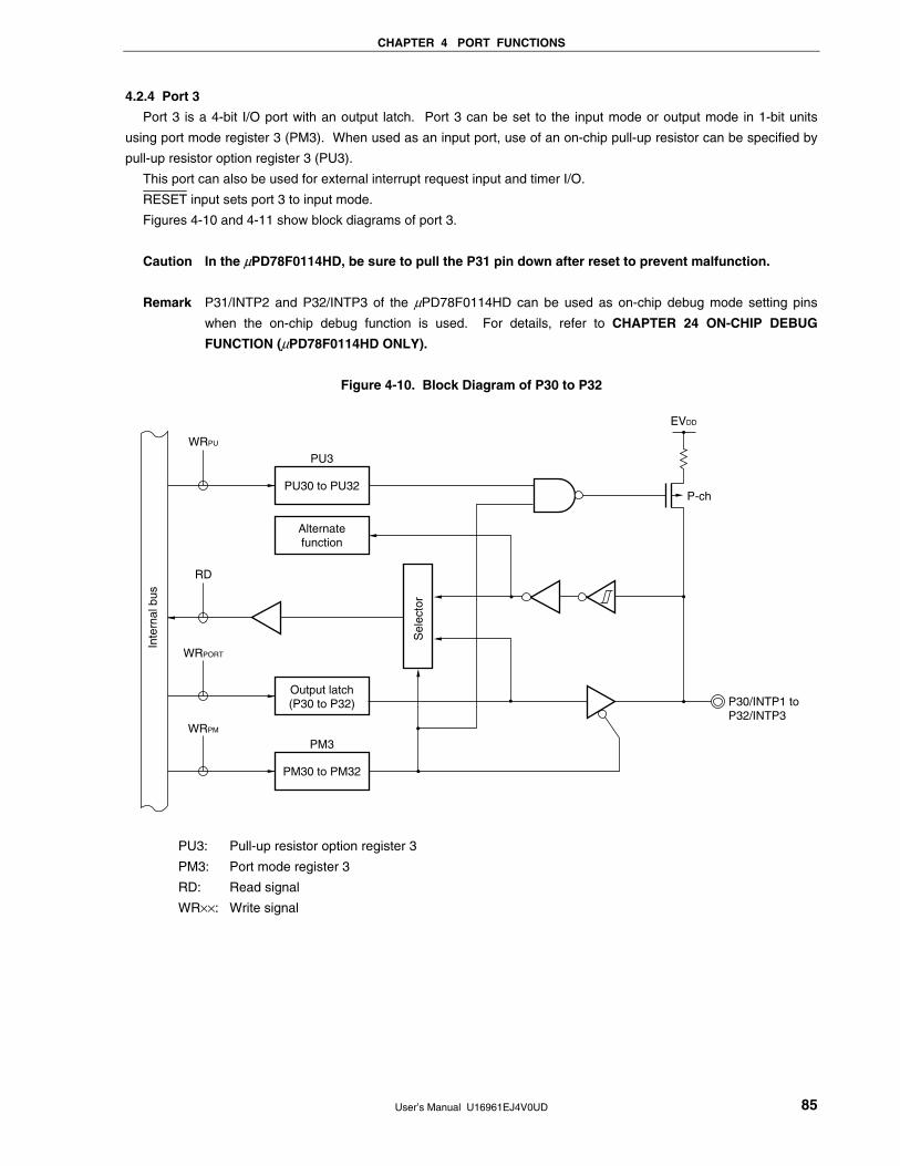
CHAPTER 4 PORT FUNCTIONS
User’s Manual U16961EJ4V0UD 85
4.2.4 Port 3
Port 3 is a 4-bit I/O port with an output latch. Port 3 can be set to the input mode or output mode in 1-bit units
using port mode register 3 (PM3). When used as an input port, use of an on-chip pull-up resistor can be specified by
pull-up resistor option register 3 (PU3).
This port can also be used for external interrupt request input and timer I/O.
RESET input sets port 3 to input mode.
Figures 4-10 and 4-11 show block diagrams of port 3.
Caution In the µPD78F0114HD, be sure to pull the P31 pin down after reset to prevent malfunction.
Remark P31/INTP2 and P32/INTP3 of the µPD78F0114HD can be used as on-chip debug mode setting pins
when the on-chip debug function is used. For details, refer to CHAPTER 24 ON-CHIP DEBUG
FUNCTION (µPD78F0114HD ONLY).
Figure 4-10. Block Diagram of P30 to P32
P30/INTP1 to P32/INTP3
WRPU
RD
WRPORT
WRPM
PU30 to PU32
Alternatefunction
Output latch(P30 to P32)
PM30 to PM32
PU3
PM3
EVDD
P-ch
Sel
ecto
r
Inte
rnal
bus
PU3: Pull-up resistor option register 3
PM3: Port mode register 3
RD: Read signal
WR××: Write signal
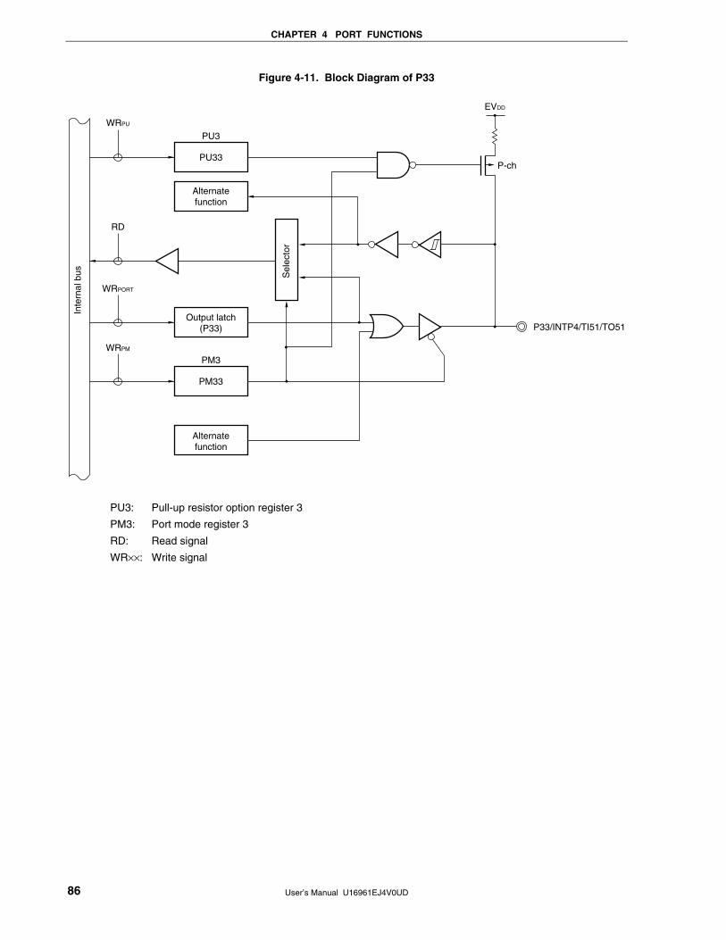
CHAPTER 4 PORT FUNCTIONS
User’s Manual U16961EJ4V0UD 86
Figure 4-11. Block Diagram of P33
P33/INTP4/TI51/TO51
WRPU
RD
WRPORT
WRPM
PU33
Alternatefunction
Output latch(P33)
PM33
PU3
PM3
Alternatefunction
EVDD
P-ch
Sel
ecto
r
Inte
rnal
bus
PU3: Pull-up resistor option register 3
PM3: Port mode register 3
RD: Read signal
WR××: Write signal
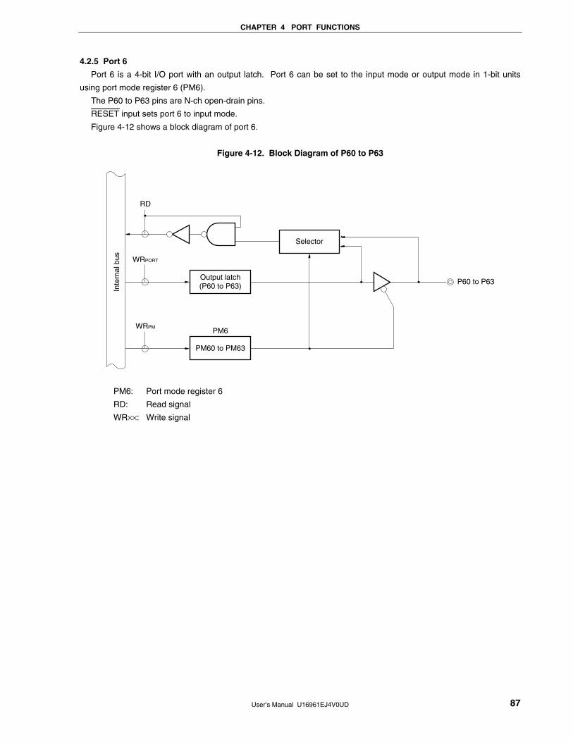
CHAPTER 4 PORT FUNCTIONS
User’s Manual U16961EJ4V0UD 87
4.2.5 Port 6
Port 6 is a 4-bit I/O port with an output latch. Port 6 can be set to the input mode or output mode in 1-bit units
using port mode register 6 (PM6).
The P60 to P63 pins are N-ch open-drain pins.
RESET input sets port 6 to input mode.
Figure 4-12 shows a block diagram of port 6.
Figure 4-12. Block Diagram of P60 to P63
RD
P60 to P63
WRPORT
WRPM
Output latch(P60 to P63)
PM60 to PM63
PM6
Selector
Inte
rnal
bus
PM6: Port mode register 6
RD: Read signal
WR××: Write signal
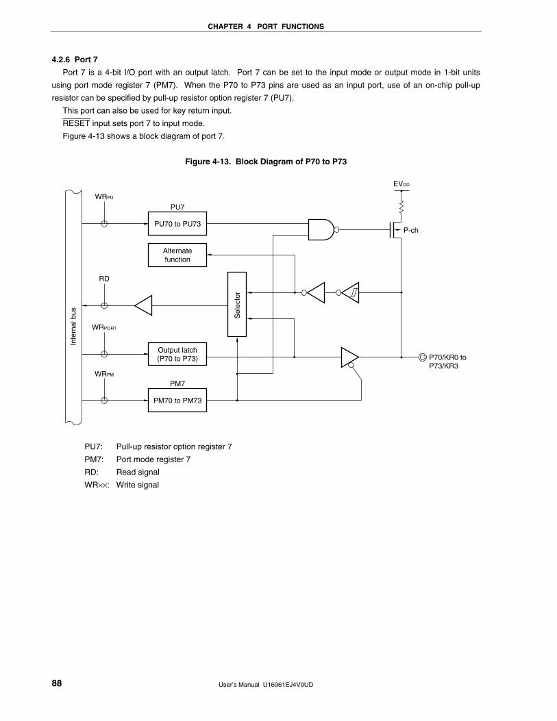
CHAPTER 4 PORT FUNCTIONS
User’s Manual U16961EJ4V0UD 88
4.2.6 Port 7
Port 7 is a 4-bit I/O port with an output latch. Port 7 can be set to the input mode or output mode in 1-bit units
using port mode register 7 (PM7). When the P70 to P73 pins are used as an input port, use of an on-chip pull-up
resistor can be specified by pull-up resistor option register 7 (PU7).
This port can also be used for key return input.
RESET input sets port 7 to input mode.
Figure 4-13 shows a block diagram of port 7.
Figure 4-13. Block Diagram of P70 to P73
P70/KR0 toP73/KR3
WRPU
RD
WRPORT
WRPM
PU70 to PU73
Alternatefunction
Output latch(P70 to P73)
PM70 to PM73
PU7
PM7
EVDD
P-chS
elec
tor
Inte
rnal
bus
PU7: Pull-up resistor option register 7
PM7: Port mode register 7
RD: Read signal
WR××: Write signal
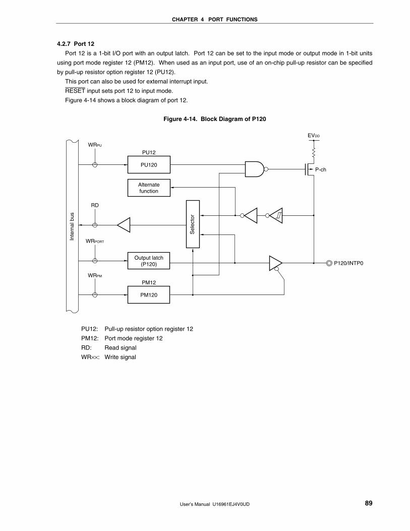
CHAPTER 4 PORT FUNCTIONS
User’s Manual U16961EJ4V0UD 89
4.2.7 Port 12
Port 12 is a 1-bit I/O port with an output latch. Port 12 can be set to the input mode or output mode in 1-bit units
using port mode register 12 (PM12). When used as an input port, use of an on-chip pull-up resistor can be specified
by pull-up resistor option register 12 (PU12).
This port can also be used for external interrupt input.
RESET input sets port 12 to input mode.
Figure 4-14 shows a block diagram of port 12.
Figure 4-14. Block Diagram of P120
P120/INTP0
WRPU
RD
WRPORT
WRPM
PU120
Alternatefunction
Output latch(P120)
PM120
PU12
PM12
EVDD
P-ch
Sel
ecto
r
Inte
rnal
bus
PU12: Pull-up resistor option register 12
PM12: Port mode register 12
RD: Read signal
WR××: Write signal
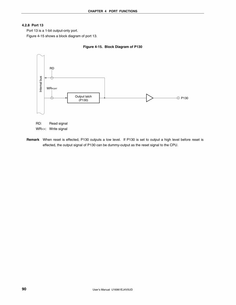
CHAPTER 4 PORT FUNCTIONS
User’s Manual U16961EJ4V0UD 90
4.2.8 Port 13
Port 13 is a 1-bit output-only port.
Figure 4-15 shows a block diagram of port 13.
Figure 4-15. Block Diagram of P130
RD
Output latch(P130)
WRPORT
P130
Inte
rnal
bus
RD: Read signal
WR××: Write signal
Remark When reset is effected, P130 outputs a low level. If P130 is set to output a high level before reset is
effected, the output signal of P130 can be dummy-output as the reset signal to the CPU.
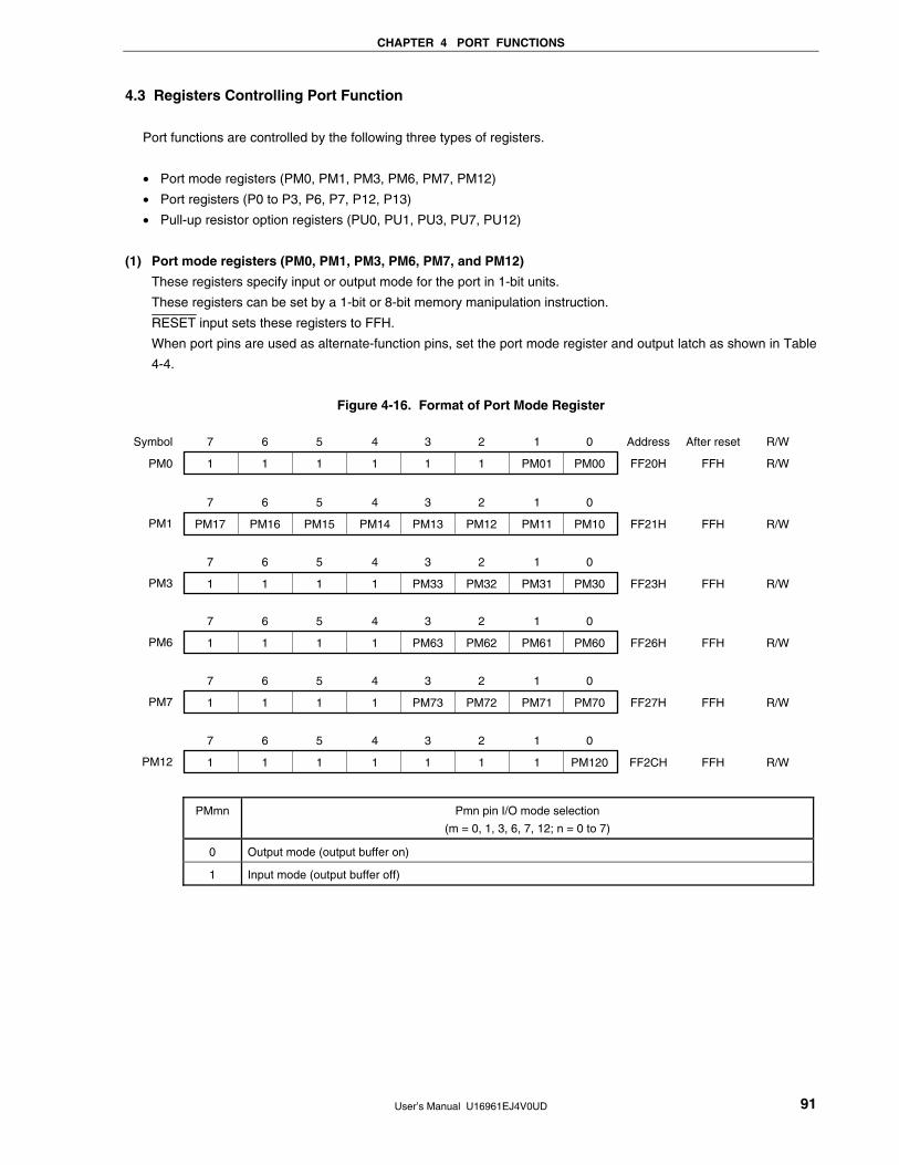
CHAPTER 4 PORT FUNCTIONS
User’s Manual U16961EJ4V0UD 91
4.3 Registers Controlling Port Function
Port functions are controlled by the following three types of registers.
• Port mode registers (PM0, PM1, PM3, PM6, PM7, PM12)
• Port registers (P0 to P3, P6, P7, P12, P13)
• Pull-up resistor option registers (PU0, PU1, PU3, PU7, PU12)
(1) Port mode registers (PM0, PM1, PM3, PM6, PM7, and PM12)
These registers specify input or output mode for the port in 1-bit units.
These registers can be set by a 1-bit or 8-bit memory manipulation instruction.
RESET input sets these registers to FFH.
When port pins are used as alternate-function pins, set the port mode register and output latch as shown in Table
4-4.
Figure 4-16. Format of Port Mode Register
7
1
Symbol
PM0
6
1
5
1
4
1
3
1
2
1
1
PM01
0
PM00
Address
FF20H
After reset
FFH
R/W
R/W
7
PM17PM1
6
PM16
5
PM15
4
PM14
3
PM13
2
PM12
1
PM11
0
PM10 FF21H FFH R/W
7
1PM3
6
1
5
1
4
1
3
PM33
2
PM32
1
PM31
0
PM30 FF23H FFH R/W
7
1PM6
6
1
5
1
4
1
3
PM63
2
PM62
1
PM61
0
PM60 FF26H FFH R/W
7
1PM7
6
1
5
1
4
1
3
PM73
2
PM72
1
PM71
0
PM70 FF27H FFH R/W
7
1PM12
6
1
5
1
4
1
3
1
2
1
1
1
0
PM120 FF2CH FFH R/W
PMmn Pmn pin I/O mode selection
(m = 0, 1, 3, 6, 7, 12; n = 0 to 7)
0 Output mode (output buffer on)
1 Input mode (output buffer off)
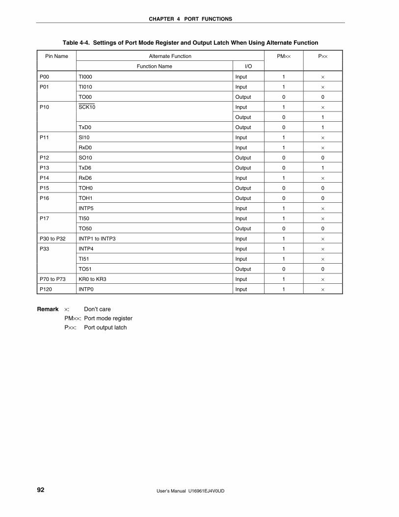
CHAPTER 4 PORT FUNCTIONS
User’s Manual U16961EJ4V0UD 92
Table 4-4. Settings of Port Mode Register and Output Latch When Using Alternate Function
Alternate Function Pin Name
Function Name I/O
PM×× P××
P00 TI000 Input 1 ×
TI010 Input 1 × P01
TO00 Output 0 0
Input 1 × SCK10
Output 0 1
P10
TxD0 Output 0 1
SI10 Input 1 × P11
RxD0 Input 1 ×
P12 SO10 Output 0 0
P13 TxD6 Output 0 1
P14 RxD6 Input 1 ×
P15 TOH0 Output 0 0
TOH1 Output 0 0 P16
INTP5 Input 1 ×
TI50 Input 1 × P17
TO50 Output 0 0
P30 to P32 INTP1 to INTP3 Input 1 ×
INTP4 Input 1 ×
TI51 Input 1 ×
P33
TO51 Output 0 0
P70 to P73 KR0 to KR3 Input 1 ×
P120 INTP0 Input 1 ×
Remark ×: Don’t care
PM××: Port mode register
P××: Port output latch
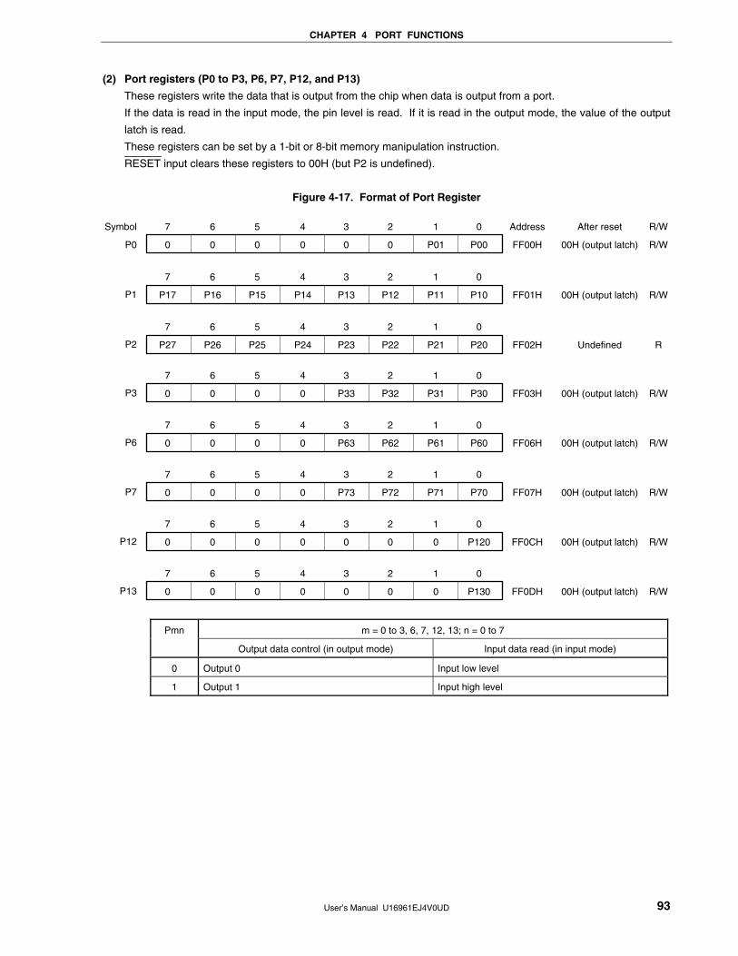
CHAPTER 4 PORT FUNCTIONS
User’s Manual U16961EJ4V0UD 93
(2) Port registers (P0 to P3, P6, P7, P12, and P13)
These registers write the data that is output from the chip when data is output from a port.
If the data is read in the input mode, the pin level is read. If it is read in the output mode, the value of the output
latch is read.
These registers can be set by a 1-bit or 8-bit memory manipulation instruction.
RESET input clears these registers to 00H (but P2 is undefined).
Figure 4-17. Format of Port Register
7
0
Symbol
P0
6
0
5
0
4
0
3
0
2
0
1
P01
0
P00
Address
FF00H
After reset
00H (output latch)
R/W
R/W
7
P17P1
6
P16
5
P15
4
P14
3
P13
2
P12
1
P11
0
P10 FF01H 00H (output latch) R/W
R
7
P27P2
6
P26
5
P25
4
P24
3
P23
2
P22
1
P21
0
P20 FF02H Undefined
7
0P3
6
0
5
0
4
0
3
P33
2
P32
1
P31
0
P30 FF03H 00H (output latch) R/W
7
0P6
6
0
5
0
4
0
3
P63
2
P62
1
P61
0
P60 FF06H 00H (output latch) R/W
7
0P7
6
0
5
0
4
0
3
P73
2
P72
1
P71
0
P70 FF07H 00H (output latch) R/W
7
0P12
6
0
5
0
4
0
3
0
2
0
1
0
0
P120 FF0CH 00H (output latch) R/W
7
0P13
6
0
5
0
4
0
3
0
2
0
1
0
0
P130 FF0DH 00H (output latch) R/W
m = 0 to 3, 6, 7, 12, 13; n = 0 to 7
Pmn
Output data control (in output mode) Input data read (in input mode)
0 Output 0 Input low level
1 Output 1 Input high level
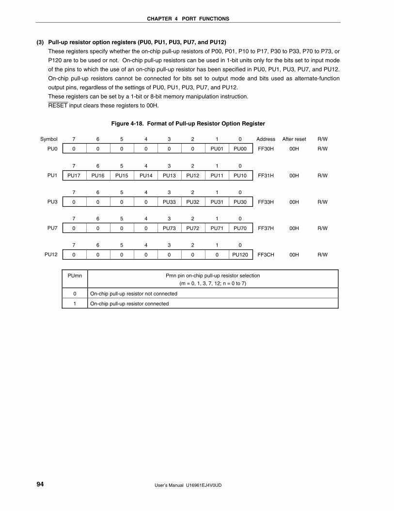
CHAPTER 4 PORT FUNCTIONS
User’s Manual U16961EJ4V0UD 94
(3) Pull-up resistor option registers (PU0, PU1, PU3, PU7, and PU12)
These registers specify whether the on-chip pull-up resistors of P00, P01, P10 to P17, P30 to P33, P70 to P73, or
P120 are to be used or not. On-chip pull-up resistors can be used in 1-bit units only for the bits set to input mode
of the pins to which the use of an on-chip pull-up resistor has been specified in PU0, PU1, PU3, PU7, and PU12.
On-chip pull-up resistors cannot be connected for bits set to output mode and bits used as alternate-function
output pins, regardless of the settings of PU0, PU1, PU3, PU7, and PU12.
These registers can be set by a 1-bit or 8-bit memory manipulation instruction.
RESET input clears these registers to 00H.
Figure 4-18. Format of Pull-up Resistor Option Register
7
0
Symbol
PU0
6
0
5
0
4
0
3
0
2
0
1
PU01
0
PU00
Address
FF30H
After reset
00H
R/W
R/W
7
PU17PU1
6
PU16
5
PU15
4
PU14
3
PU13
2
PU12
1
PU11
0
PU10 FF31H 00H R/W
7
0PU3
6
0
5
0
4
0
3
PU33
2
PU32
1
PU31
0
PU30 FF33H 00H R/W
7
0PU7
6
0
5
0
4
0
3
PU73
2
PU72
1
PU71
0
PU70 FF37H 00H R/W
7
0PU12
6
0
5
0
4
0
3
0
2
0
1
0
0
PU120 FF3CH 00H R/W
PUmn Pmn pin on-chip pull-up resistor selection
(m = 0, 1, 3, 7, 12; n = 0 to 7)
0 On-chip pull-up resistor not connected
1 On-chip pull-up resistor connected
CHAPTER 4 PORT FUNCTIONS
User’s Manual U16961EJ4V0UD 95
4.4 Port Function Operations
Port operations differ depending on whether the input or output mode is set, as shown below.
Caution In the case of a 1-bit memory manipulation instruction, although a single bit is manipulated, the
port is accessed as an 8-bit unit. Therefore, on a port with a mixture of input and output pins,
the output latch contents for pins specified as input are undefined, even for bits other than the
manipulated bit.
4.4.1 Writing to I/O port
(1) Output mode
A value is written to the output latch by a transfer instruction, and the output latch contents are output from the pin.
Once data is written to the output latch, it is retained until data is written to the output latch again.
The data of the output latch is cleared by reset.
(2) Input mode
A value is written to the output latch by a transfer instruction, but since the output buffer is off, the pin status does
not change.
Once data is written to the output latch, it is retained until data is written to the output latch again.
4.4.2 Reading from I/O port
(1) Output mode
The output latch contents are read by a transfer instruction. The output latch contents do not change.
(2) Input mode
The pin status is read by a transfer instruction. The output latch contents do not change.
4.4.3 Operations on I/O port
(1) Output mode
An operation is performed on the output latch contents, and the result is written to the output latch. The output
latch contents are output from the pins.
Once data is written to the output latch, it is retained until data is written to the output latch again.
The data of the output latch is cleared by reset.
(2) Input mode
The pin level is read and an operation is performed on its contents. The result of the operation is written to the
output latch, but since the output buffer is off, the pin status does not change.
User’s Manual U16961EJ4V0UD 96
CHAPTER 5 CLOCK GENERATOR 5.1 Functions of Clock Generator
The clock generator generates the clock to be supplied to the CPU and peripheral hardware. The following three system clock oscillators are available.
• High-speed system clock oscillator The following two high-speed system clock oscillators are available.
• Crystal/ceramic oscillator: Oscillates a clock of fXP = 2 to 16 MHz • External RC oscillator: Oscillates a clock of fXP = 3 to 4 MHz
High-speed system clock oscillation can be selected using the option byte. Refer to CHAPTER 22 OPTION
BYTE for details. The high-speed system clock oscillator can be stopped by executing the STOP instruction or setting the main
OSC control register (MOC) and processor clock control register (PCC). • Internal oscillator The Internal oscillator oscillates a clock of fR = 240 kHz (TYP.). Oscillation can be stopped by setting the
internal oscillation mode register (RCM) when “can be stopped by software” is set by the option byte and the high-speed system clock is used as the CPU clock.
• Subsystem clock oscillator The subsystem clock oscillator oscillates a clock of fXT = 32.768 kHz. Oscillation cannot be stopped. When
subsystem clock oscillator is not used, setting not to use the on-chip feedback resistor is possible using the processor clock control register (PCC), and the operating current can be reduced in the STOP mode.
Remarks 1. fXP: High-speed system clock oscillation frequency 2. fR: Internal oscillation clock oscillation frequency 3. fXT: Subsystem clock oscillation frequency
5.2 Configuration of Clock Generator
The clock generator includes the following hardware.
Table 5-1. Configuration of Clock Generator
Item Configuration
Control registers Processor clock control register (PCC) Internal oscillation mode register (RCM) Main clock mode register (MCM) Main OSC control register (MOC) Oscillation stabilization time counter status register (OSTC) Oscillation stabilization time select register (OSTS)
Oscillators High-speed system clock oscillator Internal oscillator Subsystem clock oscillator
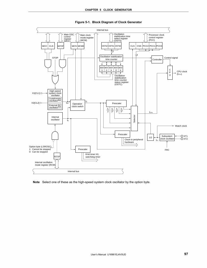
CHAPTER 5 CLOCK GENERATOR
User’s Manual U16961EJ4V0UD 97
Figure 5-1. Block Diagram of Clock Generator
fXP
fXT
FRC
XT1XT2
fX22
STOP
MSTOP
fX23
fX24
fX2
4
RSTOP
CSS PCC2CLSMCM0MCSCLSMCC OSTS1 OSTS0OSTS2
1/2
3
MOST16
MOST15
MOST14
MOST13
MOST11 C
PU
fR
fX
PCC1 PCC0
Internal bus
Internal oscillation mode register (RCM)
Main OSC control register(MOC)
Internal bus
Internaloscillator
Option byte (LSROSC)1: Cannot be stopped0: Can be stopped
CPU clock(fCPU)
Controller
Processor clock control register (PCC)
Main clock mode register(MCM)
Oscillation stabilization time counter
Oscillation stabilization time select register (OSTS)
Clock to peripheral hardware
PrescalerOperation clock switch
8-bit timer H1, watchdog timer
Prescaler
PrescalerS
elec
tor
Subsystem clock oscillator
Watch clock
fCPU
Control signal
X1[CL1]
X2[CL2]
High-speed system clock
oscillator
Crystal/ceramicoscillatorNote
External RCoscillatorNote
Oscillation stabilization time counter status register (OSTC)
Note Select one of these as the high-speed system clock oscillator by the option byte.
CHAPTER 5 CLOCK GENERATOR
User’s Manual U16961EJ4V0UD 98
5.3 Registers Controlling Clock Generator
The following six registers are used to control the clock generator. • Processor clock control register (PCC) • Internal oscillation mode register (RCM) • Main clock mode register (MCM) • Main OSC control register (MOC) • Oscillation stabilization time counter status register (OSTC) • Oscillation stabilization time select register (OSTS)
(1) Processor clock control register (PCC)
The PCC register is used to select the CPU clock, the division ratio, main system clock oscillator operation/stop and whether to use the on-chip feedback resistorNote of the subsystem clock oscillator. PCC can be set by a 1-bit or 8-bit memory manipulation instruction. RESET input clears PCC to 00H.
Note The feedback resistor is required to control the bias point of the oscillation waveform so that the bias point
is in the middle of the power supply voltage (see Figure 5-13 Subsystem Clock Feedback Resistor).
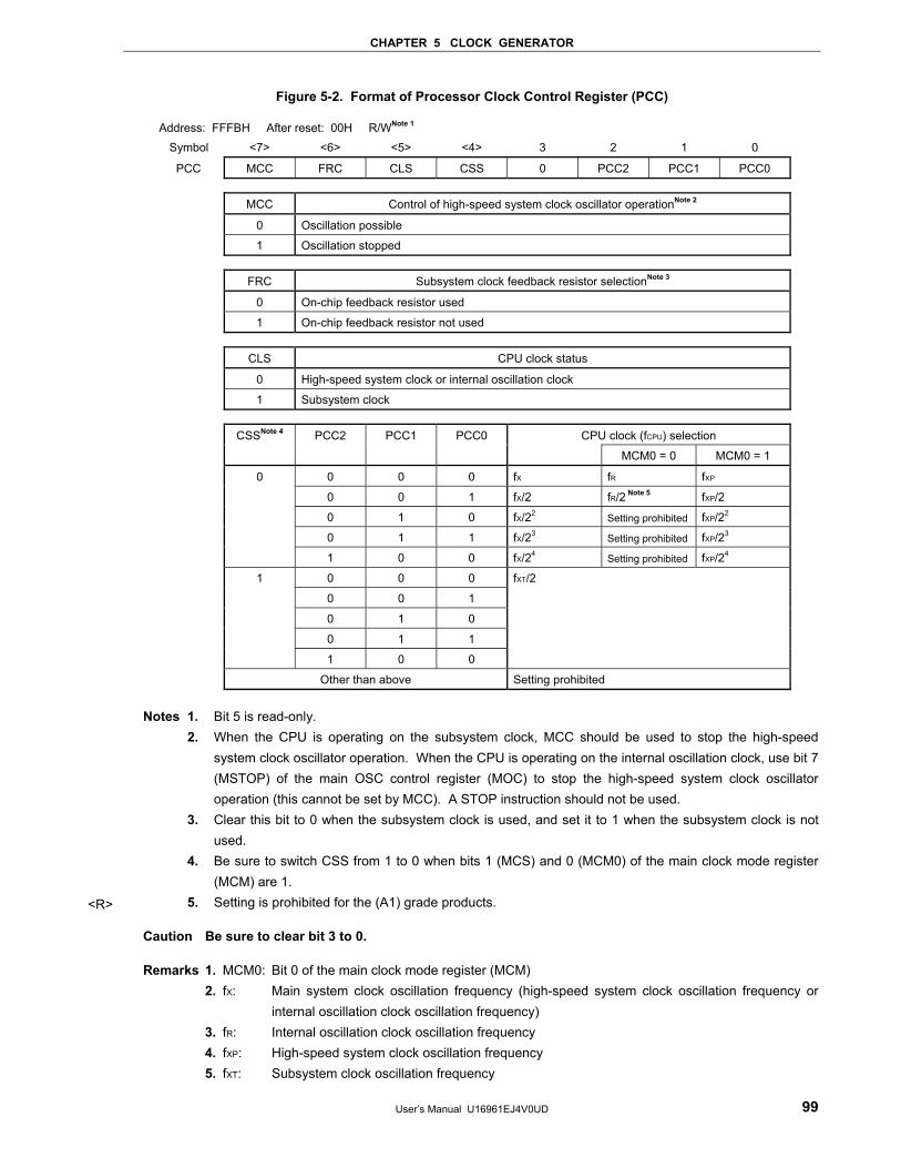
CHAPTER 5 CLOCK GENERATOR
User’s Manual U16961EJ4V0UD 99
Figure 5-2. Format of Processor Clock Control Register (PCC)
Address: FFFBH After reset: 00H R/WNote 1 Symbol <7> <6> <5> <4> 3 2 1 0
PCC MCC FRC CLS CSS 0 PCC2 PCC1 PCC0
MCC Control of high-speed system clock oscillator operationNote 2
0 Oscillation possible
1 Oscillation stopped
FRC Subsystem clock feedback resistor selectionNote 3
0 On-chip feedback resistor used
1 On-chip feedback resistor not used
CLS CPU clock status
0 High-speed system clock or internal oscillation clock
1 Subsystem clock
CPU clock (fCPU) selection
CSSNote 4 PCC2 PCC1 PCC0
MCM0 = 0 MCM0 = 1
0 0 0 fX fR fXP
0 0 1 fX/2 fR/2 Note 5 fXP/2
0 1 0 fX/22 Setting prohibited fXP/22
0 1 1 fX/23 Setting prohibited fXP/23
0
1 0 0 fX/24 Setting prohibited fXP/24
0 0 0
0 0 1
0 1 0
0 1 1
1
1 0 0
fXT/2
Other than above Setting prohibited
Notes 1. Bit 5 is read-only. 2. When the CPU is operating on the subsystem clock, MCC should be used to stop the high-speed
system clock oscillator operation. When the CPU is operating on the internal oscillation clock, use bit 7 (MSTOP) of the main OSC control register (MOC) to stop the high-speed system clock oscillator operation (this cannot be set by MCC). A STOP instruction should not be used.
3. Clear this bit to 0 when the subsystem clock is used, and set it to 1 when the subsystem clock is not used.
4. Be sure to switch CSS from 1 to 0 when bits 1 (MCS) and 0 (MCM0) of the main clock mode register (MCM) are 1.
5. Setting is prohibited for the (A1) grade products.
Caution Be sure to clear bit 3 to 0.
Remarks 1. MCM0: Bit 0 of the main clock mode register (MCM) 2. fX: Main system clock oscillation frequency (high-speed system clock oscillation frequency or
internal oscillation clock oscillation frequency) 3. fR: Internal oscillation clock oscillation frequency 4. fXP: High-speed system clock oscillation frequency 5. fXT: Subsystem clock oscillation frequency
<R>
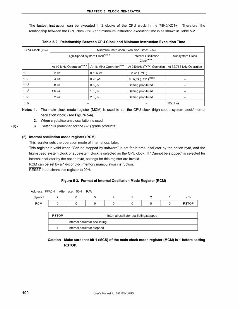
CHAPTER 5 CLOCK GENERATOR
User’s Manual U16961EJ4V0UD 100
The fastest instruction can be executed in 2 clocks of the CPU clock in the 78K0/KC1+. Therefore, the relationship between the CPU clock (fCPU) and minimum instruction execution time is as shown in Table 5-2.
Table 5-2. Relationship Between CPU Clock and Minimum Instruction Execution Time
Minimum Instruction Execution Time: 2/fCPU
High-Speed System ClockNote 1 Internal Oscillation ClockNote 1
Subsystem Clock
CPU Clock (fCPU)
At 10 MHz OperationNote 2 At 16 MHz OperationNote 2 At 240 kHz (TYP.) Operation At 32.768 kHz Operation
fX 0.2 μs 0.125 μs 8.3 μs (TYP.) −
fX/2 0.4 μs 0.25 μs 16.6 μs (TYP.) Note 3 −
fX/22 0.8 μs 0.5 μs Setting prohibited −
fX/23 1.6 μs 1.0 μs Setting prohibited −
fX/24 3.2 μs 2.0 μs Setting prohibited −
fXT/2 − − 122.1 μs
Notes 1. The main clock mode register (MCM) is used to set the CPU clock (high-speed system clock/internal oscillation clock) (see Figure 5-4).
2. When crystal/ceramic oscillation is used 3. Setting is prohibited for the (A1) grade products. (2) Internal oscillation mode register (RCM)
This register sets the operation mode of internal oscillator. This register is valid when “Can be stopped by software” is set for internal oscillator by the option byte, and the high-speed system clock or subsystem clock is selected as the CPU clock. If “Cannot be stopped” is selected for internal oscillator by the option byte, settings for this register are invalid. RCM can be set by a 1-bit or 8-bit memory manipulation instruction. RESET input clears this register to 00H.
Figure 5-3. Format of Internal Oscillation Mode Register (RCM)
Address: FFA0H After reset: 00H R/W
Symbol 7 6 5 4 3 2 1 <0>
RCM 0 0 0 0 0 0 0 RSTOP
RSTOP Internal oscillator oscillating/stopped
0 Internal oscillator oscillating
1 Internal oscillator stopped
Caution Make sure that bit 1 (MCS) of the main clock mode register (MCM) is 1 before setting
RSTOP.
<R>
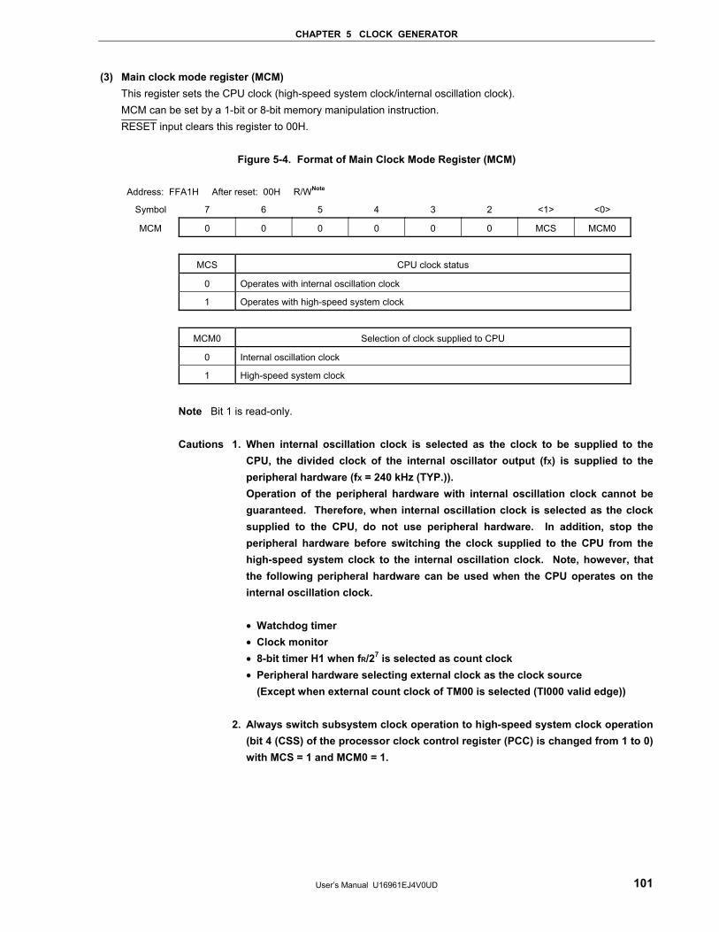
CHAPTER 5 CLOCK GENERATOR
User’s Manual U16961EJ4V0UD 101
(3) Main clock mode register (MCM) This register sets the CPU clock (high-speed system clock/internal oscillation clock). MCM can be set by a 1-bit or 8-bit memory manipulation instruction. RESET input clears this register to 00H.
Figure 5-4. Format of Main Clock Mode Register (MCM)
Address: FFA1H After reset: 00H R/WNote
Symbol 7 6 5 4 3 2 <1> <0>
MCM 0 0 0 0 0 0 MCS MCM0
MCS CPU clock status
0 Operates with internal oscillation clock
1 Operates with high-speed system clock
MCM0 Selection of clock supplied to CPU
0 Internal oscillation clock
1 High-speed system clock
Note Bit 1 is read-only.
Cautions 1. When internal oscillation clock is selected as the clock to be supplied to the
CPU, the divided clock of the internal oscillator output (fX) is supplied to the peripheral hardware (fX = 240 kHz (TYP.)).
Operation of the peripheral hardware with internal oscillation clock cannot be guaranteed. Therefore, when internal oscillation clock is selected as the clock supplied to the CPU, do not use peripheral hardware. In addition, stop the peripheral hardware before switching the clock supplied to the CPU from the high-speed system clock to the internal oscillation clock. Note, however, that the following peripheral hardware can be used when the CPU operates on the internal oscillation clock.
• Watchdog timer • Clock monitor • 8-bit timer H1 when fR/27 is selected as count clock • Peripheral hardware selecting external clock as the clock source (Except when external count clock of TM00 is selected (TI000 valid edge)) 2. Always switch subsystem clock operation to high-speed system clock operation
(bit 4 (CSS) of the processor clock control register (PCC) is changed from 1 to 0) with MCS = 1 and MCM0 = 1.
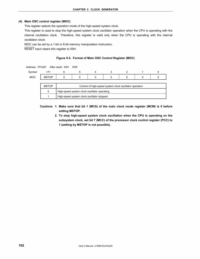
CHAPTER 5 CLOCK GENERATOR
User’s Manual U16961EJ4V0UD 102
(4) Main OSC control register (MOC) This register selects the operation mode of the high-speed system clock. This register is used to stop the high-speed system clock oscillator operation when the CPU is operating with the internal oscillation clock. Therefore, this register is valid only when the CPU is operating with the internal oscillation clock. MOC can be set by a 1-bit or 8-bit memory manipulation instruction. RESET input clears this register to 00H.
Figure 5-5. Format of Main OSC Control Register (MOC)
Address: FFA2H After reset: 00H R/W
Symbol <7> 6 5 4 3 2 1 0
MOC MSTOP 0 0 0 0 0 0 0
MSTOP Control of high-speed system clock oscillator operation
0 High-speed system clock oscillator operating
1 High-speed system clock oscillator stopped
Cautions 1. Make sure that bit 1 (MCS) of the main clock mode register (MCM) is 0 before
setting MSTOP. 2. To stop high-speed system clock oscillation when the CPU is operating on the
subsystem clock, set bit 7 (MCC) of the processor clock control register (PCC) to 1 (setting by MSTOP is not possible).
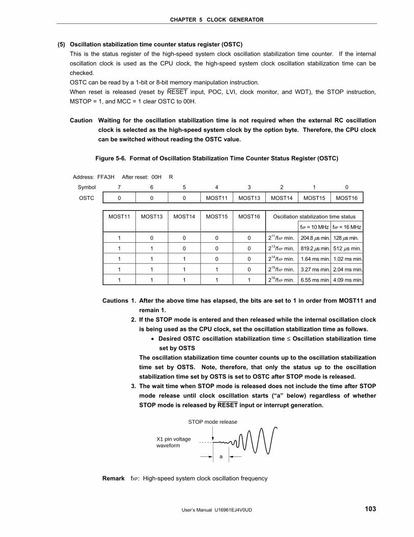
CHAPTER 5 CLOCK GENERATOR
User’s Manual U16961EJ4V0UD 103
(5) Oscillation stabilization time counter status register (OSTC) This is the status register of the high-speed system clock oscillation stabilization time counter. If the internal oscillation clock is used as the CPU clock, the high-speed system clock oscillation stabilization time can be checked. OSTC can be read by a 1-bit or 8-bit memory manipulation instruction. When reset is released (reset by RESET input, POC, LVI, clock monitor, and WDT), the STOP instruction, MSTOP = 1, and MCC = 1 clear OSTC to 00H.
Caution Waiting for the oscillation stabilization time is not required when the external RC oscillation
clock is selected as the high-speed system clock by the option byte. Therefore, the CPU clock can be switched without reading the OSTC value.
Figure 5-6. Format of Oscillation Stabilization Time Counter Status Register (OSTC)
Address: FFA3H After reset: 00H R
Symbol 7 6 5 4 3 2 1 0
OSTC 0 0 0 MOST11 MOST13 MOST14 MOST15 MOST16
MOST13 MOST14 MOST15 MOST16 Oscillation stabilization time status
MOST11
fXP = 10 MHz fXP = 16 MHz
1 0 0 0 0 211/fXP min. 204.8 μs min. 128 μs min.
1 1 0 0 0 213/fXP min. 819.2 μs min. 512 μs min.
1 1 1 0 0 214/fXP min. 1.64 ms min. 1.02 ms min.
1 1 1 1 0 215/fXP min. 3.27 ms min. 2.04 ms min.
1 1 1 1 1 216/fXP min. 6.55 ms min. 4.09 ms min.
Cautions 1. After the above time has elapsed, the bits are set to 1 in order from MOST11 and
remain 1. 2. If the STOP mode is entered and then released while the internal oscillation clock
is being used as the CPU clock, set the oscillation stabilization time as follows. • Desired OSTC oscillation stabilization time ≤ Oscillation stabilization time
set by OSTS The oscillation stabilization time counter counts up to the oscillation stabilization
time set by OSTS. Note, therefore, that only the status up to the oscillation stabilization time set by OSTS is set to OSTC after STOP mode is released.
3. The wait time when STOP mode is released does not include the time after STOP mode release until clock oscillation starts (“a” below) regardless of whether STOP mode is released by RESET input or interrupt generation.
STOP mode release
X1 pin voltage waveform
a
Remark fXP: High-speed system clock oscillation frequency
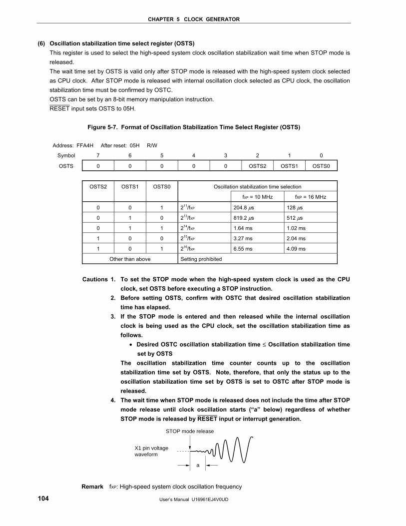
CHAPTER 5 CLOCK GENERATOR
User’s Manual U16961EJ4V0UD 104
(6) Oscillation stabilization time select register (OSTS) This register is used to select the high-speed system clock oscillation stabilization wait time when STOP mode is released. The wait time set by OSTS is valid only after STOP mode is released with the high-speed system clock selected as CPU clock. After STOP mode is released with internal oscillation clock selected as CPU clock, the oscillation stabilization time must be confirmed by OSTC. OSTS can be set by an 8-bit memory manipulation instruction. RESET input sets OSTS to 05H.
Figure 5-7. Format of Oscillation Stabilization Time Select Register (OSTS)
Address: FFA4H After reset: 05H R/W
Symbol 7 6 5 4 3 2 1 0
OSTS 0 0 0 0 0 OSTS2 OSTS1 OSTS0
OSTS2 OSTS1 OSTS0 Oscillation stabilization time selection
fXP = 10 MHz fXP = 16 MHz
0 0 1 211/fXP 204.8 μs 128 μs
0 1 0 213/fXP 819.2 μs 512 μs
0 1 1 214/fXP 1.64 ms 1.02 ms
1 0 0 215/fXP 3.27 ms 2.04 ms
1 0 1 216/fXP 6.55 ms 4.09 ms
Other than above Setting prohibited
Cautions 1. To set the STOP mode when the high-speed system clock is used as the CPU
clock, set OSTS before executing a STOP instruction. 2. Before setting OSTS, confirm with OSTC that desired oscillation stabilization
time has elapsed. 3. If the STOP mode is entered and then released while the internal oscillation
clock is being used as the CPU clock, set the oscillation stabilization time as follows.
• Desired OSTC oscillation stabilization time ≤ Oscillation stabilization time set by OSTS
The oscillation stabilization time counter counts up to the oscillation stabilization time set by OSTS. Note, therefore, that only the status up to the oscillation stabilization time set by OSTS is set to OSTC after STOP mode is released.
4. The wait time when STOP mode is released does not include the time after STOP mode release until clock oscillation starts (“a” below) regardless of whether STOP mode is released by RESET input or interrupt generation.
STOP mode release
X1 pin voltage waveform
a
Remark fXP: High-speed system clock oscillation frequency
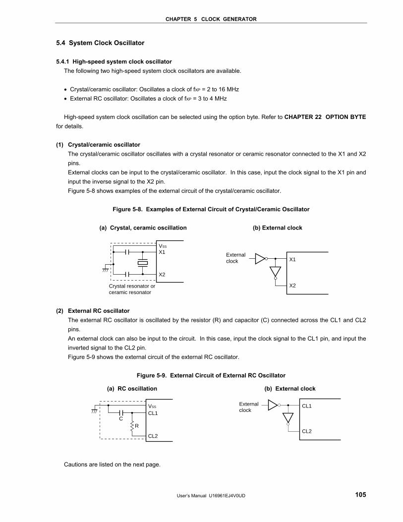
CHAPTER 5 CLOCK GENERATOR
User’s Manual U16961EJ4V0UD 105
5.4 System Clock Oscillator 5.4.1 High-speed system clock oscillator
The following two high-speed system clock oscillators are available. • Crystal/ceramic oscillator: Oscillates a clock of fXP = 2 to 16 MHz • External RC oscillator: Oscillates a clock of fXP = 3 to 4 MHz High-speed system clock oscillation can be selected using the option byte. Refer to CHAPTER 22 OPTION BYTE
for details. (1) Crystal/ceramic oscillator
The crystal/ceramic oscillator oscillates with a crystal resonator or ceramic resonator connected to the X1 and X2 pins. External clocks can be input to the crystal/ceramic oscillator. In this case, input the clock signal to the X1 pin and input the inverse signal to the X2 pin. Figure 5-8 shows examples of the external circuit of the crystal/ceramic oscillator.
Figure 5-8. Examples of External Circuit of Crystal/Ceramic Oscillator
(a) Crystal, ceramic oscillation (b) External clock
VSS
X1
X2
Crystal resonator or ceramic resonator
Externalclock X1
X2
(2) External RC oscillator
The external RC oscillator is oscillated by the resistor (R) and capacitor (C) connected across the CL1 and CL2 pins. An external clock can also be input to the circuit. In this case, input the clock signal to the CL1 pin, and input the inverted signal to the CL2 pin. Figure 5-9 shows the external circuit of the external RC oscillator.
Figure 5-9. External Circuit of External RC Oscillator
(a) RC oscillation (b) External clock
VSS
CL1
CL2
RC
Externalclock
CL1
CL2
Cautions are listed on the next page.
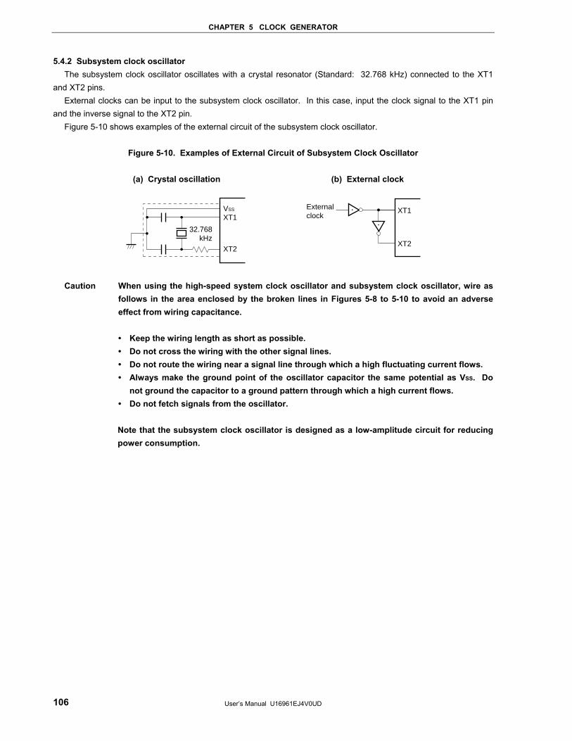
CHAPTER 5 CLOCK GENERATOR
User’s Manual U16961EJ4V0UD 106
5.4.2 Subsystem clock oscillator The subsystem clock oscillator oscillates with a crystal resonator (Standard: 32.768 kHz) connected to the XT1
and XT2 pins. External clocks can be input to the subsystem clock oscillator. In this case, input the clock signal to the XT1 pin
and the inverse signal to the XT2 pin. Figure 5-10 shows examples of the external circuit of the subsystem clock oscillator.
Figure 5-10. Examples of External Circuit of Subsystem Clock Oscillator
(a) Crystal oscillation (b) External clock
XT1
XT2
Externalclock
XT2
VSS
XT1
32.768kHz
Caution When using the high-speed system clock oscillator and subsystem clock oscillator, wire as follows in the area enclosed by the broken lines in Figures 5-8 to 5-10 to avoid an adverse effect from wiring capacitance.
• Keep the wiring length as short as possible. • Do not cross the wiring with the other signal lines. • Do not route the wiring near a signal line through which a high fluctuating current flows. • Always make the ground point of the oscillator capacitor the same potential as VSS. Do
not ground the capacitor to a ground pattern through which a high current flows. • Do not fetch signals from the oscillator. Note that the subsystem clock oscillator is designed as a low-amplitude circuit for reducing power consumption.
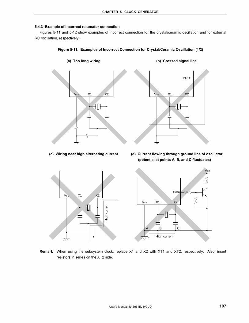
CHAPTER 5 CLOCK GENERATOR
User’s Manual U16961EJ4V0UD 107
5.4.3 Example of incorrect resonator connection Figures 5-11 and 5-12 show examples of incorrect connection for the crystal/ceramic oscillation and for external
RC oscillation, respectively.
Figure 5-11. Examples of Incorrect Connection for Crystal/Ceramic Oscillation (1/2) (a) Too long wiring (b) Crossed signal line
X2VSS X1 X1VSS X2
PORT
(c) Wiring near high alternating current (d) Current flowing through ground line of oscillator (potential at points A, B, and C fluctuates)
VSS X1 X2
VSS X1 X2
A B C
Pmn
VDD
High current
Hig
h cu
rren
t
Remark When using the subsystem clock, replace X1 and X2 with XT1 and XT2, respectively. Also, insert resistors in series on the XT2 side.
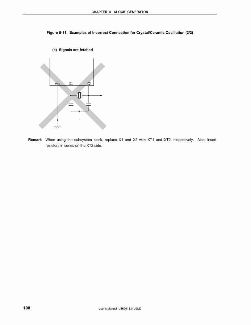
CHAPTER 5 CLOCK GENERATOR
User’s Manual U16961EJ4V0UD 108
Figure 5-11. Examples of Incorrect Connection for Crystal/Ceramic Oscillation (2/2)
(e) Signals are fetched
VSS X1 X2
Remark When using the subsystem clock, replace X1 and X2 with XT1 and XT2, respectively. Also, insert resistors in series on the XT2 side.
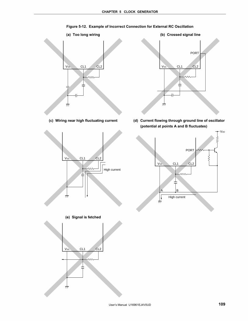
CHAPTER 5 CLOCK GENERATOR
User’s Manual U16961EJ4V0UD 109
Figure 5-12. Example of Incorrect Connection for External RC Oscillation
(a) Too long wiring (b) Crossed signal line
CL2CL1VSS
CL2
PORT
CL1VSS
(c) Wiring near high fluctuating current (d) Current flowing through ground line of oscillator (potential at points A and B fluctuates)
CL2CL1VSS
High current
VSS
VDD
CL1 CL2
BA
PORT
High current
(e) Signal is fetched
CL2CL1VSS
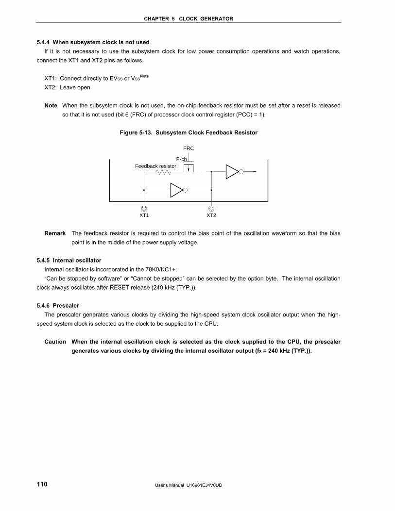
CHAPTER 5 CLOCK GENERATOR
User’s Manual U16961EJ4V0UD 110
5.4.4 When subsystem clock is not used If it is not necessary to use the subsystem clock for low power consumption operations and watch operations,
connect the XT1 and XT2 pins as follows. XT1: Connect directly to EVSS or VSS
Note XT2: Leave open Note When the subsystem clock is not used, the on-chip feedback resistor must be set after a reset is released
so that it is not used (bit 6 (FRC) of processor clock control register (PCC) = 1).
Figure 5-13. Subsystem Clock Feedback Resistor
FRC
P-chFeedback resistor
XT1 XT2
Remark The feedback resistor is required to control the bias point of the oscillation waveform so that the bias point is in the middle of the power supply voltage.
5.4.5 Internal oscillator
Internal oscillator is incorporated in the 78K0/KC1+. “Can be stopped by software” or “Cannot be stopped” can be selected by the option byte. The internal oscillation
clock always oscillates after RESET release (240 kHz (TYP.)). 5.4.6 Prescaler
The prescaler generates various clocks by dividing the high-speed system clock oscillator output when the high-speed system clock is selected as the clock to be supplied to the CPU.
Caution When the internal oscillation clock is selected as the clock supplied to the CPU, the prescaler generates various clocks by dividing the internal oscillator output (fX = 240 kHz (TYP.)).
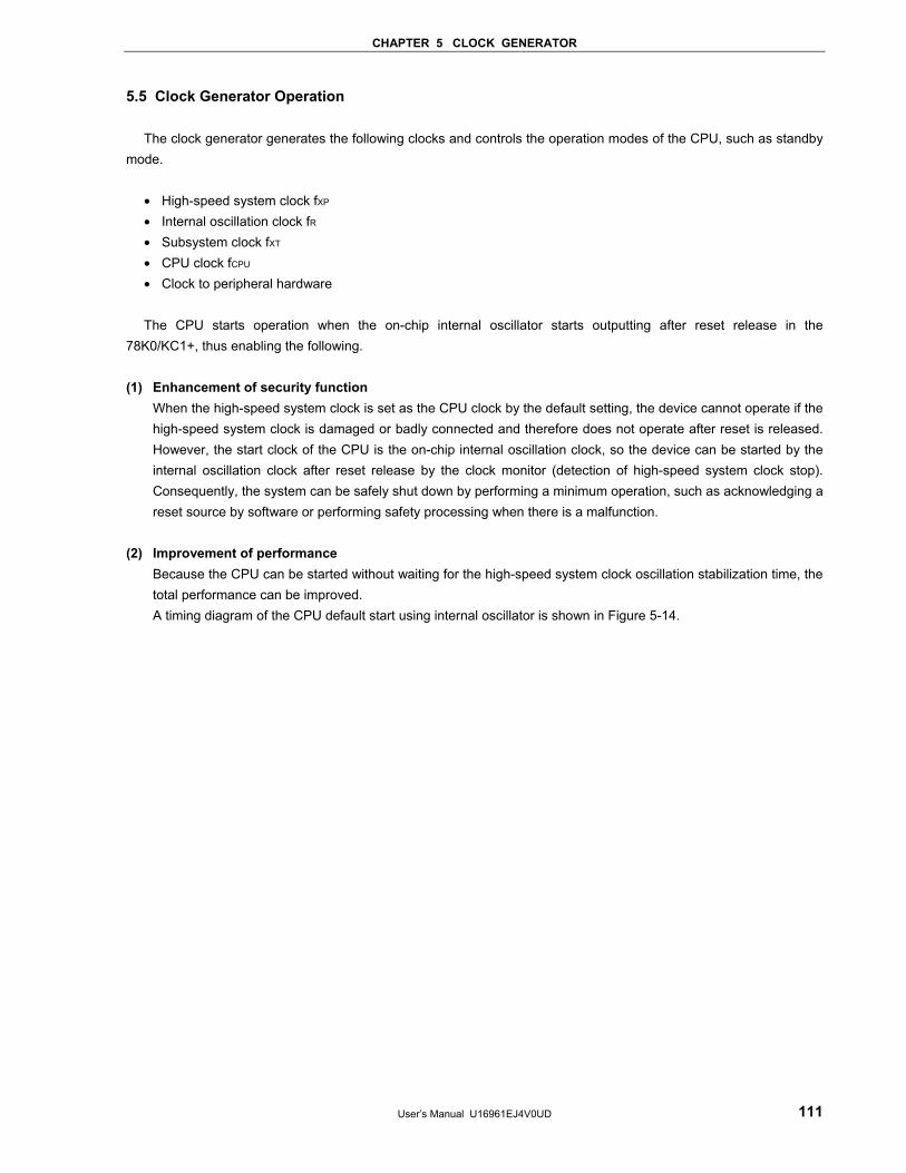
CHAPTER 5 CLOCK GENERATOR
User’s Manual U16961EJ4V0UD 111
5.5 Clock Generator Operation
The clock generator generates the following clocks and controls the operation modes of the CPU, such as standby mode.
• High-speed system clock fXP • Internal oscillation clock fR • Subsystem clock fXT • CPU clock fCPU • Clock to peripheral hardware The CPU starts operation when the on-chip internal oscillator starts outputting after reset release in the
78K0/KC1+, thus enabling the following. (1) Enhancement of security function
When the high-speed system clock is set as the CPU clock by the default setting, the device cannot operate if the high-speed system clock is damaged or badly connected and therefore does not operate after reset is released. However, the start clock of the CPU is the on-chip internal oscillation clock, so the device can be started by the internal oscillation clock after reset release by the clock monitor (detection of high-speed system clock stop). Consequently, the system can be safely shut down by performing a minimum operation, such as acknowledging a reset source by software or performing safety processing when there is a malfunction.
(2) Improvement of performance
Because the CPU can be started without waiting for the high-speed system clock oscillation stabilization time, the total performance can be improved. A timing diagram of the CPU default start using internal oscillator is shown in Figure 5-14.
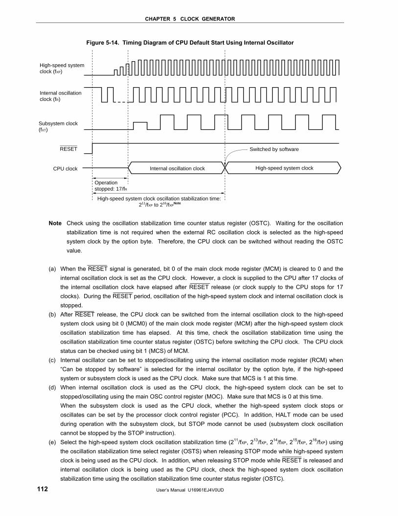
CHAPTER 5 CLOCK GENERATOR
User’s Manual U16961EJ4V0UD 112
Figure 5-14. Timing Diagram of CPU Default Start Using Internal Oscillator
Internal oscillation clock (fR)
CPU clock
High-speed system clock (fXP)
Operation stopped: 17/fR
High-speed system clock oscillation stabilization time: 211/fXP to 216/fXP
Note
RESET
Internal oscillation clock High-speed system clock
Switched by software
Subsystem clock(fXT)
Note Check using the oscillation stabilization time counter status register (OSTC). Waiting for the oscillation stabilization time is not required when the external RC oscillation clock is selected as the high-speed system clock by the option byte. Therefore, the CPU clock can be switched without reading the OSTC value.
(a) When the RESET signal is generated, bit 0 of the main clock mode register (MCM) is cleared to 0 and the
internal oscillation clock is set as the CPU clock. However, a clock is supplied to the CPU after 17 clocks of the internal oscillation clock have elapsed after RESET release (or clock supply to the CPU stops for 17 clocks). During the RESET period, oscillation of the high-speed system clock and internal oscillation clock is stopped.
(b) After RESET release, the CPU clock can be switched from the internal oscillation clock to the high-speed system clock using bit 0 (MCM0) of the main clock mode register (MCM) after the high-speed system clock oscillation stabilization time has elapsed. At this time, check the oscillation stabilization time using the oscillation stabilization time counter status register (OSTC) before switching the CPU clock. The CPU clock status can be checked using bit 1 (MCS) of MCM.
(c) Internal oscillator can be set to stopped/oscillating using the internal oscillation mode register (RCM) when “Can be stopped by software” is selected for the internal oscillator by the option byte, if the high-speed system or subsystem clock is used as the CPU clock. Make sure that MCS is 1 at this time.
(d) When internal oscillation clock is used as the CPU clock, the high-speed system clock can be set to stopped/oscillating using the main OSC control register (MOC). Make sure that MCS is 0 at this time.
When the subsystem clock is used as the CPU clock, whether the high-speed system clock stops or oscillates can be set by the processor clock control register (PCC). In addition, HALT mode can be used during operation with the subsystem clock, but STOP mode cannot be used (subsystem clock oscillation cannot be stopped by the STOP instruction).
(e) Select the high-speed system clock oscillation stabilization time (211/fXP, 213/fXP, 214/fXP, 215/fXP, 216/fXP) using the oscillation stabilization time select register (OSTS) when releasing STOP mode while high-speed system clock is being used as the CPU clock. In addition, when releasing STOP mode while RESET is released and internal oscillation clock is being used as the CPU clock, check the high-speed system clock oscillation stabilization time using the oscillation stabilization time counter status register (OSTC).
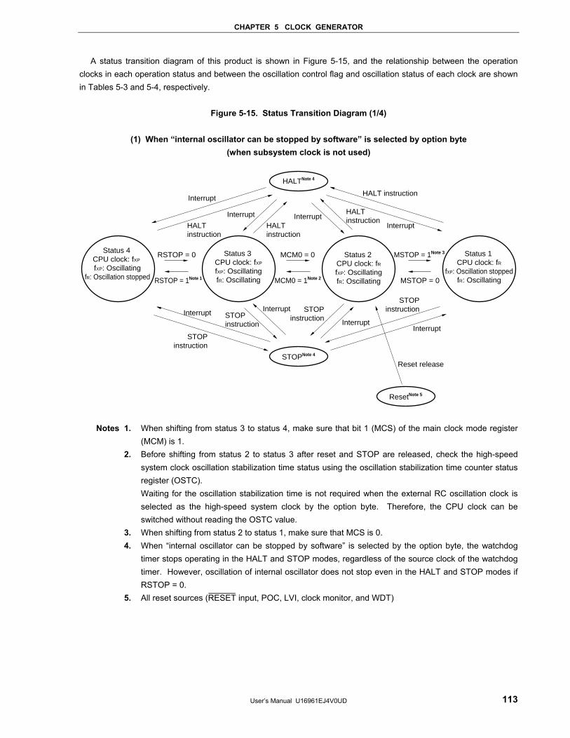
CHAPTER 5 CLOCK GENERATOR
User’s Manual U16961EJ4V0UD 113
A status transition diagram of this product is shown in Figure 5-15, and the relationship between the operation clocks in each operation status and between the oscillation control flag and oscillation status of each clock are shown in Tables 5-3 and 5-4, respectively.
Figure 5-15. Status Transition Diagram (1/4)
(1) When “internal oscillator can be stopped by software” is selected by option byte (when subsystem clock is not used)
Status 4CPU clock: fXP fXP: Oscillating
fR: Oscillation stopped
Status 3CPU clock: fXP
fXP: OscillatingfR: Oscillating
Status 1CPU clock: fR
fXP: Oscillation stoppedfR: Oscillating
Status 2CPU clock: fRfXP: OscillatingfR: Oscillating
HALTNote 4
Interrupt
Interrupt
Interrupt Interrupt
InterruptInterrupt
Reset release
InterruptInterruptHALT
instruction
STOPinstruction
STOPinstruction
STOPinstruction
STOPinstruction
RSTOP = 0
RSTOP = 1Note 1
MCM0 = 0
MCM0 = 1Note 2
MSTOP = 1Note 3
MSTOP = 0
HALTinstruction
HALT instruction
HALTinstruction
STOPNote 4
ResetNote 5
Notes 1. When shifting from status 3 to status 4, make sure that bit 1 (MCS) of the main clock mode register (MCM) is 1.
2. Before shifting from status 2 to status 3 after reset and STOP are released, check the high-speed system clock oscillation stabilization time status using the oscillation stabilization time counter status register (OSTC).
Waiting for the oscillation stabilization time is not required when the external RC oscillation clock is selected as the high-speed system clock by the option byte. Therefore, the CPU clock can be switched without reading the OSTC value.
3. When shifting from status 2 to status 1, make sure that MCS is 0. 4. When “internal oscillator can be stopped by software” is selected by the option byte, the watchdog
timer stops operating in the HALT and STOP modes, regardless of the source clock of the watchdog timer. However, oscillation of internal oscillator does not stop even in the HALT and STOP modes if RSTOP = 0.
5. All reset sources (RESET input, POC, LVI, clock monitor, and WDT)
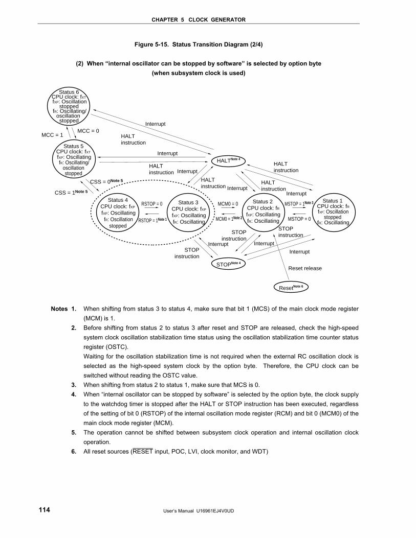
CHAPTER 5 CLOCK GENERATOR
User’s Manual U16961EJ4V0UD 114
Figure 5-15. Status Transition Diagram (2/4)
(2) When “internal oscillator can be stopped by software” is selected by option byte (when subsystem clock is used)
HALTNote 4Interrupt
Interrupt
Interrupt
Interrupt Interrupt
Interrupt
Interrupt
HALTinstruction
HALTinstruction
STOPinstruction
STOPinstruction
STOPinstruction
RSTOP = 0
RSTOP = 1Note 1
MCC = 0
CSS = 0Note 5
MCC = 1
CSS = 1Note 5
MCM0 = 0
MCM0 = 1Note 2
MSTOP = 1Note 3
MSTOP = 0
HALTinstruction
HALTinstruction
STOPNote 4
ResetNote 6
Status 4CPU clock: fXP fXP: OscillatingfR: Oscillation
stopped
Status 3CPU clock: fXP
fXP: OscillatingfR: Oscillating
Status 1CPU clock: fRfXP: Oscillation
stoppedfR: Oscillating
Status 2CPU clock: fRfXP: OscillatingfR: Oscillating
Reset release
Interrupt
HALTinstruction
Status 6CPU clock: fXT fXP: Oscillation
stoppedfR: Oscillating/
oscillation stopped
Status 5CPU clock: fXT fXP: OscillatingfR: Oscillating/
oscillationstopped
Notes 1. When shifting from status 3 to status 4, make sure that bit 1 (MCS) of the main clock mode register (MCM) is 1.
2. Before shifting from status 2 to status 3 after reset and STOP are released, check the high-speed system clock oscillation stabilization time status using the oscillation stabilization time counter status register (OSTC).
Waiting for the oscillation stabilization time is not required when the external RC oscillation clock is selected as the high-speed system clock by the option byte. Therefore, the CPU clock can be switched without reading the OSTC value.
3. When shifting from status 2 to status 1, make sure that MCS is 0. 4. When “internal oscillator can be stopped by software” is selected by the option byte, the clock supply
to the watchdog timer is stopped after the HALT or STOP instruction has been executed, regardless of the setting of bit 0 (RSTOP) of the internal oscillation mode register (RCM) and bit 0 (MCM0) of the main clock mode register (MCM).
5. The operation cannot be shifted between subsystem clock operation and internal oscillation clock operation.
6. All reset sources (RESET input, POC, LVI, clock monitor, and WDT)
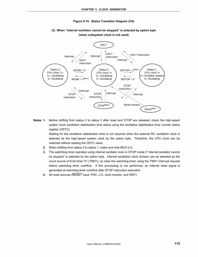
CHAPTER 5 CLOCK GENERATOR
User’s Manual U16961EJ4V0UD 115
Figure 5-15. Status Transition Diagram (3/4)
(3) When “internal oscillator cannot be stopped” is selected by option byte (when subsystem clock is not used)
Status 3CPU clock: fXP fXP: OscillatingfR: Oscillating
HALT
Interrupt Interrupt
InterruptSTOP
instruction
MCM0 = 0
MCM0 = 1Note 1
HALT instruction
HALT instruction
STOPNote 3
ResetNote 4
Status 2CPU clock: fRfXP: OscillatingfR: Oscillating
Status 1CPU clock: fR
fXP: Oscillation stoppedfR: Oscillating
InterruptSTOPinstruction
Interrupt
Interrupt
STOPinstruction
MSTOP = 1Note 2
MSTOP = 0
HALT instruction
Reset release
Notes 1. Before shifting from status 2 to status 3 after reset and STOP are released, check the high-speed system clock oscillation stabilization time status using the oscillation stabilization time counter status register (OSTC).
Waiting for the oscillation stabilization time is not required when the external RC oscillation clock is selected as the high-speed system clock by the option byte. Therefore, the CPU clock can be switched without reading the OSTC value.
2. When shifting from status 2 to status 1, make sure that MCS is 0. 3. The watchdog timer operates using internal oscillator even in STOP mode if “internal oscillator cannot
be stopped” is selected by the option byte. Internal oscillation clock division can be selected as the count source of 8-bit timer H1 (TMH1), so clear the watchdog timer using the TMH1 interrupt request before watchdog timer overflow. If this processing is not performed, an internal reset signal is generated at watchdog timer overflow after STOP instruction execution.
4. All reset sources (RESET input, POC, LVI, clock monitor, and WDT)
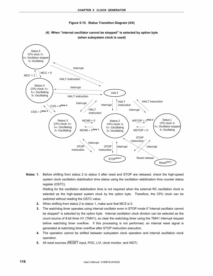
CHAPTER 5 CLOCK GENERATOR
User’s Manual U16961EJ4V0UD 116
Figure 5-15. Status Transition Diagram (4/4)
(4) When “internal oscillator cannot be stopped” is selected by option byte (when subsystem clock is used)
HALT
InterruptInterrupt
InterruptSTOP
instruction
MCM0 = 0
MCM0 = 1Note 1
HALTinstruction
HALT instruction
STOPNote 3
ResetNote 5
InterruptSTOPinstruction
Interrupt
Interrupt
STOPinstruction
MSTOP = 1Note 2
MSTOP = 0
HALT instruction
Reset release
MCC = 0
CSS = 0Note 4
MCC = 1
CSS = 1Note 4
Interrupt
Interrupt
HALT instruction
HALT instruction
Status 3CPU clock: fXP fXP: OscillatingfR: Oscillating
Status 2CPU clock: fRfXP: OscillatingfR: Oscillating
Status 1CPU clock: fR
fXP: Oscillation stoppedfR: Oscillating
Status 5CPU clock: fXT
fXP: Oscillation stoppedfR: Oscillating
Status 4CPU clock: fXT fXP: OscillatingfR: Oscillating
Notes 1. Before shifting from status 2 to status 3 after reset and STOP are released, check the high-speed system clock oscillation stabilization time status using the oscillation stabilization time counter status register (OSTC).
Waiting for the oscillation stabilization time is not required when the external RC oscillation clock is selected as the high-speed system clock by the option byte. Therefore, the CPU clock can be switched without reading the OSTC value.
2. When shifting from status 2 to status 1, make sure that MCS is 0. 3. The watchdog timer operates using internal oscillator even in STOP mode if “internal oscillator cannot
be stopped” is selected by the option byte. Internal oscillation clock division can be selected as the count source of 8-bit timer H1 (TMH1), so clear the watchdog timer using the TMH1 interrupt request before watchdog timer overflow. If this processing is not performed, an internal reset signal is generated at watchdog timer overflow after STOP instruction execution.
4. The operation cannot be shifted between subsystem clock operation and internal oscillation clock operation.
5. All reset sources (RESET input, POC, LVI, clock monitor, and WDT)
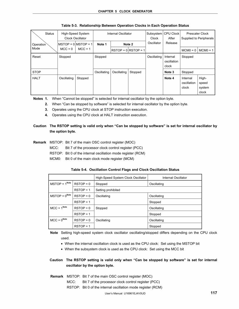
CHAPTER 5 CLOCK GENERATOR
User’s Manual U16961EJ4V0UD 117
Table 5-3. Relationship Between Operation Clocks in Each Operation Status
High-Speed System Clock Oscillator
Internal Oscillator
Note 2
Prescaler Clock Supplied to Peripherals
Status
Operation Mode
MSTOP = 0 MCC = 0
MSTOP = 1 MCC = 1
Note 1
RSTOP = 0 RSTOP = 1
Subsystem Clock
Oscillator
CPU Clock After
Release
MCM0 = 0 MCM0 = 1
Reset Stopped Internal oscillation clock
Stopped
STOP
Stopped
Note 3 Stopped
HALT Oscillating Stopped
Oscillating Oscillating Stopped
Oscillating
Note 4 Internal oscillation clock
High-speed system clock
Notes 1. When “Cannot be stopped” is selected for internal oscillator by the option byte. 2. When “Can be stopped by software” is selected for internal oscillator by the option byte. 3. Operates using the CPU clock at STOP instruction execution. 4. Operates using the CPU clock at HALT instruction execution. Caution The RSTOP setting is valid only when “Can be stopped by software” is set for internal oscillator by
the option byte. Remark MSTOP: Bit 7 of the main OSC control register (MOC) MCC: Bit 7 of the processor clock control register (PCC) RSTOP: Bit 0 of the internal oscillation mode register (RCM) MCM0: Bit 0 of the main clock mode register (MCM)
Table 5-4. Oscillation Control Flags and Clock Oscillation Status
High-Speed System Clock Oscillator Internal Oscillator
RSTOP = 0 Stopped Oscillating MSTOP = 1Note
RSTOP = 1 Setting prohibited
RSTOP = 0 Oscillating MSTOP = 0Note
RSTOP = 1
Oscillating
Stopped
RSTOP = 0 Oscillating MCC = 1Note
RSTOP = 1
Stopped
Stopped
RSTOP = 0 Oscillating MCC = 0Note
RSTOP = 1
Oscillating
Stopped
Note Setting high-speed system clock oscillator oscillating/stopped differs depending on the CPU clock used.
• When the internal oscillation clock is used as the CPU clock: Set using the MSTOP bit • When the subsystem clock is used as the CPU clock: Set using the MCC bit Caution The RSTOP setting is valid only when “Can be stopped by software” is set for internal
oscillator by the option byte.
Remark MSTOP: Bit 7 of the main OSC control register (MOC) MCC: Bit 7 of the processor clock control register (PCC) RSTOP: Bit 0 of the internal oscillation mode register (RCM)
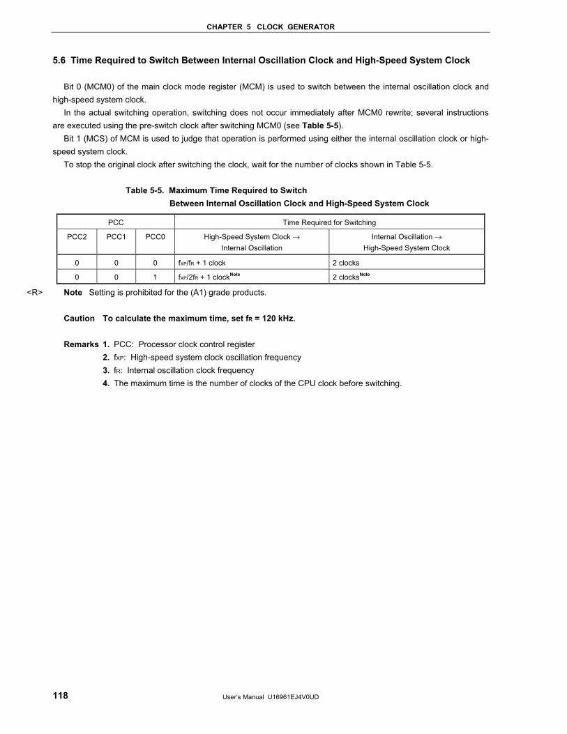
CHAPTER 5 CLOCK GENERATOR
User’s Manual U16961EJ4V0UD 118
5.6 Time Required to Switch Between Internal Oscillation Clock and High-Speed System Clock
Bit 0 (MCM0) of the main clock mode register (MCM) is used to switch between the internal oscillation clock and high-speed system clock.
In the actual switching operation, switching does not occur immediately after MCM0 rewrite; several instructions are executed using the pre-switch clock after switching MCM0 (see Table 5-5).
Bit 1 (MCS) of MCM is used to judge that operation is performed using either the internal oscillation clock or high-speed system clock.
To stop the original clock after switching the clock, wait for the number of clocks shown in Table 5-5.
Table 5-5. Maximum Time Required to Switch Between Internal Oscillation Clock and High-Speed System Clock
PCC Time Required for Switching
PCC2 PCC1 PCC0 High-Speed System Clock → Internal Oscillation
Internal Oscillation → High-Speed System Clock
0 0 0 fXP/fR + 1 clock 2 clocks
0 0 1 fXP/2fR + 1 clockNote 2 clocksNote
Note Setting is prohibited for the (A1) grade products.
Caution To calculate the maximum time, set fR = 120 kHz.
Remarks 1. PCC: Processor clock control register 2. fXP: High-speed system clock oscillation frequency 3. fR: Internal oscillation clock frequency 4. The maximum time is the number of clocks of the CPU clock before switching.
<R>
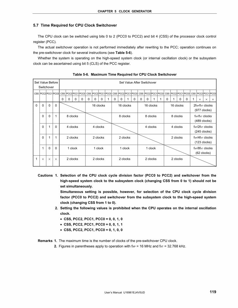
CHAPTER 5 CLOCK GENERATOR
User’s Manual U16961EJ4V0UD 119
5.7 Time Required for CPU Clock Switchover
The CPU clock can be switched using bits 0 to 2 (PCC0 to PCC2) and bit 4 (CSS) of the processor clock control register (PCC).
The actual switchover operation is not performed immediately after rewriting to the PCC; operation continues on the pre-switchover clock for several instructions (see Table 5-6).
Whether the system is operating on the high-speed system clock (or internal oscillation clock) or the subsystem clock can be ascertained using bit 5 (CLS) of the PCC register.
Table 5-6. Maximum Time Required for CPU Clock Switchover
Set Value Before Switchover
Set Value After Switchover
CSS PCC2 PCC1 PCC0 CSS PCC2 PCC1 PCC0 CSS PCC2 PCC1 PCC0 CSS PCC2 PCC1 PCC0 CSS PCC2 PCC1 PCC0 CSS PCC2 PCC1 PCC0CSS PCC2 PCC1 PCC0
0 0 0 0 0 0 0 1 0 0 1 0 0 0 1 1 0 1 0 0 1 × × ×
0 0 0 16 clocks 16 clocks 16 clocks 16 clocks 2fXP/fXT clocks (977 clocks)
0 0 1 8 clocks 8 clocks 8 clocks 8 clocks fXP/fXT clocks (489 clocks)
0 1 0 4 clocks 4 clocks 4 clocks 4 clocks fXP/2fXT clocks (245 clocks)
0 1 1 2 clocks 2 clocks 2 clocks 2 clocks fXP/4fXT clocks (123 clocks)
0
1 0 0 1 clock 1 clock 1 clock 1 clock fXP/8fXT clocks (62 clocks)
1 × × × 2 clocks 2 clocks 2 clocks 2 clocks 2 clocks
Cautions 1. Selection of the CPU clock cycle division factor (PCC0 to PCC2) and switchover from the
high-speed system clock to the subsystem clock (changing CSS from 0 to 1) should not be set simultaneously.
Simultaneous setting is possible, however, for selection of the CPU clock cycle division factor (PCC0 to PCC2) and switchover from the subsystem clock to the high-speed system clock (changing CSS from 1 to 0).
2. Setting the following values is prohibited when the CPU operates on the internal oscillation clock.
• CSS, PCC2, PCC1, PCC0 = 0, 0, 1, 0 • CSS, PCC2, PCC1, PCC0 = 0, 0, 1, 1 • CSS, PCC2, PCC1, PCC0 = 0, 1, 0, 0
Remarks 1. The maximum time is the number of clocks of the pre-switchover CPU clock. 2. Figures in parentheses apply to operation with fXP = 16 MHz and fXT = 32.768 kHz.
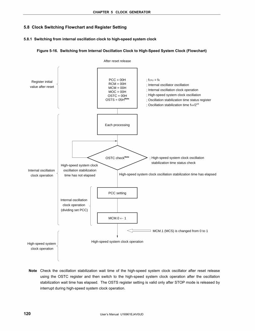
CHAPTER 5 CLOCK GENERATOR
User’s Manual U16961EJ4V0UD 120
5.8 Clock Switching Flowchart and Register Setting 5.8.1 Switching from internal oscillation clock to high-speed system clock
Figure 5-16. Switching from Internal Oscillation Clock to High-Speed System Clock (Flowchart)
; fCPU = fR
; Internal oscillator oscillation
; Internal oscillation clock operation
; High-speed system clock oscillation
; Oscillation stabilization time status register
; Oscillation stabilization time fXP/216
MCM.1 (MCS) is changed from 0 to 1
; High-speed system clock oscillation
stabilization time status check
High-speed system clock oscillation stabilization time has elapsed
High-speed system clock
oscillation stabilization
time has not elapsed
PCC = 00HRCM = 00HMCM = 00HMOC = 00HOSTC = 00H
OSTS = 05HNote
OSTC checkNote
Each processing
After reset release
PCC setting
MCM.0 ← 1
High-speed system clock operation
Internal oscillation
clock operation
(dividing set PCC)
Register initial
value after reset
Internal oscillation
clock operation
High-speed system
clock operation
Note Check the oscillation stabilization wait time of the high-speed system clock oscillator after reset release using the OSTC register and then switch to the high-speed system clock operation after the oscillation stabilization wait time has elapsed. The OSTS register setting is valid only after STOP mode is released by interrupt during high-speed system clock operation.
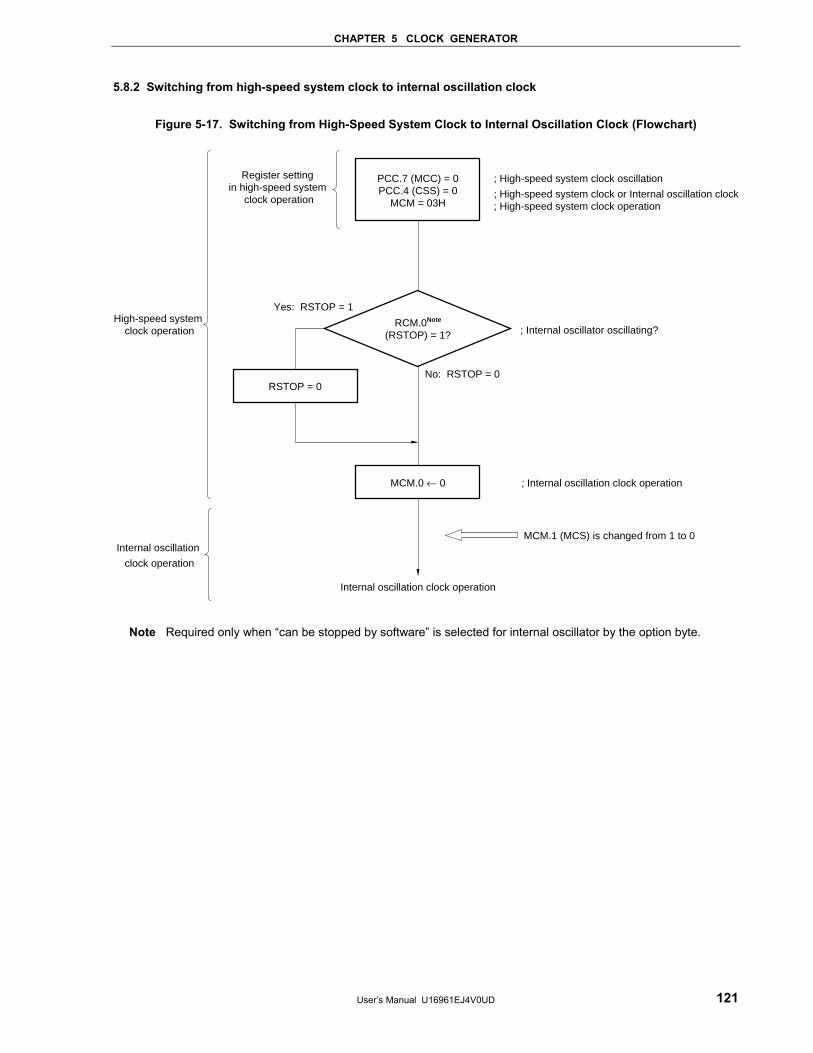
CHAPTER 5 CLOCK GENERATOR
User’s Manual U16961EJ4V0UD 121
5.8.2 Switching from high-speed system clock to internal oscillation clock
Figure 5-17. Switching from High-Speed System Clock to Internal Oscillation Clock (Flowchart)
MCM.1 (MCS) is changed from 1 to 0
; Internal oscillation clock operation
; Internal oscillator oscillating?
Internal oscillation clock operation
; High-speed system clock oscillation
; High-speed system clock or Internal oscillation clock; High-speed system clock operation
No: RSTOP = 0
Yes: RSTOP = 1
PCC.7 (MCC) = 0PCC.4 (CSS) = 0
MCM = 03H
RCM.0Note
(RSTOP) = 1?
RSTOP = 0
MCM.0 ← 0
Register setting in high-speed system
clock operation
High-speed system clock operation
Internal oscillation
clock operation
Note Required only when “can be stopped by software” is selected for internal oscillator by the option byte.
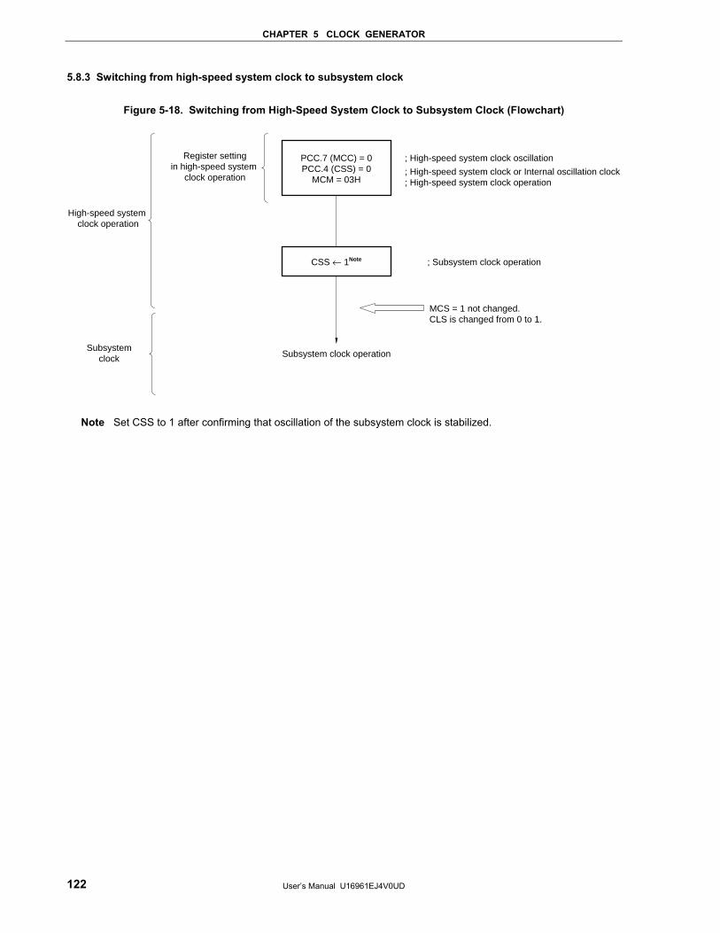
CHAPTER 5 CLOCK GENERATOR
User’s Manual U16961EJ4V0UD 122
5.8.3 Switching from high-speed system clock to subsystem clock
Figure 5-18. Switching from High-Speed System Clock to Subsystem Clock (Flowchart)
MCS = 1 not changed.CLS is changed from 0 to 1.
; Subsystem clock operation
Subsystem clock operation
; High-speed system clock oscillation
; High-speed system clock or Internal oscillation clock; High-speed system clock operation
PCC.7 (MCC) = 0PCC.4 (CSS) = 0
MCM = 03H
CSS ← 1Note
Register settingin high-speed system
clock operation
High-speed system clock operation
Subsystemclock
Note Set CSS to 1 after confirming that oscillation of the subsystem clock is stabilized.
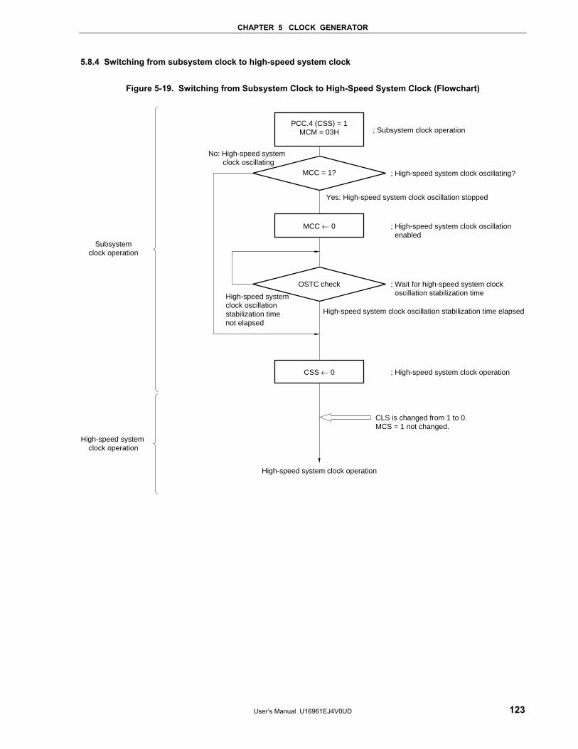
CHAPTER 5 CLOCK GENERATOR
User’s Manual U16961EJ4V0UD 123
5.8.4 Switching from subsystem clock to high-speed system clock
Figure 5-19. Switching from Subsystem Clock to High-Speed System Clock (Flowchart)
; Subsystem clock operation
; High-speed system clock oscillating?
; High-speed system clock oscillation enabled
; Wait for high-speed system clock oscillation stabilization time
; High-speed system clock operation
CLS is changed from 1 to 0.MCS = 1 not changed.
High-speed system clock oscillation stabilization time elapsed
High-speed system clock oscillation stabilization time not elapsed
Yes: High-speed system clock oscillation stopped
No: High-speed system clock oscillating
MCC ← 0
PCC.4 (CSS) = 1MCM = 03H
MCC = 1?
OSTC check
CSS ← 0
High-speed system clock operation
Subsystemclock operation
High-speed system clock operation
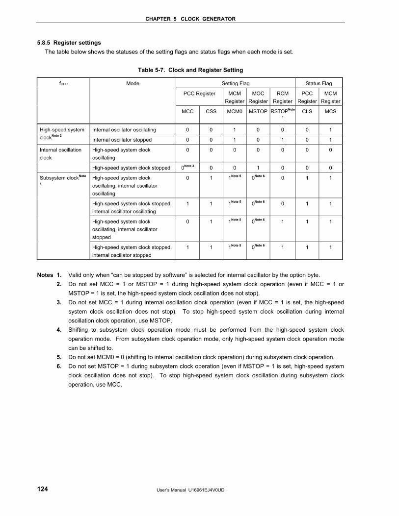
CHAPTER 5 CLOCK GENERATOR
User’s Manual U16961EJ4V0UD 124
5.8.5 Register settings The table below shows the statuses of the setting flags and status flags when each mode is set.
Table 5-7. Clock and Register Setting
Setting Flag Status Flag
PCC Register MCM Register
MOC Register
RCM Register
PCC Register
MCM Register
fCPU Mode
MCC CSS MCM0 MSTOP RSTOPNote
1 CLS MCS
Internal oscillator oscillating 0 0 1 0 0 0 1 High-speed system clockNote 2 Internal oscillator stopped 0 0 1 0 1 0 1
High-speed system clock oscillating
0 0 0 0 0 0 0 Internal oscillation clock
High-speed system clock stopped 0Note 3 0 0 1 0 0 0
High-speed system clock oscillating, internal oscillator oscillating
0 1 1Note 5 0Note 6 0 1 1
High-speed system clock stopped, internal oscillator oscillating
1 1 1Note 5 0Note 6 0 1 1
High-speed system clock oscillating, internal oscillator stopped
0 1 1Note 5 0Note 6 1 1 1
Subsystem clockNote
4
High-speed system clock stopped, internal oscillator stopped
1 1 1Note 5 0Note 6 1 1 1
Notes 1. Valid only when “can be stopped by software” is selected for internal oscillator by the option byte. 2. Do not set MCC = 1 or MSTOP = 1 during high-speed system clock operation (even if MCC = 1 or
MSTOP = 1 is set, the high-speed system clock oscillation does not stop). 3. Do not set MCC = 1 during internal oscillation clock operation (even if MCC = 1 is set, the high-speed
system clock oscillation does not stop). To stop high-speed system clock oscillation during internal oscillation clock operation, use MSTOP.
4. Shifting to subsystem clock operation mode must be performed from the high-speed system clock operation mode. From subsystem clock operation mode, only high-speed system clock operation mode can be shifted to.
5. Do not set MCM0 = 0 (shifting to internal oscillation clock operation) during subsystem clock operation. 6. Do not set MSTOP = 1 during subsystem clock operation (even if MSTOP = 1 is set, high-speed system
clock oscillation does not stop). To stop high-speed system clock oscillation during subsystem clock operation, use MCC.
User’s Manual U16961EJ4V0UD 125
CHAPTER 6 16-BIT TIMER/EVENT COUNTER 00
6.1 Functions of 16-Bit Timer/Event Counter 00
16-bit timer/event counter 00 has the following functions.
• Interval timer
• PPG output
• Pulse width measurement
• External event counter
• Square-wave output
• One-shot pulse output
(1) Interval timer
16-bit timer/event counter 00 generates an interrupt request at the preset time interval.
(2) PPG output
16-bit timer/event counter 00 can output a rectangular wave whose frequency and output pulse width can be set
freely.
(3) Pulse width measurement
16-bit timer/event counter 00 can measure the pulse width of an externally input signal.
(4) External event counter
16-bit timer/event counter 00 can measure the number of pulses of an externally input signal.
(5) Square-wave output
16-bit timer/event counter 00 can output a square wave with any selected frequency.
(6) One-shot pulse output
16-bit timer/event counter 00 can output a one-shot pulse whose output pulse width can be set freely.
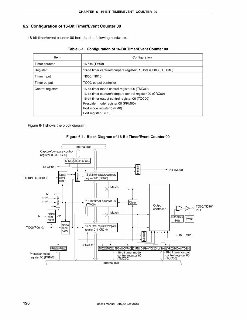
CHAPTER 6 16-BIT TIMER/EVENT COUNTER 00
User’s Manual U16961EJ4V0UD 126
6.2 Configuration of 16-Bit Timer/Event Counter 00
16-bit timer/event counter 00 includes the following hardware.
Table 6-1. Configuration of 16-Bit Timer/Event Counter 00
Item Configuration
Timer counter 16 bits (TM00)
Register 16-bit timer capture/compare register: 16 bits (CR000, CR010)
Timer input TI000, TI010
Timer output TO00, output controller
Control registers 16-bit timer mode control register 00 (TMC00)
16-bit timer capture/compare control register 00 (CRC00)
16-bit timer output control register 00 (TOC00)
Prescaler mode register 00 (PRM00)
Port mode register 0 (PM0)
Port register 0 (P0)
Figure 6-1 shows the block diagram.
Figure 6-1. Block Diagram of 16-Bit Timer/Event Counter 00
Internal bus
Capture/compare controlregister 00 (CRC00)
TI010/TO00/P01
fXfX/22
fX/28
fX
TI000/P00
Prescaler moderegister 00 (PRM00)
2
PRM001 PRM000CRC002
16-bit timer capture/compareregister 010 (CR010)
Match
Match
16-bit timer counter 00(TM00)
Clear
Noiseelimi-nator
CRC002 CRC001 CRC000
INTTM000
TO00/TI010/P01
INTTM010
16-bit timer output control register 00 (TOC00)
16-bit timer modecontrol register 00(TMC00)
Internal bus
TMC003 TMC002 TMC001 OVF00 TOC004 LVS00 LVR00 TOC001 TOE00
Sel
ecto
r
16-bit timer capture/compareregister 000 (CR000)
Sel
ecto
r
Sel
ecto
r
Sel
ecto
r
Noiseelimi-nator
Noiseelimi-nator
Outputcontroller
OSPE00OSPT00
Output latch(P01)
PM01
To CR010
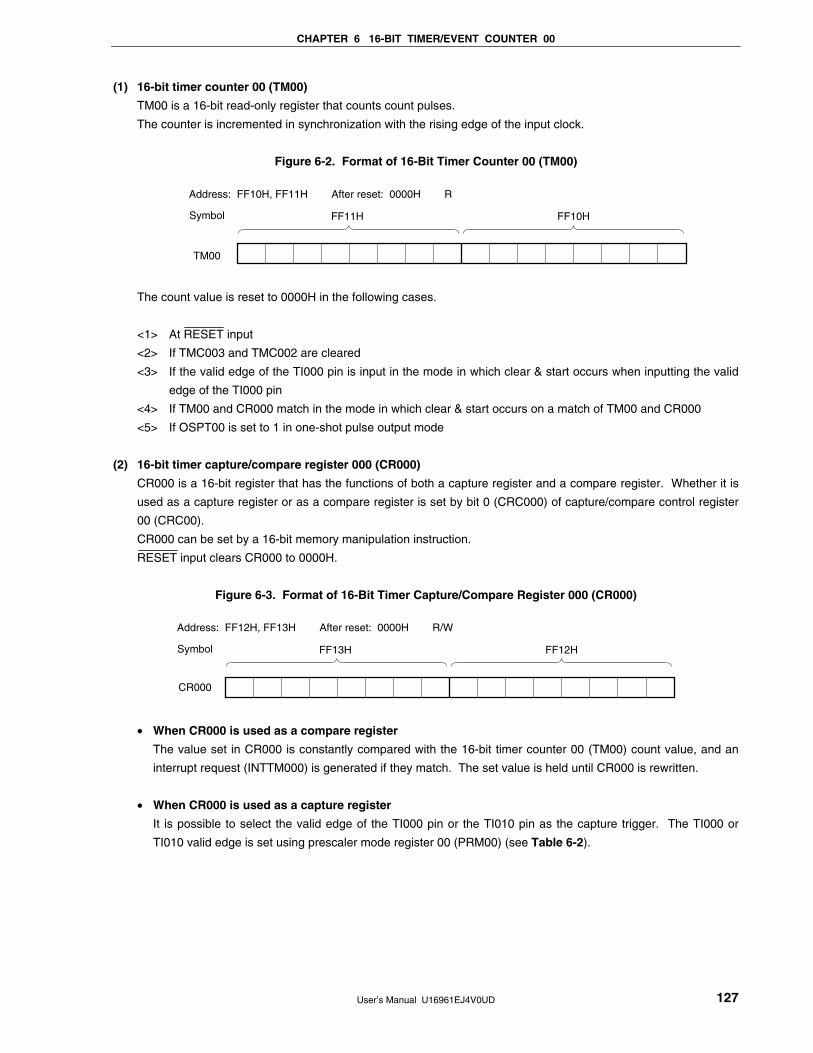
CHAPTER 6 16-BIT TIMER/EVENT COUNTER 00
User’s Manual U16961EJ4V0UD 127
(1) 16-bit timer counter 00 (TM00)
TM00 is a 16-bit read-only register that counts count pulses.
The counter is incremented in synchronization with the rising edge of the input clock.
Figure 6-2. Format of 16-Bit Timer Counter 00 (TM00)
TM00
Symbol FF11H FF10H
Address: FF10H, FF11H After reset: 0000H R
The count value is reset to 0000H in the following cases.
<1> At RESET input
<2> If TMC003 and TMC002 are cleared
<3> If the valid edge of the TI000 pin is input in the mode in which clear & start occurs when inputting the valid
edge of the TI000 pin
<4> If TM00 and CR000 match in the mode in which clear & start occurs on a match of TM00 and CR000
<5> If OSPT00 is set to 1 in one-shot pulse output mode
(2) 16-bit timer capture/compare register 000 (CR000)
CR000 is a 16-bit register that has the functions of both a capture register and a compare register. Whether it is
used as a capture register or as a compare register is set by bit 0 (CRC000) of capture/compare control register
00 (CRC00).
CR000 can be set by a 16-bit memory manipulation instruction.
RESET input clears CR000 to 0000H.
Figure 6-3. Format of 16-Bit Timer Capture/Compare Register 000 (CR000)
CR000
Symbol FF13H FF12H
Address: FF12H, FF13H After reset: 0000H R/W
• When CR000 is used as a compare register
The value set in CR000 is constantly compared with the 16-bit timer counter 00 (TM00) count value, and an
interrupt request (INTTM000) is generated if they match. The set value is held until CR000 is rewritten.
• When CR000 is used as a capture register
It is possible to select the valid edge of the TI000 pin or the TI010 pin as the capture trigger. The TI000 or
TI010 valid edge is set using prescaler mode register 00 (PRM00) (see Table 6-2).
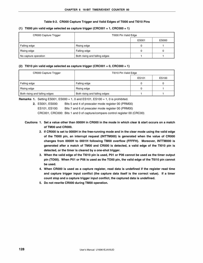
CHAPTER 6 16-BIT TIMER/EVENT COUNTER 00
User’s Manual U16961EJ4V0UD 128
Table 6-2. CR000 Capture Trigger and Valid Edges of TI000 and TI010 Pins
(1) TI000 pin valid edge selected as capture trigger (CRC001 = 1, CRC000 = 1)
TI000 Pin Valid Edge CR000 Capture Trigger
ES001 ES000
Falling edge Rising edge 0 1
Rising edge Falling edge 0 0
No capture operation Both rising and falling edges 1 1
(2) TI010 pin valid edge selected as capture trigger (CRC001 = 0, CRC000 = 1)
TI010 Pin Valid Edge CR000 Capture Trigger
ES101 ES100
Falling edge Falling edge 0 0
Rising edge Rising edge 0 1
Both rising and falling edges Both rising and falling edges 1 1
Remarks 1. Setting ES001, ES000 = 1, 0 and ES101, ES100 = 1, 0 is prohibited.
2. ES001, ES000: Bits 5 and 4 of prescaler mode register 00 (PRM00)
ES101, ES100: Bits 7 and 6 of prescaler mode register 00 (PRM00)
CRC001, CRC000: Bits 1 and 0 of capture/compare control register 00 (CRC00)
Cautions 1. Set a value other than 0000H in CR000 in the mode in which clear & start occurs on a match
of TM00 and CR000.
2. If CR000 is set to 0000H in the free-running mode and in the clear mode using the valid edge
of the TI000 pin, an interrupt request (INTTM000) is generated when the value of CR000
changes from 0000H to 0001H following TM00 overflow (FFFFH). Moreover, INTTM000 is
generated after a match of TM00 and CR000 is detected, a valid edge of the TI010 pin is
detected, or the timer is cleared by a one-shot trigger.
3. When the valid edge of the TI010 pin is used, P01 or P06 cannot be used as the timer output
pin (TO00). When P01 or P06 is used as the TO00 pin, the valid edge of the TI010 pin cannot
be used.
4. When CR000 is used as a capture register, read data is undefined if the register read time
and capture trigger input conflict (the capture data itself is the correct value). If a timer
count stop and a capture trigger input conflict, the captured data is undefined.
5. Do not rewrite CR000 during TM00 operation.
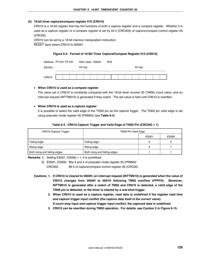
CHAPTER 6 16-BIT TIMER/EVENT COUNTER 00
User’s Manual U16961EJ4V0UD 129
(3) 16-bit timer capture/compare register 010 (CR010)
CR010 is a 16-bit register that has the functions of both a capture register and a compare register. Whether it is
used as a capture register or a compare register is set by bit 2 (CRC002) of capture/compare control register 00
(CRC00).
CR010 can be set by a 16-bit memory manipulation instruction.
RESET input clears CR010 to 0000H.
Figure 6-4. Format of 16-Bit Timer Capture/Compare Register 010 (CR010)
CR010
Symbol FF15H FF14H
Address: FF14H, FF15H After reset: 0000H R/W
• When CR010 is used as a compare register
The value set in CR010 is constantly compared with the 16-bit timer counter 00 (TM00) count value, and an
interrupt request (INTTM010) is generated if they match. The set value is held until CR010 is rewritten.
• When CR010 is used as a capture register
It is possible to select the valid edge of the TI000 pin as the capture trigger. The TI000 pin valid edge is set
using prescaler mode register 00 (PRM00) (see Table 6-3).
Table 6-3. CR010 Capture Trigger and Valid Edge of TI000 Pin (CRC002 = 1)
TI000 Pin Valid Edge CR010 Capture Trigger
ES001 ES000
Falling edge Falling edge 0 0
Rising edge Rising edge 0 1
Both rising and falling edges Both rising and falling edges 1 1
Remarks 1. Setting ES001, ES000 = 1, 0 is prohibited.
2. ES001, ES000: Bits 5 and 4 of prescaler mode register 00 (PRM00)
CRC002: Bit 2 of capture/compare control register 00 (CRC00)
Cautions 1. If CR010 is cleared to 0000H, an interrupt request (INTTM010) is generated when the value of
CR010 changes from 0000H to 0001H following TM00 overflow (FFFFH). Moreover,
INTTM010 is generated after a match of TM00 and CR010 is detected, a valid edge of the
TI000 pin is detected, or the timer is cleared by a one-shot trigger.
2. When CR010 is used as a capture register, read data is undefined if the register read time
and capture trigger input conflict (the capture data itself is the correct value).
If count stop input and capture trigger input conflict, the captured data is undefined.
3. CR010 can be rewritten during TM00 operation. For details, see Caution 2 in Figure 6-15.
CHAPTER 6 16-BIT TIMER/EVENT COUNTER 00
User’s Manual U16961EJ4V0UD 130
6.3 Registers Controlling 16-Bit Timer/Event Counter 00
The following six registers are used to control 16-bit timer/event counter 00.
• 16-bit timer mode control register 00 (TMC00)
• Capture/compare control register 00 (CRC00)
• 16-bit timer output control register 00 (TOC00)
• Prescaler mode register 00 (PRM00)
• Port mode register 0 (PM0)
• Port register 0 (P0)
(1) 16-bit timer mode control register 00 (TMC00)
This register sets the 16-bit timer operating mode, the 16-bit timer counter 00 (TM00) clear mode, and output
timing, and detects an overflow.
TMC00 can be set by a 1-bit or 8-bit memory manipulation instruction.
RESET input clears TMC00 to 00H.
Caution 16-bit timer counter 00 (TM00) starts operation at the moment TMC002 and TMC003 are set to
values other than 0, 0 (operation stop mode), respectively. Set TMC002 and TMC003 to 0, 0 to
stop the operation.
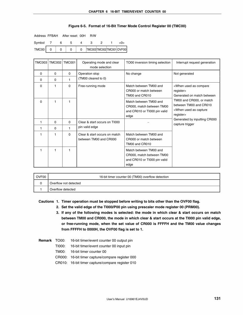
CHAPTER 6 16-BIT TIMER/EVENT COUNTER 00
User’s Manual U16961EJ4V0UD 131
Figure 6-5. Format of 16-Bit Timer Mode Control Register 00 (TMC00)
7
0
6
0
5
0
4
0
3
TMC003
2
TMC002
1
TMC001
<0>
OVF00
Symbol
TMC00
Address FFBAH After reset: 00H R/W
TMC003 TMC002 TMC001 Operating mode and clear
mode selection
TO00 inversion timing selection Interrupt request generation
0 0 0
0 0 1
Operation stop
(TM00 cleared to 0)
No change Not generated
0 1 0 Free-running mode Match between TM00 and
CR000 or match between
TM00 and CR010
0 1 1 Match between TM00 and
CR000, match between TM00
and CR010 or TI000 pin valid
edge
1 0 0
1 0 1
Clear & start occurs on TI000
pin valid edge
−
1 1 0 Clear & start occurs on match
between TM00 and CR000
Match between TM00 and
CR000 or match between
TM00 and CR010
1 1 1 Match between TM00 and
CR000, match between TM00
and CR010 or TI000 pin valid
edge
<When used as compare
register>
Generated on match between
TM00 and CR000, or match
between TM00 and CR010
<When used as capture
register>
Generated by inputting CR000
capture trigger
OVF00 16-bit timer counter 00 (TM00) overflow detection
0 Overflow not detected
1 Overflow detected
Cautions 1. Timer operation must be stopped before writing to bits other than the OVF00 flag.
2. Set the valid edge of the TI000/P00 pin using prescaler mode register 00 (PRM00).
3. If any of the following modes is selected: the mode in which clear & start occurs on match
between TM00 and CR000, the mode in which clear & start occurs at the TI000 pin valid edge,
or free-running mode, when the set value of CR000 is FFFFH and the TM00 value changes
from FFFFH to 0000H, the OVF00 flag is set to 1.
Remark TO00: 16-bit timer/event counter 00 output pin
TI000: 16-bit timer/event counter 00 input pin
TM00: 16-bit timer counter 00
CR000: 16-bit timer capture/compare register 000
CR010: 16-bit timer capture/compare register 010
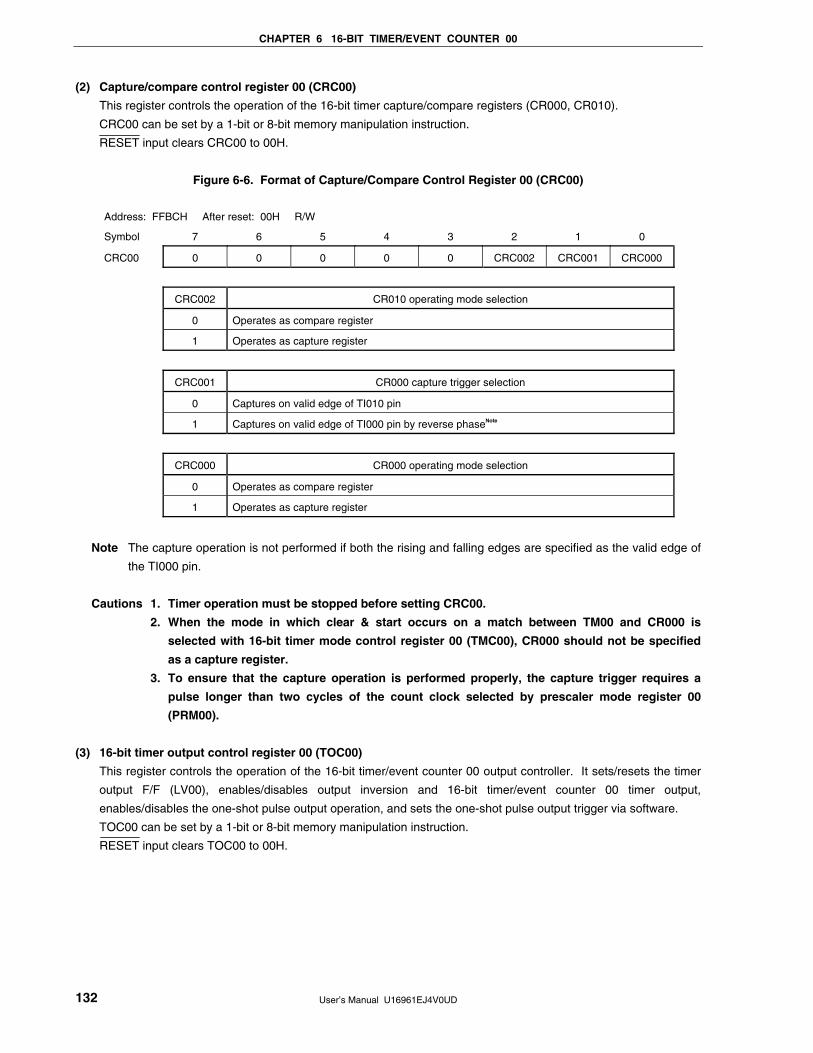
CHAPTER 6 16-BIT TIMER/EVENT COUNTER 00
User’s Manual U16961EJ4V0UD 132
(2) Capture/compare control register 00 (CRC00)
This register controls the operation of the 16-bit timer capture/compare registers (CR000, CR010).
CRC00 can be set by a 1-bit or 8-bit memory manipulation instruction.
RESET input clears CRC00 to 00H.
Figure 6-6. Format of Capture/Compare Control Register 00 (CRC00)
Address: FFBCH After reset: 00H R/W
Symbol 7 6 5 4 3 2 1 0
CRC00 0 0 0 0 0 CRC002 CRC001 CRC000
CRC002 CR010 operating mode selection
0 Operates as compare register
1 Operates as capture register
CRC001 CR000 capture trigger selection
0 Captures on valid edge of TI010 pin
1 Captures on valid edge of TI000 pin by reverse phaseNote
CRC000 CR000 operating mode selection
0 Operates as compare register
1 Operates as capture register
Note The capture operation is not performed if both the rising and falling edges are specified as the valid edge of
the TI000 pin.
Cautions 1. Timer operation must be stopped before setting CRC00.
2. When the mode in which clear & start occurs on a match between TM00 and CR000 is
selected with 16-bit timer mode control register 00 (TMC00), CR000 should not be specified
as a capture register.
3. To ensure that the capture operation is performed properly, the capture trigger requires a
pulse longer than two cycles of the count clock selected by prescaler mode register 00
(PRM00).
(3) 16-bit timer output control register 00 (TOC00)
This register controls the operation of the 16-bit timer/event counter 00 output controller. It sets/resets the timer
output F/F (LV00), enables/disables output inversion and 16-bit timer/event counter 00 timer output,
enables/disables the one-shot pulse output operation, and sets the one-shot pulse output trigger via software.
TOC00 can be set by a 1-bit or 8-bit memory manipulation instruction.
RESET input clears TOC00 to 00H.
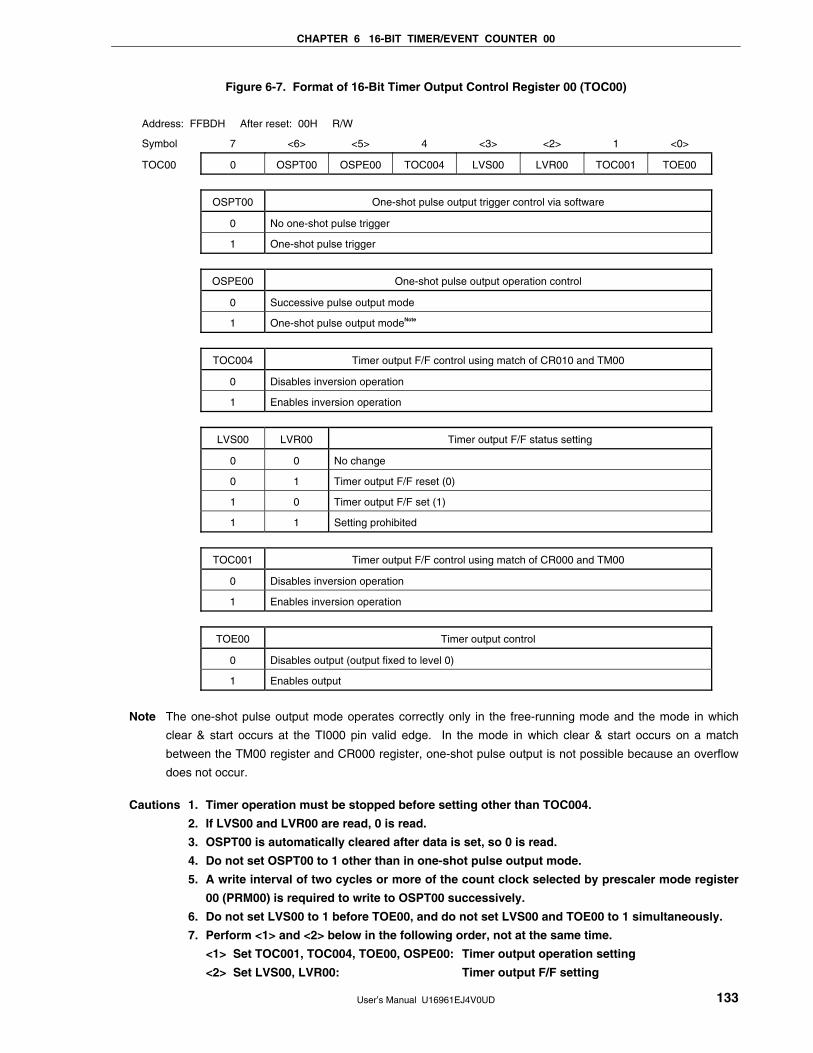
CHAPTER 6 16-BIT TIMER/EVENT COUNTER 00
User’s Manual U16961EJ4V0UD 133
Figure 6-7. Format of 16-Bit Timer Output Control Register 00 (TOC00)
Address: FFBDH After reset: 00H R/W
Symbol 7 <6> <5> 4 <3> <2> 1 <0>
TOC00 0 OSPT00 OSPE00 TOC004 LVS00 LVR00 TOC001 TOE00
OSPT00 One-shot pulse output trigger control via software
0 No one-shot pulse trigger
1 One-shot pulse trigger
OSPE00 One-shot pulse output operation control
0 Successive pulse output mode
1 One-shot pulse output modeNote
TOC004 Timer output F/F control using match of CR010 and TM00
0 Disables inversion operation
1 Enables inversion operation
LVS00 LVR00 Timer output F/F status setting
0 0 No change
0 1 Timer output F/F reset (0)
1 0 Timer output F/F set (1)
1 1 Setting prohibited
TOC001 Timer output F/F control using match of CR000 and TM00
0 Disables inversion operation
1 Enables inversion operation
TOE00 Timer output control
0 Disables output (output fixed to level 0)
1 Enables output
Note The one-shot pulse output mode operates correctly only in the free-running mode and the mode in which
clear & start occurs at the TI000 pin valid edge. In the mode in which clear & start occurs on a match
between the TM00 register and CR000 register, one-shot pulse output is not possible because an overflow
does not occur.
Cautions 1. Timer operation must be stopped before setting other than TOC004.
2. If LVS00 and LVR00 are read, 0 is read.
3. OSPT00 is automatically cleared after data is set, so 0 is read.
4. Do not set OSPT00 to 1 other than in one-shot pulse output mode.
5. A write interval of two cycles or more of the count clock selected by prescaler mode register
00 (PRM00) is required to write to OSPT00 successively.
6. Do not set LVS00 to 1 before TOE00, and do not set LVS00 and TOE00 to 1 simultaneously.
7. Perform <1> and <2> below in the following order, not at the same time.
<1> Set TOC001, TOC004, TOE00, OSPE00: Timer output operation setting
<2> Set LVS00, LVR00: Timer output F/F setting
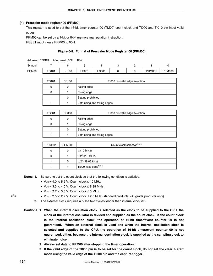
CHAPTER 6 16-BIT TIMER/EVENT COUNTER 00
User’s Manual U16961EJ4V0UD 134
(4) Prescaler mode register 00 (PRM00)
This register is used to set the 16-bit timer counter 00 (TM00) count clock and TI000 and TI010 pin input valid
edges.
PRM00 can be set by a 1-bit or 8-bit memory manipulation instruction.
RESET input clears PRM00 to 00H.
Figure 6-8. Format of Prescaler Mode Register 00 (PRM00)
Address: FFBBH After reset: 00H R/W
Symbol 7 6 5 4 3 2 1 0
PRM00 ES101 ES100 ES001 ES000 0 0 PRM001 PRM000
ES101 ES100 TI010 pin valid edge selection
0 0 Falling edge
0 1 Rising edge
1 0 Setting prohibited
1 1 Both rising and falling edges
ES001 ES000 TI000 pin valid edge selection
0 0 Falling edge
0 1 Rising edge
1 0 Setting prohibited
1 1 Both rising and falling edges
PRM001 PRM000 Count clock selectionNote 1
0 0 fX (10 MHz)
0 1 fX/22 (2.5 MHz)
1 0 fX/28 (39.06 kHz)
1 1 TI000 valid edgeNote 2
Notes 1. Be sure to set the count clock so that the following condition is satisfied.
• VDD = 4.0 to 5.5 V: Count clock ≤ 10 MHz
• VDD = 3.3 to 4.0 V: Count clock ≤ 8.38 MHz
• VDD = 2.7 to 3.3 V: Count clock ≤ 5 MHz
• VDD = 2.5 to 2.7 V: Count clock ≤ 2.5 MHz (standard products, (A) grade products only)
2. The external clock requires a pulse two cycles longer than internal clock (fX).
Cautions 1. When the internal oscillation clock is selected as the clock to be supplied to the CPU, the
clock of the internal oscillator is divided and supplied as the count clock. If the count clock
is the internal oscillation clock, the operation of 16-bit timer/event counter 00 is not
guaranteed. When an external clock is used and when the internal oscillation clock is
selected and supplied to the CPU, the operation of 16-bit timer/event counter 00 is not
guaranteed, either, because the internal oscillation clock is supplied as the sampling clock to
eliminate noise.
2. Always set data to PRM00 after stopping the timer operation.
3. If the valid edge of the TI000 pin is to be set for the count clock, do not set the clear & start
mode using the valid edge of the TI000 pin and the capture trigger.
<R>
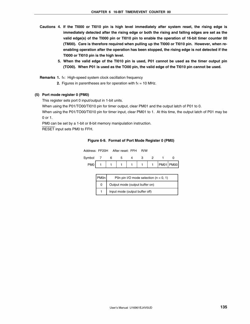
CHAPTER 6 16-BIT TIMER/EVENT COUNTER 00
User’s Manual U16961EJ4V0UD 135
Cautions 4. If the TI000 or TI010 pin is high level immediately after system reset, the rising edge is
immediately detected after the rising edge or both the rising and falling edges are set as the
valid edge(s) of the TI000 pin or TI010 pin to enable the operation of 16-bit timer counter 00
(TM00). Care is therefore required when pulling up the TI000 or TI010 pin. However, when re-
enabling operation after the operation has been stopped, the rising edge is not detected if the
TI000 or TI010 pin is the high level.
5. When the valid edge of the TI010 pin is used, P01 cannot be used as the timer output pin
(TO00). When P01 is used as the TO00 pin, the valid edge of the TI010 pin cannot be used.
Remarks 1. fX: High-speed system clock oscillation frequency
2. Figures in parentheses are for operation with fX = 10 MHz.
(5) Port mode register 0 (PM0)
This register sets port 0 input/output in 1-bit units.
When using the P01/TO00/TI010 pin for timer output, clear PM01 and the output latch of P01 to 0.
When using the P01/TO00/TI010 pin for timer input, clear PM01 to 1. At this time, the output latch of P01 may be
0 or 1.
PM0 can be set by a 1-bit or 8-bit memory manipulation instruction.
RESET input sets PM0 to FFH.
Figure 6-9. Format of Port Mode Register 0 (PM0)
7
1
6
1
5
1
4
1
3
1
2
1
1
PM01
0
PM00
Symbol
PM0
Address: FF20H After reset: FFH R/W
PM0n
0
1
P0n pin I/O mode selection (n = 0, 1)
Output mode (output buffer on)
Input mode (output buffer off)
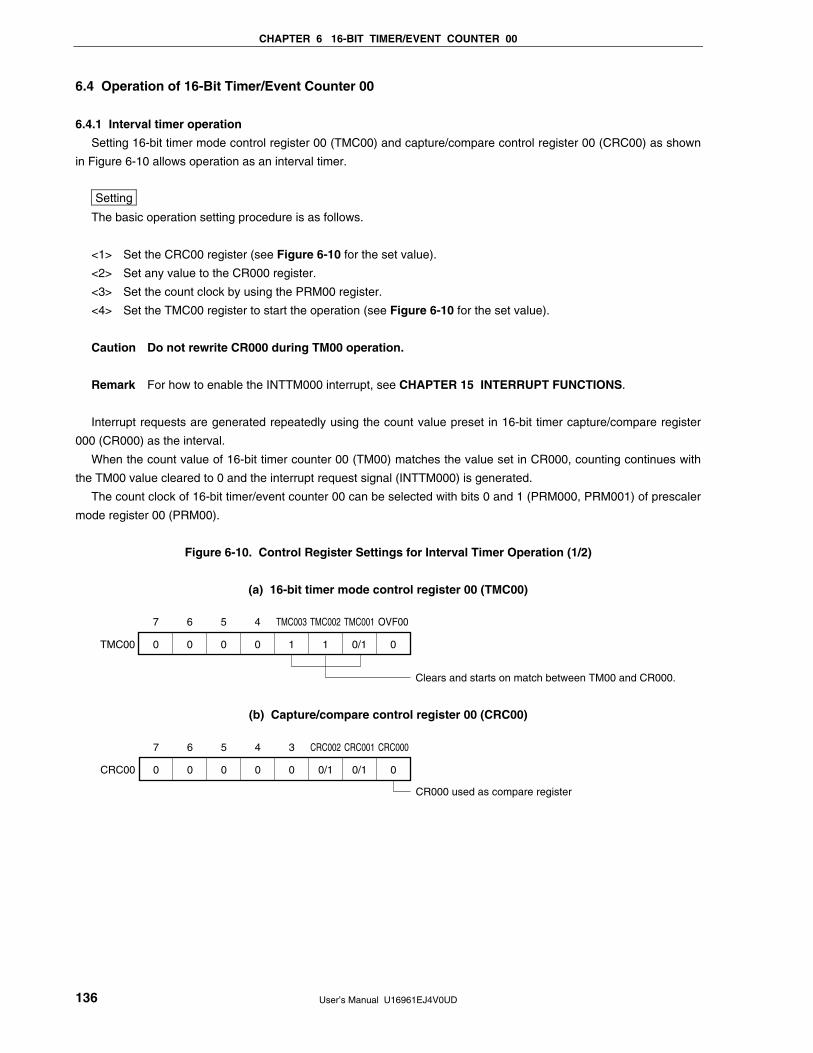
CHAPTER 6 16-BIT TIMER/EVENT COUNTER 00
User’s Manual U16961EJ4V0UD 136
6.4 Operation of 16-Bit Timer/Event Counter 00
6.4.1 Interval timer operation
Setting 16-bit timer mode control register 00 (TMC00) and capture/compare control register 00 (CRC00) as shown
in Figure 6-10 allows operation as an interval timer.
Setting
The basic operation setting procedure is as follows.
<1> Set the CRC00 register (see Figure 6-10 for the set value).
<2> Set any value to the CR000 register.
<3> Set the count clock by using the PRM00 register.
<4> Set the TMC00 register to start the operation (see Figure 6-10 for the set value).
Caution Do not rewrite CR000 during TM00 operation.
Remark For how to enable the INTTM000 interrupt, see CHAPTER 15 INTERRUPT FUNCTIONS.
Interrupt requests are generated repeatedly using the count value preset in 16-bit timer capture/compare register
000 (CR000) as the interval.
When the count value of 16-bit timer counter 00 (TM00) matches the value set in CR000, counting continues with
the TM00 value cleared to 0 and the interrupt request signal (INTTM000) is generated.
The count clock of 16-bit timer/event counter 00 can be selected with bits 0 and 1 (PRM000, PRM001) of prescaler
mode register 00 (PRM00).
Figure 6-10. Control Register Settings for Interval Timer Operation (1/2)
(a) 16-bit timer mode control register 00 (TMC00)
7
0
6
0
5
0
4
0
TMC003
1
TMC002
1
TMC001
0/1
OVF00
0TMC00
Clears and starts on match between TM00 and CR000.
(b) Capture/compare control register 00 (CRC00)
7
0
6
0
5
0
4
0
3
0
CRC002
0/1
CRC001
0/1
CRC000
0CRC00
CR000 used as compare register
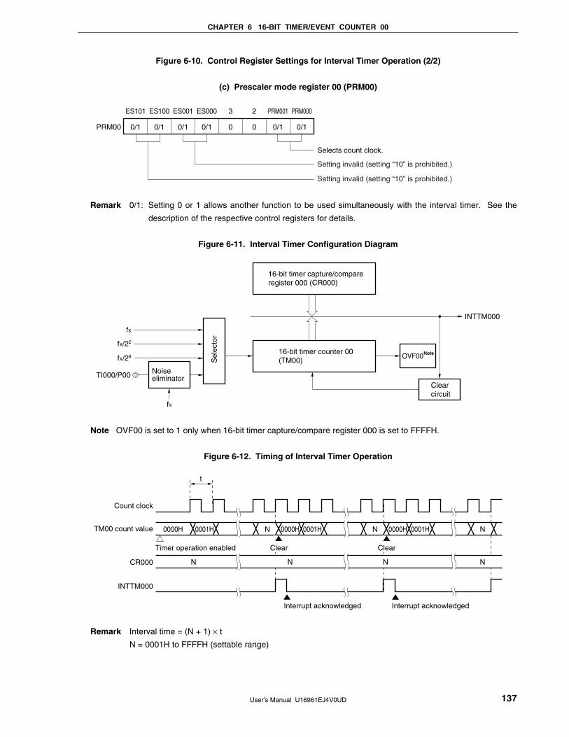
CHAPTER 6 16-BIT TIMER/EVENT COUNTER 00
User’s Manual U16961EJ4V0UD 137
Figure 6-10. Control Register Settings for Interval Timer Operation (2/2)
(c) Prescaler mode register 00 (PRM00)
ES101
0/1
ES100
0/1
ES001
0/1
ES000
0/1
3
0
2
0
PRM001
0/1
PRM000
0/1PRM00
Selects count clock.
Setting invalid (setting “10” is prohibited.)
Setting invalid (setting “10” is prohibited.)
Remark 0/1: Setting 0 or 1 allows another function to be used simultaneously with the interval timer. See the
description of the respective control registers for details.
Figure 6-11. Interval Timer Configuration Diagram
16-bit timer capture/compareregister 000 (CR000)
16-bit timer counter 00(TM00)
OVF00Note
Clearcircuit
INTTM000
fX
fX/22
fX/28
TI000/P00
Sel
ecto
r
Noiseeliminator
fX
Note OVF00 is set to 1 only when 16-bit timer capture/compare register 000 is set to FFFFH.
Figure 6-12. Timing of Interval Timer Operation
Count clock
t
TM00 count value
CR000
INTTM000
0000H 0001H N 0000H 0001H N 0000H 0001H N
NNNN
Timer operation enabled Clear Clear
Interrupt acknowledged Interrupt acknowledged
Remark Interval time = (N + 1) × t
N = 0001H to FFFFH (settable range)
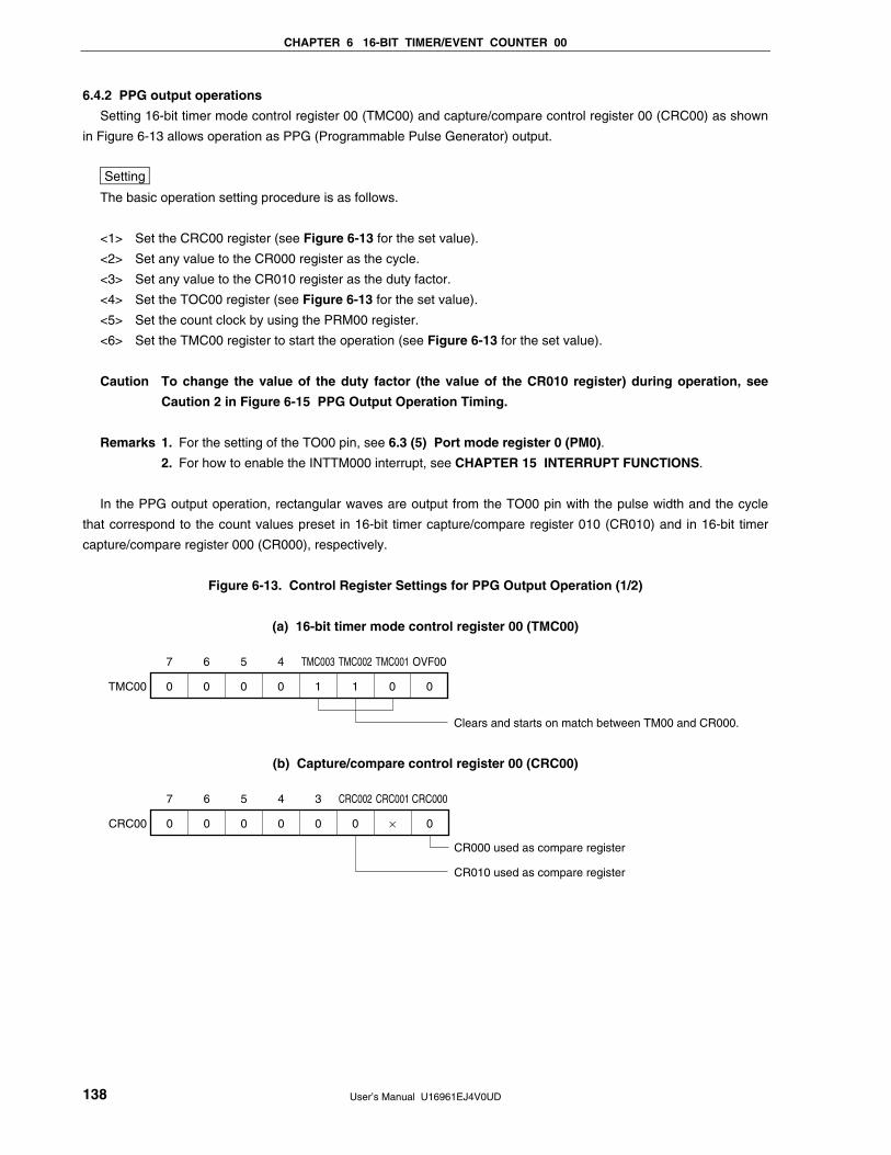
CHAPTER 6 16-BIT TIMER/EVENT COUNTER 00
User’s Manual U16961EJ4V0UD 138
6.4.2 PPG output operations
Setting 16-bit timer mode control register 00 (TMC00) and capture/compare control register 00 (CRC00) as shown
in Figure 6-13 allows operation as PPG (Programmable Pulse Generator) output.
Setting
The basic operation setting procedure is as follows.
<1> Set the CRC00 register (see Figure 6-13 for the set value).
<2> Set any value to the CR000 register as the cycle.
<3> Set any value to the CR010 register as the duty factor.
<4> Set the TOC00 register (see Figure 6-13 for the set value).
<5> Set the count clock by using the PRM00 register.
<6> Set the TMC00 register to start the operation (see Figure 6-13 for the set value).
Caution To change the value of the duty factor (the value of the CR010 register) during operation, see
Caution 2 in Figure 6-15 PPG Output Operation Timing.
Remarks 1. For the setting of the TO00 pin, see 6.3 (5) Port mode register 0 (PM0).
2. For how to enable the INTTM000 interrupt, see CHAPTER 15 INTERRUPT FUNCTIONS.
In the PPG output operation, rectangular waves are output from the TO00 pin with the pulse width and the cycle
that correspond to the count values preset in 16-bit timer capture/compare register 010 (CR010) and in 16-bit timer
capture/compare register 000 (CR000), respectively.
Figure 6-13. Control Register Settings for PPG Output Operation (1/2)
(a) 16-bit timer mode control register 00 (TMC00)
7
0
6
0
5
0
4
0
TMC003
1
TMC002
1
TMC001
0
OVF00
0TMC00
Clears and starts on match between TM00 and CR000.
(b) Capture/compare control register 00 (CRC00)
7
0
6
0
5
0
4
0
3
0
CRC002
0
CRC001
×
CRC000
0CRC00
CR000 used as compare register
CR010 used as compare register
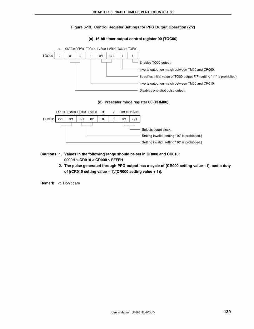
CHAPTER 6 16-BIT TIMER/EVENT COUNTER 00
User’s Manual U16961EJ4V0UD 139
Figure 6-13. Control Register Settings for PPG Output Operation (2/2)
(c) 16-bit timer output control register 00 (TOC00)
7
0
OSPT00
0
OSPE00
0
TOC004
1
LVS00
0/1
LVR00
0/1
TOC001
1
TOE00
1TOC00
Enables TO00 output.
Inverts output on match between TM00 and CR000.
Specifies initial value of TO00 output F/F (setting “11” is prohibited).
Inverts output on match between TM00 and CR010.
Disables one-shot pulse output.
(d) Prescaler mode register 00 (PRM00)
ES101
0/1
ES100
0/1
ES001
0/1
ES000
0/1
3
0
2
0
PRM001
0/1
PRM000
0/1PRM00
Selects count clock.
Setting invalid (setting “10” is prohibited.)
Setting invalid (setting “10” is prohibited.)
Cautions 1. Values in the following range should be set in CR000 and CR010:
0000H ≤ CR010 < CR000 ≤ FFFFH
2. The pulse generated through PPG output has a cycle of [CR000 setting value +1], and a duty
of [(CR010 setting value + 1)/(CR000 setting value + 1)].
Remark ×: Don’t care
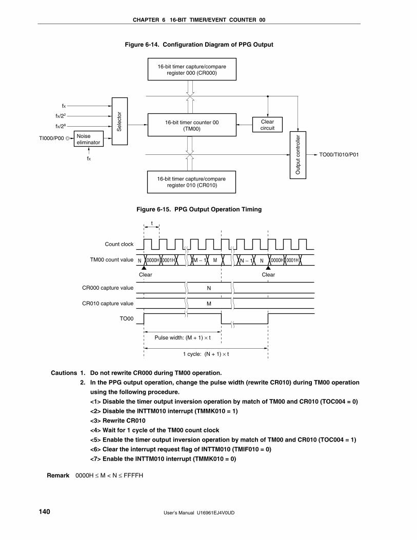
CHAPTER 6 16-BIT TIMER/EVENT COUNTER 00
User’s Manual U16961EJ4V0UD 140
Figure 6-14. Configuration Diagram of PPG Output
16-bit timer capture/compareregister 000 (CR000)
16-bit timer counter 00(TM00)
Clearcircuit
Noise eliminator
fX
fX
fX/22
fX/28
TI000/P00
16-bit timer capture/compare register 010 (CR010)
TO00/TI010/P01
Sel
ecto
r
Out
put c
ontr
olle
r
Figure 6-15. PPG Output Operation Timing
t
0000H 0000H 0001H0001H M − 1
Count clock
TM00 count value
TO00
Pulse width: (M + 1) × t
1 cycle: (N + 1) × t
NCR000 capture value
CR010 capture value M
M N − 1 NN
ClearClear
Cautions 1. Do not rewrite CR000 during TM00 operation.
2. In the PPG output operation, change the pulse width (rewrite CR010) during TM00 operation
using the following procedure.
<1> Disable the timer output inversion operation by match of TM00 and CR010 (TOC004 = 0)
<2> Disable the INTTM010 interrupt (TMMK010 = 1)
<3> Rewrite CR010
<4> Wait for 1 cycle of the TM00 count clock
<5> Enable the timer output inversion operation by match of TM00 and CR010 (TOC004 = 1)
<6> Clear the interrupt request flag of INTTM010 (TMIF010 = 0)
<7> Enable the INTTM010 interrupt (TMMK010 = 0)
Remark 0000H ≤ M < N ≤ FFFFH
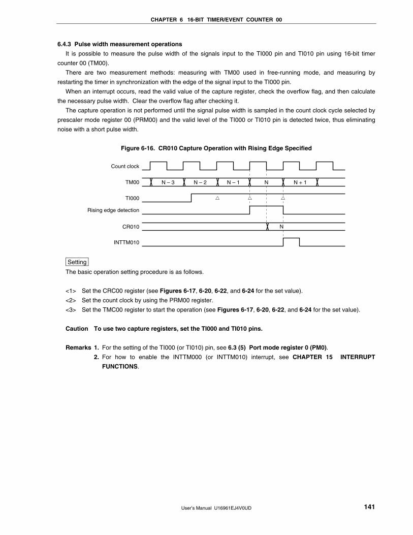
CHAPTER 6 16-BIT TIMER/EVENT COUNTER 00
User’s Manual U16961EJ4V0UD 141
6.4.3 Pulse width measurement operations
It is possible to measure the pulse width of the signals input to the TI000 pin and TI010 pin using 16-bit timer
counter 00 (TM00).
There are two measurement methods: measuring with TM00 used in free-running mode, and measuring by
restarting the timer in synchronization with the edge of the signal input to the TI000 pin.
When an interrupt occurs, read the valid value of the capture register, check the overflow flag, and then calculate
the necessary pulse width. Clear the overflow flag after checking it.
The capture operation is not performed until the signal pulse width is sampled in the count clock cycle selected by
prescaler mode register 00 (PRM00) and the valid level of the TI000 or TI010 pin is detected twice, thus eliminating
noise with a short pulse width.
Figure 6-16. CR010 Capture Operation with Rising Edge Specified
Count clock
TM00
TI000
Rising edge detection
CR010
INTTM010
N – 3 N – 2 N – 1 N N + 1
N
Setting
The basic operation setting procedure is as follows.
<1> Set the CRC00 register (see Figures 6-17, 6-20, 6-22, and 6-24 for the set value).
<2> Set the count clock by using the PRM00 register.
<3> Set the TMC00 register to start the operation (see Figures 6-17, 6-20, 6-22, and 6-24 for the set value).
Caution To use two capture registers, set the TI000 and TI010 pins.
Remarks 1. For the setting of the TI000 (or TI010) pin, see 6.3 (5) Port mode register 0 (PM0).
2. For how to enable the INTTM000 (or INTTM010) interrupt, see CHAPTER 15 INTERRUPT
FUNCTIONS.
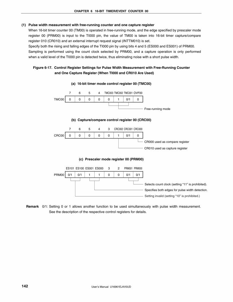
CHAPTER 6 16-BIT TIMER/EVENT COUNTER 00
User’s Manual U16961EJ4V0UD 142
(1) Pulse width measurement with free-running counter and one capture register
When 16-bit timer counter 00 (TM00) is operated in free-running mode, and the edge specified by prescaler mode
register 00 (PRM00) is input to the TI000 pin, the value of TM00 is taken into 16-bit timer capture/compare
register 010 (CR010) and an external interrupt request signal (INTTM010) is set.
Specify both the rising and falling edges of the TI000 pin by using bits 4 and 5 (ES000 and ES001) of PRM00.
Sampling is performed using the count clock selected by PRM00, and a capture operation is only performed
when a valid level of the TI000 pin is detected twice, thus eliminating noise with a short pulse width.
Figure 6-17. Control Register Settings for Pulse Width Measurement with Free-Running Counter
and One Capture Register (When TI000 and CR010 Are Used)
(a) 16-bit timer mode control register 00 (TMC00)
7
0
6
0
5
0
4
0
TMC003
0
TMC002
1
TMC001
0/1
OVF00
0TMC00
Free-running mode
(b) Capture/compare control register 00 (CRC00)
7
0
6
0
5
0
4
0
3
0
CRC002
1
CRC001
0/1
CRC000
0CRC00
CR000 used as compare register
CR010 used as capture register
(c) Prescaler mode register 00 (PRM00)
ES101
0/1
ES100
0/1
ES001
1
ES000
1
3
0
2
0
PRM001
0/1
PRM000
0/1PRM00
Selects count clock (setting “11” is prohibited).
Specifies both edges for pulse width detection.
Setting invalid (setting “10” is prohibited.)
Remark 0/1: Setting 0 or 1 allows another function to be used simultaneously with pulse width measurement.
See the description of the respective control registers for details.
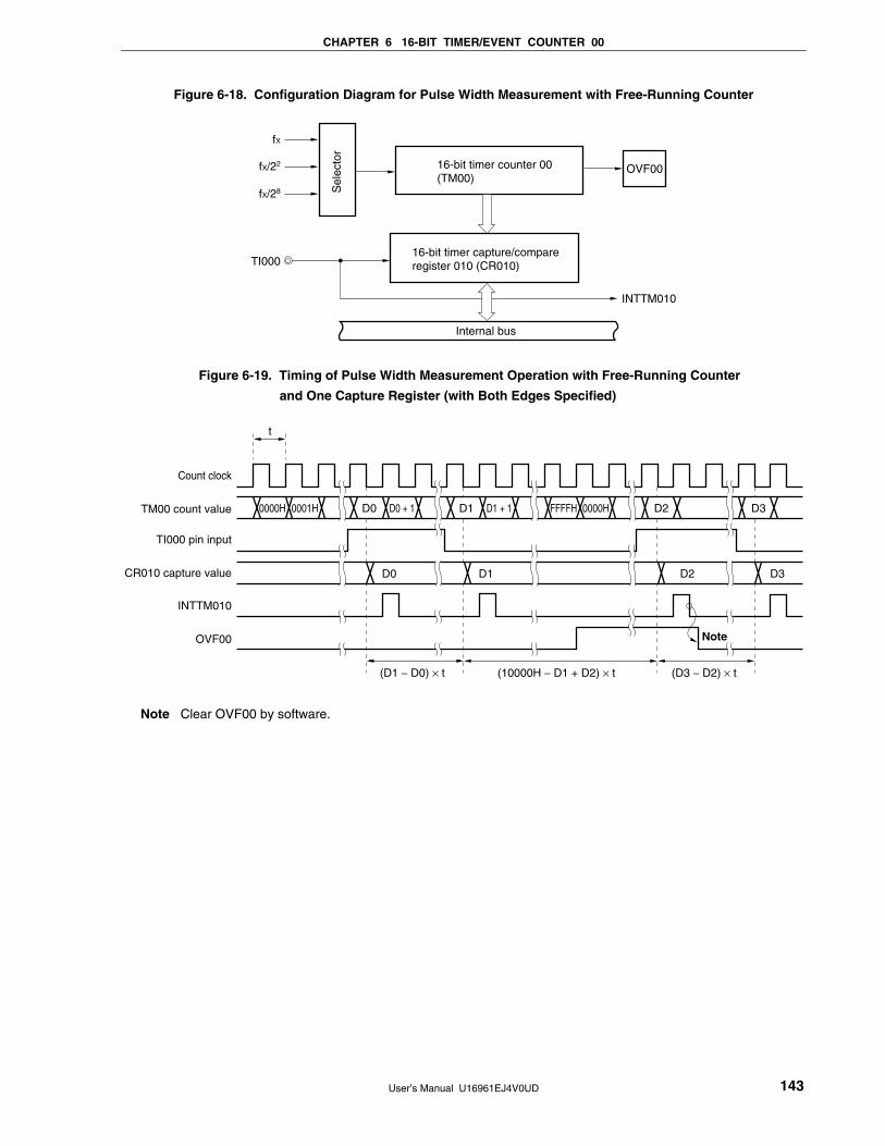
CHAPTER 6 16-BIT TIMER/EVENT COUNTER 00
User’s Manual U16961EJ4V0UD 143
Figure 6-18. Configuration Diagram for Pulse Width Measurement with Free-Running Counter
fX
fX/22
fX/28
TI000
16-bit timer counter 00(TM00)
OVF00
16-bit timer capture/compareregister 010 (CR010)
Internal bus
INTTM010
Sel
ecto
r
Figure 6-19. Timing of Pulse Width Measurement Operation with Free-Running Counter
and One Capture Register (with Both Edges Specified)
t
0000H 0000HFFFFH0001H D0
D0
Count clock
TM00 count value
TI000 pin input
CR010 capture value
INTTM010
OVF00
(D1 − D0) × t (D3 − D2) × t(10000H − D1 + D2) × t
D1 D2 D3
D2 D3D0 + 1 D1 D1 + 1
Note
Note Clear OVF00 by software.
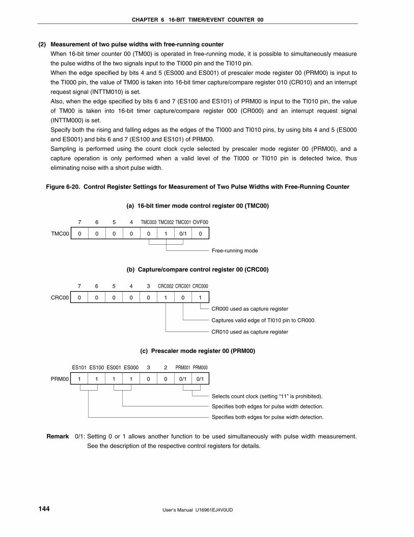
CHAPTER 6 16-BIT TIMER/EVENT COUNTER 00
User’s Manual U16961EJ4V0UD 144
(2) Measurement of two pulse widths with free-running counter
When 16-bit timer counter 00 (TM00) is operated in free-running mode, it is possible to simultaneously measure
the pulse widths of the two signals input to the TI000 pin and the TI010 pin.
When the edge specified by bits 4 and 5 (ES000 and ES001) of prescaler mode register 00 (PRM00) is input to
the TI000 pin, the value of TM00 is taken into 16-bit timer capture/compare register 010 (CR010) and an interrupt
request signal (INTTM010) is set.
Also, when the edge specified by bits 6 and 7 (ES100 and ES101) of PRM00 is input to the TI010 pin, the value
of TM00 is taken into 16-bit timer capture/compare register 000 (CR000) and an interrupt request signal
(INTTM000) is set.
Specify both the rising and falling edges as the edges of the TI000 and TI010 pins, by using bits 4 and 5 (ES000
and ES001) and bits 6 and 7 (ES100 and ES101) of PRM00.
Sampling is performed using the count clock cycle selected by prescaler mode register 00 (PRM00), and a
capture operation is only performed when a valid level of the TI000 or TI010 pin is detected twice, thus
eliminating noise with a short pulse width.
Figure 6-20. Control Register Settings for Measurement of Two Pulse Widths with Free-Running Counter
(a) 16-bit timer mode control register 00 (TMC00)
7
0
6
0
5
0
4
0
TMC003
0
TMC002
1
TMC001
0/1
OVF00
0TMC00
Free-running mode
(b) Capture/compare control register 00 (CRC00)
7
0
6
0
5
0
4
0
3
0
CRC002
1
CRC001
0
CRC000
1CRC00
CR000 used as capture register
Captures valid edge of TI010 pin to CR000.
CR010 used as capture register
(c) Prescaler mode register 00 (PRM00)
ES101
1
ES100
1
ES001
1
ES000
1
3
0
2
0
PRM001
0/1
PRM000
0/1PRM00
Selects count clock (setting “11” is prohibited).
Specifies both edges for pulse width detection.
Specifies both edges for pulse width detection.
Remark 0/1: Setting 0 or 1 allows another function to be used simultaneously with pulse width measurement.
See the description of the respective control registers for details.
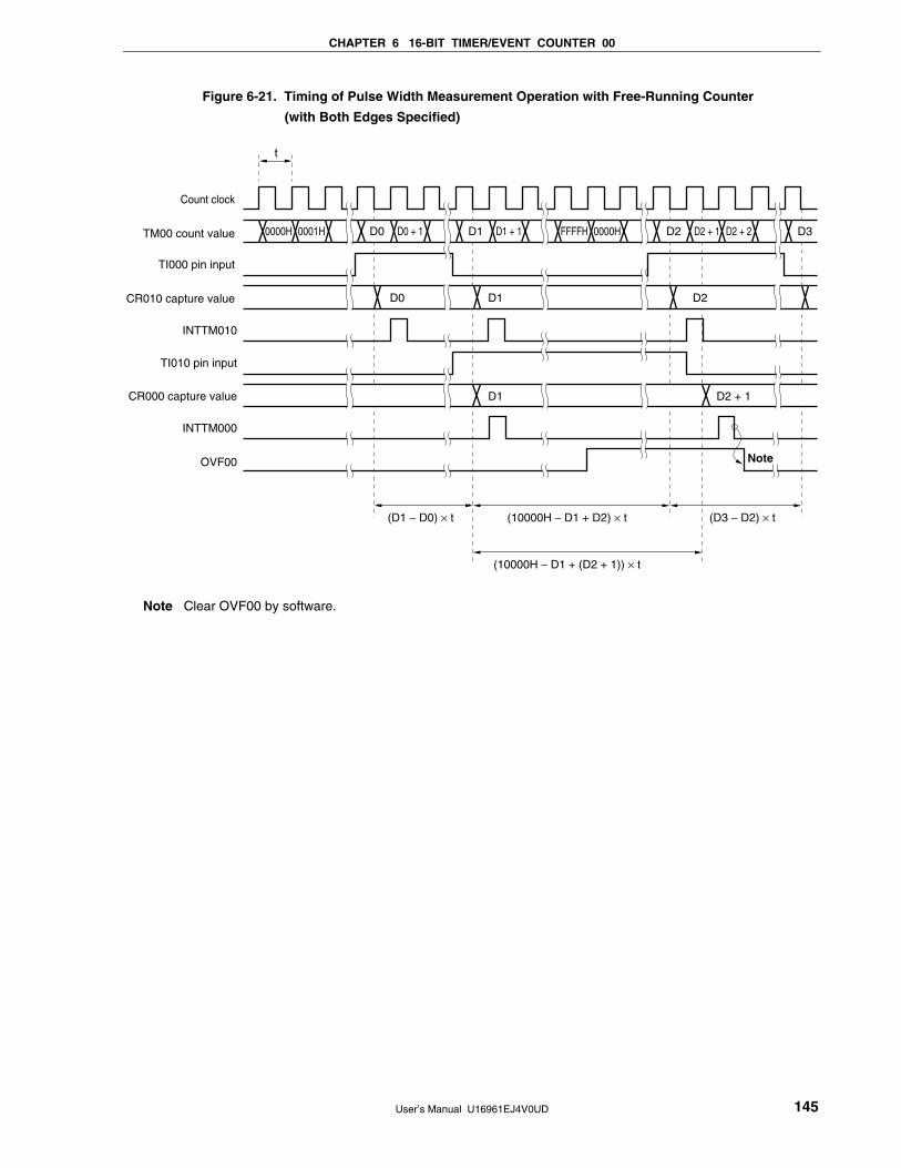
CHAPTER 6 16-BIT TIMER/EVENT COUNTER 00
User’s Manual U16961EJ4V0UD 145
Figure 6-21. Timing of Pulse Width Measurement Operation with Free-Running Counter
(with Both Edges Specified)
t
0000H 0000HFFFFH0001H D0
D0
TI010 pin input
CR000 capture value
INTTM010
INTTM000
OVF00
(D1 − D0) × t (D3 − D2) × t(10000H − D1 + D2) × t
(10000H − D1 + (D2 + 1)) × t
D1
D2 + 1D1
D2
D2 D3D0 + 1 D1 D1 + 1 D2 + 1 D2 + 2
Count clock
TM00 count value
TI000 pin input
CR010 capture value
Note
Note Clear OVF00 by software.
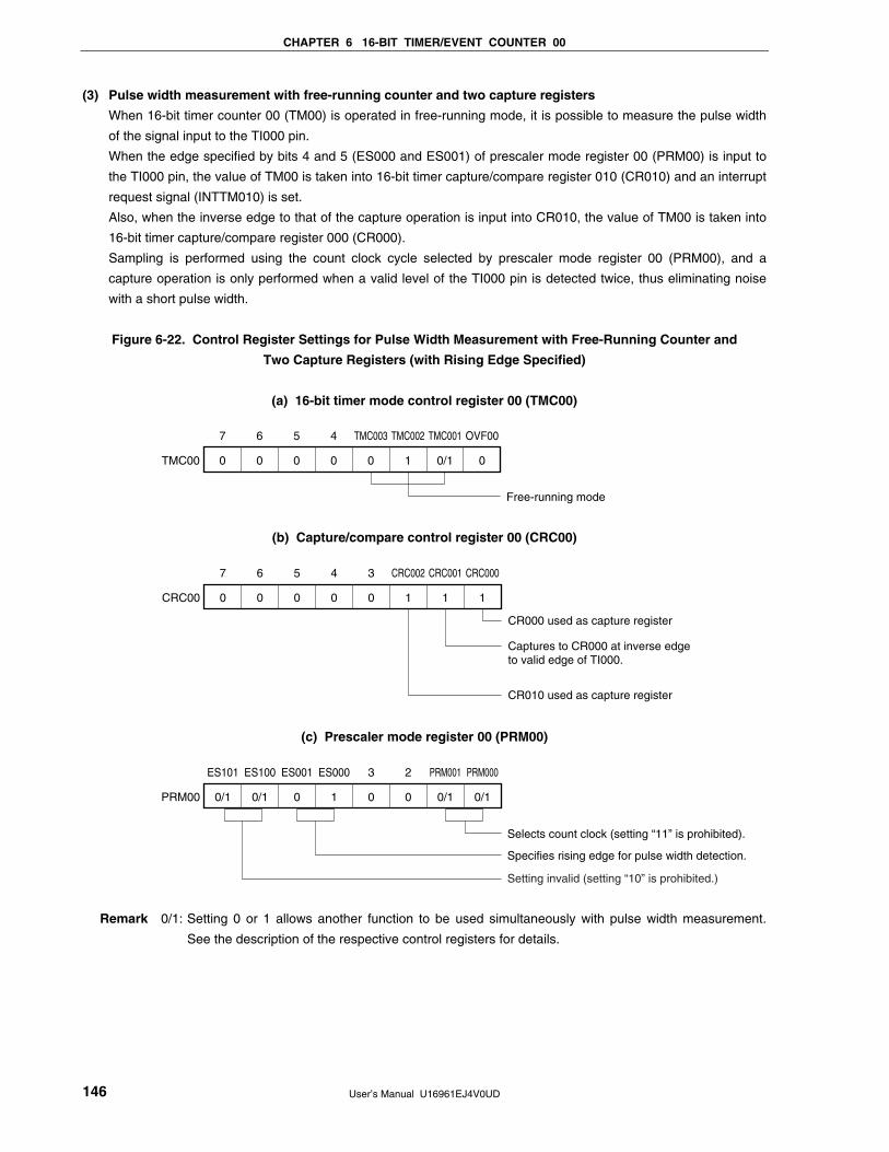
CHAPTER 6 16-BIT TIMER/EVENT COUNTER 00
User’s Manual U16961EJ4V0UD 146
(3) Pulse width measurement with free-running counter and two capture registers
When 16-bit timer counter 00 (TM00) is operated in free-running mode, it is possible to measure the pulse width
of the signal input to the TI000 pin.
When the edge specified by bits 4 and 5 (ES000 and ES001) of prescaler mode register 00 (PRM00) is input to
the TI000 pin, the value of TM00 is taken into 16-bit timer capture/compare register 010 (CR010) and an interrupt
request signal (INTTM010) is set.
Also, when the inverse edge to that of the capture operation is input into CR010, the value of TM00 is taken into
16-bit timer capture/compare register 000 (CR000).
Sampling is performed using the count clock cycle selected by prescaler mode register 00 (PRM00), and a
capture operation is only performed when a valid level of the TI000 pin is detected twice, thus eliminating noise
with a short pulse width.
Figure 6-22. Control Register Settings for Pulse Width Measurement with Free-Running Counter and
Two Capture Registers (with Rising Edge Specified)
(a) 16-bit timer mode control register 00 (TMC00)
7
0
6
0
5
0
4
0
TMC003
0
TMC002
1
TMC001
0/1
OVF00
0TMC00
Free-running mode
(b) Capture/compare control register 00 (CRC00)
7
0
6
0
5
0
4
0
3
0
CRC002
1
CRC001
1
CRC000
1CRC00
CR000 used as capture register
Captures to CR000 at inverse edge to valid edge of TI000.
CR010 used as capture register
(c) Prescaler mode register 00 (PRM00)
ES101
0/1
ES100
0/1
ES001
0
ES000
1
3
0
2
0
PRM001
0/1
PRM000
0/1PRM00
Selects count clock (setting “11” is prohibited).
Specifies rising edge for pulse width detection.
Setting invalid (setting “10” is prohibited.)
Remark 0/1: Setting 0 or 1 allows another function to be used simultaneously with pulse width measurement.
See the description of the respective control registers for details.
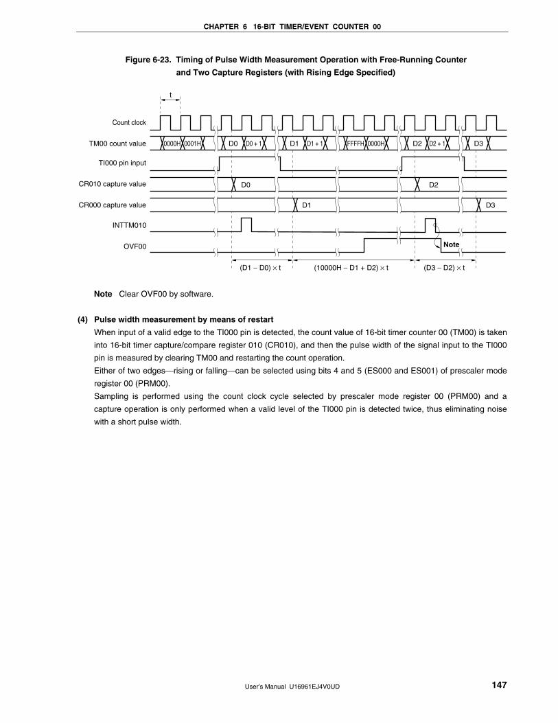
CHAPTER 6 16-BIT TIMER/EVENT COUNTER 00
User’s Manual U16961EJ4V0UD 147
Figure 6-23. Timing of Pulse Width Measurement Operation with Free-Running Counter
and Two Capture Registers (with Rising Edge Specified)
t
0000H 0000HFFFFH0001H D0
D0
INTTM010
OVF00
D2
D1 D3
D2 D3D0 + 1 D2 + 1D1 D1 + 1
CR000 capture value
Count clock
TM00 count value
TI000 pin input
CR010 capture value
(D1 − D0) × t (D3 − D2) × t(10000H − D1 + D2) × t
Note
Note Clear OVF00 by software.
(4) Pulse width measurement by means of restart
When input of a valid edge to the TI000 pin is detected, the count value of 16-bit timer counter 00 (TM00) is taken
into 16-bit timer capture/compare register 010 (CR010), and then the pulse width of the signal input to the TI000
pin is measured by clearing TM00 and restarting the count operation.
Either of two edgesrising or fallingcan be selected using bits 4 and 5 (ES000 and ES001) of prescaler mode
register 00 (PRM00).
Sampling is performed using the count clock cycle selected by prescaler mode register 00 (PRM00) and a
capture operation is only performed when a valid level of the TI000 pin is detected twice, thus eliminating noise
with a short pulse width.
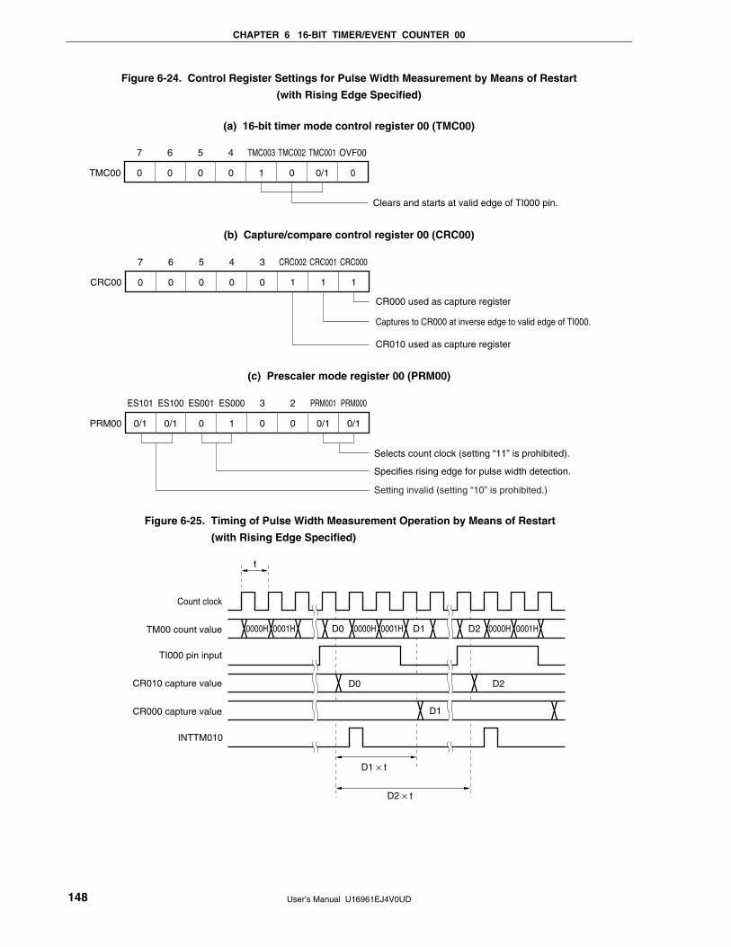
CHAPTER 6 16-BIT TIMER/EVENT COUNTER 00
User’s Manual U16961EJ4V0UD 148
Figure 6-24. Control Register Settings for Pulse Width Measurement by Means of Restart
(with Rising Edge Specified)
(a) 16-bit timer mode control register 00 (TMC00)
7
0
6
0
5
0
4
0
TMC003
1
TMC002
0
TMC001
0/1
OVF00
0TMC00
Clears and starts at valid edge of TI000 pin.
(b) Capture/compare control register 00 (CRC00)
7
0
6
0
5
0
4
0
3
0
CRC002
1
CRC001
1
CRC000
1CRC00
CR000 used as capture register
Captures to CR000 at inverse edge to valid edge of TI000.
CR010 used as capture register
(c) Prescaler mode register 00 (PRM00)
ES101
0/1
ES100
0/1
ES001
0
ES000
1
3
0
2
0
PRM001
0/1
PRM000
0/1PRM00
Selects count clock (setting “11” is prohibited).
Specifies rising edge for pulse width detection.
Setting invalid (setting “10” is prohibited.)
Figure 6-25. Timing of Pulse Width Measurement Operation by Means of Restart
(with Rising Edge Specified)
t
0000H 0001H0000H0001H 0000H 0001HD0
D0
INTTM010
D1 × t
D2 × t
D2
D1
D2D1
CR000 capture value
Count clock
TM00 count value
TI000 pin input
CR010 capture value
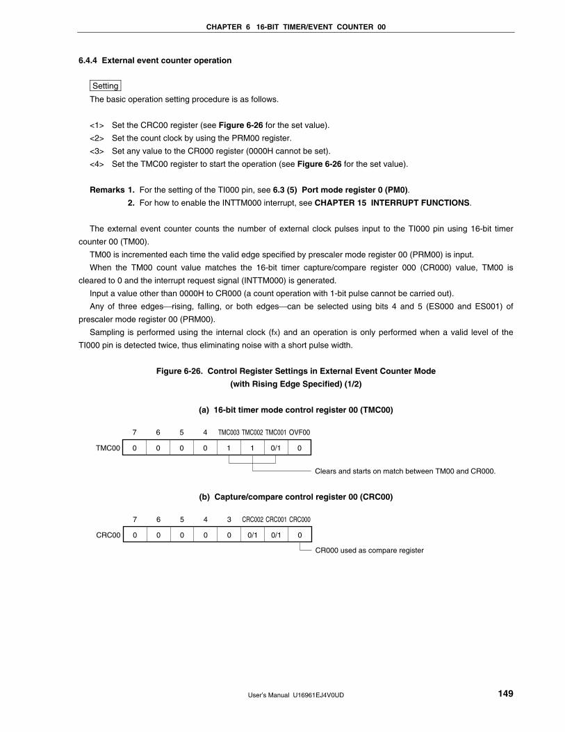
CHAPTER 6 16-BIT TIMER/EVENT COUNTER 00
User’s Manual U16961EJ4V0UD 149
6.4.4 External event counter operation
Setting
The basic operation setting procedure is as follows.
<1> Set the CRC00 register (see Figure 6-26 for the set value).
<2> Set the count clock by using the PRM00 register.
<3> Set any value to the CR000 register (0000H cannot be set).
<4> Set the TMC00 register to start the operation (see Figure 6-26 for the set value).
Remarks 1. For the setting of the TI000 pin, see 6.3 (5) Port mode register 0 (PM0).
2. For how to enable the INTTM000 interrupt, see CHAPTER 15 INTERRUPT FUNCTIONS.
The external event counter counts the number of external clock pulses input to the TI000 pin using 16-bit timer
counter 00 (TM00).
TM00 is incremented each time the valid edge specified by prescaler mode register 00 (PRM00) is input.
When the TM00 count value matches the 16-bit timer capture/compare register 000 (CR000) value, TM00 is
cleared to 0 and the interrupt request signal (INTTM000) is generated.
Input a value other than 0000H to CR000 (a count operation with 1-bit pulse cannot be carried out).
Any of three edgesrising, falling, or both edgescan be selected using bits 4 and 5 (ES000 and ES001) of
prescaler mode register 00 (PRM00).
Sampling is performed using the internal clock (fX) and an operation is only performed when a valid level of the
TI000 pin is detected twice, thus eliminating noise with a short pulse width.
Figure 6-26. Control Register Settings in External Event Counter Mode
(with Rising Edge Specified) (1/2)
(a) 16-bit timer mode control register 00 (TMC00)
7
0
6
0
5
0
4
0
TMC003
1
TMC002
1
TMC001
0/1
OVF00
0TMC00
Clears and starts on match between TM00 and CR000.
(b) Capture/compare control register 00 (CRC00)
7
0
6
0
5
0
4
0
3
0
CRC002
0/1
CRC001
0/1
CRC000
0CRC00
CR000 used as compare register
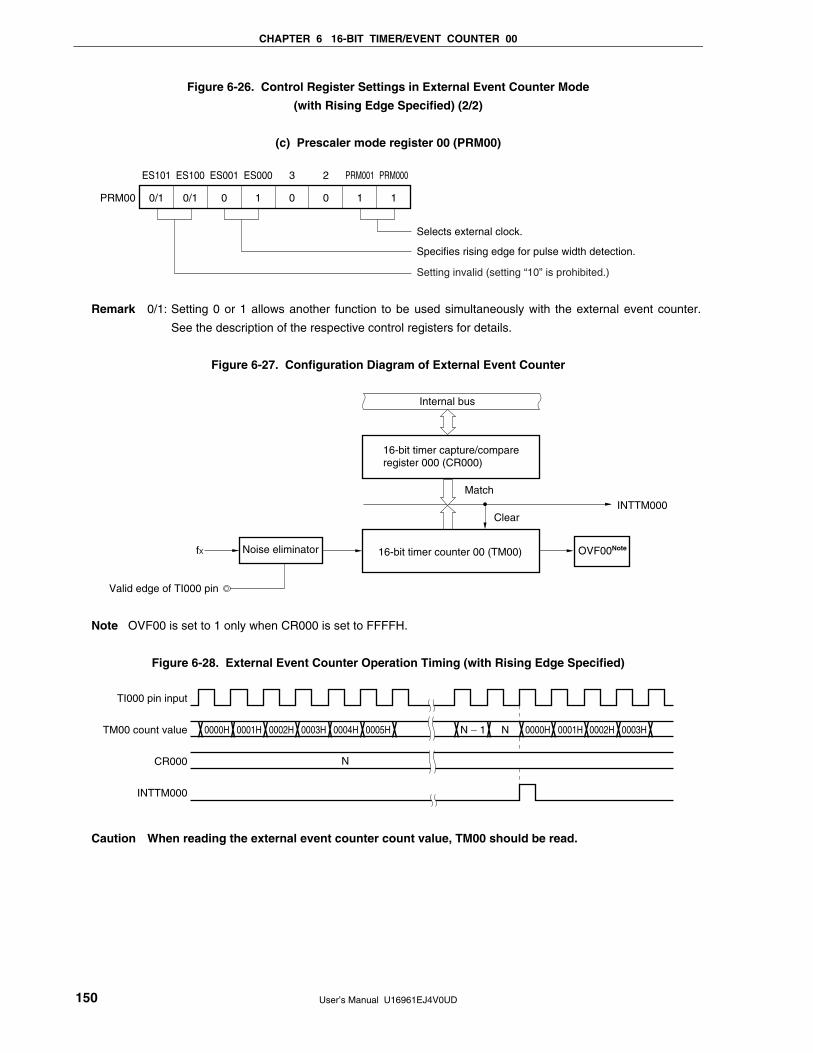
CHAPTER 6 16-BIT TIMER/EVENT COUNTER 00
User’s Manual U16961EJ4V0UD 150
Figure 6-26. Control Register Settings in External Event Counter Mode
(with Rising Edge Specified) (2/2)
(c) Prescaler mode register 00 (PRM00)
ES101
0/1
ES100
0/1
ES001
0
ES000
1
3
0
2
0
PRM001
1
PRM000
1PRM00
Selects external clock.
Specifies rising edge for pulse width detection.
Setting invalid (setting “10” is prohibited.)
Remark 0/1: Setting 0 or 1 allows another function to be used simultaneously with the external event counter.
See the description of the respective control registers for details.
Figure 6-27. Configuration Diagram of External Event Counter
fX
Internal bus
16-bit timer capture/compare register 000 (CR000)
Match
Clear
OVF00NoteNoise eliminator 16-bit timer counter 00 (TM00)
Valid edge of TI000 pin
INTTM000
Note OVF00 is set to 1 only when CR000 is set to FFFFH.
Figure 6-28. External Event Counter Operation Timing (with Rising Edge Specified)
TI000 pin input
TM00 count value
CR000
INTTM000
0000H 0001H 0002H 0003H 0004H 0005H N − 1 N 0000H 0001H 0002H 0003H
N
Caution When reading the external event counter count value, TM00 should be read.
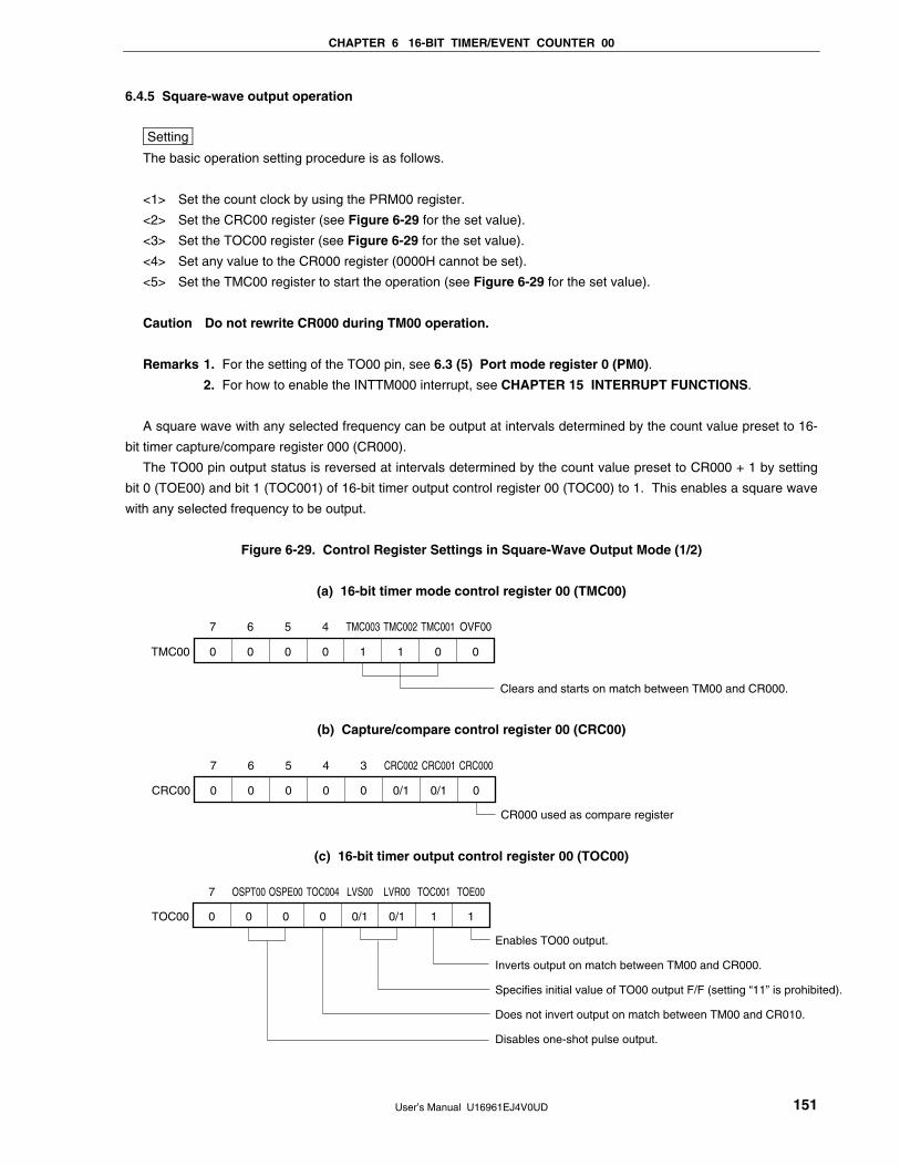
CHAPTER 6 16-BIT TIMER/EVENT COUNTER 00
User’s Manual U16961EJ4V0UD 151
6.4.5 Square-wave output operation
Setting
The basic operation setting procedure is as follows.
<1> Set the count clock by using the PRM00 register.
<2> Set the CRC00 register (see Figure 6-29 for the set value).
<3> Set the TOC00 register (see Figure 6-29 for the set value).
<4> Set any value to the CR000 register (0000H cannot be set).
<5> Set the TMC00 register to start the operation (see Figure 6-29 for the set value).
Caution Do not rewrite CR000 during TM00 operation.
Remarks 1. For the setting of the TO00 pin, see 6.3 (5) Port mode register 0 (PM0).
2. For how to enable the INTTM000 interrupt, see CHAPTER 15 INTERRUPT FUNCTIONS.
A square wave with any selected frequency can be output at intervals determined by the count value preset to 16-
bit timer capture/compare register 000 (CR000).
The TO00 pin output status is reversed at intervals determined by the count value preset to CR000 + 1 by setting
bit 0 (TOE00) and bit 1 (TOC001) of 16-bit timer output control register 00 (TOC00) to 1. This enables a square wave
with any selected frequency to be output.
Figure 6-29. Control Register Settings in Square-Wave Output Mode (1/2)
(a) 16-bit timer mode control register 00 (TMC00)
7
0
6
0
5
0
4
0
TMC003
1
TMC002
1
TMC001
0
OVF00
0TMC00
Clears and starts on match between TM00 and CR000.
(b) Capture/compare control register 00 (CRC00)
7
0
6
0
5
0
4
0
3
0
CRC002
0/1
CRC001
0/1
CRC000
0CRC00
CR000 used as compare register
(c) 16-bit timer output control register 00 (TOC00)
7
0
OSPT00
0
OSPE00
0
TOC004
0
LVS00
0/1
LVR00
0/1
TOC001
1
TOE00
1TOC00
Enables TO00 output.
Inverts output on match between TM00 and CR000.
Specifies initial value of TO00 output F/F (setting “11” is prohibited).
Does not invert output on match between TM00 and CR010.
Disables one-shot pulse output.
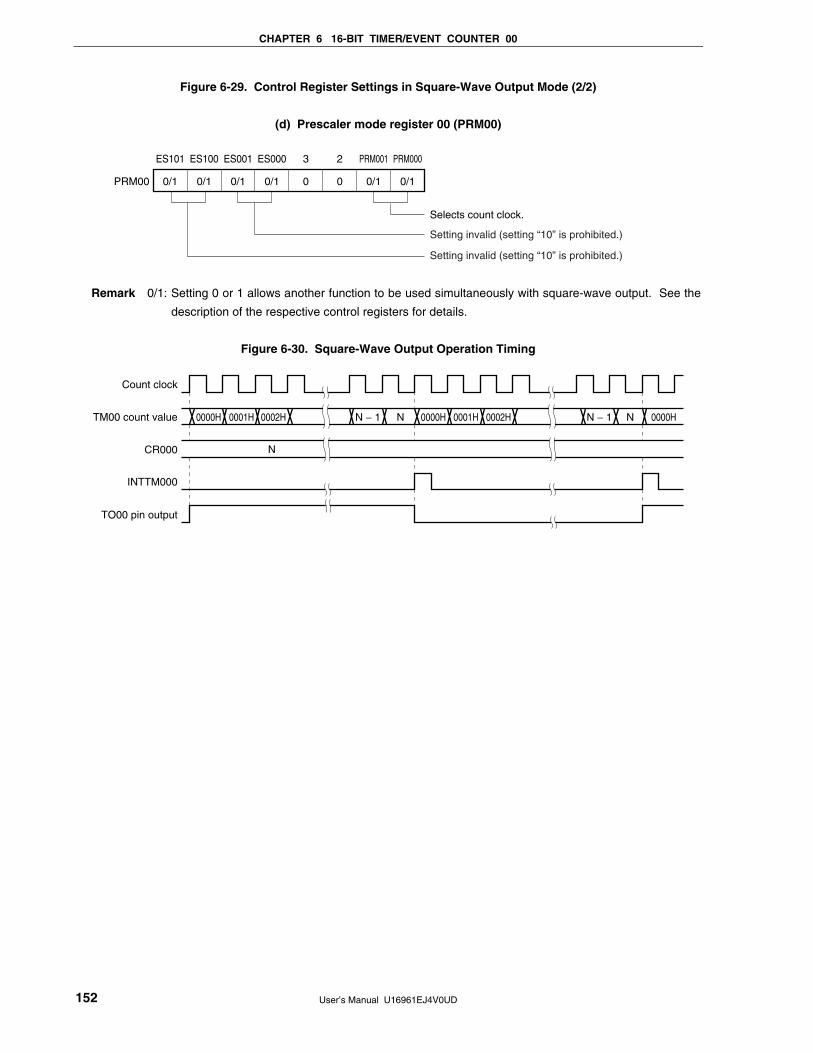
CHAPTER 6 16-BIT TIMER/EVENT COUNTER 00
User’s Manual U16961EJ4V0UD 152
Figure 6-29. Control Register Settings in Square-Wave Output Mode (2/2)
(d) Prescaler mode register 00 (PRM00)
ES101
0/1
ES100
0/1
ES001
0/1
ES000
0/1
3
0
2
0
PRM001
0/1
PRM000
0/1PRM00
Selects count clock.
Setting invalid (setting “10” is prohibited.)
Setting invalid (setting “10” is prohibited.)
Remark 0/1: Setting 0 or 1 allows another function to be used simultaneously with square-wave output. See the
description of the respective control registers for details.
Figure 6-30. Square-Wave Output Operation Timing
Count clock
TM00 count value
CR000
INTTM000
TO00 pin output
0000H 0001H 0002H N − 1 N 0000H 0001H 0002H N − 1 N 0000H
N
CHAPTER 6 16-BIT TIMER/EVENT COUNTER 00
User’s Manual U16961EJ4V0UD 153
6.4.6 One-shot pulse output operation
16-bit timer/event counter 00 can output a one-shot pulse in synchronization with a software trigger or an external
trigger (TI000 pin input).
Setting
The basic operation setting procedure is as follows.
<1> Set the count clock by using the PRM00 register.
<2> Set the CRC00 register (see Figures 6-31 and 6-33 for the set value).
<3> Set the TOC00 register (see Figures 6-31 and 6-33 for the set value).
<4> Set any value to the CR000 and CR010 registers (0000H cannot be set).
<5> Set the TMC00 register to start the operation (see Figures 6-31 and 6-33 for the set value).
Remarks 1. For the setting of the TO00 pin, see 6.3 (5) Port mode register 0 (PM0).
2. For how to enable the INTTM000 (if necessary, INTTM010) interrupt, see CHAPTER 15
INTERRUPT FUNCTIONS.
(1) One-shot pulse output with software trigger
A one-shot pulse can be output from the TO00 pin by setting 16-bit timer mode control register 00 (TMC00),
capture/compare control register 00 (CRC00), and 16-bit timer output control register 00 (TOC00) as shown in
Figure 6-31, and by setting bit 6 (OSPT00) of the TOC00 register to 1 by software.
By setting the OSPT00 bit to 1, 16-bit timer/event counter 00 is cleared and started, and its output becomes
active at the count value (N) set in advance to 16-bit timer capture/compare register 010 (CR010). After that, the
output becomes inactive at the count value (M) set in advance to 16-bit timer capture/compare register 000
(CR000)Note.
Even after the one-shot pulse has been output, the TM00 register continues its operation. To stop the TM00
register, the TMC003 and TMC002 bits of the TMC00 register must be cleared to 00.
Note The case where N < M is described here. When N > M, the output becomes active with the CR000
register and inactive with the CR010 register. Do not set N to M.
Cautions 1. Do not set the OSPT00 bit to 1 while the one-shot pulse is being output. To output the one-
shot pulse again, wait until the current one-shot pulse output is completed.
2. When using the one-shot pulse output of 16-bit timer/event counter 00 with a software
trigger, do not change the level of the TI000 pin or its alternate-function port pin.
Because the external trigger is valid even in this case, the timer is cleared and started even
at the level of the TI000 pin or its alternate-function port pin, resulting in the output of a
pulse at an undesired timing.
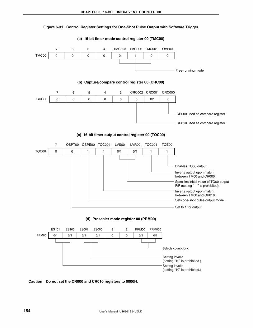
CHAPTER 6 16-BIT TIMER/EVENT COUNTER 00
User’s Manual U16961EJ4V0UD 154
Figure 6-31. Control Register Settings for One-Shot Pulse Output with Software Trigger
(a) 16-bit timer mode control register 00 (TMC00)
0 0 0 0 0
TMC003
TMC00
TMC002 TMC001 OVF007 6 5 4
Free-running mode
1 0 0
(b) Capture/compare control register 00 (CRC00)
0 0 0 0 0
7 6 5 4 3
CRC00
CRC002 CRC001 CRC000
CR000 used as compare register
CR010 used as compare register
0 0/1 0
(c) 16-bit timer output control register 00 (TOC00)
0 0 1 1 0/1TOC00
LVR00LVS00TOC004OSPE00OSPT007 TOC001 TOE00
Enables TO00 output.
Inverts output upon match between TM00 and CR000.
Specifies initial value of TO00 output F/F (setting “11” is prohibited).
Inverts output upon match between TM00 and CR010.
Sets one-shot pulse output mode.
Set to 1 for output.
0/1 1 1
(d) Prescaler mode register 00 (PRM00)
0/1 0/1 0/1 0/1 0 PRM00
PRM001 PRM000
Selects count clock.
Setting invalid (setting “10” is prohibited.)
0 0/1 0/1
ES101 ES100 ES001 ES000
Setting invalid (setting “10” is prohibited.)
3 2
Caution Do not set the CR000 and CR010 registers to 0000H.
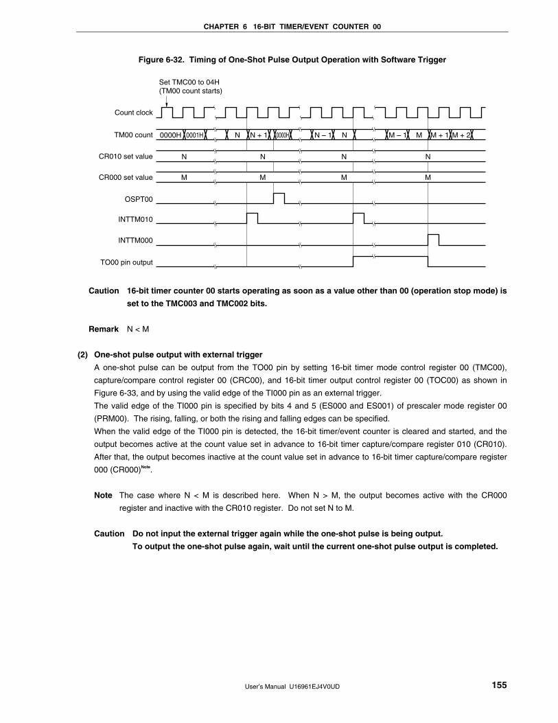
CHAPTER 6 16-BIT TIMER/EVENT COUNTER 00
User’s Manual U16961EJ4V0UD 155
Figure 6-32. Timing of One-Shot Pulse Output Operation with Software Trigger
0000H N
N N N N
M M M M
N MN + 1 N – 1 M – 10001H M + 1 M + 20000H
Count clock
TM00 count
CR010 set value
CR000 set value
OSPT00
INTTM010
INTTM000
TO00 pin output
Set TMC00 to 04H(TM00 count starts)
Caution 16-bit timer counter 00 starts operating as soon as a value other than 00 (operation stop mode) is
set to the TMC003 and TMC002 bits.
Remark N < M
(2) One-shot pulse output with external trigger
A one-shot pulse can be output from the TO00 pin by setting 16-bit timer mode control register 00 (TMC00),
capture/compare control register 00 (CRC00), and 16-bit timer output control register 00 (TOC00) as shown in
Figure 6-33, and by using the valid edge of the TI000 pin as an external trigger.
The valid edge of the TI000 pin is specified by bits 4 and 5 (ES000 and ES001) of prescaler mode register 00
(PRM00). The rising, falling, or both the rising and falling edges can be specified.
When the valid edge of the TI000 pin is detected, the 16-bit timer/event counter is cleared and started, and the
output becomes active at the count value set in advance to 16-bit timer capture/compare register 010 (CR010).
After that, the output becomes inactive at the count value set in advance to 16-bit timer capture/compare register
000 (CR000)Note.
Note The case where N < M is described here. When N > M, the output becomes active with the CR000
register and inactive with the CR010 register. Do not set N to M.
Caution Do not input the external trigger again while the one-shot pulse is being output.
To output the one-shot pulse again, wait until the current one-shot pulse output is completed.
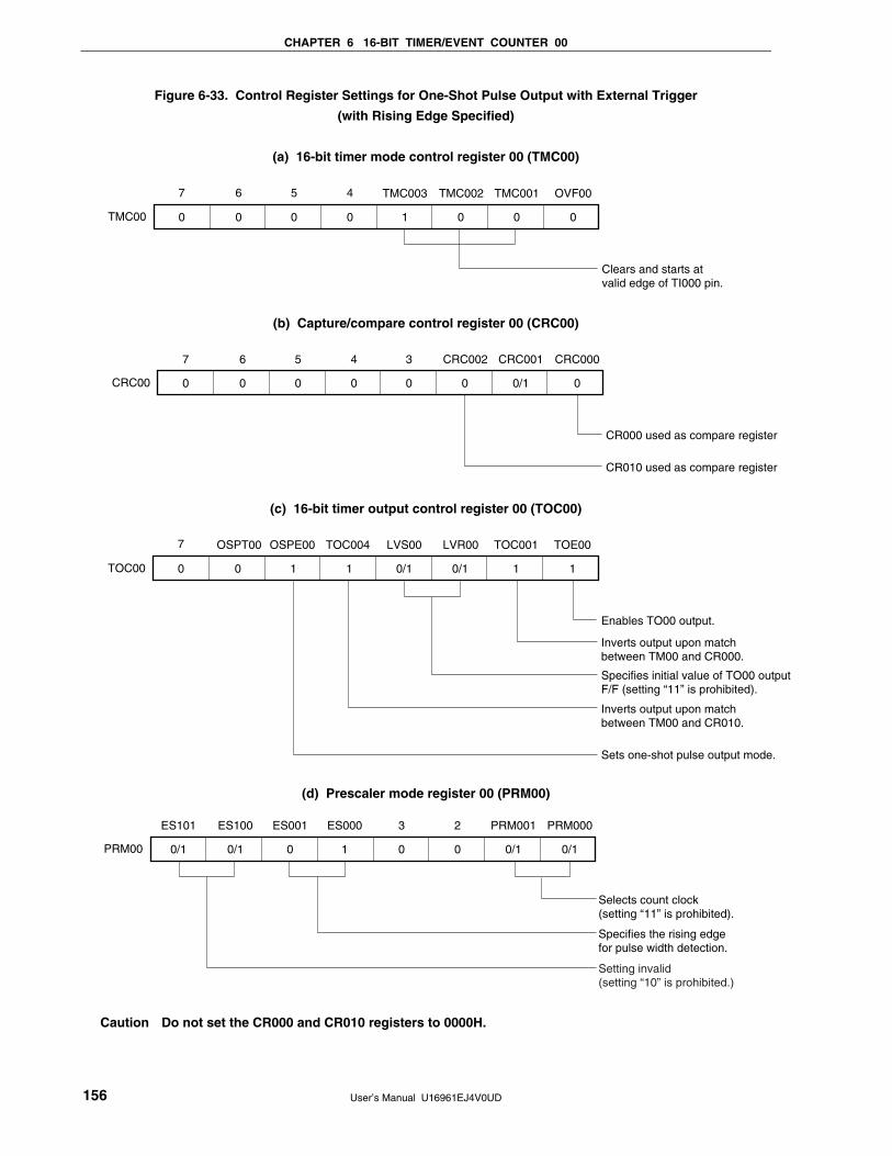
CHAPTER 6 16-BIT TIMER/EVENT COUNTER 00
User’s Manual U16961EJ4V0UD 156
Figure 6-33. Control Register Settings for One-Shot Pulse Output with External Trigger
(with Rising Edge Specified)
(a) 16-bit timer mode control register 00 (TMC00)
0 0 0 0
7 6 5 4
1
TMC003
TMC00
TMC002 TMC001 OVF00
Clears and starts at valid edge of TI000 pin.
0 0 0
(b) Capture/compare control register 00 (CRC00)
0 0 0 0 0
7 6 5 4 3
CRC00
CRC002 CRC001 CRC000
CR000 used as compare register
CR010 used as compare register
0 0/1 0
(c) 16-bit timer output control register 00 (TOC00)
0
7
0 11 0/1TOC00
LVR00 TOC001 TOE00OSPE00OSPT00 TOC004 LVS00
Enables TO00 output.
Inverts output upon match between TM00 and CR000.
Specifies initial value of TO00 output F/F (setting “11” is prohibited).
Inverts output upon match between TM00 and CR010.
Sets one-shot pulse output mode.
0/1 1 1
(d) Prescaler mode register 00 (PRM00)
0/1 0/1 0 1 PRM00
PRM001 PRM000
Selects count clock(setting “11” is prohibited).
Specifies the rising edge for pulse width detection.
0/1 0/1
ES101 ES100 ES001 ES000
Setting invalid (setting “10” is prohibited.)
0 0
3 2
Caution Do not set the CR000 and CR010 registers to 0000H.
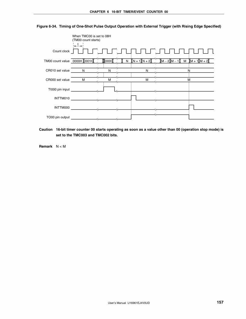
CHAPTER 6 16-BIT TIMER/EVENT COUNTER 00
User’s Manual U16961EJ4V0UD 157
Figure 6-34. Timing of One-Shot Pulse Output Operation with External Trigger (with Rising Edge Specified)
0000H N
N N N N
M M M M
MN + 1 N + 2 M + 1 M + 2M − 2 M − 10001H 0000H
Count clock
TM00 count value
CR010 set value
CR000 set value
TI000 pin input
INTTM010
INTTM000
TO00 pin output
When TMC00 is set to 08H(TM00 count starts)
t
Caution 16-bit timer counter 00 starts operating as soon as a value other than 00 (operation stop mode) is
set to the TMC003 and TMC002 bits.
Remark N < M
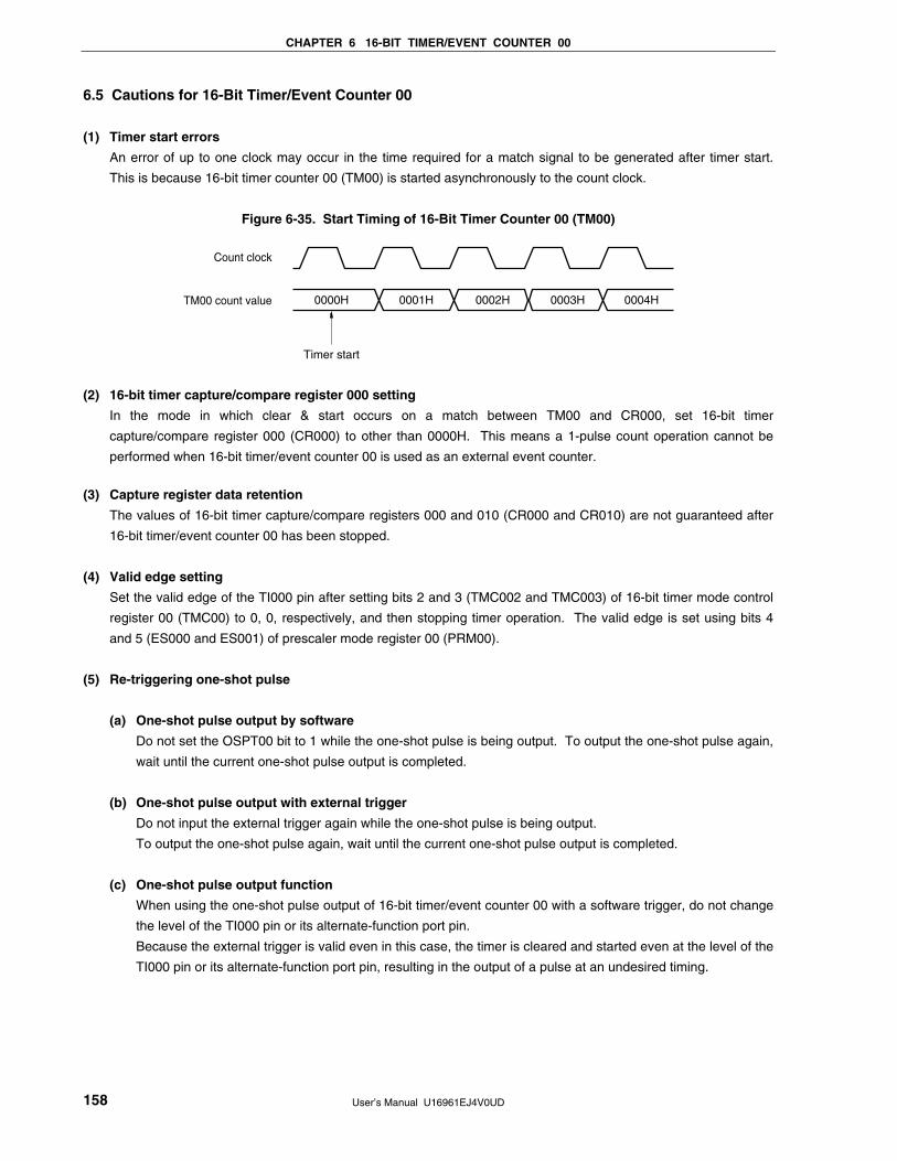
CHAPTER 6 16-BIT TIMER/EVENT COUNTER 00
User’s Manual U16961EJ4V0UD 158
6.5 Cautions for 16-Bit Timer/Event Counter 00
(1) Timer start errors
An error of up to one clock may occur in the time required for a match signal to be generated after timer start.
This is because 16-bit timer counter 00 (TM00) is started asynchronously to the count clock.
Figure 6-35. Start Timing of 16-Bit Timer Counter 00 (TM00)
TM00 count value 0000H 0001H 0002H 0004H
Count clock
Timer start
0003H
(2) 16-bit timer capture/compare register 000 setting
In the mode in which clear & start occurs on a match between TM00 and CR000, set 16-bit timer
capture/compare register 000 (CR000) to other than 0000H. This means a 1-pulse count operation cannot be
performed when 16-bit timer/event counter 00 is used as an external event counter.
(3) Capture register data retention
The values of 16-bit timer capture/compare registers 000 and 010 (CR000 and CR010) are not guaranteed after
16-bit timer/event counter 00 has been stopped.
(4) Valid edge setting
Set the valid edge of the TI000 pin after setting bits 2 and 3 (TMC002 and TMC003) of 16-bit timer mode control
register 00 (TMC00) to 0, 0, respectively, and then stopping timer operation. The valid edge is set using bits 4
and 5 (ES000 and ES001) of prescaler mode register 00 (PRM00).
(5) Re-triggering one-shot pulse
(a) One-shot pulse output by software
Do not set the OSPT00 bit to 1 while the one-shot pulse is being output. To output the one-shot pulse again,
wait until the current one-shot pulse output is completed.
(b) One-shot pulse output with external trigger
Do not input the external trigger again while the one-shot pulse is being output.
To output the one-shot pulse again, wait until the current one-shot pulse output is completed.
(c) One-shot pulse output function
When using the one-shot pulse output of 16-bit timer/event counter 00 with a software trigger, do not change
the level of the TI000 pin or its alternate-function port pin.
Because the external trigger is valid even in this case, the timer is cleared and started even at the level of the
TI000 pin or its alternate-function port pin, resulting in the output of a pulse at an undesired timing.
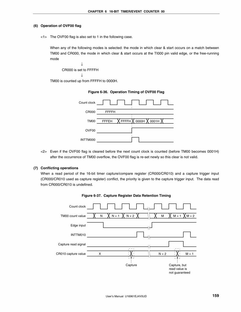
CHAPTER 6 16-BIT TIMER/EVENT COUNTER 00
User’s Manual U16961EJ4V0UD 159
(6) Operation of OVF00 flag
<1> The OVF00 flag is also set to 1 in the following case.
When any of the following modes is selected: the mode in which clear & start occurs on a match between
TM00 and CR000, the mode in which clear & start occurs at the TI000 pin valid edge, or the free-running
mode
↓
CR000 is set to FFFFH
↓
TM00 is counted up from FFFFH to 0000H.
Figure 6-36. Operation Timing of OVF00 Flag
Count clock
CR000
TM00
OVF00
INTTM000
FFFFH
FFFEH FFFFH 0000H 0001H
<2> Even if the OVF00 flag is cleared before the next count clock is counted (before TM00 becomes 0001H)
after the occurrence of TM00 overflow, the OVF00 flag is re-set newly so this clear is not valid.
(7) Conflicting operations
When a read period of the 16-bit timer capture/compare register (CR000/CR010) and a capture trigger input
(CR000/CR010 used as capture register) conflict, the priority is given to the capture trigger input. The data read
from CR000/CR010 is undefined.
Figure 6-37. Capture Register Data Retention Timing
Count clock
TM00 count value
Edge input
INTTM010
Capture read signal
CR010 capture value
N N + 1 N + 2 M M + 1 M + 2
X N + 2
Capture, butread value is not guaranteed
Capture
M + 1
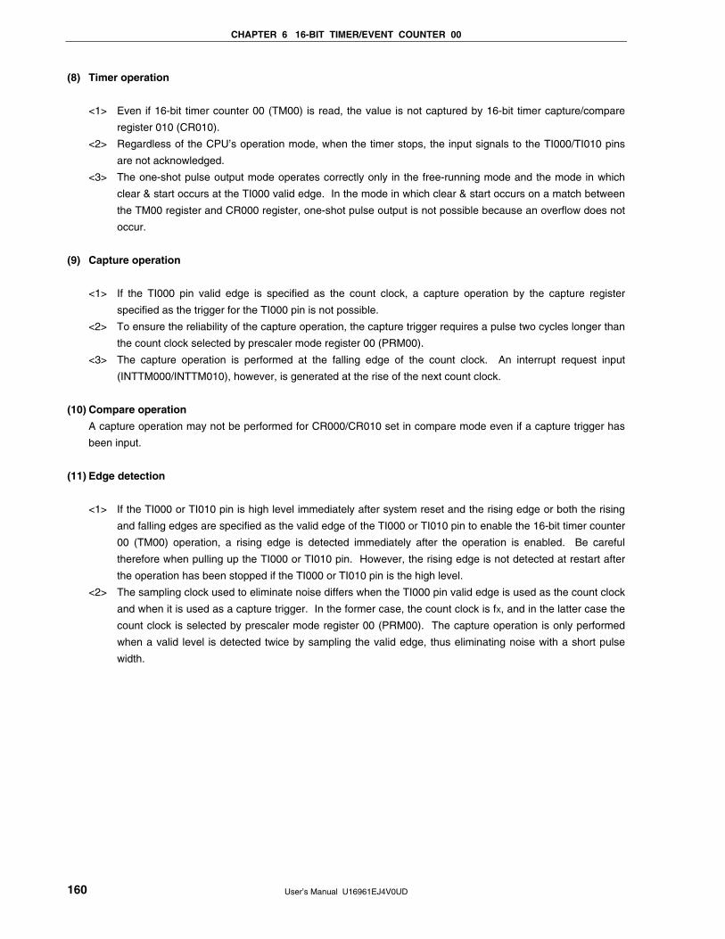
CHAPTER 6 16-BIT TIMER/EVENT COUNTER 00
User’s Manual U16961EJ4V0UD 160
(8) Timer operation
<1> Even if 16-bit timer counter 00 (TM00) is read, the value is not captured by 16-bit timer capture/compare
register 010 (CR010).
<2> Regardless of the CPU’s operation mode, when the timer stops, the input signals to the TI000/TI010 pins
are not acknowledged.
<3> The one-shot pulse output mode operates correctly only in the free-running mode and the mode in which
clear & start occurs at the TI000 valid edge. In the mode in which clear & start occurs on a match between
the TM00 register and CR000 register, one-shot pulse output is not possible because an overflow does not
occur.
(9) Capture operation
<1> If the TI000 pin valid edge is specified as the count clock, a capture operation by the capture register
specified as the trigger for the TI000 pin is not possible.
<2> To ensure the reliability of the capture operation, the capture trigger requires a pulse two cycles longer than
the count clock selected by prescaler mode register 00 (PRM00).
<3> The capture operation is performed at the falling edge of the count clock. An interrupt request input
(INTTM000/INTTM010), however, is generated at the rise of the next count clock.
(10) Compare operation
A capture operation may not be performed for CR000/CR010 set in compare mode even if a capture trigger has
been input.
(11) Edge detection
<1> If the TI000 or TI010 pin is high level immediately after system reset and the rising edge or both the rising
and falling edges are specified as the valid edge of the TI000 or TI010 pin to enable the 16-bit timer counter
00 (TM00) operation, a rising edge is detected immediately after the operation is enabled. Be careful
therefore when pulling up the TI000 or TI010 pin. However, the rising edge is not detected at restart after
the operation has been stopped if the TI000 or TI010 pin is the high level.
<2> The sampling clock used to eliminate noise differs when the TI000 pin valid edge is used as the count clock
and when it is used as a capture trigger. In the former case, the count clock is fX, and in the latter case the
count clock is selected by prescaler mode register 00 (PRM00). The capture operation is only performed
when a valid level is detected twice by sampling the valid edge, thus eliminating noise with a short pulse
width.
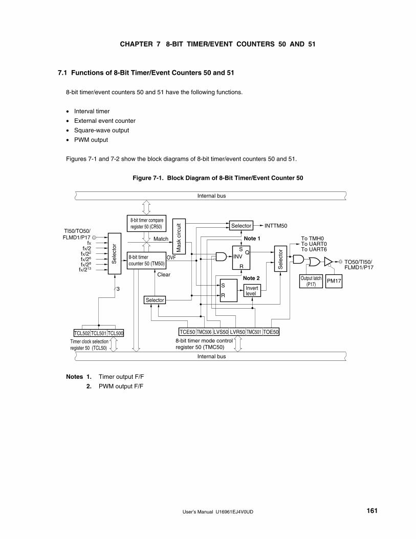
User’s Manual U16961EJ4V0UD 161
CHAPTER 7 8-BIT TIMER/EVENT COUNTERS 50 AND 51
7.1 Functions of 8-Bit Timer/Event Counters 50 and 51
8-bit timer/event counters 50 and 51 have the following functions.
• Interval timer
• External event counter
• Square-wave output
• PWM output
Figures 7-1 and 7-2 show the block diagrams of 8-bit timer/event counters 50 and 51.
Figure 7-1. Block Diagram of 8-Bit Timer/Event Counter 50
Internal bus
8-bit timer compareregister 50 (CR50)
TI50/TO50/FLMD1/P17
fX/22
fX/26
fX/28
fX/213
fXfX/2
Match
Mas
k ci
rcui
t
OVF
Clear
3
Selector
TCL502 TCL501 TCL500
Timer clock selectionregister 50 (TCL50)
Internal bus
TCE50 TMC506 LVS50 LVR50 TMC501 TOE50
Invertlevel
8-bit timer mode control register 50 (TMC50)
S
R
SQ
R
INV
Selector
To TMH0To UART0To UART6
INTTM50
TO50/TI50/FLMD1/P17
Note 1
Note 2S
elec
tor
8-bit timercounter 50 (TM50)S
elec
tor
Output latch(P17)
PM17
Notes 1. Timer output F/F
2. PWM output F/F
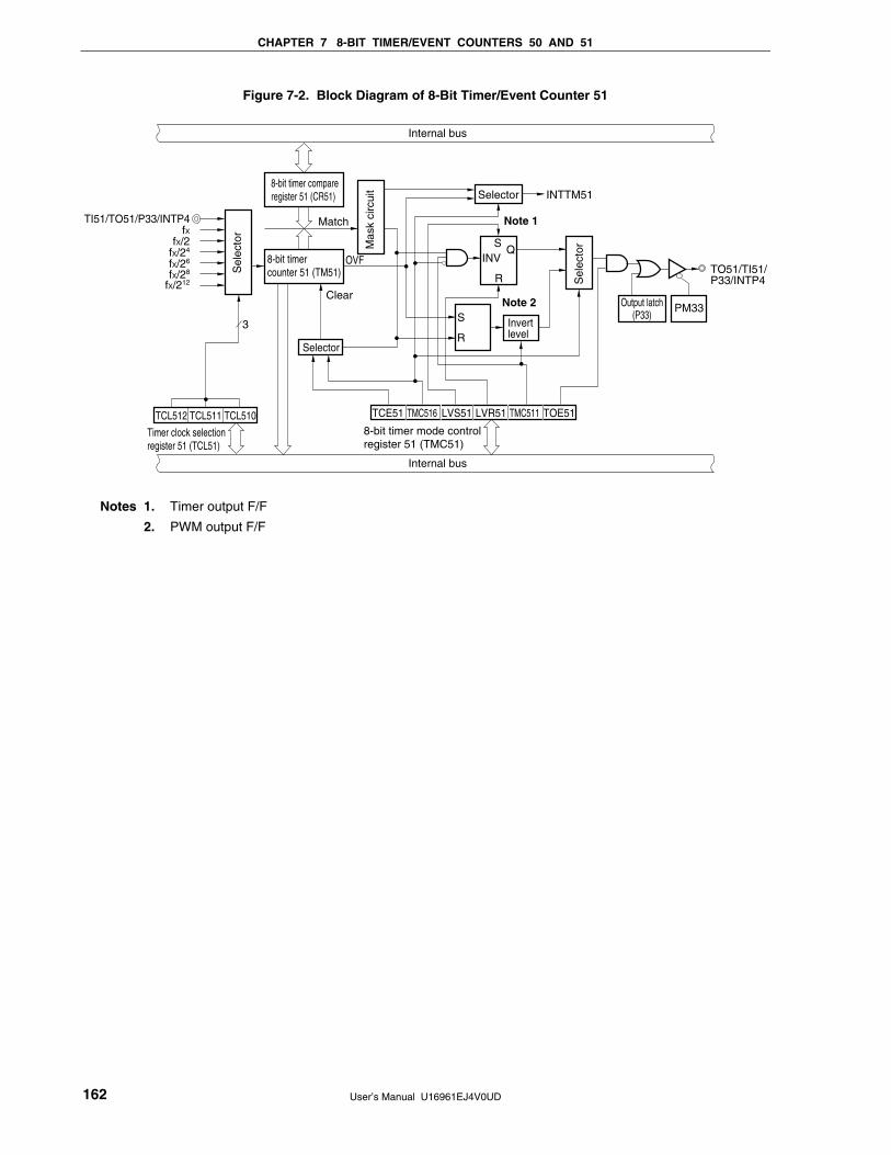
CHAPTER 7 8-BIT TIMER/EVENT COUNTERS 50 AND 51
User’s Manual U16961EJ4V0UD 162
Figure 7-2. Block Diagram of 8-Bit Timer/Event Counter 51
Internal bus
8-bit timer compareregister 51 (CR51)
TI51/TO51/P33/INTP4
fX/28
fX/212
fXfX/2
Match
Mas
k ci
rcui
t
OVF
Clear
3
Selector
TCL512 TCL511 TCL510
Timer clock selectionregister 51 (TCL51)
Internal bus
TCE51 TMC516 LVS51 LVR51 TMC511 TOE51
Invertlevel
8-bit timer mode control register 51 (TMC51)
S
R
SQ
R
INV
Selector INTTM51
TO51/TI51/P33/INTP4
Note 1
Note 2
Sel
ecto
r
8-bit timercounter 51 (TM51)S
elec
tor
Output latch(P33)
PM33
fX/26fX/24
Notes 1. Timer output F/F
2. PWM output F/F
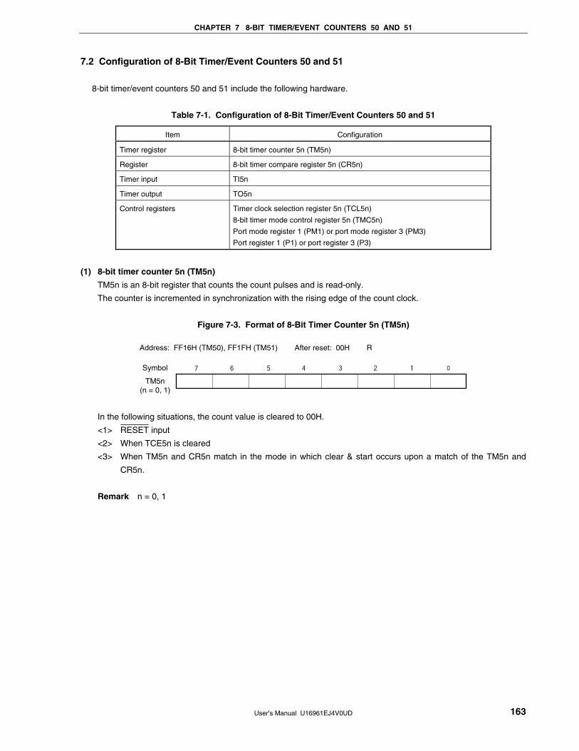
CHAPTER 7 8-BIT TIMER/EVENT COUNTERS 50 AND 51
User’s Manual U16961EJ4V0UD 163
7.2 Configuration of 8-Bit Timer/Event Counters 50 and 51
8-bit timer/event counters 50 and 51 include the following hardware.
Table 7-1. Configuration of 8-Bit Timer/Event Counters 50 and 51
Item Configuration
Timer register 8-bit timer counter 5n (TM5n)
Register 8-bit timer compare register 5n (CR5n)
Timer input TI5n
Timer output TO5n
Control registers Timer clock selection register 5n (TCL5n)
8-bit timer mode control register 5n (TMC5n)
Port mode register 1 (PM1) or port mode register 3 (PM3)
Port register 1 (P1) or port register 3 (P3)
(1) 8-bit timer counter 5n (TM5n)
TM5n is an 8-bit register that counts the count pulses and is read-only.
The counter is incremented in synchronization with the rising edge of the count clock.
Figure 7-3. Format of 8-Bit Timer Counter 5n (TM5n)
Symbol
TM5n(n = 0, 1)
Address: FF16H (TM50), FF1FH (TM51) After reset: 00H R
In the following situations, the count value is cleared to 00H.
<1> RESET input
<2> When TCE5n is cleared
<3> When TM5n and CR5n match in the mode in which clear & start occurs upon a match of the TM5n and
CR5n.
Remark n = 0, 1
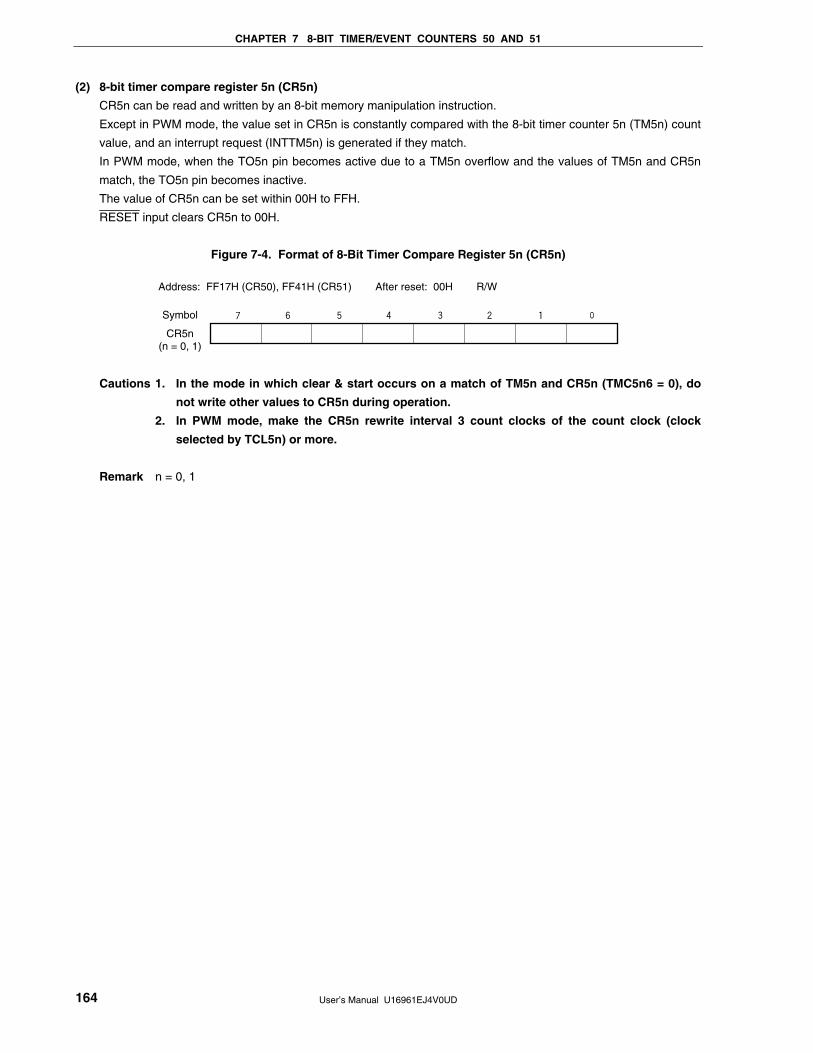
CHAPTER 7 8-BIT TIMER/EVENT COUNTERS 50 AND 51
User’s Manual U16961EJ4V0UD 164
(2) 8-bit timer compare register 5n (CR5n)
CR5n can be read and written by an 8-bit memory manipulation instruction.
Except in PWM mode, the value set in CR5n is constantly compared with the 8-bit timer counter 5n (TM5n) count
value, and an interrupt request (INTTM5n) is generated if they match.
In PWM mode, when the TO5n pin becomes active due to a TM5n overflow and the values of TM5n and CR5n
match, the TO5n pin becomes inactive.
The value of CR5n can be set within 00H to FFH.
RESET input clears CR5n to 00H.
Figure 7-4. Format of 8-Bit Timer Compare Register 5n (CR5n)
Symbol
CR5n(n = 0, 1)
Address: FF17H (CR50), FF41H (CR51) After reset: 00H R/W
Cautions 1. In the mode in which clear & start occurs on a match of TM5n and CR5n (TMC5n6 = 0), do
not write other values to CR5n during operation.
2. In PWM mode, make the CR5n rewrite interval 3 count clocks of the count clock (clock
selected by TCL5n) or more.
Remark n = 0, 1
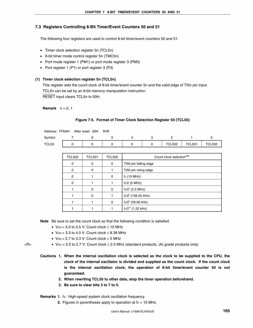
CHAPTER 7 8-BIT TIMER/EVENT COUNTERS 50 AND 51
User’s Manual U16961EJ4V0UD 165
7.3 Registers Controlling 8-Bit Timer/Event Counters 50 and 51
The following four registers are used to control 8-bit timer/event counters 50 and 51.
• Timer clock selection register 5n (TCL5n)
• 8-bit timer mode control register 5n (TMC5n)
• Port mode register 1 (PM1) or port mode register 3 (PM3)
• Port register 1 (P1) or port register 3 (P3)
(1) Timer clock selection register 5n (TCL5n)
This register sets the count clock of 8-bit timer/event counter 5n and the valid edge of TI5n pin input.
TCL5n can be set by an 8-bit memory manipulation instruction.
RESET input clears TCL5n to 00H.
Remark n = 0, 1
Figure 7-5. Format of Timer Clock Selection Register 50 (TCL50)
Address: FF6AH After reset: 00H R/W
Symbol 7 6 5 4 3 2 1 0
TCL50 0 0 0 0 0 TCL502 TCL501 TCL500
TCL502 TCL501 TCL500 Count clock selectionNote
0 0 0 TI50 pin falling edge
0 0 1 TI50 pin rising edge
0 1 0 fX (10 MHz)
0 1 1 fX/2 (5 MHz)
1 0 0 fX/22 (2.5 MHz)
1 0 1 fX/26 (156.25 kHz)
1 1 0 fX/28 (39.06 kHz)
1 1 1 fX/213 (1.22 kHz)
Note Be sure to set the count clock so that the following condition is satisfied.
• VDD = 4.0 to 5.5 V: Count clock ≤ 10 MHz
• VDD = 3.3 to 4.0 V: Count clock ≤ 8.38 MHz
• VDD = 2.7 to 3.3 V: Count clock ≤ 5 MHz
• VDD = 2.5 to 2.7 V: Count clock ≤ 2.5 MHz (standard products, (A) grade products only)
Cautions 1. When the internal oscillation clock is selected as the clock to be supplied to the CPU, the
clock of the internal oscillator is divided and supplied as the count clock. If the count clock
is the internal oscillation clock, the operation of 8-bit timer/event counter 50 is not
guaranteed.
2. When rewriting TCL50 to other data, stop the timer operation beforehand.
3. Be sure to clear bits 3 to 7 to 0.
Remarks 1. fX: High-speed system clock oscillation frequency
2. Figures in parentheses apply to operation at fX = 10 MHz.
<R>
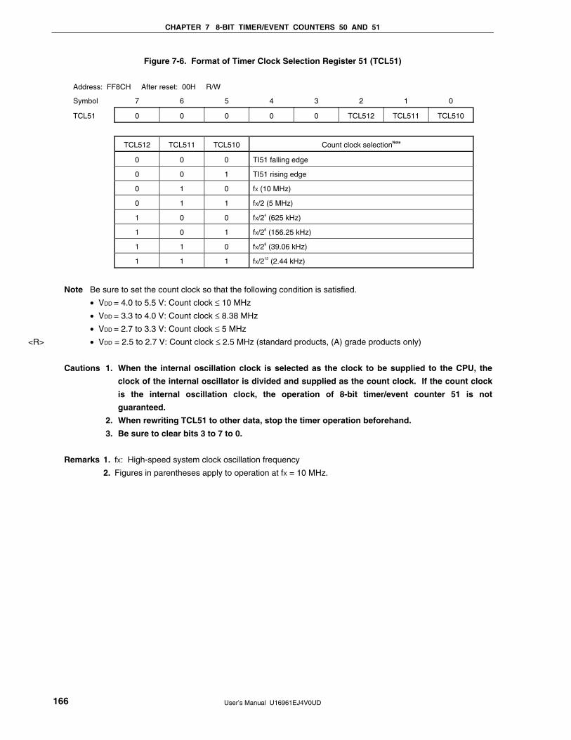
CHAPTER 7 8-BIT TIMER/EVENT COUNTERS 50 AND 51
User’s Manual U16961EJ4V0UD 166
Figure 7-6. Format of Timer Clock Selection Register 51 (TCL51)
Address: FF8CH After reset: 00H R/W
Symbol 7 6 5 4 3 2 1 0
TCL51 0 0 0 0 0 TCL512 TCL511 TCL510
TCL512 TCL511 TCL510 Count clock selectionNote
0 0 0 TI51 falling edge
0 0 1 TI51 rising edge
0 1 0 fX (10 MHz)
0 1 1 fX/2 (5 MHz)
1 0 0 fX/24 (625 kHz)
1 0 1 fX/26 (156.25 kHz)
1 1 0 fX/28 (39.06 kHz)
1 1 1 fX/212 (2.44 kHz)
Note Be sure to set the count clock so that the following condition is satisfied.
• VDD = 4.0 to 5.5 V: Count clock ≤ 10 MHz
• VDD = 3.3 to 4.0 V: Count clock ≤ 8.38 MHz
• VDD = 2.7 to 3.3 V: Count clock ≤ 5 MHz
• VDD = 2.5 to 2.7 V: Count clock ≤ 2.5 MHz (standard products, (A) grade products only)
Cautions 1. When the internal oscillation clock is selected as the clock to be supplied to the CPU, the
clock of the internal oscillator is divided and supplied as the count clock. If the count clock
is the internal oscillation clock, the operation of 8-bit timer/event counter 51 is not
guaranteed.
2. When rewriting TCL51 to other data, stop the timer operation beforehand.
3. Be sure to clear bits 3 to 7 to 0.
Remarks 1. fX: High-speed system clock oscillation frequency
2. Figures in parentheses apply to operation at fX = 10 MHz.
<R>
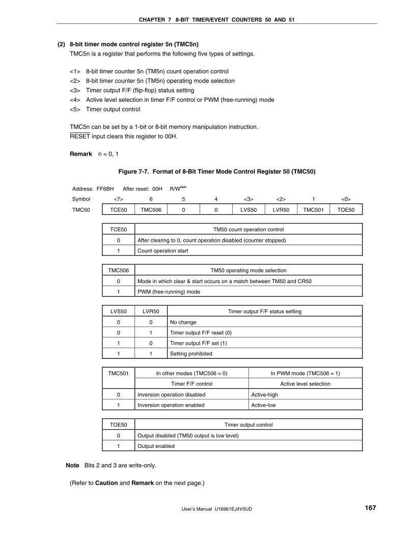
CHAPTER 7 8-BIT TIMER/EVENT COUNTERS 50 AND 51
User’s Manual U16961EJ4V0UD 167
(2) 8-bit timer mode control register 5n (TMC5n)
TMC5n is a register that performs the following five types of settings.
<1> 8-bit timer counter 5n (TM5n) count operation control
<2> 8-bit timer counter 5n (TM5n) operating mode selection
<3> Timer output F/F (flip-flop) status setting
<4> Active level selection in timer F/F control or PWM (free-running) mode
<5> Timer output control
TMC5n can be set by a 1-bit or 8-bit memory manipulation instruction.
RESET input clears this register to 00H.
Remark n = 0, 1
Figure 7-7. Format of 8-Bit Timer Mode Control Register 50 (TMC50)
Address: FF6BH After reset: 00H R/WNote
Symbol <7> 6 5 4 <3> <2> 1 <0>
TMC50 TCE50 TMC506 0 0 LVS50 LVR50 TMC501 TOE50
TCE50 TM50 count operation control
0 After clearing to 0, count operation disabled (counter stopped)
1 Count operation start
TMC506 TM50 operating mode selection
0 Mode in which clear & start occurs on a match between TM50 and CR50
1 PWM (free-running) mode
LVS50 LVR50 Timer output F/F status setting
0 0 No change
0 1 Timer output F/F reset (0)
1 0 Timer output F/F set (1)
1 1 Setting prohibited
In other modes (TMC506 = 0) In PWM mode (TMC506 = 1) TMC501
Timer F/F control Active level selection
0 Inversion operation disabled Active-high
1 Inversion operation enabled Active-low
TOE50 Timer output control
0 Output disabled (TM50 output is low level)
1 Output enabled
Note Bits 2 and 3 are write-only.
(Refer to Caution and Remark on the next page.)
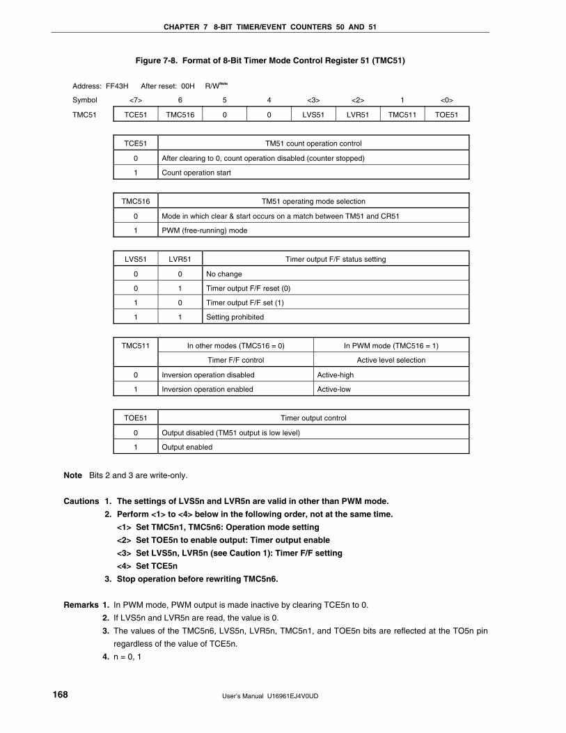
CHAPTER 7 8-BIT TIMER/EVENT COUNTERS 50 AND 51
User’s Manual U16961EJ4V0UD 168
Figure 7-8. Format of 8-Bit Timer Mode Control Register 51 (TMC51)
Address: FF43H After reset: 00H R/WNote
Symbol <7> 6 5 4 <3> <2> 1 <0>
TMC51 TCE51 TMC516 0 0 LVS51 LVR51 TMC511 TOE51
TCE51 TM51 count operation control
0 After clearing to 0, count operation disabled (counter stopped)
1 Count operation start
TMC516 TM51 operating mode selection
0 Mode in which clear & start occurs on a match between TM51 and CR51
1 PWM (free-running) mode
LVS51 LVR51 Timer output F/F status setting
0 0 No change
0 1 Timer output F/F reset (0)
1 0 Timer output F/F set (1)
1 1 Setting prohibited
In other modes (TMC516 = 0) In PWM mode (TMC516 = 1) TMC511
Timer F/F control Active level selection
0 Inversion operation disabled Active-high
1 Inversion operation enabled Active-low
TOE51 Timer output control
0 Output disabled (TM51 output is low level)
1 Output enabled
Note Bits 2 and 3 are write-only.
Cautions 1. The settings of LVS5n and LVR5n are valid in other than PWM mode.
2. Perform <1> to <4> below in the following order, not at the same time.
<1> Set TMC5n1, TMC5n6: Operation mode setting
<2> Set TOE5n to enable output: Timer output enable
<3> Set LVS5n, LVR5n (see Caution 1): Timer F/F setting
<4> Set TCE5n
3. Stop operation before rewriting TMC5n6.
Remarks 1. In PWM mode, PWM output is made inactive by clearing TCE5n to 0.
2. If LVS5n and LVR5n are read, the value is 0.
3. The values of the TMC5n6, LVS5n, LVR5n, TMC5n1, and TOE5n bits are reflected at the TO5n pin
regardless of the value of TCE5n.
4. n = 0, 1
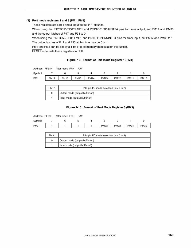
CHAPTER 7 8-BIT TIMER/EVENT COUNTERS 50 AND 51
User’s Manual U16961EJ4V0UD 169
(3) Port mode registers 1 and 3 (PM1, PM3)
These registers set port 1 and 3 input/output in 1-bit units.
When using the P17/TO50/TI50/FLMD1 and P33/TO51/TI51/INTP4 pins for timer output, set PM17 and PM33
and the output latches of P17 and P33 to 0.
When using the P17/TO50/TI50/FLMD1 and P33/TO51/TI51/INTP4 pins for timer input, set PM17 and PM33 to 1.
The output latches of P17 and P33 at this time may be 0 or 1.
PM1 and PM3 can be set by a 1-bit or 8-bit memory manipulation instruction.
RESET input sets these registers to FFH.
Figure 7-9. Format of Port Mode Register 1 (PM1)
Address: FF21H After reset: FFH R/W
Symbol 7 6 5 4 3 2 1 0
PM1 PM17 PM16 PM15 PM14 PM13 PM12 PM11 PM10
PM1n P1n pin I/O mode selection (n = 0 to 7)
0 Output mode (output buffer on)
1 Input mode (output buffer off)
Figure 7-10. Format of Port Mode Register 3 (PM3)
Address: FF23H After reset: FFH R/W
Symbol 7 6 5 4 3 2 1 0
PM3 1 1 1 1 PM33 PM32 PM31 PM30
PM3n P3n pin I/O mode selection (n = 0 to 3)
0 Output mode (output buffer on)
1 Input mode (output buffer off)
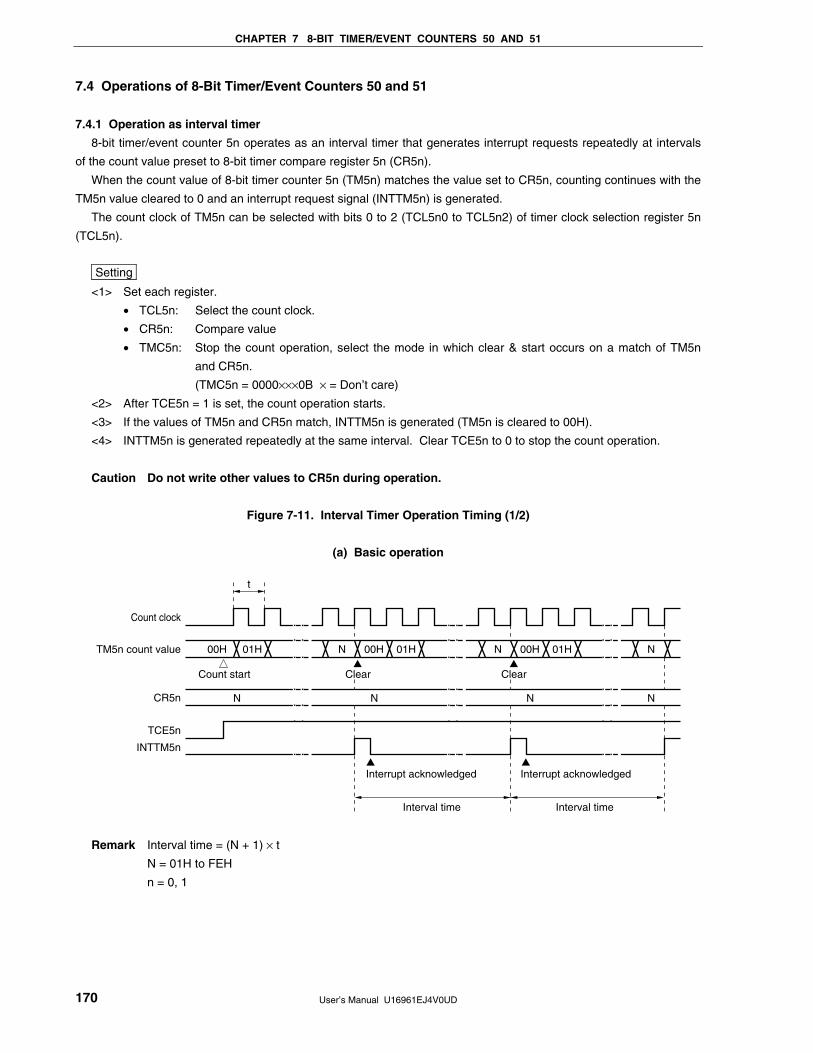
CHAPTER 7 8-BIT TIMER/EVENT COUNTERS 50 AND 51
User’s Manual U16961EJ4V0UD 170
7.4 Operations of 8-Bit Timer/Event Counters 50 and 51
7.4.1 Operation as interval timer
8-bit timer/event counter 5n operates as an interval timer that generates interrupt requests repeatedly at intervals
of the count value preset to 8-bit timer compare register 5n (CR5n).
When the count value of 8-bit timer counter 5n (TM5n) matches the value set to CR5n, counting continues with the
TM5n value cleared to 0 and an interrupt request signal (INTTM5n) is generated.
The count clock of TM5n can be selected with bits 0 to 2 (TCL5n0 to TCL5n2) of timer clock selection register 5n
(TCL5n).
Setting
<1> Set each register.
• TCL5n: Select the count clock.
• CR5n: Compare value
• TMC5n: Stop the count operation, select the mode in which clear & start occurs on a match of TM5n
and CR5n.
(TMC5n = 0000×××0B × = Don’t care)
<2> After TCE5n = 1 is set, the count operation starts.
<3> If the values of TM5n and CR5n match, INTTM5n is generated (TM5n is cleared to 00H).
<4> INTTM5n is generated repeatedly at the same interval. Clear TCE5n to 0 to stop the count operation.
Caution Do not write other values to CR5n during operation.
Figure 7-11. Interval Timer Operation Timing (1/2)
(a) Basic operation
t
Count clock
TM5n count value
CR5n
TCE5n
INTTM5n
Count start Clear Clear
00H 01H N 00H 01H N 00H 01H N
NNNN
Interrupt acknowledged Interrupt acknowledged
Interval timeInterval time
Remark Interval time = (N + 1) × t
N = 01H to FEH
n = 0, 1
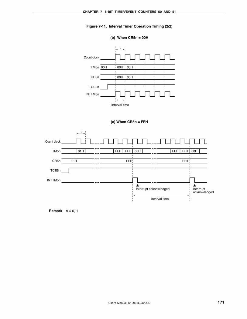
CHAPTER 7 8-BIT TIMER/EVENT COUNTERS 50 AND 51
User’s Manual U16961EJ4V0UD 171
Figure 7-11. Interval Timer Operation Timing (2/2)
(b) When CR5n = 00H
t
Interval time
Count clock
TM5n
CR5n
TCE5n
INTTM5n
00H 00H 00H
00H 00H
(c) When CR5n = FFH
t
Count clock
TM5n
CR5n
TCE5n
INTTM5n
01H FEH FFH 00H FEH FFH 00H
FFHFFHFFH
Interval time
Interrupt acknowledged
Interrupt acknowledged
Remark n = 0, 1
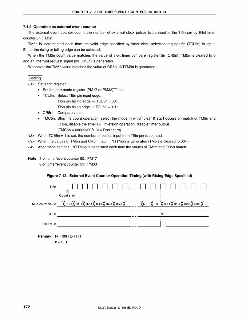
CHAPTER 7 8-BIT TIMER/EVENT COUNTERS 50 AND 51
User’s Manual U16961EJ4V0UD 172
7.4.2 Operation as external event counter
The external event counter counts the number of external clock pulses to be input to the TI5n pin by 8-bit timer
counter 5n (TM5n).
TM5n is incremented each time the valid edge specified by timer clock selection register 5n (TCL5n) is input.
Either the rising or falling edge can be selected.
When the TM5n count value matches the value of 8-bit timer compare register 5n (CR5n), TM5n is cleared to 0
and an interrupt request signal (INTTM5n) is generated.
Whenever the TM5n value matches the value of CR5n, INTTM5n is generated.
Setting
<1> Set each register.
• Set the port mode register (PM17 or PM33)Note to 1.
• TCL5n: Select TI5n pin input edge.
TI5n pin falling edge → TCL5n = 00H
TI5n pin rising edge → TCL5n = 01H
• CR5n: Compare value
• TMC5n: Stop the count operation, select the mode in which clear & start occurs on match of TM5n and
CR5n, disable the timer F/F inversion operation, disable timer output.
(TMC5n = 0000××00B × = Don’t care)
<2> When TCE5n = 1 is set, the number of pulses input from TI5n pin is counted.
<3> When the values of TM5n and CR5n match, INTTM5n is generated (TM5n is cleared to 00H).
<4> After these settings, INTTM5n is generated each time the values of TM5n and CR5n match.
Note 8-bit timer/event counter 50: PM17
8-bit timer/event counter 51: PM33
Figure 7-12. External Event Counter Operation Timing (with Rising Edge Specified)
TI5n
TM5n count value
CR5n
INTTM5n
00H 01H 02H 03H 04H 05H N – 1 N 00H 01H 02H 03H
N
Count start
Remark N = 00H to FFH
n = 0, 1
CHAPTER 7 8-BIT TIMER/EVENT COUNTERS 50 AND 51
User’s Manual U16961EJ4V0UD 173
7.4.3 Square-wave output operation
A square wave with any selected frequency is output at intervals determined by the value preset to 8-bit timer
compare register 5n (CR5n).
The TO5n pin output status is inverted at intervals determined by the count value preset to CR5n by setting bit 0
(TOE5n) of 8-bit timer mode control register 5n (TMC5n) to 1. This enables a square wave with any selected
frequency to be output (duty = 50%).
Setting
<1> Set each register.
• Clear the port output latch (P17 or P33)Note and port mode register (PM17 or PM33)Note to 0.
• TCL5n: Select the count clock.
• CR5n: Compare value
• TMC5n: Stop the count operation, select the mode in which clear & start occurs on a match of TM5n and
CR5n.
LVS5n LVR5n Timer Output F/F Status Setting
1 0 High-level output
0 1 Low-level output
Timer output F/F inversion enabled
Timer output enabled
(TMC5n = 00001011B or 00000111B)
<2> After TCE5n = 1 is set, the count operation starts.
<3> The timer output F/F is inverted by a match of TM5n and CR5n. After INTTM5n is generated, TM5n is
cleared to 00H.
<4> After these settings, the timer output F/F is inverted at the same interval and a square wave is output from
TO5n.
The frequency is as follows.
Frequency = 1/2t (N + 1)
(N: 00H to FFH)
Note 8-bit timer/event counter 50: P17, PM17
8-bit timer/event counter 51: P33, PM33
Caution Do not write other values to CR5n during operation.
Remark n = 0, 1
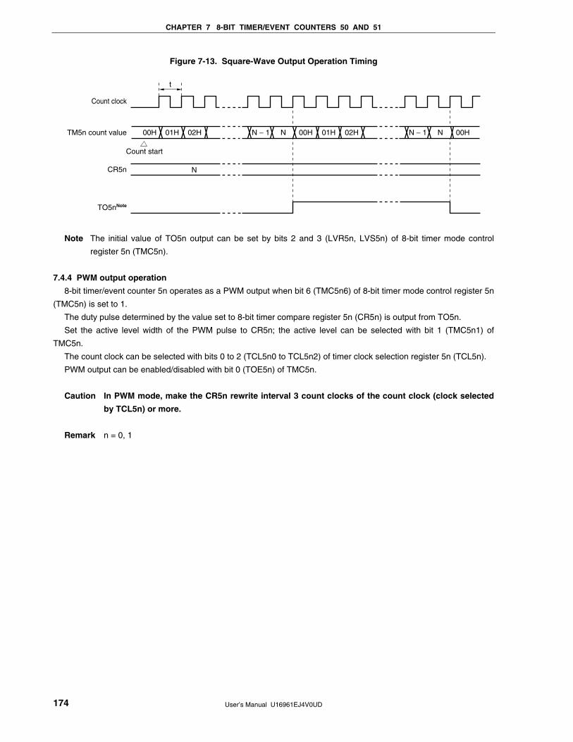
CHAPTER 7 8-BIT TIMER/EVENT COUNTERS 50 AND 51
User’s Manual U16961EJ4V0UD 174
Figure 7-13. Square-Wave Output Operation Timing
Count clock
TM5n count value 00H 01H 02H N − 1 N
N
00H N − 1 N 00H01H 02H
CR5n
TO5nNote
t
Count start
Note The initial value of TO5n output can be set by bits 2 and 3 (LVR5n, LVS5n) of 8-bit timer mode control
register 5n (TMC5n).
7.4.4 PWM output operation
8-bit timer/event counter 5n operates as a PWM output when bit 6 (TMC5n6) of 8-bit timer mode control register 5n
(TMC5n) is set to 1.
The duty pulse determined by the value set to 8-bit timer compare register 5n (CR5n) is output from TO5n.
Set the active level width of the PWM pulse to CR5n; the active level can be selected with bit 1 (TMC5n1) of
TMC5n.
The count clock can be selected with bits 0 to 2 (TCL5n0 to TCL5n2) of timer clock selection register 5n (TCL5n).
PWM output can be enabled/disabled with bit 0 (TOE5n) of TMC5n.
Caution In PWM mode, make the CR5n rewrite interval 3 count clocks of the count clock (clock selected
by TCL5n) or more.
Remark n = 0, 1
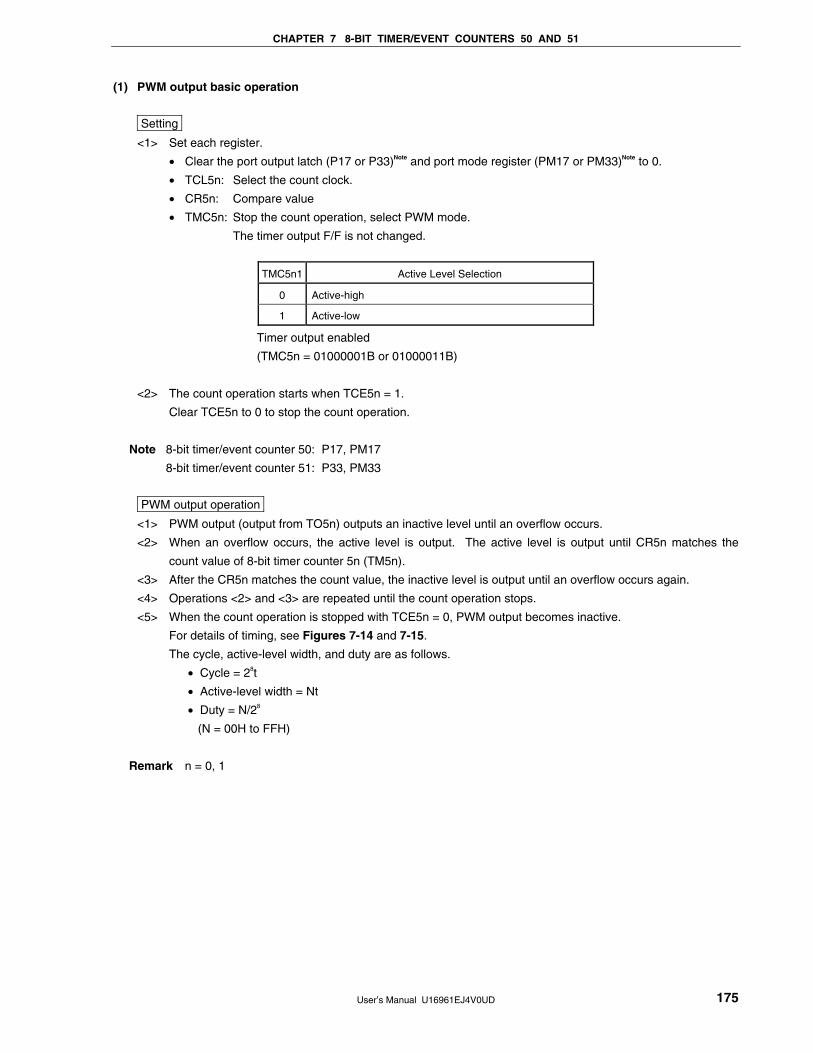
CHAPTER 7 8-BIT TIMER/EVENT COUNTERS 50 AND 51
User’s Manual U16961EJ4V0UD 175
(1) PWM output basic operation
Setting
<1> Set each register.
• Clear the port output latch (P17 or P33)Note and port mode register (PM17 or PM33)Note to 0.
• TCL5n: Select the count clock.
• CR5n: Compare value
• TMC5n: Stop the count operation, select PWM mode.
The timer output F/F is not changed.
TMC5n1 Active Level Selection
0 Active-high
1 Active-low
Timer output enabled
(TMC5n = 01000001B or 01000011B)
<2> The count operation starts when TCE5n = 1.
Clear TCE5n to 0 to stop the count operation.
Note 8-bit timer/event counter 50: P17, PM17
8-bit timer/event counter 51: P33, PM33
PWM output operation
<1> PWM output (output from TO5n) outputs an inactive level until an overflow occurs.
<2> When an overflow occurs, the active level is output. The active level is output until CR5n matches the
count value of 8-bit timer counter 5n (TM5n).
<3> After the CR5n matches the count value, the inactive level is output until an overflow occurs again.
<4> Operations <2> and <3> are repeated until the count operation stops.
<5> When the count operation is stopped with TCE5n = 0, PWM output becomes inactive.
For details of timing, see Figures 7-14 and 7-15.
The cycle, active-level width, and duty are as follows.
• Cycle = 28t
• Active-level width = Nt
• Duty = N/28
(N = 00H to FFH)
Remark n = 0, 1
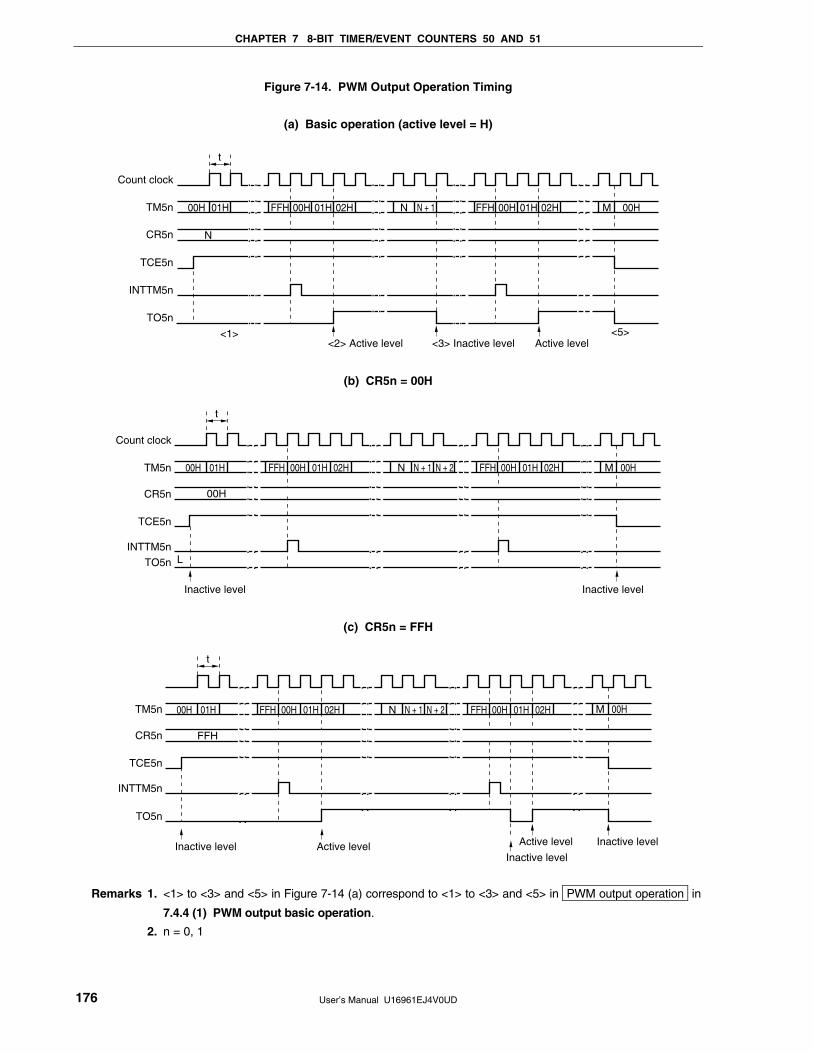
CHAPTER 7 8-BIT TIMER/EVENT COUNTERS 50 AND 51
User’s Manual U16961EJ4V0UD 176
Figure 7-14. PWM Output Operation Timing
(a) Basic operation (active level = H)
Count clock
TM5n
CR5n
TCE5n
INTTM5n
TO5n
00H 01H FFH 00H 01H 02H N N + 1 FFH 00H 01H 02H M 00H
N
<2> Active level<1>
<3> Inactive level Active level<5>
t
(b) CR5n = 00H
Count clock
TM5n
CR5n
TCE5n
INTTM5n
TO5n
Inactive level Inactive level
01H00H FFH 00H 01H 02H N N + 1 FFH 00H 01H 02H M 00H
00H
N + 2
L
t
(c) CR5n = FFH
TM5n
CR5n
TCE5n
INTTM5n
TO5n
01H00H FFH 00H 01H 02H N N + 1 FFH 00H 01H 02H M 00H
FFH
N + 2
Inactive level Active levelInactive level
Active level Inactive level
t
Remarks 1. <1> to <3> and <5> in Figure 7-14 (a) correspond to <1> to <3> and <5> in PWM output operation in
7.4.4 (1) PWM output basic operation.
2. n = 0, 1
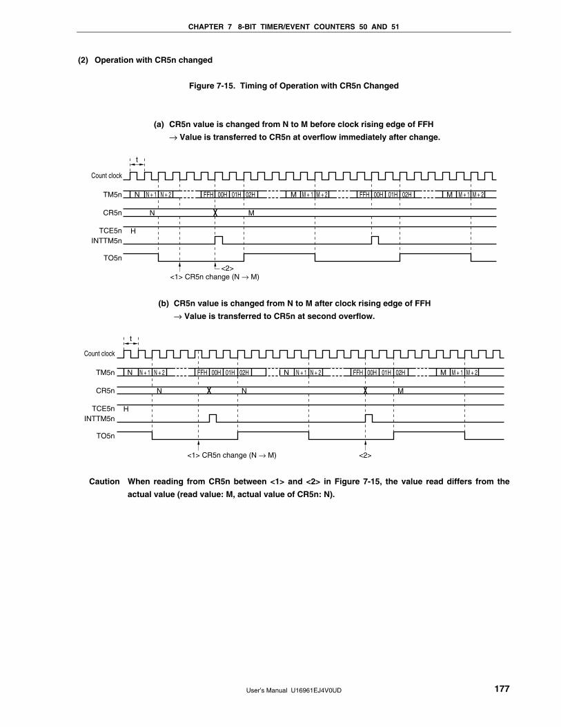
CHAPTER 7 8-BIT TIMER/EVENT COUNTERS 50 AND 51
User’s Manual U16961EJ4V0UD 177
(2) Operation with CR5n changed
Figure 7-15. Timing of Operation with CR5n Changed
(a) CR5n value is changed from N to M before clock rising edge of FFH
→ Value is transferred to CR5n at overflow immediately after change.
Count clock
TM5n
CR5n
TCE5nINTTM5n
TO5n
<1> CR5n change (N → M)
N N + 1 N + 2 FFH 00H 01H M M + 1 M + 2 FFH 00H 01H 02H M M + 1 M + 2
N
02H
M
H
<2>
t
(b) CR5n value is changed from N to M after clock rising edge of FFH
→ Value is transferred to CR5n at second overflow.
Count clock
TM5n
CR5n
TCE5nINTTM5n
TO5n
N N + 1 N + 2 FFH 00H 01H N N + 1 N + 2 FFH 00H 01H 02H
N
02H
N
H
M
M M + 1 M + 2
<1> CR5n change (N → M) <2>
t
Caution When reading from CR5n between <1> and <2> in Figure 7-15, the value read differs from the
actual value (read value: M, actual value of CR5n: N).
CHAPTER 7 8-BIT TIMER/EVENT COUNTERS 50 AND 51
User’s Manual U16961EJ4V0UD 178
7.5 Cautions for 8-Bit Timer/Event Counters 50 and 51
(1) Timer start error
An error of up to one clock may occur in the time required for a match signal to be generated after timer start.
This is because 8-bit timer counters 50 and 51 (TM50, TM51) are started asynchronously to the count clock.
Figure 7-16. 8-Bit Timer Counter 5n Start Timing
Count clock
TM5n count value 00H 01H 02H 03H 04H
Timer start
Remark n = 0, 1
User’s Manual U16961EJ4V0UD 179
CHAPTER 8 8-BIT TIMERS H0 AND H1
8.1 Functions of 8-Bit Timers H0 and H1
8-bit timers H0 and H1 have the following functions.
• Interval timer
• PWM output mode
• Square-wave output
• Carrier generator mode (8-bit timer H1 only)
8.2 Configuration of 8-Bit Timers H0 and H1
8-bit timers H0 and H1 include the following hardware.
Table 8-1. Configuration of 8-Bit Timers H0 and H1
Item Configuration
Timer register 8-bit timer counter Hn
Registers 8-bit timer H compare register 0n (CMP0n)
8-bit timer H compare register 1n (CMP1n)
Timer output TOHn
Control registers 8-bit timer H mode register n (TMHMDn)
8-bit timer H carrier control register 1 (TMCYC1)Note
Port mode register 1 (PM1)
Port register 1 (P1)
Note 8-bit timer H1 only
Remark n = 0, 1
Figures 8-1 and 8-2 show the block diagrams.
CH
AP
TE
R 8 8-B
IT T
IME
RS
H0 A
ND
H1
User’s M
anual U16961E
J4V0U
D
180
Figure 8-1. Block Diagram of 8-Bit Timer H0
TMHE0 CKS02 CKS01 CKS00 TMMD01 TMMD00 TOLEV0 TOEN0
TOH0/P15
INTTMH0
fXfX/2
fX/22
fX/26
fX/210
10
F/F
R
3 2
PM15Match
Internal bus
8-bit timer H mode register 0 (TMHMD0)
8-bit timer H compare register
10 (CMP10)
Decoder
Selector
Interrupt generator
Output controller
Levelinversion
PWM mode signal
Timer H enable signal
Clear
8-bit timer H compare register
00 (CMP00)
Output latch(P15)
8-bit timer/event counter 50 output
Sel
ecto
r
8-bit timercounter H0
CH
AP
TE
R 8 8-B
IT T
IME
RS
H0 A
ND
H1
User’s M
anual U16961E
J4V0U
D
181
Figure 8-2. Block Diagram of 8-Bit Timer H1
Match
Internal bus
TMHE1 CKS12 CKS11 CKS10 TMMD11 TMMD10 TOLEV1 TOEN1 8-bit timer Hcompare
register 11(CMP11)
Decoder
TOH1/INTP5/P16
8-bit timer H carrier control register 1(TMCYC1)
INTTMH1
INTTM51
Selector
fXfX/22
fX/24
fX/26
fX/212
fR/27
Interruptgenerator
Outputcontroller
Levelinversion
PM16Output latch(P16)
10
F/F
R
PWM mode signal
Carrier generator mode signal
Timer H enable signal
3 2
8-bit timer Hcompare
register 01(CMP01)
8-bit timercounter H1
Clear
RMC1 NRZB1 NRZ1
Reload/interrupt control
8-bit timer H mode register 1 (TMHMD1)
Sel
ecto
r
CHAPTER 8 8-BIT TIMERS H0 AND H1
User’s Manual U16961EJ4V0UD 182
(1) 8-bit timer H compare register 0n (CMP0n)
This register can be read/written by an 8-bit memory manipulation instruction.
RESET input clears this register to 00H.
Figure 8-3. Format of 8-Bit Timer H Compare Register 0n (CMP0n)
Symbol
CMP0n(n = 0, 1)
Address: FF18H (CMP00), FF1AH (CMP01) After reset: 00H R/W
7 6 5 4 3 2 1 0
Caution CMP0n cannot be rewritten during timer count operation.
(2) 8-bit timer H compare register 1n (CMP1n)
This register can be read/written by an 8-bit memory manipulation instruction.
RESET input clears this register to 00H.
Figure 8-4. Format of 8-Bit Timer H Compare Register 1n (CMP1n)
Symbol
CMP1n(n = 0, 1)
Address: FF19H (CMP10), FF1BH (CMP11) After reset: 00H R/W
7 6 5 4 3 2 1 0
CMP1n can be rewritten during timer count operation.
An interrupt request signal (INTTMHn) is generated if the timer count values and CMP1n match after setting
CMP1n in carrier generator mode. The timer count value is cleared at the same time. If the CMP1n value is rewritten
during timer operation, transferring is performed at the timing at which the count value and CMP1n value match. If the
transfer timing and writing from CPU to CMP1n conflict, transfer is not performed.
Caution In the PWM output mode and carrier generator mode, be sure to set CMP1n when starting the
timer count operation (TMHEn = 1) after the timer count operation was stopped (TMHEn = 0) (be
sure to set again even if setting the same value to CMP1n).
Remark n = 0, 1
CHAPTER 8 8-BIT TIMERS H0 AND H1
User’s Manual U16961EJ4V0UD 183
8.3 Registers Controlling 8-Bit Timers H0 and H1
The following four registers are used to control 8-bit timers H0 and H1.
• 8-bit timer H mode register n (TMHMDn)
• 8-bit timer H carrier control register 1 (TMCYC1)Note
• Port mode register 1 (PM1)
• Port register 1 (P1)
Note 8-bit timer H1 only
(1) 8-bit timer H mode register n (TMHMDn)
This register controls the mode of timer H.
This register can be set by a 1-bit or 8-bit memory manipulation instruction.
RESET input clears this register to 00H.
Remark n = 0, 1
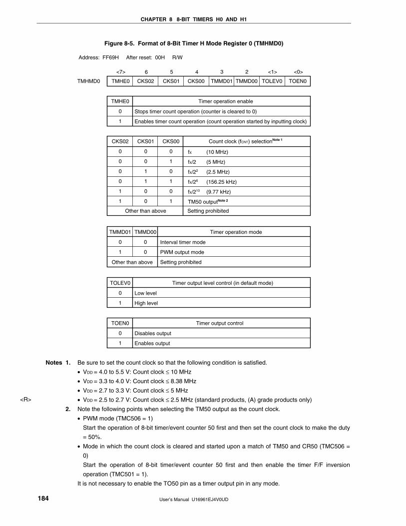
CHAPTER 8 8-BIT TIMERS H0 AND H1
User’s Manual U16961EJ4V0UD 184
Figure 8-5. Format of 8-Bit Timer H Mode Register 0 (TMHMD0)
TMHE0
Stops timer count operation (counter is cleared to 0)
Enables timer count operation (count operation started by inputting clock)
TMHE0
0
1
Timer operation enable
TMHMD0 CKS02 CKS01 CKS00 TMMD01 TMMD00 TOLEV0 TOEN0
Address: FF69H After reset: 00H R/W
fX
fX/2
fX/22
fX/26
fX/210
TM50 outputNote 2
CKS02
0
0
0
0
1
1
CKS01
0
0
1
1
0
0
CKS00
0
1
0
1
0
1
(10 MHz)
(5 MHz)
(2.5 MHz)
(156.25 kHz)
(9.77 kHz)
Count clock (fCNT) selectionNote 1
Setting prohibitedOther than above
Interval timer mode
PWM output mode
Setting prohibited
TMMD01
0
1
TMMD00
0
0
Timer operation mode
Low level
High level
TOLEV0
0
1
Timer output level control (in default mode)
Disables output
Enables output
TOEN0
0
1
Timer output control
Other than above
<7> 6 5 4 3 2 <1> <0>
Notes 1. Be sure to set the count clock so that the following condition is satisfied.
• VDD = 4.0 to 5.5 V: Count clock ≤ 10 MHz
• VDD = 3.3 to 4.0 V: Count clock ≤ 8.38 MHz
• VDD = 2.7 to 3.3 V: Count clock ≤ 5 MHz
• VDD = 2.5 to 2.7 V: Count clock ≤ 2.5 MHz (standard products, (A) grade products only)
2. Note the following points when selecting the TM50 output as the count clock.
• PWM mode (TMC506 = 1)
Start the operation of 8-bit timer/event counter 50 first and then set the count clock to make the duty
= 50%.
• Mode in which the count clock is cleared and started upon a match of TM50 and CR50 (TMC506 =
0)
Start the operation of 8-bit timer/event counter 50 first and then enable the timer F/F inversion
operation (TMC501 = 1).
It is not necessary to enable the TO50 pin as a timer output pin in any mode.
<R>
CHAPTER 8 8-BIT TIMERS H0 AND H1
User’s Manual U16961EJ4V0UD 185
Cautions 1. When the internal oscillation clock is selected as the clock to be supplied to the CPU, the
clock of the internal oscillator is divided and supplied as the count clock. If the count clock
is the internal oscillation clock, the operation of 8-bit timer H0 is not guaranteed.
2. When TMHE0 = 1, setting the other bits of TMHMD0 is prohibited.
3. In the PWM output mode, be sure to set 8-bit timer H compare register 10 (CMP10) when
starting the timer count operation (TMHE0 = 1) after the timer count operation was stopped
(TMHE0 = 0) (be sure to set again even if setting the same value to CMP10).
Remarks 1. fX: High-speed system clock oscillation frequency
2. Figures in parentheses apply to operation at fX = 10 MHz.
3. TMC506: Bit 6 of 8-bit timer mode control register 50 (TMC50)
TMC501: Bit 1 of TMC50
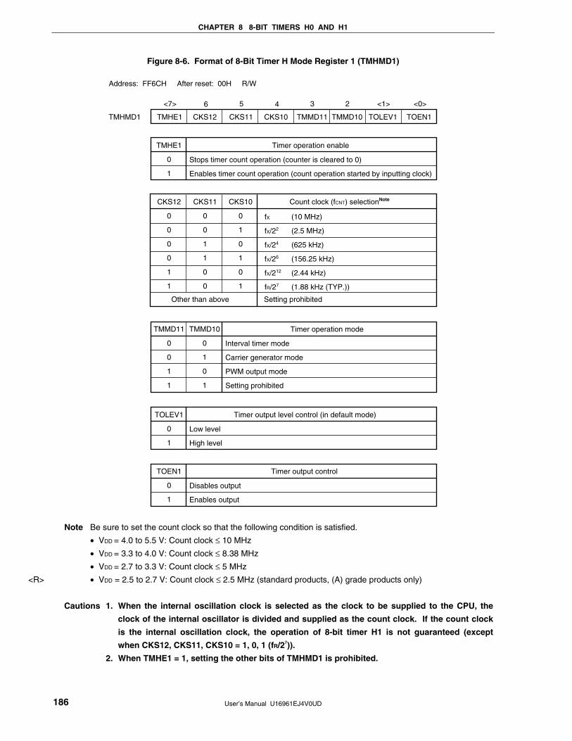
CHAPTER 8 8-BIT TIMERS H0 AND H1
User’s Manual U16961EJ4V0UD 186
Figure 8-6. Format of 8-Bit Timer H Mode Register 1 (TMHMD1)
TMHE1
Stops timer count operation (counter is cleared to 0)
Enables timer count operation (count operation started by inputting clock)
TMHE1
0
1
Timer operation enable
TMHMD1 CKS12 CKS11 CKS10 TMMD11 TMMD10 TOLEV1 TOEN1
Address: FF6CH After reset: 00H R/W
fX
fX/22
fX/24
fX/26
fX/212
fR/27
CKS12
0
0
0
0
1
1
CKS11
0
0
1
1
0
0
CKS10
0
1
0
1
0
1
(10 MHz)
(2.5 MHz)
(625 kHz)
(156.25 kHz)
(2.44 kHz)
(1.88 kHz (TYP.))
Count clock (fCNT) selectionNote
Setting prohibitedOther than above
Interval timer mode
Carrier generator mode
PWM output mode
Setting prohibited
TMMD11
0
0
1
1
TMMD10
0
1
0
1
Timer operation mode
Low level
High level
TOLEV1
0
1
Timer output level control (in default mode)
Disables output
Enables output
TOEN1
0
1
Timer output control
<7> 6 5 4 3 2 <1> <0>
Note Be sure to set the count clock so that the following condition is satisfied.
• VDD = 4.0 to 5.5 V: Count clock ≤ 10 MHz
• VDD = 3.3 to 4.0 V: Count clock ≤ 8.38 MHz
• VDD = 2.7 to 3.3 V: Count clock ≤ 5 MHz
• VDD = 2.5 to 2.7 V: Count clock ≤ 2.5 MHz (standard products, (A) grade products only)
Cautions 1. When the internal oscillation clock is selected as the clock to be supplied to the CPU, the
clock of the internal oscillator is divided and supplied as the count clock. If the count clock
is the internal oscillation clock, the operation of 8-bit timer H1 is not guaranteed (except
when CKS12, CKS11, CKS10 = 1, 0, 1 (fR/27)).
2. When TMHE1 = 1, setting the other bits of TMHMD1 is prohibited.
<R>
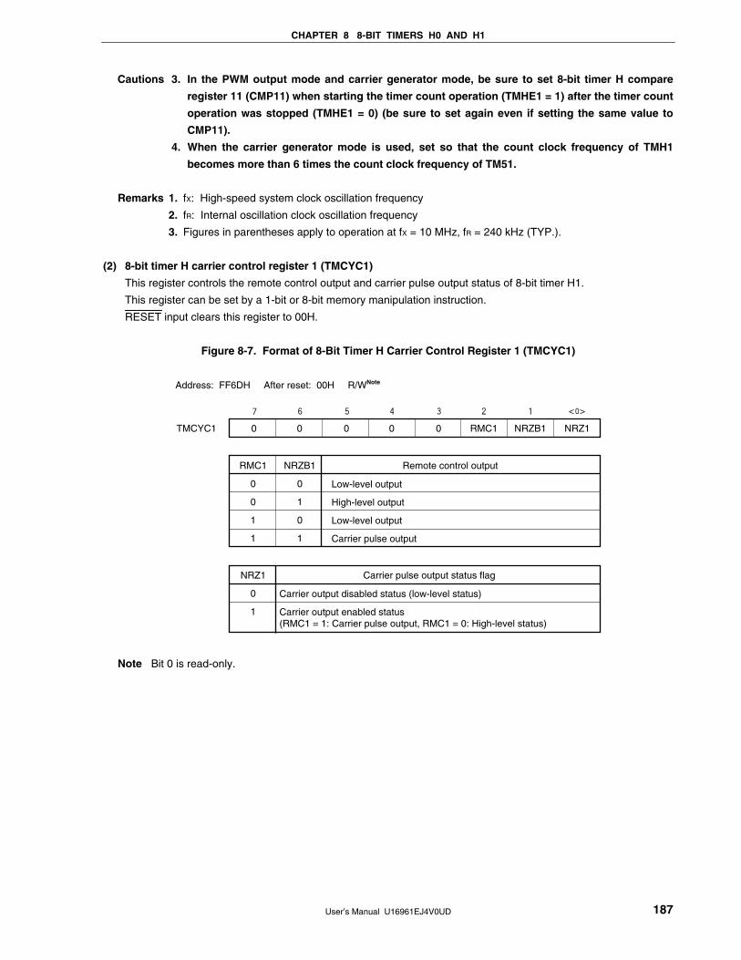
CHAPTER 8 8-BIT TIMERS H0 AND H1
User’s Manual U16961EJ4V0UD 187
Cautions 3. In the PWM output mode and carrier generator mode, be sure to set 8-bit timer H compare
register 11 (CMP11) when starting the timer count operation (TMHE1 = 1) after the timer count
operation was stopped (TMHE1 = 0) (be sure to set again even if setting the same value to
CMP11).
4. When the carrier generator mode is used, set so that the count clock frequency of TMH1
becomes more than 6 times the count clock frequency of TM51.
Remarks 1. fX: High-speed system clock oscillation frequency
2. fR: Internal oscillation clock oscillation frequency
3. Figures in parentheses apply to operation at fX = 10 MHz, fR = 240 kHz (TYP.).
(2) 8-bit timer H carrier control register 1 (TMCYC1)
This register controls the remote control output and carrier pulse output status of 8-bit timer H1.
This register can be set by a 1-bit or 8-bit memory manipulation instruction.
RESET input clears this register to 00H.
Figure 8-7. Format of 8-Bit Timer H Carrier Control Register 1 (TMCYC1)
0TMCYC1 0 0 0 0 RMC1 NRZB1 NRZ1
Address: FF6DH After reset: 00H R/WNote
Low-level output
High-level output
Low-level output
Carrier pulse output
RMC1
0
0
1
1
NRZB1
0
1
0
1
Remote control output
Carrier output disabled status (low-level status)
Carrier output enabled status (RMC1 = 1: Carrier pulse output, RMC1 = 0: High-level status)
NRZ1
0
1
Carrier pulse output status flag
< >
Note Bit 0 is read-only.
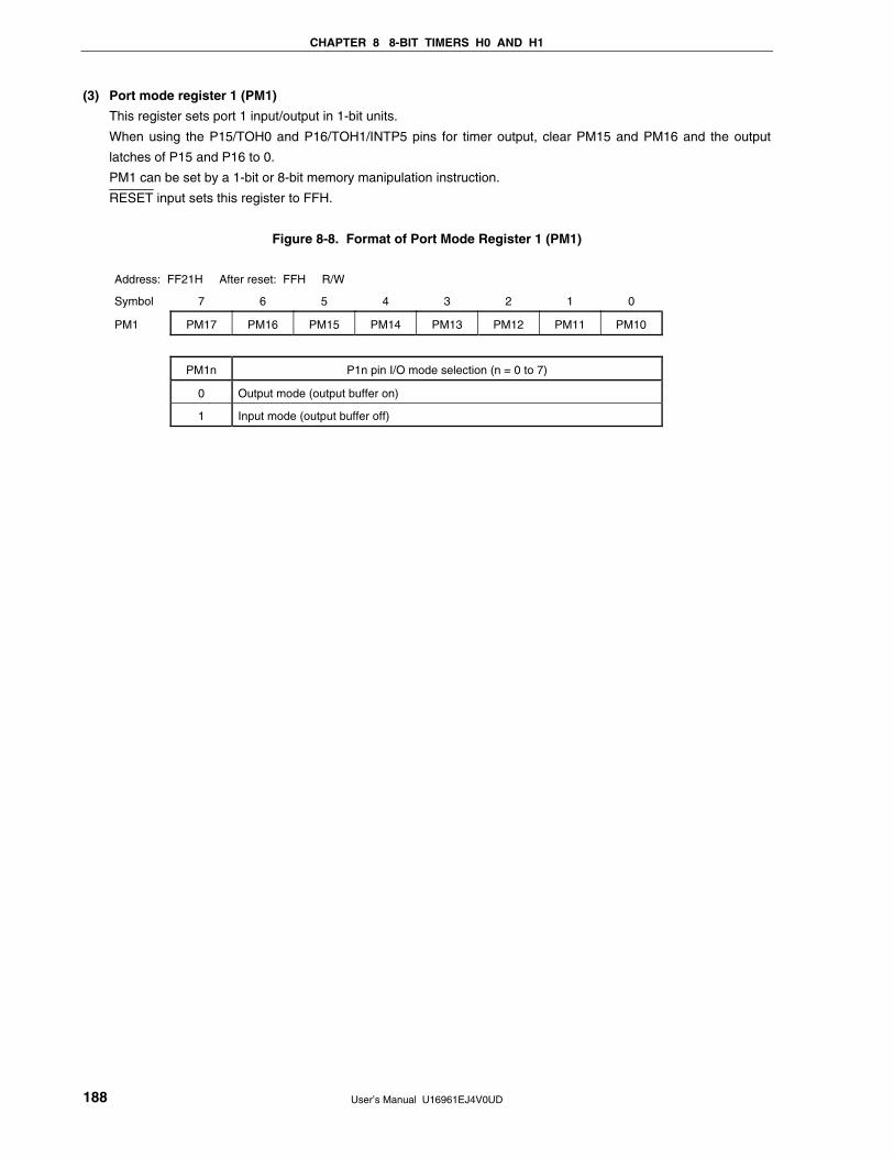
CHAPTER 8 8-BIT TIMERS H0 AND H1
User’s Manual U16961EJ4V0UD 188
(3) Port mode register 1 (PM1)
This register sets port 1 input/output in 1-bit units.
When using the P15/TOH0 and P16/TOH1/INTP5 pins for timer output, clear PM15 and PM16 and the output
latches of P15 and P16 to 0.
PM1 can be set by a 1-bit or 8-bit memory manipulation instruction.
RESET input sets this register to FFH.
Figure 8-8. Format of Port Mode Register 1 (PM1)
Address: FF21H After reset: FFH R/W
Symbol 7 6 5 4 3 2 1 0
PM1 PM17 PM16 PM15 PM14 PM13 PM12 PM11 PM10
PM1n P1n pin I/O mode selection (n = 0 to 7)
0 Output mode (output buffer on)
1 Input mode (output buffer off)
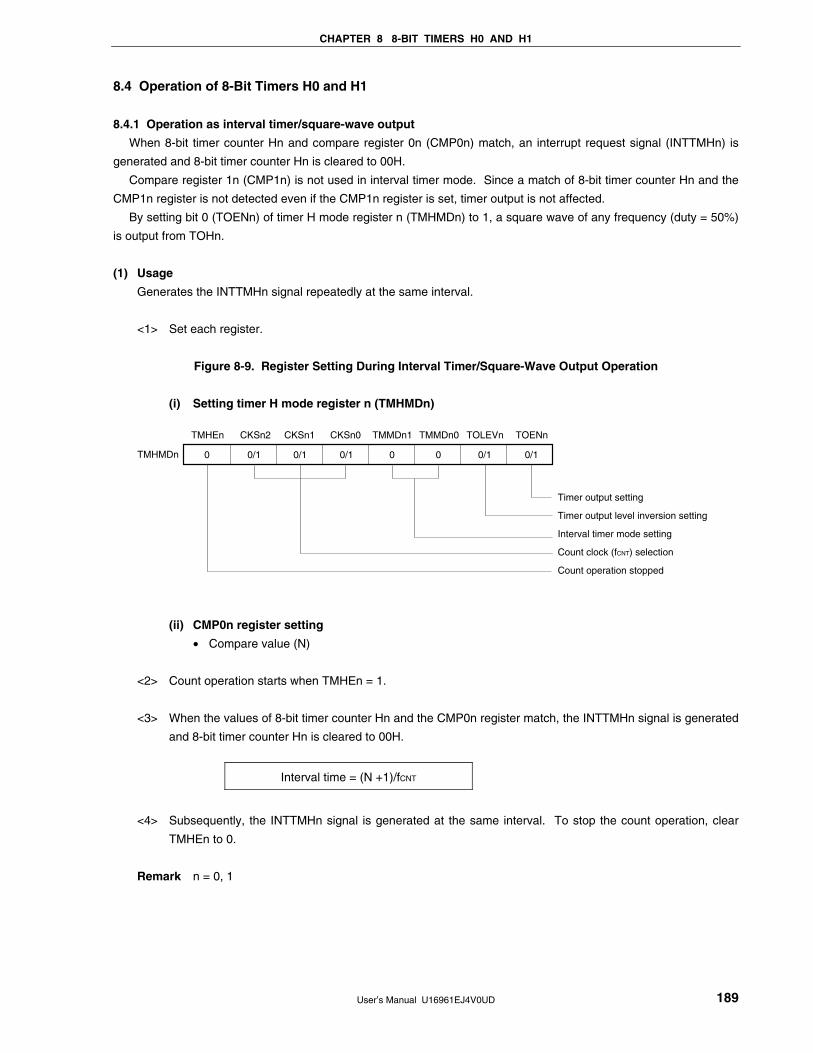
CHAPTER 8 8-BIT TIMERS H0 AND H1
User’s Manual U16961EJ4V0UD 189
8.4 Operation of 8-Bit Timers H0 and H1
8.4.1 Operation as interval timer/square-wave output
When 8-bit timer counter Hn and compare register 0n (CMP0n) match, an interrupt request signal (INTTMHn) is
generated and 8-bit timer counter Hn is cleared to 00H.
Compare register 1n (CMP1n) is not used in interval timer mode. Since a match of 8-bit timer counter Hn and the
CMP1n register is not detected even if the CMP1n register is set, timer output is not affected.
By setting bit 0 (TOENn) of timer H mode register n (TMHMDn) to 1, a square wave of any frequency (duty = 50%)
is output from TOHn.
(1) Usage
Generates the INTTMHn signal repeatedly at the same interval.
<1> Set each register.
Figure 8-9. Register Setting During Interval Timer/Square-Wave Output Operation
(i) Setting timer H mode register n (TMHMDn)
0 0/1 0/1 0/1 0 0 0/1 0/1
TMMDn0 TOLEVn TOENnCKSn1CKSn2TMHEn
TMHMDn
CKSn0 TMMDn1
Timer output setting
Timer output level inversion setting
Interval timer mode setting
Count clock (fCNT) selection
Count operation stopped
(ii) CMP0n register setting
• Compare value (N)
<2> Count operation starts when TMHEn = 1.
<3> When the values of 8-bit timer counter Hn and the CMP0n register match, the INTTMHn signal is generated
and 8-bit timer counter Hn is cleared to 00H.
Interval time = (N +1)/fCNT
<4> Subsequently, the INTTMHn signal is generated at the same interval. To stop the count operation, clear
TMHEn to 0.
Remark n = 0, 1
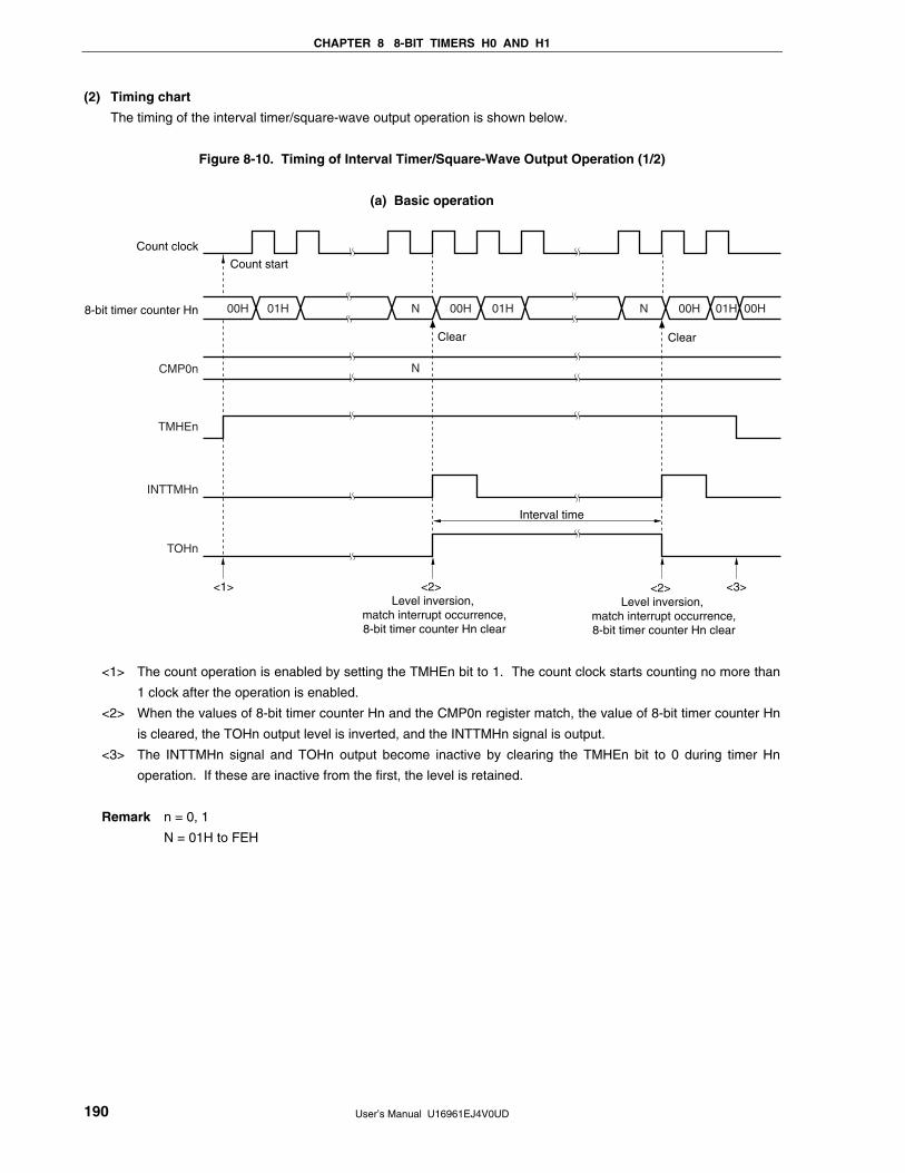
CHAPTER 8 8-BIT TIMERS H0 AND H1
User’s Manual U16961EJ4V0UD 190
(2) Timing chart
The timing of the interval timer/square-wave output operation is shown below.
Figure 8-10. Timing of Interval Timer/Square-Wave Output Operation (1/2)
(a) Basic operation
00H
Count clock
Count start
8-bit timer counter Hn
CMP0n
TMHEn
INTTMHn
TOHn
01H N
Clear
Interval time
Clear
N
00H 01H N 00H 01H 00H
<2> Level inversion,
match interrupt occurrence,8-bit timer counter Hn clear
<2> Level inversion,
match interrupt occurrence,8-bit timer counter Hn clear
<3><1>
<1> The count operation is enabled by setting the TMHEn bit to 1. The count clock starts counting no more than
1 clock after the operation is enabled.
<2> When the values of 8-bit timer counter Hn and the CMP0n register match, the value of 8-bit timer counter Hn
is cleared, the TOHn output level is inverted, and the INTTMHn signal is output.
<3> The INTTMHn signal and TOHn output become inactive by clearing the TMHEn bit to 0 during timer Hn
operation. If these are inactive from the first, the level is retained.
Remark n = 0, 1
N = 01H to FEH
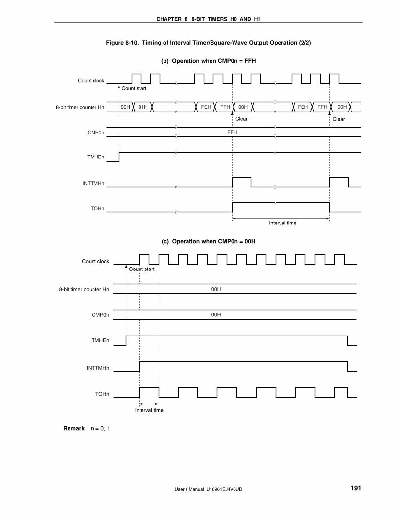
CHAPTER 8 8-BIT TIMERS H0 AND H1
User’s Manual U16961EJ4V0UD 191
Figure 8-10. Timing of Interval Timer/Square-Wave Output Operation (2/2)
(b) Operation when CMP0n = FFH
00H
Count clock
Count start
8-bit timer counter Hn
CMP0n
TMHEn
INTTMHn
TOHn
01H FEH
ClearClear
FFH 00H FEH FFH 00H
FFH
Interval time
(c) Operation when CMP0n = 00H
Count clock
Count start
8-bit timer counter Hn
CMP0n
TMHEn
INTTMHn
TOHn
00H
00H
Interval time
Remark n = 0, 1
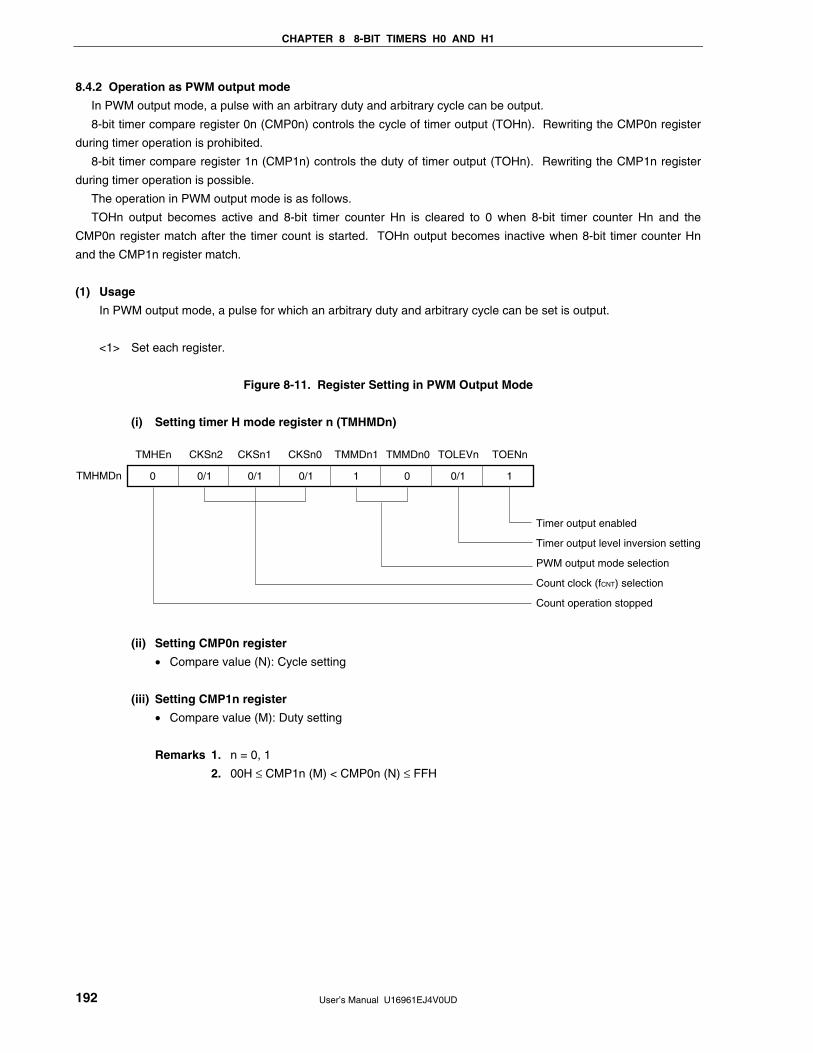
CHAPTER 8 8-BIT TIMERS H0 AND H1
User’s Manual U16961EJ4V0UD 192
8.4.2 Operation as PWM output mode
In PWM output mode, a pulse with an arbitrary duty and arbitrary cycle can be output.
8-bit timer compare register 0n (CMP0n) controls the cycle of timer output (TOHn). Rewriting the CMP0n register
during timer operation is prohibited.
8-bit timer compare register 1n (CMP1n) controls the duty of timer output (TOHn). Rewriting the CMP1n register
during timer operation is possible.
The operation in PWM output mode is as follows.
TOHn output becomes active and 8-bit timer counter Hn is cleared to 0 when 8-bit timer counter Hn and the
CMP0n register match after the timer count is started. TOHn output becomes inactive when 8-bit timer counter Hn
and the CMP1n register match.
(1) Usage
In PWM output mode, a pulse for which an arbitrary duty and arbitrary cycle can be set is output.
<1> Set each register.
Figure 8-11. Register Setting in PWM Output Mode
(i) Setting timer H mode register n (TMHMDn)
0 0/1 0/1 0/1 1 0 0/1 1
TMMDn0 TOLEVn TOENnCKSn1CKSn2TMHEn
TMHMDn
CKSn0 TMMDn1
Timer output enabled
Timer output level inversion setting
PWM output mode selection
Count clock (fCNT) selection
Count operation stopped
(ii) Setting CMP0n register
• Compare value (N): Cycle setting
(iii) Setting CMP1n register
• Compare value (M): Duty setting
Remarks 1. n = 0, 1
2. 00H ≤ CMP1n (M) < CMP0n (N) ≤ FFH
CHAPTER 8 8-BIT TIMERS H0 AND H1
User’s Manual U16961EJ4V0UD 193
<2> The count operation starts when TMHEn = 1.
<3> The CMP0n register is the compare register that is to be compared first after counter operation is enabled.
When the values of 8-bit timer counter Hn and the CMP0n register match, 8-bit timer counter Hn is cleared,
an interrupt request signal (INTTMHn) is generated, and TOHn output becomes active. At the same time,
the compare register to be compared with 8-bit timer counter Hn is changed from the CMP0n register to the
CMP1n register.
<4> When 8-bit timer counter Hn and the CMP1n register match, TOHn output becomes inactive and the
compare register to be compared with 8-bit timer counter Hn is changed from the CMP1n register to the
CMP0n register. At this time, 8-bit timer counter Hn is not cleared and the INTTMHn signal is not
generated.
<5> By performing procedures <3> and <4> repeatedly, a pulse with an arbitrary duty can be obtained.
<6> To stop the count operation, set TMHEn = 0.
If the setting value of the CMP0n register is N, the setting value of the CMP1n register is M, and the count clock
frequency is fCNT, the PWM pulse output cycle and duty are as follows.
PWM pulse output cycle = (N+1)/fCNT
Duty = Active width : Total width of PWM = (M + 1) : (N + 1)
Cautions 1. In PWM output mode, three operation clocks (signal selected using the CKSn2 to CKSn0
bits of the TMHMDn register) are required to transfer the CMP1n register value after
rewriting the register.
2. Be sure to set the CMP1n register when starting the timer count operation (TMHEn = 1) after
the timer count operation was stopped (TMHEn = 0) (be sure to set again even if setting the
same value to the CMP1n register).
Remark n = 0, 1
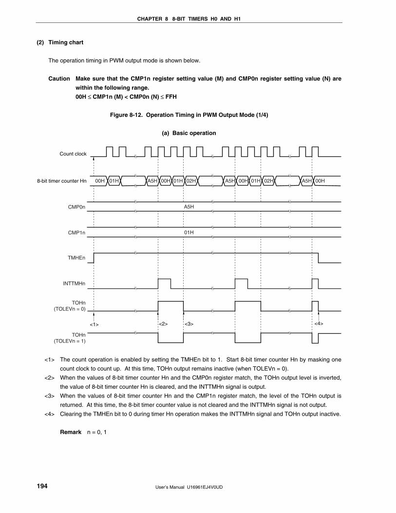
CHAPTER 8 8-BIT TIMERS H0 AND H1
User’s Manual U16961EJ4V0UD 194
(2) Timing chart
The operation timing in PWM output mode is shown below.
Caution Make sure that the CMP1n register setting value (M) and CMP0n register setting value (N) are
within the following range.
00H ≤ CMP1n (M) < CMP0n (N) ≤ FFH
Figure 8-12. Operation Timing in PWM Output Mode (1/4)
(a) Basic operation
Count clock
8-bit timer counter Hn
CMP0n
TMHEn
INTTMHn
TOHn(TOLEVn = 0)
TOHn(TOLEVn = 1)
00H 01H A5H 00H 01H 02H A5H 00H A5H 00H01H 02H
CMP1n
A5H
01H
<1> <2> <3> <4>
<1> The count operation is enabled by setting the TMHEn bit to 1. Start 8-bit timer counter Hn by masking one
count clock to count up. At this time, TOHn output remains inactive (when TOLEVn = 0).
<2> When the values of 8-bit timer counter Hn and the CMP0n register match, the TOHn output level is inverted,
the value of 8-bit timer counter Hn is cleared, and the INTTMHn signal is output.
<3> When the values of 8-bit timer counter Hn and the CMP1n register match, the level of the TOHn output is
returned. At this time, the 8-bit timer counter value is not cleared and the INTTMHn signal is not output.
<4> Clearing the TMHEn bit to 0 during timer Hn operation makes the INTTMHn signal and TOHn output inactive.
Remark n = 0, 1
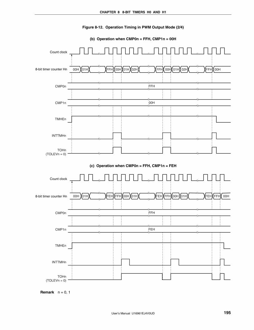
CHAPTER 8 8-BIT TIMERS H0 AND H1
User’s Manual U16961EJ4V0UD 195
Figure 8-12. Operation Timing in PWM Output Mode (2/4)
(b) Operation when CMP0n = FFH, CMP1n = 00H
Count clock
8-bit timer counter Hn
CMP0n
TMHEn
INTTMHn
TOHn(TOLEVn = 0)
00H 01H FFH 00H 01H 02H FFH 00H FFH 00H01H 02H
CMP1n
FFH
00H
(c) Operation when CMP0n = FFH, CMP1n = FEH
Count clock
8-bit timer counter Hn
CMP0n
TMHEn
INTTMHn
TOHn(TOLEVn = 0)
00H 01H FEH FFH 00H 01H FEH FFH 00H 01H FEH FFH 00H
CMP1n
FFH
FEH
Remark n = 0, 1
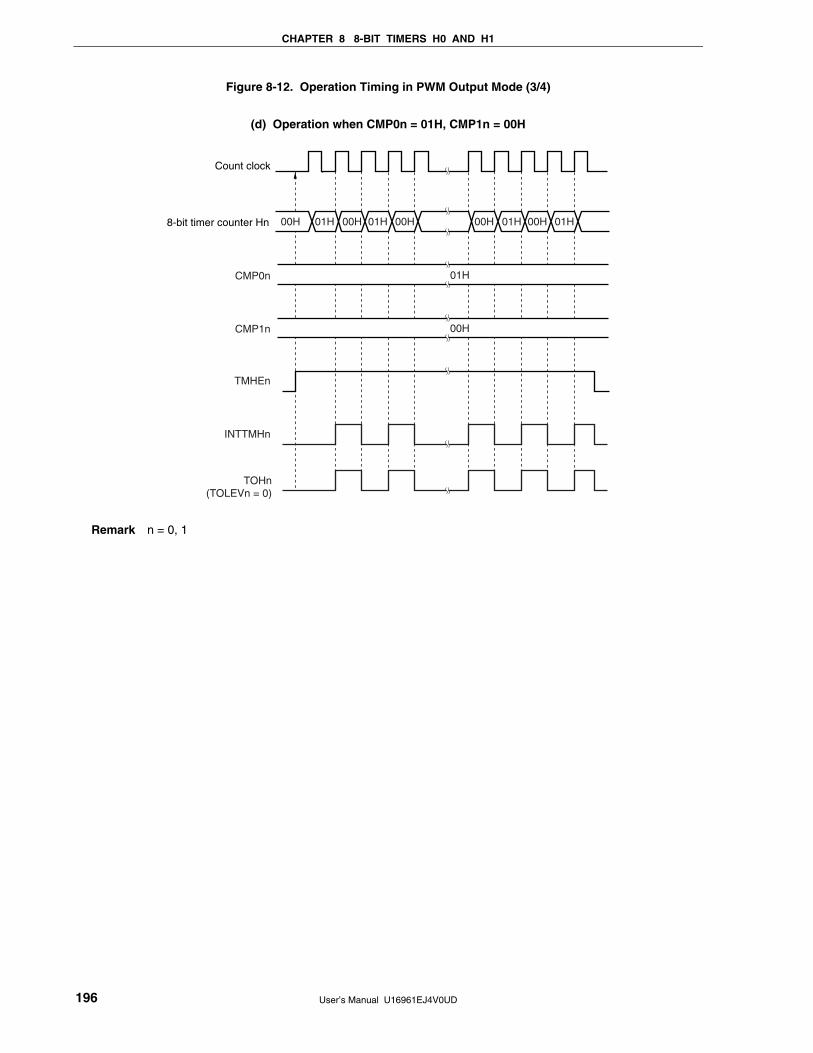
CHAPTER 8 8-BIT TIMERS H0 AND H1
User’s Manual U16961EJ4V0UD 196
Figure 8-12. Operation Timing in PWM Output Mode (3/4)
(d) Operation when CMP0n = 01H, CMP1n = 00H
Count clock
8-bit timer counter Hn
CMP0n
TMHEn
INTTMHn
TOHn(TOLEVn = 0)
01H
00H 01H 00H 01H 00H 00H 01H 00H 01H
CMP1n 00H
Remark n = 0, 1
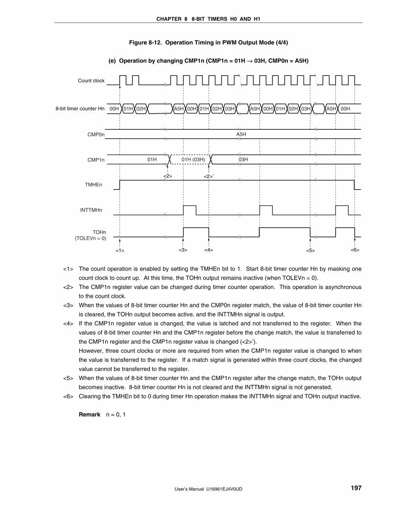
CHAPTER 8 8-BIT TIMERS H0 AND H1
User’s Manual U16961EJ4V0UD 197
Figure 8-12. Operation Timing in PWM Output Mode (4/4)
(e) Operation by changing CMP1n (CMP1n = 01H → 03H, CMP0n = A5H)
Count clock
8-bit timer counter Hn
CMP0n
TMHEn
INTTMHn
TOHn(TOLEVn = 0)
00H 01H 02H A5H 00H 01H 02H 03H A5H 00H 01H 02H 03H A5H 00H
CMP1n 01H
A5H
03H01H (03H)
<1> <3> <4>
<2> <2>'
<5> <6>
<1> The count operation is enabled by setting the TMHEn bit to 1. Start 8-bit timer counter Hn by masking one
count clock to count up. At this time, the TOHn output remains inactive (when TOLEVn = 0).
<2> The CMP1n register value can be changed during timer counter operation. This operation is asynchronous
to the count clock.
<3> When the values of 8-bit timer counter Hn and the CMP0n register match, the value of 8-bit timer counter Hn
is cleared, the TOHn output becomes active, and the INTTMHn signal is output.
<4> If the CMP1n register value is changed, the value is latched and not transferred to the register. When the
values of 8-bit timer counter Hn and the CMP1n register before the change match, the value is transferred to
the CMP1n register and the CMP1n register value is changed (<2>’).
However, three count clocks or more are required from when the CMP1n register value is changed to when
the value is transferred to the register. If a match signal is generated within three count clocks, the changed
value cannot be transferred to the register.
<5> When the values of 8-bit timer counter Hn and the CMP1n register after the change match, the TOHn output
becomes inactive. 8-bit timer counter Hn is not cleared and the INTTMHn signal is not generated.
<6> Clearing the TMHEn bit to 0 during timer Hn operation makes the INTTMHn signal and TOHn output inactive.
Remark n = 0, 1
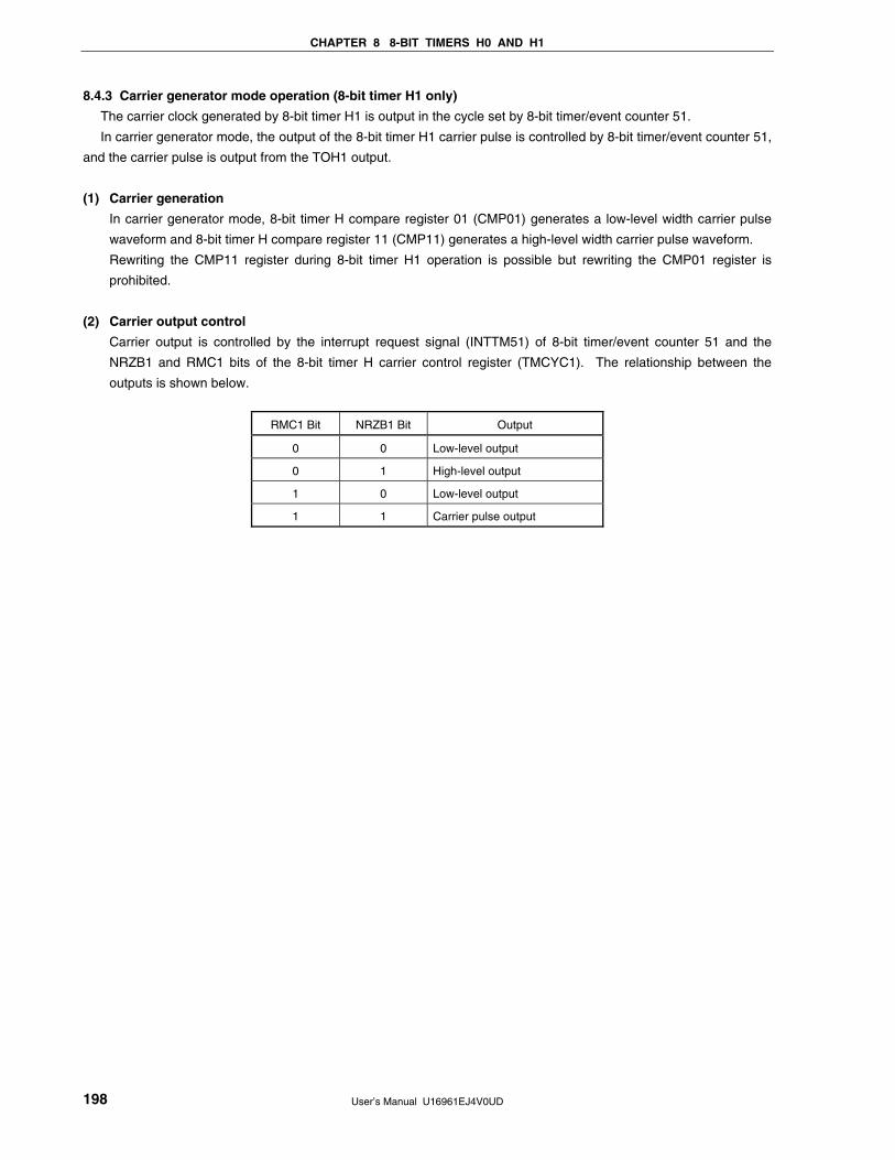
CHAPTER 8 8-BIT TIMERS H0 AND H1
User’s Manual U16961EJ4V0UD 198
8.4.3 Carrier generator mode operation (8-bit timer H1 only)
The carrier clock generated by 8-bit timer H1 is output in the cycle set by 8-bit timer/event counter 51.
In carrier generator mode, the output of the 8-bit timer H1 carrier pulse is controlled by 8-bit timer/event counter 51,
and the carrier pulse is output from the TOH1 output.
(1) Carrier generation
In carrier generator mode, 8-bit timer H compare register 01 (CMP01) generates a low-level width carrier pulse
waveform and 8-bit timer H compare register 11 (CMP11) generates a high-level width carrier pulse waveform.
Rewriting the CMP11 register during 8-bit timer H1 operation is possible but rewriting the CMP01 register is
prohibited.
(2) Carrier output control
Carrier output is controlled by the interrupt request signal (INTTM51) of 8-bit timer/event counter 51 and the
NRZB1 and RMC1 bits of the 8-bit timer H carrier control register (TMCYC1). The relationship between the
outputs is shown below.
RMC1 Bit NRZB1 Bit Output
0 0 Low-level output
0 1 High-level output
1 0 Low-level output
1 1 Carrier pulse output
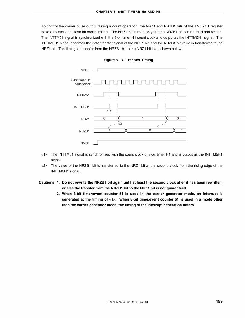
CHAPTER 8 8-BIT TIMERS H0 AND H1
User’s Manual U16961EJ4V0UD 199
To control the carrier pulse output during a count operation, the NRZ1 and NRZB1 bits of the TMCYC1 register
have a master and slave bit configuration. The NRZ1 bit is read-only but the NRZB1 bit can be read and written.
The INTTM51 signal is synchronized with the 8-bit timer H1 count clock and output as the INTTM5H1 signal. The
INTTM5H1 signal becomes the data transfer signal of the NRZ1 bit, and the NRZB1 bit value is transferred to the
NRZ1 bit. The timing for transfer from the NRZB1 bit to the NRZ1 bit is as shown below.
Figure 8-13. Transfer Timing
8-bit timer H1count clock
TMHE1
INTTM51
INTTM5H1
NRZ1
NRZB1
RMC1
1
1
10
0 0
<1>
<2>
<1> The INTTM51 signal is synchronized with the count clock of 8-bit timer H1 and is output as the INTTM5H1
signal.
<2> The value of the NRZB1 bit is transferred to the NRZ1 bit at the second clock from the rising edge of the
INTTM5H1 signal.
Cautions 1. Do not rewrite the NRZB1 bit again until at least the second clock after it has been rewritten,
or else the transfer from the NRZB1 bit to the NRZ1 bit is not guaranteed.
2. When 8-bit timer/event counter 51 is used in the carrier generator mode, an interrupt is
generated at the timing of <1>. When 8-bit timer/event counter 51 is used in a mode other
than the carrier generator mode, the timing of the interrupt generation differs.
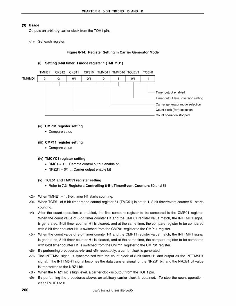
CHAPTER 8 8-BIT TIMERS H0 AND H1
User’s Manual U16961EJ4V0UD 200
(3) Usage
Outputs an arbitrary carrier clock from the TOH1 pin.
<1> Set each register.
Figure 8-14. Register Setting in Carrier Generator Mode
(i) Setting 8-bit timer H mode register 1 (TMHMD1)
0 0/1 0/1 0/1 0
Timer output enabled
Timer output level inversion setting
Carrier generator mode selection
Count clock (fCNT) selection
Count operation stopped
1 0/1 1
TMMD10 TOLEV1 TOEN1CKS11CKS12TMHE1
TMHMD1
CKS10 TMMD11
(ii) CMP01 register setting
• Compare value
(iii) CMP11 register setting
• Compare value
(iv) TMCYC1 register setting
• RMC1 = 1 ... Remote control output enable bit
• NRZB1 = 0/1 ... Carrier output enable bit
(v) TCL51 and TMC51 register setting
• Refer to 7.3 Registers Controlling 8-Bit Timer/Event Counters 50 and 51.
<2> When TMHE1 = 1, 8-bit timer H1 starts counting.
<3> When TCE51 of 8-bit timer mode control register 51 (TMC51) is set to 1, 8-bit timer/event counter 51 starts
counting.
<4> After the count operation is enabled, the first compare register to be compared is the CMP01 register.
When the count value of 8-bit timer counter H1 and the CMP01 register value match, the INTTMH1 signal
is generated, 8-bit timer counter H1 is cleared, and at the same time, the compare register to be compared
with 8-bit timer counter H1 is switched from the CMP01 register to the CMP11 register.
<5> When the count value of 8-bit timer counter H1 and the CMP11 register value match, the INTTMH1 signal
is generated, 8-bit timer counter H1 is cleared, and at the same time, the compare register to be compared
with 8-bit timer counter H1 is switched from the CMP11 register to the CMP01 register.
<6> By performing procedures <4> and <5> repeatedly, a carrier clock is generated.
<7> The INTTM51 signal is synchronized with the count clock of 8-bit timer H1 and output as the INTTM5H1
signal. The INTTM5H1 signal becomes the data transfer signal for the NRZB1 bit, and the NRZB1 bit value
is transferred to the NRZ1 bit.
<8> When the NRZ1 bit is high level, a carrier clock is output from the TOH1 pin.
<9> By performing the procedures above, an arbitrary carrier clock is obtained. To stop the count operation,
clear TMHE1 to 0.
CHAPTER 8 8-BIT TIMERS H0 AND H1
User’s Manual U16961EJ4V0UD 201
If the setting value of the CMP01 register is N, the setting value of the CMP11 register is M, and the count clock
frequency is fCNT, the carrier clock output cycle and duty are as follows.
Carrier clock output cycle = (N + M + 2)/fCNT
Duty = High-level width : Carrier clock output width = ( M + 1) : (N + M + 2)
Cautions 1. Be sure to set the CMP11 register when starting the timer count operation (TMHE1 = 1) after
the timer count operation was stopped (TMHE1 = 0) (be sure to set again even if setting the
same value to the CMP11 register).
2. Set so that the count clock frequency of TMH1 becomes more than 6 times the count clock
frequency of TM51.
(4) Timing chart
The carrier output control timing is shown below.
Cautions 1. Set the values of the CMP01 and CMP11 registers in a range of 01H to FFH.
2. In the carrier generator mode, three operating clocks (signal selected by CKS12 to CKS10
bits of TMHMD1 register) or more are required from when the CMP11 register value is
changed to when the value is transferred to the register.
3. Be sure to set the RMC1 bit before the count operation is started.
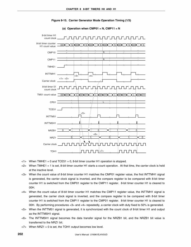
CHAPTER 8 8-BIT TIMERS H0 AND H1
User’s Manual U16961EJ4V0UD 202
Figure 8-15. Carrier Generator Mode Operation Timing (1/3)
(a) Operation when CMP01 = N, CMP11 = N
CMP10
CMP11
TMHE1
INTTMH1
Carrier clock
00H N 00H N 00H N 00H N 00H N 00H N
N
N
8-bit timer 51count clock
TM51 count value
CR51
TCE51
TOH1
0
0
1
1
0
0
1
1
0
0
INTTM51
NRZB1
NRZ1
Carrier clock
00H 01H L 00H 01H L 00H 01H L 00H 01H 00H 01HL
L
INTTM5H1
<1> <2><3> <4>
<5>
<6>
<7>
8-bit timer H1count clock
8-bit timer counterH1 count value
<1> When TMHE1 = 0 and TCE51 = 0, 8-bit timer counter H1 operation is stopped.
<2> When TMHE1 = 1 is set, 8-bit timer counter H1 starts a count operation. At that time, the carrier clock is held
at the inactive level.
<3> When the count value of 8-bit timer counter H1 matches the CMP01 register value, the first INTTMH1 signal
is generated, the carrier clock signal is inverted, and the compare register to be compared with 8-bit timer
counter H1 is switched from the CMP01 register to the CMP11 register. 8-bit timer counter H1 is cleared to
00H.
<4> When the count value of 8-bit timer counter H1 matches the CMP11 register value, the INTTMH1 signal is
generated, the carrier clock signal is inverted, and the compare register to be compared with 8-bit timer
counter H1 is switched from the CMP11 register to the CMP01 register. 8-bit timer counter H1 is cleared to
00H. By performing procedures <3> and <4> repeatedly, a carrier clock with duty fixed to 50% is generated.
<5> When the INTTM51 signal is generated, it is synchronized with the count clock of 8-bit timer H1 and output
as the INTTM5H1 signal.
<6> The INTTM5H1 signal becomes the data transfer signal for the NRZB1 bit, and the NRZB1 bit value is
transferred to the NRZ1 bit.
<7> When NRZ1 = 0 is set, the TOH1 output becomes low level.
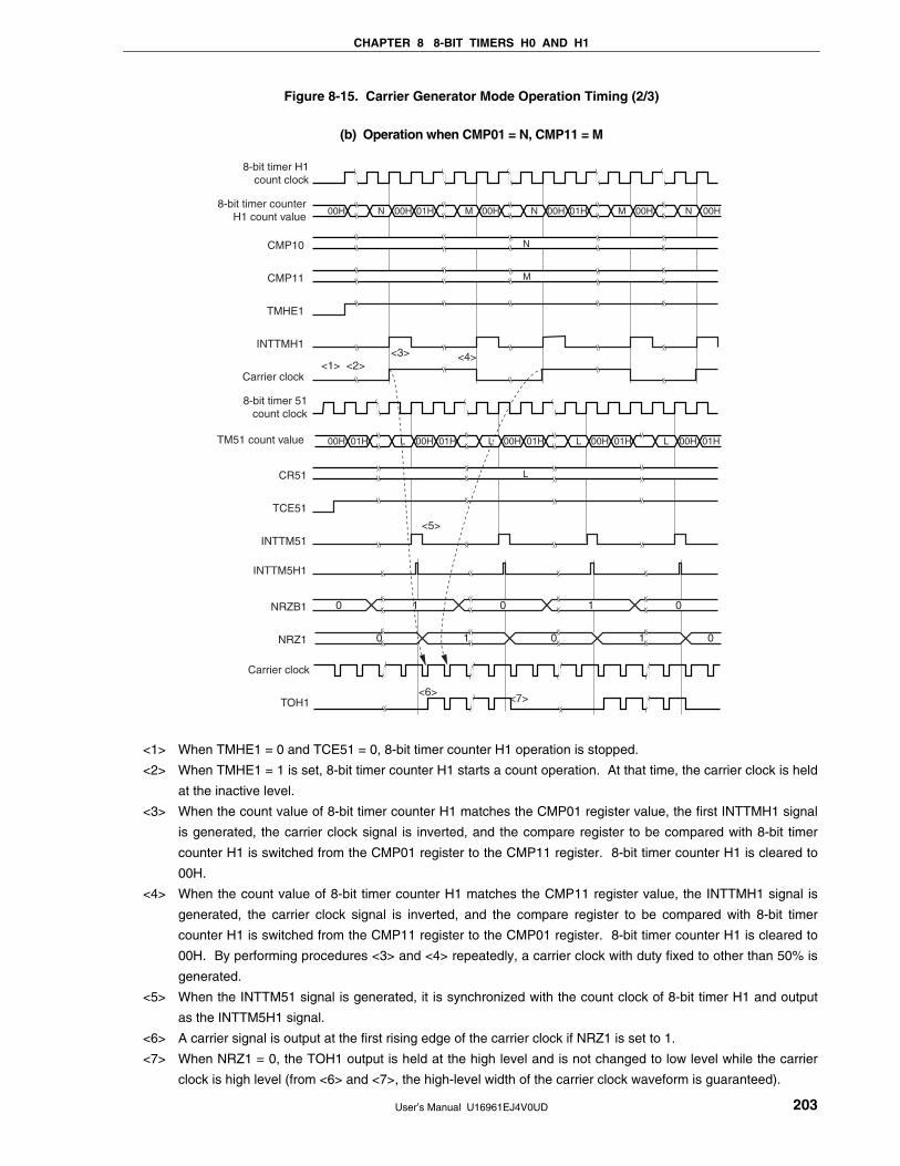
CHAPTER 8 8-BIT TIMERS H0 AND H1
User’s Manual U16961EJ4V0UD 203
Figure 8-15. Carrier Generator Mode Operation Timing (2/3)
(b) Operation when CMP01 = N, CMP11 = M
N
L
CMP10
CMP11
TMHE1
INTTMH1
Carrier clock
TM51 count value
00H N 00H 01H M 00H N 00H 01H M 00H 00HN
M
CR51
TCE51
TOH1
0
0
1
1
0
0
1
1
0
0
INTTM51
NRZB1
NRZ1
Carrier clock
00H 01H L 00H 01H L 00H 01H L 00H 01H 00H 01HL
INTTM5H1
<1> <2><3> <4>
<5>
<6><7>
8-bit timer 51count clock
8-bit timer H1count clock
8-bit timer counterH1 count value
<1> When TMHE1 = 0 and TCE51 = 0, 8-bit timer counter H1 operation is stopped.
<2> When TMHE1 = 1 is set, 8-bit timer counter H1 starts a count operation. At that time, the carrier clock is held
at the inactive level.
<3> When the count value of 8-bit timer counter H1 matches the CMP01 register value, the first INTTMH1 signal
is generated, the carrier clock signal is inverted, and the compare register to be compared with 8-bit timer
counter H1 is switched from the CMP01 register to the CMP11 register. 8-bit timer counter H1 is cleared to
00H.
<4> When the count value of 8-bit timer counter H1 matches the CMP11 register value, the INTTMH1 signal is
generated, the carrier clock signal is inverted, and the compare register to be compared with 8-bit timer
counter H1 is switched from the CMP11 register to the CMP01 register. 8-bit timer counter H1 is cleared to
00H. By performing procedures <3> and <4> repeatedly, a carrier clock with duty fixed to other than 50% is
generated.
<5> When the INTTM51 signal is generated, it is synchronized with the count clock of 8-bit timer H1 and output
as the INTTM5H1 signal.
<6> A carrier signal is output at the first rising edge of the carrier clock if NRZ1 is set to 1.
<7> When NRZ1 = 0, the TOH1 output is held at the high level and is not changed to low level while the carrier
clock is high level (from <6> and <7>, the high-level width of the carrier clock waveform is guaranteed).
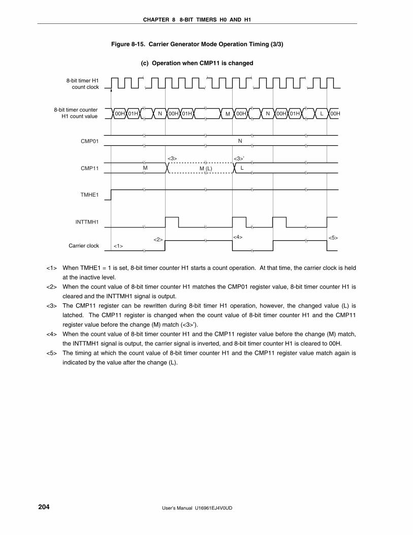
CHAPTER 8 8-BIT TIMERS H0 AND H1
User’s Manual U16961EJ4V0UD 204
Figure 8-15. Carrier Generator Mode Operation Timing (3/3)
(c) Operation when CMP11 is changed
8-bit timer H1
count clock
CMP01
TMHE1
INTTMH1
Carrier clock
00H 01H N 00H 01H 01HM 00H N 00H L 00H
<1>
<3>’
<4>
<3>
<2>
CMP11
<5>
M
N
LM (L)
8-bit timer counterH1 count value
<1> When TMHE1 = 1 is set, 8-bit timer counter H1 starts a count operation. At that time, the carrier clock is held
at the inactive level.
<2> When the count value of 8-bit timer counter H1 matches the CMP01 register value, 8-bit timer counter H1 is
cleared and the INTTMH1 signal is output.
<3> The CMP11 register can be rewritten during 8-bit timer H1 operation, however, the changed value (L) is
latched. The CMP11 register is changed when the count value of 8-bit timer counter H1 and the CMP11
register value before the change (M) match (<3>’).
<4> When the count value of 8-bit timer counter H1 and the CMP11 register value before the change (M) match,
the INTTMH1 signal is output, the carrier signal is inverted, and 8-bit timer counter H1 is cleared to 00H.
<5> The timing at which the count value of 8-bit timer counter H1 and the CMP11 register value match again is
indicated by the value after the change (L).
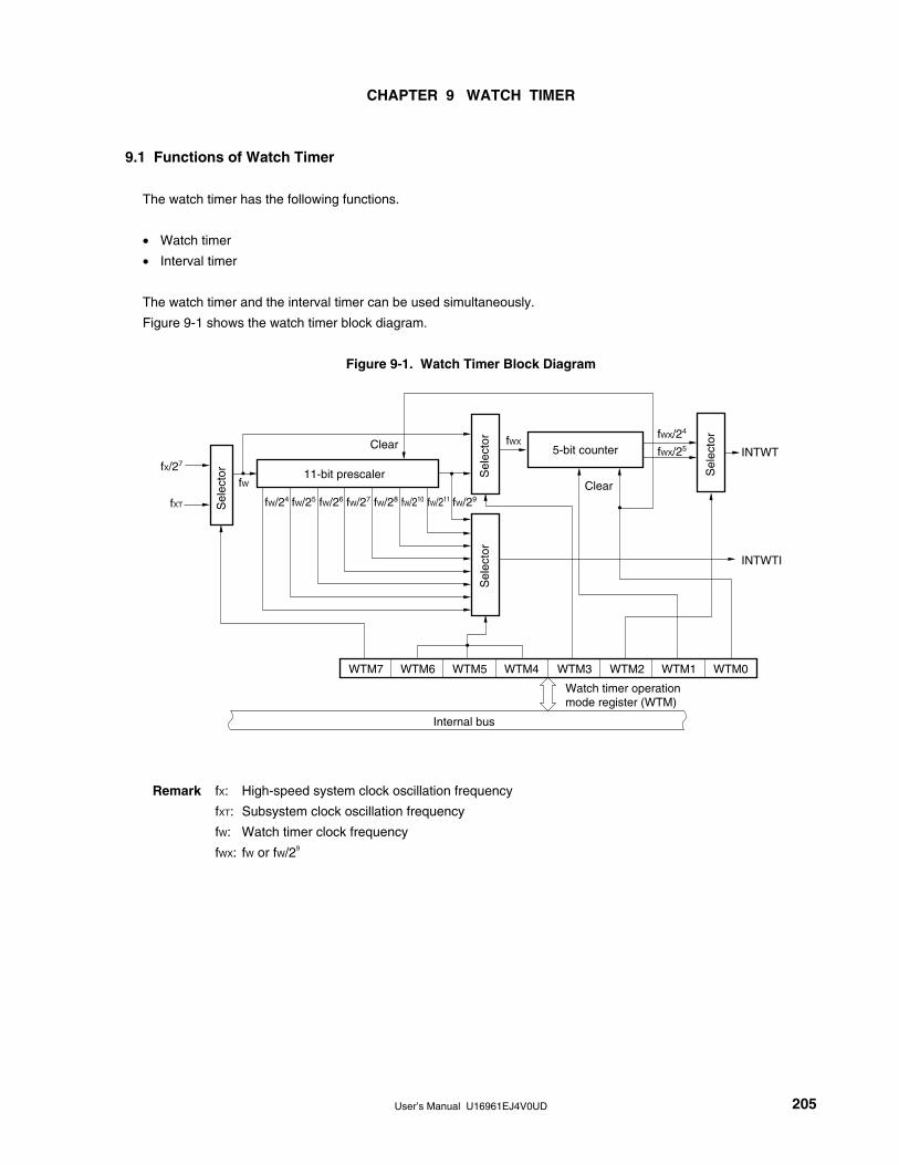
User’s Manual U16961EJ4V0UD 205
CHAPTER 9 WATCH TIMER
9.1 Functions of Watch Timer
The watch timer has the following functions.
• Watch timer
• Interval timer
The watch timer and the interval timer can be used simultaneously.
Figure 9-1 shows the watch timer block diagram.
Figure 9-1. Watch Timer Block Diagram
fX/27
fW/24 fW/25 fW/26 fW/27 fW/28 fW/210 fW/211 fW/29fXT
INTWT
INTWTI
WTM0WTM1WTM2WTM3WTM4WTM5WTM6WTM7
fW
Clear
11-bit prescalerClear
5-bit counter
Watch timer operation mode register (WTM)
Internal bus
Sel
ecto
r
Sel
ecto
r
Sel
ecto
r
Sel
ecto
r fWX/24
fWX/25fWX
Remark fX: High-speed system clock oscillation frequency
fXT: Subsystem clock oscillation frequency
fW: Watch timer clock frequency
fWX: fW or fW/29
CHAPTER 9 WATCH TIMER
User’s Manual U16961EJ4V0UD 206
(1) Watch timer
When the high-speed system clock or subsystem clock is used, interrupt requests (INTWT) are generated at
preset intervals.
Table 9-1. Watch Timer Interrupt Time
Interrupt Time When Operated at fXT = 32.768 kHz When Operated at fX = 10 MHz
24/fW 488 µs 205 µs
25/fW 977 µs 410 µs
213/fW 0.25 s 0.105 s
214/fW 0.5 s 0.210 s
Remark fX: High-speed system clock oscillation frequency
fXT: Subsystem clock oscillation frequency
fW: Watch timer clock frequency
(2) Interval timer
Interrupt requests (INTWTI) are generated at preset time intervals.
Table 9-2. Interval Timer Interval Time
Interval Time When Operated at fXT = 32.768 kHz When Operated at fX = 10 MHz
24/fW 488 µs 205 µs
25/fW 977 µs 410 µs
26/fW 1.95 ms 820 µs
27/fW 3.91 ms 1.64 ms
28/fW 7.81 ms 3.28 ms
29/fW 15.6 ms 6.55 ms
210/fW 31.3 ms 13.1 ms
211/fW 62.5 ms 26.2 ms
Remark fX: High-speed system clock oscillation frequency
fXT: Subsystem clock oscillation frequency
fW: Watch timer clock frequency
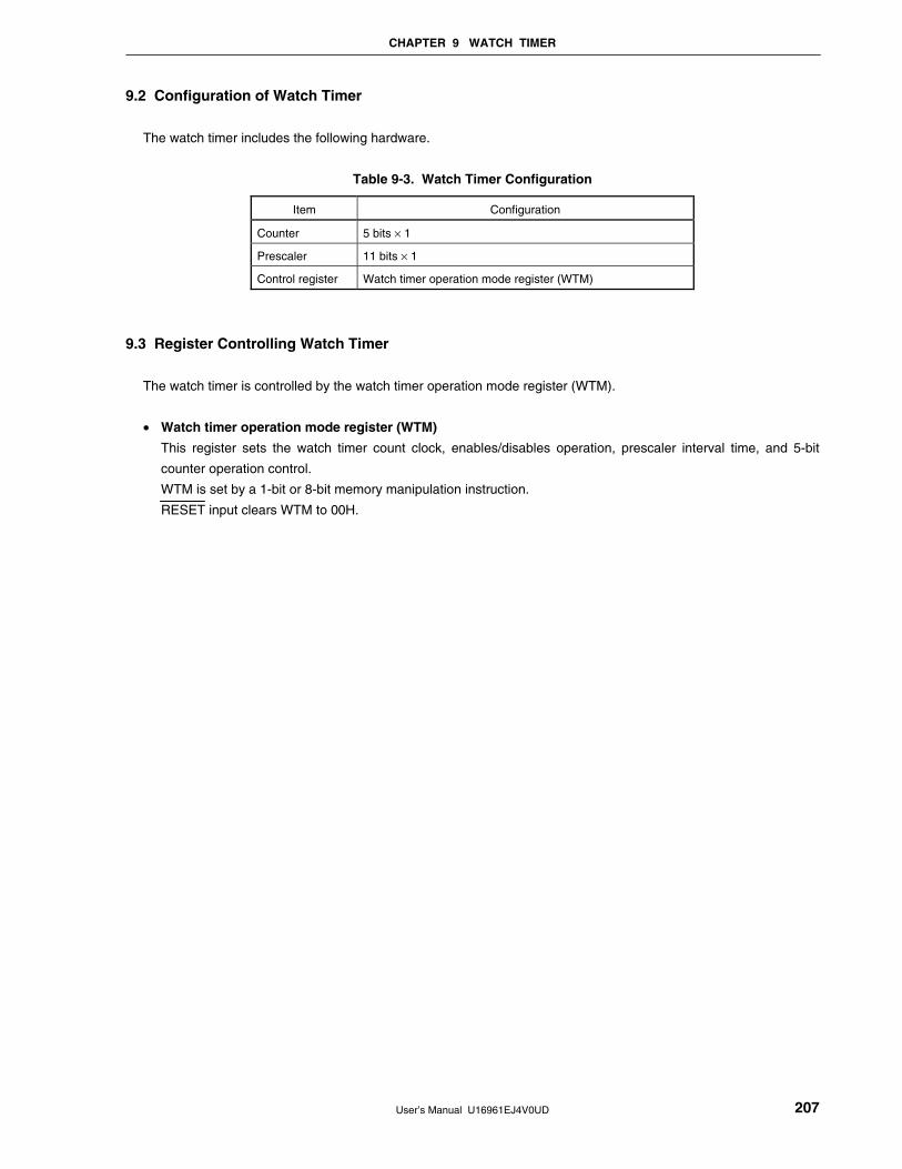
CHAPTER 9 WATCH TIMER
User’s Manual U16961EJ4V0UD 207
9.2 Configuration of Watch Timer
The watch timer includes the following hardware.
Table 9-3. Watch Timer Configuration
Item Configuration
Counter 5 bits × 1
Prescaler 11 bits × 1
Control register Watch timer operation mode register (WTM)
9.3 Register Controlling Watch Timer
The watch timer is controlled by the watch timer operation mode register (WTM).
• Watch timer operation mode register (WTM)
This register sets the watch timer count clock, enables/disables operation, prescaler interval time, and 5-bit
counter operation control.
WTM is set by a 1-bit or 8-bit memory manipulation instruction.
RESET input clears WTM to 00H.
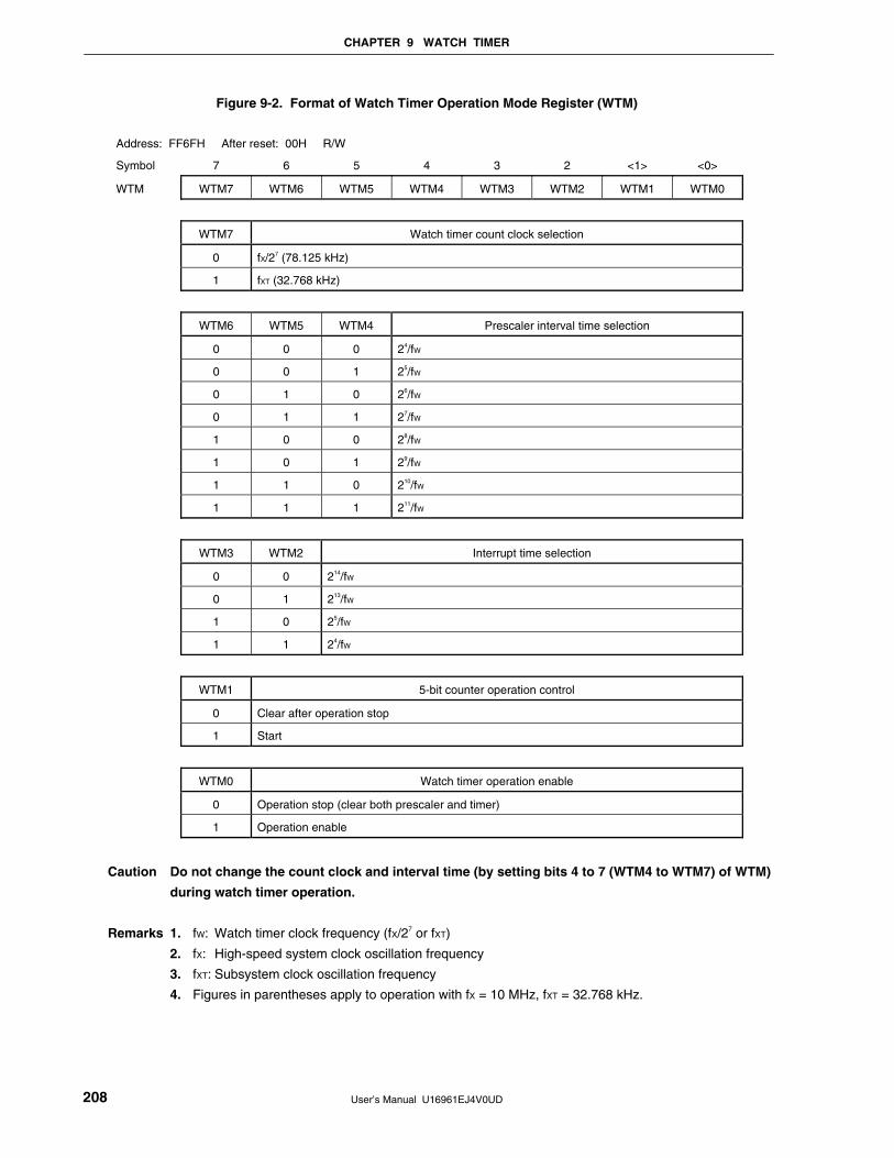
CHAPTER 9 WATCH TIMER
User’s Manual U16961EJ4V0UD 208
Figure 9-2. Format of Watch Timer Operation Mode Register (WTM)
Address: FF6FH After reset: 00H R/W
Symbol 7 6 5 4 3 2 <1> <0>
WTM WTM7 WTM6 WTM5 WTM4 WTM3 WTM2 WTM1 WTM0
WTM7 Watch timer count clock selection
0 fX/27 (78.125 kHz)
1 fXT (32.768 kHz)
WTM6 WTM5 WTM4 Prescaler interval time selection
0 0 0 24/fW
0 0 1 25/fW
0 1 0 26/fW
0 1 1 27/fW
1 0 0 28/fW
1 0 1 29/fW
1 1 0 210/fW
1 1 1 211/fW
WTM3 WTM2 Interrupt time selection
0 0 214/fW
0 1 213/fW
1 0 25/fW
1 1 24/fW
WTM1 5-bit counter operation control
0 Clear after operation stop
1 Start
WTM0 Watch timer operation enable
0 Operation stop (clear both prescaler and timer)
1 Operation enable
Caution Do not change the count clock and interval time (by setting bits 4 to 7 (WTM4 to WTM7) of WTM)
during watch timer operation.
Remarks 1. fW: Watch timer clock frequency (fX/27 or fXT)
2. fX: High-speed system clock oscillation frequency
3. fXT: Subsystem clock oscillation frequency
4. Figures in parentheses apply to operation with fX = 10 MHz, fXT = 32.768 kHz.
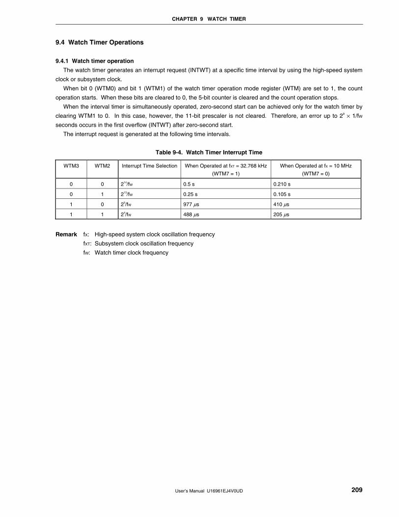
CHAPTER 9 WATCH TIMER
User’s Manual U16961EJ4V0UD 209
9.4 Watch Timer Operations
9.4.1 Watch timer operation
The watch timer generates an interrupt request (INTWT) at a specific time interval by using the high-speed system
clock or subsystem clock.
When bit 0 (WTM0) and bit 1 (WTM1) of the watch timer operation mode register (WTM) are set to 1, the count
operation starts. When these bits are cleared to 0, the 5-bit counter is cleared and the count operation stops.
When the interval timer is simultaneously operated, zero-second start can be achieved only for the watch timer by
clearing WTM1 to 0. In this case, however, the 11-bit prescaler is not cleared. Therefore, an error up to 29 × 1/fW
seconds occurs in the first overflow (INTWT) after zero-second start.
The interrupt request is generated at the following time intervals.
Table 9-4. Watch Timer Interrupt Time
WTM3 WTM2 Interrupt Time Selection When Operated at fXT = 32.768 kHz
(WTM7 = 1)
When Operated at fX = 10 MHz
(WTM7 = 0)
0 0 214/fW 0.5 s 0.210 s
0 1 213/fW 0.25 s 0.105 s
1 0 25/fW 977 µs 410 µs
1 1 24/fW 488 µs 205 µs
Remark fX: High-speed system clock oscillation frequency
fXT: Subsystem clock oscillation frequency
fW: Watch timer clock frequency
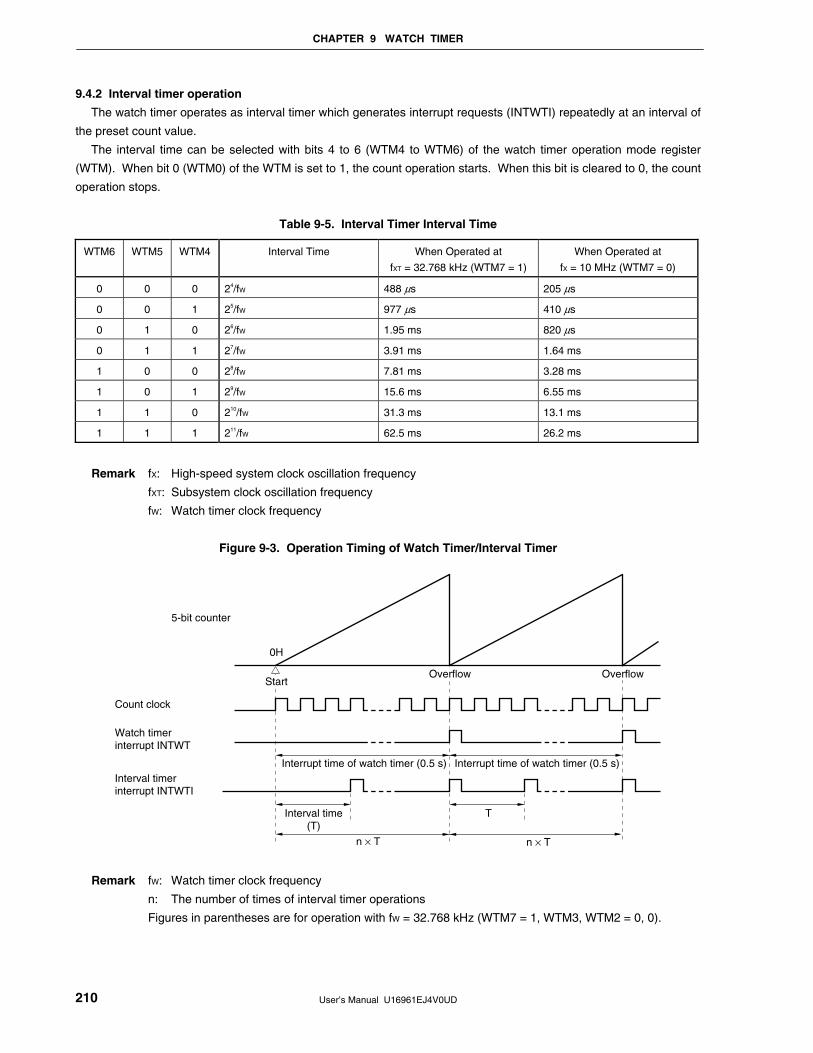
CHAPTER 9 WATCH TIMER
User’s Manual U16961EJ4V0UD 210
9.4.2 Interval timer operation
The watch timer operates as interval timer which generates interrupt requests (INTWTI) repeatedly at an interval of
the preset count value.
The interval time can be selected with bits 4 to 6 (WTM4 to WTM6) of the watch timer operation mode register
(WTM). When bit 0 (WTM0) of the WTM is set to 1, the count operation starts. When this bit is cleared to 0, the count
operation stops.
Table 9-5. Interval Timer Interval Time
WTM6 WTM5 WTM4 Interval Time When Operated at
fXT = 32.768 kHz (WTM7 = 1)
When Operated at
fX = 10 MHz (WTM7 = 0)
0 0 0 24/fW 488 µs 205 µs
0 0 1 25/fW 977 µs 410 µs
0 1 0 26/fW 1.95 ms 820 µs
0 1 1 27/fW 3.91 ms 1.64 ms
1 0 0 28/fW 7.81 ms 3.28 ms
1 0 1 29/fW 15.6 ms 6.55 ms
1 1 0 210/fW 31.3 ms 13.1 ms
1 1 1 211/fW 62.5 ms 26.2 ms
Remark fX: High-speed system clock oscillation frequency
fXT: Subsystem clock oscillation frequency
fW: Watch timer clock frequency
Figure 9-3. Operation Timing of Watch Timer/Interval Timer
0H
StartOverflow Overflow
5-bit counter
Count clock
Watch timerinterrupt INTWT
Interval timerinterrupt INTWTI
Interrupt time of watch timer (0.5 s)
Interval time(T)
T
Interrupt time of watch timer (0.5 s)
n × T n × T
Remark fW: Watch timer clock frequency
n: The number of times of interval timer operations
Figures in parentheses are for operation with fW = 32.768 kHz (WTM7 = 1, WTM3, WTM2 = 0, 0).
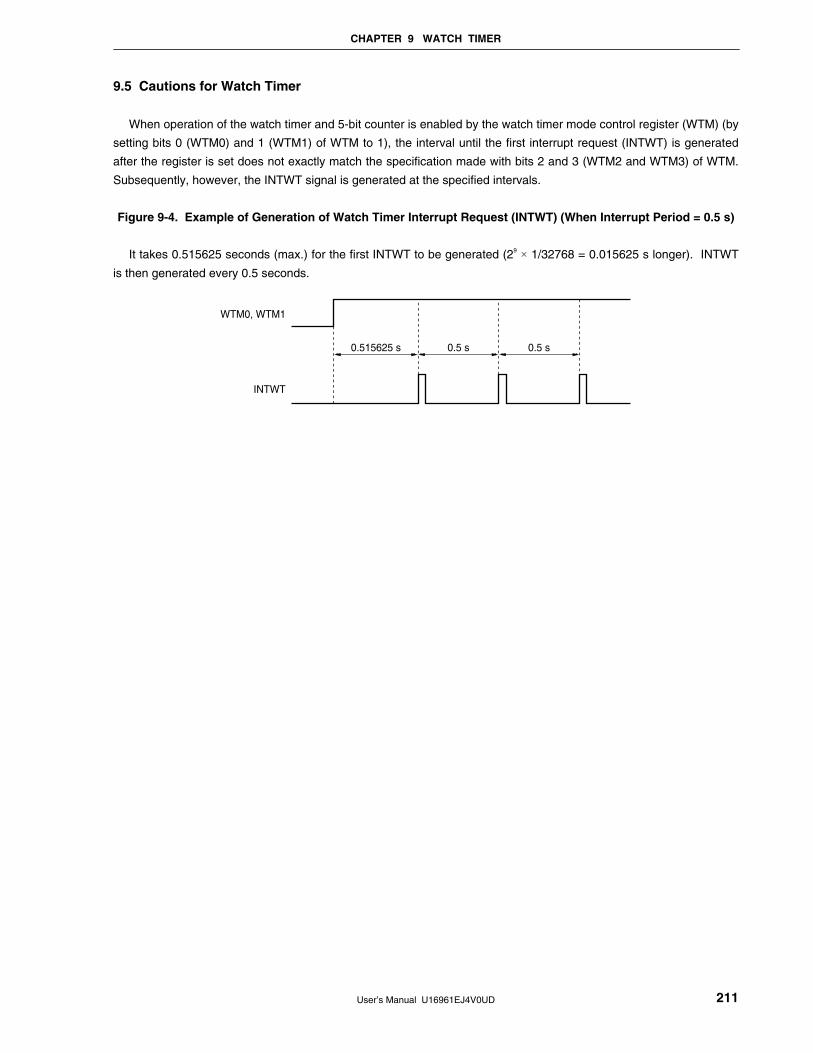
CHAPTER 9 WATCH TIMER
User’s Manual U16961EJ4V0UD 211
9.5 Cautions for Watch Timer
When operation of the watch timer and 5-bit counter is enabled by the watch timer mode control register (WTM) (by
setting bits 0 (WTM0) and 1 (WTM1) of WTM to 1), the interval until the first interrupt request (INTWT) is generated
after the register is set does not exactly match the specification made with bits 2 and 3 (WTM2 and WTM3) of WTM.
Subsequently, however, the INTWT signal is generated at the specified intervals.
Figure 9-4. Example of Generation of Watch Timer Interrupt Request (INTWT) (When Interrupt Period = 0.5 s)
It takes 0.515625 seconds (max.) for the first INTWT to be generated (29 × 1/32768 = 0.015625 s longer). INTWT
is then generated every 0.5 seconds.
0.5 s0.5 s0.515625 s
WTM0, WTM1
INTWT
User’s Manual U16961EJ4V0UD 212
CHAPTER 10 WATCHDOG TIMER 10.1 Functions of Watchdog Timer
The watchdog timer is used to detect an inadvertent program loop. If a program loop is detected, an internal reset signal is generated.
When a reset occurs due to the watchdog timer, bit 4 (WDTRF) of the reset control flag register (RESF) is set to 1. For details of RESF, refer to CHAPTER 18 RESET FUNCTION.
Table 10-1. Loop Detection Time of Watchdog Timer
Loop Detection Time
During Internal Oscillation Clock Operation During High-Speed System Clock Operation
211/fR (4.27 ms) 213/fXP (819.2 μs)
212/fR (8.53 ms) 214/fXP (1.64 ms)
213/fR (17.07 ms) 215/fXP (3.28 ms)
214/fR (34.13 ms) 216/fXP (6.55 ms)
215/fR (68.27 ms) 217/fXP (13.11 ms)
216/fR (136.53 ms) 218/fXP (26.21 ms)
217/fR (273.07 ms) 219/fXP (52.43 ms)
218/fR (546.13 ms) 220/fXP (104.86 ms)
Remarks 1. fR: Internal oscillation clock oscillation frequency 2. fXP: High-speed system clock oscillation frequency 3. Figures in parentheses apply to operation at fR = 480 kHz (MAX.), fXP = 10 MHz
The operation mode of the watchdog timer (WDT) is switched according to the option byte setting of the on-chip
internal oscillator as shown in Table 10-2.
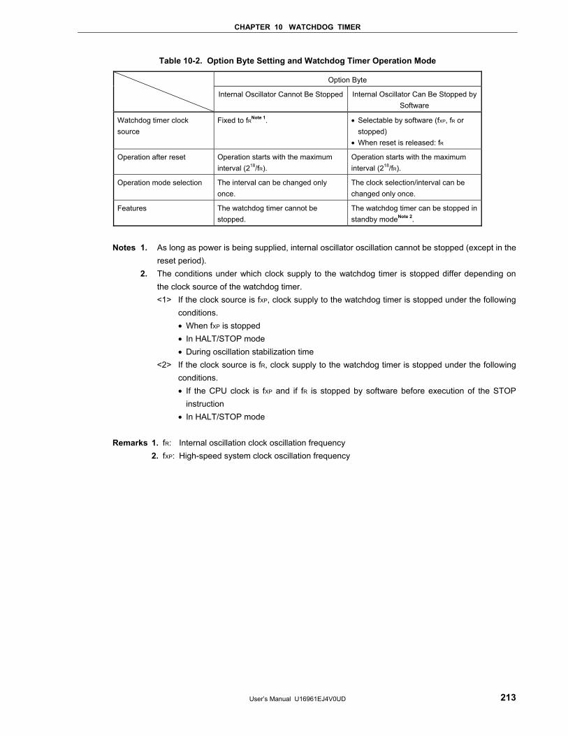
CHAPTER 10 WATCHDOG TIMER
User’s Manual U16961EJ4V0UD 213
Table 10-2. Option Byte Setting and Watchdog Timer Operation Mode
Option Byte
Internal Oscillator Cannot Be Stopped Internal Oscillator Can Be Stopped by Software
Watchdog timer clock source
Fixed to fRNote 1. • Selectable by software (fXP, fR or stopped) • When reset is released: fR
Operation after reset Operation starts with the maximum interval (218/fR).
Operation starts with the maximum interval (218/fR).
Operation mode selection The interval can be changed only once.
The clock selection/interval can be changed only once.
Features The watchdog timer cannot be stopped.
The watchdog timer can be stopped in standby modeNote 2.
Notes 1. As long as power is being supplied, internal oscillator oscillation cannot be stopped (except in the
reset period). 2. The conditions under which clock supply to the watchdog timer is stopped differ depending on
the clock source of the watchdog timer. <1> If the clock source is fXP, clock supply to the watchdog timer is stopped under the following
conditions. • When fXP is stopped • In HALT/STOP mode • During oscillation stabilization time
<2> If the clock source is fR, clock supply to the watchdog timer is stopped under the following conditions. • If the CPU clock is fXP and if fR is stopped by software before execution of the STOP
instruction • In HALT/STOP mode
Remarks 1. fR: Internal oscillation clock oscillation frequency 2. fXP: High-speed system clock oscillation frequency
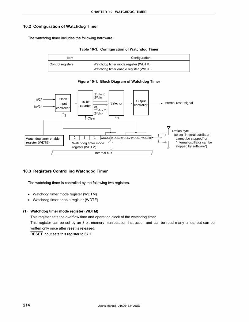
CHAPTER 10 WATCHDOG TIMER
User’s Manual U16961EJ4V0UD 214
10.2 Configuration of Watchdog Timer
The watchdog timer includes the following hardware.
Table 10-3. Configuration of Watchdog Timer
Item Configuration
Control registers Watchdog timer mode register (WDTM) Watchdog timer enable register (WDTE)
Figure 10-1. Block Diagram of Watchdog Timer
fR/22 Clock input
controller
Outputcontroller
Internal reset signal
WDCS2
Internal bus
WDCS1 WDCS0
fXP/24
WDCS3WDCS40 1 1
Selector16-bitcounter
Watchdog timer enableregister (WDTE) Watchdog timer mode
register (WDTM)
32
Clear
Option byte (to set “internal oscillator cannot be stopped” or “internal oscillator can be stopped by software”)
or213/fXP to 220/fXP
211/fR to218/fR
10.3 Registers Controlling Watchdog Timer
The watchdog timer is controlled by the following two registers. • Watchdog timer mode register (WDTM) • Watchdog timer enable register (WDTE)
(1) Watchdog timer mode register (WDTM)
This register sets the overflow time and operation clock of the watchdog timer. This register can be set by an 8-bit memory manipulation instruction and can be read many times, but can be written only once after reset is released. RESET input sets this register to 67H.

CHAPTER 10 WATCHDOG TIMER
User’s Manual U16961EJ4V0UD 215
Figure 10-2. Format of Watchdog Timer Mode Register (WDTM)
0
WDCS0
1
WDCS1
2
WDCS2
3
WDCS3
4
WDCS4
5
1
6
1
7
0
Symbol
WDTM
Address: FF98H After reset: 67H R/W
WDCS4Note 1 WDCS3Note 1 Operation clock selection
0 0 Internal oscillation clock (fR)
0 1 High-speed system clock (fXP)
1 × Watchdog timer operation stopped
Overflow time setting WDCS2Note 2 WDCS1Note 2 WDCS0Note 2
During internal oscillation clock operation
During high-speed system clock operation
0 0 0 211/fR (4.27 ms) 213/fXP (819.2 μs)
0 0 1 212/fR (8.53 ms) 214/fXP (1.64 ms)
0 1 0 213/fR (17.07 ms) 215/fXP (3.28 ms)
0 1 1 214/fR (34.13 ms) 216/fXP (6.55 ms)
1 0 0 215/fR (68.27 ms) 217/fXP (13.11 ms)
1 0 1 216/fR (136.53 ms) 218/fXP (26.21 ms)
1 1 0 217/fR (273.07 ms) 219/fXP (52.43 ms)
1 1 1 218/fR (546.13 ms) 220/fXP (104.86 ms)
Notes 1. If “internal oscillator cannot be stopped” is specified by the option byte, this cannot be set. The internal oscillation clock will be selected no matter what value is written.
2. Reset is released at the maximum cycle (WDCS2, 1, 0 = 1, 1, 1).
Cautions 1. If data is written to WDTM, a wait cycle is generated. Do not write data to WDTM when the CPU is operating on the subsystem clock and the high-speed system clock is stopped. For details, see CHAPTER 29 CAUTIONS FOR WAIT.
2. Set bits 7, 6, and 5 to 0, 1, and 1, respectively (when “internal oscillator cannot be stopped” is selected by the option byte, other values are ignored).
3. After reset is released, WDTM can be written only once by an 8-bit memory manipulation instruction. If writing is attempted a second time, an internal reset signal is generated. If the source clock to the watchdog timer is stopped, however, an internal reset signal is generated when the source clock to the watchdog timer resumes operation.
4. WDTM cannot be set by a 1-bit memory manipulation instruction. 5. If “internal oscillator can be stopped by software” is selected by the option byte and
the watchdog timer is stopped by setting WDCS4 to 1, the watchdog timer does not resume operation even if WDCS4 is cleared to 0. In addition, the internal reset signal is not generated.
Remarks 1. fR: Internal oscillation clock oscillation frequency 2. fXP: High-speed system clock oscillation frequency 3. ×: Don’t care 4. Figures in parentheses apply to operation at fR = 480 kHz (MAX.), fXP = 10 MHz
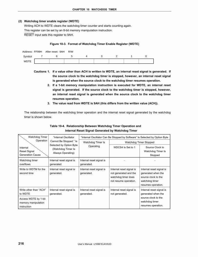
CHAPTER 10 WATCHDOG TIMER
User’s Manual U16961EJ4V0UD 216
(2) Watchdog timer enable register (WDTE) Writing ACH to WDTE clears the watchdog timer counter and starts counting again. This register can be set by an 8-bit memory manipulation instruction. RESET input sets this register to 9AH.
Figure 10-3. Format of Watchdog Timer Enable Register (WDTE)
01234567Symbol
WDTE
Address: FF99H After reset: 9AH R/W
Cautions 1. If a value other than ACH is written to WDTE, an internal reset signal is generated. If the source clock to the watchdog timer is stopped, however, an internal reset signal is generated when the source clock to the watchdog timer resumes operation.
2. If a 1-bit memory manipulation instruction is executed for WDTE, an internal reset signal is generated. If the source clock to the watchdog timer is stopped, however, an internal reset signal is generated when the source clock to the watchdog timer resumes operation.
3. The value read from WDTE is 9AH (this differs from the written value (ACH)).
The relationship between the watchdog timer operation and the internal reset signal generated by the watchdog timer is shown below.
Table 10-4. Relationship Between Watchdog Timer Operation and Internal Reset Signal Generated by Watchdog Timer
“Internal Oscillator Can Be Stopped by Software” Is Selected by Option Byte
Watchdog Timer Stopped
Watchdog Timer Operation Internal Reset Signal Generation Cause
“Internal Oscillator Cannot Be Stopped ” Is Selected by Option Byte
(Watchdog Timer Is Always Operating)
Watchdog Timer Is Operating WDCS4 Is Set to 1 Source Clock to
Watchdog Timer Is Stopped
Watchdog timer overflows
Internal reset signal is generated.
Internal reset signal is generated.
− −
Write to WDTM for the second time
Internal reset signal is generated.
Internal reset signal is generated.
Internal reset signal is not generated and the watchdog timer does not resume operation.
Internal reset signal is generated when the source clock to the watchdog timer resumes operation.
Write other than “ACH” to WDTE
Access WDTE by 1-bit memory manipulation instruction
Internal reset signal is generated.
Internal reset signal is generated.
Internal reset signal is not generated.
Internal reset signal is generated when the source clock to the watchdog timer resumes operation.
CHAPTER 10 WATCHDOG TIMER
User’s Manual U16961EJ4V0UD 217
10.4 Operation of Watchdog Timer 10.4.1 Watchdog timer operation when “internal oscillator cannot be stopped” is selected by option byte
The operation clock of watchdog timer is fixed to the internal oscillation clock. After reset is released, operation is started at the maximum cycle (bits 2, 1, and 0 (WDCS2, WDCS1, WDCS0) of
the watchdog timer mode register (WDTM) = 1, 1, 1). The watchdog timer operation cannot be stopped.
The following shows the watchdog timer operation after reset release.
1. The status after reset release is as follows. • Operation clock: Internal oscillation clock • Cycle: 218/fR (546.13 ms: At operation with fR = 480 kHz (MAX.)) • Counting starts 2. The following should be set in the watchdog timer mode register (WDTM) by an 8-bit memory manipulation
instructionNotes 1, 2. • Cycle: Set using bits 2 to 0 (WDCS2 to WDCS0) 3. After the above procedures are executed, writing ACH to WDTE clears the count to 0, enabling recounting.
Notes 1. The operation clock (internal oscillation clock) cannot be changed. If any value is written to bits 3 and
4 (WDCS3, WDCS4) of WDTM, it is ignored. 2. As soon as WDTM is written, the counter of the watchdog timer is cleared.
Caution In this mode, operation of the watchdog timer absolutely cannot be stopped even during STOP
instruction execution. For 8-bit timer H1 (TMH1), a division of the internal oscillation clock can be selected as the count source, so clear the watchdog timer using the interrupt request of TMH1 before the watchdog timer overflows after STOP instruction execution. If this processing is not performed, an internal reset signal is generated when the watchdog timer overflows after STOP instruction execution.
CHAPTER 10 WATCHDOG TIMER
User’s Manual U16961EJ4V0UD 218
10.4.2 Watchdog timer operation when “internal oscillator can be stopped by software” is selected by option byte
The operation clock of the watchdog timer can be selected as either the internal oscillation clock or the high-speed system clock.
After reset is released, operation is started at the maximum cycle (bits 2, 1, and 0 (WDCS2, WDCS1, WDCS0) of the watchdog timer mode register (WDTM) = 1, 1, 1).
The following shows the watchdog timer operation after reset release. 1. The status after reset release is as follows. • Operation clock: Internal oscillation clock • Cycle: 218/fR (546.13 ms: At operation with fR = 480 kHz (MAX.)) • Counting starts 2. The following should be set in the watchdog timer mode register (WDTM) by an 8-bit memory manipulation
instructionNotes 1, 2, 3. • Operation clock: Any of the following can be selected using bits 3 and 4 (WDCS3 and WDCS4). Internal oscillation clock (fR) High-speed system clock (fXP) Watchdog timer operation stopped • Cycle: Set using bits 2 to 0 (WDCS2 to WDCS0) 3. After the above procedures are executed, writing ACH to WDTE clears the count to 0, enabling recounting.
Notes 1. As soon as WDTM is written, the counter of the watchdog timer is cleared. 2. Set bits 7, 6, and 5 to 0, 1, 1, respectively. Do not set the other values. 3. If the watchdog timer is stopped by setting WDCS4 and WDCS3 to 1 and ×, respectively, an internal
reset signal is not generated even if the following processing is performed. • WDTM is written a second time. • A 1-bit memory manipulation instruction is executed to WDTE. • A value other than ACH is written to WDTE.
Caution In this mode, watchdog timer operation is stopped during HALT/STOP instruction execution.
After HALT/STOP mode is released, counting is started again using the operation clock of the watchdog timer set before HALT/STOP instruction execution by WDTM. At this time, the counter is not cleared to 0 but holds its value.
For the watchdog timer operation during STOP mode and HALT mode in each status, refer to 10.4.3 Watchdog timer operation in STOP mode and 10.4.4 Watchdog timer operation in HALT mode.
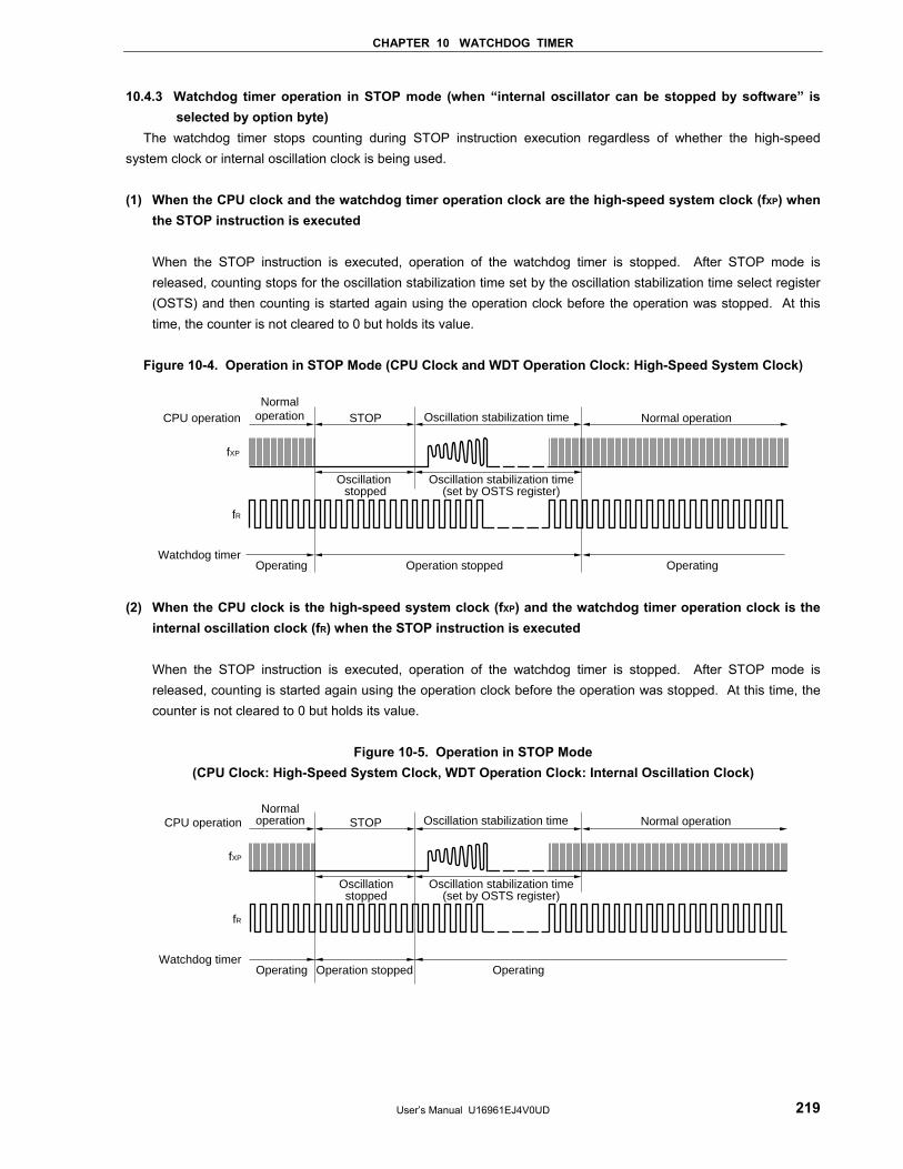
CHAPTER 10 WATCHDOG TIMER
User’s Manual U16961EJ4V0UD 219
10.4.3 Watchdog timer operation in STOP mode (when “internal oscillator can be stopped by software” is selected by option byte)
The watchdog timer stops counting during STOP instruction execution regardless of whether the high-speed system clock or internal oscillation clock is being used. (1) When the CPU clock and the watchdog timer operation clock are the high-speed system clock (fXP) when
the STOP instruction is executed
When the STOP instruction is executed, operation of the watchdog timer is stopped. After STOP mode is released, counting stops for the oscillation stabilization time set by the oscillation stabilization time select register (OSTS) and then counting is started again using the operation clock before the operation was stopped. At this time, the counter is not cleared to 0 but holds its value.
Figure 10-4. Operation in STOP Mode (CPU Clock and WDT Operation Clock: High-Speed System Clock)
Watchdog timerOperating Operation stopped Operating
fR
fXP
CPU operationNormal
operation STOP Oscillation stabilization time Normal operation
Oscillation stopped
Oscillation stabilization time(set by OSTS register)
(2) When the CPU clock is the high-speed system clock (fXP) and the watchdog timer operation clock is the
internal oscillation clock (fR) when the STOP instruction is executed
When the STOP instruction is executed, operation of the watchdog timer is stopped. After STOP mode is released, counting is started again using the operation clock before the operation was stopped. At this time, the counter is not cleared to 0 but holds its value.
Figure 10-5. Operation in STOP Mode
(CPU Clock: High-Speed System Clock, WDT Operation Clock: Internal Oscillation Clock)
Watchdog timerOperating
fR
fXP
CPU operationNormal
operation STOP Oscillation stabilization time Normal operation
Oscillationstopped
Oscillation stabilization time(set by OSTS register)
Operating Operation stopped
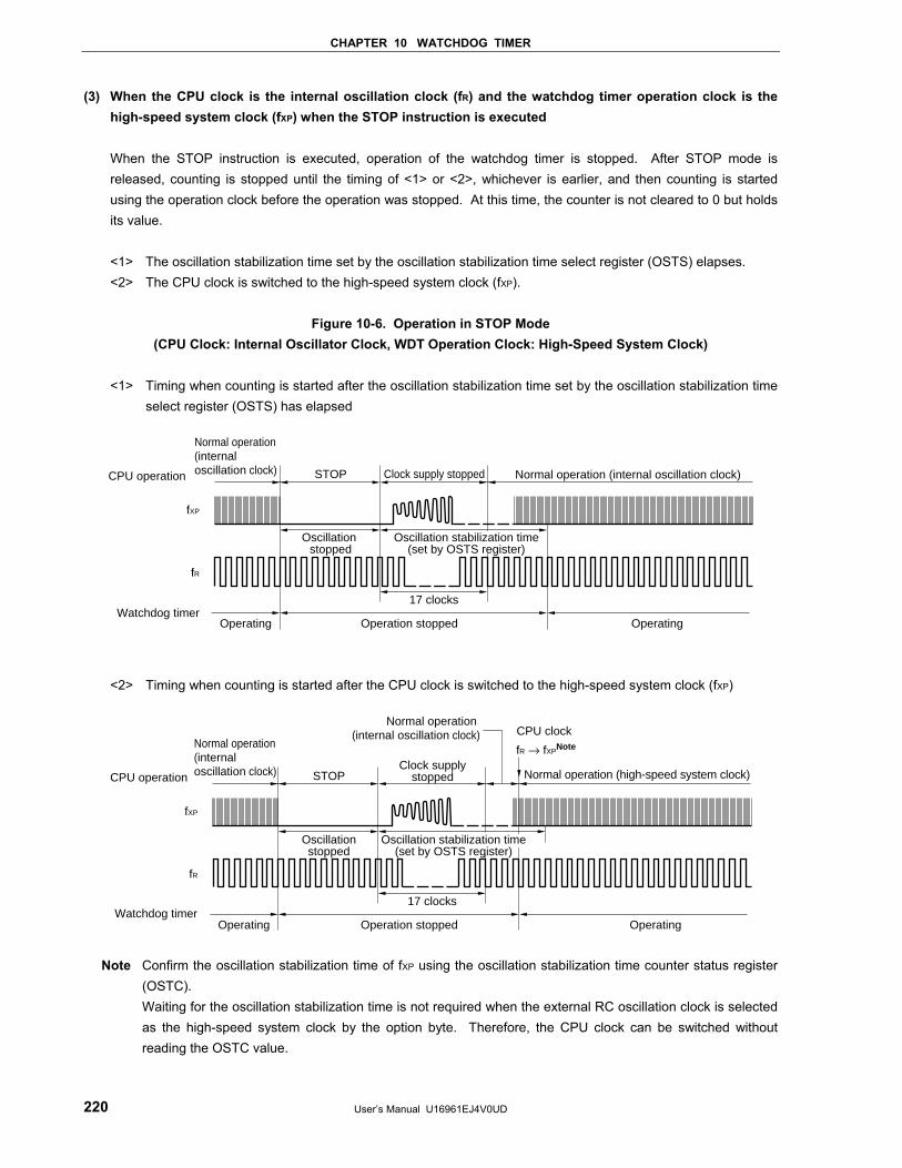
CHAPTER 10 WATCHDOG TIMER
User’s Manual U16961EJ4V0UD 220
(3) When the CPU clock is the internal oscillation clock (fR) and the watchdog timer operation clock is the high-speed system clock (fXP) when the STOP instruction is executed
When the STOP instruction is executed, operation of the watchdog timer is stopped. After STOP mode is released, counting is stopped until the timing of <1> or <2>, whichever is earlier, and then counting is started using the operation clock before the operation was stopped. At this time, the counter is not cleared to 0 but holds its value. <1> The oscillation stabilization time set by the oscillation stabilization time select register (OSTS) elapses. <2> The CPU clock is switched to the high-speed system clock (fXP).
Figure 10-6. Operation in STOP Mode
(CPU Clock: Internal Oscillator Clock, WDT Operation Clock: High-Speed System Clock)
<1> Timing when counting is started after the oscillation stabilization time set by the oscillation stabilization time select register (OSTS) has elapsed
Watchdog timerOperating Operation stopped Operating
fR
fXP
CPU operation
17 clocks
Normal operation(internal oscillation clock) Clock supply stopped Normal operation (internal oscillation clock)
Oscillation stopped
STOP
Oscillation stabilization time(set by OSTS register)
<2> Timing when counting is started after the CPU clock is switched to the high-speed system clock (fXP)
Operating Operation stopped Operating
fR
fXP
fR → fXPNote
CPU operation
17 clocks
Normal operation(internal oscillation clock) Clock supply
stopped
Normal operation (internal oscillation clock)
Normal operation (high-speed system clock)
CPU clock
Oscillationstopped
STOP
Oscillation stabilization time(set by OSTS register)
Watchdog timer
Note Confirm the oscillation stabilization time of fXP using the oscillation stabilization time counter status register
(OSTC). Waiting for the oscillation stabilization time is not required when the external RC oscillation clock is selected
as the high-speed system clock by the option byte. Therefore, the CPU clock can be switched without reading the OSTC value.
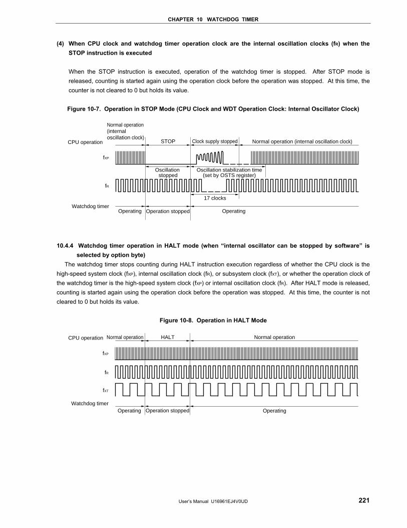
CHAPTER 10 WATCHDOG TIMER
User’s Manual U16961EJ4V0UD 221
(4) When CPU clock and watchdog timer operation clock are the internal oscillation clocks (fR) when the STOP instruction is executed
When the STOP instruction is executed, operation of the watchdog timer is stopped. After STOP mode is released, counting is started again using the operation clock before the operation was stopped. At this time, the counter is not cleared to 0 but holds its value.
Figure 10-7. Operation in STOP Mode (CPU Clock and WDT Operation Clock: Internal Oscillator Clock)
Watchdog timerOperating
fR
fXP
CPU operation
17 clocks
Normal operation(internal oscillation clock)
Clock supply stopped Normal operation (internal oscillation clock)
Oscillation stopped
STOP
Oscillation stabilization time(set by OSTS register)
Operating Operation stopped
10.4.4 Watchdog timer operation in HALT mode (when “internal oscillator can be stopped by software” is
selected by option byte) The watchdog timer stops counting during HALT instruction execution regardless of whether the CPU clock is the
high-speed system clock (fXP), internal oscillation clock (fR), or subsystem clock (fXT), or whether the operation clock of the watchdog timer is the high-speed system clock (fXP) or internal oscillation clock (fR). After HALT mode is released, counting is started again using the operation clock before the operation was stopped. At this time, the counter is not cleared to 0 but holds its value.
Figure 10-8. Operation in HALT Mode
Watchdog timerOperating
fR
fXP
CPU operation Normal operation
Operating
HALT
Operation stopped
fXT
Normal operation
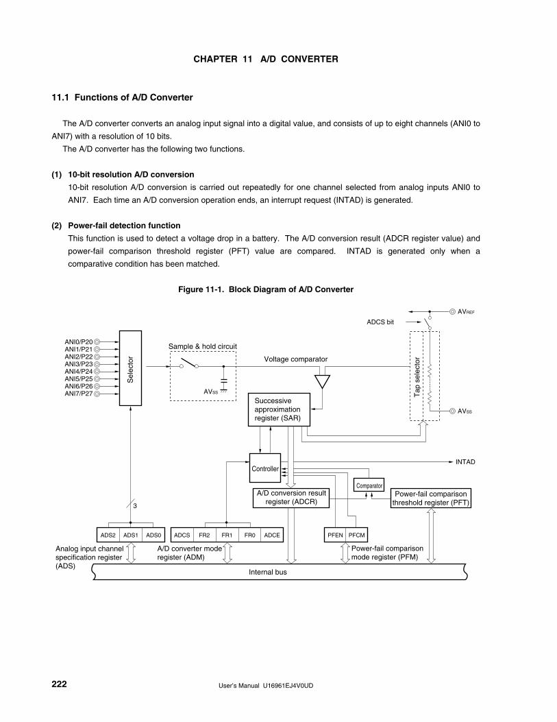
User’s Manual U16961EJ4V0UD 222
CHAPTER 11 A/D CONVERTER
11.1 Functions of A/D Converter
The A/D converter converts an analog input signal into a digital value, and consists of up to eight channels (ANI0 to
ANI7) with a resolution of 10 bits.
The A/D converter has the following two functions.
(1) 10-bit resolution A/D conversion
10-bit resolution A/D conversion is carried out repeatedly for one channel selected from analog inputs ANI0 to
ANI7. Each time an A/D conversion operation ends, an interrupt request (INTAD) is generated.
(2) Power-fail detection function
This function is used to detect a voltage drop in a battery. The A/D conversion result (ADCR register value) and
power-fail comparison threshold register (PFT) value are compared. INTAD is generated only when a
comparative condition has been matched.
Figure 11-1. Block Diagram of A/D Converter
AVREF
AVSS
INTAD
ADCS bit
3
ADS2 ADS1 ADS0 ADCS FR2 FR1 ADCEFR0
Sample & hold circuit
AVSS
Voltage comparator
Controller
A/D conversion resultregister (ADCR)
Power-fail comparisonthreshold register (PFT)
Analog input channelspecification register(ADS)
A/D converter mode register (ADM)
PFEN PFCM
Power-fail comparison mode register (PFM)
Internal bus
Comparator
ANI0/P20ANI1/P21ANI2/P22ANI3/P23ANI4/P24ANI5/P25ANI6/P26ANI7/P27
Successive approximation register (SAR)
Sel
ecto
r
Tap
sel
ecto
r
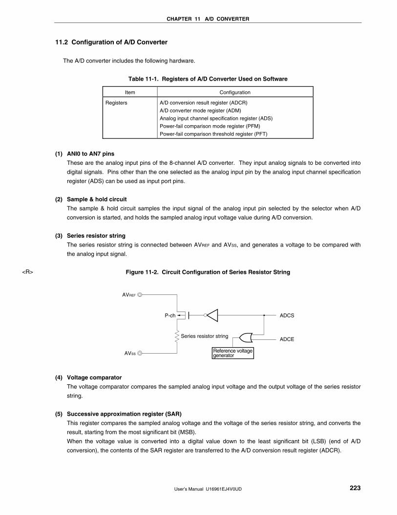
CHAPTER 11 A/D CONVERTER
User’s Manual U16961EJ4V0UD 223
11.2 Configuration of A/D Converter
The A/D converter includes the following hardware.
Table 11-1. Registers of A/D Converter Used on Software
Item Configuration
Registers A/D conversion result register (ADCR)
A/D converter mode register (ADM)
Analog input channel specification register (ADS)
Power-fail comparison mode register (PFM)
Power-fail comparison threshold register (PFT)
(1) ANI0 to AN7 pins
These are the analog input pins of the 8-channel A/D converter. They input analog signals to be converted into
digital signals. Pins other than the one selected as the analog input pin by the analog input channel specification
register (ADS) can be used as input port pins.
(2) Sample & hold circuit
The sample & hold circuit samples the input signal of the analog input pin selected by the selector when A/D
conversion is started, and holds the sampled analog input voltage value during A/D conversion.
(3) Series resistor string
The series resistor string is connected between AVREF and AVSS, and generates a voltage to be compared with
the analog input signal.
Figure 11-2. Circuit Configuration of Series Resistor String
ADCS
Series resistor string
AVREF
P-ch
AVSS
ADCE
Reference voltagegenerator
(4) Voltage comparator
The voltage comparator compares the sampled analog input voltage and the output voltage of the series resistor
string.
(5) Successive approximation register (SAR)
This register compares the sampled analog voltage and the voltage of the series resistor string, and converts the
result, starting from the most significant bit (MSB).
When the voltage value is converted into a digital value down to the least significant bit (LSB) (end of A/D
conversion), the contents of the SAR register are transferred to the A/D conversion result register (ADCR).
<R>
CHAPTER 11 A/D CONVERTER
User’s Manual U16961EJ4V0UD 224
(6) A/D conversion result register (ADCR)
The result of A/D conversion is loaded from the successive approximation register (SAR) to this register each
time A/D conversion is completed, and the ADCR register holds the result of A/D conversion in its higher 10 bits
(the lower 6 bits are fixed to 0).
(7) Controller
When A/D conversion has been completed or when the power-fail detection function is used, this controller
compares the result of A/D conversion (value of the ADCR register) and the value of the power-fail comparison
threshold register (PFT). It generates the interrupt INTAD only if a specified comparison condition is satisfied as
a result.
(8) AVREF pin
This pin inputs an analog power/reference voltage to the A/D converter. Always use this pin at the same potential
as that of the VDD pin even when the A/D converter is not used.
The signal input to ANI0 to ANI7 is converted into a digital signal, based on the voltage applied across AVREF and
AVSS.
(9) AVSS pin
This is the ground potential pin of the A/D converter. Always use this pin at the same potential as that of the VSS
pin even when the A/D converter is not used.
(10) A/D converter mode register (ADM)
This register is used to set the conversion time of the analog input signal to be converted, and to start or stop the
conversion operation.
(11) Analog input channel specification register (ADS)
This register is used to specify the port that inputs the analog voltage to be converted into a digital signal.
(12) Power-fail comparison mode register (PFM)
This register is used to set the power-fail monitor mode.
(13) Power-fail comparison threshold register (PFT)
This register is used to set the threshold value that is to be compared with the value of the A/D conversion result
register (ADCR).
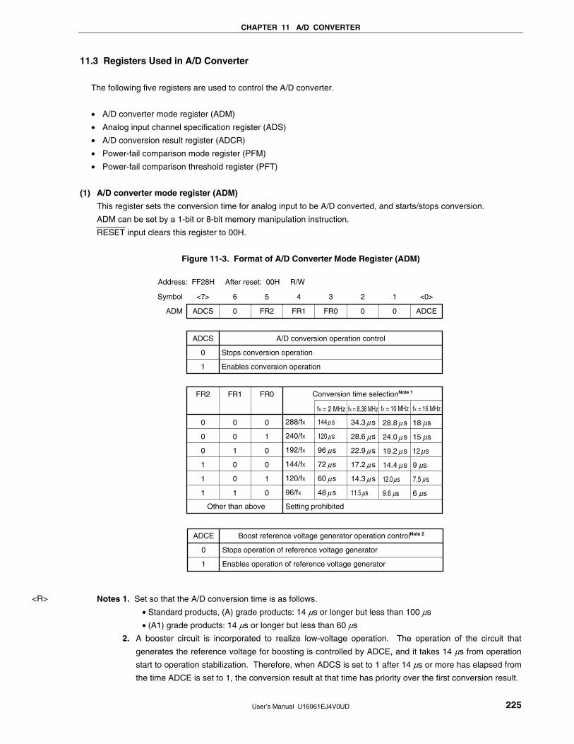
CHAPTER 11 A/D CONVERTER
User’s Manual U16961EJ4V0UD 225
11.3 Registers Used in A/D Converter
The following five registers are used to control the A/D converter.
• A/D converter mode register (ADM)
• Analog input channel specification register (ADS)
• A/D conversion result register (ADCR)
• Power-fail comparison mode register (PFM)
• Power-fail comparison threshold register (PFT)
(1) A/D converter mode register (ADM)
This register sets the conversion time for analog input to be A/D converted, and starts/stops conversion.
ADM can be set by a 1-bit or 8-bit memory manipulation instruction.
RESET input clears this register to 00H.
Figure 11-3. Format of A/D Converter Mode Register (ADM)
144 s
120 s
96 s
72 s
60 s
48 s
ADCE00FR0FR1FR20ADCS
A/D conversion operation control
Stops conversion operation
Enables conversion operation
ADCS
0
1
Conversion time selectionNote 1
288/fX
240/fX
192/fX
144/fX
120/fX
96/fX
Setting prohibited
FR2
0
0
0
1
1
1
Other than above
FR1
0
0
1
0
0
1
FR0
0
1
0
0
1
0
<0>123456<7>
ADM
Address: FF28H After reset: 00H R/W
Symbol
µ
µ
µ
µ
µ
µ
34.3 s
28.6 s
22.9 s
17.2 s
14.3 s
11.5 s
28.8 s
24.0 s
19.2 s
14.4 s
12.0 s
9.6 s
µ
µ
µ
µ
µ
µ
fX = 8.38 MHz fX = 10 MHz
18 s
15 s
12 s
9 s
7.5 s
6 s
µ
µ
µ
µ
µ
fX = 16 MHz
Boost reference voltage generator operation controlNote 2
Stops operation of reference voltage generator
Enables operation of reference voltage generator
ADCE
0
1
µ
µ
µ
µ
µ
µ
fX = 2 MHz
µ
Notes 1. Set so that the A/D conversion time is as follows.
• Standard products, (A) grade products: 14 µs or longer but less than 100 µs
• (A1) grade products: 14 µs or longer but less than 60 µs
2. A booster circuit is incorporated to realize low-voltage operation. The operation of the circuit that
generates the reference voltage for boosting is controlled by ADCE, and it takes 14 µs from operation
start to operation stabilization. Therefore, when ADCS is set to 1 after 14 µs or more has elapsed from
the time ADCE is set to 1, the conversion result at that time has priority over the first conversion result.
<R>
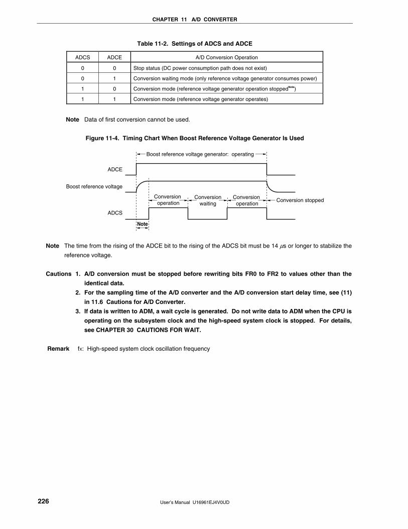
CHAPTER 11 A/D CONVERTER
User’s Manual U16961EJ4V0UD 226
Table 11-2. Settings of ADCS and ADCE
ADCS ADCE A/D Conversion Operation
0 0 Stop status (DC power consumption path does not exist)
0 1 Conversion waiting mode (only reference voltage generator consumes power)
1 0 Conversion mode (reference voltage generator operation stoppedNote)
1 1 Conversion mode (reference voltage generator operates)
Note Data of first conversion cannot be used.
Figure 11-4. Timing Chart When Boost Reference Voltage Generator Is Used
ADCE
Boost reference voltage
ADCS
Conversion operation
Conversion operation
Conversion stoppedConversionwaiting
Boost reference voltage generator: operating
Note
Note The time from the rising of the ADCE bit to the rising of the ADCS bit must be 14 µs or longer to stabilize the
reference voltage.
Cautions 1. A/D conversion must be stopped before rewriting bits FR0 to FR2 to values other than the
identical data.
2. For the sampling time of the A/D converter and the A/D conversion start delay time, see (11)
in 11.6 Cautions for A/D Converter.
3. If data is written to ADM, a wait cycle is generated. Do not write data to ADM when the CPU is
operating on the subsystem clock and the high-speed system clock is stopped. For details,
see CHAPTER 30 CAUTIONS FOR WAIT.
Remark fX: High-speed system clock oscillation frequency
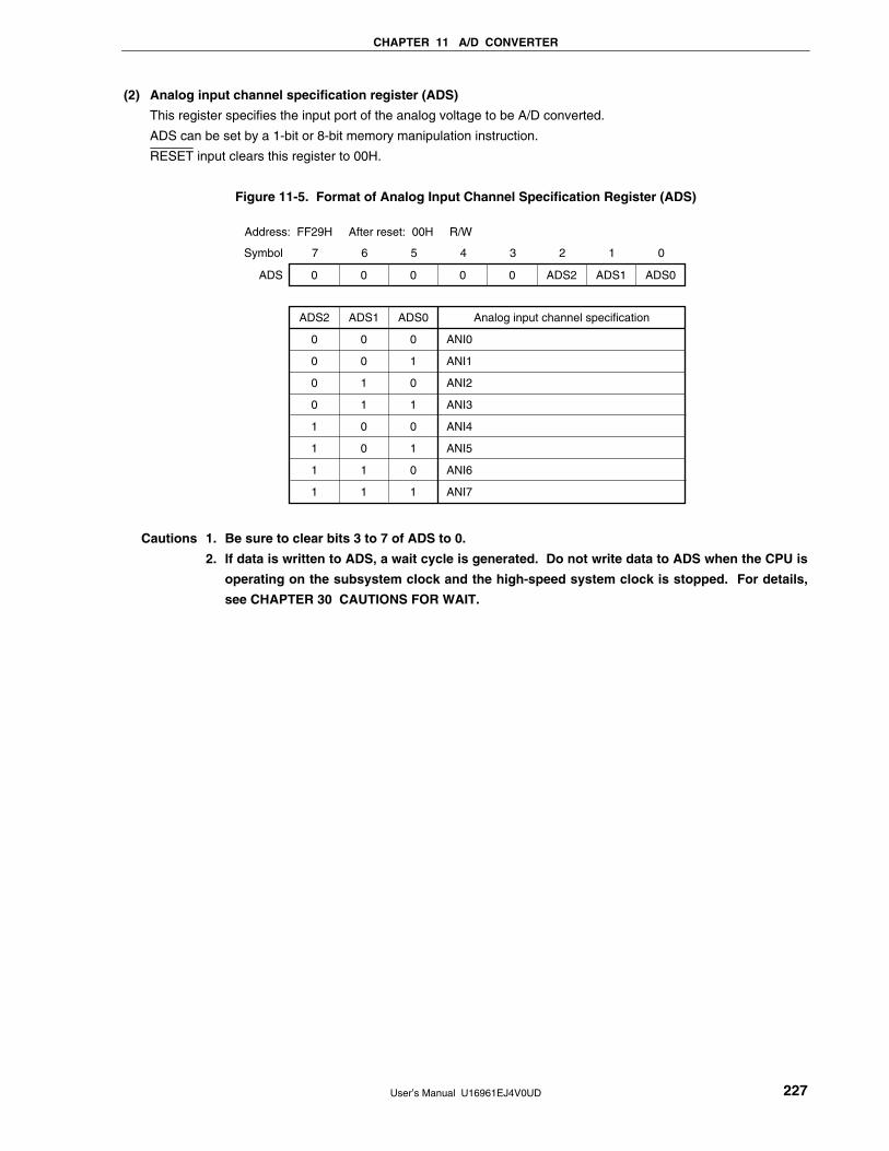
CHAPTER 11 A/D CONVERTER
User’s Manual U16961EJ4V0UD 227
(2) Analog input channel specification register (ADS)
This register specifies the input port of the analog voltage to be A/D converted.
ADS can be set by a 1-bit or 8-bit memory manipulation instruction.
RESET input clears this register to 00H.
Figure 11-5. Format of Analog Input Channel Specification Register (ADS)
ADS0ADS1ADS200000
Analog input channel specification
ANI0
ANI1
ANI2
ANI3
ANI4
ANI5
ANI6
ANI7
ADS0
0
1
0
1
0
1
0
1
ADS1
0
0
1
1
0
0
1
1
ADS2
0
0
0
0
1
1
1
1
01234567
ADS
Address: FF29H After reset: 00H R/W
Symbol
Cautions 1. Be sure to clear bits 3 to 7 of ADS to 0.
2. If data is written to ADS, a wait cycle is generated. Do not write data to ADS when the CPU is
operating on the subsystem clock and the high-speed system clock is stopped. For details,
see CHAPTER 30 CAUTIONS FOR WAIT.
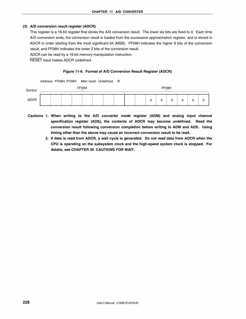
CHAPTER 11 A/D CONVERTER
User’s Manual U16961EJ4V0UD 228
(3) A/D conversion result register (ADCR)
This register is a 16-bit register that stores the A/D conversion result. The lower six bits are fixed to 0. Each time
A/D conversion ends, the conversion result is loaded from the successive approximation register, and is stored in
ADCR in order starting from the most significant bit (MSB). FF09H indicates the higher 8 bits of the conversion
result, and FF08H indicates the lower 2 bits of the conversion result.
ADCR can be read by a 16-bit memory manipulation instruction.
RESET input makes ADCR undefined.
Figure 11-6. Format of A/D Conversion Result Register (ADCR)
Symbol
Address: FF08H, FF09H After reset: Undefined R
FF09H FF08H
000000ADCR
Cautions 1. When writing to the A/D converter mode register (ADM) and analog input channel
specification register (ADS), the contents of ADCR may become undefined. Read the
conversion result following conversion completion before writing to ADM and ADS. Using
timing other than the above may cause an incorrect conversion result to be read.
2. If data is read from ADCR, a wait cycle is generated. Do not read data from ADCR when the
CPU is operating on the subsystem clock and the high-speed system clock is stopped. For
details, see CHAPTER 30 CAUTIONS FOR WAIT.
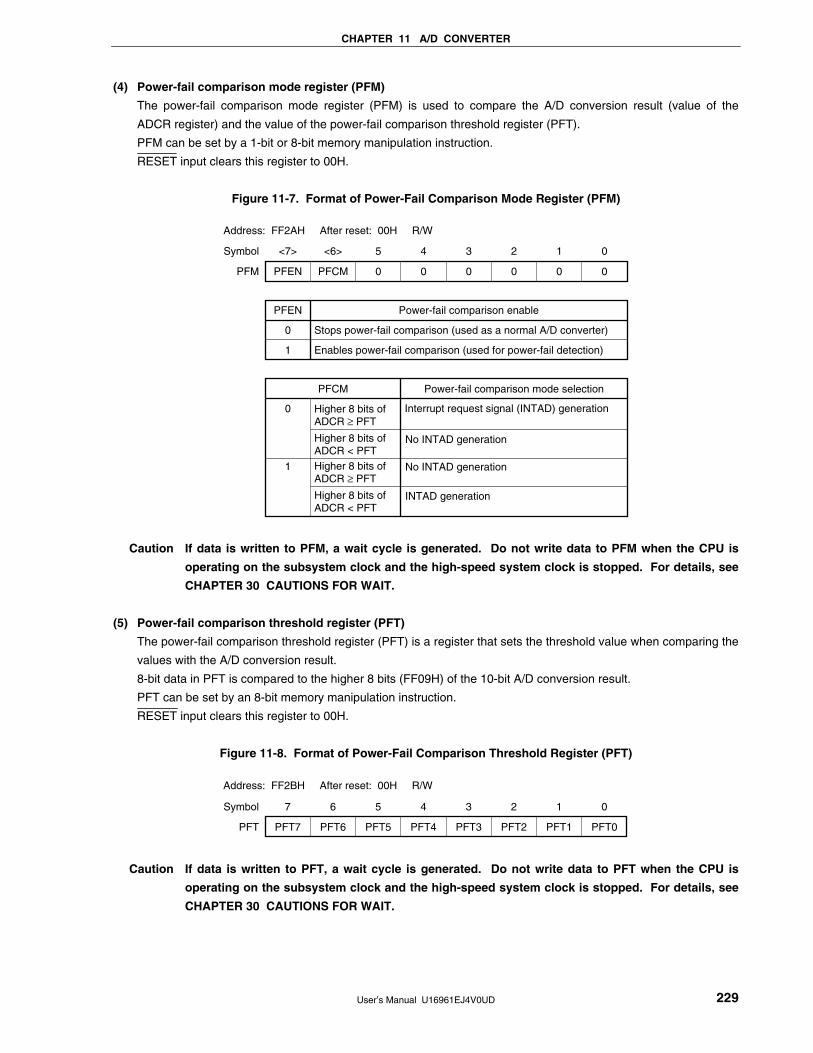
CHAPTER 11 A/D CONVERTER
User’s Manual U16961EJ4V0UD 229
(4) Power-fail comparison mode register (PFM)
The power-fail comparison mode register (PFM) is used to compare the A/D conversion result (value of the
ADCR register) and the value of the power-fail comparison threshold register (PFT).
PFM can be set by a 1-bit or 8-bit memory manipulation instruction.
RESET input clears this register to 00H.
Figure 11-7. Format of Power-Fail Comparison Mode Register (PFM)
000000PFCMPFEN
Power-fail comparison enable
Stops power-fail comparison (used as a normal A/D converter)
Enables power-fail comparison (used for power-fail detection)
PFEN
0
1
Power-fail comparison mode selection
Interrupt request signal (INTAD) generation
No INTAD generation
INTAD generation
No INTAD generation
Higher 8 bits ofADCR ≥ PFT
Higher 8 bits ofADCR < PFTHigher 8 bits ofADCR ≥ PFT
Higher 8 bits ofADCR < PFT
PFCM
0
1
012345<6><7>
PFM
Address: FF2AH After reset: 00H R/W
Symbol
Caution If data is written to PFM, a wait cycle is generated. Do not write data to PFM when the CPU is
operating on the subsystem clock and the high-speed system clock is stopped. For details, see
CHAPTER 30 CAUTIONS FOR WAIT.
(5) Power-fail comparison threshold register (PFT)
The power-fail comparison threshold register (PFT) is a register that sets the threshold value when comparing the
values with the A/D conversion result.
8-bit data in PFT is compared to the higher 8 bits (FF09H) of the 10-bit A/D conversion result.
PFT can be set by an 8-bit memory manipulation instruction.
RESET input clears this register to 00H.
Figure 11-8. Format of Power-Fail Comparison Threshold Register (PFT)
PFT0PFT1PFT2PFT3PFT4PFT5PFT6PFT7
01234567
PFT
Address: FF2BH After reset: 00H R/W
Symbol
Caution If data is written to PFT, a wait cycle is generated. Do not write data to PFT when the CPU is
operating on the subsystem clock and the high-speed system clock is stopped. For details, see
CHAPTER 30 CAUTIONS FOR WAIT.
CHAPTER 11 A/D CONVERTER
User’s Manual U16961EJ4V0UD 230
11.4 A/D Converter Operations
11.4.1 Basic operations of A/D converter
<1> Select one channel for A/D conversion using the analog input channel specification register (ADS).
<2> Set ADCE to 1 and wait for 14 µs or longer.
<3> Set ADCS to 1 and start the conversion operation.
(<4> to <10> are operations performed by hardware.)
<4> The voltage input to the selected analog input channel is sampled by the sample & hold circuit.
<5> When sampling has been done for a certain time, the sample & hold circuit is placed in the hold state and the
input analog voltage is held until the A/D conversion operation has ended.
<6> Bit 9 of the successive approximation register (SAR) is set. The series resistor string voltage tap is set to
(1/2) AVREF by the tap selector.
<7> The voltage difference between the series resistor string voltage tap and analog input is compared by the
voltage comparator. If the analog input is greater than (1/2) AVREF, the MSB of SAR remains set to 1. If the
analog input is smaller than (1/2) AVREF, the MSB is reset to 0.
<8> Next, bit 8 of SAR is automatically set to 1, and the operation proceeds to the next comparison. The series
resistor string voltage tap is selected according to the preset value of bit 9, as described below.
• Bit 9 = 1: (3/4) AVREF
• Bit 9 = 0: (1/4) AVREF
The voltage tap and analog input voltage are compared and bit 8 of SAR is manipulated as follows.
• Analog input voltage ≥ Voltage tap: Bit 8 = 1
• Analog input voltage < Voltage tap: Bit 8 = 0
<9> Comparison is continued in this way up to bit 0 of SAR.
<10> Upon completion of the comparison of 10 bits, an effective digital result value remains in SAR, and the result
value is transferred to the A/D conversion result register (ADCR) and then latched.
At the same time, the A/D conversion end interrupt request (INTAD) can also be generated.
<11> Repeat steps <4> to <10>, until ADCS is cleared to 0.
To stop the A/D converter, clear ADCS to 0.
To restart A/D conversion from the status of ADCE = 1, start from <3>. To restart A/D conversion from the
status of ADCE = 0, however, start from <2>.
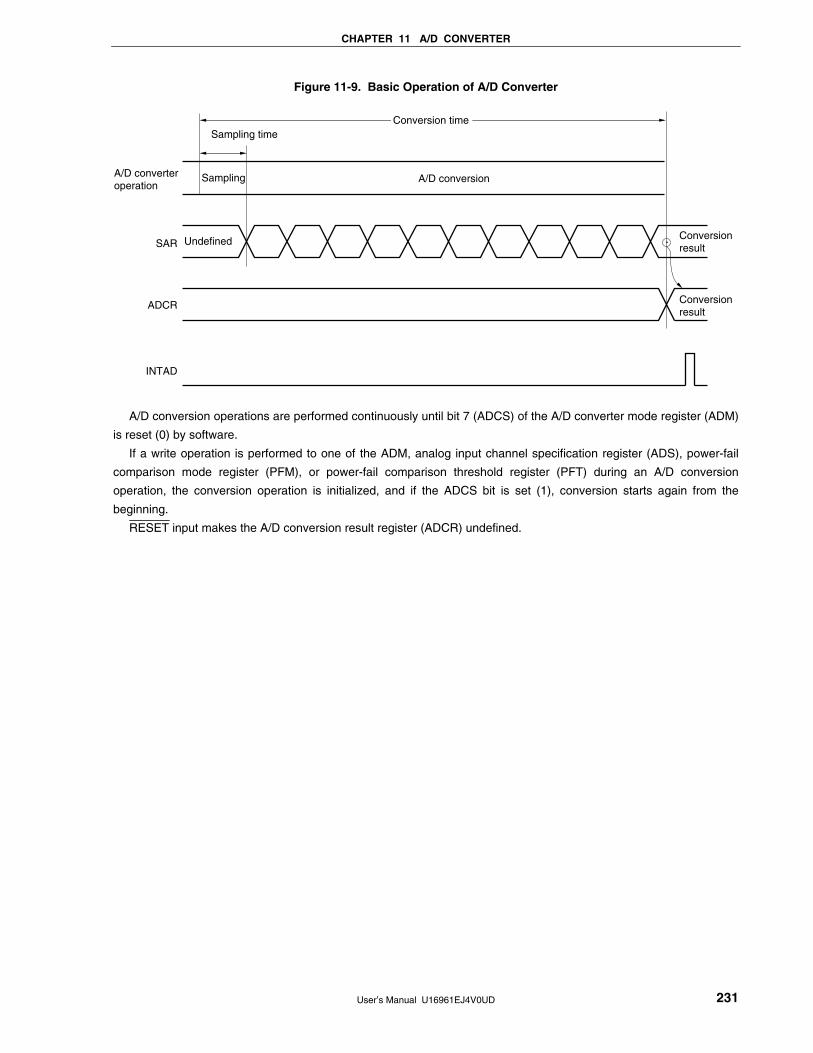
CHAPTER 11 A/D CONVERTER
User’s Manual U16961EJ4V0UD 231
Figure 11-9. Basic Operation of A/D Converter
Conversion time
Sampling time
Sampling A/D conversion
Undefined Conversion result
A/D converteroperation
SAR
ADCR
INTAD
Conversion result
A/D conversion operations are performed continuously until bit 7 (ADCS) of the A/D converter mode register (ADM)
is reset (0) by software.
If a write operation is performed to one of the ADM, analog input channel specification register (ADS), power-fail
comparison mode register (PFM), or power-fail comparison threshold register (PFT) during an A/D conversion
operation, the conversion operation is initialized, and if the ADCS bit is set (1), conversion starts again from the
beginning.
RESET input makes the A/D conversion result register (ADCR) undefined.
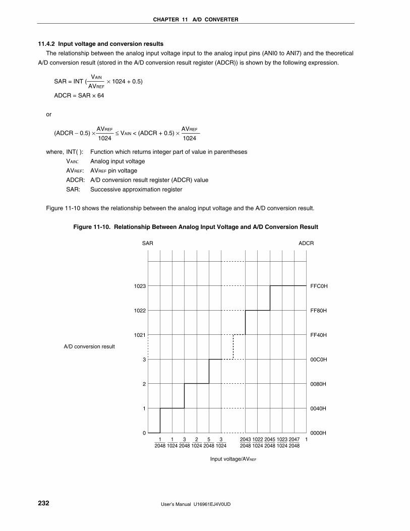
CHAPTER 11 A/D CONVERTER
User’s Manual U16961EJ4V0UD 232
11.4.2 Input voltage and conversion results
The relationship between the analog input voltage input to the analog input pins (ANI0 to ANI7) and the theoretical
A/D conversion result (stored in the A/D conversion result register (ADCR)) is shown by the following expression.
SAR = INT ( × 1024 + 0.5)
ADCR = SAR × 64
or
(ADCR − 0.5) × ≤ VAIN < (ADCR + 0.5) ×
where, INT( ): Function which returns integer part of value in parentheses
VAIN: Analog input voltage
AVREF: AVREF pin voltage
ADCR: A/D conversion result register (ADCR) value
SAR: Successive approximation register
Figure 11-10 shows the relationship between the analog input voltage and the A/D conversion result.
Figure 11-10. Relationship Between Analog Input Voltage and A/D Conversion Result
1023
1022
1021
3
2
1
0
FFC0H
FF80H
FF40H
00C0H
0080H
0040H
0000H
A/D conversion result
SAR ADCR
12048
11024
32048
21024
52048
Input voltage/AVREF
31024
20432048
10221024
20452048
10231024
20472048
1
VAIN
AVREF
AVREF
1024
AVREF
1024
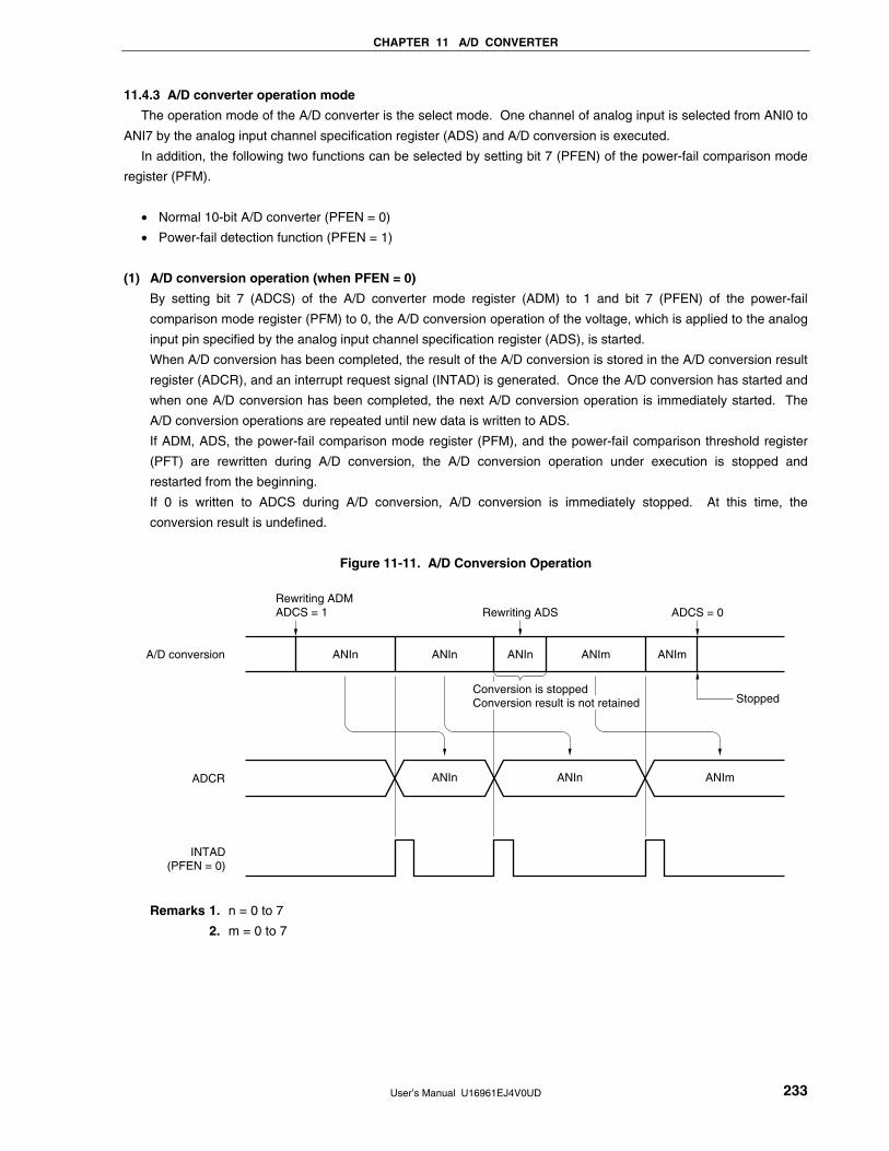
CHAPTER 11 A/D CONVERTER
User’s Manual U16961EJ4V0UD 233
11.4.3 A/D converter operation mode
The operation mode of the A/D converter is the select mode. One channel of analog input is selected from ANI0 to
ANI7 by the analog input channel specification register (ADS) and A/D conversion is executed.
In addition, the following two functions can be selected by setting bit 7 (PFEN) of the power-fail comparison mode
register (PFM).
• Normal 10-bit A/D converter (PFEN = 0)
• Power-fail detection function (PFEN = 1)
(1) A/D conversion operation (when PFEN = 0)
By setting bit 7 (ADCS) of the A/D converter mode register (ADM) to 1 and bit 7 (PFEN) of the power-fail
comparison mode register (PFM) to 0, the A/D conversion operation of the voltage, which is applied to the analog
input pin specified by the analog input channel specification register (ADS), is started.
When A/D conversion has been completed, the result of the A/D conversion is stored in the A/D conversion result
register (ADCR), and an interrupt request signal (INTAD) is generated. Once the A/D conversion has started and
when one A/D conversion has been completed, the next A/D conversion operation is immediately started. The
A/D conversion operations are repeated until new data is written to ADS.
If ADM, ADS, the power-fail comparison mode register (PFM), and the power-fail comparison threshold register
(PFT) are rewritten during A/D conversion, the A/D conversion operation under execution is stopped and
restarted from the beginning.
If 0 is written to ADCS during A/D conversion, A/D conversion is immediately stopped. At this time, the
conversion result is undefined.
Figure 11-11. A/D Conversion Operation
ANIn
Rewriting ADMADCS = 1 Rewriting ADS ADCS = 0
ANIn
ANIn ANIn ANIm
ANIn ANIm ANIm
Stopped
A/D conversion
ADCR
INTAD (PFEN = 0)
Conversion is stoppedConversion result is not retained
Remarks 1. n = 0 to 7
2. m = 0 to 7
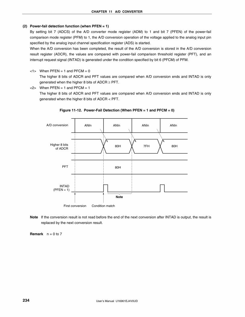
CHAPTER 11 A/D CONVERTER
User’s Manual U16961EJ4V0UD 234
(2) Power-fail detection function (when PFEN = 1)
By setting bit 7 (ADCS) of the A/D converter mode register (ADM) to 1 and bit 7 (PFEN) of the power-fail
comparison mode register (PFM) to 1, the A/D conversion operation of the voltage applied to the analog input pin
specified by the analog input channel specification register (ADS) is started.
When the A/D conversion has been completed, the result of the A/D conversion is stored in the A/D conversion
result register (ADCR), the values are compared with power-fail comparison threshold register (PFT), and an
interrupt request signal (INTAD) is generated under the condition specified by bit 6 (PFCM) of PFM.
<1> When PFEN = 1 and PFCM = 0
The higher 8 bits of ADCR and PFT values are compared when A/D conversion ends and INTAD is only
generated when the higher 8 bits of ADCR ≥ PFT.
<2> When PFEN = 1 and PFCM = 1
The higher 8 bits of ADCR and PFT values are compared when A/D conversion ends and INTAD is only
generated when the higher 8 bits of ADCR < PFT.
Figure 11-12. Power-Fail Detection (When PFEN = 1 and PFCM = 0)
A/D conversion
Higher 8 bitsof ADCR
PFT
INTAD(PFEN = 1)
ANIn ANIn
80H
80H
Condition matchFirst conversion
Note
7FH 80H
ANIn ANIn
Note If the conversion result is not read before the end of the next conversion after INTAD is output, the result is
replaced by the next conversion result.
Remark n = 0 to 7
CHAPTER 11 A/D CONVERTER
User’s Manual U16961EJ4V0UD 235
The setting methods are described below.
• When used as A/D conversion operation
<1> Set bit 0 (ADCE) of the A/D converter mode register (ADM) to 1.
<2> Select the channel and conversion time using bits 2 to 0 (ADS2 to ADS0) of the analog input channel
specification register (ADS) and bits 5 to 3 (FR2 to FR0) of ADM.
<3> Set bit 7 (ADCS) of ADM to 1 to start A/D conversion.
<4> An interrupt request signal (INTAD) is generated.
<5> Transfer the A/D conversion data to the A/D conversion result register (ADCR).
<Change the channel>
<6> Change the channel using bits 2 to 0 (ADS2 to ADS0) of ADS to start A/D conversion.
<7> An interrupt request signal (INTAD) is generated.
<8> Transfer the A/D conversion data to the A/D conversion result register (ADCR).
<Complete A/D conversion>
<9> Clear ADCS to 0.
<10> Clear ADCE to 0.
Cautions 1. Make sure the period of <1> to <3> is 14 µs or more.
2. It is no problem if the order of <1> and <2> is reversed.
3. <1> can be omitted. However, do not use the first conversion result after <3> in this
case.
4. The period from <4> to <7> differs from the conversion time set using bits 5 to 3 (FR2 to
FR0) of ADM. The period from <6> to <7> is the conversion time set using FR2 to FR0.
• When used as power-fail function
<1> Set bit 7 (PFEN) of the power-fail comparison mode register (PFM) to 1.
<2> Set power-fail comparison condition using bit 6 (PFCM) of PFM.
<3> Set bit 0 (ADCE) of the A/D converter mode register (ADM) to 1.
<4> Select the channel and conversion time using bits 2 to 0 (ADS2 to ADS0) of the analog input channel
specification register (ADS) and bits 5 to 3 (FR2 to FR0) of ADM.
<5> Set a threshold value to the power-fail comparison threshold register (PFT).
<6> Set bit 7 (ADCS) of ADM to 1.
<7> Transfer the A/D conversion data to the A/D conversion result register (ADCR).
<8> The higher 8 bits of ADCR and PFT are compared and an interrupt request signal (INTAD) is generated
if the conditions match.
<Change the channel>
<9> Change the channel using bits 2 to 0 (ADS2 to ADS0) of ADS.
<10> Transfer the A/D conversion data to the A/D conversion result register (ADCR).
<11> The higher 8 bits of ADCR and the power-fail comparison threshold register (PFT) are compared and an
interrupt request signal (INTAD) is generated if the conditions match.
<Complete A/D conversion>
<12> Clear ADCS to 0.
<13> Clear ADCE to 0.
Cautions 1. Make sure the period of <3> to <6> is 14 µs or more.
2. It is no problem if order of <3>, <4>, and <5> is changed.
3. <3> must not be omitted if the power-fail function is used.
4. The period from <7> to <11> differs from the conversion time set using bits 5 to 3 (FR2 to
FR0) of ADM. The period from <9> to <11> is the conversion time set using FR2 to FR0.
CHAPTER 11 A/D CONVERTER
User’s Manual U16961EJ4V0UD 236
11.5 How to Read A/D Converter Characteristics Table
Here, special terms unique to the A/D converter are explained.
(1) Resolution
This is the minimum analog input voltage that can be identified. That is, the percentage of the analog input
voltage per bit of digital output is called 1LSB (Least Significant Bit). The percentage of 1LSB with respect to the
full scale is expressed by %FSR (Full Scale Range).
1LSB is as follows when the resolution is 10 bits.
1LSB = 1/210 = 1/1024
= 0.098%FSR
Accuracy has no relation to resolution, but is determined by overall error.
(2) Overall error
This shows the maximum error value between the actual measured value and the theoretical value.
Zero-scale error, full-scale error, integral linearity error, and differential linearity errors that are combinations of
these express the overall error.
Note that the quantization error is not included in the overall error in the characteristics table.
(3) Quantization error
When analog values are converted to digital values, a ±1/2LSB error naturally occurs. In an A/D converter, an
analog input voltage in a range of ±1/2LSB is converted to the same digital code, so a quantization error cannot
be avoided.
Note that the quantization error is not included in the overall error, zero-scale error, full-scale error, integral
linearity error, and differential linearity error in the characteristics table.
Figure 11-13. Overall Error Figure 11-14. Quantization Error
Ideal line
0……0
1……1
Dig
ital o
utpu
t
Overallerror
Analog inputAVREF0
0……0
1……1
Dig
ital o
utpu
t
Quantization error1/2LSB
1/2LSB
Analog input0 AVREF
CHAPTER 11 A/D CONVERTER
User’s Manual U16961EJ4V0UD 237
(4) Zero-scale error
This shows the difference between the actual measurement value of the analog input voltage and the theoretical
value (1/2LSB) when the digital output changes from 0......000 to 0......001.
If the actual measurement value is greater than the theoretical value, it shows the difference between the actual
measurement value of the analog input voltage and the theoretical value (3/2LSB) when the digital output
changes from 0……001 to 0……010.
(5) Full-scale error
This shows the difference between the actual measurement value of the analog input voltage and the theoretical
value (Full-scale − 3/2LSB) when the digital output changes from 1......110 to 1......111.
(6) Integral linearity error
This shows the degree to which the conversion characteristics deviate from the ideal linear relationship. It
expresses the maximum value of the difference between the actual measurement value and the ideal straight line
when the zero-scale error and full-scale error are 0.
(7) Differential linearity error
While the ideal width of code output is 1LSB, this indicates the difference between the actual measurement value
and the ideal value.
Figure 11-15. Zero-Scale Error Figure 11-16. Full-Scale Error
111
011
010
001Zero-scale error
Ideal line
0000 1 2 3 AVREF
Dig
ital o
utpu
t (Lo
wer
3 b
its)
Analog input (LSB)
111
110
101
0000 AVREFAVREF–1AVREF–2AVREF–3
Dig
ital o
utpu
t (Lo
wer
3 b
its)
Analog input (LSB)
Ideal line
Full-scale error
Figure 11-17. Integral Linearity Error Figure 11-18. Differential Linearity Error
0 AVREF
Dig
ital o
utpu
t
Analog input
Integral linearityerror
Ideal line
1……1
0……0
0 AVREF
Dig
ital o
utpu
t
Analog input
Differential linearity error
1……1
0……0
Ideal 1LSB width
CHAPTER 11 A/D CONVERTER
User’s Manual U16961EJ4V0UD 238
(8) Conversion time
This expresses the time since sampling has been started until digital output is obtained.
The sampling time is included in the conversion time in the characteristics table.
(9) Sampling time
This is the time the analog switch is turned on for the analog voltage to be sampled by the sample & hold circuit.
Samplingtime
Conversion time
11.6 Cautions for A/D Converter
(1) Operating current in standby mode
The A/D converter stops operating in the standby mode. At this time, the operating current can be reduced by
clearing bit 7 (ADCS) and bit 0 (ADCE) of the A/D converter mode register (ADM) to 0 (see Figure 11-2).
(2) Input range of ANI0 to ANI7
Observe the rated range of the ANI0 to ANI7 input voltage. If a voltage of AVREF or higher and AVSS or lower
(even in the range of absolute maximum ratings) is input to an analog input channel, the converted value of that
channel becomes undefined. In addition, the converted values of the other channels may also be affected.
(3) Conflicting operations
<1> In case of conflict between A/D conversion result register (ADCR) write and ADCR read by instruction upon
the end of conversion,
ADCR read has priority. After the read operation, the new conversion result is written to ADCR.
<2> In case of conflict t between ADCR write and A/D converter mode register (ADM) write or analog input
channel specification register (ADS) write upon the end of conversion,
ADM or ADS write has priority. ADCR write is not performed, nor is the conversion end interrupt signal
(INTAD) generated.
<R>
CHAPTER 11 A/D CONVERTER
User’s Manual U16961EJ4V0UD 239
(4) Noise countermeasures
To maintain the 10-bit resolution, attention must be paid to noise input to the AVREF pin and pins ANI0 to ANI7.
Because the effect increases in proportion to the output impedance of the analog input source, it is recommended
that a capacitor be connected externally, as shown in Figure 11-19, to reduce noise.
Figure 11-19. Analog Input Pin Connection
Reference voltage
input
C = 100 to 1,000 pF
If there is a possibility that noise equal to or higher than AVREF or equal to or lower than AVSS may enter, clamp with a diode with a small VF value (0.3 V or lower).
AVREF
AVSS
VSS
ANI0 to ANI7
(5) ANI0/P20 to ANI7/P27
<1> The analog input pins (ANI0 to ANI7) are also used as input port pins (P20 to P27).
When A/D conversion is performed with any of ANI0 to ANI7 selected, do not access port 2 while
conversion is in progress; otherwise the conversion resolution may be degraded.
<2> If a digital pulse is applied to the pins adjacent to the pins currently used for A/D conversion, the expected
value of the A/D conversion may not be obtained due to coupling noise. Therefore, do not apply a pulse to
the pins adjacent to the pin undergoing A/D conversion.
(6) Input impedance of ANI0 to ANI7 pins
In this A/D converter, the internal sampling capacitor is charged and sampling is performed for approx. one sixth
of the conversion time.
Since only the leakage current flows other than during sampling and the current for charging the capacitor also
flows during sampling, the input impedance fluctuates and has no meaning.
To perform sufficient sampling, however, it is recommended to make the output impedance of the analog input
source 10 kΩ or lower, or attach a capacitor of around 100 pF to the ANI0 to ANI7 pins (see Figure 11-19).
(7) AVREF pin input impedance
A series resistor string of several tens of kΩ is connected between the AVREF and AVSS pins.
Therefore, if the output impedance of the reference voltage source is high, this will result in a series connection to
the series resistor string between the AVREF and AVSS pins, resulting in a large reference voltage error.
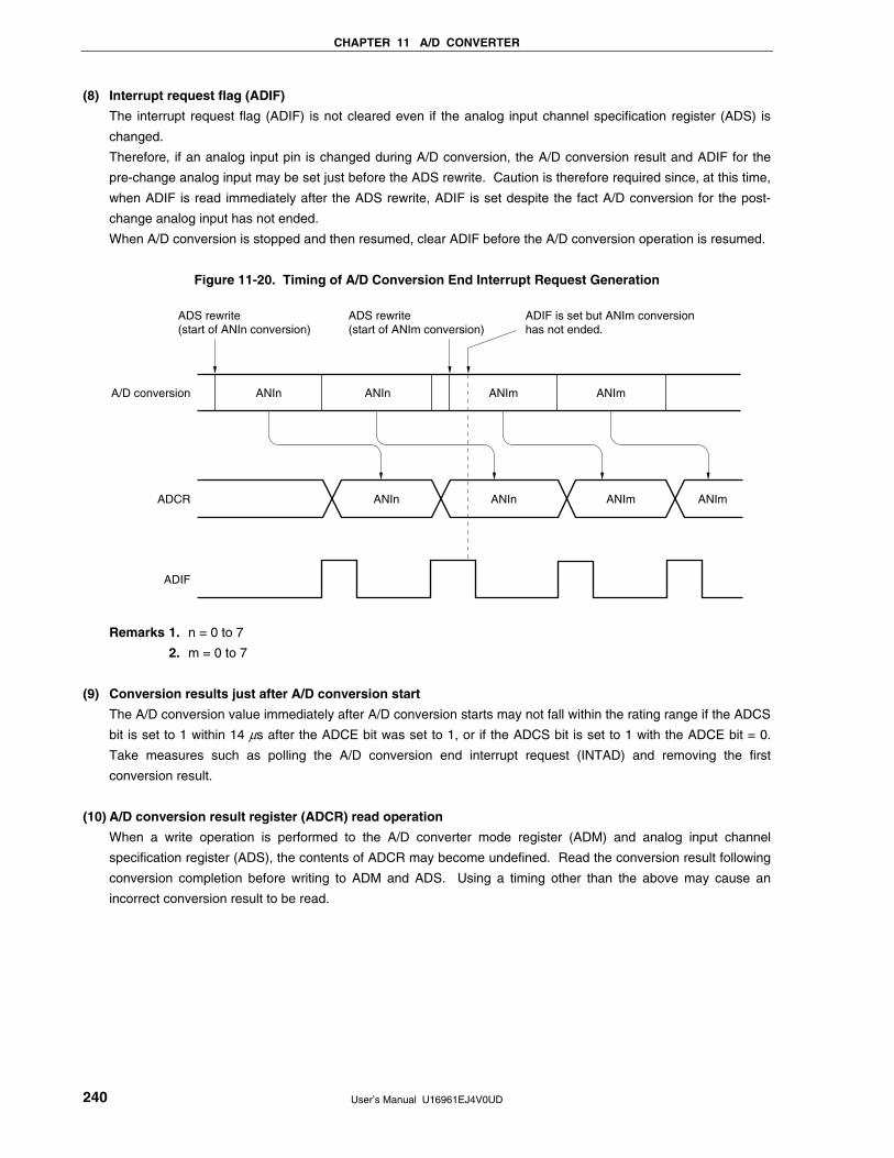
CHAPTER 11 A/D CONVERTER
User’s Manual U16961EJ4V0UD 240
(8) Interrupt request flag (ADIF)
The interrupt request flag (ADIF) is not cleared even if the analog input channel specification register (ADS) is
changed.
Therefore, if an analog input pin is changed during A/D conversion, the A/D conversion result and ADIF for the
pre-change analog input may be set just before the ADS rewrite. Caution is therefore required since, at this time,
when ADIF is read immediately after the ADS rewrite, ADIF is set despite the fact A/D conversion for the post-
change analog input has not ended.
When A/D conversion is stopped and then resumed, clear ADIF before the A/D conversion operation is resumed.
Figure 11-20. Timing of A/D Conversion End Interrupt Request Generation
ADS rewrite (start of ANIn conversion)
A/D conversion
ADCR
ADIF
ANIn ANIn ANIm ANIm
ANIn ANIn ANIm ANIm
ADS rewrite (start of ANIm conversion)
ADIF is set but ANIm conversion has not ended.
Remarks 1. n = 0 to 7
2. m = 0 to 7
(9) Conversion results just after A/D conversion start
The A/D conversion value immediately after A/D conversion starts may not fall within the rating range if the ADCS
bit is set to 1 within 14 µs after the ADCE bit was set to 1, or if the ADCS bit is set to 1 with the ADCE bit = 0.
Take measures such as polling the A/D conversion end interrupt request (INTAD) and removing the first
conversion result.
(10) A/D conversion result register (ADCR) read operation
When a write operation is performed to the A/D converter mode register (ADM) and analog input channel
specification register (ADS), the contents of ADCR may become undefined. Read the conversion result following
conversion completion before writing to ADM and ADS. Using a timing other than the above may cause an
incorrect conversion result to be read.
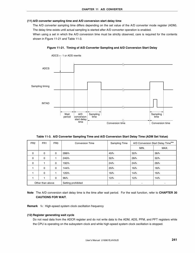
CHAPTER 11 A/D CONVERTER
User’s Manual U16961EJ4V0UD 241
(11) A/D converter sampling time and A/D conversion start delay time
The A/D converter sampling time differs depending on the set value of the A/D converter mode register (ADM).
The delay time exists until actual sampling is started after A/D converter operation is enabled.
When using a set in which the A/D conversion time must be strictly observed, care is required for the contents
shown in Figure 11-21 and Table 11-3.
Figure 11-21. Timing of A/D Converter Sampling and A/D Conversion Start Delay
ADCS
Waitperiod
Conversion time Conversion time
A/D conversion start delay
time
Samplingtime
Sampling timing
INTAD
ADCS ← 1 or ADS rewrite
Samplingtime
Table 11-3. A/D Converter Sampling Time and A/D Conversion Start Delay Time (ADM Set Value)
A/D Conversion Start Delay TimeNote FR2 FR1 FR0 Conversion Time Sampling Time
MIN. MAX.
0 0 0 288/fX 40/fX 32/fX 36/fX
0 0 1 240/fX 32/fX 28/fX 32/fX
0 1 0 192/fX 24/fX 24/fX 28/fX
1 0 0 144/fX 20/fX 16/fX 18/fX
1 0 1 120/fX 16/fX 14/fX 16/fX
1 1 0 96/fX 12/fX 12/fX 14/fX
Other than above Setting prohibited − − −
Note The A/D conversion start delay time is the time after wait period. For the wait function, refer to CHAPTER 30
CAUTIONS FOR WAIT.
Remark fX: High-speed system clock oscillation frequency
(12) Register generating wait cycle
Do not read data from the ADCR register and do not write data to the ADM, ADS, PFM, and PFT registers while
the CPU is operating on the subsystem clock and while high-speed system clock oscillation is stopped.
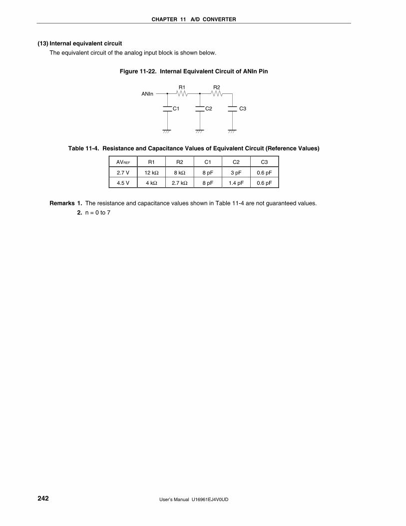
CHAPTER 11 A/D CONVERTER
User’s Manual U16961EJ4V0UD 242
(13) Internal equivalent circuit
The equivalent circuit of the analog input block is shown below.
Figure 11-22. Internal Equivalent Circuit of ANIn Pin
ANIn
C1 C2 C3
R1 R2
Table 11-4. Resistance and Capacitance Values of Equivalent Circuit (Reference Values)
AVREF R1 R2 C1 C2 C3
2.7 V 12 kΩ 8 kΩ 8 pF 3 pF 0.6 pF
4.5 V 4 kΩ 2.7 kΩ 8 pF 1.4 pF 0.6 pF
Remarks 1. The resistance and capacitance values shown in Table 11-4 are not guaranteed values.
2. n = 0 to 7
User’s Manual U16961EJ4V0UD 243
CHAPTER 12 SERIAL INTERFACE UART0
12.1 Functions of Serial Interface UART0
Serial interface UART0 has the following two modes.
(1) Operation stop mode
This mode is used when serial communication is not executed and can enable a reduction in the power
consumption.
For details, see 12.4.1 Operation stop mode.
(2) Asynchronous serial interface (UART) mode
The functions of this mode are outlined below.
For details, see 12.4.2 Asynchronous serial interface (UART) mode and 12.4.3 Dedicated baud rate
generator.
• Two-pin configuration TXD0: Transmit data output pin
RXD0: Receive data input pin
• Length of communication data can be selected from 7 or 8 bits.
• Dedicated on-chip 5-bit baud rate generator allowing any baud rate to be set
• Transmission and reception can be performed independently.
• Four operating clock inputs selectable
• Fixed to LSB-first communication
Cautions 1. If clock supply to serial interface UART0 is not stopped (e.g., in the HALT mode), normal
operation continues. If clock supply to serial interface UART0 is stopped (e.g., in the STOP
mode), each register stops operating, and holds the value immediately before clock supply
was stopped. The TXD0 pin also holds the value immediately before clock supply was
stopped and outputs it. However, the operation is not guaranteed after clock supply is
resumed. Therefore, reset the circuit so that POWER0 = 0, RXE0 = 0, and TXE0 = 0.
2. Set POWER0 = 1 and then set TXE0 = 1 (transmission) or RXE0 = 1 (reception) to start
communication.
3. TXE0 and RXE0 are synchronized by the base clock (fXCLK0) set by BRGC0. To enable
transmission or reception again, set TXE0 or RXE0 to 1 at least two clocks of base clock
after TXE0 or RXE0 has been cleared to 0. If TXE0 or RXE0 is set within two clocks of base
clock, the transmission circuit or reception circuit may not be initialized.
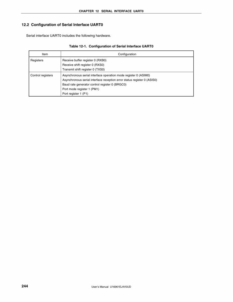
CHAPTER 12 SERIAL INTERFACE UART0
User’s Manual U16961EJ4V0UD 244
12.2 Configuration of Serial Interface UART0
Serial interface UART0 includes the following hardware.
Table 12-1. Configuration of Serial Interface UART0
Item Configuration
Registers Receive buffer register 0 (RXB0)
Receive shift register 0 (RXS0)
Transmit shift register 0 (TXS0)
Control registers Asynchronous serial interface operation mode register 0 (ASIM0)
Asynchronous serial interface reception error status register 0 (ASIS0)
Baud rate generator control register 0 (BRGC0)
Port mode register 1 (PM1)
Port register 1 (P1)
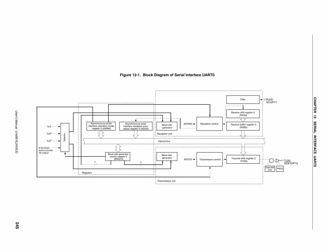
CH
AP
TE
R 12 S
ER
IAL
INT
ER
FA
CE
UA
RT
0
User’s M
anual U16961E
J4V0U
D
245
Figure 12-1. Block Diagram of Serial Interface UART0
TxD0/SCK10/P10
INTST0
RxD0/SI10/P11
INTSR0
fX/25
fX/23
fX/2
Transmit shift register 0 (TXS0)
Receive shift register 0 (RXS0)
Receive buffer register 0(RXB0)
Asynchronous serial interface reception error status register 0 (ASIS0)
Asynchronous serial interface operation mode
register 0 (ASIM0)
Baud rate generator control register 0
(BRGC0)
8-bit timer/event counter50 output
Registers
Sel
ecto
r
Baud rate generator
Baud rate generator
Reception unit
Reception control
Filter
Internal bus
Transmission control
Transmission unit
Output latch(P10)
PM10
7 7
CHAPTER 12 SERIAL INTERFACE UART0
User’s Manual U16961EJ4V0UD 246
(1) Receive buffer register 0 (RXB0)
This 8-bit register stores parallel data converted by receive shift register 0 (RXS0).
Each time 1 byte of data has been received, new receive data is transferred to this register from receive shift
register 0 (RXS0).
If the data length is set to 7 bits, the receive data is transferred to bits 0 to 6 of RXB0 and the MSB of RXB0 is
always 0.
If an overrun error (OVE0) occurs, the receive data is not transferred to RXB0.
RXB0 can be read by an 8-bit memory manipulation instruction. No data can be written to this register.
RESET input or POWER0 = 0 sets this register to FFH.
(2) Receive shift register 0 (RXS0)
This register converts the serial data input to the RXD0 pin into parallel data.
RXS0 cannot be directly manipulated by a program.
(3) Transmit shift register 0 (TXS0)
This register is used to set transmit data. Transmission is started when data is written to TXS0, and serial data is
transmitted from the TXD0 pins.
TXS0 can be written by an 8-bit memory manipulation instruction. This register cannot be read.
RESET input, POWER0 = 0, or TXE0 = 0 sets this register to FFH.
Caution Do not write the next transmit data to TXS0 before the transmission completion interrupt signal
(INTST0) is generated.
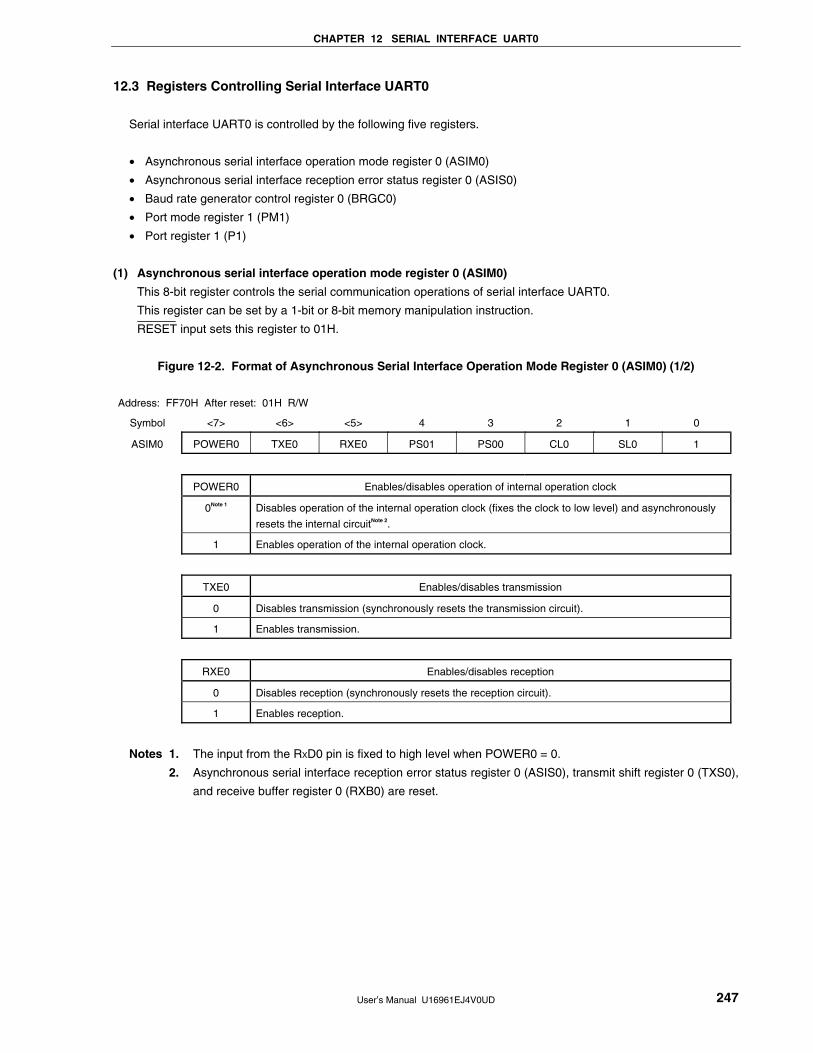
CHAPTER 12 SERIAL INTERFACE UART0
User’s Manual U16961EJ4V0UD 247
12.3 Registers Controlling Serial Interface UART0
Serial interface UART0 is controlled by the following five registers.
• Asynchronous serial interface operation mode register 0 (ASIM0)
• Asynchronous serial interface reception error status register 0 (ASIS0)
• Baud rate generator control register 0 (BRGC0)
• Port mode register 1 (PM1)
• Port register 1 (P1)
(1) Asynchronous serial interface operation mode register 0 (ASIM0)
This 8-bit register controls the serial communication operations of serial interface UART0.
This register can be set by a 1-bit or 8-bit memory manipulation instruction.
RESET input sets this register to 01H.
Figure 12-2. Format of Asynchronous Serial Interface Operation Mode Register 0 (ASIM0) (1/2)
Address: FF70H After reset: 01H R/W
Symbol <7> <6> <5> 4 3 2 1 0
ASIM0 POWER0 TXE0 RXE0 PS01 PS00 CL0 SL0 1
POWER0 Enables/disables operation of internal operation clock
0Note 1 Disables operation of the internal operation clock (fixes the clock to low level) and asynchronously
resets the internal circuitNote 2.
1 Enables operation of the internal operation clock.
TXE0 Enables/disables transmission
0 Disables transmission (synchronously resets the transmission circuit).
1 Enables transmission.
RXE0 Enables/disables reception
0 Disables reception (synchronously resets the reception circuit).
1 Enables reception.
Notes 1. The input from the RXD0 pin is fixed to high level when POWER0 = 0.
2. Asynchronous serial interface reception error status register 0 (ASIS0), transmit shift register 0 (TXS0),
and receive buffer register 0 (RXB0) are reset.
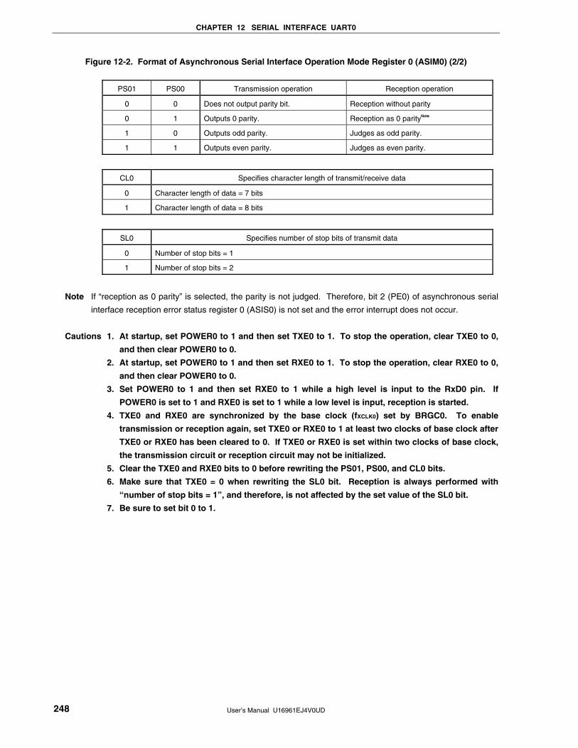
CHAPTER 12 SERIAL INTERFACE UART0
User’s Manual U16961EJ4V0UD 248
Figure 12-2. Format of Asynchronous Serial Interface Operation Mode Register 0 (ASIM0) (2/2)
PS01 PS00 Transmission operation Reception operation
0 0 Does not output parity bit. Reception without parity
0 1 Outputs 0 parity. Reception as 0 parityNote
1 0 Outputs odd parity. Judges as odd parity.
1 1 Outputs even parity. Judges as even parity.
CL0 Specifies character length of transmit/receive data
0 Character length of data = 7 bits
1 Character length of data = 8 bits
SL0 Specifies number of stop bits of transmit data
0 Number of stop bits = 1
1 Number of stop bits = 2
Note If “reception as 0 parity” is selected, the parity is not judged. Therefore, bit 2 (PE0) of asynchronous serial
interface reception error status register 0 (ASIS0) is not set and the error interrupt does not occur.
Cautions 1. At startup, set POWER0 to 1 and then set TXE0 to 1. To stop the operation, clear TXE0 to 0,
and then clear POWER0 to 0.
2. At startup, set POWER0 to 1 and then set RXE0 to 1. To stop the operation, clear RXE0 to 0,
and then clear POWER0 to 0.
3. Set POWER0 to 1 and then set RXE0 to 1 while a high level is input to the RxD0 pin. If
POWER0 is set to 1 and RXE0 is set to 1 while a low level is input, reception is started.
4. TXE0 and RXE0 are synchronized by the base clock (fXCLK0) set by BRGC0. To enable
transmission or reception again, set TXE0 or RXE0 to 1 at least two clocks of base clock after
TXE0 or RXE0 has been cleared to 0. If TXE0 or RXE0 is set within two clocks of base clock,
the transmission circuit or reception circuit may not be initialized.
5. Clear the TXE0 and RXE0 bits to 0 before rewriting the PS01, PS00, and CL0 bits.
6. Make sure that TXE0 = 0 when rewriting the SL0 bit. Reception is always performed with
“number of stop bits = 1”, and therefore, is not affected by the set value of the SL0 bit.
7. Be sure to set bit 0 to 1.
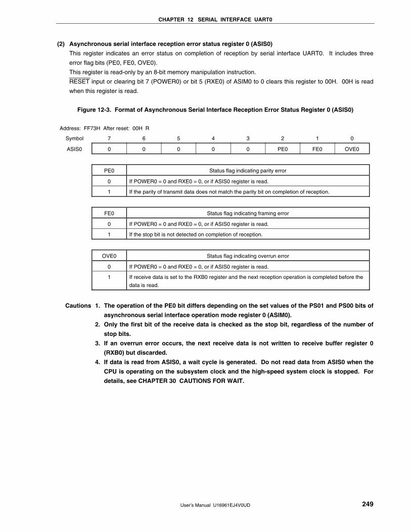
CHAPTER 12 SERIAL INTERFACE UART0
User’s Manual U16961EJ4V0UD 249
(2) Asynchronous serial interface reception error status register 0 (ASIS0)
This register indicates an error status on completion of reception by serial interface UART0. It includes three
error flag bits (PE0, FE0, OVE0).
This register is read-only by an 8-bit memory manipulation instruction.
RESET input or clearing bit 7 (POWER0) or bit 5 (RXE0) of ASIM0 to 0 clears this register to 00H. 00H is read
when this register is read.
Figure 12-3. Format of Asynchronous Serial Interface Reception Error Status Register 0 (ASIS0)
Address: FF73H After reset: 00H R
Symbol 7 6 5 4 3 2 1 0
ASIS0 0 0 0 0 0 PE0 FE0 OVE0
PE0 Status flag indicating parity error
0 If POWER0 = 0 and RXE0 = 0, or if ASIS0 register is read.
1 If the parity of transmit data does not match the parity bit on completion of reception.
FE0 Status flag indicating framing error
0 If POWER0 = 0 and RXE0 = 0, or if ASIS0 register is read.
1 If the stop bit is not detected on completion of reception.
OVE0 Status flag indicating overrun error
0 If POWER0 = 0 and RXE0 = 0, or if ASIS0 register is read.
1 If receive data is set to the RXB0 register and the next reception operation is completed before the
data is read.
Cautions 1. The operation of the PE0 bit differs depending on the set values of the PS01 and PS00 bits of
asynchronous serial interface operation mode register 0 (ASIM0).
2. Only the first bit of the receive data is checked as the stop bit, regardless of the number of
stop bits.
3. If an overrun error occurs, the next receive data is not written to receive buffer register 0
(RXB0) but discarded.
4. If data is read from ASIS0, a wait cycle is generated. Do not read data from ASIS0 when the
CPU is operating on the subsystem clock and the high-speed system clock is stopped. For
details, see CHAPTER 30 CAUTIONS FOR WAIT.
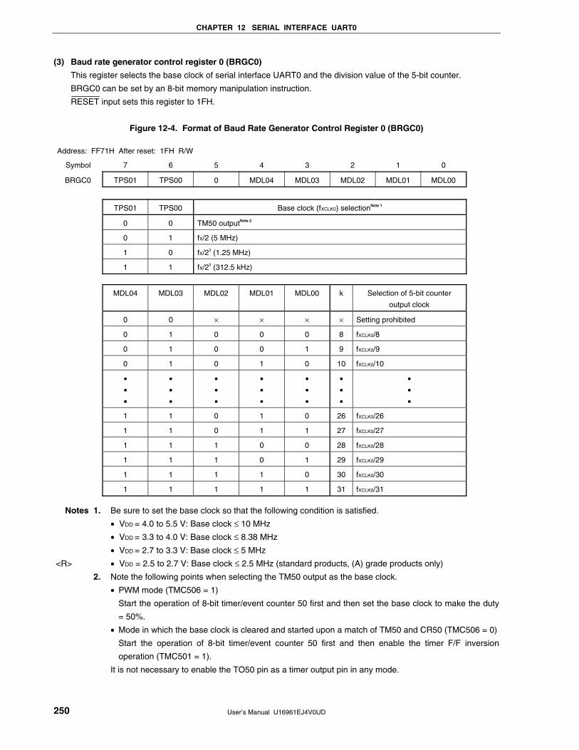
CHAPTER 12 SERIAL INTERFACE UART0
User’s Manual U16961EJ4V0UD 250
(3) Baud rate generator control register 0 (BRGC0)
This register selects the base clock of serial interface UART0 and the division value of the 5-bit counter.
BRGC0 can be set by an 8-bit memory manipulation instruction.
RESET input sets this register to 1FH.
Figure 12-4. Format of Baud Rate Generator Control Register 0 (BRGC0)
Address: FF71H After reset: 1FH R/W
Symbol 7 6 5 4 3 2 1 0
BRGC0 TPS01 TPS00 0 MDL04 MDL03 MDL02 MDL01 MDL00
TPS01 TPS00 Base clock (fXCLK0) selectionNote 1
0 0 TM50 outputNote 2
0 1 fX/2 (5 MHz)
1 0 fX/23 (1.25 MHz)
1 1 fX/25 (312.5 kHz)
MDL04 MDL03 MDL02 MDL01 MDL00 k Selection of 5-bit counter
output clock
0 0 × × × × Setting prohibited
0 1 0 0 0 8 fXCLK0/8
0 1 0 0 1 9 fXCLK0/9
0 1 0 1 0 10 fXCLK0/10
•
•
•
•
•
•
•
•
•
•
•
•
•
•
•
•
•
•
•
•
•
1 1 0 1 0 26 fXCLK0/26
1 1 0 1 1 27 fXCLK0/27
1 1 1 0 0 28 fXCLK0/28
1 1 1 0 1 29 fXCLK0/29
1 1 1 1 0 30 fXCLK0/30
1 1 1 1 1 31 fXCLK0/31
Notes 1. Be sure to set the base clock so that the following condition is satisfied.
• VDD = 4.0 to 5.5 V: Base clock ≤ 10 MHz
• VDD = 3.3 to 4.0 V: Base clock ≤ 8.38 MHz
• VDD = 2.7 to 3.3 V: Base clock ≤ 5 MHz
• VDD = 2.5 to 2.7 V: Base clock ≤ 2.5 MHz (standard products, (A) grade products only)
2. Note the following points when selecting the TM50 output as the base clock.
• PWM mode (TMC506 = 1)
Start the operation of 8-bit timer/event counter 50 first and then set the base clock to make the duty
= 50%.
• Mode in which the base clock is cleared and started upon a match of TM50 and CR50 (TMC506 = 0)
Start the operation of 8-bit timer/event counter 50 first and then enable the timer F/F inversion
operation (TMC501 = 1).
It is not necessary to enable the TO50 pin as a timer output pin in any mode.
<R>
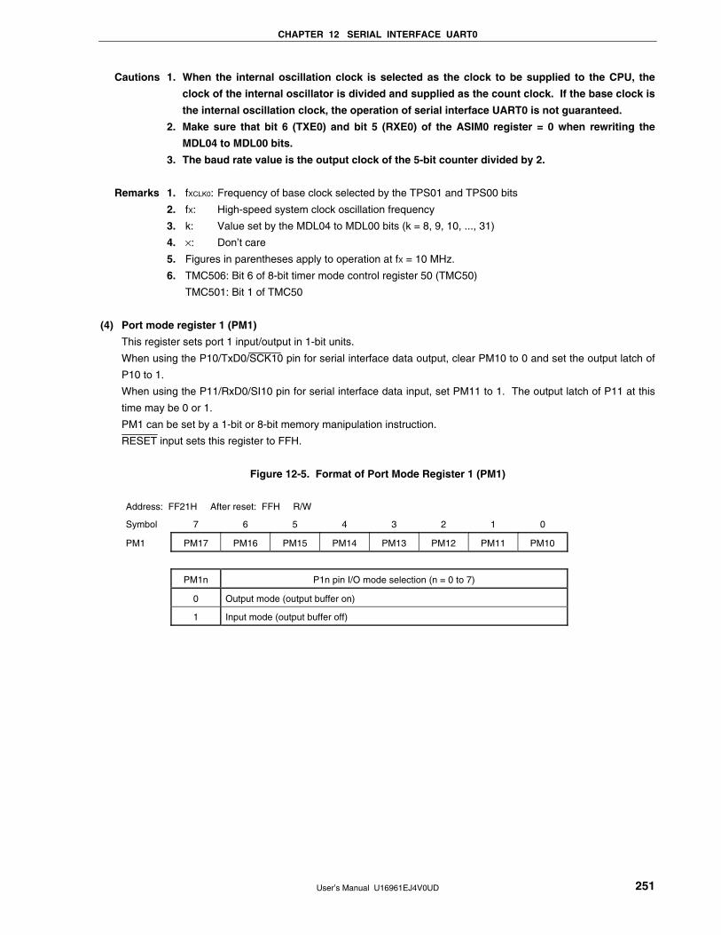
CHAPTER 12 SERIAL INTERFACE UART0
User’s Manual U16961EJ4V0UD 251
Cautions 1. When the internal oscillation clock is selected as the clock to be supplied to the CPU, the
clock of the internal oscillator is divided and supplied as the count clock. If the base clock is
the internal oscillation clock, the operation of serial interface UART0 is not guaranteed.
2. Make sure that bit 6 (TXE0) and bit 5 (RXE0) of the ASIM0 register = 0 when rewriting the
MDL04 to MDL00 bits.
3. The baud rate value is the output clock of the 5-bit counter divided by 2.
Remarks 1. fXCLK0: Frequency of base clock selected by the TPS01 and TPS00 bits
2. fX: High-speed system clock oscillation frequency
3. k: Value set by the MDL04 to MDL00 bits (k = 8, 9, 10, ..., 31)
4. ×: Don’t care
5. Figures in parentheses apply to operation at fX = 10 MHz.
6. TMC506: Bit 6 of 8-bit timer mode control register 50 (TMC50)
TMC501: Bit 1 of TMC50
(4) Port mode register 1 (PM1)
This register sets port 1 input/output in 1-bit units.
When using the P10/TxD0/SCK10 pin for serial interface data output, clear PM10 to 0 and set the output latch of
P10 to 1.
When using the P11/RxD0/SI10 pin for serial interface data input, set PM11 to 1. The output latch of P11 at this
time may be 0 or 1.
PM1 can be set by a 1-bit or 8-bit memory manipulation instruction.
RESET input sets this register to FFH.
Figure 12-5. Format of Port Mode Register 1 (PM1)
Address: FF21H After reset: FFH R/W
Symbol 7 6 5 4 3 2 1 0
PM1 PM17 PM16 PM15 PM14 PM13 PM12 PM11 PM10
PM1n P1n pin I/O mode selection (n = 0 to 7)
0 Output mode (output buffer on)
1 Input mode (output buffer off)
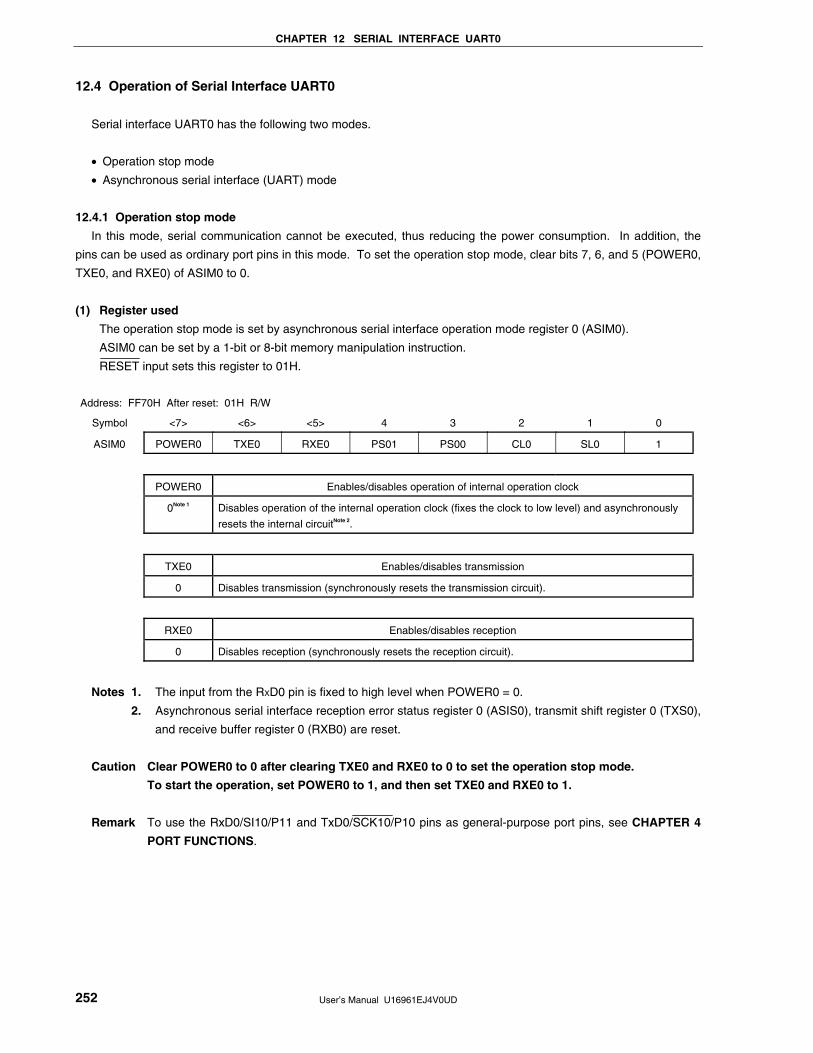
CHAPTER 12 SERIAL INTERFACE UART0
User’s Manual U16961EJ4V0UD 252
12.4 Operation of Serial Interface UART0
Serial interface UART0 has the following two modes.
• Operation stop mode
• Asynchronous serial interface (UART) mode
12.4.1 Operation stop mode
In this mode, serial communication cannot be executed, thus reducing the power consumption. In addition, the
pins can be used as ordinary port pins in this mode. To set the operation stop mode, clear bits 7, 6, and 5 (POWER0,
TXE0, and RXE0) of ASIM0 to 0.
(1) Register used
The operation stop mode is set by asynchronous serial interface operation mode register 0 (ASIM0).
ASIM0 can be set by a 1-bit or 8-bit memory manipulation instruction.
RESET input sets this register to 01H.
Address: FF70H After reset: 01H R/W
Symbol <7> <6> <5> 4 3 2 1 0
ASIM0 POWER0 TXE0 RXE0 PS01 PS00 CL0 SL0 1
POWER0 Enables/disables operation of internal operation clock
0Note 1 Disables operation of the internal operation clock (fixes the clock to low level) and asynchronously
resets the internal circuitNote 2.
TXE0 Enables/disables transmission
0 Disables transmission (synchronously resets the transmission circuit).
RXE0 Enables/disables reception
0 Disables reception (synchronously resets the reception circuit).
Notes 1. The input from the RXD0 pin is fixed to high level when POWER0 = 0.
2. Asynchronous serial interface reception error status register 0 (ASIS0), transmit shift register 0 (TXS0),
and receive buffer register 0 (RXB0) are reset.
Caution Clear POWER0 to 0 after clearing TXE0 and RXE0 to 0 to set the operation stop mode.
To start the operation, set POWER0 to 1, and then set TXE0 and RXE0 to 1.
Remark To use the RxD0/SI10/P11 and TxD0/SCK10/P10 pins as general-purpose port pins, see CHAPTER 4
PORT FUNCTIONS.
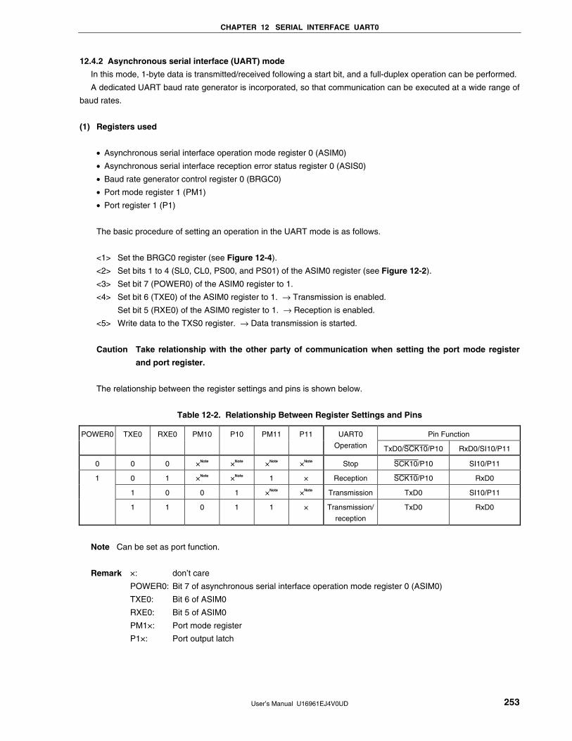
CHAPTER 12 SERIAL INTERFACE UART0
User’s Manual U16961EJ4V0UD 253
12.4.2 Asynchronous serial interface (UART) mode
In this mode, 1-byte data is transmitted/received following a start bit, and a full-duplex operation can be performed.
A dedicated UART baud rate generator is incorporated, so that communication can be executed at a wide range of
baud rates.
(1) Registers used
• Asynchronous serial interface operation mode register 0 (ASIM0)
• Asynchronous serial interface reception error status register 0 (ASIS0)
• Baud rate generator control register 0 (BRGC0)
• Port mode register 1 (PM1)
• Port register 1 (P1)
The basic procedure of setting an operation in the UART mode is as follows.
<1> Set the BRGC0 register (see Figure 12-4).
<2> Set bits 1 to 4 (SL0, CL0, PS00, and PS01) of the ASIM0 register (see Figure 12-2).
<3> Set bit 7 (POWER0) of the ASIM0 register to 1.
<4> Set bit 6 (TXE0) of the ASIM0 register to 1. → Transmission is enabled.
Set bit 5 (RXE0) of the ASIM0 register to 1. → Reception is enabled.
<5> Write data to the TXS0 register. → Data transmission is started.
Caution Take relationship with the other party of communication when setting the port mode register
and port register.
The relationship between the register settings and pins is shown below.
Table 12-2. Relationship Between Register Settings and Pins
Pin Function POWER0 TXE0 RXE0 PM10 P10 PM11 P11 UART0
Operation TxD0/SCK10/P10 RxD0/SI10/P11
0 0 0 ×Note ×Note ×Note ×Note Stop SCK10/P10 SI10/P11
0 1 ×Note ×Note 1 × Reception SCK10/P10 RxD0
1 0 0 1 ×Note ×Note Transmission TxD0 SI10/P11
1
1 1 0 1 1 × Transmission/
reception
TxD0 RxD0
Note Can be set as port function.
Remark ×: don’t care
POWER0: Bit 7 of asynchronous serial interface operation mode register 0 (ASIM0)
TXE0: Bit 6 of ASIM0
RXE0: Bit 5 of ASIM0
PM1×: Port mode register
P1×: Port output latch
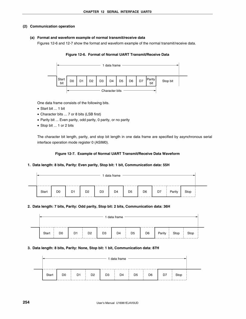
CHAPTER 12 SERIAL INTERFACE UART0
User’s Manual U16961EJ4V0UD 254
(2) Communication operation
(a) Format and waveform example of normal transmit/receive data
Figures 12-6 and 12-7 show the format and waveform example of the normal transmit/receive data.
Figure 12-6. Format of Normal UART Transmit/Receive Data
Start bit
Parity bit
D0 D1 D2 D3 D4
1 data frame
Character bits
D5 D6 D7 Stop bit
One data frame consists of the following bits.
• Start bit ... 1 bit
• Character bits ... 7 or 8 bits (LSB first)
• Parity bit ... Even parity, odd parity, 0 parity, or no parity
• Stop bit ... 1 or 2 bits
The character bit length, parity, and stop bit length in one data frame are specified by asynchronous serial
interface operation mode register 0 (ASIM0).
Figure 12-7. Example of Normal UART Transmit/Receive Data Waveform
1. Data length: 8 bits, Parity: Even parity, Stop bit: 1 bit, Communication data: 55H
1 data frame
Start D0 D1 D2 D3 D4 D5 D6 D7 Parity Stop
2. Data length: 7 bits, Parity: Odd parity, Stop bit: 2 bits, Communication data: 36H
1 data frame
Start D0 D1 D2 D3 D4 D5 D6 Parity StopStop
3. Data length: 8 bits, Parity: None, Stop bit: 1 bit, Communication data: 87H
1 data frame
Start D0 D1 D2 D3 D4 D5 D6 D7 Stop
CHAPTER 12 SERIAL INTERFACE UART0
User’s Manual U16961EJ4V0UD 255
(b) Parity types and operation
The parity bit is used to detect a bit error in communication data. Usually, the same type of parity bit is used
on both the transmission and reception sides. With even parity and odd parity, a 1-bit (odd number) error
can be detected. With zero parity and no parity, an error cannot be detected.
(i) Even parity
• Transmission
Transmit data, including the parity bit, is controlled so that the number of bits that are “1” is even.
The value of the parity bit is as follows.
If transmit data has an odd number of bits that are “1”: 1
If transmit data has an even number of bits that are “1”: 0
• Reception
The number of bits that are “1” in the receive data, including the parity bit, is counted. If it is odd, a
parity error occurs.
(ii) Odd parity
• Transmission
Unlike even parity, transmit data, including the parity bit, is controlled so that the number of bits that
are “1” is odd.
If transmit data has an odd number of bits that are “1”: 0
If transmit data has an even number of bits that are “1”: 1
• Reception
The number of bits that are “1” in the receive data, including the parity bit, is counted. If it is even, a
parity error occurs.
(iii) 0 parity
The parity bit is cleared to 0 when data is transmitted, regardless of the transmit data.
The parity bit is not detected when the data is received. Therefore, a parity error does not occur
regardless of whether the parity bit is “0” or “1”.
(iv) No parity
No parity bit is appended to the transmit data.
Reception is performed assuming that there is no parity bit when data is received. Because there is no
parity bit, a parity error does not occur.
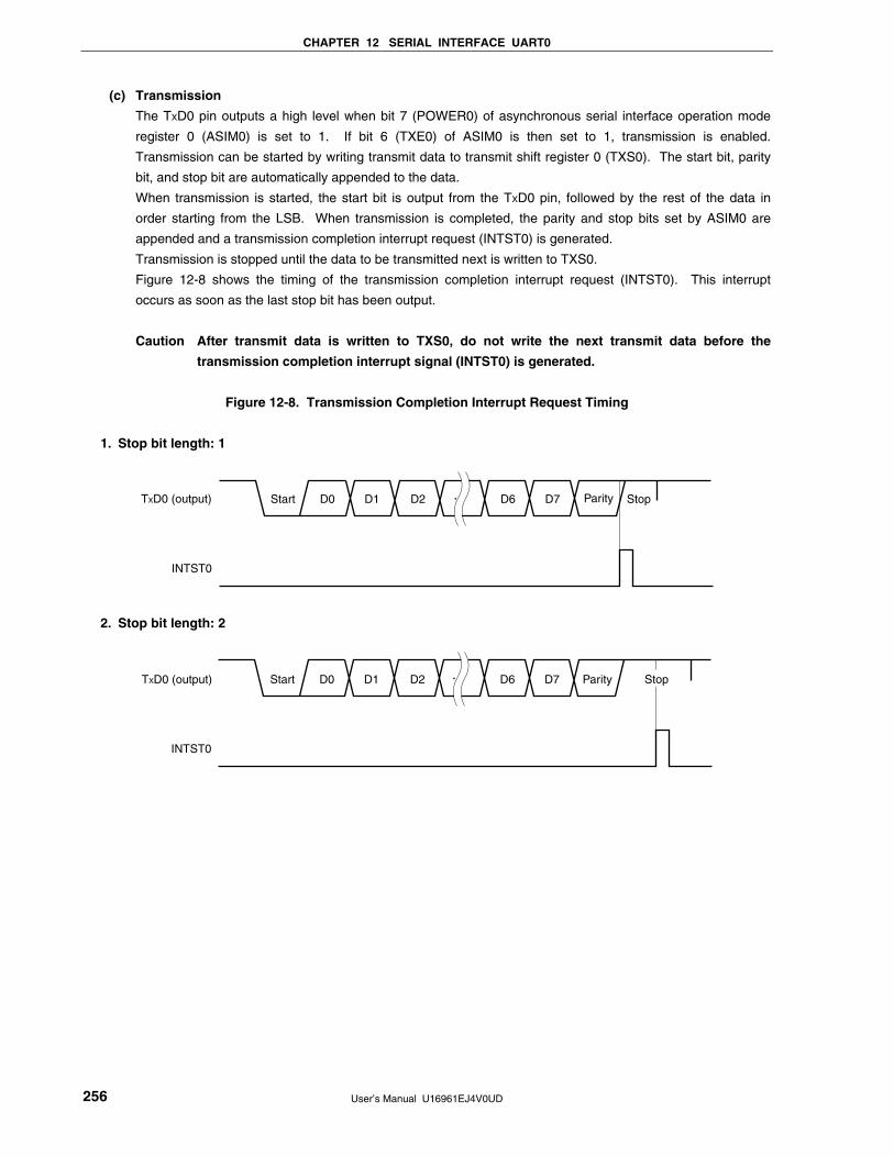
CHAPTER 12 SERIAL INTERFACE UART0
User’s Manual U16961EJ4V0UD 256
(c) Transmission
The TXD0 pin outputs a high level when bit 7 (POWER0) of asynchronous serial interface operation mode
register 0 (ASIM0) is set to 1. If bit 6 (TXE0) of ASIM0 is then set to 1, transmission is enabled.
Transmission can be started by writing transmit data to transmit shift register 0 (TXS0). The start bit, parity
bit, and stop bit are automatically appended to the data.
When transmission is started, the start bit is output from the TXD0 pin, followed by the rest of the data in
order starting from the LSB. When transmission is completed, the parity and stop bits set by ASIM0 are
appended and a transmission completion interrupt request (INTST0) is generated.
Transmission is stopped until the data to be transmitted next is written to TXS0.
Figure 12-8 shows the timing of the transmission completion interrupt request (INTST0). This interrupt
occurs as soon as the last stop bit has been output.
Caution After transmit data is written to TXS0, do not write the next transmit data before the
transmission completion interrupt signal (INTST0) is generated.
Figure 12-8. Transmission Completion Interrupt Request Timing
1. Stop bit length: 1
INTST0
D0Start D1 D2 D6 D7 StopTXD0 (output) Parity
2. Stop bit length: 2
TXD0 (output)
INTST0
D0Start D1 D2 D6 D7 Parity Stop
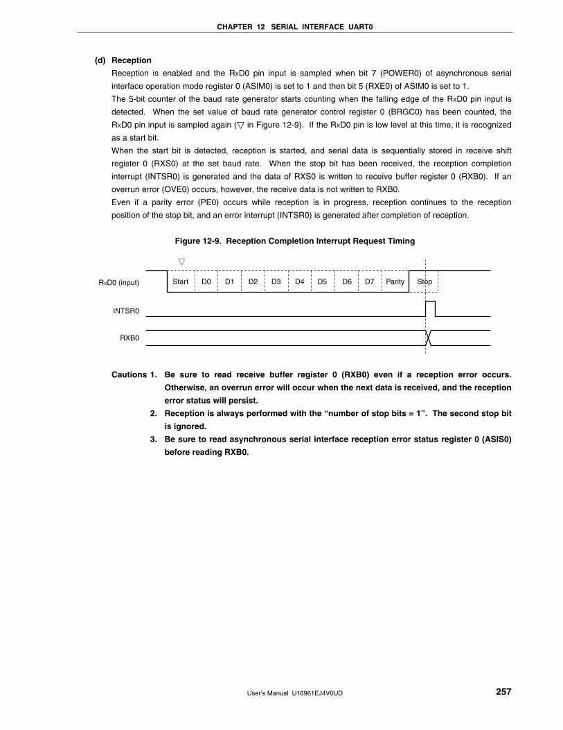
CHAPTER 12 SERIAL INTERFACE UART0
User’s Manual U16961EJ4V0UD 257
(d) Reception
Reception is enabled and the RXD0 pin input is sampled when bit 7 (POWER0) of asynchronous serial
interface operation mode register 0 (ASIM0) is set to 1 and then bit 5 (RXE0) of ASIM0 is set to 1.
The 5-bit counter of the baud rate generator starts counting when the falling edge of the RXD0 pin input is
detected. When the set value of baud rate generator control register 0 (BRGC0) has been counted, the
RXD0 pin input is sampled again ( in Figure 12-9). If the RXD0 pin is low level at this time, it is recognized
as a start bit.
When the start bit is detected, reception is started, and serial data is sequentially stored in receive shift
register 0 (RXS0) at the set baud rate. When the stop bit has been received, the reception completion
interrupt (INTSR0) is generated and the data of RXS0 is written to receive buffer register 0 (RXB0). If an
overrun error (OVE0) occurs, however, the receive data is not written to RXB0.
Even if a parity error (PE0) occurs while reception is in progress, reception continues to the reception
position of the stop bit, and an error interrupt (INTSR0) is generated after completion of reception.
Figure 12-9. Reception Completion Interrupt Request Timing
RXD0 (input)
INTSR0
Start D0 D1 D2 D3 D4 D5 D6 D7 Parity Stop
RXB0
Cautions 1. Be sure to read receive buffer register 0 (RXB0) even if a reception error occurs.
Otherwise, an overrun error will occur when the next data is received, and the reception
error status will persist.
2. Reception is always performed with the “number of stop bits = 1”. The second stop bit
is ignored.
3. Be sure to read asynchronous serial interface reception error status register 0 (ASIS0)
before reading RXB0.
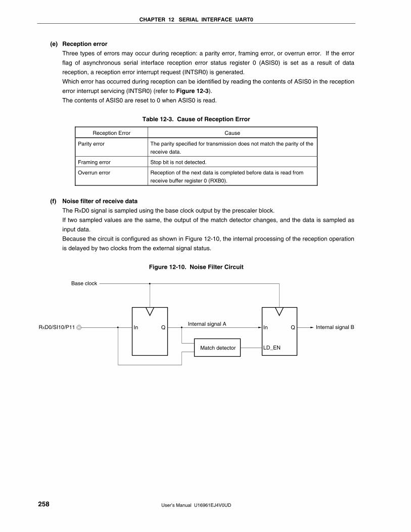
CHAPTER 12 SERIAL INTERFACE UART0
User’s Manual U16961EJ4V0UD 258
(e) Reception error
Three types of errors may occur during reception: a parity error, framing error, or overrun error. If the error
flag of asynchronous serial interface reception error status register 0 (ASIS0) is set as a result of data
reception, a reception error interrupt request (INTSR0) is generated.
Which error has occurred during reception can be identified by reading the contents of ASIS0 in the reception
error interrupt servicing (INTSR0) (refer to Figure 12-3).
The contents of ASIS0 are reset to 0 when ASIS0 is read.
Table 12-3. Cause of Reception Error
Reception Error Cause
Parity error The parity specified for transmission does not match the parity of the
receive data.
Framing error Stop bit is not detected.
Overrun error Reception of the next data is completed before data is read from
receive buffer register 0 (RXB0).
(f) Noise filter of receive data
The RXD0 signal is sampled using the base clock output by the prescaler block.
If two sampled values are the same, the output of the match detector changes, and the data is sampled as
input data.
Because the circuit is configured as shown in Figure 12-10, the internal processing of the reception operation
is delayed by two clocks from the external signal status.
Figure 12-10. Noise Filter Circuit
Internal signal BInternal signal A
Match detector
In
Base clock
RXD0/SI10/P11 Q In
LD_EN
Q
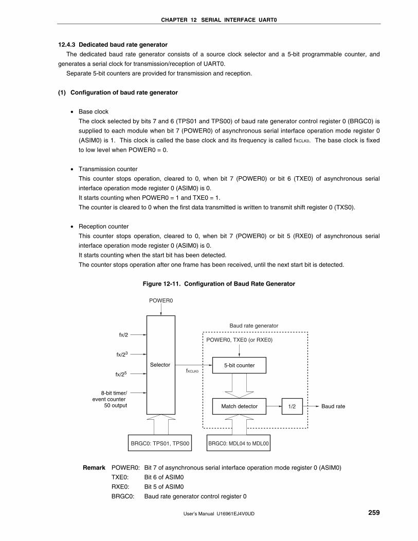
CHAPTER 12 SERIAL INTERFACE UART0
User’s Manual U16961EJ4V0UD 259
12.4.3 Dedicated baud rate generator
The dedicated baud rate generator consists of a source clock selector and a 5-bit programmable counter, and
generates a serial clock for transmission/reception of UART0.
Separate 5-bit counters are provided for transmission and reception.
(1) Configuration of baud rate generator
• Base clock
The clock selected by bits 7 and 6 (TPS01 and TPS00) of baud rate generator control register 0 (BRGC0) is
supplied to each module when bit 7 (POWER0) of asynchronous serial interface operation mode register 0
(ASIM0) is 1. This clock is called the base clock and its frequency is called fXCLK0. The base clock is fixed
to low level when POWER0 = 0.
• Transmission counter
This counter stops operation, cleared to 0, when bit 7 (POWER0) or bit 6 (TXE0) of asynchronous serial
interface operation mode register 0 (ASIM0) is 0.
It starts counting when POWER0 = 1 and TXE0 = 1.
The counter is cleared to 0 when the first data transmitted is written to transmit shift register 0 (TXS0).
• Reception counter
This counter stops operation, cleared to 0, when bit 7 (POWER0) or bit 5 (RXE0) of asynchronous serial
interface operation mode register 0 (ASIM0) is 0.
It starts counting when the start bit has been detected.
The counter stops operation after one frame has been received, until the next start bit is detected.
Figure 12-11. Configuration of Baud Rate Generator
fXCLK0
Selector
POWER0
5-bit counter
Match detector Baud rate
BRGC0: MDL04 to MDL00
1/2
POWER0, TXE0 (or RXE0)
BRGC0: TPS01, TPS00
8-bit timer/event counter
50 output
fX/25
fX/2
fX/23
Baud rate generator
Remark POWER0: Bit 7 of asynchronous serial interface operation mode register 0 (ASIM0)
TXE0: Bit 6 of ASIM0
RXE0: Bit 5 of ASIM0
BRGC0: Baud rate generator control register 0
CHAPTER 12 SERIAL INTERFACE UART0
User’s Manual U16961EJ4V0UD 260
(2) Generation of serial clock
A serial clock can be generated by using baud rate generator control register 0 (BRGC0).
Select the clock to be input to the 5-bit counter by using bits 7 and 6 (TPS01 and TPS00) of BRGC0.
Bits 4 to 0 (MDL04 to MDL00) of BRGC0 can be used to select the division value of the 5-bit counter.
(a) Baud rate
The baud rate can be calculated by the following expression.
• Baud rate = [bps]
Remark fXCLK0: Frequency of base clock selected by the TPS01 and TPS00 bits of the BRGC0 register
k: Value set by the MDL04 to MDL00 bits of the BRGC0 register (k = 8, 9, 10, ..., 31)
(b) Error of baud rate
The baud rate error can be calculated by the following expression.
• Error (%) = − 1 × 100 [%]
Cautions 1. Keep the baud rate error during transmission to within the permissible error range at
the reception destination.
2. Make sure that the baud rate error during reception satisfies the range shown in (4)
Permissible baud rate range during reception.
Example: Frequency of base clock = 2.5 MHz = 2,500,000 Hz
Set value of MDL04 to MDL00 bits of BRGC0 register = 10000B (k = 16)
Target baud rate = 76,800 bps
Baud rate = 2.5 M/(2 × 16)
= 2,500,000/(2 × 16) = 78,125 [bps]
Error = (78,125/76,800 − 1) × 100
= 1.725 [%]
fXCLK0
2 × k
Actual baud rate (baud rate with error)
Desired baud rate (correct baud rate)
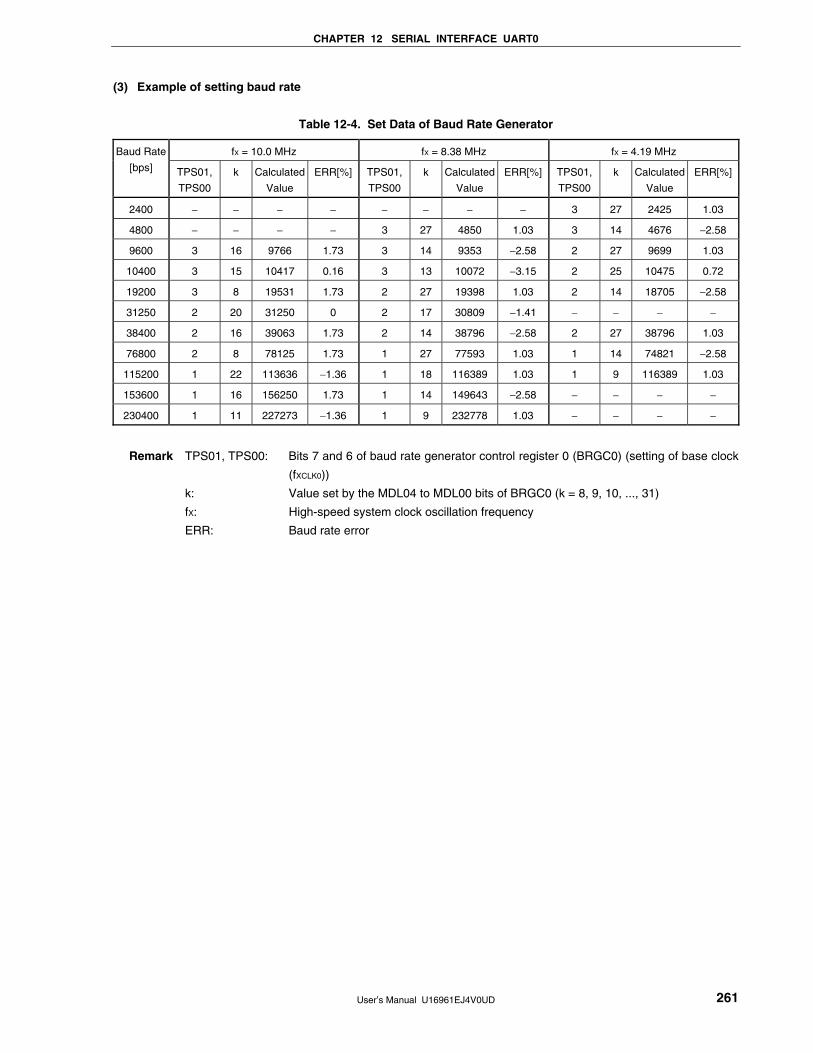
CHAPTER 12 SERIAL INTERFACE UART0
User’s Manual U16961EJ4V0UD 261
(3) Example of setting baud rate
Table 12-4. Set Data of Baud Rate Generator
fX = 10.0 MHz fX = 8.38 MHz fX = 4.19 MHz Baud Rate
[bps] TPS01,
TPS00
k Calculated
Value
ERR[%] TPS01,
TPS00
k Calculated
Value
ERR[%] TPS01,
TPS00
k Calculated
Value
ERR[%]
2400 − − − − − − − − 3 27 2425 1.03
4800 − − − − 3 27 4850 1.03 3 14 4676 −2.58
9600 3 16 9766 1.73 3 14 9353 −2.58 2 27 9699 1.03
10400 3 15 10417 0.16 3 13 10072 −3.15 2 25 10475 0.72
19200 3 8 19531 1.73 2 27 19398 1.03 2 14 18705 −2.58
31250 2 20 31250 0 2 17 30809 −1.41 − − − −
38400 2 16 39063 1.73 2 14 38796 −2.58 2 27 38796 1.03
76800 2 8 78125 1.73 1 27 77593 1.03 1 14 74821 −2.58
115200 1 22 113636 −1.36 1 18 116389 1.03 1 9 116389 1.03
153600 1 16 156250 1.73 1 14 149643 −2.58 − − − −
230400 1 11 227273 −1.36 1 9 232778 1.03 − − − −
Remark TPS01, TPS00: Bits 7 and 6 of baud rate generator control register 0 (BRGC0) (setting of base clock
(fXCLK0))
k: Value set by the MDL04 to MDL00 bits of BRGC0 (k = 8, 9, 10, ..., 31)
fX: High-speed system clock oscillation frequency
ERR: Baud rate error
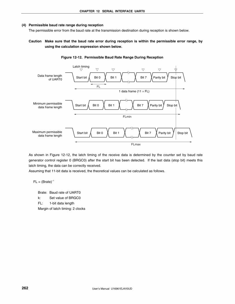
CHAPTER 12 SERIAL INTERFACE UART0
User’s Manual U16961EJ4V0UD 262
(4) Permissible baud rate range during reception
The permissible error from the baud rate at the transmission destination during reception is shown below.
Caution Make sure that the baud rate error during reception is within the permissible error range, by
using the calculation expression shown below.
Figure 12-12. Permissible Baud Rate Range During Reception
FL
1 data frame (11 × FL)
FLmin
FLmax
Data frame lengthof UART0
Start bit Bit 0 Bit 1 Bit 7 Parity bit
Minimum permissibledata frame length
Maximum permissibledata frame length
Stop bit
Start bit Bit 0 Bit 1 Bit 7 Parity bit
Latch timing
Stop bit
Start bit Bit 0 Bit 1 Bit 7 Parity bit Stop bit
As shown in Figure 12-12, the latch timing of the receive data is determined by the counter set by baud rate
generator control register 0 (BRGC0) after the start bit has been detected. If the last data (stop bit) meets this
latch timing, the data can be correctly received.
Assuming that 11-bit data is received, the theoretical values can be calculated as follows.
FL = (Brate)−1
Brate: Baud rate of UART0
k: Set value of BRGC0
FL: 1-bit data length
Margin of latch timing: 2 clocks

CHAPTER 12 SERIAL INTERFACE UART0
User’s Manual U16961EJ4V0UD 263
Minimum permissible data frame length: FLmin = 11 × FL − × FL = FL
Therefore, the maximum receivable baud rate at the transmission destination is as follows.
BRmax = (FLmin/11)−1 = Brate
Similarly, the maximum permissible data frame length can be calculated as follows.
10 k + 2 21k − 2
11 2 × k 2 × k
FLmax = FL × 11
Therefore, the minimum receivable baud rate at the transmission destination is as follows.
BRmin = (FLmax/11)−1 = Brate
The permissible baud rate error between UART0 and the transmission destination can be calculated from the
above minimum and maximum baud rate expressions, as follows.
Table 12-5. Maximum/Minimum Permissible Baud Rate Error
Division Ratio (k) Maximum Permissible Baud Rate Error Minimum Permissible Baud Rate Error
8 +3.53% −3.61%
16 +4.14% −4.19%
24 +4.34% −4.38%
31 +4.44% −4.47%
Remarks 1. The permissible error of reception depends on the number of bits in one frame, input clock
frequency, and division ratio (k). The higher the input clock frequency and the higher the division
ratio (k), the higher the permissible error.
2. k: Set value of BRGC0
k − 2
2k
21k + 2
2k
22k
21k + 2
× FLmax = 11 × FL − × FL = FL
21k – 2
20k
20k
21k − 2
User’s Manual U16961EJ4V0UD 264
CHAPTER 13 SERIAL INTERFACE UART6
13.1 Functions of Serial Interface UART6
Serial interface UART6 has the following two modes.
(1) Operation stop mode
This mode is used when serial communication is not executed and can enable a reduction in the power
consumption.
For details, see 13.4.1 Operation stop mode.
(2) Asynchronous serial interface (UART) mode
This mode supports the LIN (Local Interconnect Network)-bus. The functions of this mode are outlined below.
For details, see 13.4.2 Asynchronous serial interface (UART) mode and 13.4.3 Dedicated baud rate
generator.
• Two-pin configuration TXD6: Transmit data output pin
RXD6: Receive data input pin
• Data length of communication data can be selected from 7 or 8 bits.
• Dedicated internal 8-bit baud rate generator allowing any baud rate to be set
• Transmission and reception can be performed independently.
• Twelve operating clock inputs selectable
• MSB- or LSB-first communication selectable
• Inverted transmission operation
• Synchronous break field transmission from 13 to 20 bits
• More than 11 bits can be identified for synchronous break field reception (SBF reception flag provided).
Cautions 1. The TXD6 output inversion function inverts only the transmission side and not the reception
side. To use this function, the reception side must be ready for reception of inverted data.
2. If clock supply to serial interface UART6 is not stopped (e.g., in the HALT mode), normal
operation continues. If clock supply to serial interface UART6 is stopped (e.g., in the STOP
mode), each register stops operating, and holds the value immediately before clock supply
was stopped. The TXD6 pin also holds the value immediately before clock supply was
stopped and outputs it. However, the operation is not guaranteed after clock supply is
resumed. Therefore, reset the circuit so that POWER6 = 0, RXE6 = 0, and TXE6 = 0.
3. If data is continuously transmitted, the communication timing from the stop bit to the next
start bit is extended two operating clocks of the macro. However, this does not affect the
result of communication because the reception side initializes the timing when it has
detected a start bit. Do not use the continuous transmission function if UART6 is used in
the LIN communication operation.
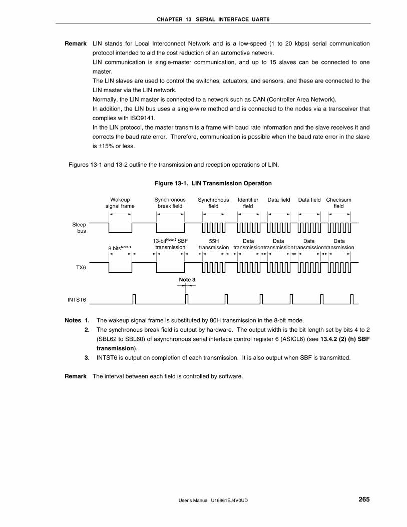
CHAPTER 13 SERIAL INTERFACE UART6
User’s Manual U16961EJ4V0UD 265
Remark LIN stands for Local Interconnect Network and is a low-speed (1 to 20 kbps) serial communication
protocol intended to aid the cost reduction of an automotive network.
LIN communication is single-master communication, and up to 15 slaves can be connected to one
master.
The LIN slaves are used to control the switches, actuators, and sensors, and these are connected to the
LIN master via the LIN network.
Normally, the LIN master is connected to a network such as CAN (Controller Area Network).
In addition, the LIN bus uses a single-wire method and is connected to the nodes via a transceiver that
complies with ISO9141.
In the LIN protocol, the master transmits a frame with baud rate information and the slave receives it and
corrects the baud rate error. Therefore, communication is possible when the baud rate error in the slave
is ±15% or less.
Figures 13-1 and 13-2 outline the transmission and reception operations of LIN.
Figure 13-1. LIN Transmission Operation
Sleepbus
Wakeupsignal frame
8 bitsNote 1
55Htransmission
Datatransmission
Datatransmission
Datatransmission
Datatransmission
13-bitNote 2 SBFtransmission
Note 3
Synchronousbreak field
Synchronousfield
Identifierfield
Data field Data field Checksumfield
TX6
INTST6
Notes 1. The wakeup signal frame is substituted by 80H transmission in the 8-bit mode.
2. The synchronous break field is output by hardware. The output width is the bit length set by bits 4 to 2
(SBL62 to SBL60) of asynchronous serial interface control register 6 (ASICL6) (see 13.4.2 (2) (h) SBF
transmission).
3. INTST6 is output on completion of each transmission. It is also output when SBF is transmitted.
Remark The interval between each field is controlled by software.
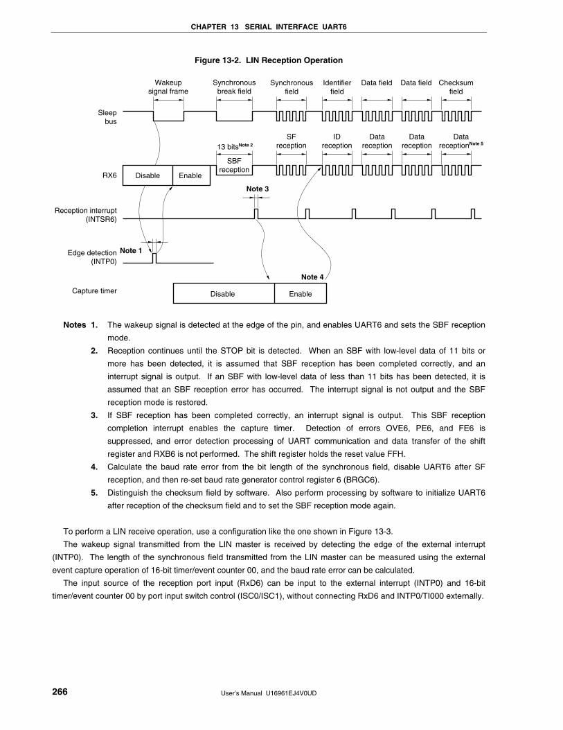
CHAPTER 13 SERIAL INTERFACE UART6
User’s Manual U16961EJ4V0UD 266
Figure 13-2. LIN Reception Operation
Sleepbus
13 bitsNote 2
SFreception
IDreception
Datareception
Datareception
DatareceptionNote 5
Note 3
Note 1
Note 4
Wakeupsignal frame
Synchronousbreak field
Synchronousfield
Identifierfield
Data field Data field Checksumfield
RX6
SBFreception
Reception interrupt(INTSR6)
Edge detection(INTP0)
Capture timer Disable Enable
Disable Enable
Notes 1. The wakeup signal is detected at the edge of the pin, and enables UART6 and sets the SBF reception
mode.
2. Reception continues until the STOP bit is detected. When an SBF with low-level data of 11 bits or
more has been detected, it is assumed that SBF reception has been completed correctly, and an
interrupt signal is output. If an SBF with low-level data of less than 11 bits has been detected, it is
assumed that an SBF reception error has occurred. The interrupt signal is not output and the SBF
reception mode is restored.
3. If SBF reception has been completed correctly, an interrupt signal is output. This SBF reception
completion interrupt enables the capture timer. Detection of errors OVE6, PE6, and FE6 is
suppressed, and error detection processing of UART communication and data transfer of the shift
register and RXB6 is not performed. The shift register holds the reset value FFH.
4. Calculate the baud rate error from the bit length of the synchronous field, disable UART6 after SF
reception, and then re-set baud rate generator control register 6 (BRGC6).
5. Distinguish the checksum field by software. Also perform processing by software to initialize UART6
after reception of the checksum field and to set the SBF reception mode again.
To perform a LIN receive operation, use a configuration like the one shown in Figure 13-3.
The wakeup signal transmitted from the LIN master is received by detecting the edge of the external interrupt
(INTP0). The length of the synchronous field transmitted from the LIN master can be measured using the external
event capture operation of 16-bit timer/event counter 00, and the baud rate error can be calculated.
The input source of the reception port input (RxD6) can be input to the external interrupt (INTP0) and 16-bit
timer/event counter 00 by port input switch control (ISC0/ISC1), without connecting RxD6 and INTP0/TI000 externally.
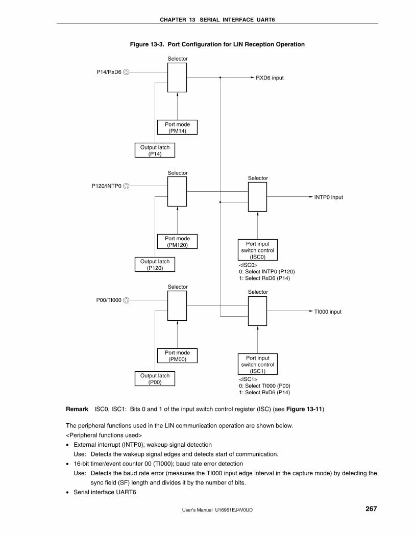
CHAPTER 13 SERIAL INTERFACE UART6
User’s Manual U16961EJ4V0UD 267
Figure 13-3. Port Configuration for LIN Reception Operation
RXD6 input
INTP0 input
TI000 input
P14/RxD6
P120/INTP0
P00/TI000
Port inputswitch control
(ISC0)
<ISC0>0: Select INTP0 (P120)1: Select RxD6 (P14)
Port mode(PM14)
Output latch(P14)
Port mode(PM120)
Output latch(P120)
Port inputswitch control
(ISC1)
<ISC1>0: Select TI000 (P00)1: Select RxD6 (P14)
SelectorSelector
Selector
Selector
Selector
Port mode(PM00)
Output latch(P00)
Remark ISC0, ISC1: Bits 0 and 1 of the input switch control register (ISC) (see Figure 13-11)
The peripheral functions used in the LIN communication operation are shown below.
<Peripheral functions used>
• External interrupt (INTP0); wakeup signal detection
Use: Detects the wakeup signal edges and detects start of communication.
• 16-bit timer/event counter 00 (TI000); baud rate error detection
Use: Detects the baud rate error (measures the TI000 input edge interval in the capture mode) by detecting the
sync field (SF) length and divides it by the number of bits.
• Serial interface UART6
CHAPTER 13 SERIAL INTERFACE UART6
User’s Manual U16961EJ4V0UD 268
13.2 Configuration of Serial Interface UART6
Serial interface UART6 includes the following hardware.
Table 13-1. Configuration of Serial Interface UART6
Item Configuration
Registers Receive buffer register 6 (RXB6)
Receive shift register 6 (RXS6)
Transmit buffer register 6 (TXB6)
Transmit shift register 6 (TXS6)
Control registers Asynchronous serial interface operation mode register 6 (ASIM6)
Asynchronous serial interface reception error status register 6 (ASIS6)
Asynchronous serial interface transmission status register 6 (ASIF6)
Clock selection register 6 (CKSR6)
Baud rate generator control register 6 (BRGC6)
Asynchronous serial interface control register 6 (ASICL6)
Input switch control register (ISC)
Port mode register 1 (PM1)
Port register 1 (P1)
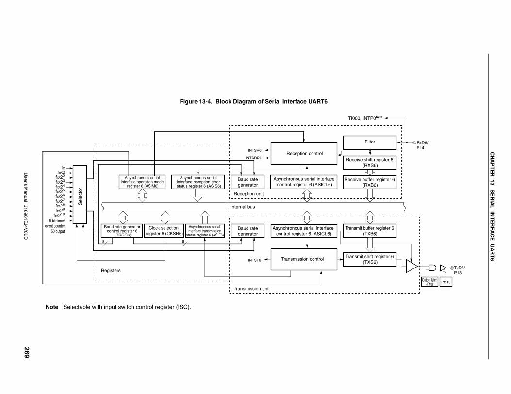
CH
AP
TE
R 13 S
ER
IAL
INT
ER
FA
CE
UA
RT
6
User’s M
anual U16961E
J4V0U
D
269
Figure 13-4. Block Diagram of Serial Interface UART6
Internal bus
Asynchronous serial interface control register 6 (ASICL6)
Transmit buffer register 6 (TXB6)
Transmit shift register 6 (TXS6)
TXD6/P13
INTST6
Baud rategenerator
Asynchronous serial interface control register 6 (ASICL6)
Reception controlReceive shift register 6
(RXS6)
Receive buffer register 6 (RXB6)
RXD6/P14
TI000, INTP0Note
INTSR6
Baud rategenerator
Filter
INTSRE6
Asynchronous serial interface reception error status register 6 (ASIS6)
Asynchronous serial interface operation mode
register 6 (ASIM6)
Asynchronous serial interface transmission
status register 6 (ASIF6)
Transmission control
Registers
fXfX/2
fX/22
fX/23
fX/24
fX/25
fX/26
fX/27
fX/28
fX/29
fX/210
8-bit timer/event counter
50 output
8
Reception unit
Transmission unit
Clock selection register 6 (CKSR6)
Baud rate generator control register 6
(BRGC6)
Output latch(P13) PM13
8
Sel
ecto
r
Note Selectable with input switch control register (ISC).
CHAPTER 13 SERIAL INTERFACE UART6
User’s Manual U16961EJ4V0UD 270
(1) Receive buffer register 6 (RXB6)
This 8-bit register stores parallel data converted by receive shift register 6 (RXS6).
Each time 1 byte of data has been received, new receive data is transferred to this register from receive shift
register 6 (RXS6). If the data length is set to 7 bits, data is transferred as follows.
• In LSB-first reception, the receive data is transferred to bits 0 to 6 of RXB6 and the MSB of RXB6 is always 0.
• In MSB-first reception, the receive data is transferred to bits 1 to 7 of RXB6 and the LSB of RXB6 is always 0.
If an overrun error (OVE6) occurs, the receive data is not transferred to RXB6.
RXB6 can be read by an 8-bit memory manipulation instruction. No data can be written to this register.
RESET input sets this register to FFH.
(2) Receive shift register 6 (RXS6)
This register converts the serial data input to the RXD6 pin into parallel data.
RXS6 cannot be directly manipulated by a program.
(3) Transmit buffer register 6 (TXB6)
This buffer register is used to set transmit data. Transmission is started when data is written to TXB6.
This register can be read or written by an 8-bit memory manipulation instruction.
RESET input sets this register to FFH.
Cautions 1. Do not write data to TXB6 when bit 1 (TXBF6) of asynchronous serial interface transmission
status register 6 (ASIF6) is 1.
2. Do not refresh (write the same value to) TXB6 by software during a communication
operation (when bit 7 (POWER6) and bit 6 (TXE6) of asynchronous serial interface operation
mode register 6 (ASIM6) are 1 or when bit 7 (POWER6) and bit 5 (RXE6) of ASIM6 are 1).
(4) Transmit shift register 6 (TXS6)
This register transmits the data transferred from TXB6 from the TXD6 pin as serial data. Data is transferred from
TXB6 immediately after TXB6 is written for the first transmission, or immediately before INTST6 occurs after one
frame was transmitted for continuous transmission. Data is transferred from TXB6 and transmitted from the TXD6
pin at the falling edge of the base clock.
TXS6 cannot be directly manipulated by a program.
CHAPTER 13 SERIAL INTERFACE UART6
User’s Manual U16961EJ4V0UD 271
13.3 Registers Controlling Serial Interface UART6
Serial interface UART6 is controlled by the following nine registers.
• Asynchronous serial interface operation mode register 6 (ASIM6)
• Asynchronous serial interface reception error status register 6 (ASIS6)
• Asynchronous serial interface transmission status register 6 (ASIF6)
• Clock selection register 6 (CKSR6)
• Baud rate generator control register 6 (BRGC6)
• Asynchronous serial interface control register 6 (ASICL6)
• Input switch control register (ISC)
• Port mode register 1 (PM1)
• Port register 1 (P1)
(1) Asynchronous serial interface operation mode register 6 (ASIM6)
This 8-bit register controls the serial communication operations of serial interface UART6.
This register can be set by a 1-bit or 8-bit memory manipulation instruction.
RESET input sets this register to 01H.
Remark ASIM6 can be refreshed (the same value is written) by software during a communication operation
(when bit 7 (POWER6) and bit 6 (TXE6) of ASIM6 = 1 or bit 7 (POWER6) and bit 5 (RXE6) of ASIM6
= 1).
Figure 13-5. Format of Asynchronous Serial Interface Operation Mode Register 6 (ASIM6) (1/2)
Address: FF50H After reset: 01H R/W
Symbol <7> <6> <5> 4 3 2 1 0
ASIM6 POWER6 TXE6 RXE6 PS61 PS60 CL6 SL6 ISRM6
POWER6 Enables/disables operation of internal operation clock
0Note 1 Disables operation of the internal operation clock (fixes the clock to low level) and asynchronously
resets the internal circuitNote 2.
1Note 3 Enables operation of the internal operation clock
TXE6 Enables/disables transmission
0 Disables transmission (synchronously resets the transmission circuit).
1 Enables transmission
Notes 1. The output of the TXD6 pin goes high and the input from the RXD6 pin is fixed to high level when
POWER6 = 0.
2. Asynchronous serial interface reception error status register 6 (ASIS6), asynchronous serial interface
transmission status register 6 (ASIF6), bit 7 (SBRF6) and bit 6 (SBRT6) of asynchronous serial
interface control register 6 (ASICL6), and receive buffer register 6 (RXB6) are reset.
3. Operation of the 8-bit counter output is enabled at the second base clock after 1 is written to the
POWER6 bit.
CHAPTER 13 SERIAL INTERFACE UART6
User’s Manual U16961EJ4V0UD 272
Figure 13-5. Format of Asynchronous Serial Interface Operation Mode Register 6 (ASIM6) (2/2)
RXE6 Enables/disables reception
0 Disables reception (synchronously resets the reception circuit).
1 Enables reception
PS61 PS60 Transmission operation Reception operation
0 0 Does not output parity bit. Reception without parity
0 1 Outputs 0 parity. Reception as 0 parityNote
1 0 Outputs odd parity. Judges as odd parity.
1 1 Outputs even parity. Judges as even parity.
CL6 Specifies character length of transmit/receive data
0 Character length of data = 7 bits
1 Character length of data = 8 bits
SL6 Specifies number of stop bits of transmit data
0 Number of stop bits = 1
1 Number of stop bits = 2
ISRM6 Enables/disables occurrence of reception completion interrupt in case of error
0 “INTSRE6” occurs in case of error (at this time, INTSR6 does not occur).
1 “INTSR6” occurs in case of error (at this time, INTSRE6 does not occur).
Note If “reception as 0 parity” is selected, the parity is not judged. Therefore, bit 2 (PE6) of asynchronous serial
interface reception error status register 6 (ASIS6) is not set and the error interrupt does not occur.
Cautions 1. At startup, set POWER6 to 1 and then set TXE6 to 1. To stop the operation, clear TXE6 to 0,
and then clear POWER6 to 0.
2. At startup, set POWER6 to 1 and then set RXE6 to 1. To stop the operation, clear RXE6 to 0,
and then clear POWER6 to 0.
3. Set POWER6 to 1 and then set RXE6 to 1 while a high level is input to the RxD6 pin. If
POWER6 is set to 1 and RXE6 is set to 1 while a low level is input, reception is started.
4. Clear the TXE6 and RXE6 bits to 0 before rewriting the PS61, PS60, and CL6 bits.
5. Fix the PS61 and PS60 bits to 0 when the UART6 is used in the LIN communication operation.
6. Make sure that TXE6 = 0 when rewriting the SL6 bit. Reception is always performed with “the
number of stop bits = 1”, and therefore, is not affected by the set value of the SL6 bit.
7. Make sure that RXE6 = 0 when rewriting the ISRM6 bit.
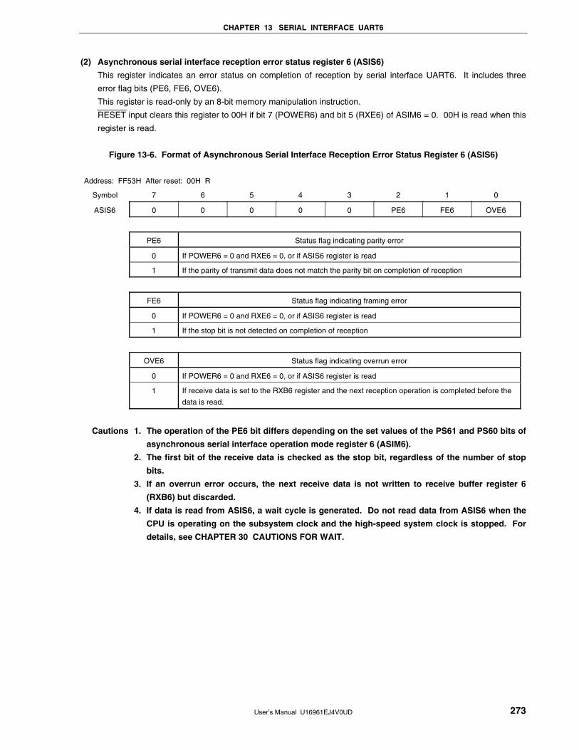
CHAPTER 13 SERIAL INTERFACE UART6
User’s Manual U16961EJ4V0UD 273
(2) Asynchronous serial interface reception error status register 6 (ASIS6)
This register indicates an error status on completion of reception by serial interface UART6. It includes three
error flag bits (PE6, FE6, OVE6).
This register is read-only by an 8-bit memory manipulation instruction.
RESET input clears this register to 00H if bit 7 (POWER6) and bit 5 (RXE6) of ASIM6 = 0. 00H is read when this
register is read.
Figure 13-6. Format of Asynchronous Serial Interface Reception Error Status Register 6 (ASIS6)
Address: FF53H After reset: 00H R
Symbol 7 6 5 4 3 2 1 0
ASIS6 0 0 0 0 0 PE6 FE6 OVE6
PE6 Status flag indicating parity error
0 If POWER6 = 0 and RXE6 = 0, or if ASIS6 register is read
1 If the parity of transmit data does not match the parity bit on completion of reception
FE6 Status flag indicating framing error
0 If POWER6 = 0 and RXE6 = 0, or if ASIS6 register is read
1 If the stop bit is not detected on completion of reception
OVE6 Status flag indicating overrun error
0 If POWER6 = 0 and RXE6 = 0, or if ASIS6 register is read
1 If receive data is set to the RXB6 register and the next reception operation is completed before the
data is read.
Cautions 1. The operation of the PE6 bit differs depending on the set values of the PS61 and PS60 bits of
asynchronous serial interface operation mode register 6 (ASIM6).
2. The first bit of the receive data is checked as the stop bit, regardless of the number of stop
bits.
3. If an overrun error occurs, the next receive data is not written to receive buffer register 6
(RXB6) but discarded.
4. If data is read from ASIS6, a wait cycle is generated. Do not read data from ASIS6 when the
CPU is operating on the subsystem clock and the high-speed system clock is stopped. For
details, see CHAPTER 30 CAUTIONS FOR WAIT.
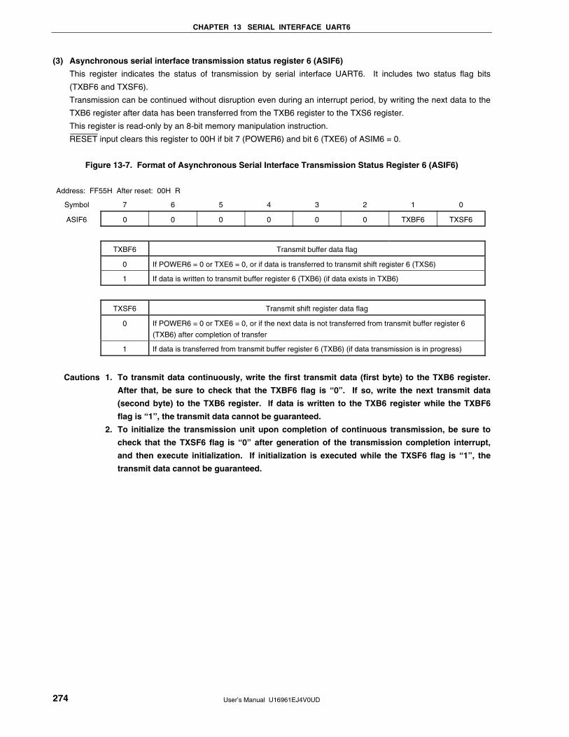
CHAPTER 13 SERIAL INTERFACE UART6
User’s Manual U16961EJ4V0UD 274
(3) Asynchronous serial interface transmission status register 6 (ASIF6)
This register indicates the status of transmission by serial interface UART6. It includes two status flag bits
(TXBF6 and TXSF6).
Transmission can be continued without disruption even during an interrupt period, by writing the next data to the
TXB6 register after data has been transferred from the TXB6 register to the TXS6 register.
This register is read-only by an 8-bit memory manipulation instruction.
RESET input clears this register to 00H if bit 7 (POWER6) and bit 6 (TXE6) of ASIM6 = 0.
Figure 13-7. Format of Asynchronous Serial Interface Transmission Status Register 6 (ASIF6)
Address: FF55H After reset: 00H R
Symbol 7 6 5 4 3 2 1 0
ASIF6 0 0 0 0 0 0 TXBF6 TXSF6
TXBF6 Transmit buffer data flag
0 If POWER6 = 0 or TXE6 = 0, or if data is transferred to transmit shift register 6 (TXS6)
1 If data is written to transmit buffer register 6 (TXB6) (if data exists in TXB6)
TXSF6 Transmit shift register data flag
0 If POWER6 = 0 or TXE6 = 0, or if the next data is not transferred from transmit buffer register 6
(TXB6) after completion of transfer
1 If data is transferred from transmit buffer register 6 (TXB6) (if data transmission is in progress)
Cautions 1. To transmit data continuously, write the first transmit data (first byte) to the TXB6 register.
After that, be sure to check that the TXBF6 flag is “0”. If so, write the next transmit data
(second byte) to the TXB6 register. If data is written to the TXB6 register while the TXBF6
flag is “1”, the transmit data cannot be guaranteed.
2. To initialize the transmission unit upon completion of continuous transmission, be sure to
check that the TXSF6 flag is “0” after generation of the transmission completion interrupt,
and then execute initialization. If initialization is executed while the TXSF6 flag is “1”, the
transmit data cannot be guaranteed.
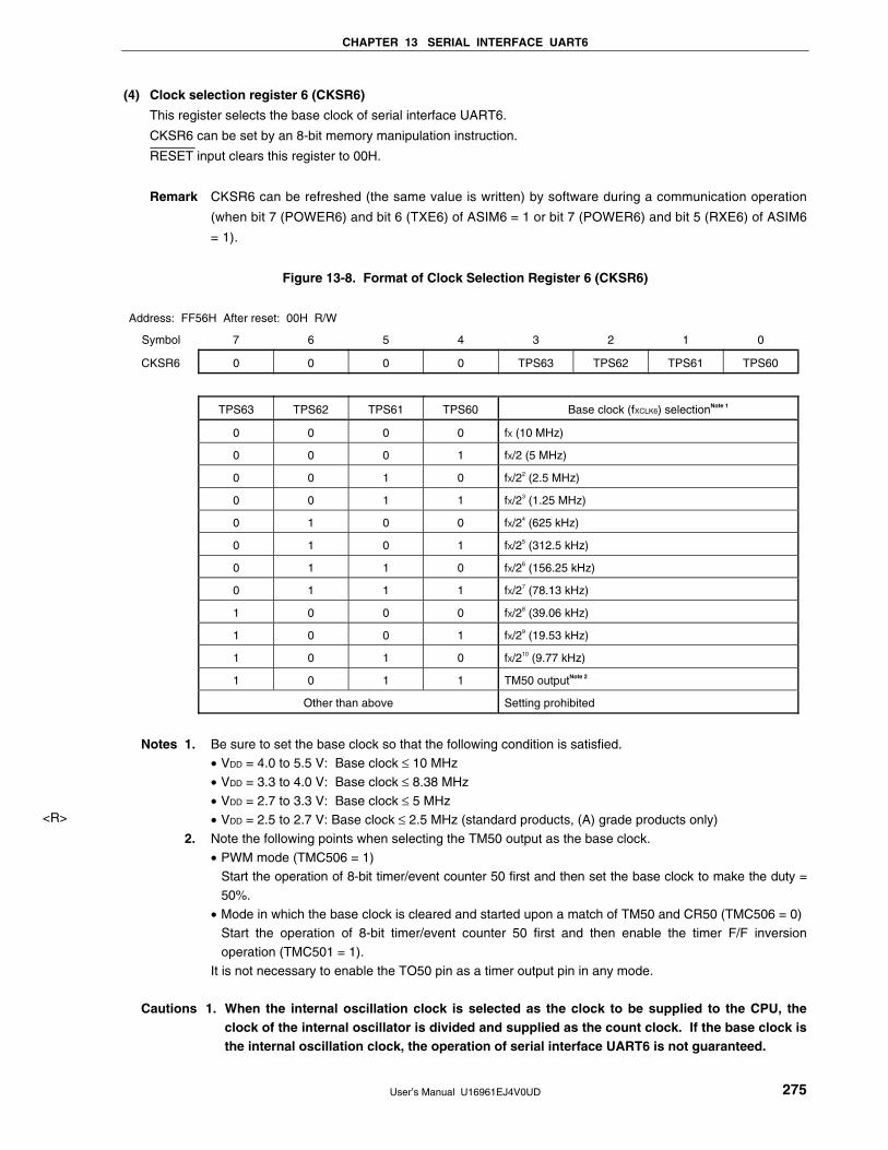
CHAPTER 13 SERIAL INTERFACE UART6
User’s Manual U16961EJ4V0UD 275
(4) Clock selection register 6 (CKSR6)
This register selects the base clock of serial interface UART6.
CKSR6 can be set by an 8-bit memory manipulation instruction.
RESET input clears this register to 00H.
Remark CKSR6 can be refreshed (the same value is written) by software during a communication operation
(when bit 7 (POWER6) and bit 6 (TXE6) of ASIM6 = 1 or bit 7 (POWER6) and bit 5 (RXE6) of ASIM6
= 1).
Figure 13-8. Format of Clock Selection Register 6 (CKSR6)
Address: FF56H After reset: 00H R/W
Symbol 7 6 5 4 3 2 1 0
CKSR6 0 0 0 0 TPS63 TPS62 TPS61 TPS60
TPS63 TPS62 TPS61 TPS60 Base clock (fXCLK6) selectionNote 1
0 0 0 0 fX (10 MHz)
0 0 0 1 fX/2 (5 MHz)
0 0 1 0 fX/22 (2.5 MHz)
0 0 1 1 fX/23 (1.25 MHz)
0 1 0 0 fX/24 (625 kHz)
0 1 0 1 fX/25 (312.5 kHz)
0 1 1 0 fX/26 (156.25 kHz)
0 1 1 1 fX/27 (78.13 kHz)
1 0 0 0 fX/28 (39.06 kHz)
1 0 0 1 fX/29 (19.53 kHz)
1 0 1 0 fX/210 (9.77 kHz)
1 0 1 1 TM50 outputNote 2
Other than above Setting prohibited
Notes 1. Be sure to set the base clock so that the following condition is satisfied. • VDD = 4.0 to 5.5 V: Base clock ≤ 10 MHz
• VDD = 3.3 to 4.0 V: Base clock ≤ 8.38 MHz
• VDD = 2.7 to 3.3 V: Base clock ≤ 5 MHz • VDD = 2.5 to 2.7 V: Base clock ≤ 2.5 MHz (standard products, (A) grade products only)
2. Note the following points when selecting the TM50 output as the base clock.
• PWM mode (TMC506 = 1) Start the operation of 8-bit timer/event counter 50 first and then set the base clock to make the duty =
50%.
• Mode in which the base clock is cleared and started upon a match of TM50 and CR50 (TMC506 = 0) Start the operation of 8-bit timer/event counter 50 first and then enable the timer F/F inversion
operation (TMC501 = 1).
It is not necessary to enable the TO50 pin as a timer output pin in any mode. Cautions 1. When the internal oscillation clock is selected as the clock to be supplied to the CPU, the
clock of the internal oscillator is divided and supplied as the count clock. If the base clock is the internal oscillation clock, the operation of serial interface UART6 is not guaranteed.
<R>

CHAPTER 13 SERIAL INTERFACE UART6
User’s Manual U16961EJ4V0UD 276
Cautions 2. Make sure POWER6 = 0 when rewriting TPS63 to TPS60.
Remarks 1. Figures in parentheses are for operation with fX = 10 MHz.
2. fX: High-speed system clock oscillation frequency
3. TMC506: Bit 6 of 8-bit timer mode control register 50 (TMC50)
TMC501: Bit 1 of TMC50
(5) Baud rate generator control register 6 (BRGC6)
This register sets the division value of the 8-bit counter of serial interface UART6.
BRGC6 can be set by an 8-bit memory manipulation instruction.
RESET input sets this register to FFH.
Remark BRGC6 can be refreshed (the same value is written) by software during a communication operation
(when bit 7 (POWER6) and bit 6 (TXE6) of ASIM6 = 1 or bit 7 (POWER6) and bit 5 (RXE6) of ASIM6
= 1).
Figure 13-9. Format of Baud Rate Generator Control Register 6 (BRGC6)
Address: FF57H After reset: FFH R/W
Symbol 7 6 5 4 3 2 1 0
BRGC6 MDL67 MDL66 MDL65 MDL64 MDL63 MDL62 MDL61 MDL60
MDL67 MDL66 MDL65 MDL64 MDL63 MDL62 MDL61 MDL60 k Output clock selection of
8-bit counter
0 0 0 0 0 × × × × Setting prohibited
0 0 0 0 1 0 0 0 8 fXCLK6/8
0 0 0 0 1 0 0 1 9 fXCLK6/9
0 0 0 0 1 0 1 0 10 fXCLK6/10
•
•
•
•
•
•
•
•
•
•
•
•
•
•
•
•
•
•
•
•
•
•
•
•
•
•
•
•
•
•
•
•
•
•
•
•
•
•
•
•
•
•
•
•
•
•
•
•
•
•
1 1 1 1 1 1 0 0 252 fXCLK6/252
1 1 1 1 1 1 0 1 253 fXCLK6/253
1 1 1 1 1 1 1 0 254 fXCLK6/254
1 1 1 1 1 1 1 1 255 fXCLK6/255
Cautions 1. Make sure that bit 6 (TXE6) and bit 5 (RXE6) of the ASIM6 register = 0 when rewriting the
MDL67 to MDL60 bits.
2. The baud rate is the output clock of the 8-bit counter divided by 2.
Remarks 1. fXCLK6: Frequency of base clock selected by the TPS63 to TPS60 bits of CKSR6 register
2. k: Value set by MDL67 to MDL60 bits (k = 8, 9, 10, ..., 255)
3. ×: Don’t care
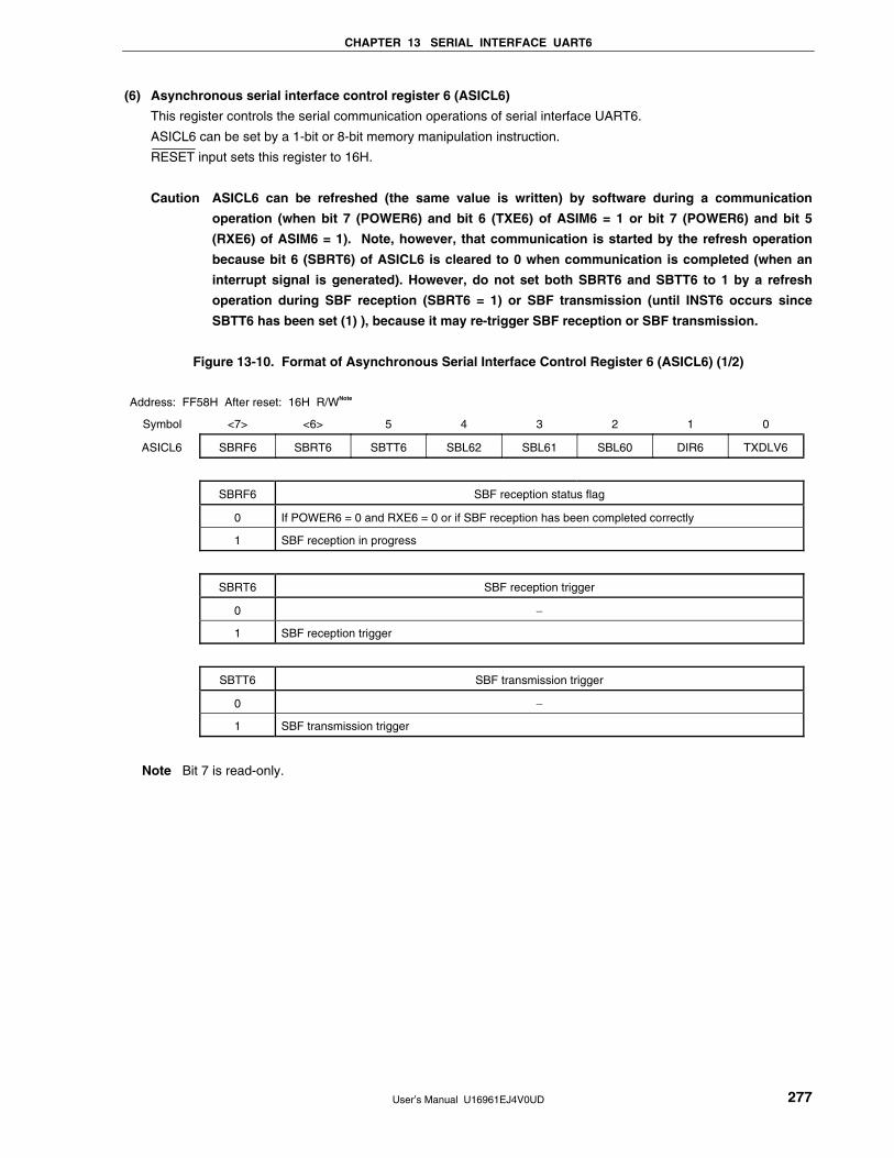
CHAPTER 13 SERIAL INTERFACE UART6
User’s Manual U16961EJ4V0UD 277
(6) Asynchronous serial interface control register 6 (ASICL6)
This register controls the serial communication operations of serial interface UART6.
ASICL6 can be set by a 1-bit or 8-bit memory manipulation instruction.
RESET input sets this register to 16H.
Caution ASICL6 can be refreshed (the same value is written) by software during a communication
operation (when bit 7 (POWER6) and bit 6 (TXE6) of ASIM6 = 1 or bit 7 (POWER6) and bit 5
(RXE6) of ASIM6 = 1). Note, however, that communication is started by the refresh operation
because bit 6 (SBRT6) of ASICL6 is cleared to 0 when communication is completed (when an
interrupt signal is generated). However, do not set both SBRT6 and SBTT6 to 1 by a refresh
operation during SBF reception (SBRT6 = 1) or SBF transmission (until INST6 occurs since
SBTT6 has been set (1) ), because it may re-trigger SBF reception or SBF transmission.
Figure 13-10. Format of Asynchronous Serial Interface Control Register 6 (ASICL6) (1/2)
Address: FF58H After reset: 16H R/WNote
Symbol <7> <6> 5 4 3 2 1 0
ASICL6 SBRF6 SBRT6 SBTT6 SBL62 SBL61 SBL60 DIR6 TXDLV6
SBRF6 SBF reception status flag
0 If POWER6 = 0 and RXE6 = 0 or if SBF reception has been completed correctly
1 SBF reception in progress
SBRT6 SBF reception trigger
0 −
1 SBF reception trigger
SBTT6 SBF transmission trigger
0 −
1 SBF transmission trigger
Note Bit 7 is read-only.
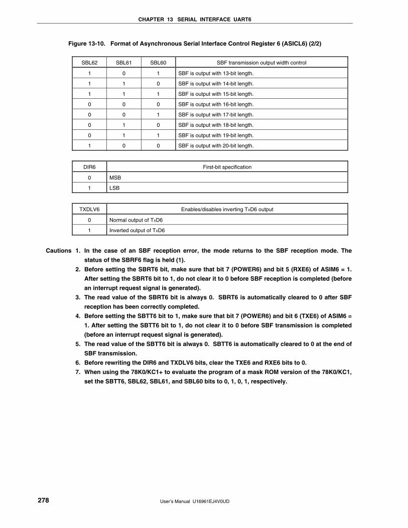
CHAPTER 13 SERIAL INTERFACE UART6
User’s Manual U16961EJ4V0UD 278
Figure 13-10. Format of Asynchronous Serial Interface Control Register 6 (ASICL6) (2/2)
SBL62 SBL61 SBL60 SBF transmission output width control
1 0 1 SBF is output with 13-bit length.
1 1 0 SBF is output with 14-bit length.
1 1 1 SBF is output with 15-bit length.
0 0 0 SBF is output with 16-bit length.
0 0 1 SBF is output with 17-bit length.
0 1 0 SBF is output with 18-bit length.
0 1 1 SBF is output with 19-bit length.
1 0 0 SBF is output with 20-bit length.
DIR6 First-bit specification
0 MSB
1 LSB
TXDLV6 Enables/disables inverting TXD6 output
0 Normal output of TXD6
1 Inverted output of TXD6
Cautions 1. In the case of an SBF reception error, the mode returns to the SBF reception mode. The
status of the SBRF6 flag is held (1).
2. Before setting the SBRT6 bit, make sure that bit 7 (POWER6) and bit 5 (RXE6) of ASIM6 = 1.
After setting the SBRT6 bit to 1, do not clear it to 0 before SBF reception is completed (before
an interrupt request signal is generated).
3. The read value of the SBRT6 bit is always 0. SBRT6 is automatically cleared to 0 after SBF
reception has been correctly completed.
4. Before setting the SBTT6 bit to 1, make sure that bit 7 (POWER6) and bit 6 (TXE6) of ASIM6 =
1. After setting the SBTT6 bit to 1, do not clear it to 0 before SBF transmission is completed
(before an interrupt request signal is generated).
5. The read value of the SBTT6 bit is always 0. SBTT6 is automatically cleared to 0 at the end of
SBF transmission.
6. Before rewriting the DIR6 and TXDLV6 bits, clear the TXE6 and RXE6 bits to 0.
7. When using the 78K0/KC1+ to evaluate the program of a mask ROM version of the 78K0/KC1,
set the SBTT6, SBL62, SBL61, and SBL60 bits to 0, 1, 0, 1, respectively.
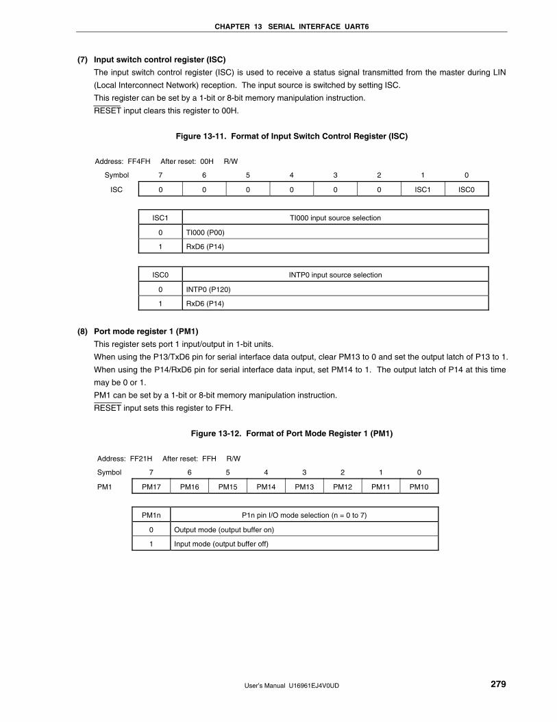
CHAPTER 13 SERIAL INTERFACE UART6
User’s Manual U16961EJ4V0UD 279
(7) Input switch control register (ISC)
The input switch control register (ISC) is used to receive a status signal transmitted from the master during LIN
(Local Interconnect Network) reception. The input source is switched by setting ISC.
This register can be set by a 1-bit or 8-bit memory manipulation instruction.
RESET input clears this register to 00H.
Figure 13-11. Format of Input Switch Control Register (ISC)
Address: FF4FH After reset: 00H R/W
Symbol 7 6 5 4 3 2 1 0
ISC 0 0 0 0 0 0 ISC1 ISC0
ISC1 TI000 input source selection
0 TI000 (P00)
1 RxD6 (P14)
ISC0 INTP0 input source selection
0 INTP0 (P120)
1 RxD6 (P14)
(8) Port mode register 1 (PM1)
This register sets port 1 input/output in 1-bit units.
When using the P13/TxD6 pin for serial interface data output, clear PM13 to 0 and set the output latch of P13 to 1.
When using the P14/RxD6 pin for serial interface data input, set PM14 to 1. The output latch of P14 at this time
may be 0 or 1.
PM1 can be set by a 1-bit or 8-bit memory manipulation instruction.
RESET input sets this register to FFH.
Figure 13-12. Format of Port Mode Register 1 (PM1)
Address: FF21H After reset: FFH R/W
Symbol 7 6 5 4 3 2 1 0
PM1 PM17 PM16 PM15 PM14 PM13 PM12 PM11 PM10
PM1n P1n pin I/O mode selection (n = 0 to 7)
0 Output mode (output buffer on)
1 Input mode (output buffer off)
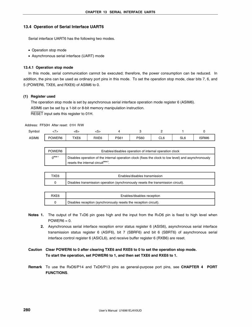
CHAPTER 13 SERIAL INTERFACE UART6
User’s Manual U16961EJ4V0UD 280
13.4 Operation of Serial Interface UART6
Serial interface UART6 has the following two modes.
• Operation stop mode
• Asynchronous serial interface (UART) mode
13.4.1 Operation stop mode
In this mode, serial communication cannot be executed; therefore, the power consumption can be reduced. In
addition, the pins can be used as ordinary port pins in this mode. To set the operation stop mode, clear bits 7, 6, and
5 (POWER6, TXE6, and RXE6) of ASIM6 to 0.
(1) Register used
The operation stop mode is set by asynchronous serial interface operation mode register 6 (ASIM6).
ASIM6 can be set by a 1-bit or 8-bit memory manipulation instruction.
RESET input sets this register to 01H.
Address: FF50H After reset: 01H R/W
Symbol <7> <6> <5> 4 3 2 1 0
ASIM6 POWER6 TXE6 RXE6 PS61 PS60 CL6 SL6 ISRM6
POWER6 Enables/disables operation of internal operation clock
0Note 1 Disables operation of the internal operation clock (fixes the clock to low level) and asynchronously
resets the internal circuitNote 2.
TXE6 Enables/disables transmission
0 Disables transmission operation (synchronously resets the transmission circuit).
RXE6 Enables/disables reception
0 Disables reception (synchronously resets the reception circuit).
Notes 1. The output of the TXD6 pin goes high and the input from the RXD6 pin is fixed to high level when
POWER6 = 0.
2. Asynchronous serial interface reception error status register 6 (ASIS6), asynchronous serial interface
transmission status register 6 (ASIF6), bit 7 (SBRF6) and bit 6 (SBRT6) of asynchronous serial
interface control register 6 (ASICL6), and receive buffer register 6 (RXB6) are reset.
Caution Clear POWER6 to 0 after clearing TXE6 and RXE6 to 0 to set the operation stop mode.
To start the operation, set POWER6 to 1, and then set TXE6 and RXE6 to 1.
Remark To use the RxD6/P14 and TxD6/P13 pins as general-purpose port pins, see CHAPTER 4 PORT
FUNCTIONS.
CHAPTER 13 SERIAL INTERFACE UART6
User’s Manual U16961EJ4V0UD 281
13.4.2 Asynchronous serial interface (UART) mode
In this mode, data of 1 byte is transmitted/received following a start bit, and a full-duplex operation can be
performed.
A dedicated UART baud rate generator is incorporated, so that communication can be executed at a wide range of
baud rates.
(1) Registers used
• Asynchronous serial interface operation mode register 6 (ASIM6)
• Asynchronous serial interface reception error status register 6 (ASIS6)
• Asynchronous serial interface transmission status register 6 (ASIF6)
• Clock selection register 6 (CKSR6)
• Baud rate generator control register 6 (BRGC6)
• Asynchronous serial interface control register 6 (ASICL6)
• Input switch control register (ISC)
• Port mode register 1 (PM1)
• Port register 1 (P1)
The basic procedure of setting an operation in the UART mode is as follows.
<1> Set the CKSR6 register (see Figure 13-8).
<2> Set the BRGC6 register (see Figure 13-9).
<3> Set bits 0 to 4 (ISRM6, SL6, CL6, PS60, PS61) of the ASIM6 register (see Figure 13-5).
<4> Set bits 0 and 1 (TXDLV6, DIR6) of the ASICL6 register (see Figure 13-10).
<5> Set bit 7 (POWER6) of the ASIM6 register to 1.
<6> Set bit 6 (TXE6) of the ASIM6 register to 1. → Transmission is enabled.
Set bit 5 (RXE6) of the ASIM6 register to 1. → Reception is enabled.
<7> Write data to transmit buffer register 6 (TXB6). → Data transmission is started.
Caution Take relationship with the other party of communication when setting the port mode register
and port register.
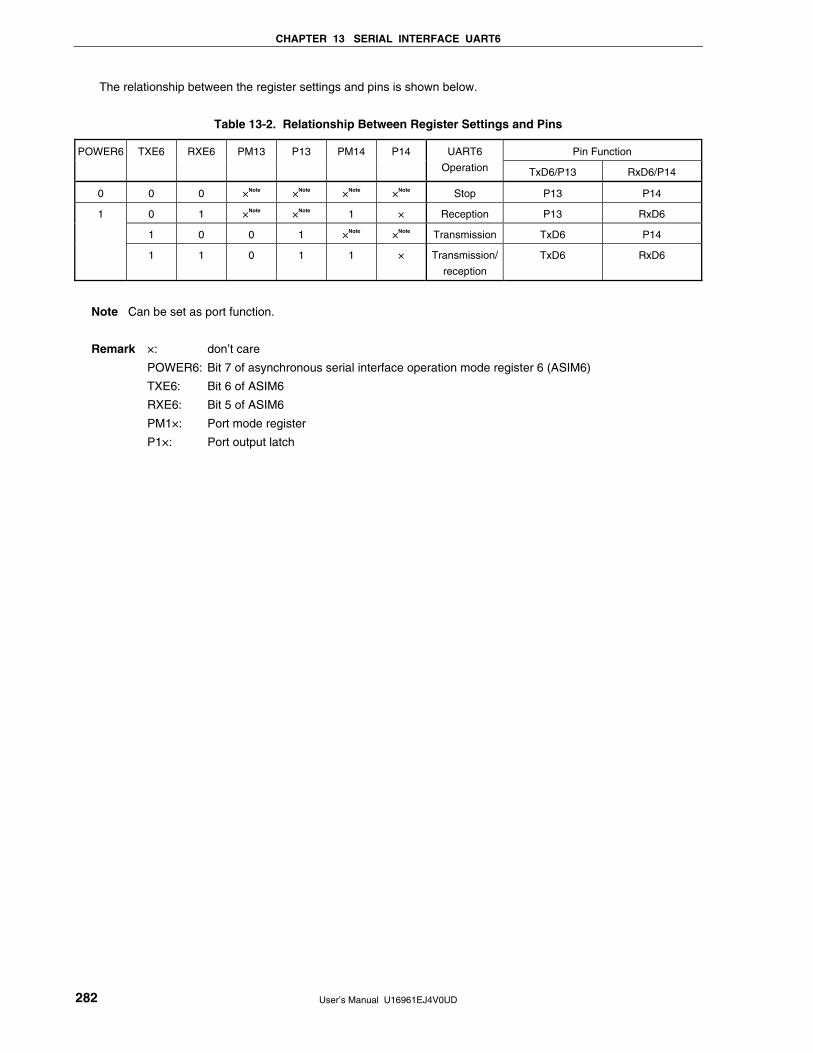
CHAPTER 13 SERIAL INTERFACE UART6
User’s Manual U16961EJ4V0UD 282
The relationship between the register settings and pins is shown below.
Table 13-2. Relationship Between Register Settings and Pins
Pin Function POWER6 TXE6 RXE6 PM13 P13 PM14 P14 UART6
Operation TxD6/P13 RxD6/P14
0 0 0 ×Note ×Note ×Note ×Note Stop P13 P14
0 1 ×Note ×Note 1 × Reception P13 RxD6
1 0 0 1 ×Note ×Note Transmission TxD6 P14
1
1 1 0 1 1 × Transmission/
reception
TxD6 RxD6
Note Can be set as port function.
Remark ×: don’t care
POWER6: Bit 7 of asynchronous serial interface operation mode register 6 (ASIM6)
TXE6: Bit 6 of ASIM6
RXE6: Bit 5 of ASIM6
PM1×: Port mode register
P1×: Port output latch
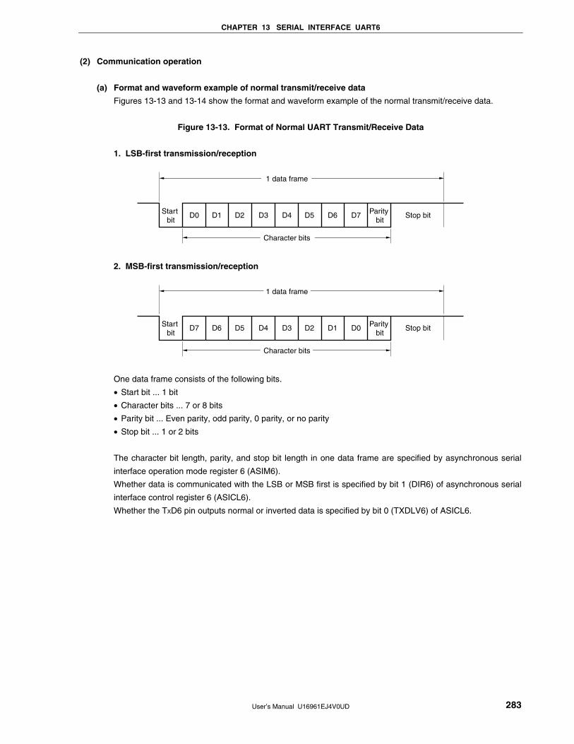
CHAPTER 13 SERIAL INTERFACE UART6
User’s Manual U16961EJ4V0UD 283
(2) Communication operation
(a) Format and waveform example of normal transmit/receive data
Figures 13-13 and 13-14 show the format and waveform example of the normal transmit/receive data.
Figure 13-13. Format of Normal UART Transmit/Receive Data
1. LSB-first transmission/reception
Start bit
Parity bit
D0 D1 D2 D3 D4
1 data frame
Character bits
D5 D6 D7 Stop bit
2. MSB-first transmission/reception
Start bit
Parity bit
D7 D6 D5 D4 D3
1 data frame
Character bits
D2 D1 D0 Stop bit
One data frame consists of the following bits.
• Start bit ... 1 bit
• Character bits ... 7 or 8 bits
• Parity bit ... Even parity, odd parity, 0 parity, or no parity
• Stop bit ... 1 or 2 bits
The character bit length, parity, and stop bit length in one data frame are specified by asynchronous serial
interface operation mode register 6 (ASIM6).
Whether data is communicated with the LSB or MSB first is specified by bit 1 (DIR6) of asynchronous serial
interface control register 6 (ASICL6).
Whether the TXD6 pin outputs normal or inverted data is specified by bit 0 (TXDLV6) of ASICL6.
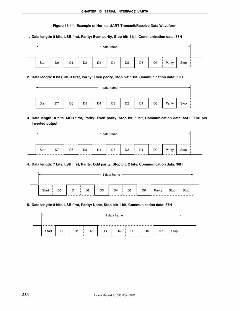
CHAPTER 13 SERIAL INTERFACE UART6
User’s Manual U16961EJ4V0UD 284
Figure 13-14. Example of Normal UART Transmit/Receive Data Waveform
1. Data length: 8 bits, LSB first, Parity: Even parity, Stop bit: 1 bit, Communication data: 55H
1 data frame
Start D0 D1 D2 D3 D4 D5 D6 D7 Parity Stop
2. Data length: 8 bits, MSB first, Parity: Even parity, Stop bit: 1 bit, Communication data: 55H
1 data frame
Start D7 D6 D5 D4 D3 D2 D1 D0 Parity Stop
3. Data length: 8 bits, MSB first, Parity: Even parity, Stop bit: 1 bit, Communication data: 55H, TXD6 pin
inverted output
1 data frame
Start D7 D6 D5 D4 D3 D2 D1 D0 Parity Stop
4. Data length: 7 bits, LSB first, Parity: Odd parity, Stop bit: 2 bits, Communication data: 36H
1 data frame
Start D0 D1 D2 D3 D4 D5 D6 Parity StopStop
5. Data length: 8 bits, LSB first, Parity: None, Stop bit: 1 bit, Communication data: 87H
1 data frame
Start D0 D1 D2 D3 D4 D5 D6 D7 Stop
CHAPTER 13 SERIAL INTERFACE UART6
User’s Manual U16961EJ4V0UD 285
(b) Parity types and operation
The parity bit is used to detect a bit error in communication data. Usually, the same type of parity bit is used
on both the transmission and reception sides. With even parity and odd parity, a 1-bit (odd number) error
can be detected. With zero parity and no parity, an error cannot be detected.
Caution Fix the PS61 and PS60 bits to 0 when UART6 is used in the LIN communication operation.
(i) Even parity
• Transmission
Transmit data, including the parity bit, is controlled so that the number of bits that are “1” is even.
The value of the parity bit is as follows.
If transmit data has an odd number of bits that are “1”: 1
If transmit data has an even number of bits that are “1”: 0
• Reception
The number of bits that are “1” in the receive data, including the parity bit, is counted. If it is odd, a
parity error occurs.
(ii) Odd parity
• Transmission
Unlike even parity, transmit data, including the parity bit, is controlled so that the number of bits that
are “1” is odd.
If transmit data has an odd number of bits that are “1”: 0
If transmit data has an even number of bits that are “1”: 1
• Reception
The number of bits that are “1” in the receive data, including the parity bit, is counted. If it is even, a
parity error occurs.
(iii) 0 parity
The parity bit is cleared to 0 when data is transmitted, regardless of the transmit data.
The parity bit is not detected when the data is received. Therefore, a parity error does not occur
regardless of whether the parity bit is “0” or “1”.
(iv) No parity
No parity bit is appended to the transmit data.
Reception is performed assuming that there is no parity bit when data is received. Because there is no
parity bit, a parity error does not occur.
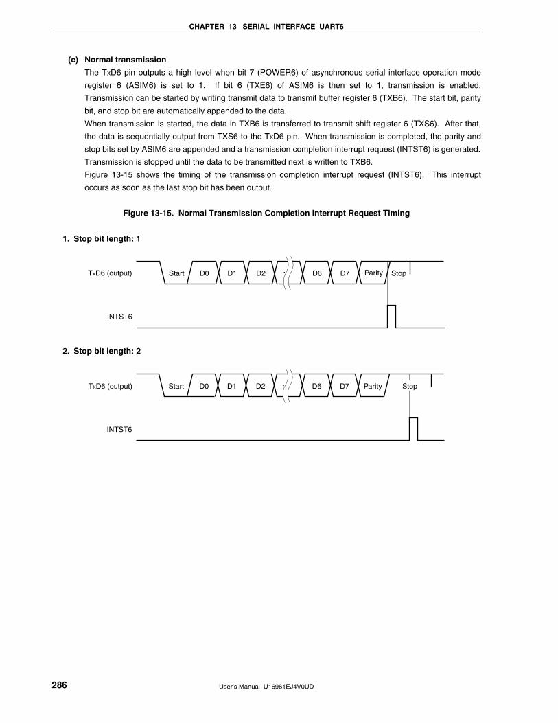
CHAPTER 13 SERIAL INTERFACE UART6
User’s Manual U16961EJ4V0UD 286
(c) Normal transmission
The TXD6 pin outputs a high level when bit 7 (POWER6) of asynchronous serial interface operation mode
register 6 (ASIM6) is set to 1. If bit 6 (TXE6) of ASIM6 is then set to 1, transmission is enabled.
Transmission can be started by writing transmit data to transmit buffer register 6 (TXB6). The start bit, parity
bit, and stop bit are automatically appended to the data.
When transmission is started, the data in TXB6 is transferred to transmit shift register 6 (TXS6). After that,
the data is sequentially output from TXS6 to the TXD6 pin. When transmission is completed, the parity and
stop bits set by ASIM6 are appended and a transmission completion interrupt request (INTST6) is generated.
Transmission is stopped until the data to be transmitted next is written to TXB6.
Figure 13-15 shows the timing of the transmission completion interrupt request (INTST6). This interrupt
occurs as soon as the last stop bit has been output.
Figure 13-15. Normal Transmission Completion Interrupt Request Timing
1. Stop bit length: 1
INTST6
D0Start D1 D2 D6 D7 StopTXD6 (output) Parity
2. Stop bit length: 2
TXD6 (output)
INTST6
D0Start D1 D2 D6 D7 Parity Stop
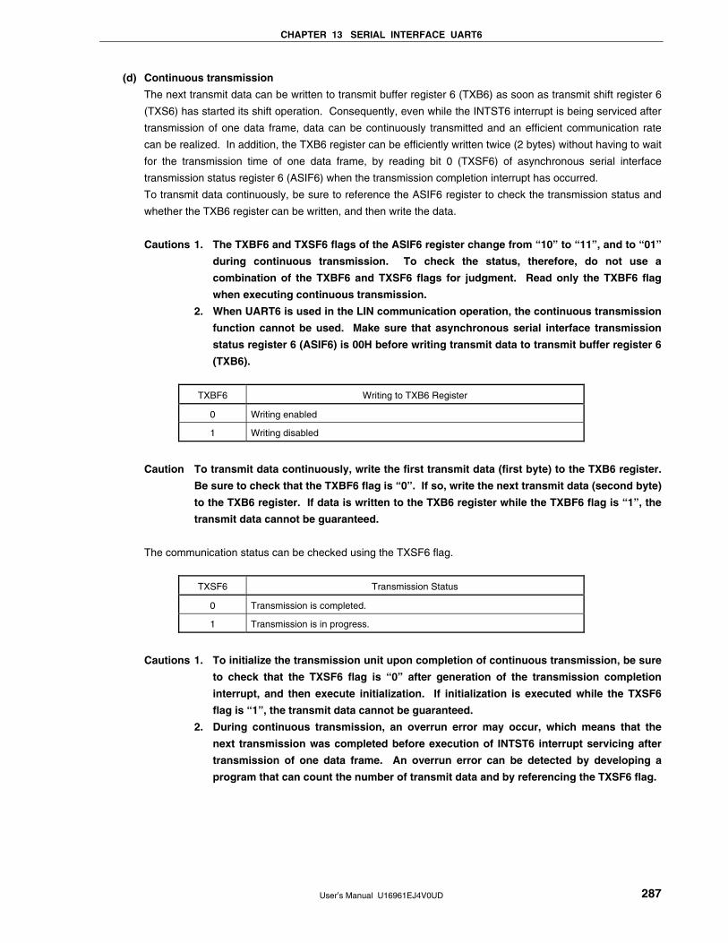
CHAPTER 13 SERIAL INTERFACE UART6
User’s Manual U16961EJ4V0UD 287
(d) Continuous transmission
The next transmit data can be written to transmit buffer register 6 (TXB6) as soon as transmit shift register 6
(TXS6) has started its shift operation. Consequently, even while the INTST6 interrupt is being serviced after
transmission of one data frame, data can be continuously transmitted and an efficient communication rate
can be realized. In addition, the TXB6 register can be efficiently written twice (2 bytes) without having to wait
for the transmission time of one data frame, by reading bit 0 (TXSF6) of asynchronous serial interface
transmission status register 6 (ASIF6) when the transmission completion interrupt has occurred.
To transmit data continuously, be sure to reference the ASIF6 register to check the transmission status and
whether the TXB6 register can be written, and then write the data.
Cautions 1. The TXBF6 and TXSF6 flags of the ASIF6 register change from “10” to “11”, and to “01”
during continuous transmission. To check the status, therefore, do not use a
combination of the TXBF6 and TXSF6 flags for judgment. Read only the TXBF6 flag
when executing continuous transmission.
2. When UART6 is used in the LIN communication operation, the continuous transmission
function cannot be used. Make sure that asynchronous serial interface transmission
status register 6 (ASIF6) is 00H before writing transmit data to transmit buffer register 6
(TXB6).
TXBF6 Writing to TXB6 Register
0 Writing enabled
1 Writing disabled
Caution To transmit data continuously, write the first transmit data (first byte) to the TXB6 register.
Be sure to check that the TXBF6 flag is “0”. If so, write the next transmit data (second byte)
to the TXB6 register. If data is written to the TXB6 register while the TXBF6 flag is “1”, the
transmit data cannot be guaranteed.
The communication status can be checked using the TXSF6 flag.
TXSF6 Transmission Status
0 Transmission is completed.
1 Transmission is in progress.
Cautions 1. To initialize the transmission unit upon completion of continuous transmission, be sure
to check that the TXSF6 flag is “0” after generation of the transmission completion
interrupt, and then execute initialization. If initialization is executed while the TXSF6
flag is “1”, the transmit data cannot be guaranteed.
2. During continuous transmission, an overrun error may occur, which means that the
next transmission was completed before execution of INTST6 interrupt servicing after
transmission of one data frame. An overrun error can be detected by developing a
program that can count the number of transmit data and by referencing the TXSF6 flag.
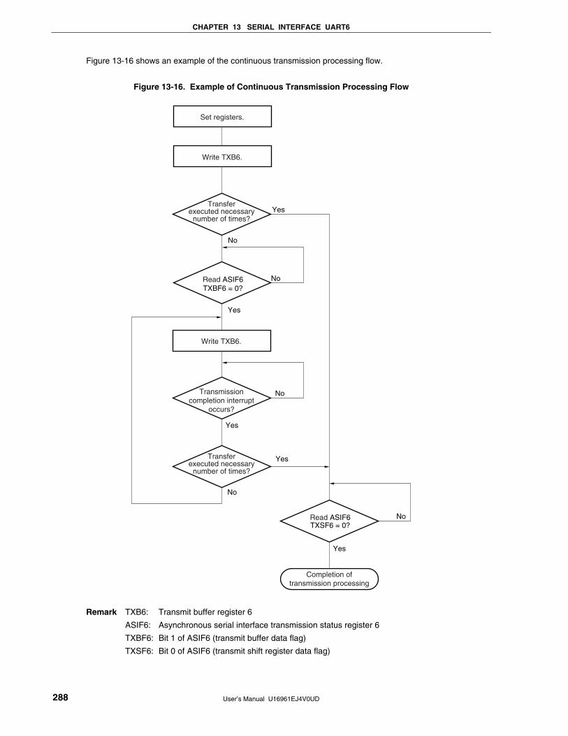
CHAPTER 13 SERIAL INTERFACE UART6
User’s Manual U16961EJ4V0UD 288
Figure 13-16 shows an example of the continuous transmission processing flow.
Figure 13-16. Example of Continuous Transmission Processing Flow
Write TXB6.
Set registers.
Write TXB6.
Transferexecuted necessary
number of times?Yes
Read ASIF6TXBF6 = 0?
No
No
Yes
Transmissioncompletion interrupt
occurs?
Read ASIF6TXSF6 = 0?
No
No
No
Yes
Yes
Yes
YesCompletion oftransmission processing
Transferexecuted necessary
number of times?
Remark TXB6: Transmit buffer register 6
ASIF6: Asynchronous serial interface transmission status register 6
TXBF6: Bit 1 of ASIF6 (transmit buffer data flag)
TXSF6: Bit 0 of ASIF6 (transmit shift register data flag)
CHAPTER 13 SERIAL INTERFACE UART6
User’s Manual U16961EJ4V0UD 289
Figure 13-17 shows the timing of starting continuous transmission, and Figure 13-18 shows the timing of
ending continuous transmission.
Figure 13-17. Timing of Starting Continuous Transmission
TXD6 Start
INTST6
Data (1)
Data (1) Data (2) Data (3)
Data (2)Data (1) Data (3)
FF
FF
Parity Stop Data (2) Parity Stop
TXB6
TXS6
TXBF6
TXSF6
Start Start
Note
Note When ASIF6 is read, there is a period in which TXBF6 and TXSF6 = 1, 1. Therefore, judge whether
writing is enabled using only the TXBF6 bit.
Remark TXD6: TXD6 pin (output)
INTST6: Interrupt request signal
TXB6: Transmit buffer register 6
TXS6: Transmit shift register 6
ASIF6: Asynchronous serial interface transmission status register 6
TXBF6: Bit 1 of ASIF6
TXSF6: Bit 0 of ASIF6
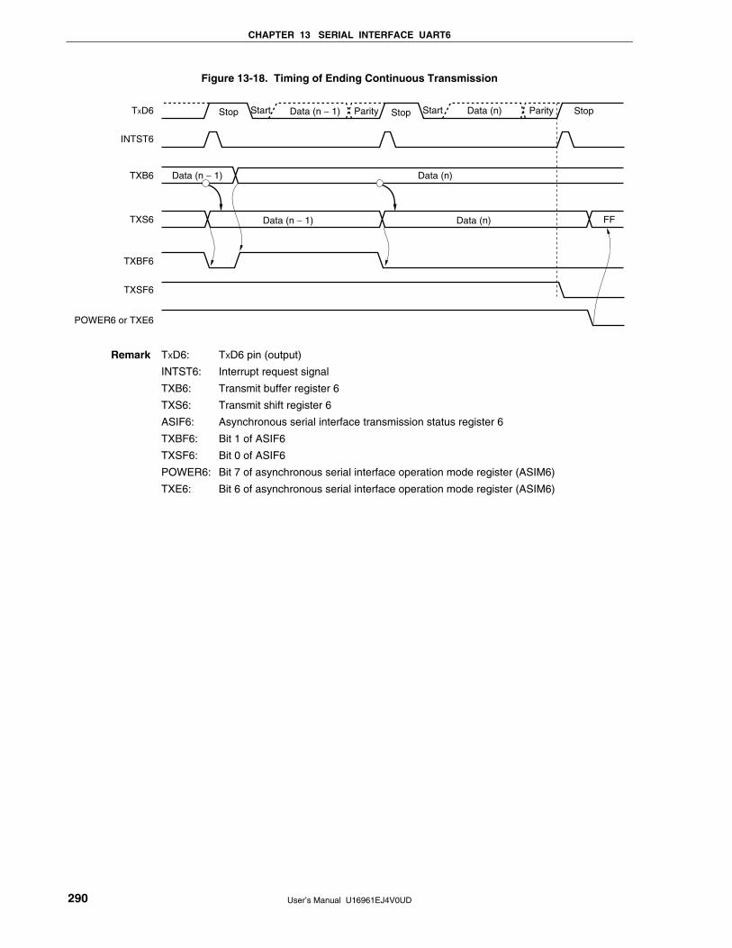
CHAPTER 13 SERIAL INTERFACE UART6
User’s Manual U16961EJ4V0UD 290
Figure 13-18. Timing of Ending Continuous Transmission
TXD6 Start
INTST6
Data (n − 1)
Data (n − 1) Data (n)
Data (n)Data (n − 1) FF
ParityStop Stop Data (n) Parity Stop
TXB6
TXS6
TXBF6
TXSF6
POWER6 or TXE6
Start
Remark TXD6: TXD6 pin (output)
INTST6: Interrupt request signal
TXB6: Transmit buffer register 6
TXS6: Transmit shift register 6
ASIF6: Asynchronous serial interface transmission status register 6
TXBF6: Bit 1 of ASIF6
TXSF6: Bit 0 of ASIF6
POWER6: Bit 7 of asynchronous serial interface operation mode register (ASIM6)
TXE6: Bit 6 of asynchronous serial interface operation mode register (ASIM6)
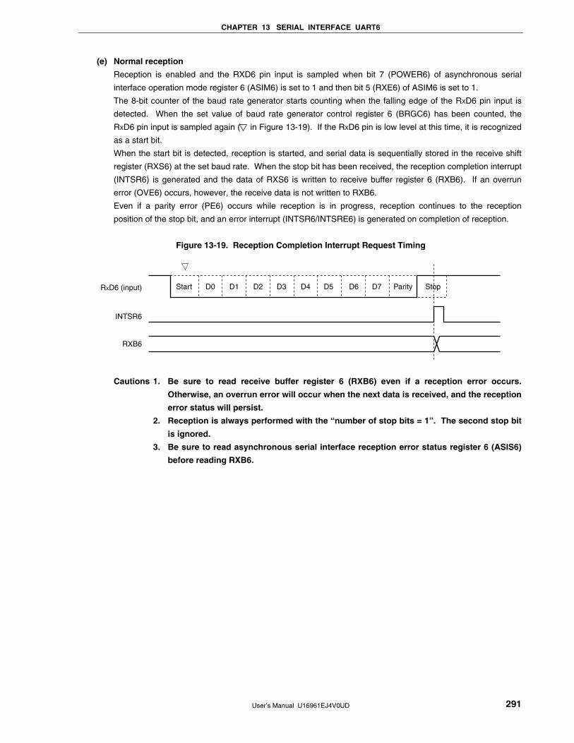
CHAPTER 13 SERIAL INTERFACE UART6
User’s Manual U16961EJ4V0UD 291
(e) Normal reception
Reception is enabled and the RXD6 pin input is sampled when bit 7 (POWER6) of asynchronous serial
interface operation mode register 6 (ASIM6) is set to 1 and then bit 5 (RXE6) of ASIM6 is set to 1.
The 8-bit counter of the baud rate generator starts counting when the falling edge of the RXD6 pin input is
detected. When the set value of baud rate generator control register 6 (BRGC6) has been counted, the
RXD6 pin input is sampled again ( in Figure 13-19). If the RXD6 pin is low level at this time, it is recognized
as a start bit.
When the start bit is detected, reception is started, and serial data is sequentially stored in the receive shift
register (RXS6) at the set baud rate. When the stop bit has been received, the reception completion interrupt
(INTSR6) is generated and the data of RXS6 is written to receive buffer register 6 (RXB6). If an overrun
error (OVE6) occurs, however, the receive data is not written to RXB6.
Even if a parity error (PE6) occurs while reception is in progress, reception continues to the reception
position of the stop bit, and an error interrupt (INTSR6/INTSRE6) is generated on completion of reception.
Figure 13-19. Reception Completion Interrupt Request Timing
RXD6 (input)
INTSR6
Start D0 D1 D2 D3 D4 D5 D6 D7 Parity Stop
RXB6
Cautions 1. Be sure to read receive buffer register 6 (RXB6) even if a reception error occurs.
Otherwise, an overrun error will occur when the next data is received, and the reception
error status will persist.
2. Reception is always performed with the “number of stop bits = 1”. The second stop bit
is ignored.
3. Be sure to read asynchronous serial interface reception error status register 6 (ASIS6)
before reading RXB6.
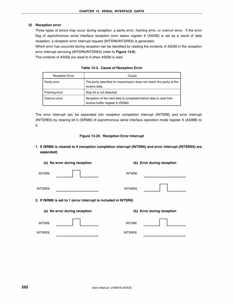
CHAPTER 13 SERIAL INTERFACE UART6
User’s Manual U16961EJ4V0UD 292
(f) Reception error
Three types of errors may occur during reception: a parity error, framing error, or overrun error. If the error
flag of asynchronous serial interface reception error status register 6 (ASIS6) is set as a result of data
reception, a reception error interrupt request (INTSR6/INTSRE6) is generated.
Which error has occurred during reception can be identified by reading the contents of ASIS6 in the reception
error interrupt servicing (INTSR6/INTSRE6) (refer to Figure 13-6).
The contents of ASIS6 are reset to 0 when ASIS6 is read.
Table 13-3. Cause of Reception Error
Reception Error Cause
Parity error The parity specified for transmission does not match the parity of the
receive data.
Framing error Stop bit is not detected.
Overrun error Reception of the next data is completed before data is read from
receive buffer register 6 (RXB6).
The error interrupt can be separated into reception completion interrupt (INTSR6) and error interrupt
(INTSRE6) by clearing bit 0 (ISRM6) of asynchronous serial interface operation mode register 6 (ASIM6) to
0.
Figure 13-20. Reception Error Interrupt
1. If ISRM6 is cleared to 0 (reception completion interrupt (INTSR6) and error interrupt (INTSRE6) are
separated)
(a) No error during reception (b) Error during reception
INTSR6
INTSRE6
INTSR6
INTSRE6
2. If ISRM6 is set to 1 (error interrupt is included in INTSR6)
(a) No error during reception (b) Error during reception
INTSRE6
INTSR6
INTSRE6
INTSR6
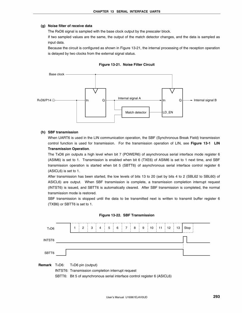
CHAPTER 13 SERIAL INTERFACE UART6
User’s Manual U16961EJ4V0UD 293
(g) Noise filter of receive data
The RxD6 signal is sampled with the base clock output by the prescaler block.
If two sampled values are the same, the output of the match detector changes, and the data is sampled as
input data.
Because the circuit is configured as shown in Figure 13-21, the internal processing of the reception operation
is delayed by two clocks from the external signal status.
Figure 13-21. Noise Filter Circuit
Internal signal BInternal signal A
Match detector
In
Base clock
RXD6/P14 Q In
LD_EN
Q
(h) SBF transmission
When UART6 is used in the LIN communication operation, the SBF (Synchronous Break Field) transmission
control function is used for transmission. For the transmission operation of LIN, see Figure 13-1 LIN
Transmission Operation.
The TxD6 pin outputs a high level when bit 7 (POWER6) of asynchronous serial interface mode register 6
(ASIM6) is set to 1. Transmission is enabled when bit 6 (TXE6) of ASIM6 is set to 1 next time, and SBF
transmission operation is started when bit 5 (SBTT6) of asynchronous serial interface control register 6
(ASICL6) is set to 1.
After transmission has been started, the low levels of bits 13 to 20 (set by bits 4 to 2 (SBL62 to SBL60) of
ASICL6) are output. When SBF transmission is complete, a transmission completion interrupt request
(INTST6) is issued, and SBTT6 is automatically cleared. After SBF transmission is completed, the normal
transmission mode is restored.
SBF transmission is stopped until the data to be transmitted next is written to transmit buffer register 6
(TXB6) or SBTT6 is set to 1.
Figure 13-22. SBF Transmission
TXD6
INTST6
SBTT6
1 2 3 4 5 6 7 8 9 10 11 12 13 Stop
Remark TXD6: TXD6 pin (output)
INTST6: Transmission completion interrupt request
SBTT6: Bit 5 of asynchronous serial interface control register 6 (ASICL6)
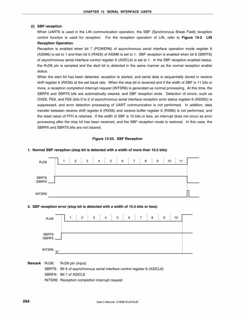
CHAPTER 13 SERIAL INTERFACE UART6
User’s Manual U16961EJ4V0UD 294
(i) SBF reception
When UART6 is used in the LIN communication operation, the SBF (Synchronous Break Field) reception
control function is used for reception. For the reception operation of LIN, refer to Figure 13-2 LIN
Reception Operation.
Reception is enabled when bit 7 (POWER6) of asynchronous serial interface operation mode register 6
(ASIM6) is set to 1 and then bit 5 (RXE6) of ASIM6 is set to 1. SBF reception is enabled when bit 6 (SBRT6)
of asynchronous serial interface control register 6 (ASICL6) is set to 1. In the SBF reception enabled status,
the RXD6 pin is sampled and the start bit is detected in the same manner as the normal reception enable
status.
When the start bit has been detected, reception is started, and serial data is sequentially stored in receive
shift register 6 (RXS6) at the set baud rate. When the stop bit is received and if the width of SBF is 11 bits or
more, a reception completion interrupt request (INTSR6) is generated as normal processing. At this time, the
SBRF6 and SBRT6 bits are automatically cleared, and SBF reception ends. Detection of errors, such as
OVE6, PE6, and FE6 (bits 0 to 2 of asynchronous serial interface reception error status register 6 (ASIS6)) is
suppressed, and error detection processing of UART communication is not performed. In addition, data
transfer between receive shift register 6 (RXS6) and receive buffer register 6 (RXB6) is not performed, and
the reset value of FFH is retained. If the width of SBF is 10 bits or less, an interrupt does not occur as error
processing after the stop bit has been received, and the SBF reception mode is restored. In this case, the
SBRF6 and SBRT6 bits are not cleared.
Figure 13-23. SBF Reception
1. Normal SBF reception (stop bit is detected with a width of more than 10.5 bits)
RXD6
SBRT6/SBRF6
INTSR6
1 2 3 4 5 6 7 8 9 10 11
2. SBF reception error (stop bit is detected with a width of 10.5 bits or less)
RXD6
SBRT6/SBRF6
INTSR6
1 2 3 4 5 6 7 8 9 10
“0”
Remark RXD6: RXD6 pin (input)
SBRT6: Bit 6 of asynchronous serial interface control register 6 (ASICL6)
SBRF6: Bit 7 of ASICL6
INTSR6: Reception completion interrupt request
CHAPTER 13 SERIAL INTERFACE UART6
User’s Manual U16961EJ4V0UD 295
13.4.3 Dedicated baud rate generator
The dedicated baud rate generator consists of a source clock selector and an 8-bit programmable counter, and
generates a serial clock for transmission/reception of UART6.
Separate 8-bit counters are provided for transmission and reception.
(1) Configuration of baud rate generator
• Base clock
The clock selected by bits 3 to 0 (TPS63 to TPS60) of clock selection register 6 (CKSR6) is supplied to
each module when bit 7 (POWER6) of asynchronous serial interface operation mode register 6 (ASIM6) is
1. This clock is called the base clock and its frequency is called fXCLK6. The base clock is fixed to low level
when POWER6 = 0.
• Transmission counter
This counter stops operation, cleared to 0, when bit 7 (POWER6) or bit 6 (TXE6) of asynchronous serial
interface operation mode register 6 (ASIM6) is 0.
It starts counting when POWER6 = 1 and TXE6 = 1.
The counter is cleared to 0 when the first data transmitted is written to transmit buffer register 6 (TXB6).
If data are continuously transmitted, the counter is cleared to 0 again when one frame of data has been
completely transmitted. If there is no data to be transmitted next, the counter is not cleared to 0 and continues
counting until POWER6 or TXE6 is cleared to 0.
• Reception counter
This counter stops operation, cleared to 0, when bit 7 (POWER6) or bit 5 (RXE6) of asynchronous serial
interface operation mode register 6 (ASIM6) is 0.
It starts counting when the start bit has been detected.
The counter stops operation after one frame has been received, until the next start bit is detected.
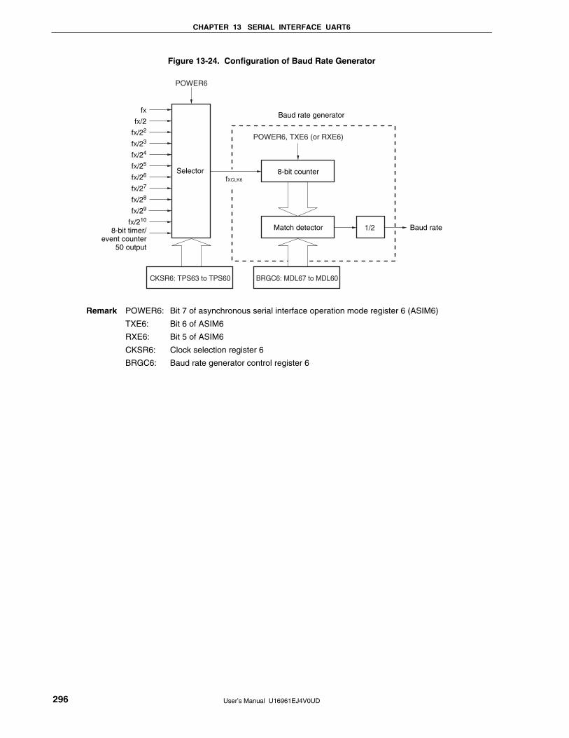
CHAPTER 13 SERIAL INTERFACE UART6
User’s Manual U16961EJ4V0UD 296
Figure 13-24. Configuration of Baud Rate Generator
Selector
POWER6
8-bit counter
Match detector Baud rate
Baud rate generator
BRGC6: MDL67 to MDL60
1/2
POWER6, TXE6 (or RXE6)
CKSR6: TPS63 to TPS60
fX
fX/2
fX/22
fX/23
fX/24
fX/25
fX/26
fX/27
fX/28
fX/29
fX/210
8-bit timer/event counter
50 output
fXCLK6
Remark POWER6: Bit 7 of asynchronous serial interface operation mode register 6 (ASIM6)
TXE6: Bit 6 of ASIM6
RXE6: Bit 5 of ASIM6
CKSR6: Clock selection register 6
BRGC6: Baud rate generator control register 6
CHAPTER 13 SERIAL INTERFACE UART6
User’s Manual U16961EJ4V0UD 297
(2) Generation of serial clock
A serial clock can be generated by using clock selection register 6 (CKSR6) and baud rate generator control
register 6 (BRGC6).
Select the clock to be input to the 8-bit counter by using bits 3 to 0 (TPS63 to TPS60) of CKSR6.
Bits 7 to 0 (MDL67 to MDL60) of BRGC6 can be used to select the division value of the 8-bit counter.
(a) Baud rate
The baud rate can be calculated by the following expression.
• Baud rate = [bps]
Remark fXCLK6: Frequency of base clock selected by TPS63 to TPS60 bits of CKSR6 register
k: Value set by MDL67 to MDL60 bits of BRGC6 register (k = 8, 9, 10, ..., 255)
(b) Error of baud rate
The baud rate error can be calculated by the following expression.
• Error (%) = − 1 × 100 [%]
Cautions 1. Keep the baud rate error during transmission to within the permissible error range at
the reception destination.
2. Make sure that the baud rate error during reception satisfies the range shown in (4)
Permissible baud rate range during reception.
Example: Frequency of base clock = 10 MHz = 10,000,000 Hz
Set value of MDL67 to MDL60 bits of BRGC6 register = 00100001B (k = 33)
Target baud rate = 153600 bps
Baud rate = 10 M/(2 × 33)
= 10000000/(2 × 33) = 151,515 [bps]
Error = (151515/153600 − 1) × 100
= −1.357 [%]
Actual baud rate (baud rate with error)
Desired baud rate (correct baud rate)
fXCLK6
2 × k
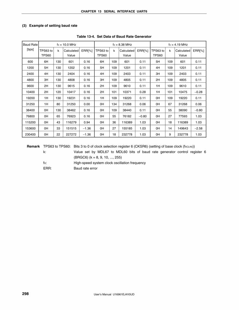
CHAPTER 13 SERIAL INTERFACE UART6
User’s Manual U16961EJ4V0UD 298
(3) Example of setting baud rate
Table 13-4. Set Data of Baud Rate Generator
fX = 10.0 MHz fX = 8.38 MHz fX = 4.19 MHz Baud Rate
[bps] TPS63 to
TPS60
k Calculated
Value
ERR[%] TPS63 to
TPS60
k Calculated
Value
ERR[%] TPS63 to
TPS60
k Calculated
Value
ERR[%]
600 6H 130 601 0.16 6H 109 601 0.11 5H 109 601 0.11
1200 5H 130 1202 0.16 5H 109 1201 0.11 4H 109 1201 0.11
2400 4H 130 2404 0.16 4H 109 2403 0.11 3H 109 2403 0.11
4800 3H 130 4808 0.16 3H 109 4805 0.11 2H 109 4805 0.11
9600 2H 130 9615 0.16 2H 109 9610 0.11 1H 109 9610 0.11
10400 2H 120 10417 0.16 2H 101 10371 0.28 1H 101 10475 −0.28
19200 1H 130 19231 0.16 1H 109 19220 0.11 0H 109 19220 0.11
31250 1H 80 31250 0.00 0H 134 31268 0.06 0H 67 31268 0.06
38400 0H 130 38462 0.16 0H 109 38440 0.11 0H 55 38090 −0.80
76800 0H 65 76923 0.16 0H 55 76182 −0.80 0H 27 77593 1.03
115200 0H 43 116279 0.94 0H 36 116389 1.03 0H 18 116389 1.03
153600 0H 33 151515 −1.36 0H 27 155185 1.03 0H 14 149643 −2.58
230400 0H 22 227272 −1.36 0H 18 232778 1.03 0H 9 232778 1.03
Remark TPS63 to TPS60: Bits 3 to 0 of clock selection register 6 (CKSR6) (setting of base clock (fXCLK6))
k: Value set by MDL67 to MDL60 bits of baud rate generator control register 6
(BRGC6) (k = 8, 9, 10, ..., 255)
fX: High-speed system clock oscillation frequency
ERR: Baud rate error
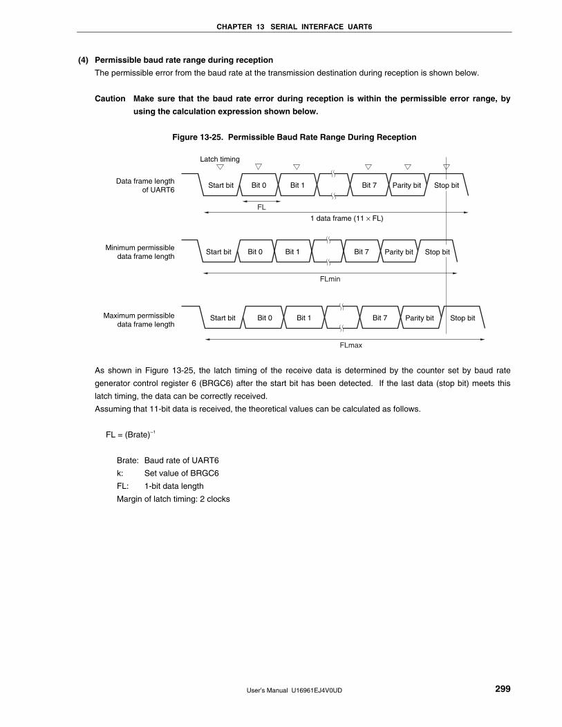
CHAPTER 13 SERIAL INTERFACE UART6
User’s Manual U16961EJ4V0UD 299
(4) Permissible baud rate range during reception
The permissible error from the baud rate at the transmission destination during reception is shown below.
Caution Make sure that the baud rate error during reception is within the permissible error range, by
using the calculation expression shown below.
Figure 13-25. Permissible Baud Rate Range During Reception
FL
1 data frame (11 × FL)
FLmin
FLmax
Data frame lengthof UART6
Start bit Bit 0 Bit 1 Bit 7 Parity bit
Minimum permissibledata frame length
Maximum permissibledata frame length
Stop bit
Start bit Bit 0 Bit 1 Bit 7 Parity bit
Latch timing
Stop bit
Start bit Bit 0 Bit 1 Bit 7 Parity bit Stop bit
As shown in Figure 13-25, the latch timing of the receive data is determined by the counter set by baud rate
generator control register 6 (BRGC6) after the start bit has been detected. If the last data (stop bit) meets this
latch timing, the data can be correctly received.
Assuming that 11-bit data is received, the theoretical values can be calculated as follows.
FL = (Brate)−1
Brate: Baud rate of UART6
k: Set value of BRGC6
FL: 1-bit data length
Margin of latch timing: 2 clocks
CHAPTER 13 SERIAL INTERFACE UART6
User’s Manual U16961EJ4V0UD 300
Minimum permissible data frame length: FLmin = 11 × FL − × FL = FL
Therefore, the maximum receivable baud rate at the transmission destination is as follows.
BRmax = (FLmin/11)−1 = Brate
Similarly, the maximum permissible data frame length can be calculated as follows.
10 k + 2 21k − 2
11 2 × k 2 × k
FLmax = FL × 11
Therefore, the minimum receivable baud rate at the transmission destination is as follows.
BRmin = (FLmax/11)−1 = Brate
The permissible baud rate error between UART6 and the transmission destination can be calculated from the
above minimum and maximum baud rate expressions, as follows.
Table 13-5. Maximum/Minimum Permissible Baud Rate Error
Division Ratio (k) Maximum Permissible Baud Rate Error Minimum Permissible Baud Rate Error
8 +3.53% −3.61%
20 +4.26% −4.31%
50 +4.56% −4.58%
100 +4.66% −4.67%
255 +4.72% −4.73%
Remarks 1. The permissible error of reception depends on the number of bits in one frame, input clock
frequency, and division ratio (k). The higher the input clock frequency and the higher the division
ratio (k), the higher the permissible error.
2. k: Set value of BRGC6
k − 2
2k
21k + 2
2k
22k
21k + 2
× FLmax = 11 × FL − × FL = FL
21k – 2
20k
20k
21k − 2
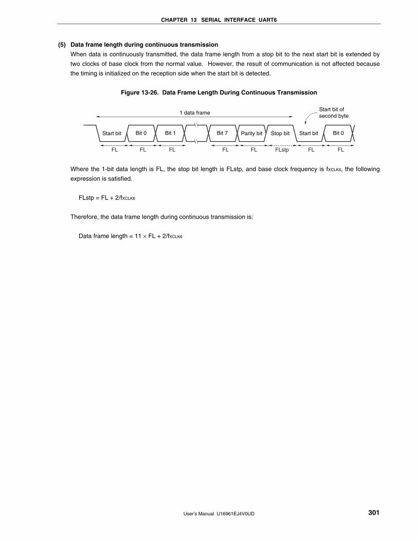
CHAPTER 13 SERIAL INTERFACE UART6
User’s Manual U16961EJ4V0UD 301
(5) Data frame length during continuous transmission
When data is continuously transmitted, the data frame length from a stop bit to the next start bit is extended by
two clocks of base clock from the normal value. However, the result of communication is not affected because
the timing is initialized on the reception side when the start bit is detected.
Figure 13-26. Data Frame Length During Continuous Transmission
Start bit Bit 0 Bit 1 Bit 7 Parity bit Stop bit
FL
1 data frame
FL FL FL FL FLFLFLstp
Start bit of second byte
Start bit Bit 0
Where the 1-bit data length is FL, the stop bit length is FLstp, and base clock frequency is fXCLK6, the following
expression is satisfied.
FLstp = FL + 2/fXCLK6
Therefore, the data frame length during continuous transmission is:
Data frame length = 11 × FL + 2/fXCLK6
User’s Manual U16961EJ4V0UD 302
CHAPTER 14 SERIAL INTERFACE CSI10
14.1 Functions of Serial Interface CSI10
Serial interface CSI10 has the following two modes.
• Operation stop mode
• 3-wire serial I/O mode
(1) Operation stop mode
This mode is used when serial communication is not performed and can enable a reduction in the power
consumption.
For details, see 14.4.1 Operation stop mode.
(2) 3-wire serial I/O mode (MSB/LSB-first selectable)
This mode is used to communicate 8-bit data using three lines: a serial clock line (SCK10) and two serial data
lines (SI10 and SO10).
The processing time of data communication can be shortened in the 3-wire serial I/O mode because transmission
and reception can be simultaneously executed.
In addition, whether 8-bit data is communicated with the MSB or LSB first can be specified, so this interface can
be connected to any device.
The 3-wire serial I/O mode is used for connecting peripheral ICs and display controllers with a clocked serial
interface.
For details, see 14.4.2 3-wire serial I/O mode.
14.2 Configuration of Serial Interface CSI10
Serial interface CSI10 includes the following hardware.
Table 14-1. Configuration of Serial Interface CSI10
Item Configuration
Registers Transmit buffer register 10 (SOTB10)
Serial I/O shift register 10 (SIO10)
Control registers Serial operation mode register 10 (CSIM10)
Serial clock selection register 10 (CSIC10)
Port mode register 1 (PM1)
Port register 1 (P1)
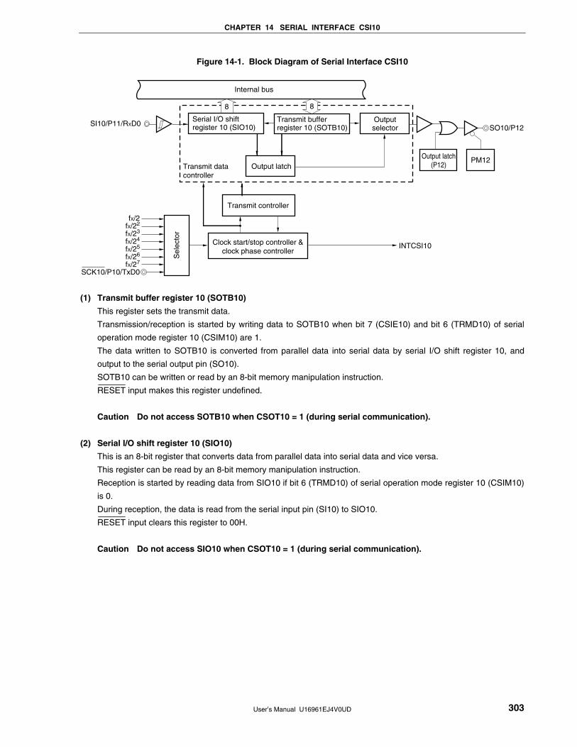
CHAPTER 14 SERIAL INTERFACE CSI10
User’s Manual U16961EJ4V0UD 303
Figure 14-1. Block Diagram of Serial Interface CSI10
Internal bus
SI10/P11/RXD0
INTCSI10
fX/2fX/22
fX/23
fX/24
fX/25
fX/26
fX/27
SCK10/P10/TxD0
Transmit bufferregister 10 (SOTB10)
Transmit controller
Clock start/stop controller &clock phase controller
Serial I/O shiftregister 10 (SIO10)
Outputselector SO10/P12
Output latch
8
Transmit datacontroller
8
Output latch(P12)
PM12
Sel
ecto
r
(1) Transmit buffer register 10 (SOTB10)
This register sets the transmit data.
Transmission/reception is started by writing data to SOTB10 when bit 7 (CSIE10) and bit 6 (TRMD10) of serial
operation mode register 10 (CSIM10) are 1.
The data written to SOTB10 is converted from parallel data into serial data by serial I/O shift register 10, and
output to the serial output pin (SO10).
SOTB10 can be written or read by an 8-bit memory manipulation instruction.
RESET input makes this register undefined.
Caution Do not access SOTB10 when CSOT10 = 1 (during serial communication).
(2) Serial I/O shift register 10 (SIO10)
This is an 8-bit register that converts data from parallel data into serial data and vice versa.
This register can be read by an 8-bit memory manipulation instruction.
Reception is started by reading data from SIO10 if bit 6 (TRMD10) of serial operation mode register 10 (CSIM10)
is 0.
During reception, the data is read from the serial input pin (SI10) to SIO10.
RESET input clears this register to 00H.
Caution Do not access SIO10 when CSOT10 = 1 (during serial communication).
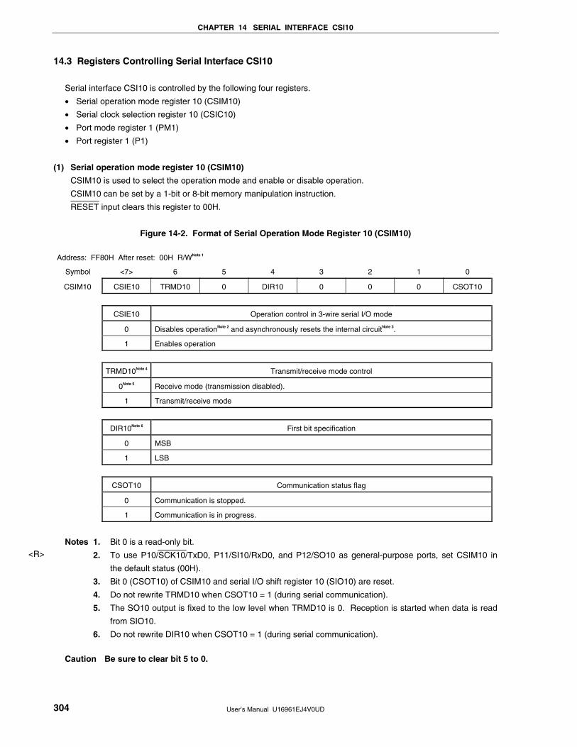
CHAPTER 14 SERIAL INTERFACE CSI10
User’s Manual U16961EJ4V0UD 304
14.3 Registers Controlling Serial Interface CSI10
Serial interface CSI10 is controlled by the following four registers.
• Serial operation mode register 10 (CSIM10)
• Serial clock selection register 10 (CSIC10)
• Port mode register 1 (PM1)
• Port register 1 (P1)
(1) Serial operation mode register 10 (CSIM10)
CSIM10 is used to select the operation mode and enable or disable operation.
CSIM10 can be set by a 1-bit or 8-bit memory manipulation instruction.
RESET input clears this register to 00H.
Figure 14-2. Format of Serial Operation Mode Register 10 (CSIM10)
Address: FF80H After reset: 00H R/WNote 1
Symbol <7> 6 5 4 3 2 1 0
CSIM10 CSIE10 TRMD10 0 DIR10 0 0 0 CSOT10
CSIE10 Operation control in 3-wire serial I/O mode
0 Disables operationNote 2 and asynchronously resets the internal circuitNote 3.
1 Enables operation
TRMD10Note 4 Transmit/receive mode control
0Note 5 Receive mode (transmission disabled).
1 Transmit/receive mode
DIR10Note 6 First bit specification
0 MSB
1 LSB
CSOT10 Communication status flag
0 Communication is stopped.
1 Communication is in progress.
Notes 1. Bit 0 is a read-only bit.
2. To use P10/SCK10/TxD0, P11/SI10/RxD0, and P12/SO10 as general-purpose ports, set CSIM10 in
the default status (00H).
3. Bit 0 (CSOT10) of CSIM10 and serial I/O shift register 10 (SIO10) are reset.
4. Do not rewrite TRMD10 when CSOT10 = 1 (during serial communication).
5. The SO10 output is fixed to the low level when TRMD10 is 0. Reception is started when data is read
from SIO10.
6. Do not rewrite DIR10 when CSOT10 = 1 (during serial communication).
Caution Be sure to clear bit 5 to 0.
<R>
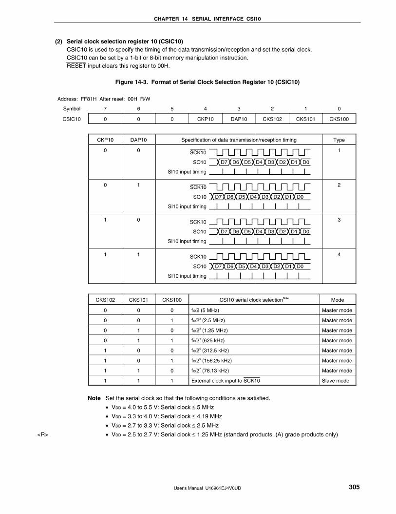
CHAPTER 14 SERIAL INTERFACE CSI10
User’s Manual U16961EJ4V0UD 305
(2) Serial clock selection register 10 (CSIC10) CSIC10 is used to specify the timing of the data transmission/reception and set the serial clock. CSIC10 can be set by a 1-bit or 8-bit memory manipulation instruction. RESET input clears this register to 00H.
Figure 14-3. Format of Serial Clock Selection Register 10 (CSIC10)
Address: FF81H After reset: 00H R/W
Symbol 7 6 5 4 3 2 1 0
CSIC10 0 0 0 CKP10 DAP10 CKS102 CKS101 CKS100
CKP10 DAP10 Specification of data transmission/reception timing Type
0 0
D7 D6 D5 D4 D3 D2 D1 D0
SCK10
SO10
SI10 input timing
1
0 1
D7 D6 D5 D4 D3 D2 D1 D0
SCK10
SO10
SI10 input timing
2
1 0
D7 D6 D5 D4 D3 D2 D1 D0
SCK10
SO10
SI10 input timing
3
1 1
D7 D6 D5 D4 D3 D2 D1 D0
SCK10
SO10
SI10 input timing
4
CKS102 CKS101 CKS100 CSI10 serial clock selectionNote Mode
0 0 0 fX/2 (5 MHz) Master mode
0 0 1 fX/22 (2.5 MHz) Master mode
0 1 0 fX/23 (1.25 MHz) Master mode
0 1 1 fX/24 (625 kHz) Master mode
1 0 0 fX/25 (312.5 kHz) Master mode
1 0 1 fX/26 (156.25 kHz) Master mode
1 1 0 fX/27 (78.13 kHz) Master mode
1 1 1 External clock input to SCK10 Slave mode
Note Set the serial clock so that the following conditions are satisfied.
• VDD = 4.0 to 5.5 V: Serial clock ≤ 5 MHz
• VDD = 3.3 to 4.0 V: Serial clock ≤ 4.19 MHz
• VDD = 2.7 to 3.3 V: Serial clock ≤ 2.5 MHz
• VDD = 2.5 to 2.7 V: Serial clock ≤ 1.25 MHz (standard products, (A) grade products only)
<R>
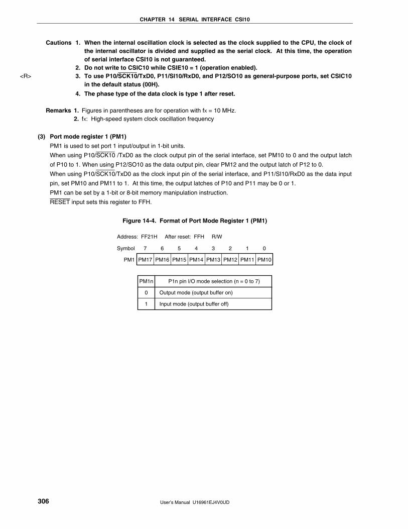
CHAPTER 14 SERIAL INTERFACE CSI10
User’s Manual U16961EJ4V0UD 306
Cautions 1. When the internal oscillation clock is selected as the clock supplied to the CPU, the clock of the internal oscillator is divided and supplied as the serial clock. At this time, the operation of serial interface CSI10 is not guaranteed.
2. Do not write to CSIC10 while CSIE10 = 1 (operation enabled). 3. To use P10/SCK10/TxD0, P11/SI10/RxD0, and P12/SO10 as general-purpose ports, set CSIC10
in the default status (00H).
4. The phase type of the data clock is type 1 after reset.
Remarks 1. Figures in parentheses are for operation with fX = 10 MHz. 2. fX: High-speed system clock oscillation frequency
(3) Port mode register 1 (PM1)
PM1 is used to set port 1 input/output in 1-bit units.
When using P10/SCK10 /TxD0 as the clock output pin of the serial interface, set PM10 to 0 and the output latch
of P10 to 1. When using P12/SO10 as the data output pin, clear PM12 and the output latch of P12 to 0.
When using P10/SCK10/TxD0 as the clock input pin of the serial interface, and P11/SI10/RxD0 as the data input
pin, set PM10 and PM11 to 1. At this time, the output latches of P10 and P11 may be 0 or 1.
PM1 can be set by a 1-bit or 8-bit memory manipulation instruction.
RESET input sets this register to FFH.
Figure 14-4. Format of Port Mode Register 1 (PM1)
7
PM17
6
PM16
5
PM15
4
PM14
3
PM13
2
PM12
1
PM11
0
PM10
Symbol
PM1
Address: FF21H After reset: FFH R/W
PM1n
0
1
P1n pin I/O mode selection (n = 0 to 7)
Output mode (output buffer on)
Input mode (output buffer off)
<R>
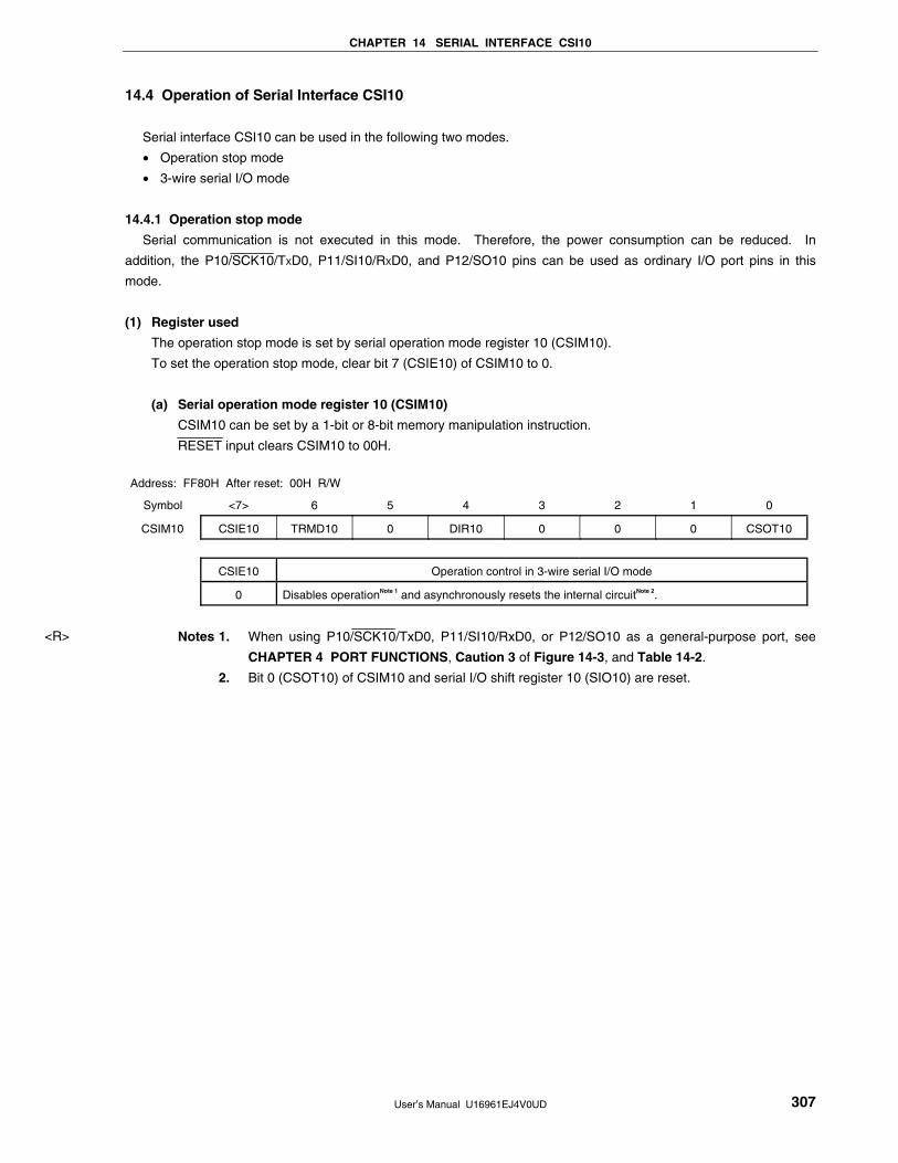
CHAPTER 14 SERIAL INTERFACE CSI10
User’s Manual U16961EJ4V0UD 307
14.4 Operation of Serial Interface CSI10
Serial interface CSI10 can be used in the following two modes.
• Operation stop mode
• 3-wire serial I/O mode
14.4.1 Operation stop mode
Serial communication is not executed in this mode. Therefore, the power consumption can be reduced. In
addition, the P10/SCK10/TXD0, P11/SI10/RXD0, and P12/SO10 pins can be used as ordinary I/O port pins in this
mode.
(1) Register used
The operation stop mode is set by serial operation mode register 10 (CSIM10).
To set the operation stop mode, clear bit 7 (CSIE10) of CSIM10 to 0.
(a) Serial operation mode register 10 (CSIM10)
CSIM10 can be set by a 1-bit or 8-bit memory manipulation instruction.
RESET input clears CSIM10 to 00H.
Address: FF80H After reset: 00H R/W
Symbol <7> 6 5 4 3 2 1 0
CSIM10 CSIE10 TRMD10 0 DIR10 0 0 0 CSOT10
CSIE10 Operation control in 3-wire serial I/O mode
0 Disables operationNote 1 and asynchronously resets the internal circuitNote 2.
Notes 1. When using P10/SCK10/TxD0, P11/SI10/RxD0, or P12/SO10 as a general-purpose port, see
CHAPTER 4 PORT FUNCTIONS, Caution 3 of Figure 14-3, and Table 14-2.
2. Bit 0 (CSOT10) of CSIM10 and serial I/O shift register 10 (SIO10) are reset.
<R>
CHAPTER 14 SERIAL INTERFACE CSI10
User’s Manual U16961EJ4V0UD 308
14.4.2 3-wire serial I/O mode
The 3-wire serial I/O mode is used for connecting peripheral ICs and display controllers that have a clocked serial
interface.
In this mode, communication is executed by using three lines: the serial clock (SCK10), serial output (SO10), and
serial input (SI10) lines.
(1) Registers used
• Serial operation mode register 10 (CSIM10)
• Serial clock selection register 10 (CSIC10)
• Port mode register 1 (PM1)
• Port register 1 (P1)
The basic procedure of setting an operation in the 3-wire serial I/O mode is as follows.
<1> Set the CSIC10 register (see Figure 14-3).
<2> Set bits 0, 4, and 6 (CSOT10, DIR10, and TRMD10) of the CSIM10 register (see Figure 14-2).
<3> Set bit 7 (CSIE10) of the CSIM10 register to 1. → Transmission/reception is enabled.
<4> Write data to transmit buffer register 10 (SOTB10). → Data transmission/reception is started.
Read data from serial I/O shift register 10 (SIO10). → Data reception is started.
Caution Take relationship with the other party of communication when setting the port mode
register and port register.
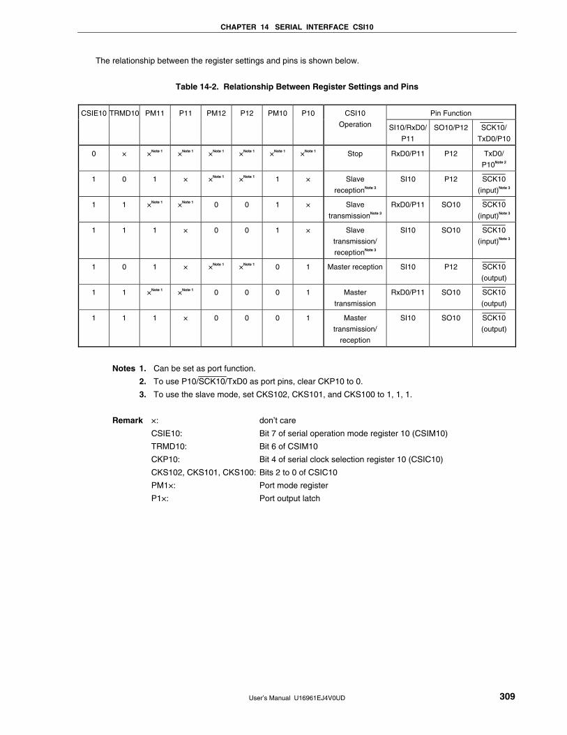
CHAPTER 14 SERIAL INTERFACE CSI10
User’s Manual U16961EJ4V0UD 309
The relationship between the register settings and pins is shown below.
Table 14-2. Relationship Between Register Settings and Pins
Pin Function CSIE10 TRMD10 PM11 P11 PM12 P12 PM10 P10 CSI10
Operation SI10/RxD0/
P11
SO10/P12 SCK10/
TxD0/P10
0 × ×Note 1 ×Note 1 ×Note 1 ×Note 1 ×Note 1 ×Note 1 Stop RxD0/P11 P12 TxD0/
P10Note 2
1 0 1 × ×Note 1 ×Note 1 1 × Slave
receptionNote 3
SI10 P12 SCK10
(input)Note 3
1 1 ×Note 1 ×Note 1 0 0 1 × Slave
transmissionNote 3
RxD0/P11 SO10 SCK10
(input)Note 3
1 1 1 × 0 0 1 × Slave
transmission/
receptionNote 3
SI10 SO10 SCK10
(input)Note 3
1 0 1 × ×Note 1 ×Note 1 0 1 Master reception SI10 P12 SCK10
(output)
1 1 ×Note 1 ×Note 1 0 0 0 1 Master
transmission
RxD0/P11 SO10 SCK10
(output)
1 1 1 × 0 0 0 1 Master
transmission/
reception
SI10 SO10 SCK10
(output)
Notes 1. Can be set as port function.
2. To use P10/SCK10/TxD0 as port pins, clear CKP10 to 0.
3. To use the slave mode, set CKS102, CKS101, and CKS100 to 1, 1, 1.
Remark ×: don’t care
CSIE10: Bit 7 of serial operation mode register 10 (CSIM10)
TRMD10: Bit 6 of CSIM10
CKP10: Bit 4 of serial clock selection register 10 (CSIC10)
CKS102, CKS101, CKS100: Bits 2 to 0 of CSIC10
PM1×: Port mode register
P1×: Port output latch
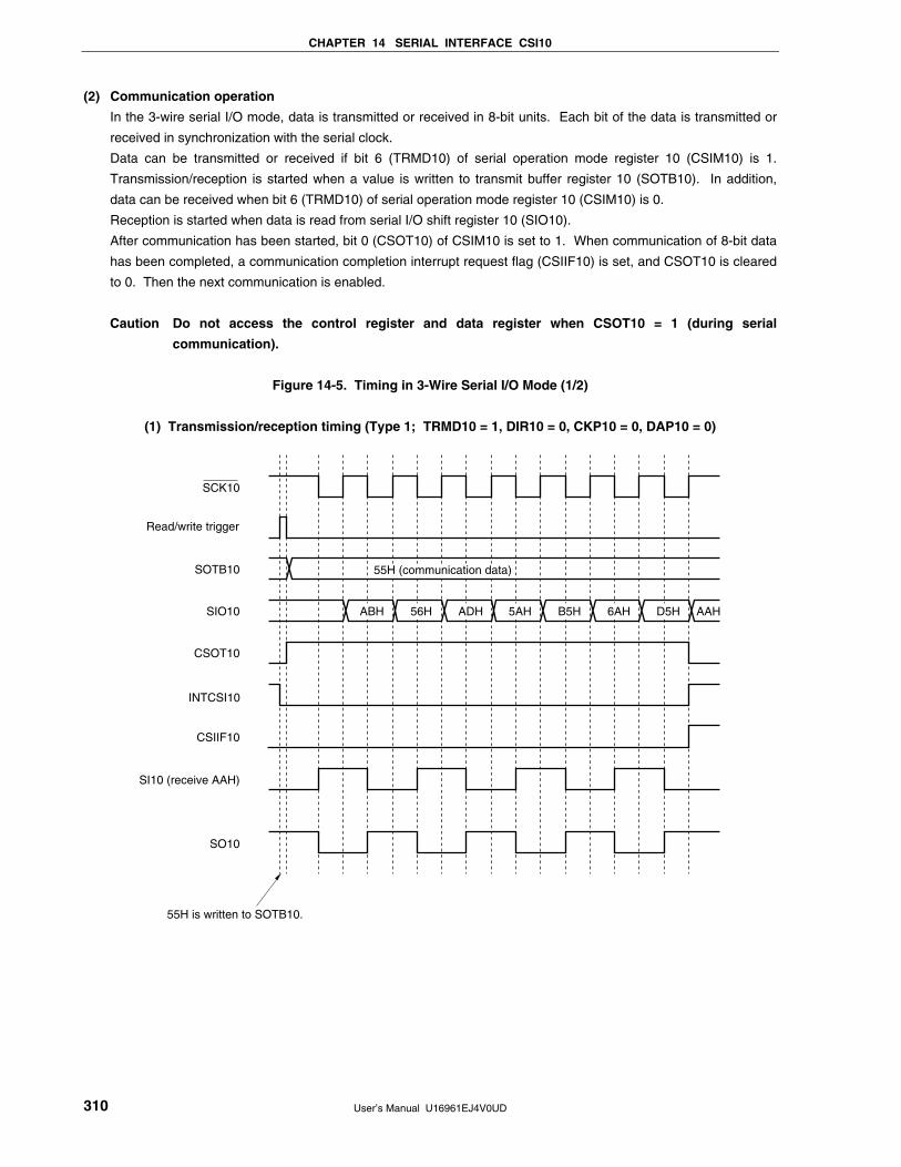
CHAPTER 14 SERIAL INTERFACE CSI10
User’s Manual U16961EJ4V0UD 310
(2) Communication operation
In the 3-wire serial I/O mode, data is transmitted or received in 8-bit units. Each bit of the data is transmitted or
received in synchronization with the serial clock.
Data can be transmitted or received if bit 6 (TRMD10) of serial operation mode register 10 (CSIM10) is 1.
Transmission/reception is started when a value is written to transmit buffer register 10 (SOTB10). In addition,
data can be received when bit 6 (TRMD10) of serial operation mode register 10 (CSIM10) is 0.
Reception is started when data is read from serial I/O shift register 10 (SIO10).
After communication has been started, bit 0 (CSOT10) of CSIM10 is set to 1. When communication of 8-bit data
has been completed, a communication completion interrupt request flag (CSIIF10) is set, and CSOT10 is cleared
to 0. Then the next communication is enabled.
Caution Do not access the control register and data register when CSOT10 = 1 (during serial
communication).
Figure 14-5. Timing in 3-Wire Serial I/O Mode (1/2)
(1) Transmission/reception timing (Type 1; TRMD10 = 1, DIR10 = 0, CKP10 = 0, DAP10 = 0)
AAHABH 56H ADH 5AH B5H 6AH D5H
55H (communication data)
55H is written to SOTB10.
SCK10
SOTB10
SIO10
CSOT10
CSIIF10
SO10
SI10 (receive AAH)
Read/write trigger
INTCSI10
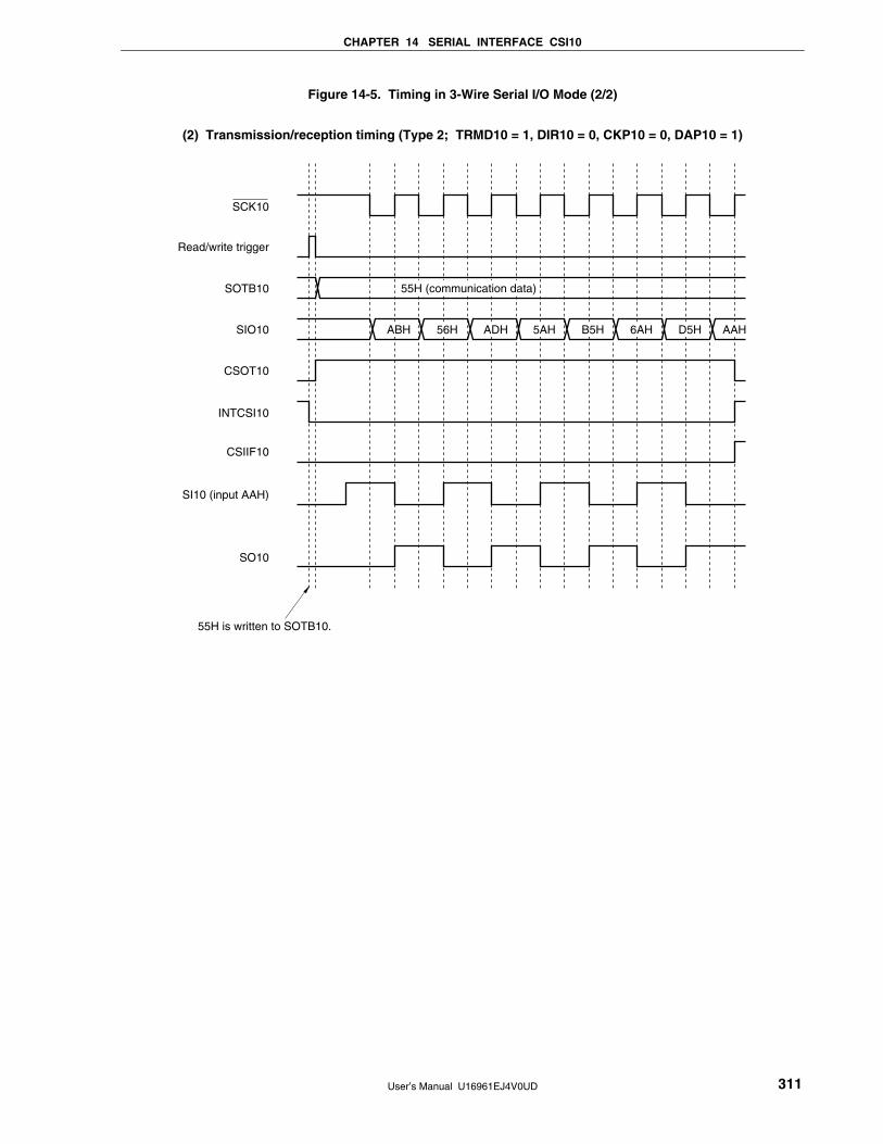
CHAPTER 14 SERIAL INTERFACE CSI10
User’s Manual U16961EJ4V0UD 311
Figure 14-5. Timing in 3-Wire Serial I/O Mode (2/2)
(2) Transmission/reception timing (Type 2; TRMD10 = 1, DIR10 = 0, CKP10 = 0, DAP10 = 1)
ABH 56H ADH 5AH B5H 6AH D5H
SCK10
SOTB10
SIO10
CSOT10
CSIIF10
SO10
SI10 (input AAH)
AAH
55H (communication data)
55H is written to SOTB10.
Read/write trigger
INTCSI10
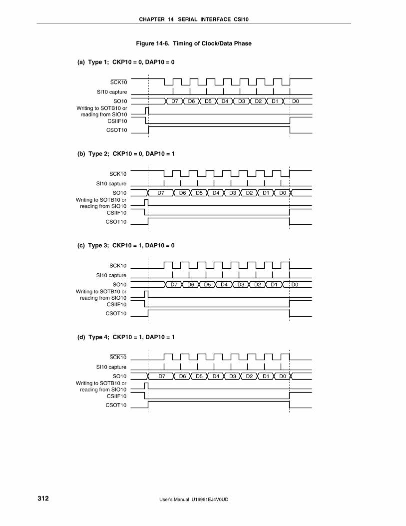
CHAPTER 14 SERIAL INTERFACE CSI10
User’s Manual U16961EJ4V0UD 312
Figure 14-6. Timing of Clock/Data Phase
(a) Type 1; CKP10 = 0, DAP10 = 0
D7 D6 D5 D4 D3 D2 D1 D0
SCK10
SO10 Writing to SOTB10 or
reading from SIO10
SI10 capture
CSIIF10
CSOT10
(b) Type 2; CKP10 = 0, DAP10 = 1
D7 D6 D5 D4 D3 D2 D1 D0
SCK10
SO10Writing to SOTB10 or
reading from SIO10
SI10 capture
CSIIF10
CSOT10
(c) Type 3; CKP10 = 1, DAP10 = 0
D7 D6 D5 D4 D3 D2 D1 D0
SCK10
SO10Writing to SOTB10 or
reading from SIO10
SI10 capture
CSIIF10
CSOT10
(d) Type 4; CKP10 = 1, DAP10 = 1
D7 D6 D5 D4 D3 D2 D1 D0
SCK10
SO10Writing to SOTB10 or
reading from SIO10
SI10 capture
CSIIF10
CSOT10
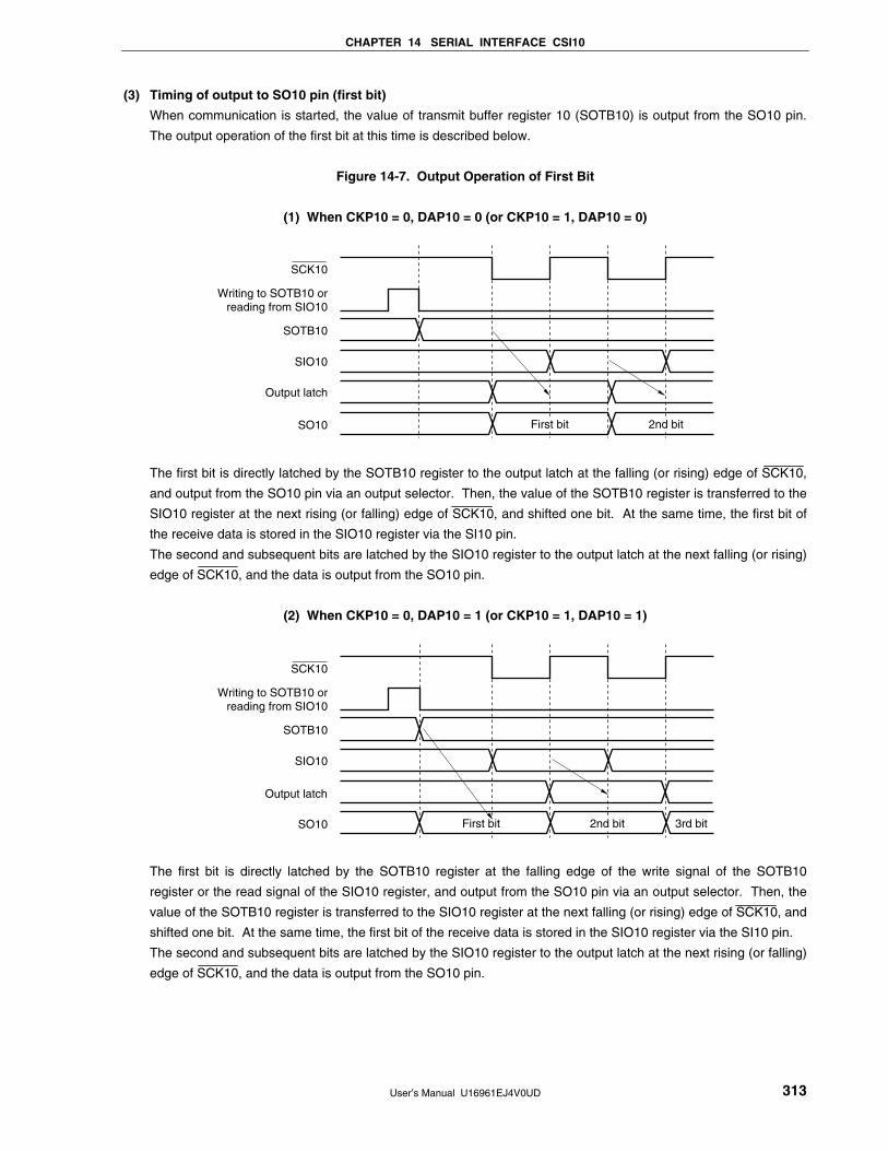
CHAPTER 14 SERIAL INTERFACE CSI10
User’s Manual U16961EJ4V0UD 313
(3) Timing of output to SO10 pin (first bit)
When communication is started, the value of transmit buffer register 10 (SOTB10) is output from the SO10 pin.
The output operation of the first bit at this time is described below.
Figure 14-7. Output Operation of First Bit
(1) When CKP10 = 0, DAP10 = 0 (or CKP10 = 1, DAP10 = 0)
SCK10
SOTB10
SIO10
SO10
Writing to SOTB10 orreading from SIO10
First bit 2nd bit
Output latch
The first bit is directly latched by the SOTB10 register to the output latch at the falling (or rising) edge of SCK10,
and output from the SO10 pin via an output selector. Then, the value of the SOTB10 register is transferred to the
SIO10 register at the next rising (or falling) edge of SCK10, and shifted one bit. At the same time, the first bit of
the receive data is stored in the SIO10 register via the SI10 pin.
The second and subsequent bits are latched by the SIO10 register to the output latch at the next falling (or rising)
edge of SCK10, and the data is output from the SO10 pin.
(2) When CKP10 = 0, DAP10 = 1 (or CKP10 = 1, DAP10 = 1)
SCK10
SOTB10
SIO10
SO10
Writing to SOTB10 orreading from SIO10
First bit 2nd bit 3rd bit
Output latch
The first bit is directly latched by the SOTB10 register at the falling edge of the write signal of the SOTB10
register or the read signal of the SIO10 register, and output from the SO10 pin via an output selector. Then, the
value of the SOTB10 register is transferred to the SIO10 register at the next falling (or rising) edge of SCK10, and
shifted one bit. At the same time, the first bit of the receive data is stored in the SIO10 register via the SI10 pin.
The second and subsequent bits are latched by the SIO10 register to the output latch at the next rising (or falling)
edge of SCK10, and the data is output from the SO10 pin.
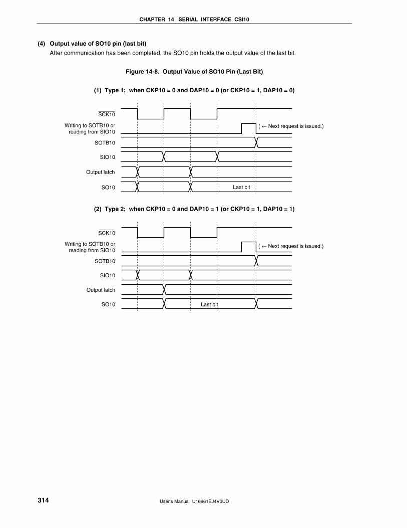
CHAPTER 14 SERIAL INTERFACE CSI10
User’s Manual U16961EJ4V0UD 314
(4) Output value of SO10 pin (last bit)
After communication has been completed, the SO10 pin holds the output value of the last bit.
Figure 14-8. Output Value of SO10 Pin (Last Bit)
(1) Type 1; when CKP10 = 0 and DAP10 = 0 (or CKP10 = 1, DAP10 = 0)
SCK10
SOTB10
SIO10
SO10
Writing to SOTB10 orreading from SIO10
( ← Next request is issued.)
Last bit
Output latch
(2) Type 2; when CKP10 = 0 and DAP10 = 1 (or CKP10 = 1, DAP10 = 1)
SCK10
SOTB10
SIO10
SO10 Last bit
Writing to SOTB10 orreading from SIO10
( ← Next request is issued.)
Output latch
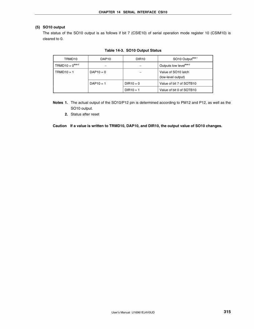
CHAPTER 14 SERIAL INTERFACE CSI10
User’s Manual U16961EJ4V0UD 315
(5) SO10 output
The status of the SO10 output is as follows if bit 7 (CSIE10) of serial operation mode register 10 (CSIM10) is
cleared to 0.
Table 14-3. SO10 Output Status
TRMD10 DAP10 DIR10 SO10 OutputNote 1
TRMD10 = 0Note 2 − − Outputs low levelNote 2
DAP10 = 0 − Value of SO10 latch
(low-level output)
DIR10 = 0 Value of bit 7 of SOTB10
TRMD10 = 1
DAP10 = 1
DIR10 = 1 Value of bit 0 of SOTB10
Notes 1. The actual output of the SO10/P12 pin is determined according to PM12 and P12, as well as the
SO10 output.
2. Status after reset
Caution If a value is written to TRMD10, DAP10, and DIR10, the output value of SO10 changes.
User’s Manual U16961EJ4V0UD 316
CHAPTER 15 INTERRUPT FUNCTIONS 15.1 Interrupt Function Types
The following two types of interrupt functions are used. (1) Maskable interrupts
These interrupts undergo mask control. Maskable interrupts can be divided into a high interrupt priority group and a low interrupt priority group by setting the priority specification flag registers (PR0L, PR0H, PR1L). Multiple interrupt servicing can be applied to low-priority interrupts when high-priority interrupts are generated. If two or more interrupts with the same priority are generated simultaneously, each interrupt is serviced according to its predetermined priority (see Table 15-1). A standby release signal is generated and STOP and HALT modes are released. Seven external interrupt requests and 15 internal interrupt requests are provided as maskable interrupts.
(2) Software interrupt
This is a vectored interrupt generated by executing the BRK instruction. It is acknowledged even when interrupts are disabled. The software interrupt does not undergo interrupt priority control.
15.2 Interrupt Sources and Configuration
A total of 23 interrupt sources exist for maskable and software interrupts. In addition, maximum total of 5 reset sources are also provided (see Table 15-1).
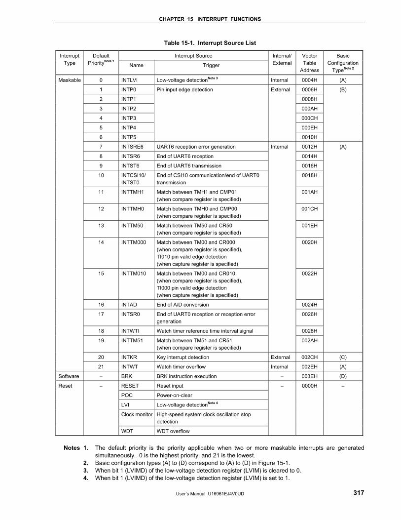
CHAPTER 15 INTERRUPT FUNCTIONS
User’s Manual U16961EJ4V0UD 317
Table 15-1. Interrupt Source List
Interrupt Source Interrupt Type
Default PriorityNote 1 Name Trigger
Internal/ External
Vector Table
Address
Basic Configuration
TypeNote 2
0 INTLVI Low-voltage detectionNote 3 Internal 0004H (A)
1 INTP0 0006H
2 INTP1 0008H
3 INTP2 000AH
4 INTP3 000CH
5 INTP4 000EH
6 INTP5
Pin input edge detection External
0010H
(B)
7 INTSRE6 UART6 reception error generation 0012H
8 INTSR6 End of UART6 reception 0014H
9 INTST6 End of UART6 transmission 0016H
10 INTCSI10/ INTST0
End of CSI10 communication/end of UART0 transmission
0018H
11 INTTMH1 Match between TMH1 and CMP01 (when compare register is specified)
001AH
12 INTTMH0 Match between TMH0 and CMP00 (when compare register is specified)
001CH
13 INTTM50 Match between TM50 and CR50 (when compare register is specified)
001EH
14 INTTM000 Match between TM00 and CR000 (when compare register is specified), TI010 pin valid edge detection (when capture register is specified)
0020H
15 INTTM010 Match between TM00 and CR010 (when compare register is specified), TI000 pin valid edge detection (when capture register is specified)
0022H
16 INTAD End of A/D conversion 0024H
17 INTSR0 End of UART0 reception or reception error generation
0026H
18 INTWTI Watch timer reference time interval signal 0028H
19 INTTM51 Match between TM51 and CR51 (when compare register is specified)
Internal
002AH
(A)
20 INTKR Key interrupt detection External 002CH (C)
Maskable
21 INTWT Watch timer overflow Internal 002EH (A)
Software − BRK BRK instruction execution − 003EH (D)
RESET Reset input
POC Power-on-clear
LVI Low-voltage detectionNote 4
Clock monitor High-speed system clock oscillation stop detection
Reset −
WDT WDT overflow
− 0000H −
Notes 1. The default priority is the priority applicable when two or more maskable interrupts are generated
simultaneously. 0 is the highest priority, and 21 is the lowest. 2. Basic configuration types (A) to (D) correspond to (A) to (D) in Figure 15-1. 3. When bit 1 (LVIMD) of the low-voltage detection register (LVIM) is cleared to 0. 4. When bit 1 (LVIMD) of the low-voltage detection register (LVIM) is set to 1.
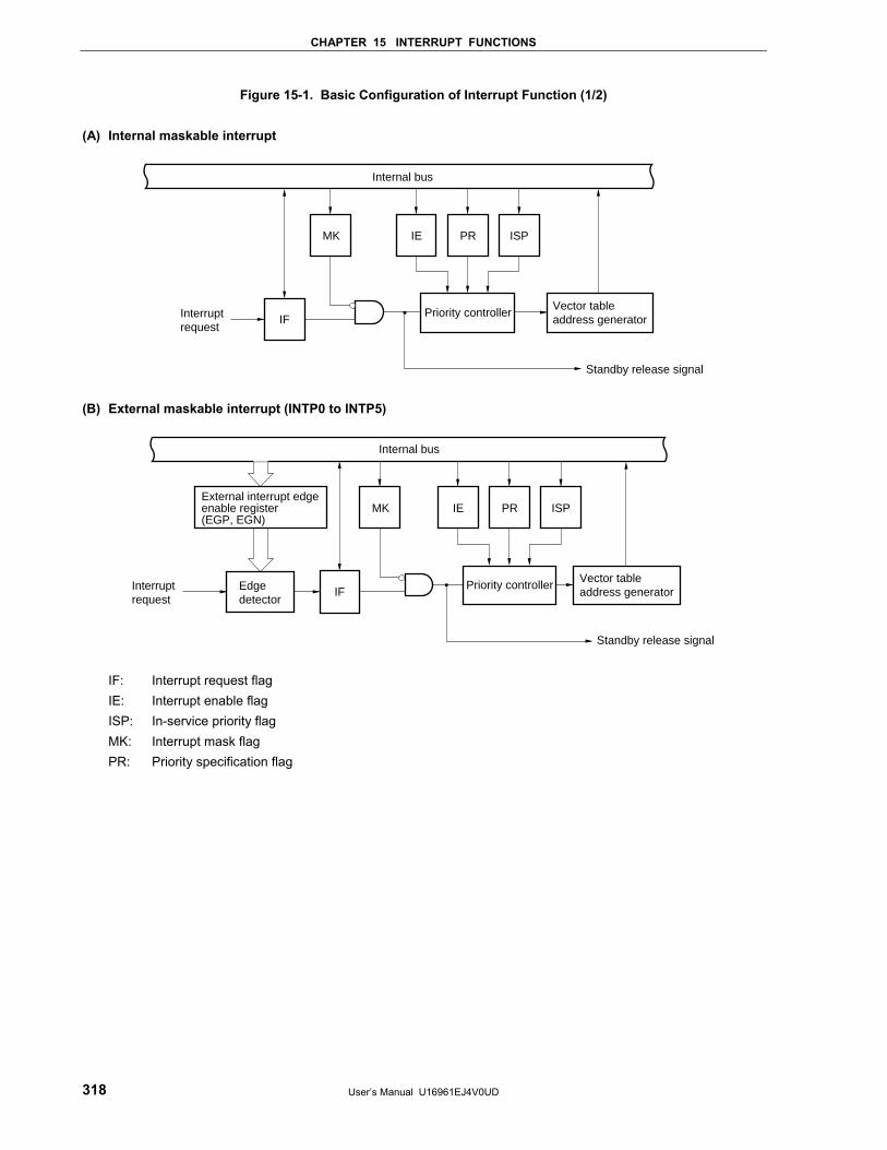
CHAPTER 15 INTERRUPT FUNCTIONS
User’s Manual U16961EJ4V0UD 318
Figure 15-1. Basic Configuration of Interrupt Function (1/2) (A) Internal maskable interrupt
Internal bus
Interrupt request
IF
MK IE PR ISP
Priority controllerVector table address generator
Standby release signal (B) External maskable interrupt (INTP0 to INTP5)
Internal bus
Interrupt request
IF
MK IE PR ISP
Priority controllerVector table address generator
Standby release signal
External interrupt edge enable register (EGP, EGN)
Edge detector
IF: Interrupt request flag IE: Interrupt enable flag ISP: In-service priority flag MK: Interrupt mask flag PR: Priority specification flag
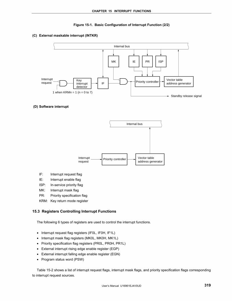
CHAPTER 15 INTERRUPT FUNCTIONS
User’s Manual U16961EJ4V0UD 319
Figure 15-1. Basic Configuration of Interrupt Function (2/2) (C) External maskable interrupt (INTKR)
IF
MK IE PR ISP
Internal bus
Interrupt request Priority controller
Vector table address generator
Standby release signal
Key interrupt detector
1 when KRMn = 1 (n = 0 to 7)
(D) Software interrupt
Internal bus
Interrupt request
Priority controller Vector table address generator
IF: Interrupt request flag IE: Interrupt enable flag ISP: In-service priority flag MK: Interrupt mask flag PR: Priority specification flag KRM: Key return mode register
15.3 Registers Controlling Interrupt Functions
The following 6 types of registers are used to control the interrupt functions. • Interrupt request flag registers (IF0L, IF0H, IF1L) • Interrupt mask flag registers (MK0L, MK0H, MK1L) • Priority specification flag registers (PR0L, PR0H, PR1L) • External interrupt rising edge enable register (EGP) • External interrupt falling edge enable register (EGN) • Program status word (PSW) Table 15-2 shows a list of interrupt request flags, interrupt mask flags, and priority specification flags corresponding
to interrupt request sources.
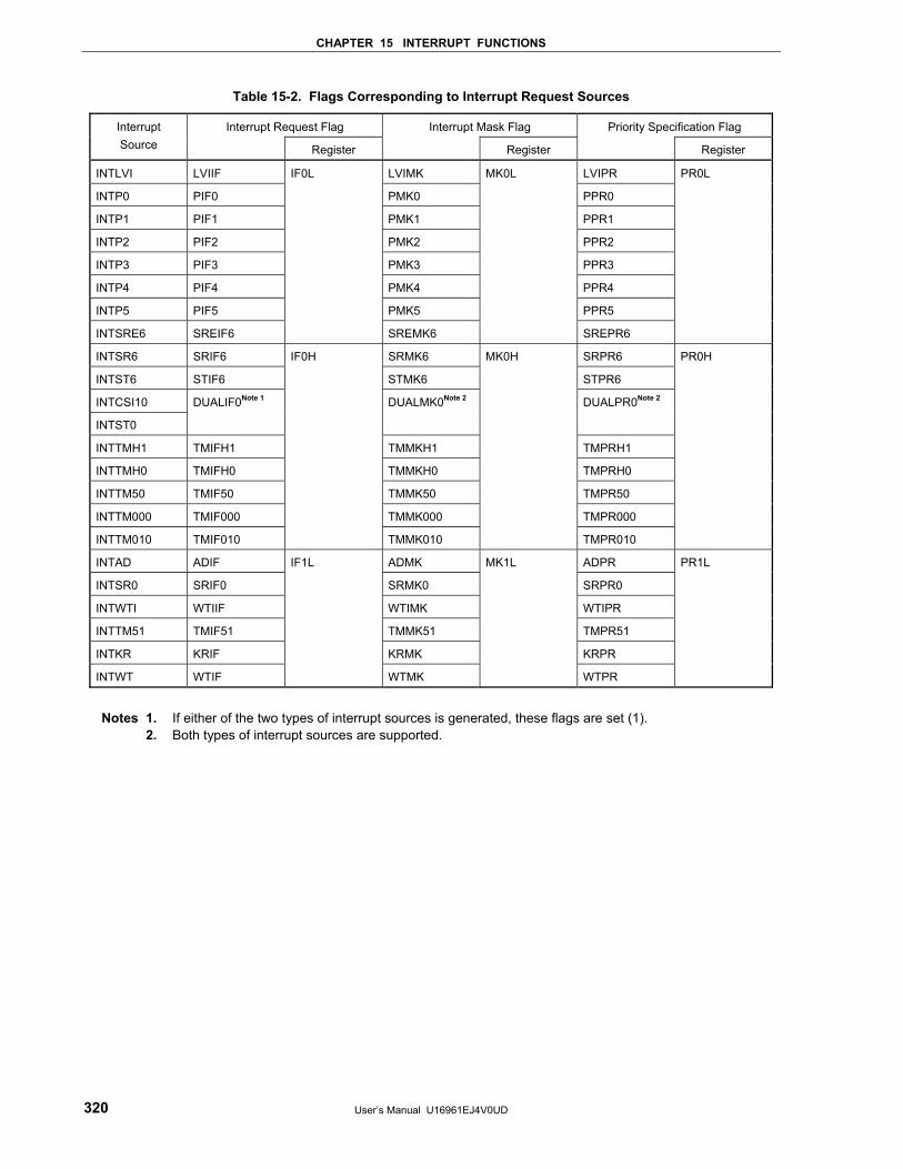
CHAPTER 15 INTERRUPT FUNCTIONS
User’s Manual U16961EJ4V0UD 320
Table 15-2. Flags Corresponding to Interrupt Request Sources
Interrupt Request Flag Interrupt Mask Flag Priority Specification Flag Interrupt Source Register Register Register
INTLVI LVIIF IF0L LVIMK MK0L LVIPR PR0L
INTP0 PIF0 PMK0 PPR0
INTP1 PIF1 PMK1 PPR1
INTP2 PIF2 PMK2 PPR2
INTP3 PIF3 PMK3 PPR3
INTP4 PIF4 PMK4 PPR4
INTP5 PIF5 PMK5 PPR5
INTSRE6 SREIF6 SREMK6 SREPR6
INTSR6 SRIF6 IF0H SRMK6 MK0H SRPR6 PR0H
INTST6 STIF6 STMK6 STPR6
INTCSI10 DUALIF0Note 1 DUALMK0Note 2 DUALPR0Note 2
INTST0
INTTMH1 TMIFH1 TMMKH1 TMPRH1
INTTMH0 TMIFH0 TMMKH0 TMPRH0
INTTM50 TMIF50 TMMK50 TMPR50
INTTM000 TMIF000 TMMK000 TMPR000
INTTM010 TMIF010 TMMK010 TMPR010
INTAD ADIF IF1L ADMK MK1L ADPR PR1L
INTSR0 SRIF0 SRMK0 SRPR0
INTWTI WTIIF WTIMK WTIPR
INTTM51 TMIF51 TMMK51 TMPR51
INTKR KRIF KRMK KRPR
INTWT WTIF WTMK WTPR
Notes 1. If either of the two types of interrupt sources is generated, these flags are set (1). 2. Both types of interrupt sources are supported.
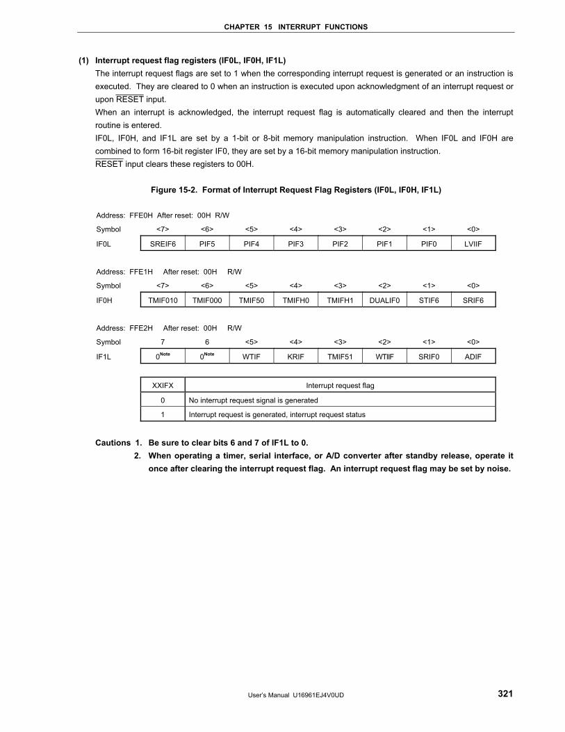
CHAPTER 15 INTERRUPT FUNCTIONS
User’s Manual U16961EJ4V0UD 321
(1) Interrupt request flag registers (IF0L, IF0H, IF1L) The interrupt request flags are set to 1 when the corresponding interrupt request is generated or an instruction is executed. They are cleared to 0 when an instruction is executed upon acknowledgment of an interrupt request or upon RESET input. When an interrupt is acknowledged, the interrupt request flag is automatically cleared and then the interrupt routine is entered. IF0L, IF0H, and IF1L are set by a 1-bit or 8-bit memory manipulation instruction. When IF0L and IF0H are combined to form 16-bit register IF0, they are set by a 16-bit memory manipulation instruction. RESET input clears these registers to 00H.
Figure 15-2. Format of Interrupt Request Flag Registers (IF0L, IF0H, IF1L)
Address: FFE0H After reset: 00H R/W
Symbol <7> <6> <5> <4> <3> <2> <1> <0>
IF0L SREIF6 PIF5 PIF4 PIF3 PIF2 PIF1 PIF0 LVIIF
Address: FFE1H After reset: 00H R/W
Symbol <7> <6> <5> <4> <3> <2> <1> <0>
IF0H TMIF010 TMIF000 TMIF50 TMIFH0 TMIFH1 DUALIF0 STIF6 SRIF6
Address: FFE2H After reset: 00H R/W
Symbol 7 6 <5> <4> <3> <2> <1> <0>
IF1L 0Note 0Note WTIF KRIF TMIF51 WTIIF SRIF0 ADIF
XXIFX Interrupt request flag
0 No interrupt request signal is generated
1 Interrupt request is generated, interrupt request status
Cautions 1. Be sure to clear bits 6 and 7 of IF1L to 0. 2. When operating a timer, serial interface, or A/D converter after standby release, operate it
once after clearing the interrupt request flag. An interrupt request flag may be set by noise.
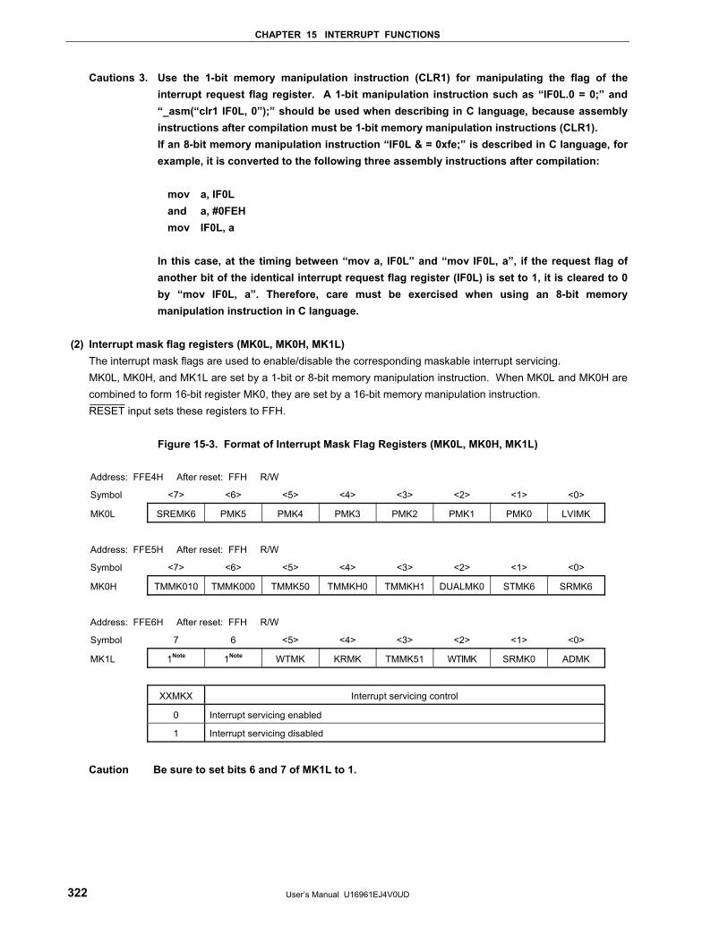
CHAPTER 15 INTERRUPT FUNCTIONS
User’s Manual U16961EJ4V0UD 322
Cautions 3. Use the 1-bit memory manipulation instruction (CLR1) for manipulating the flag of the interrupt request flag register. A 1-bit manipulation instruction such as “IF0L.0 = 0;” and “_asm(“clr1 IF0L, 0”);” should be used when describing in C language, because assembly instructions after compilation must be 1-bit memory manipulation instructions (CLR1).
If an 8-bit memory manipulation instruction “IF0L & = 0xfe;” is described in C language, for example, it is converted to the following three assembly instructions after compilation:
mov a, IF0L and a, #0FEH mov IF0L, a In this case, at the timing between “mov a, IF0L” and “mov IF0L, a”, if the request flag of
another bit of the identical interrupt request flag register (IF0L) is set to 1, it is cleared to 0 by “mov IF0L, a”. Therefore, care must be exercised when using an 8-bit memory manipulation instruction in C language.
(2) Interrupt mask flag registers (MK0L, MK0H, MK1L)
The interrupt mask flags are used to enable/disable the corresponding maskable interrupt servicing. MK0L, MK0H, and MK1L are set by a 1-bit or 8-bit memory manipulation instruction. When MK0L and MK0H are combined to form 16-bit register MK0, they are set by a 16-bit memory manipulation instruction. RESET input sets these registers to FFH.
Figure 15-3. Format of Interrupt Mask Flag Registers (MK0L, MK0H, MK1L)
Address: FFE4H After reset: FFH R/W
Symbol <7> <6> <5> <4> <3> <2> <1> <0>
MK0L SREMK6 PMK5 PMK4 PMK3 PMK2 PMK1 PMK0 LVIMK
Address: FFE5H After reset: FFH R/W
Symbol <7> <6> <5> <4> <3> <2> <1> <0>
MK0H TMMK010 TMMK000 TMMK50 TMMKH0 TMMKH1 DUALMK0 STMK6 SRMK6
Address: FFE6H After reset: FFH R/W
Symbol 7 6 <5> <4> <3> <2> <1> <0>
MK1L 1Note 1Note WTMK KRMK TMMK51 WTIMK SRMK0 ADMK
XXMKX Interrupt servicing control
0 Interrupt servicing enabled
1 Interrupt servicing disabled
Caution Be sure to set bits 6 and 7 of MK1L to 1.
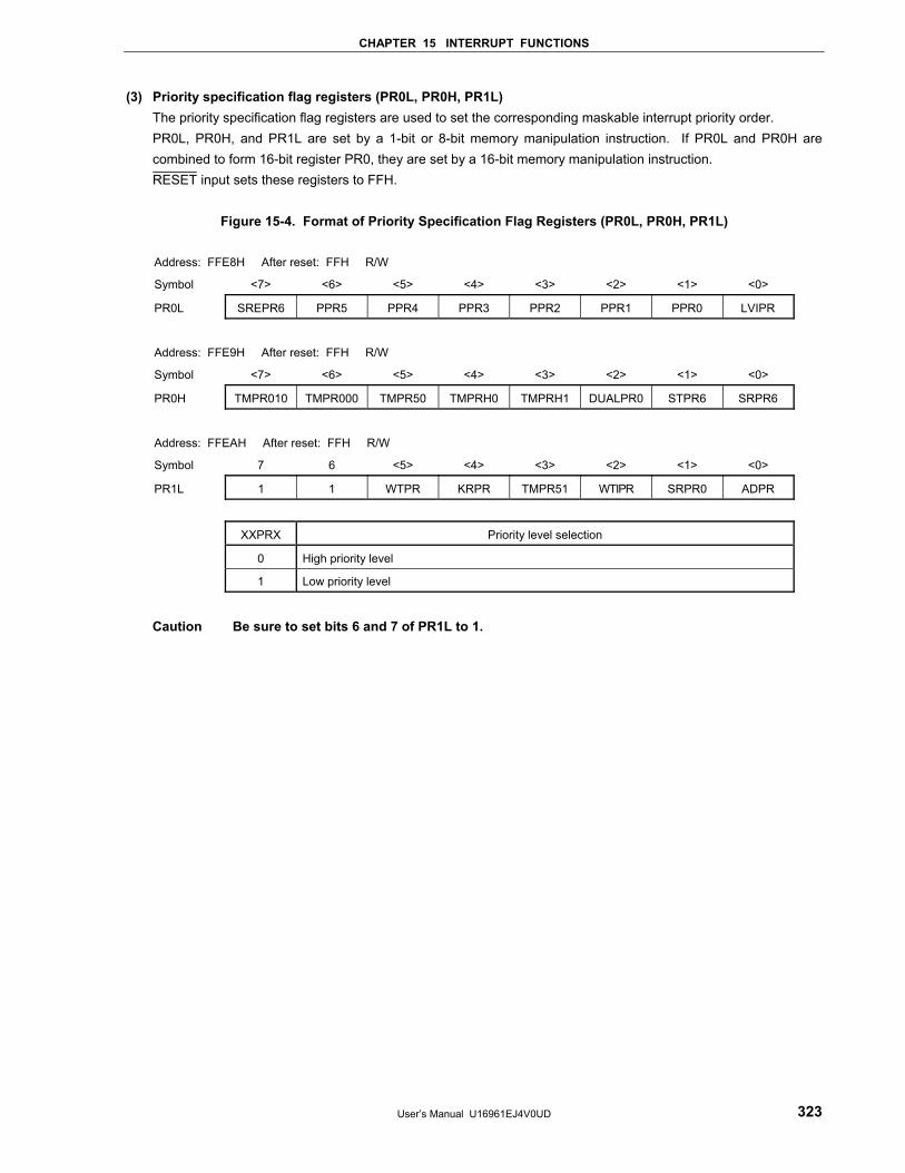
CHAPTER 15 INTERRUPT FUNCTIONS
User’s Manual U16961EJ4V0UD 323
(3) Priority specification flag registers (PR0L, PR0H, PR1L) The priority specification flag registers are used to set the corresponding maskable interrupt priority order. PR0L, PR0H, and PR1L are set by a 1-bit or 8-bit memory manipulation instruction. If PR0L and PR0H are combined to form 16-bit register PR0, they are set by a 16-bit memory manipulation instruction. RESET input sets these registers to FFH.
Figure 15-4. Format of Priority Specification Flag Registers (PR0L, PR0H, PR1L)
Address: FFE8H After reset: FFH R/W
Symbol <7> <6> <5> <4> <3> <2> <1> <0>
PR0L SREPR6 PPR5 PPR4 PPR3 PPR2 PPR1 PPR0 LVIPR
Address: FFE9H After reset: FFH R/W
Symbol <7> <6> <5> <4> <3> <2> <1> <0>
PR0H TMPR010 TMPR000 TMPR50 TMPRH0 TMPRH1 DUALPR0 STPR6 SRPR6
Address: FFEAH After reset: FFH R/W
Symbol 7 6 <5> <4> <3> <2> <1> <0>
PR1L 1 1 WTPR KRPR TMPR51 WTIPR SRPR0 ADPR
XXPRX Priority level selection
0 High priority level
1 Low priority level
Caution Be sure to set bits 6 and 7 of PR1L to 1.
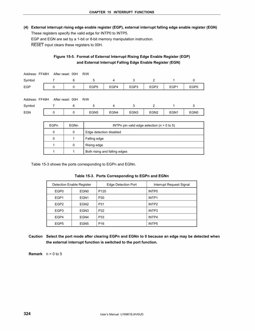
CHAPTER 15 INTERRUPT FUNCTIONS
User’s Manual U16961EJ4V0UD 324
(4) External interrupt rising edge enable register (EGP), external interrupt falling edge enable register (EGN) These registers specify the valid edge for INTP0 to INTP5. EGP and EGN are set by a 1-bit or 8-bit memory manipulation instruction. RESET input clears these registers to 00H.
Figure 15-5. Format of External Interrupt Rising Edge Enable Register (EGP) and External Interrupt Falling Edge Enable Register (EGN)
Address: FF48H After reset: 00H R/W
Symbol 7 6 5 4 3 2 1 0
EGP 0 0 EGP5 EGP4 EGP3 EGP2 EGP1 EGP0
Address: FF49H After reset: 00H R/W
Symbol 7 6 5 4 3 2 1 0
EGN 0 0 EGN5 EGN4 EGN3 EGN2 EGN1 EGN0
EGPn EGNn INTPn pin valid edge selection (n = 0 to 5)
0 0 Edge detection disabled
0 1 Falling edge
1 0 Rising edge
1 1 Both rising and falling edges
Table 15-3 shows the ports corresponding to EGPn and EGNn.
Table 15-3. Ports Corresponding to EGPn and EGNn
Detection Enable Register Edge Detection Port Interrupt Request Signal
EGP0 EGN0 P120 INTP0
EGP1 EGN1 P30 INTP1
EGP2 EGN2 P31 INTP2
EGP3 EGN3 P32 INTP3
EGP4 EGN4 P33 INTP4
EGP5 EGN5 P16 INTP5
Caution Select the port mode after clearing EGPn and EGNn to 0 because an edge may be detected when
the external interrupt function is switched to the port function. Remark n = 0 to 5
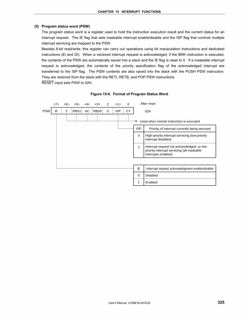
CHAPTER 15 INTERRUPT FUNCTIONS
User’s Manual U16961EJ4V0UD 325
(5) Program status word (PSW) The program status word is a register used to hold the instruction execution result and the current status for an interrupt request. The IE flag that sets maskable interrupt enable/disable and the ISP flag that controls multiple interrupt servicing are mapped to the PSW. Besides 8-bit read/write, this register can carry out operations using bit manipulation instructions and dedicated instructions (EI and DI). When a vectored interrupt request is acknowledged, if the BRK instruction is executed, the contents of the PSW are automatically saved into a stack and the IE flag is reset to 0. If a maskable interrupt request is acknowledged, the contents of the priority specification flag of the acknowledged interrupt are transferred to the ISP flag. The PSW contents are also saved into the stack with the PUSH PSW instruction. They are restored from the stack with the RETI, RETB, and POP PSW instructions. RESET input sets PSW to 02H.
Figure 15-6. Format of Program Status Word
<7>
IE
<6>
Z
<5>
RBS1
<4>
AC
<3>
RBS0
2
0
<1>
ISP
0
CYPSW
After reset
02H
ISP
High-priority interrupt servicing (low-priority interrupt disabled)
IE
0
1
Disabled
Priority of interrupt currently being serviced
Interrupt request acknowledgment enable/disable
Used when normal instruction is executed
Enabled
Interrupt request not acknowledged, or low-priority interrupt servicing (all maskable interrupts enabled)
0
1
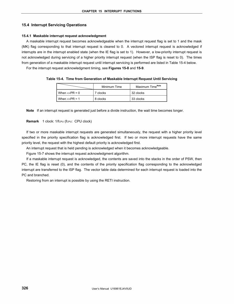
CHAPTER 15 INTERRUPT FUNCTIONS
User’s Manual U16961EJ4V0UD 326
15.4 Interrupt Servicing Operations 15.4.1 Maskable interrupt request acknowledgment
A maskable interrupt request becomes acknowledgeable when the interrupt request flag is set to 1 and the mask (MK) flag corresponding to that interrupt request is cleared to 0. A vectored interrupt request is acknowledged if interrupts are in the interrupt enabled state (when the IE flag is set to 1). However, a low-priority interrupt request is not acknowledged during servicing of a higher priority interrupt request (when the ISP flag is reset to 0). The times from generation of a maskable interrupt request until interrupt servicing is performed are listed in Table 15-4 below.
For the interrupt request acknowledgment timing, see Figures 15-8 and 15-9.
Table 15-4. Time from Generation of Maskable Interrupt Request Until Servicing
Minimum Time Maximum TimeNote
When ××PR = 0 7 clocks 32 clocks
When ××PR = 1 8 clocks 33 clocks
Note If an interrupt request is generated just before a divide instruction, the wait time becomes longer.
Remark 1 clock: 1/fCPU (fCPU: CPU clock)
If two or more maskable interrupt requests are generated simultaneously, the request with a higher priority level
specified in the priority specification flag is acknowledged first. If two or more interrupt requests have the same priority level, the request with the highest default priority is acknowledged first.
An interrupt request that is held pending is acknowledged when it becomes acknowledgeable. Figure 15-7 shows the interrupt request acknowledgment algorithm. If a maskable interrupt request is acknowledged, the contents are saved into the stacks in the order of PSW, then
PC, the IE flag is reset (0), and the contents of the priority specification flag corresponding to the acknowledged interrupt are transferred to the ISP flag. The vector table data determined for each interrupt request is loaded into the PC and branched.
Restoring from an interrupt is possible by using the RETI instruction.
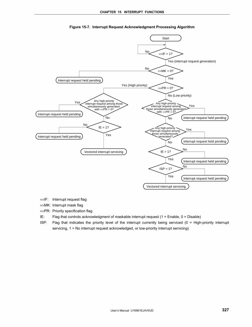
CHAPTER 15 INTERRUPT FUNCTIONS
User’s Manual U16961EJ4V0UD 327
Figure 15-7. Interrupt Request Acknowledgment Processing Algorithm
Start
××IF = 1?
××MK = 0?
××PR = 0?
IE = 1?
ISP = 1?
Interrupt request held pending
Yes
Yes
No
No
Yes (interrupt request generation)
Yes
No (Low priority)
No
No
Yes
Yes
No
IE = 1?
No
Any high-priority interrupt request among those
simultaneously generated with ××PR = 0?
Yes (High priority)
No
Yes
Yes
No
Vectored interrupt servicing
Interrupt request held pending
Interrupt request held pending
Interrupt request held pending
Interrupt request held pending
Interrupt request held pending
Interrupt request held pending
Vectored interrupt servicing
Any high-priority interrupt request among
those simultaneously generated?
Any high-priority interrupt request among
those simultaneously generated with ××PR = 0?
××IF: Interrupt request flag ××MK: Interrupt mask flag ××PR: Priority specification flag IE: Flag that controls acknowledgment of maskable interrupt request (1 = Enable, 0 = Disable) ISP: Flag that indicates the priority level of the interrupt currently being serviced (0 = High-priority interrupt
servicing, 1 = No interrupt request acknowledged, or low-priority interrupt servicing)
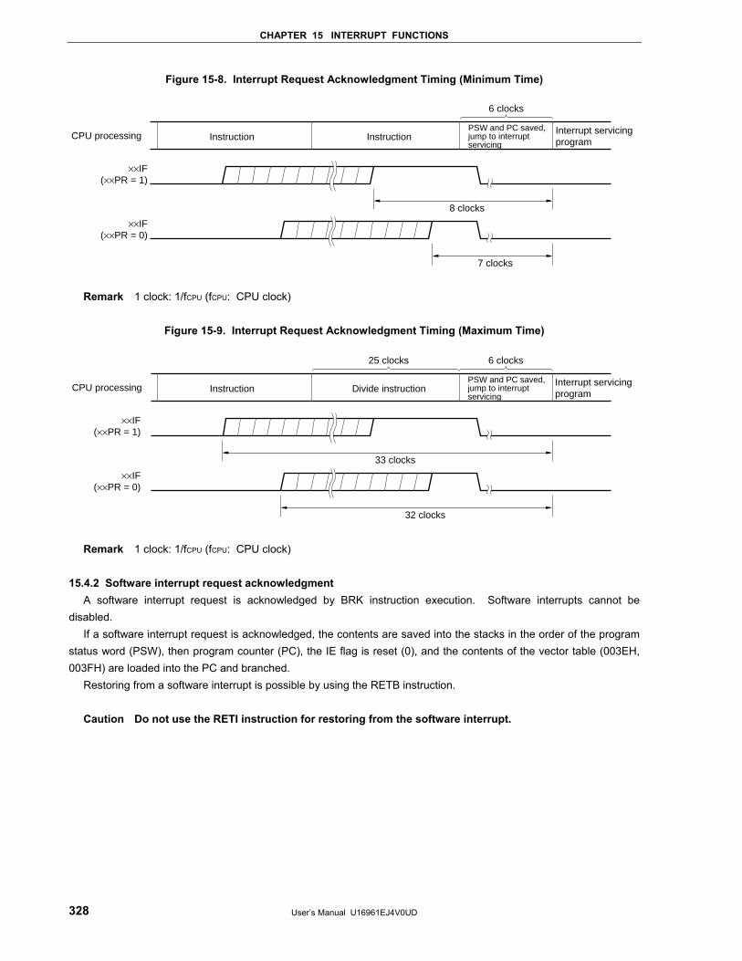
CHAPTER 15 INTERRUPT FUNCTIONS
User’s Manual U16961EJ4V0UD 328
Figure 15-8. Interrupt Request Acknowledgment Timing (Minimum Time)
8 clocks
7 clocks
Instruction InstructionPSW and PC saved, jump to interrupt servicing
Interrupt servicing program
CPU processing
××IF(××PR = 1)
××IF(××PR = 0)
6 clocks
Remark 1 clock: 1/fCPU (fCPU: CPU clock)
Figure 15-9. Interrupt Request Acknowledgment Timing (Maximum Time)
33 clocks
32 clocks
Instruction Divide instructionPSW and PC saved, jump to interrupt servicing
Interrupt servicing program
CPU processing
××IF(××PR = 1)
××IF(××PR = 0)
6 clocks25 clocks
Remark 1 clock: 1/fCPU (fCPU: CPU clock) 15.4.2 Software interrupt request acknowledgment
A software interrupt request is acknowledged by BRK instruction execution. Software interrupts cannot be disabled.
If a software interrupt request is acknowledged, the contents are saved into the stacks in the order of the program status word (PSW), then program counter (PC), the IE flag is reset (0), and the contents of the vector table (003EH, 003FH) are loaded into the PC and branched.
Restoring from a software interrupt is possible by using the RETB instruction.
Caution Do not use the RETI instruction for restoring from the software interrupt.
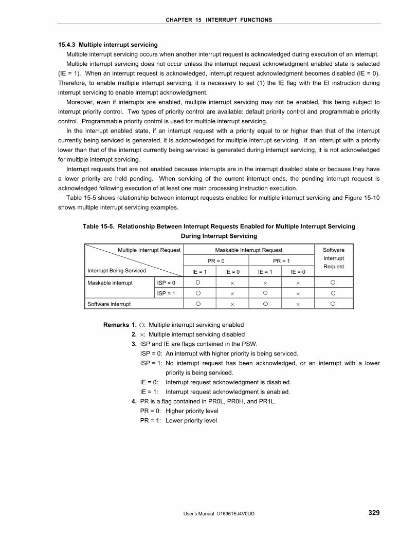
CHAPTER 15 INTERRUPT FUNCTIONS
User’s Manual U16961EJ4V0UD 329
15.4.3 Multiple interrupt servicing Multiple interrupt servicing occurs when another interrupt request is acknowledged during execution of an interrupt. Multiple interrupt servicing does not occur unless the interrupt request acknowledgment enabled state is selected
(IE = 1). When an interrupt request is acknowledged, interrupt request acknowledgment becomes disabled (IE = 0). Therefore, to enable multiple interrupt servicing, it is necessary to set (1) the IE flag with the EI instruction during interrupt servicing to enable interrupt acknowledgment.
Moreover, even if interrupts are enabled, multiple interrupt servicing may not be enabled, this being subject to interrupt priority control. Two types of priority control are available: default priority control and programmable priority control. Programmable priority control is used for multiple interrupt servicing.
In the interrupt enabled state, if an interrupt request with a priority equal to or higher than that of the interrupt currently being serviced is generated, it is acknowledged for multiple interrupt servicing. If an interrupt with a priority lower than that of the interrupt currently being serviced is generated during interrupt servicing, it is not acknowledged for multiple interrupt servicing.
Interrupt requests that are not enabled because interrupts are in the interrupt disabled state or because they have a lower priority are held pending. When servicing of the current interrupt ends, the pending interrupt request is acknowledged following execution of at least one main processing instruction execution.
Table 15-5 shows relationship between interrupt requests enabled for multiple interrupt servicing and Figure 15-10 shows multiple interrupt servicing examples.
Table 15-5. Relationship Between Interrupt Requests Enabled for Multiple Interrupt Servicing During Interrupt Servicing
Maskable Interrupt Request
PR = 0 PR = 1
Multiple Interrupt Request
Interrupt Being Serviced IE = 1 IE = 0 IE = 1 IE = 0
Software Interrupt Request
ISP = 0 × × × Maskable interrupt
ISP = 1 × ×
Software interrupt × ×
Remarks 1. : Multiple interrupt servicing enabled 2. ×: Multiple interrupt servicing disabled
3. ISP and IE are flags contained in the PSW. ISP = 0: An interrupt with higher priority is being serviced. ISP = 1: No interrupt request has been acknowledged, or an interrupt with a lower
priority is being serviced. IE = 0: Interrupt request acknowledgment is disabled. IE = 1: Interrupt request acknowledgment is enabled. 4. PR is a flag contained in PR0L, PR0H, and PR1L. PR = 0: Higher priority level PR = 1: Lower priority level
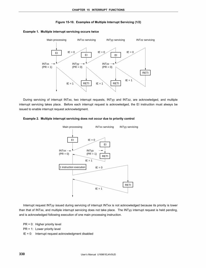
CHAPTER 15 INTERRUPT FUNCTIONS
User’s Manual U16961EJ4V0UD 330
Figure 15-10. Examples of Multiple Interrupt Servicing (1/2)
Example 1. Multiple interrupt servicing occurs twice
Main processing INTxx servicing INTyy servicing INTzz servicing
EIEI EI
RETI RETI
RETI
INTxx(PR = 1)
INTyy(PR = 0)
INTzz(PR = 0)
IE = 0 IE = 0 IE = 0
IE = 1 IE = 1IE = 1
During servicing of interrupt INTxx, two interrupt requests, INTyy and INTzz, are acknowledged, and multiple interrupt servicing takes place. Before each interrupt request is acknowledged, the EI instruction must always be issued to enable interrupt request acknowledgment.
Example 2. Multiple interrupt servicing does not occur due to priority control
Main processing INTxx servicing INTyy servicing
INTxx(PR = 0)
INTyy(PR = 1)
EI
RETI
IE = 0
IE = 0EI
1 instruction execution
RETIIE = 1
IE = 1
Interrupt request INTyy issued during servicing of interrupt INTxx is not acknowledged because its priority is lower than that of INTxx, and multiple interrupt servicing does not take place. The INTyy interrupt request is held pending, and is acknowledged following execution of one main processing instruction.
PR = 0: Higher priority level PR = 1: Lower priority level IE = 0: Interrupt request acknowledgment disabled
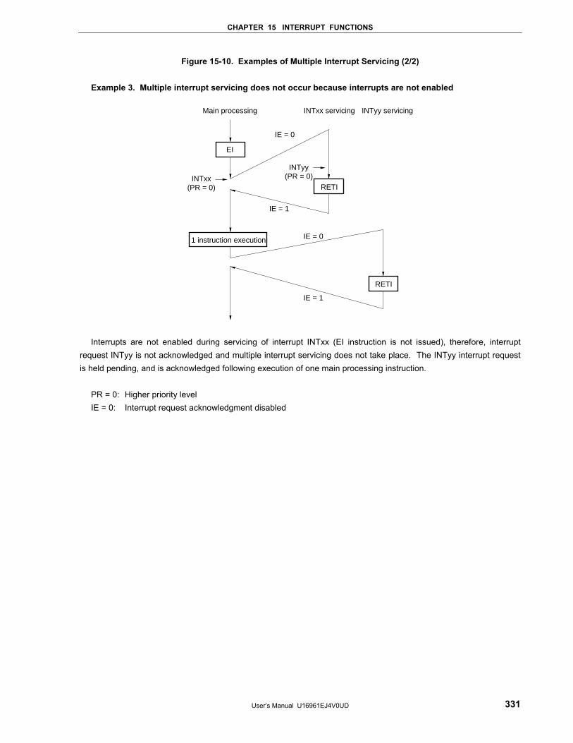
CHAPTER 15 INTERRUPT FUNCTIONS
User’s Manual U16961EJ4V0UD 331
Figure 15-10. Examples of Multiple Interrupt Servicing (2/2)
Example 3. Multiple interrupt servicing does not occur because interrupts are not enabled
Main processing INTxx servicing INTyy servicing
EI
1 instruction execution
RETI
RETI
INTxx(PR = 0)
INTyy(PR = 0)
IE = 0
IE = 0
IE = 1
IE = 1
Interrupts are not enabled during servicing of interrupt INTxx (EI instruction is not issued), therefore, interrupt request INTyy is not acknowledged and multiple interrupt servicing does not take place. The INTyy interrupt request is held pending, and is acknowledged following execution of one main processing instruction.
PR = 0: Higher priority level IE = 0: Interrupt request acknowledgment disabled
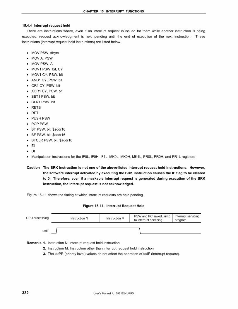
CHAPTER 15 INTERRUPT FUNCTIONS
User’s Manual U16961EJ4V0UD 332
15.4.4 Interrupt request hold There are instructions where, even if an interrupt request is issued for them while another instruction is being
executed, request acknowledgment is held pending until the end of execution of the next instruction. These instructions (interrupt request hold instructions) are listed below.
• MOV PSW, #byte • MOV A, PSW • MOV PSW, A • MOV1 PSW. bit, CY • MOV1 CY, PSW. bit • AND1 CY, PSW. bit • OR1 CY, PSW. bit • XOR1 CY, PSW. bit • SET1 PSW. bit • CLR1 PSW. bit • RETB • RETI • PUSH PSW • POP PSW • BT PSW. bit, $addr16 • BF PSW. bit, $addr16 • BTCLR PSW. bit, $addr16 • EI • DI • Manipulation instructions for the IF0L, IF0H, IF1L, MK0L, MK0H, MK1L, PR0L, PR0H, and PR1L registers
Caution The BRK instruction is not one of the above-listed interrupt request hold instructions. However,
the software interrupt activated by executing the BRK instruction causes the IE flag to be cleared to 0. Therefore, even if a maskable interrupt request is generated during execution of the BRK instruction, the interrupt request is not acknowledged.
Figure 15-11 shows the timing at which interrupt requests are held pending.
Figure 15-11. Interrupt Request Hold
Instruction N Instruction MPSW and PC saved, jump to interrupt servicing
Interrupt servicingprogram
CPU processing
××IF
Remarks 1. Instruction N: Interrupt request hold instruction 2. Instruction M: Instruction other than interrupt request hold instruction 3. The ××PR (priority level) values do not affect the operation of ××IF (interrupt request).
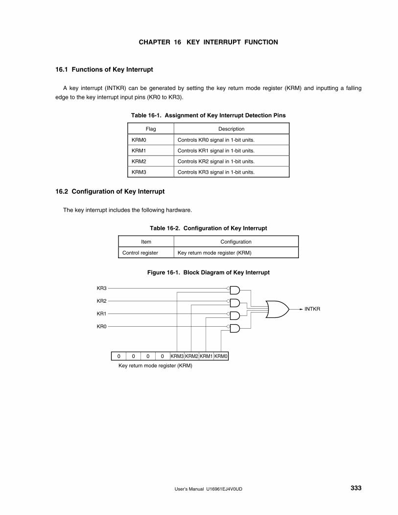
User’s Manual U16961EJ4V0UD 333
CHAPTER 16 KEY INTERRUPT FUNCTION
16.1 Functions of Key Interrupt
A key interrupt (INTKR) can be generated by setting the key return mode register (KRM) and inputting a falling
edge to the key interrupt input pins (KR0 to KR3).
Table 16-1. Assignment of Key Interrupt Detection Pins
Flag Description
KRM0 Controls KR0 signal in 1-bit units.
KRM1 Controls KR1 signal in 1-bit units.
KRM2 Controls KR2 signal in 1-bit units.
KRM3 Controls KR3 signal in 1-bit units.
16.2 Configuration of Key Interrupt
The key interrupt includes the following hardware.
Table 16-2. Configuration of Key Interrupt
Item Configuration
Control register Key return mode register (KRM)
Figure 16-1. Block Diagram of Key Interrupt
INTKR
Key return mode register (KRM)
0 0 0 0 KRM3 KRM2 KRM1 KRM0
KR3
KR2
KR1
KR0
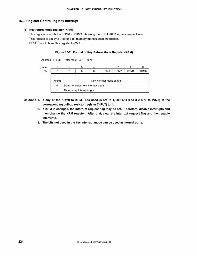
CHAPTER 16 KEY INTERRUPT FUNCTION
User’s Manual U16961EJ4V0UD 334
16.3 Register Controlling Key Interrupt
(1) Key return mode register (KRM)
This register controls the KRM0 to KRM3 bits using the KR0 to KR3 signals, respectively.
This register is set by a 1-bit or 8-bit memory manipulation instruction.
RESET input clears this register to 00H.
Figure 16-2. Format of Key Return Mode Register (KRM)
0
Does not detect key interrupt signal
Detects key interrupt signal
KRMn
0
1
Key interrupt mode control
KRM 0 0 0 KRM3 KRM2 KRM1 KRM0
Address: FF6EH After reset: 00H R/W
Symbol 7 6 5 4 3 2 0
Cautions 1. If any of the KRM0 to KRM3 bits used is set to 1, set bits 0 to 3 (PU70 to PU73) of the
corresponding pull-up resistor register 7 (PU7) to 1.
2. If KRM is changed, the interrupt request flag may be set. Therefore, disable interrupts and
then change the KRM register. After that, clear the interrupt request flag and then enable
interrupts.
3. The bits not used in the key interrupt mode can be used as normal ports.
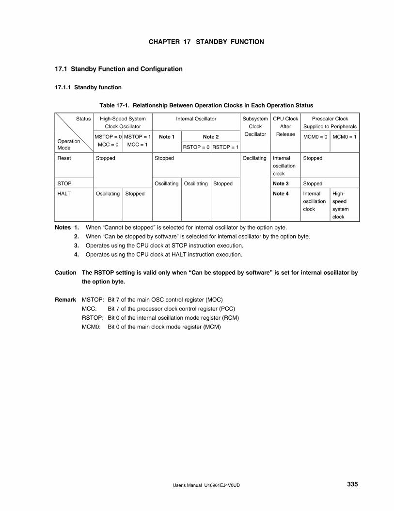
User’s Manual U16961EJ4V0UD 335
CHAPTER 17 STANDBY FUNCTION
17.1 Standby Function and Configuration
17.1.1 Standby function
Table 17-1. Relationship Between Operation Clocks in Each Operation Status
High-Speed System
Clock Oscillator
Internal Oscillator Prescaler Clock
Supplied to Peripherals
Note 2
Status
Operation Mode
MSTOP = 0
MCC = 0
MSTOP = 1
MCC = 1
Note 1
RSTOP = 0 RSTOP = 1
Subsystem
Clock
Oscillator
CPU Clock
After
Release MCM0 = 0 MCM0 = 1
Reset Stopped Internal
oscillation
clock
Stopped
STOP
Stopped
Note 3 Stopped
HALT Oscillating Stopped
Oscillating Oscillating Stopped
Oscillating
Note 4 Internal
oscillation
clock
High-
speed
system
clock
Notes 1. When “Cannot be stopped” is selected for internal oscillator by the option byte.
2. When “Can be stopped by software” is selected for internal oscillator by the option byte.
3. Operates using the CPU clock at STOP instruction execution.
4. Operates using the CPU clock at HALT instruction execution.
Caution The RSTOP setting is valid only when “Can be stopped by software” is set for internal oscillator by
the option byte.
Remark MSTOP: Bit 7 of the main OSC control register (MOC)
MCC: Bit 7 of the processor clock control register (PCC)
RSTOP: Bit 0 of the internal oscillation mode register (RCM)
MCM0: Bit 0 of the main clock mode register (MCM)
CHAPTER 17 STANDBY FUNCTION
User’s Manual U16961EJ4V0UD 336
The standby function is designed to reduce the operating current of the system. The following two modes are
available.
(1) HALT mode
HALT instruction execution sets the HALT mode. In the HALT mode, the CPU operation clock is stopped. If the
high-speed system clock oscillator, internal oscillator, or subsystem clock oscillator is operating before the HALT
mode is set, oscillation of each clock continues. In this mode, the operating current is not decreased as much as
in the STOP mode, but the HALT mode is effective for restarting operation immediately upon interrupt request
generation and carrying out intermittent operations.
(2) STOP mode
STOP instruction execution sets the STOP mode. In the STOP mode, the high-speed system clock oscillator
stops, stopping the whole system, thereby considerably reducing the CPU operating current.
Because this mode can be released by an interrupt request, it enables intermittent operations to be carried out.
However, because a wait time is required to secure the oscillation stabilization time after the STOP mode is
released, select the HALT mode if it is necessary to start processing immediately upon interrupt request
generation.
In either of these two modes, all the contents of registers, flags and data memory just before the standby mode is
set are held. The I/O port output latches and output buffer statuses are also held.
Cautions 1. STOP mode can be used only when CPU is operating on the high-speed system clock or
internal oscillation clock. HALT mode can be used when CPU is operating on the high-speed
system clock, internal oscillation clock, or subsystem clock. However, when the STOP
instruction is executed during internal oscillation clock operation, the high-speed system
clock oscillator stops, but internal oscillator does not stop.
2. When shifting to the STOP mode, be sure to stop the peripheral hardware operation before
executing STOP instruction.
3. The following sequence is recommended for operating current reduction of the A/D converter
when the standby function is used: First clear bit 7 (ADCS) of the A/D converter mode
register (ADM) to 0 to stop the A/D conversion operation, and then execute the HALT or STOP
instruction.
4. If the internal oscillator is operating before the STOP mode is set, oscillation of the internal
oscillation clock cannot be stopped in the STOP mode. However, when the internal
oscillation clock is used as the CPU clock, the CPU operation is stopped for 17/fR (s) after
STOP mode is released.
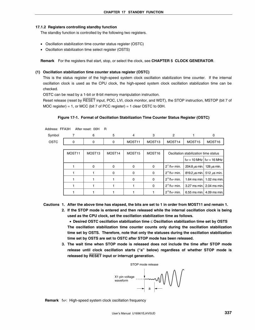
CHAPTER 17 STANDBY FUNCTION
User’s Manual U16961EJ4V0UD 337
17.1.2 Registers controlling standby function
The standby function is controlled by the following two registers.
• Oscillation stabilization time counter status register (OSTC)
• Oscillation stabilization time select register (OSTS)
Remark For the registers that start, stop, or select the clock, see CHAPTER 5 CLOCK GENERATOR.
(1) Oscillation stabilization time counter status register (OSTC)
This is the status register of the high-speed system clock oscillation stabilization time counter. If the internal
oscillation clock is used as the CPU clock, the high-speed system clock oscillation stabilization time can be
checked.
OSTC can be read by a 1-bit or 8-bit memory manipulation instruction.
Reset release (reset by RESET input, POC, LVI, clock monitor, and WDT), the STOP instruction, MSTOP (bit 7 of
MOC register) = 1, or MCC (bit 7 of PCC register) = 1 clear OSTC to 00H.
Figure 17-1. Format of Oscillation Stabilization Time Counter Status Register (OSTC)
Address: FFA3H After reset: 00H R
Symbol 7 6 5 4 3 2 1 0
OSTC 0 0 0 MOST11 MOST13 MOST14 MOST15 MOST16
MOST13 MOST14 MOST15 MOST16 Oscillation stabilization time status
MOST11
fXP = 10 MHz fXP = 16 MHz
1 0 0 0 0 211/fXP min. 204.8 µs min. 128 µs min.
1 1 0 0 0 213/fXP min. 819.2 µs min. 512 µs min.
1 1 1 0 0 214/fXP min. 1.64 ms min. 1.02 ms min.
1 1 1 1 0 215/fXP min. 3.27 ms min. 2.04 ms min.
1 1 1 1 1 216/fXP min. 6.55 ms min. 4.09 ms min.
Cautions 1. After the above time has elapsed, the bits are set to 1 in order from MOST11 and remain 1.
2. If the STOP mode is entered and then released while the internal oscillation clock is being
used as the CPU clock, set the oscillation stabilization time as follows.
• Desired OSTC oscillation stabilization time ≤ Oscillation stabilization time set by OSTS
The oscillation stabilization time counter counts only during the oscillation stabilization
time set by OSTS. Therefore, note that only the statuses during the oscillation stabilization
time set by OSTS are set to OSTC after STOP mode has been released.
3. The wait time when STOP mode is released does not include the time after STOP mode
release until clock oscillation starts (“a” below) regardless of whether STOP mode is
released by RESET input or interrupt generation.
a
STOP mode release
X1 pin voltagewaveform
Remark fXP: High-speed system clock oscillation frequency
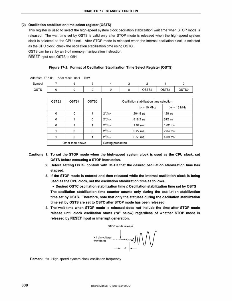
CHAPTER 17 STANDBY FUNCTION
User’s Manual U16961EJ4V0UD 338
(2) Oscillation stabilization time select register (OSTS)
This register is used to select the high-speed system clock oscillation stabilization wait time when STOP mode is
released. The wait time set by OSTS is valid only after STOP mode is released when the high-speed system
clock is selected as the CPU clock. After STOP mode is released when the internal oscillation clock is selected
as the CPU clock, check the oscillation stabilization time using OSTC.
OSTS can be set by an 8-bit memory manipulation instruction.
RESET input sets OSTS to 05H.
Figure 17-2. Format of Oscillation Stabilization Time Select Register (OSTS)
Address: FFA4H After reset: 05H R/W
Symbol 7 6 5 4 3 2 1 0
OSTS 0 0 0 0 0 OSTS2 OSTS1 OSTS0
OSTS2 OSTS1 OSTS0 Oscillation stabilization time selection
fXP = 10 MHz fXP = 16 MHz
0 0 1 211/fXP 204.8 µs 128 µs
0 1 0 213/fXP 819.2 µs 512 µs
0 1 1 214/fXP 1.64 ms 1.02 ms
1 0 0 215/fXP 3.27 ms 2.04 ms
1 0 1 216/fXP 6.55 ms 4.09 ms
Other than above Setting prohibited
Cautions 1. To set the STOP mode when the high-speed system clock is used as the CPU clock, set
OSTS before executing a STOP instruction.
2. Before setting OSTS, confirm with OSTC that the desired oscillation stabilization time has
elapsed.
3. If the STOP mode is entered and then released while the internal oscillation clock is being
used as the CPU clock, set the oscillation stabilization time as follows.
• Desired OSTC oscillation stabilization time ≤ Oscillation stabilization time set by OSTS
The oscillation stabilization time counter counts only during the oscillation stabilization
time set by OSTS. Therefore, note that only the statuses during the oscillation stabilization
time set by OSTS are set to OSTC after STOP mode has been released.
4. The wait time when STOP mode is released does not include the time after STOP mode
release until clock oscillation starts (“a” below) regardless of whether STOP mode is
released by RESET input or interrupt generation.
a
STOP mode release
X1 pin voltagewaveform
Remark fXP: High-speed system clock oscillation frequency
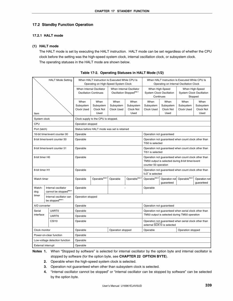
CHAPTER 17 STANDBY FUNCTION
User’s Manual U16961EJ4V0UD 339
17.2 Standby Function Operation
17.2.1 HALT mode
(1) HALT mode
The HALT mode is set by executing the HALT instruction. HALT mode can be set regardless of whether the CPU
clock before the setting was the high-speed system clock, internal oscillation clock, or subsystem clock.
The operating statuses in the HALT mode are shown below.
Table 17-2. Operating Statuses in HALT Mode (1/2)
When HALT Instruction Is Executed While CPU Is Operating on High-Speed System Clock
When HALT Instruction Is Executed While CPU Is Operating on Internal Oscillation Clock
When Internal Oscillator Oscillation Continues
When Internal Oscillator Oscillation StoppedNote 1
When High-Speed System Clock Oscillation
Continues
When High-Speed System Clock Oscillation
Stopped
HALT Mode Setting
Item
When Subsystem Clock Used
When Subsystem Clock Not
Used
When Subsystem Clock Used
When Subsystem Clock Not
Used
When Subsystem Clock Used
When Subsystem Clock Not
Used
When Subsystem Clock Used
When Subsystem Clock Not
Used
System clock Clock supply to the CPU is stopped.
CPU Operation stopped
Port (latch) Status before HALT mode was set is retained
16-bit timer/event counter 00 Operable Operation not guaranteed
8-bit timer/event counter 50 Operable Operation not guaranteed when count clock other than TI50 is selected
8-bit timer/event counter 51 Operable Operation not guaranteed when count clock other than TI51 is selected
8-bit timer H0 Operable Operation not guaranteed when count clock other than TM50 output is selected during 8-bit timer/event counter 50 operation
8-bit timer H1 Operable Operation not guaranteed when count clock other than fR/27 is selected
Watch timer Operable OperableNote 2 Operable OperableNote 2 OperableNote 3 Operation not guaranteed
OperableNote 3 Operation not guaranteed
Internal oscillator cannot be stoppedNote 4
Operable − Operable Watch-dog timer Internal oscillator can
be stoppedNote 4 Operation stopped
A/D converter Operable Operation not guaranteed
UART0 Operable
UART6 Operable
Operation not guaranteed when serial clock other than TM50 output is selected during TM50 operation
Serial interface
CSI10 Operable Operation not guaranteed when serial clock other than external SCK10 is selected
Clock monitor Operable Operation stopped Operable Operation stopped
Power-on-clear function Operable
Low-voltage detection function Operable
External interrupt Operable
Notes 1. When “Stopped by software” is selected for internal oscillator by the option byte and internal oscillator is
stopped by software (for the option byte, see CHAPTER 22 OPTION BYTE).
2. Operable when the high-speed system clock is selected.
3. Operation not guaranteed when other than subsystem clock is selected.
4. “Internal oscillator cannot be stopped” or “internal oscillator can be stopped by software” can be selected
by the option byte.
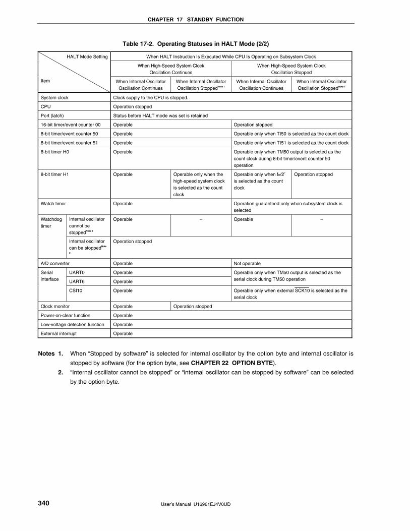
CHAPTER 17 STANDBY FUNCTION
User’s Manual U16961EJ4V0UD 340
Table 17-2. Operating Statuses in HALT Mode (2/2)
When HALT Instruction Is Executed While CPU Is Operating on Subsystem Clock
When High-Speed System Clock Oscillation Continues
When High-Speed System Clock Oscillation Stopped
HALT Mode Setting
Item When Internal Oscillator Oscillation Continues
When Internal Oscillator Oscillation StoppedNote 1
When Internal Oscillator Oscillation Continues
When Internal Oscillator Oscillation StoppedNote 1
System clock Clock supply to the CPU is stopped.
CPU Operation stopped
Port (latch) Status before HALT mode was set is retained
16-bit timer/event counter 00 Operable Operation stopped
8-bit timer/event counter 50 Operable Operable only when TI50 is selected as the count clock
8-bit timer/event counter 51 Operable Operable only when TI51 is selected as the count clock
8-bit timer H0 Operable Operable only when TM50 output is selected as the count clock during 8-bit timer/event counter 50 operation
8-bit timer H1 Operable Operable only when the high-speed system clock is selected as the count clock
Operable only when fR/27 is selected as the count clock
Operation stopped
Watch timer Operable Operation guaranteed only when subsystem clock is selected
Internal oscillator cannot be stoppedNote 2
Operable − Operable − Watchdog timer
Internal oscillator can be stoppedNote
2
Operation stopped
A/D converter Operable Not operable
UART0 Operable
UART6 Operable
Operable only when TM50 output is selected as the serial clock during TM50 operation
Serial interface
CSI10 Operable Operable only when external SCK10 is selected as the serial clock
Clock monitor Operable Operation stopped
Power-on-clear function Operable
Low-voltage detection function Operable
External interrupt Operable
Notes 1. When “Stopped by software” is selected for internal oscillator by the option byte and internal oscillator is
stopped by software (for the option byte, see CHAPTER 22 OPTION BYTE).
2. “Internal oscillator cannot be stopped” or “internal oscillator can be stopped by software” can be selected
by the option byte.
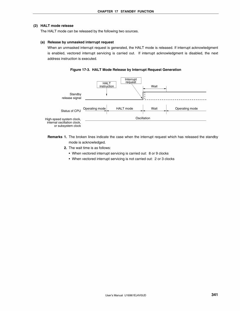
CHAPTER 17 STANDBY FUNCTION
User’s Manual U16961EJ4V0UD 341
(2) HALT mode release
The HALT mode can be released by the following two sources.
(a) Release by unmasked interrupt request
When an unmasked interrupt request is generated, the HALT mode is released. If interrupt acknowledgment
is enabled, vectored interrupt servicing is carried out. If interrupt acknowledgment is disabled, the next
address instruction is executed.
Figure 17-3. HALT Mode Release by Interrupt Request Generation
HALTinstruction Wait
Wait Operating modeHALT modeOperating mode
OscillationHigh-speed system clock,internal oscillation clock,
or subsystem clock
Status of CPU
Standbyrelease signal
Interruptrequest
Remarks 1. The broken lines indicate the case when the interrupt request which has released the standby
mode is acknowledged.
2. The wait time is as follows:
• When vectored interrupt servicing is carried out: 8 or 9 clocks
• When vectored interrupt servicing is not carried out: 2 or 3 clocks
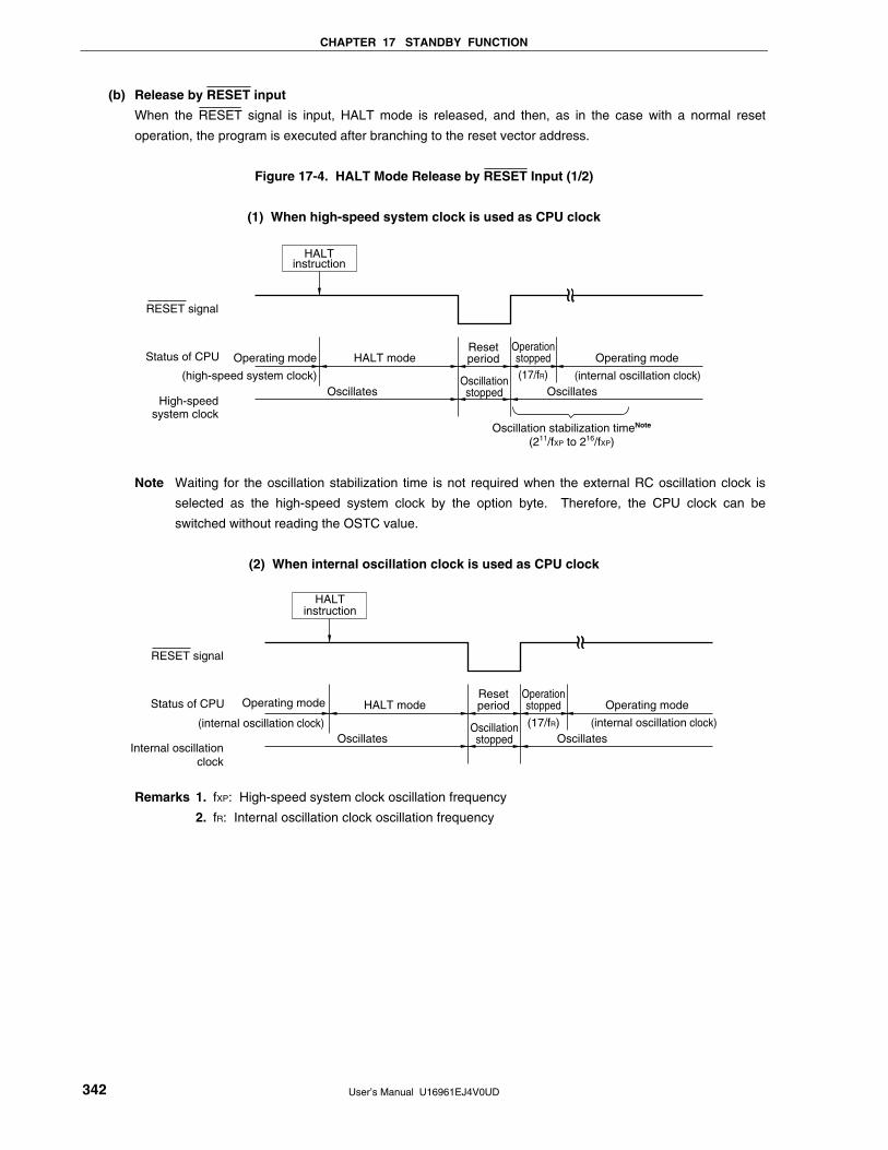
CHAPTER 17 STANDBY FUNCTION
User’s Manual U16961EJ4V0UD 342
(b) Release by RESET input
When the RESET signal is input, HALT mode is released, and then, as in the case with a normal reset
operation, the program is executed after branching to the reset vector address.
Figure 17-4. HALT Mode Release by RESET Input (1/2)
(1) When high-speed system clock is used as CPU clock
HALT
instruction
RESET signal
High-speedsystem clock
Operating mode HALT modeResetperiod
Operationstopped Operating mode
OscillatesOscillationstopped Oscillates
Status of CPU
(high-speed system clock)
Oscillation stabilization timeNote
(211/fXP to 216/fXP)
(internal oscillation clock)(17/fR)
Note Waiting for the oscillation stabilization time is not required when the external RC oscillation clock is
selected as the high-speed system clock by the option byte. Therefore, the CPU clock can be
switched without reading the OSTC value.
(2) When internal oscillation clock is used as CPU clock
HALT
instruction
RESET signal
Internal oscillation clock
Operating mode HALT modeResetperiod
Operationstopped Operating mode
OscillatesOscillationstopped Oscillates
Status of CPU
(internal oscillation clock)(17/fR)(internal oscillation clock)
Remarks 1. fXP: High-speed system clock oscillation frequency
2. fR: Internal oscillation clock oscillation frequency

CHAPTER 17 STANDBY FUNCTION
User’s Manual U16961EJ4V0UD 343
Figure 17-4. HALT Mode Release by RESET Input (2/2)
(3) When subsystem clock is used as CPU clock
HALT instruction
RESET signal
Subsystem clock
Operatingmode HALT mode
Resetperiod
Operationstopped Operating mode
Oscillates
Status of CPU
(internal oscillation clock)(17/fR)Subsystemclock
Remark fR: Internal oscillation clock oscillation frequency
Table 17-3. Operation in Response to Interrupt Request in HALT Mode
Release Source MK×× PR×× IE ISP Operation
0 0 0 × Next address
instruction execution
0 0 1 × Interrupt servicing
execution
0 1 0 1
0 1 × 0
Next address
instruction execution
0 1 1 1 Interrupt servicing
execution
Maskable interrupt
request
1 × × × HALT mode held
RESET input − − × × Reset processing
×: Don’t care
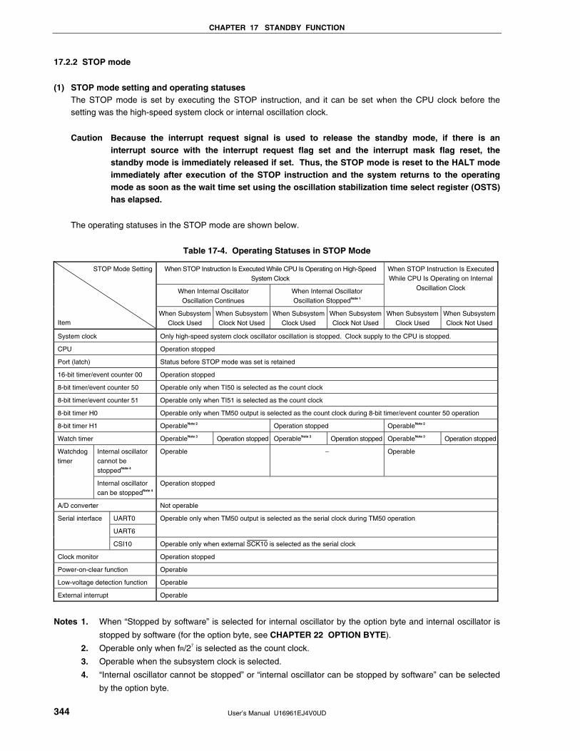
CHAPTER 17 STANDBY FUNCTION
User’s Manual U16961EJ4V0UD 344
17.2.2 STOP mode
(1) STOP mode setting and operating statuses The STOP mode is set by executing the STOP instruction, and it can be set when the CPU clock before the
setting was the high-speed system clock or internal oscillation clock.
Caution Because the interrupt request signal is used to release the standby mode, if there is an
interrupt source with the interrupt request flag set and the interrupt mask flag reset, the standby mode is immediately released if set. Thus, the STOP mode is reset to the HALT mode immediately after execution of the STOP instruction and the system returns to the operating mode as soon as the wait time set using the oscillation stabilization time select register (OSTS) has elapsed.
The operating statuses in the STOP mode are shown below.
Table 17-4. Operating Statuses in STOP Mode
When STOP Instruction Is Executed While CPU Is Operating on High-Speed System Clock
When Internal Oscillator Oscillation Continues
When Internal Oscillator Oscillation StoppedNote 1
When STOP Instruction Is Executed While CPU Is Operating on Internal
Oscillation Clock
STOP Mode Setting
Item When Subsystem
Clock Used When Subsystem Clock Not Used
When Subsystem Clock Used
When Subsystem Clock Not Used
When Subsystem Clock Used
When Subsystem Clock Not Used
System clock Only high-speed system clock oscillator oscillation is stopped. Clock supply to the CPU is stopped.
CPU Operation stopped
Port (latch) Status before STOP mode was set is retained
16-bit timer/event counter 00 Operation stopped
8-bit timer/event counter 50 Operable only when TI50 is selected as the count clock
8-bit timer/event counter 51 Operable only when TI51 is selected as the count clock
8-bit timer H0 Operable only when TM50 output is selected as the count clock during 8-bit timer/event counter 50 operation
8-bit timer H1 OperableNote 2 Operation stopped OperableNote 2
Watch timer OperableNote 3 Operation stopped OperableNote 3 Operation stopped OperableNote 3 Operation stopped
Internal oscillator cannot be stoppedNote 4
Operable − Operable Watchdog timer
Internal oscillator can be stoppedNote 4
Operation stopped
A/D converter Not operable
UART0
UART6
Operable only when TM50 output is selected as the serial clock during TM50 operation Serial interface
CSI10 Operable only when external SCK10 is selected as the serial clock
Clock monitor Operation stopped
Power-on-clear function Operable
Low-voltage detection function Operable
External interrupt Operable
Notes 1. When “Stopped by software” is selected for internal oscillator by the option byte and internal oscillator is
stopped by software (for the option byte, see CHAPTER 22 OPTION BYTE).
2. Operable only when fR/27 is selected as the count clock.
3. Operable when the subsystem clock is selected.
4. “Internal oscillator cannot be stopped” or “internal oscillator can be stopped by software” can be selected
by the option byte.
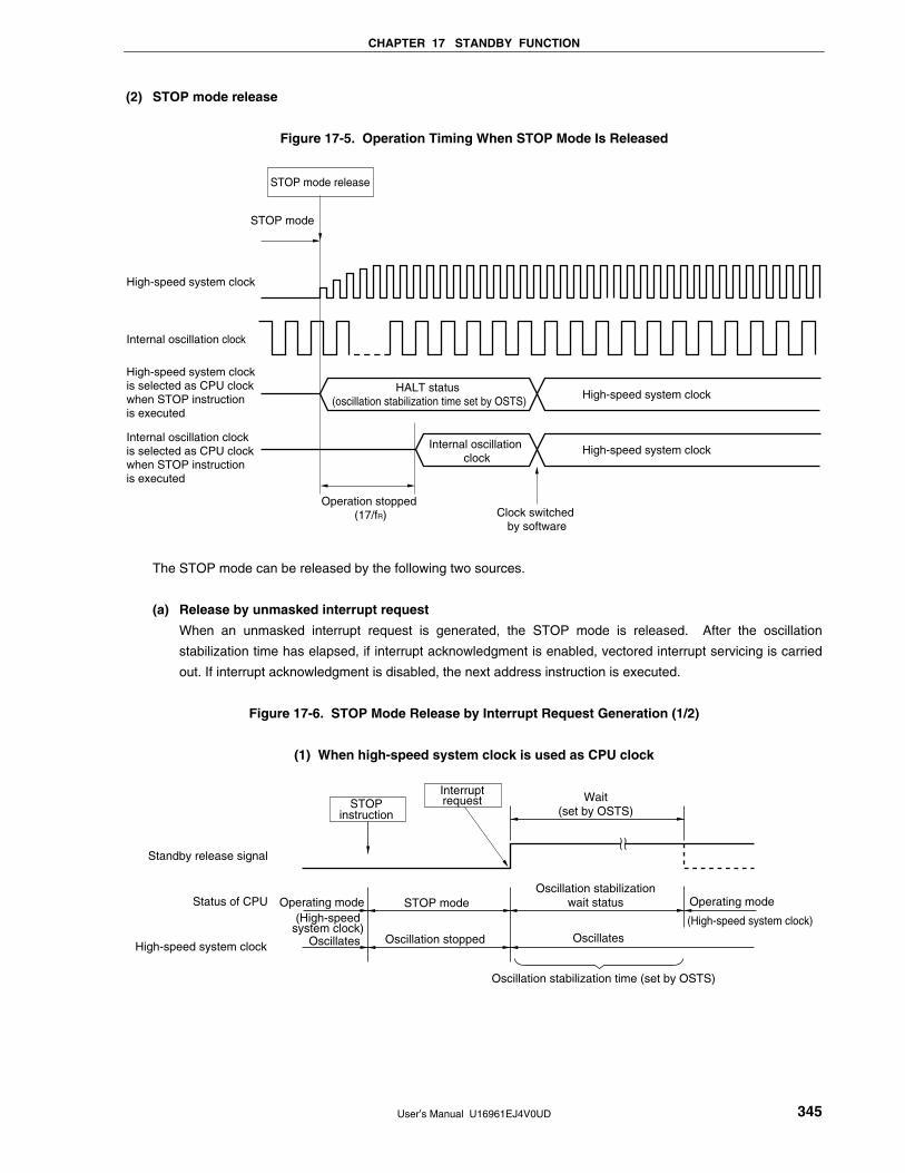
CHAPTER 17 STANDBY FUNCTION
User’s Manual U16961EJ4V0UD 345
(2) STOP mode release
Figure 17-5. Operation Timing When STOP Mode Is Released
Internal oscillation clock is selected as CPU clock when STOP instruction is executed
Internal oscillation clock
High-speed system clock
High-speed system clockis selected as CPU clock when STOP instruction is executed
STOP mode release
STOP mode
Operation stopped (17/fR) Clock switched
by software
Internal oscillation clock
High-speed system clock
HALT status (oscillation stabilization time set by OSTS)
High-speed system clock
The STOP mode can be released by the following two sources.
(a) Release by unmasked interrupt request
When an unmasked interrupt request is generated, the STOP mode is released. After the oscillation
stabilization time has elapsed, if interrupt acknowledgment is enabled, vectored interrupt servicing is carried
out. If interrupt acknowledgment is disabled, the next address instruction is executed.
Figure 17-6. STOP Mode Release by Interrupt Request Generation (1/2)
(1) When high-speed system clock is used as CPU clock
Operating mode Operating mode
OscillatesOscillates
STOPinstruction
STOP mode
Wait(set by OSTS)
Standby release signal
Oscillation stabilizationwait status
Oscillation stoppedHigh-speed system clock
Status of CPU
Oscillation stabilization time (set by OSTS)
(High-speed system clock)(High-speedsystem clock)
Interruptrequest
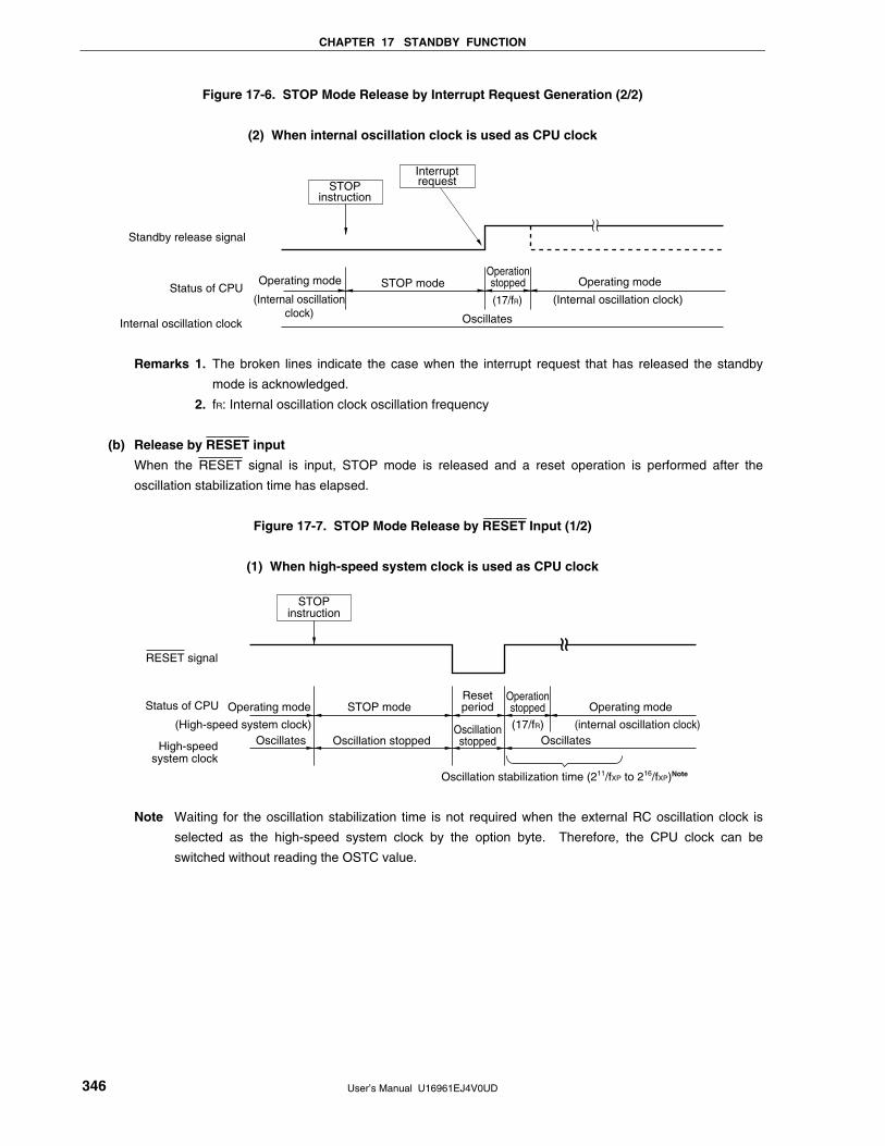
CHAPTER 17 STANDBY FUNCTION
User’s Manual U16961EJ4V0UD 346
Figure 17-6. STOP Mode Release by Interrupt Request Generation (2/2)
(2) When internal oscillation clock is used as CPU clock
Operating mode Operating mode
Oscillates
STOPinstruction
STOP mode
Standby release signal
Internal oscillation clock
Status of CPU(Internal oscillation
clock)
Operationstopped
(17/fR) (Internal oscillation clock)
Interruptrequest
Remarks 1. The broken lines indicate the case when the interrupt request that has released the standby
mode is acknowledged.
2. fR: Internal oscillation clock oscillation frequency
(b) Release by RESET input
When the RESET signal is input, STOP mode is released and a reset operation is performed after the
oscillation stabilization time has elapsed.
Figure 17-7. STOP Mode Release by RESET Input (1/2)
(1) When high-speed system clock is used as CPU clock
STOP
instruction
RESET signal
High-speedsystem clock
Operating mode STOP modeResetperiod
Operationstopped Operating mode
OscillatesOscillationstopped Oscillates
Status of CPU
(High-speed system clock)
Oscillation stabilization time (211/fXP to 216/fXP)Note
(internal oscillation clock)(17/fR)Oscillation stopped
Note Waiting for the oscillation stabilization time is not required when the external RC oscillation clock is
selected as the high-speed system clock by the option byte. Therefore, the CPU clock can be
switched without reading the OSTC value.
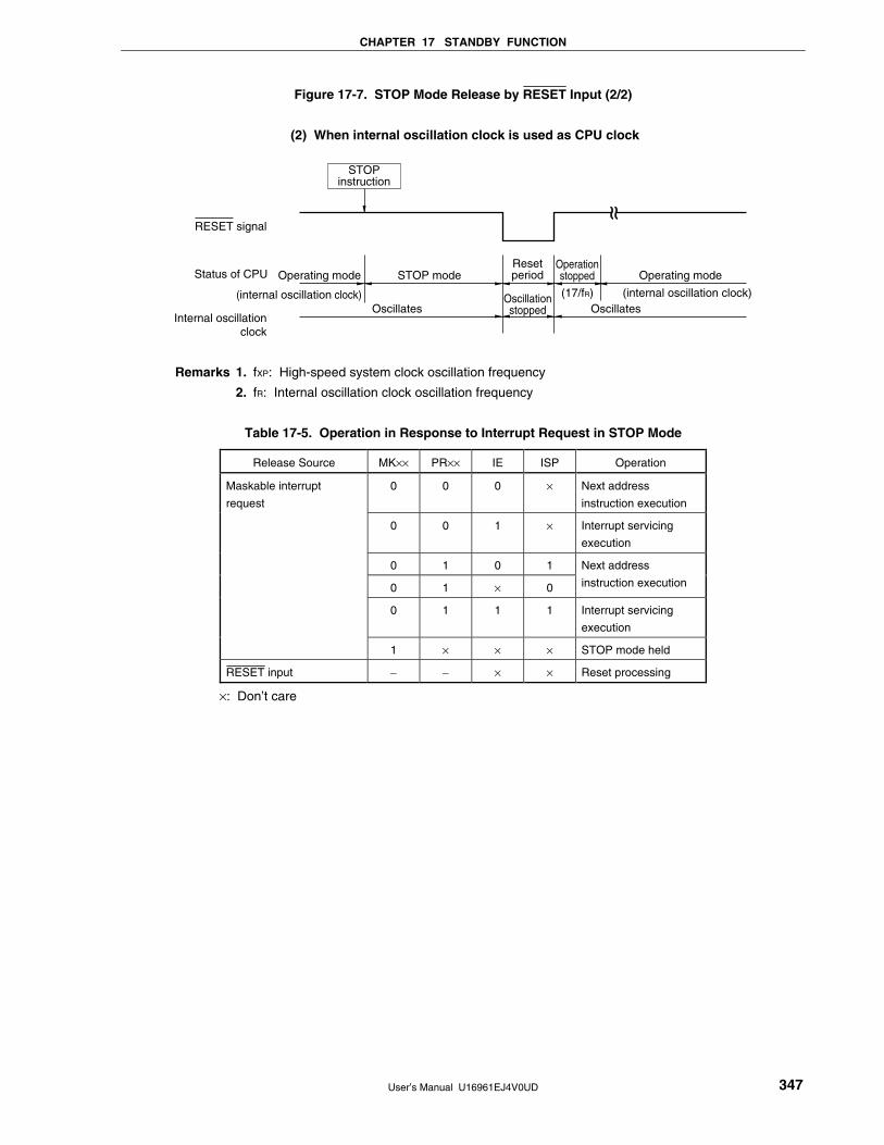
CHAPTER 17 STANDBY FUNCTION
User’s Manual U16961EJ4V0UD 347
Figure 17-7. STOP Mode Release by RESET Input (2/2)
(2) When internal oscillation clock is used as CPU clock
STOP
instruction
RESET signal
Internal oscillation clock
Operating mode STOP modeResetperiod
Operationstopped Operating mode
OscillatesOscillationstopped Oscillates
Status of CPU
(internal oscillation clock)(17/fR)(internal oscillation clock)
Remarks 1. fXP: High-speed system clock oscillation frequency
2. fR: Internal oscillation clock oscillation frequency
Table 17-5. Operation in Response to Interrupt Request in STOP Mode
Release Source MK×× PR×× IE ISP Operation
0 0 0 × Next address
instruction execution
0 0 1 × Interrupt servicing
execution
0 1 0 1
0 1 × 0
Next address
instruction execution
0 1 1 1 Interrupt servicing
execution
Maskable interrupt
request
1 × × × STOP mode held
RESET input − − × × Reset processing
×: Don’t care
User’s Manual U16961EJ4V0UD 348
CHAPTER 18 RESET FUNCTION
The following five operations are available to generate a reset signal.
(1) External reset input via RESET pin
(2) Internal reset by watchdog timer program loop detection
(3) Internal reset by clock monitor high-speed system clock oscillation stop detection
(4) Internal reset by comparison of supply voltage and detection voltage of power-on-clear (POC) circuit
(5) Internal reset by comparison of supply voltage and detection voltage of low-power-supply detector (LVI)
External and internal resets have no functional differences. In both cases, program execution starts at the address
at 0000H and 0001H when the reset signal is input.
A reset is applied when a low level is input to the RESET pin, the watchdog timer overflows, high-speed system
clock oscillation stop is detected by the clock monitor, or by POC and LVI circuit voltage detection, and each item of
hardware is set to the status shown in Table 18-1. Each pin is high impedance during reset input or during the
oscillation stabilization time just after reset release, except for P130, which is low-level output.
When a high level is input to the RESET pin, the reset is released and program execution starts using the internal
oscillation clock after the CPU clock operation has stopped for 17/fR (s). A reset generated by the watchdog timer and
clock monitor sources is automatically released after the reset, and program execution starts using the internal
oscillation clock after the CPU clock operation has stopped for 17/fR (s) (see Figures 18-2 to 18-4). Reset by POC
and LVI circuit power supply detection is automatically released when VDD > VPOC or VDD > VLVI after the reset, and
program execution starts using the internal oscillation clock after the CPU clock operation has stopped for 17/fR (s)
(see CHAPTER 20 POWER-ON-CLEAR CIRCUIT and CHAPTER 21 LOW-VOLTAGE DETECTOR).
Cautions 1. For an external reset, input a low level for 10 µs or more to the RESET pin.
2. During reset input, the high-speed system clock and internal oscillation clock stop
oscillating.
3. When the STOP mode is released by a reset, the STOP mode contents are held during reset
input. However, the port pins become high-impedance, except for P130, which is set to low-
level output.
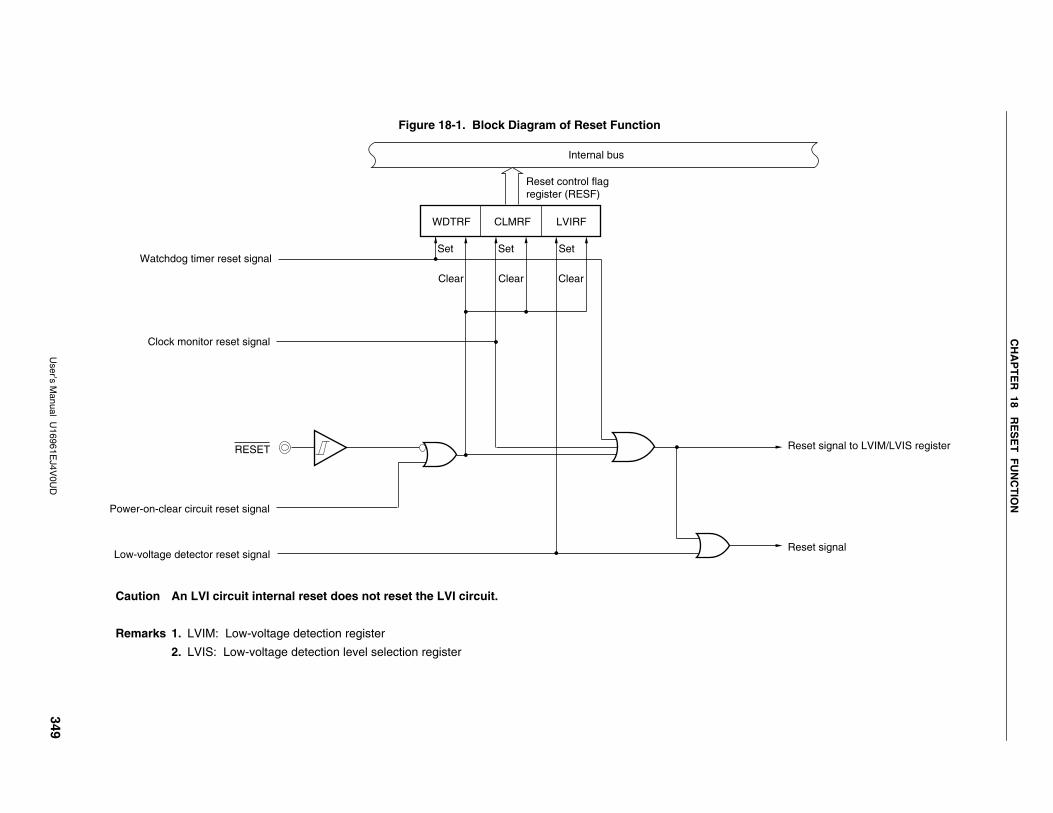
CH
AP
TE
R 18 R
ES
ET
FU
NC
TIO
N
User’s M
anual U16961E
J4V0U
D
349
Figure 18-1. Block Diagram of Reset Function
CLMRF LVIRFWDTRF
RESET
Reset control flag register (RESF)
Internal bus
Watchdog timer reset signal
Clock monitor reset signal
Power-on-clear circuit reset signal
Low-voltage detector reset signalReset signal
Reset signal to LVIM/LVIS register
Clear
SetSet
Clear Clear
Set
Caution An LVI circuit internal reset does not reset the LVI circuit.
Remarks 1. LVIM: Low-voltage detection register
2. LVIS: Low-voltage detection level selection register
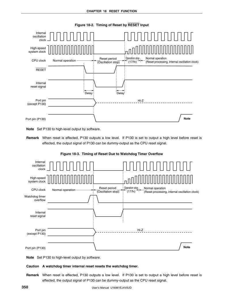
CHAPTER 18 RESET FUNCTION
User’s Manual U16961EJ4V0UD 350
Figure 18-2. Timing of Reset by RESET Input
Delay Delay
Hi-Z
Normal operationCPU clockReset period
(Oscillation stop)Operation stop
(17/fR)Normal operation (Reset processing, internal oscillation clock)
RESET
Internalreset signal
Port pin(except P130)
High-speedsystem clock
Internal oscillation
clock
Port pin (P130) Note
Note Set P130 to high-level output by software.
Remark When reset is effected, P130 outputs a low level. If P130 is set to output a high level before reset is
effected, the output signal of P130 can be dummy-output as the CPU reset signal.
Figure 18-3. Timing of Reset Due to Watchdog Timer Overflow
Hi-Z
Normal operationReset period
(Oscillation stop)CPU clock
Watchdog timeroverflow
Internalreset signal
Port pin(except P130)
Operation stop(17/fR)
Normal operation (Reset processing, internal oscillation clock)
High-speedsystem clock
Internal oscillation
clock
Note Port pin (P130)
Note Set P130 to high-level output by software.
Caution A watchdog timer internal reset resets the watchdog timer.
Remark When reset is effected, P130 outputs a low level. If P130 is set to output a high level before reset is
effected, the output signal of P130 can be dummy-output as the CPU reset signal.
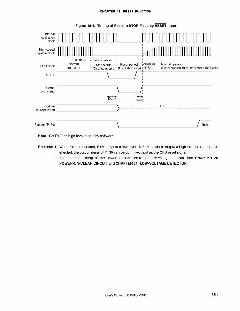
CHAPTER 18 RESET FUNCTION
User’s Manual U16961EJ4V0UD 351
Figure 18-4. Timing of Reset in STOP Mode by RESET Input
Delay Delay
Hi-Z
NormaloperationCPU clock Reset period
(Oscillation stop)
RESET
Internalreset signal
Port pin(except P130)
STOP instruction execution
Stop status (Oscillation stop)
Operation stop(17/fR)
Normal operation (Reset processing, internal oscillation clock)
High-speedsystem clock
Internal oscillation
clock
Port pin (P130) Note
Note Set P130 to high-level output by software.
Remarks 1. When reset is effected, P130 outputs a low level. If P130 is set to output a high level before reset is
effected, the output signal of P130 can be dummy-output as the CPU reset signal.
2. For the reset timing of the power-on-clear circuit and low-voltage detector, see CHAPTER 20
POWER-ON-CLEAR CIRCUIT and CHAPTER 21 LOW-VOLTAGE DETECTOR.
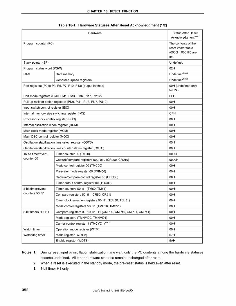
CHAPTER 18 RESET FUNCTION
User’s Manual U16961EJ4V0UD 352
Table 18-1. Hardware Statuses After Reset Acknowledgment (1/2)
Hardware Status After Reset
AcknowledgmentNote 1
Program counter (PC) The contents of the reset vector table (0000H, 0001H) are
set.
Stack pointer (SP) Undefined
Program status word (PSW) 02H
Data memory UndefinedNote 2 RAM
General-purpose registers UndefinedNote 2
Port registers (P0 to P3, P6, P7, P12, P13) (output latches) 00H (undefined only for P2)
Port mode registers (PM0, PM1, PM3, PM6, PM7, PM12) FFH
Pull-up resistor option registers (PU0, PU1, PU3, PU7, PU12) 00H
Input switch control register (ISC) 00H
Internal memory size switching register (IMS) CFH
Processor clock control register (PCC) 00H
Internal oscillation mode register (RCM) 00H
Main clock mode register (MCM) 00H
Main OSC control register (MOC) 00H
Oscillation stabilization time select register (OSTS) 05H
Oscillation stabilization time counter status register (OSTC) 00H
Timer counter 00 (TM00) 0000H
Capture/compare registers 000, 010 (CR000, CR010) 0000H
Mode control register 00 (TMC00) 00H
Prescaler mode register 00 (PRM00) 00H
Capture/compare control register 00 (CRC00) 00H
16-bit timer/event
counter 00
Timer output control register 00 (TOC00) 00H
Timer counters 50, 51 (TM50, TM51) 00H
Compare registers 50, 51 (CR50, CR51) 00H
Timer clock selection registers 50, 51 (TCL50, TCL51) 00H
8-bit timer/event
counters 50, 51
Mode control registers 50, 51 (TMC50, TMC51) 00H
Compare registers 00, 10, 01, 11 (CMP00, CMP10, CMP01, CMP11) 00H
Mode registers (TMHMD0, TMHMD1) 00H
8-bit timers H0, H1
Carrier control register 1 (TMCYC1)Note 3 00H
Watch timer Operation mode register (WTM) 00H
Mode register (WDTM) 67H Watchdog timer
Enable register (WDTE) 9AH
Notes 1. During reset input or oscillation stabilization time wait, only the PC contents among the hardware statuses
become undefined. All other hardware statuses remain unchanged after reset.
2. When a reset is executed in the standby mode, the pre-reset status is held even after reset.
3. 8-bit timer H1 only.
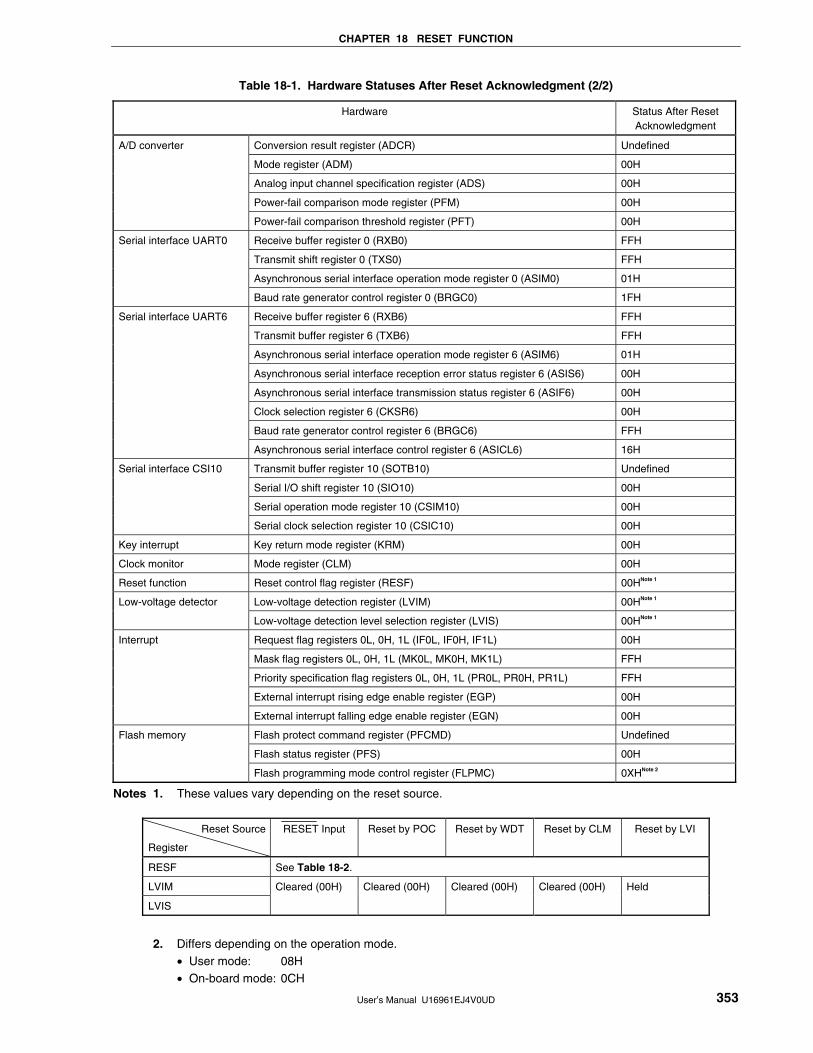
CHAPTER 18 RESET FUNCTION
User’s Manual U16961EJ4V0UD 353
Table 18-1. Hardware Statuses After Reset Acknowledgment (2/2)
Hardware Status After Reset Acknowledgment
Conversion result register (ADCR) Undefined
Mode register (ADM) 00H
Analog input channel specification register (ADS) 00H
Power-fail comparison mode register (PFM) 00H
A/D converter
Power-fail comparison threshold register (PFT) 00H
Receive buffer register 0 (RXB0) FFH
Transmit shift register 0 (TXS0) FFH
Asynchronous serial interface operation mode register 0 (ASIM0) 01H
Serial interface UART0
Baud rate generator control register 0 (BRGC0) 1FH
Receive buffer register 6 (RXB6) FFH
Transmit buffer register 6 (TXB6) FFH
Asynchronous serial interface operation mode register 6 (ASIM6) 01H
Asynchronous serial interface reception error status register 6 (ASIS6) 00H
Asynchronous serial interface transmission status register 6 (ASIF6) 00H
Clock selection register 6 (CKSR6) 00H
Baud rate generator control register 6 (BRGC6) FFH
Serial interface UART6
Asynchronous serial interface control register 6 (ASICL6) 16H
Transmit buffer register 10 (SOTB10) Undefined
Serial I/O shift register 10 (SIO10) 00H
Serial operation mode register 10 (CSIM10) 00H
Serial interface CSI10
Serial clock selection register 10 (CSIC10) 00H
Key interrupt Key return mode register (KRM) 00H
Clock monitor Mode register (CLM) 00H
Reset function Reset control flag register (RESF) 00HNote 1
Low-voltage detection register (LVIM) 00HNote 1 Low-voltage detector
Low-voltage detection level selection register (LVIS) 00HNote 1
Request flag registers 0L, 0H, 1L (IF0L, IF0H, IF1L) 00H
Mask flag registers 0L, 0H, 1L (MK0L, MK0H, MK1L) FFH
Priority specification flag registers 0L, 0H, 1L (PR0L, PR0H, PR1L) FFH
External interrupt rising edge enable register (EGP) 00H
Interrupt
External interrupt falling edge enable register (EGN) 00H
Flash protect command register (PFCMD) Undefined
Flash status register (PFS) 00H
Flash memory
Flash programming mode control register (FLPMC) 0XHNote 2
Notes 1. These values vary depending on the reset source.
Reset Source
Register
RESET Input Reset by POC Reset by WDT Reset by CLM Reset by LVI
RESF See Table 18-2.
LVIM
LVIS
Cleared (00H) Cleared (00H) Cleared (00H) Cleared (00H) Held
2. Differs depending on the operation mode.
• User mode: 08H • On-board mode: 0CH
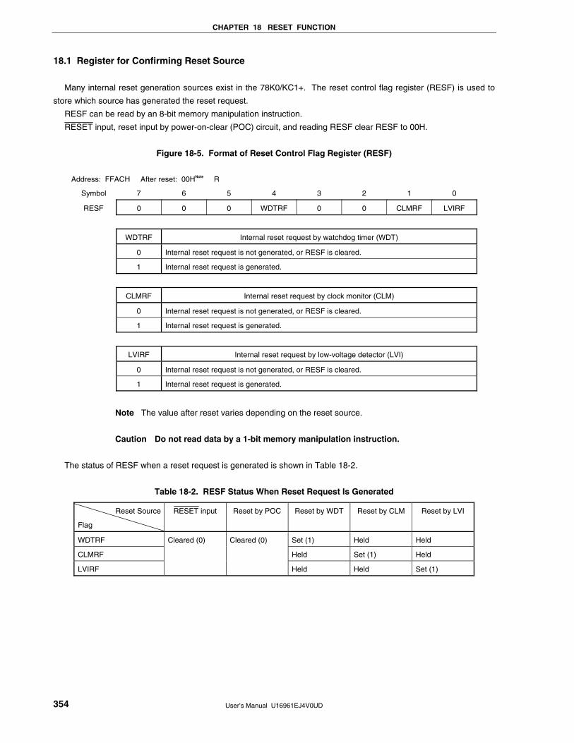
CHAPTER 18 RESET FUNCTION
User’s Manual U16961EJ4V0UD 354
18.1 Register for Confirming Reset Source
Many internal reset generation sources exist in the 78K0/KC1+. The reset control flag register (RESF) is used to
store which source has generated the reset request.
RESF can be read by an 8-bit memory manipulation instruction.
RESET input, reset input by power-on-clear (POC) circuit, and reading RESF clear RESF to 00H.
Figure 18-5. Format of Reset Control Flag Register (RESF)
Address: FFACH After reset: 00HNote R
Symbol 7 6 5 4 3 2 1 0
RESF 0 0 0 WDTRF 0 0 CLMRF LVIRF
WDTRF Internal reset request by watchdog timer (WDT)
0 Internal reset request is not generated, or RESF is cleared.
1 Internal reset request is generated.
CLMRF Internal reset request by clock monitor (CLM)
0 Internal reset request is not generated, or RESF is cleared.
1 Internal reset request is generated.
LVIRF Internal reset request by low-voltage detector (LVI)
0 Internal reset request is not generated, or RESF is cleared.
1 Internal reset request is generated.
Note The value after reset varies depending on the reset source.
Caution Do not read data by a 1-bit memory manipulation instruction.
The status of RESF when a reset request is generated is shown in Table 18-2.
Table 18-2. RESF Status When Reset Request Is Generated
Reset Source
Flag
RESET input Reset by POC Reset by WDT Reset by CLM Reset by LVI
WDTRF Set (1) Held Held
CLMRF Held Set (1) Held
LVIRF
Cleared (0) Cleared (0)
Held Held Set (1)
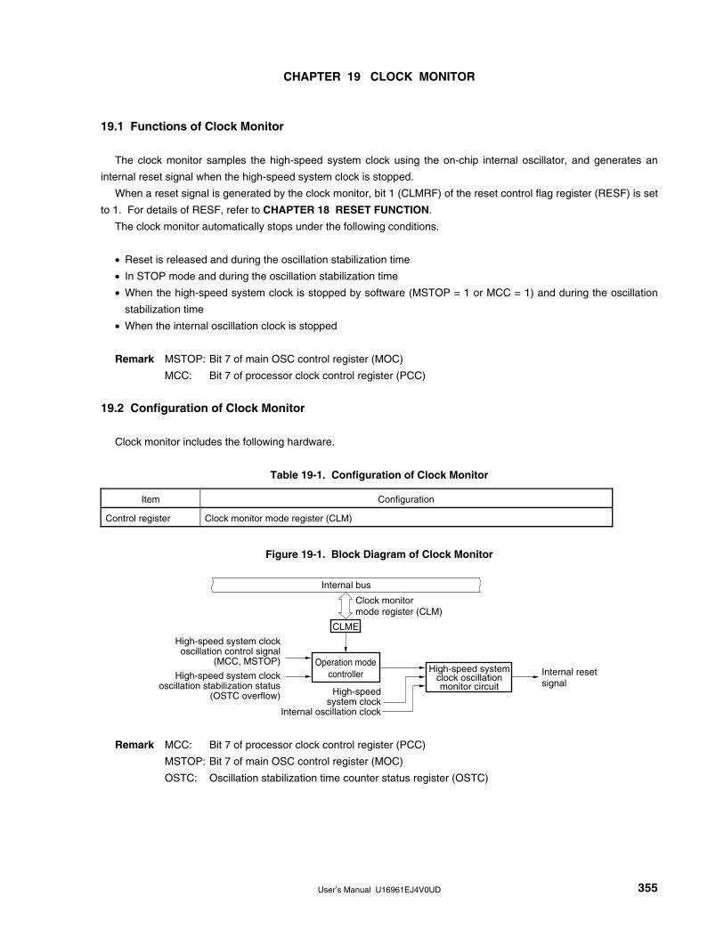
User’s Manual U16961EJ4V0UD 355
CHAPTER 19 CLOCK MONITOR
19.1 Functions of Clock Monitor
The clock monitor samples the high-speed system clock using the on-chip internal oscillator, and generates an
internal reset signal when the high-speed system clock is stopped.
When a reset signal is generated by the clock monitor, bit 1 (CLMRF) of the reset control flag register (RESF) is set
to 1. For details of RESF, refer to CHAPTER 18 RESET FUNCTION.
The clock monitor automatically stops under the following conditions.
• Reset is released and during the oscillation stabilization time
• In STOP mode and during the oscillation stabilization time
• When the high-speed system clock is stopped by software (MSTOP = 1 or MCC = 1) and during the oscillation
stabilization time
• When the internal oscillation clock is stopped
Remark MSTOP: Bit 7 of main OSC control register (MOC)
MCC: Bit 7 of processor clock control register (PCC)
19.2 Configuration of Clock Monitor
Clock monitor includes the following hardware.
Table 19-1. Configuration of Clock Monitor
Item Configuration
Control register Clock monitor mode register (CLM)
Figure 19-1. Block Diagram of Clock Monitor
Operation modecontroller
High-speedsystem clock
Internal oscillation clock
CLME
Clock monitor mode register (CLM)
Internal bus
High-speed systemclock oscillationmonitor circuit
Internal reset signal
High-speed system clockoscillation control signal
(MCC, MSTOP)
High-speed system clockoscillation stabilization status
(OSTC overflow)
Remark MCC: Bit 7 of processor clock control register (PCC)
MSTOP: Bit 7 of main OSC control register (MOC)
OSTC: Oscillation stabilization time counter status register (OSTC)
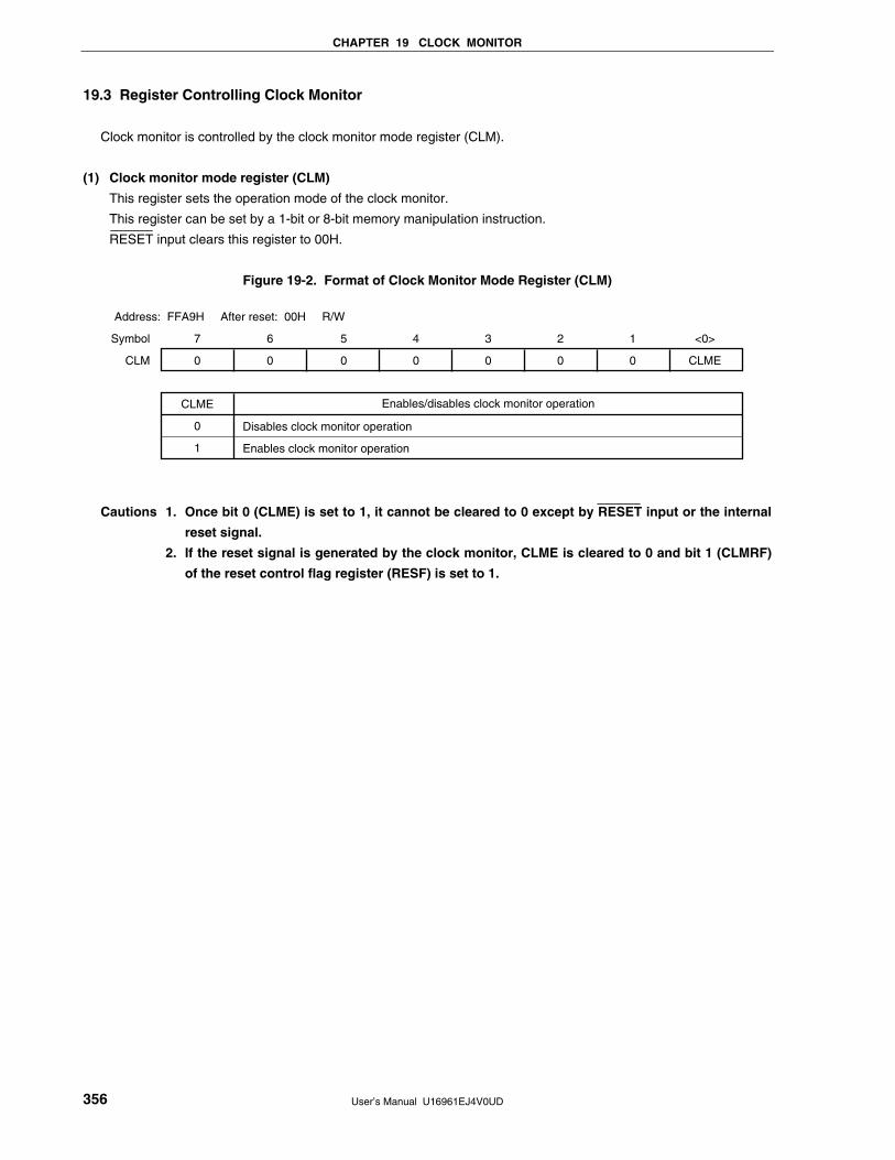
CHAPTER 19 CLOCK MONITOR
User’s Manual U16961EJ4V0UD 356
19.3 Register Controlling Clock Monitor
Clock monitor is controlled by the clock monitor mode register (CLM).
(1) Clock monitor mode register (CLM)
This register sets the operation mode of the clock monitor.
This register can be set by a 1-bit or 8-bit memory manipulation instruction.
RESET input clears this register to 00H.
Figure 19-2. Format of Clock Monitor Mode Register (CLM)
7
0
CLME
0
1
Symbol
CLM
Address: FFA9H After reset: 00H R/W
6
0
Disables clock monitor operation
Enables clock monitor operation
5
0
4
0
3
0
Enables/disables clock monitor operation
2
0
1
0
<0>
CLME
Cautions 1. Once bit 0 (CLME) is set to 1, it cannot be cleared to 0 except by RESET input or the internal
reset signal.
2. If the reset signal is generated by the clock monitor, CLME is cleared to 0 and bit 1 (CLMRF)
of the reset control flag register (RESF) is set to 1.
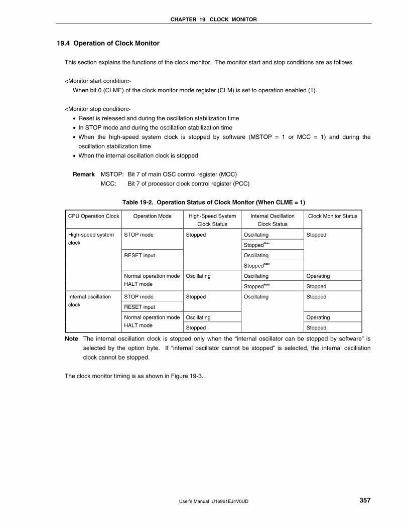
CHAPTER 19 CLOCK MONITOR
User’s Manual U16961EJ4V0UD 357
19.4 Operation of Clock Monitor
This section explains the functions of the clock monitor. The monitor start and stop conditions are as follows.
<Monitor start condition>
When bit 0 (CLME) of the clock monitor mode register (CLM) is set to operation enabled (1).
<Monitor stop condition>
• Reset is released and during the oscillation stabilization time
• In STOP mode and during the oscillation stabilization time
• When the high-speed system clock is stopped by software (MSTOP = 1 or MCC = 1) and during the
oscillation stabilization time
• When the internal oscillation clock is stopped
Remark MSTOP: Bit 7 of main OSC control register (MOC)
MCC: Bit 7 of processor clock control register (PCC)
Table 19-2. Operation Status of Clock Monitor (When CLME = 1)
CPU Operation Clock Operation Mode High-Speed System
Clock Status
Internal Oscillation
Clock Status
Clock Monitor Status
Oscillating STOP mode Stopped
StoppedNote
Oscillating RESET input
StoppedNote
Stopped
Oscillating Operating
High-speed system
clock
Normal operation mode
HALT mode
Oscillating
StoppedNote Stopped
STOP mode
RESET input
Stopped Oscillating Stopped
Oscillating Operating
Internal oscillation
clock
Normal operation mode
HALT mode Stopped Stopped
Note The internal oscillation clock is stopped only when the “internal oscillator can be stopped by software” is
selected by the option byte. If “internal oscillator cannot be stopped” is selected, the internal oscillation
clock cannot be stopped.
The clock monitor timing is as shown in Figure 19-3.
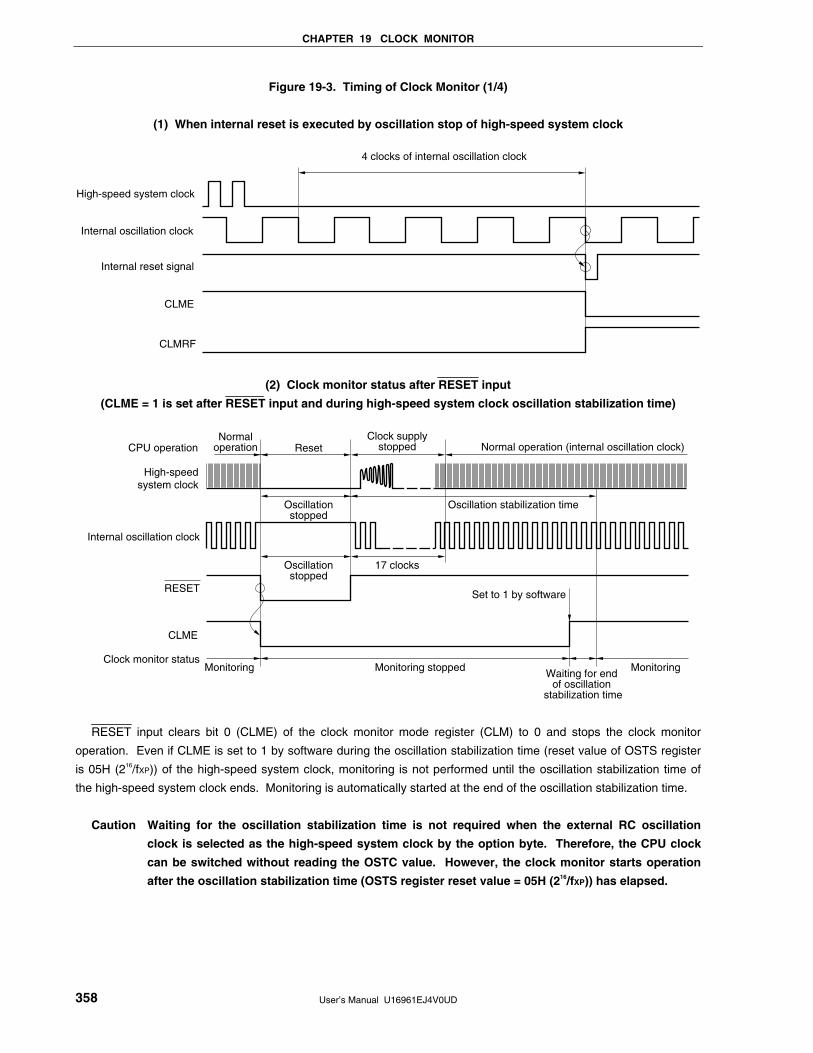
CHAPTER 19 CLOCK MONITOR
User’s Manual U16961EJ4V0UD 358
Figure 19-3. Timing of Clock Monitor (1/4)
(1) When internal reset is executed by oscillation stop of high-speed system clock
4 clocks of internal oscillation clock
High-speed system clock
Internal oscillation clock
Internal reset signal
CLME
CLMRF
(2) Clock monitor status after RESET input
(CLME = 1 is set after RESET input and during high-speed system clock oscillation stabilization time)
CPU operation
Clock monitor status
CLME
Internal oscillation clock
High-speedsystem clock
Reset
Oscillationstopped
Oscillation stabilization time
Normaloperation
Clock supplystopped Normal operation (internal oscillation clock)
Monitoring Monitoring stopped MonitoringWaiting for end
of oscillation stabilization time
Oscillationstopped
17 clocks
Set to 1 by softwareRESET
RESET input clears bit 0 (CLME) of the clock monitor mode register (CLM) to 0 and stops the clock monitor
operation. Even if CLME is set to 1 by software during the oscillation stabilization time (reset value of OSTS register
is 05H (216/fXP)) of the high-speed system clock, monitoring is not performed until the oscillation stabilization time of
the high-speed system clock ends. Monitoring is automatically started at the end of the oscillation stabilization time.
Caution Waiting for the oscillation stabilization time is not required when the external RC oscillation
clock is selected as the high-speed system clock by the option byte. Therefore, the CPU clock
can be switched without reading the OSTC value. However, the clock monitor starts operation
after the oscillation stabilization time (OSTS register reset value = 05H (216/fXP)) has elapsed.
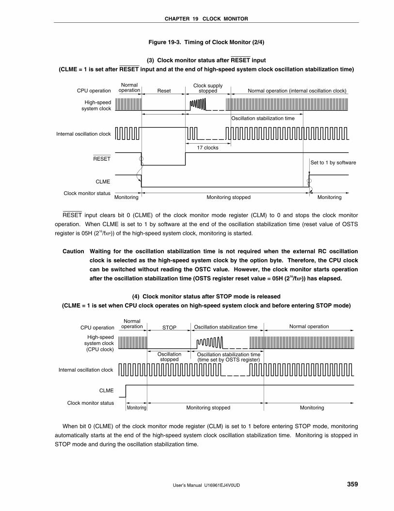
CHAPTER 19 CLOCK MONITOR
User’s Manual U16961EJ4V0UD 359
Figure 19-3. Timing of Clock Monitor (2/4)
(3) Clock monitor status after RESET input
(CLME = 1 is set after RESET input and at the end of high-speed system clock oscillation stabilization time)
CPU operation
Clock monitor status
CLME
RESET
Internal oscillation clock
High-speedsystem clock
Reset
Oscillation stabilization time
Normaloperation
Clock supplystopped Normal operation (internal oscillation clock)
Monitoring Monitoring stopped Monitoring
17 clocks
Set to 1 by software
RESET input clears bit 0 (CLME) of the clock monitor mode register (CLM) to 0 and stops the clock monitor
operation. When CLME is set to 1 by software at the end of the oscillation stabilization time (reset value of OSTS
register is 05H (216/fXP)) of the high-speed system clock, monitoring is started.
Caution Waiting for the oscillation stabilization time is not required when the external RC oscillation
clock is selected as the high-speed system clock by the option byte. Therefore, the CPU clock
can be switched without reading the OSTC value. However, the clock monitor starts operation
after the oscillation stabilization time (OSTS register reset value = 05H (216/fXP)) has elapsed.
(4) Clock monitor status after STOP mode is released
(CLME = 1 is set when CPU clock operates on high-speed system clock and before entering STOP mode)
Clock monitor statusMonitoring Monitoring stopped Monitoring
CLME
Internal oscillation clock
High-speedsystem clock(CPU clock)
CPU operationNormal
operation STOP Oscillation stabilization time Normal operation
Oscillationstopped
Oscillation stabilization time(time set by OSTS register)
When bit 0 (CLME) of the clock monitor mode register (CLM) is set to 1 before entering STOP mode, monitoring
automatically starts at the end of the high-speed system clock oscillation stabilization time. Monitoring is stopped in
STOP mode and during the oscillation stabilization time.
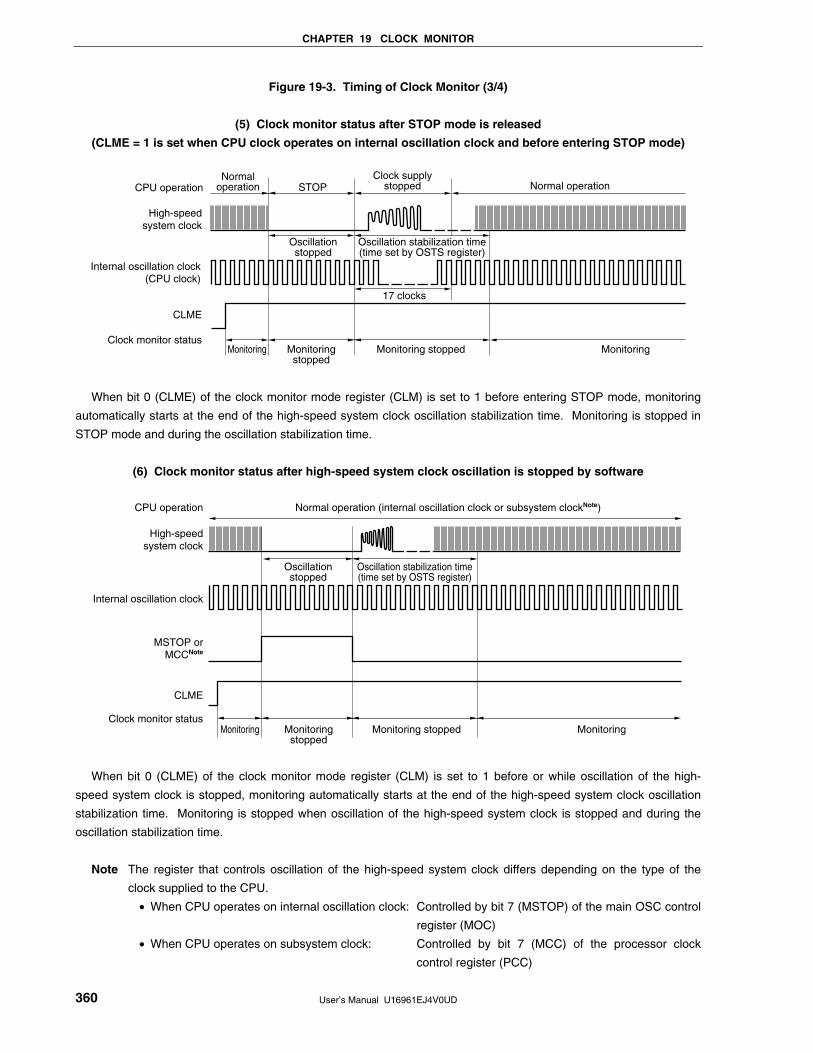
CHAPTER 19 CLOCK MONITOR
User’s Manual U16961EJ4V0UD 360
Figure 19-3. Timing of Clock Monitor (3/4)
(5) Clock monitor status after STOP mode is released
(CLME = 1 is set when CPU clock operates on internal oscillation clock and before entering STOP mode)
Clock monitor statusMonitoring Monitoring
stoppedMonitoring stopped Monitoring
CLME
Internal oscillation clock(CPU clock)
High-speedsystem clock
CPU operationNormal
operation
17 clocks
Clock supplystopped Normal operation
Oscillationstopped
Oscillation stabilization time(time set by OSTS register)
STOP
When bit 0 (CLME) of the clock monitor mode register (CLM) is set to 1 before entering STOP mode, monitoring
automatically starts at the end of the high-speed system clock oscillation stabilization time. Monitoring is stopped in
STOP mode and during the oscillation stabilization time.
(6) Clock monitor status after high-speed system clock oscillation is stopped by software
Clock monitor status
CLME
MSTOP orMCCNote
Internal oscillation clock
High-speedsystem clock
Oscillation stabilization time(time set by OSTS register)
Normal operation (internal oscillation clock or subsystem clockNote)
Monitoring Monitoringstopped
Monitoring
CPU operation
Monitoring stopped
Oscillationstopped
When bit 0 (CLME) of the clock monitor mode register (CLM) is set to 1 before or while oscillation of the high-
speed system clock is stopped, monitoring automatically starts at the end of the high-speed system clock oscillation
stabilization time. Monitoring is stopped when oscillation of the high-speed system clock is stopped and during the
oscillation stabilization time.
Note The register that controls oscillation of the high-speed system clock differs depending on the type of the
clock supplied to the CPU.
• When CPU operates on internal oscillation clock: Controlled by bit 7 (MSTOP) of the main OSC control
register (MOC)
• When CPU operates on subsystem clock: Controlled by bit 7 (MCC) of the processor clock
control register (PCC)
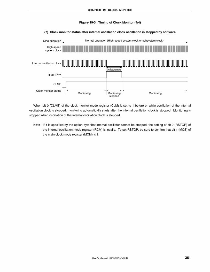
CHAPTER 19 CLOCK MONITOR
User’s Manual U16961EJ4V0UD 361
Figure 19-3. Timing of Clock Monitor (4/4)
(7) Clock monitor status after internal oscillation clock oscillation is stopped by software
Internal oscillation clock
High-speedsystem clock
CPU operation Normal operation (High-speed system clock or subsystem clock)
Oscillation stopped
RSTOPNote
Clock monitor statusMonitoring Monitoring
stoppedMonitoring
CLME
When bit 0 (CLME) of the clock monitor mode register (CLM) is set to 1 before or while oscillation of the internal
oscillation clock is stopped, monitoring automatically starts after the internal oscillation clock is stopped. Monitoring is
stopped when oscillation of the internal oscillation clock is stopped.
Note If it is specified by the option byte that internal oscillator cannot be stopped, the setting of bit 0 (RSTOP) of
the internal oscillation mode register (RCM) is invalid. To set RSTOP, be sure to confirm that bit 1 (MCS) of
the main clock mode register (MCM) is 1.
User’s Manual U16961EJ4V0UD 362
CHAPTER 20 POWER-ON-CLEAR CIRCUIT
20.1 Functions of Power-on-Clear Circuit
The power-on-clear circuit (POC) has the following functions.
• Generates internal reset signal at power on.
• Compares supply voltage (VDD) and detection voltage (VPOC = 2.1 V ±0.1 V), and generates internal reset signal
when VDD < VPOC.
Cautions 1. If an internal reset signal is generated in the POC circuit, the reset control flag register
(RESF) is cleared to 00H.
2. The supply voltage is VDD = 2.0 to 5.5 V when the Internal oscillation clock or subsystem
clock is used, but be sure to use the product in a voltage range of 2.2 to 5.5 V because the
detection voltage (VPOC) of the POC circuit is 2.1 V ±0.1 V.
3. The supply voltage is VDD = 2.0 to 5.5 V when the internal oscillation clock is used, but be
sure to use the (A1) grade products in a voltage range of 2.25 to 5.5 V because the detection
voltage (VPOC) of the POC circuit is 2.0 to 2.25 V.
Remark This product incorporates multiple hardware functions that generate an internal reset signal. A flag that
indicates the reset cause is located in the reset control flag register (RESF) for when an internal reset
signal is generated by the watchdog timer (WDT), low-voltage-detection (LVI) circuit, or clock monitor.
RESF is not cleared to 00H and the flag is set to 1 when an internal reset signal is generated by WDT,
LVI, or the clock monitor.
For details of the RESF, refer to CHAPTER 18 RESET FUNCTION.
<R>
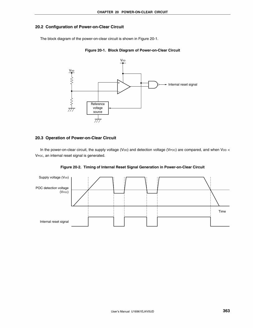
CHAPTER 20 POWER-ON-CLEAR CIRCUIT
User’s Manual U16961EJ4V0UD 363
20.2 Configuration of Power-on-Clear Circuit
The block diagram of the power-on-clear circuit is shown in Figure 20-1.
Figure 20-1. Block Diagram of Power-on-Clear Circuit
−
+
Referencevoltagesource
Internal reset signal
VDD
VDD
20.3 Operation of Power-on-Clear Circuit
In the power-on-clear circuit, the supply voltage (VDD) and detection voltage (VPOC) are compared, and when VDD <
VPOC, an internal reset signal is generated.
Figure 20-2. Timing of Internal Reset Signal Generation in Power-on-Clear Circuit
Time
Supply voltage (VDD)
POC detection voltage(VPOC)
Internal reset signal
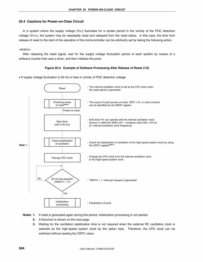
CHAPTER 20 POWER-ON-CLEAR CIRCUIT
User’s Manual U16961EJ4V0UD 364
20.4 Cautions for Power-on-Clear Circuit
In a system where the supply voltage (VDD) fluctuates for a certain period in the vicinity of the POC detection
voltage (VPOC), the system may be repeatedly reset and released from the reset status. In this case, the time from
release of reset to the start of the operation of the microcontroller can be arbitrarily set by taking the following action.
<Action>
After releasing the reset signal, wait for the supply voltage fluctuation period of each system by means of a
software counter that uses a timer, and then initialize the ports.
Figure 20-3. Example of Software Processing After Release of Reset (1/2)
• If supply voltage fluctuation is 50 ms or less in vicinity of POC detection voltage
Yes
Power-on-clear
; The internal oscillation clock is set as the CPU clock when the reset signal is generated
; The cause of reset (power-on-clear, WDT, LVI, or clock monitor) can be identified by the RESF register.
; Check the stabilization of oscillation of the high-speed system clock by using the OSTC registerNote 3.
; TMIFH1 = 1: Interrupt request is generated.
; Initialization of ports
No
Note 1
Reset
Checking causeof resetNote 2
Check stabilizationof oscillation
Change CPU clock
50 ms has passed?(TMIFH1 = 1?)
Initializationprocessing
Start timer(set to 50 ms)
; 8-bit timer H1 can operate with the internal oscillation clock.Source: fR (480 kHz (MAX.))/27 × compare value 200 = 53 ms(fR: internal oscillation clock frequency)
; Change the CPU clock from the internal oscillation clock to the high-speed system clock.
Notes 1. If reset is generated again during this period, initialization processing is not started.
2. A flowchart is shown on the next page.
3. Waiting for the oscillation stabilization time is not required when the external RC oscillation clock is
selected as the high-speed system clock by the option byte. Therefore, the CPU clock can be
switched without reading the OSTC value.
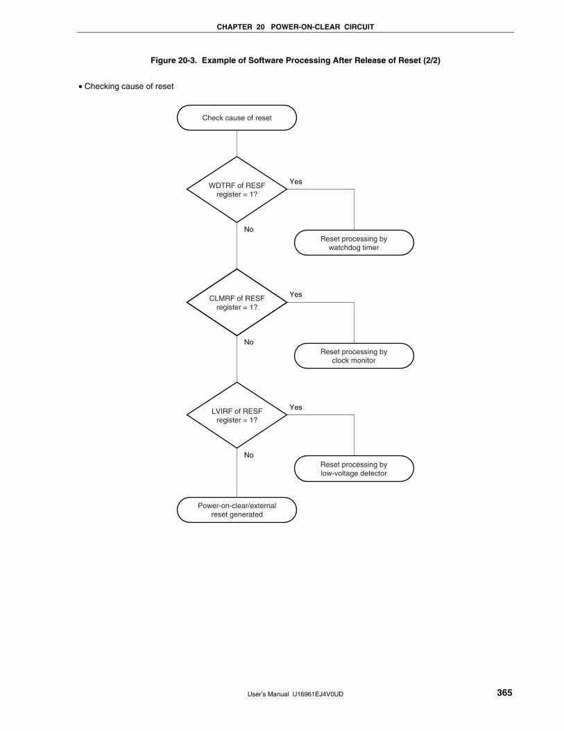
CHAPTER 20 POWER-ON-CLEAR CIRCUIT
User’s Manual U16961EJ4V0UD 365
Figure 20-3. Example of Software Processing After Release of Reset (2/2)
• Checking cause of reset
Yes
No
Check cause of reset
Power-on-clear/externalreset generated
Reset processing bywatchdog timer
Reset processing byclock monitor
Reset processing bylow-voltage detector
No
No
WDTRF of RESFregister = 1?
CLMRF of RESFregister = 1?
LVIRF of RESFregister = 1?
Yes
Yes
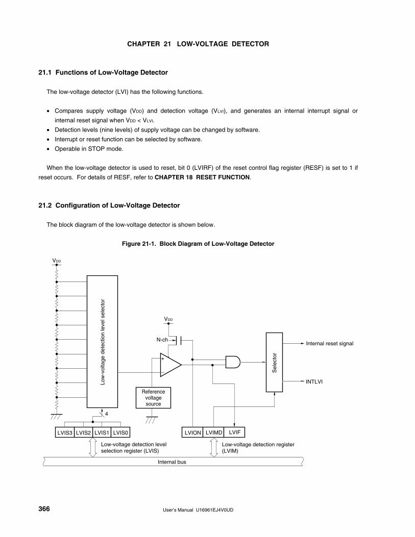
User’s Manual U16961EJ4V0UD 366
CHAPTER 21 LOW-VOLTAGE DETECTOR
21.1 Functions of Low-Voltage Detector
The low-voltage detector (LVI) has the following functions.
• Compares supply voltage (VDD) and detection voltage (VLVI), and generates an internal interrupt signal or
internal reset signal when VDD < VLVI.
• Detection levels (nine levels) of supply voltage can be changed by software.
• Interrupt or reset function can be selected by software.
• Operable in STOP mode.
When the low-voltage detector is used to reset, bit 0 (LVIRF) of the reset control flag register (RESF) is set to 1 if
reset occurs. For details of RESF, refer to CHAPTER 18 RESET FUNCTION.
21.2 Configuration of Low-Voltage Detector
The block diagram of the low-voltage detector is shown below.
Figure 21-1. Block Diagram of Low-Voltage Detector
LVIS1 LVIS0 LVION
−
+
Referencevoltagesource
VDD
Internal bus
N-ch
Low-voltage detection level selection register (LVIS)
Low-voltage detection register(LVIM)
LVIS2LVIS3 LVIMD LVIF
INTLVI
Internal reset signal
4
VDD
Low
-vol
tage
det
ectio
n le
vel s
elec
tor
Sel
ecto
r
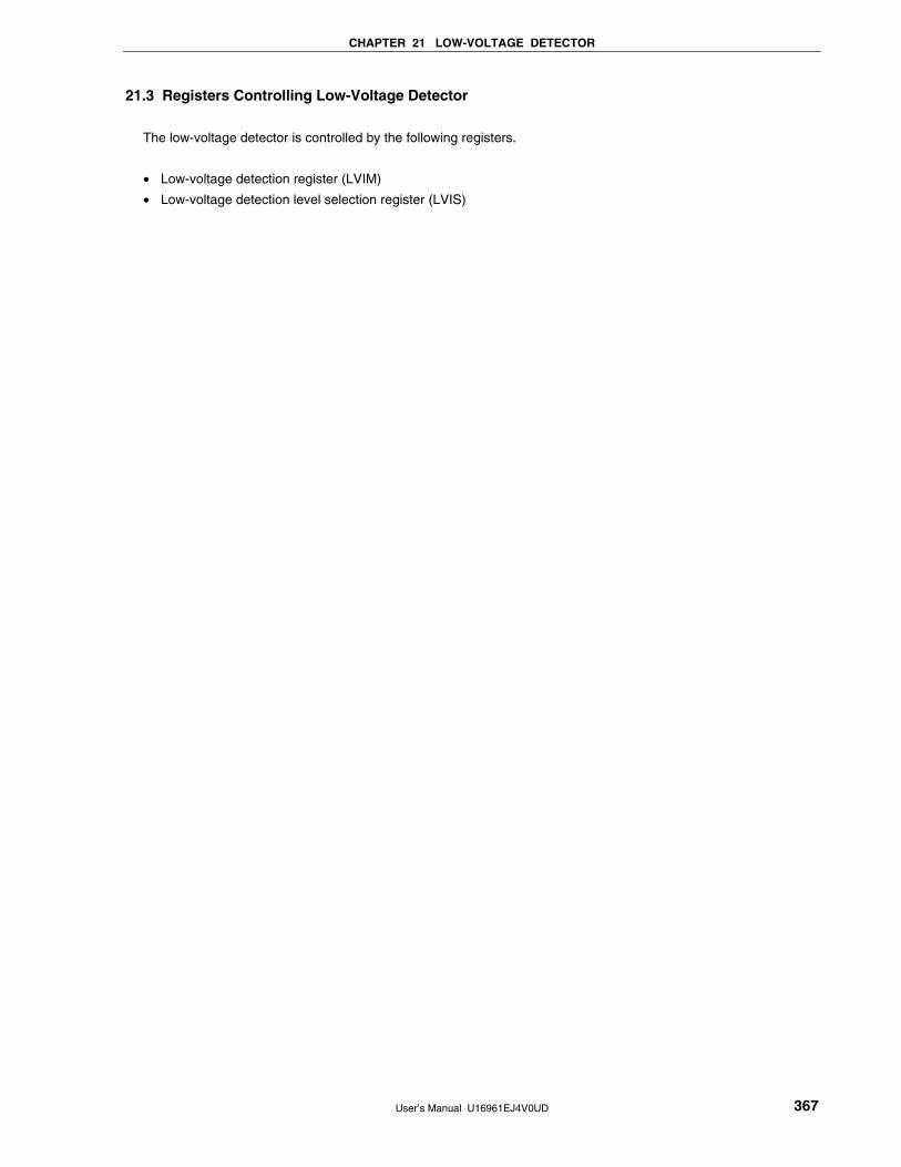
CHAPTER 21 LOW-VOLTAGE DETECTOR
User’s Manual U16961EJ4V0UD 367
21.3 Registers Controlling Low-Voltage Detector
The low-voltage detector is controlled by the following registers.
• Low-voltage detection register (LVIM)
• Low-voltage detection level selection register (LVIS)
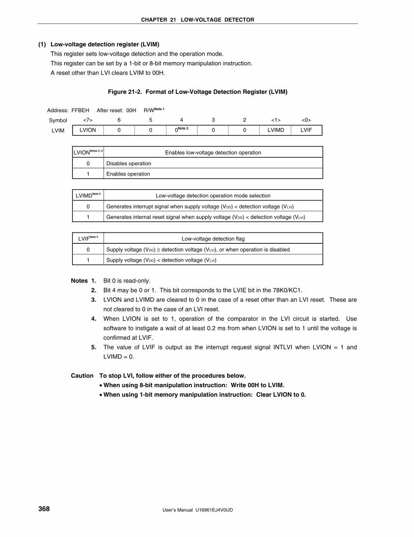
CHAPTER 21 LOW-VOLTAGE DETECTOR
User’s Manual U16961EJ4V0UD 368
(1) Low-voltage detection register (LVIM)
This register sets low-voltage detection and the operation mode.
This register can be set by a 1-bit or 8-bit memory manipulation instruction.
A reset other than LVI clears LVIM to 00H.
Figure 21-2. Format of Low-Voltage Detection Register (LVIM)
<0>
LVIF
<1>
LVIMD
2
0
3
0
4
0Note 2
5
0
6
0
<7>
LVION
Symbol
LVIM
Address: FFBEH After reset: 00H R/WNote 1
LVIONNotes 3, 4 Enables low-voltage detection operation
0 Disables operation
1 Enables operation
LVIMDNote 3 Low-voltage detection operation mode selection
0 Generates interrupt signal when supply voltage (VDD) < detection voltage (VLVI)
1 Generates internal reset signal when supply voltage (VDD) < detection voltage (VLVI)
LVIFNote 5 Low-voltage detection flag
0 Supply voltage (VDD) ≥ detection voltage (VLVI), or when operation is disabled
1 Supply voltage (VDD) < detection voltage (VLVI)
Notes 1. Bit 0 is read-only.
2. Bit 4 may be 0 or 1. This bit corresponds to the LVIE bit in the 78K0/KC1.
3. LVION and LVIMD are cleared to 0 in the case of a reset other than an LVI reset. These are
not cleared to 0 in the case of an LVI reset.
4. When LVION is set to 1, operation of the comparator in the LVI circuit is started. Use
software to instigate a wait of at least 0.2 ms from when LVION is set to 1 until the voltage is
confirmed at LVIF.
5. The value of LVIF is output as the interrupt request signal INTLVI when LVION = 1 and
LVIMD = 0.
Caution To stop LVI, follow either of the procedures below.
• When using 8-bit manipulation instruction: Write 00H to LVIM.
• When using 1-bit memory manipulation instruction: Clear LVION to 0.
CHAPTER 21 LOW-VOLTAGE DETECTOR
User’s Manual U16961EJ4V0UD 369
(2) Low-voltage detection level selection register (LVIS)
This register selects the low-voltage detection level.
This register can be set by an 8-bit memory manipulation instruction.
A reset other than LVI clears LVIM to 00H.
Figure 21-3. Format of Low-Voltage Detection Level Selection Register (LVIS)
0
LVIS0
1
LVIS1
2
LVIS2
3
LVIS3
4
0
5
0
6
0
7
0
Symbol
LVIS
Address: FFBFH After reset: 00H R/W
LVIS3 LVIS2 LVIS1 LVIS0 Detection level
0 0 0 0 VLVI0 (4.3 V ±0.2 V)
0 0 0 1 VLVI1 (4.1 V ±0.2 V)
0 0 1 0 VLVI2 (3.9 V ±0.2 V)
0 0 1 1 VLVI3 (3.7 V ±0.2 V)
0 1 0 0 VLVI4 (3.5 V ±0.2 V)
0 1 0 1 VLVI5 (3.3 V ±0.15 V)
0 1 1 0 VLVI6 (3.1 V ±0.15 V)
0 1 1 1 VLVI7 (2.85 V ±0.15 V)
1 0 0 0 VLVI8 (2.6 V ±0.1 V)Note
1 0 0 1 VLVI9 (2.35 V ±0.1 V)Note
Other than above Setting prohibited
Note Do not set VLVI8 or VLVI9 when using the standard products and (A) grade products to evaluate the
program of a mask ROM version of the 78K0/KC1 or when using the (A1) grade products.
Cautions 1. Be sure to clear bits 4 to 7 to 0.
2. Clear all port pins after the supply voltage (VDD) exceeds the preset detection
voltage (VLVI) after POC release in the (A1) grade products.
<R>
<R>
CHAPTER 21 LOW-VOLTAGE DETECTOR
User’s Manual U16961EJ4V0UD 370
21.4 Operation of Low-Voltage Detector
The low-voltage detector can be used in the following two modes.
• Used as reset
Compares the supply voltage (VDD) and detection voltage (VLVI), and generates an internal reset signal when
VDD < VLVI.
• Used as interrupt
Compares the supply voltage (VDD) and detection voltage (VLVI), and generates an interrupt signal (INTLVI)
when VDD < VLVI.
The operation is set as follows.
(1) When used as reset
• When starting operation
<1> Mask the LVI interrupt (LVIMK = 1).
<2> Set the detection voltage using bits 3 to 0 (LVIS3 to LVIS0) of the low-voltage detection level selection
register (LVIS).
<3> Set bit 7 (LVION) of LVIM to 1 (enables LVI operation).
<4> Use software to instigate a wait of at least 0.2 ms.
<5> Confirm that “supply voltage (VDD) ≥ detection voltage (VLVI)” with bit 0 (LVIF) of LVIM.
<6> Set bit 1 (LVIMD) of LVIM to 1 (generates internal reset signal when supply voltage (VDD) < detection
voltage (VLVI)).
Figure 21-4 shows the timing of the internal reset signal generated by the low-voltage detector. The numbers
in this timing chart correspond to <1> to <6> above.
Cautions 1. <1> must always be executed. When LVIMK = 0, an interrupt may occur immediately
after the processing in <3>.
2. If supply voltage (VDD) ≥ detection voltage (VLVI) when LVIMD is set to 1, an internal reset
signal is not generated.
• When stopping operation
Either of the following procedures must be executed.
• When using 8-bit memory manipulation instruction:
Write 00H to LVIM.
• When using 1-bit memory manipulation instruction:
Clear LVIMD to 0 first, and then clear LVION to 0.
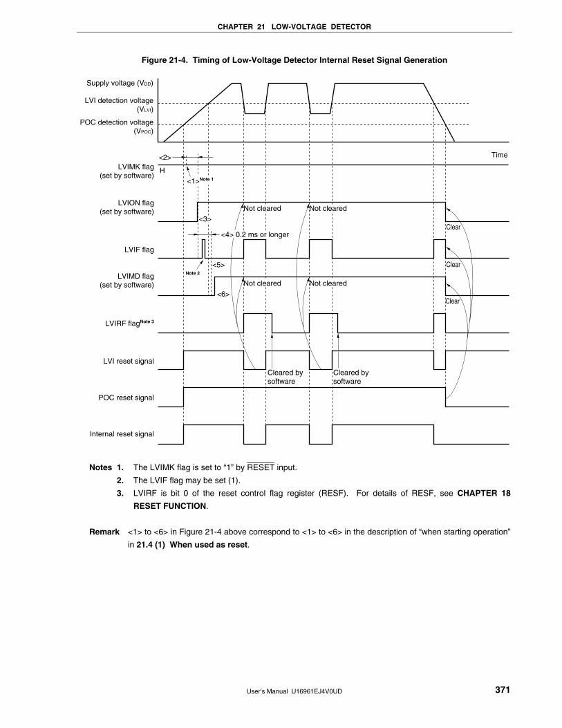
CHAPTER 21 LOW-VOLTAGE DETECTOR
User’s Manual U16961EJ4V0UD 371
Figure 21-4. Timing of Low-Voltage Detector Internal Reset Signal Generation
Supply voltage (VDD)
LVI detection voltage(VLVI)
POC detection voltage(VPOC)
<2> Time
LVIMK flag(set by software)
LVIF flag
LVIRF flagNote 3
Note 2
LVI reset signal
POC reset signal
Internal reset signal
Cleared bysoftware
Not cleared Not cleared
Not cleared Not cleared
Cleared bysoftware
<5>
<6>
Clear
Clear
Clear
<4> 0.2 ms or longer
LVION flag(set by software)
LVIMD flag(set by software)
H<1>Note 1
<3>
Notes 1. The LVIMK flag is set to “1” by RESET input.
2. The LVIF flag may be set (1).
3. LVIRF is bit 0 of the reset control flag register (RESF). For details of RESF, see CHAPTER 18
RESET FUNCTION.
Remark <1> to <6> in Figure 21-4 above correspond to <1> to <6> in the description of “when starting operation”
in 21.4 (1) When used as reset.
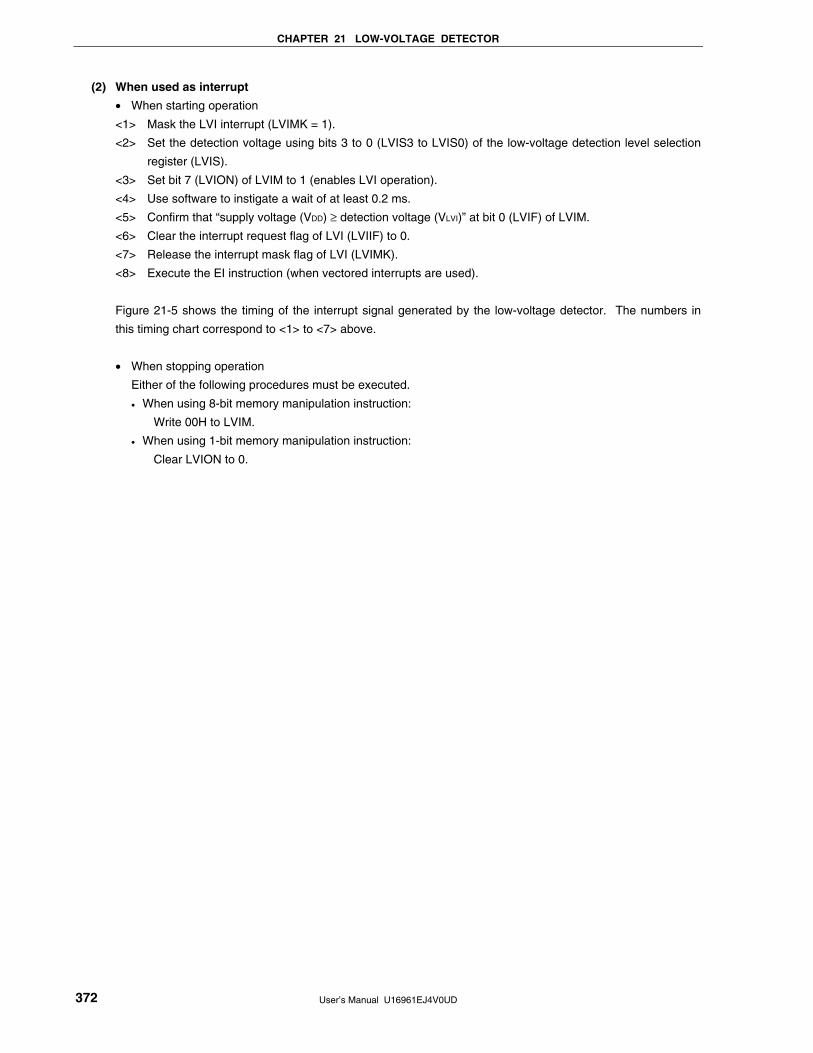
CHAPTER 21 LOW-VOLTAGE DETECTOR
User’s Manual U16961EJ4V0UD 372
(2) When used as interrupt
• When starting operation
<1> Mask the LVI interrupt (LVIMK = 1).
<2> Set the detection voltage using bits 3 to 0 (LVIS3 to LVIS0) of the low-voltage detection level selection
register (LVIS).
<3> Set bit 7 (LVION) of LVIM to 1 (enables LVI operation).
<4> Use software to instigate a wait of at least 0.2 ms.
<5> Confirm that “supply voltage (VDD) ≥ detection voltage (VLVI)” at bit 0 (LVIF) of LVIM.
<6> Clear the interrupt request flag of LVI (LVIIF) to 0.
<7> Release the interrupt mask flag of LVI (LVIMK).
<8> Execute the EI instruction (when vectored interrupts are used).
Figure 21-5 shows the timing of the interrupt signal generated by the low-voltage detector. The numbers in
this timing chart correspond to <1> to <7> above.
• When stopping operation
Either of the following procedures must be executed.
• When using 8-bit memory manipulation instruction:
Write 00H to LVIM.
• When using 1-bit memory manipulation instruction:
Clear LVION to 0.
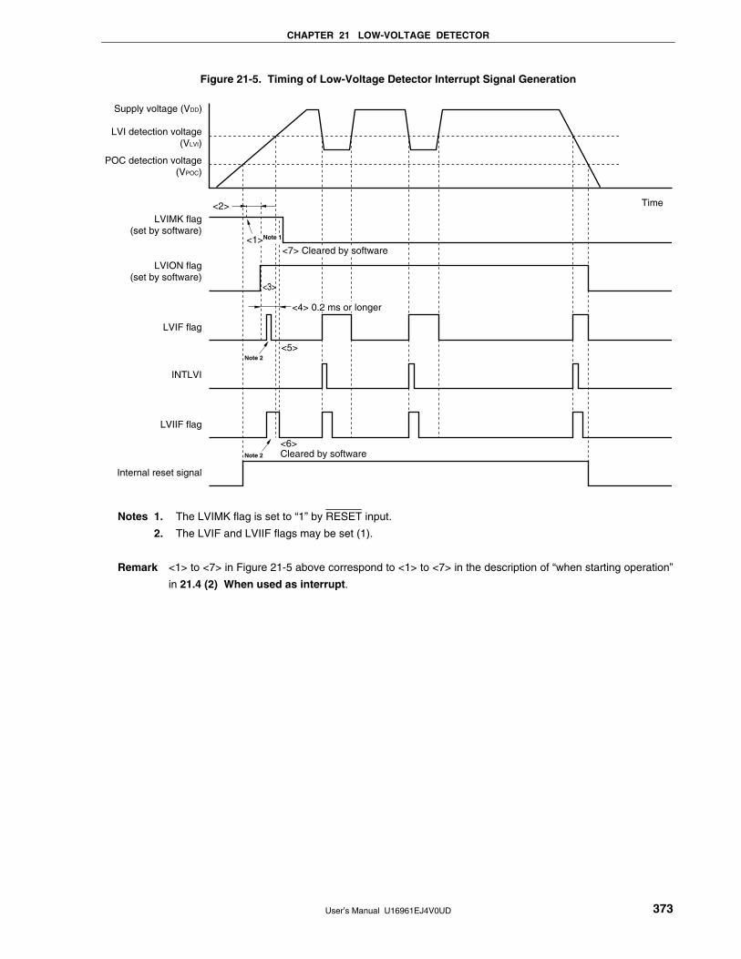
CHAPTER 21 LOW-VOLTAGE DETECTOR
User’s Manual U16961EJ4V0UD 373
Figure 21-5. Timing of Low-Voltage Detector Interrupt Signal Generation
Supply voltage (VDD)
LVI detection voltage(VLVI)
POC detection voltage(VPOC)
Time<2>
<7> Cleared by software
LVIMK flag(set by software)
LVIF flag
INTLVI
LVIIF flag
Internal reset signal
<3>
<5>
<6>Cleared by software
<4> 0.2 ms or longer
LVION flag(set by software)
Note 2
Note 2
<1>Note 1
Notes 1. The LVIMK flag is set to “1” by RESET input.
2. The LVIF and LVIIF flags may be set (1).
Remark <1> to <7> in Figure 21-5 above correspond to <1> to <7> in the description of “when starting operation”
in 21.4 (2) When used as interrupt.
CHAPTER 21 LOW-VOLTAGE DETECTOR
User’s Manual U16961EJ4V0UD 374
21.5 Cautions for Low-Voltage Detector
In a system where the supply voltage (VDD) fluctuates for a certain period in the vicinity of the LVI detection voltage
(VLVI), the operation is as follows depending on how the low-voltage detector is used.
(1) When used as reset
The system may be repeatedly reset and released from the reset status.
In this case, the time from release of reset to the start of the operation of the microcontroller can be arbitrarily set
by taking action (a) below.
(2) When used as interrupt
Interrupt requests may be frequently generated. Take action (b) below.
In this system, take the following actions.
<Action>
(a) When used as reset
After releasing the reset signal, wait for the supply voltage fluctuation period of each system by means of a
software counter that uses a timer, and then initialize the ports.
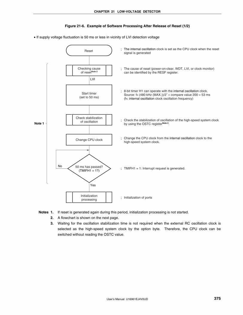
CHAPTER 21 LOW-VOLTAGE DETECTOR
User’s Manual U16961EJ4V0UD 375
Figure 21-6. Example of Software Processing After Release of Reset (1/2)
• If supply voltage fluctuation is 50 ms or less in vicinity of LVI detection voltage
Yes
LVI
; The internal oscillation clock is set as the CPU clock when the reset signal is generated
; The cause of reset (power-on-clear, WDT, LVI, or clock monitor) can be identified by the RESF register.
; Change the CPU clock from the internal oscillation clock to the high-speed system clock.
; Check the stabilization of oscillation of the high-speed system clock by using the OSTC registerNote 3.
; TMIFH1 = 1: Interrupt request is generated.
; Initialization of ports
; 8-bit timer H1 can operate with the internal oscillation clock.Source: fR (480 kHz (MAX.))/27 × compare value 200 = 53 ms(fR: internal oscillation clock oscillation frequency)
No
Note 1
Reset
Checking causeof resetNote 2
Check stabilizationof oscillation
Change CPU clock
50 ms has passed?(TMIFH1 = 1?)
Initializationprocessing
Start timer(set to 50 ms)
Notes 1. If reset is generated again during this period, initialization processing is not started.
2. A flowchart is shown on the next page.
3. Waiting for the oscillation stabilization time is not required when the external RC oscillation clock is
selected as the high-speed system clock by the option byte. Therefore, the CPU clock can be
switched without reading the OSTC value.
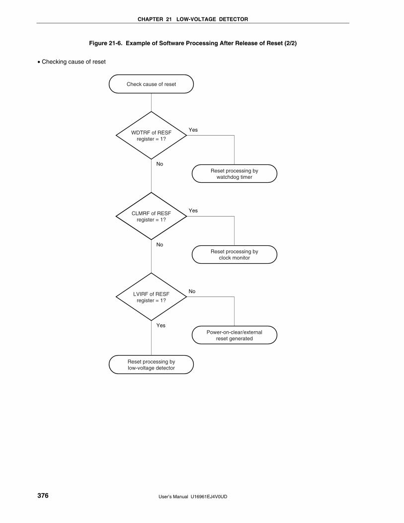
CHAPTER 21 LOW-VOLTAGE DETECTOR
User’s Manual U16961EJ4V0UD 376
Figure 21-6. Example of Software Processing After Release of Reset (2/2)
• Checking cause of reset
Yes
No
Check cause of reset
Power-on-clear/externalreset generated
Reset processing bywatchdog timer
Reset processing byclock monitor
Reset processing bylow-voltage detector
No
Yes
WDTRF of RESFregister = 1?
CLMRF of RESFregister = 1?
LVIRF of RESFregister = 1?
Yes
No
CHAPTER 21 LOW-VOLTAGE DETECTOR
User’s Manual U16961EJ4V0UD 377
(b) When used as interrupt
Check that “supply voltage (VDD) ≥ detection voltage (VLVI)” in the servicing routine of the LVI interrupt by
using bit 0 (LVIF) of the low-voltage detection register (LVIM). Clear bit 0 (LVIIF) of interrupt request flag
register 0L (IF0L) to 0 and enable interrupts (EI).
In a system where the supply voltage fluctuation period is long in the vicinity of the LVI detection voltage, wait
for the supply voltage fluctuation period, check that “supply voltage (VDD) ≥ detection voltage (VLVI)” using the
LVIF flag, and then enable interrupts (EI).
User’s Manual U16961EJ4V0UD 378
CHAPTER 22 OPTION BYTE
22.1 Functions of Option Bytes
The flash memory at 0080H to 0084H of the 78K0/KC1+ is an option byte area. When power is turned on or when
the device is restarted from the reset status, the device automatically references the option bytes and sets specified
functions. When using the product, be sure to set the following functions by using the option bytes.
When the boot swap operation is used during self-programming, 0080H to 0084H are switched to 1080H to 1084H.
Therefore, set values that are the same as those of 0080H to 0084H to 1080H to 1084H in advance.
(1) 0080H/1080H
Selection of high-speed system clock oscillation
• Crystal/ceramic oscillator
• External RC oscillator
Internal oscillator operation
• Can be stopped by software
• Cannot be stopped
(2) 0084H/1084H
On-chip debug operation control
• Disabling on-chip debug operation
• Enabling on-chip debug operation and erasing data of the flash memory in case authentication of the on-
chip debug security ID fails
• Enabling on-chip debug operation and not erasing data of the flash memory even in case authentication of
the on-chip debug security ID fails
Cautions 1. Be sure to set 00H (disabling on-chip debug operation) to 0084H for products not equipped with the on-chip debug function (µPD78F0112H, 78F0113H, 78F0114H). Also set 00H to 1084H because 0084H and 1084H are switched at boot swapping.
2. To use the on-chip debug function with a product equipped with the on-chip debug function (µPD78F0114HD), set 02H or 03H to 0084H. Set a value that is the same as that of 0084H to 1084H because 0084H and 1084H are switched at boot swapping.
Caution Be sure to set 00H to 0081H, 0082H, and 0083H (0081H/1081H, 0082H/1082H, and 0083H/1083H
when the boot swap function is used).
22.2 Format of Option Byte
The format of the option byte is shown below.
<R>
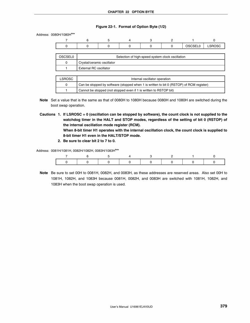
CHAPTER 22 OPTION BYTE
User’s Manual U16961EJ4V0UD 379
Figure 22-1. Format of Option Byte (1/2)
Address: 0080H/1080HNote
7 6 5 4 3 2 1 0
0 0 0 0 0 0 OSCSEL0 LSROSC
OSCSEL0 Selection of high-speed system clock oscillation
0 Crystal/ceramic oscillator
1 External RC oscillator
LSROSC Internal oscillator operation
0 Can be stopped by software (stopped when 1 is written to bit 0 (RSTOP) of RCM register)
1 Cannot be stopped (not stopped even if 1 is written to RSTOP bit)
Note Set a value that is the same as that of 0080H to 1080H because 0080H and 1080H are switched during the
boot swap operation.
Cautions 1. If LSROSC = 0 (oscillation can be stopped by software), the count clock is not supplied to the watchdog timer in the HALT and STOP modes, regardless of the setting of bit 0 (RSTOP) of the internal oscillation mode register (RCM).
When 8-bit timer H1 operates with the internal oscillation clock, the count clock is supplied to 8-bit timer H1 even in the HALT/STOP mode.
2. Be sure to clear bit 2 to 7 to 0.
Address: 0081H/1081H, 0082H/1082H, 0083H/1083HNote
7 6 5 4 3 2 1 0
0 0 0 0 0 0 0 0
Note Be sure to set 00H to 0081H, 0082H, and 0083H, as these addresses are reserved areas. Also set 00H to
1081H, 1082H, and 1083H because 0081H, 0082H, and 0083H are switched with 1081H, 1082H, and
1083H when the boot swap operation is used.
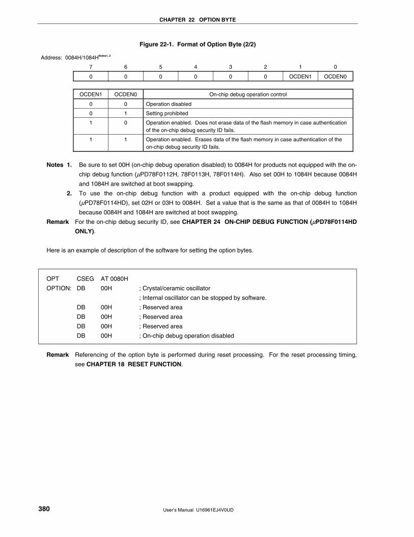
CHAPTER 22 OPTION BYTE
User’s Manual U16961EJ4V0UD 380
Figure 22-1. Format of Option Byte (2/2)
Address: 0084H/1084HNotes1, 2
7 6 5 4 3 2 1 0
0 0 0 0 0 0 OCDEN1 OCDEN0
OCDEN1 OCDEN0 On-chip debug operation control
0 0 Operation disabled
0 1 Setting prohibited
1 0 Operation enabled. Does not erase data of the flash memory in case authentication of the on-chip debug security ID fails.
1 1 Operation enabled. Erases data of the flash memory in case authentication of the on-chip debug security ID fails.
Notes 1. Be sure to set 00H (on-chip debug operation disabled) to 0084H for products not equipped with the on-
chip debug function (µPD78F0112H, 78F0113H, 78F0114H). Also set 00H to 1084H because 0084H
and 1084H are switched at boot swapping.
2. To use the on-chip debug function with a product equipped with the on-chip debug function
(µPD78F0114HD), set 02H or 03H to 0084H. Set a value that is the same as that of 0084H to 1084H
because 0084H and 1084H are switched at boot swapping.
Remark For the on-chip debug security ID, see CHAPTER 24 ON-CHIP DEBUG FUNCTION (µPD78F0114HD
ONLY).
Here is an example of description of the software for setting the option bytes.
OPT CSEG AT 0080H
OPTION: DB 00H ; Crystal/ceramic oscillator
; Internal oscillator can be stopped by software.
DB 00H ; Reserved area
DB 00H ; Reserved area
DB 00H ; Reserved area
DB 00H ; On-chip debug operation disabled
Remark Referencing of the option byte is performed during reset processing. For the reset processing timing,
see CHAPTER 18 RESET FUNCTION.
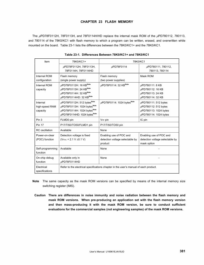
User’s Manual U16961EJ4V0UD 381
CHAPTER 23 FLASH MEMORY
The μPD78F0112H, 78F0113H, and 78F0114H/HD replace the internal mask ROM of the μPD780112, 780113, and 780114 of the 78K0/KC1 with flash memory to which a program can be written, erased, and overwritten while mounted on the board. Table 23-1 lists the differences between the 78K0/KC1+ and the 78K0/KC1.
Table 23-1. Differences Between 78K0/KC1+ and 78K0/KC1
78K0/KC1+ 78K0/KC1 Item
μPD78F0112H, 78F0113H, 78F0114H, 78F0114HD
μPD78F0114 μPD780111, 780112, 780113, 780114
Internal ROM configuration
Flash memory (single power supply)
Flash memory (two power supplies)
Mask ROM
Internal ROM capacity
μPD78F0112H: 16 KBNote μPD78F0113H: 24 KBNote μPD78F0114H: 32 KBNote μPD78F0114HD: 32 KBNote
μPD78F0114: 32 KBNote μPD780111: 8 KB μPD780112: 16 KB μPD780113: 24 KB μPD780114: 32 KB
Internal high-speed RAM capacity
μPD78F0112H: 512 bytesNote μPD78F0113H: 1024 bytesNote
μPD78F0114H: 1024 bytesNote
μPD78F0114HD: 1024 bytesNote
μPD78F0114: 1024 bytesNote μPD780111: 512 bytes μPD780112: 512 bytes μPD780113: 1024 bytes μPD780114: 1024 bytes
Pin 3 FLMD0 pin VPP pin IC pin
Pin 17 P17/TI50/TO50/FLMD1 pin P17/TI50/TO50 pin
RC oscillation Available None
Power-on-clear (POC) function
Detection voltage is fixed (VPOC = 2.1 V ±0.1 V)
Enabling use of POC and detection voltage selectable by product
Enabling use of POC and detection voltage selectable by mask option
Self-programming function
Available None −
On-chip debug function
Available only in μPD78F0114HD
None −
Electrical specifications
Refer to the electrical specifications chapter in the user’s manual of each product.
Note The same capacity as the mask ROM versions can be specified by means of the internal memory size
switching register (IMS).
Caution There are differences in noise immunity and noise radiation between the flash memory and mask ROM versions. When pre-producing an application set with the flash memory version and then mass-producing it with the mask ROM version, be sure to conduct sufficient evaluations for the commercial samples (not engineering samples) of the mask ROM versions.
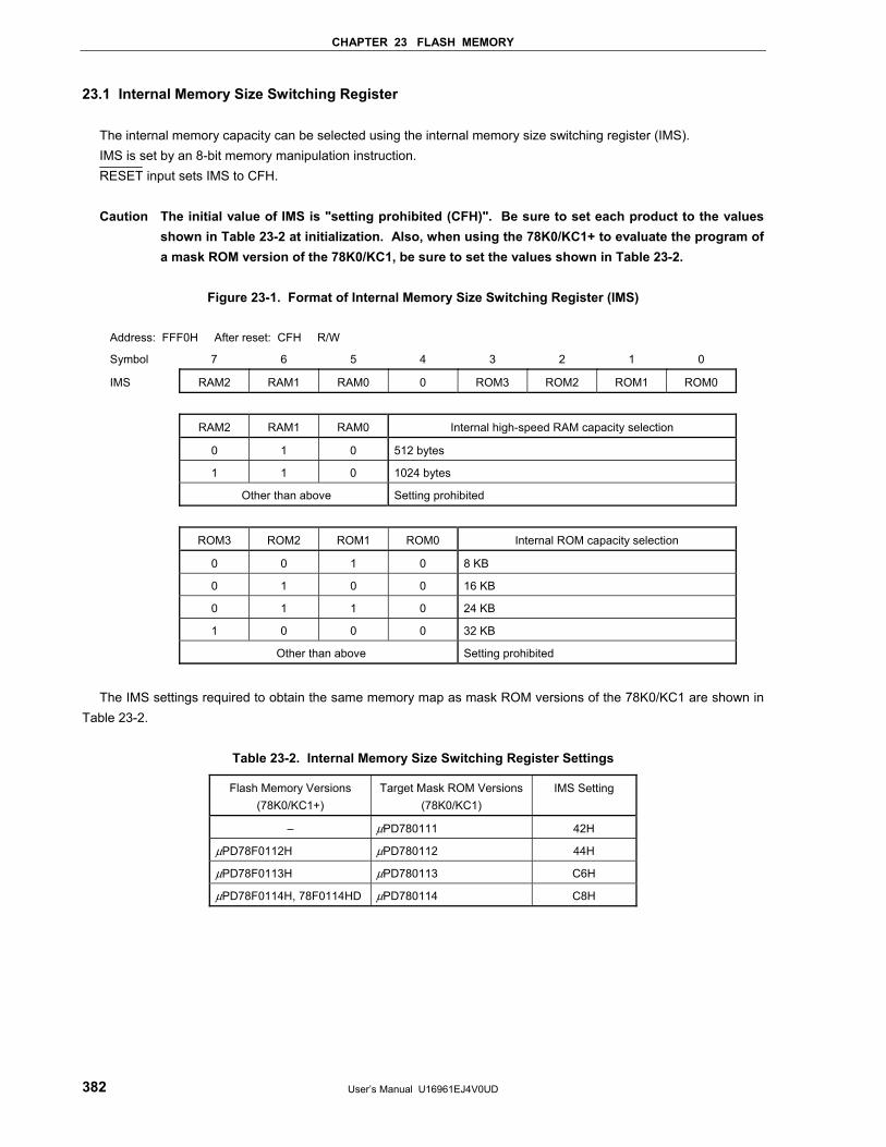
CHAPTER 23 FLASH MEMORY
User’s Manual U16961EJ4V0UD 382
23.1 Internal Memory Size Switching Register
The internal memory capacity can be selected using the internal memory size switching register (IMS). IMS is set by an 8-bit memory manipulation instruction. RESET input sets IMS to CFH.
Caution The initial value of IMS is "setting prohibited (CFH)". Be sure to set each product to the values
shown in Table 23-2 at initialization. Also, when using the 78K0/KC1+ to evaluate the program of a mask ROM version of the 78K0/KC1, be sure to set the values shown in Table 23-2.
Figure 23-1. Format of Internal Memory Size Switching Register (IMS)
Address: FFF0H After reset: CFH R/W
Symbol 7 6 5 4 3 2 1 0
IMS RAM2 RAM1 RAM0 0 ROM3 ROM2 ROM1 ROM0
RAM2 RAM1 RAM0 Internal high-speed RAM capacity selection
0 1 0 512 bytes
1 1 0 1024 bytes
Other than above Setting prohibited
ROM3 ROM2 ROM1 ROM0 Internal ROM capacity selection
0 0 1 0 8 KB
0 1 0 0 16 KB
0 1 1 0 24 KB
1 0 0 0 32 KB
Other than above Setting prohibited
The IMS settings required to obtain the same memory map as mask ROM versions of the 78K0/KC1 are shown in
Table 23-2.
Table 23-2. Internal Memory Size Switching Register Settings
Flash Memory Versions (78K0/KC1+)
Target Mask ROM Versions (78K0/KC1)
IMS Setting
– μPD780111 42H
μPD78F0112H μPD780112 44H
μPD78F0113H μPD780113 C6H
μPD78F0114H, 78F0114HD μPD780114 C8H
CHAPTER 23 FLASH MEMORY
User’s Manual U16961EJ4V0UD 383
23.2 Writing with Flash Programmer
Data can be written to the flash memory on-board or off-board, by using a dedicated flash programmer. (1) On-board programming
The contents of the flash memory can be rewritten after the 78K0/KC1+ has been mounted on the target system. The connectors that connect the dedicated flash programmer must be mounted on the target system.
(2) Off-board programming
Data can be written to the flash memory with a dedicated program adapter (FA series) before the 78K0/KC1+ is mounted on the target system.
Remark The FA series is a product of Naito Densei Machida Mfg. Co., Ltd.
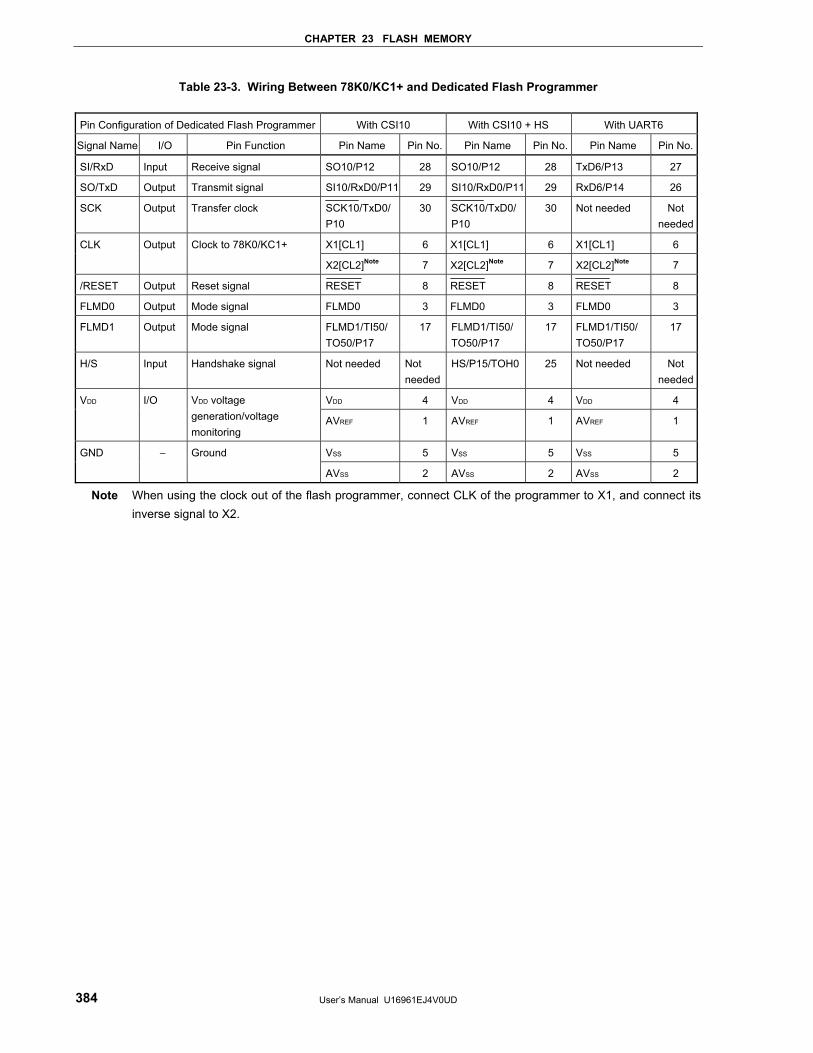
CHAPTER 23 FLASH MEMORY
User’s Manual U16961EJ4V0UD 384
Table 23-3. Wiring Between 78K0/KC1+ and Dedicated Flash Programmer Pin Configuration of Dedicated Flash Programmer With CSI10 With CSI10 + HS With UART6
Signal Name I/O Pin Function Pin Name Pin No. Pin Name Pin No. Pin Name Pin No.
SI/RxD Input Receive signal SO10/P12 28 SO10/P12 28 TxD6/P13 27
SO/TxD Output Transmit signal SI10/RxD0/P11 29 SI10/RxD0/P11 29 RxD6/P14 26
SCK Output Transfer clock SCK10/TxD0/P10
30 SCK10/TxD0/P10
30 Not needed Not needed
X1[CL1] 6 X1[CL1] 6 X1[CL1] 6 CLK Output Clock to 78K0/KC1+
X2[CL2]Note 7 X2[CL2]Note 7 X2[CL2]Note 7
/RESET Output Reset signal RESET 8 RESET 8 RESET 8
FLMD0 Output Mode signal FLMD0 3 FLMD0 3 FLMD0 3
FLMD1 Output Mode signal FLMD1/TI50/TO50/P17
17 FLMD1/TI50/TO50/P17
17 FLMD1/TI50/ TO50/P17
17
H/S Input Handshake signal Not needed Not needed
HS/P15/TOH0 25 Not needed Not needed
VDD 4 VDD 4 VDD 4 VDD I/O VDD voltage generation/voltage monitoring
AVREF 1 AVREF 1 AVREF 1
VSS 5 VSS 5 VSS 5 GND − Ground
AVSS 2 AVSS 2 AVSS 2
Note When using the clock out of the flash programmer, connect CLK of the programmer to X1, and connect its inverse signal to X2.
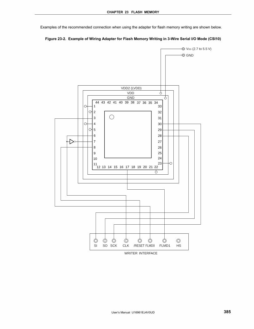
CHAPTER 23 FLASH MEMORY
User’s Manual U16961EJ4V0UD 385
Examples of the recommended connection when using the adapter for flash memory writing are shown below.
Figure 23-2. Example of Wiring Adapter for Flash Memory Writing in 3-Wire Serial I/O Mode (CSI10)
44 43 42 41 40 39 38
1312 14 15 16 17 18 19 20 21 2223
1
2
3
4
5
6
7
8
9
10
11
36 35 3433
32
31
30
29
28
27
26
25
37
24
GNDVDD
VDD2 (LVDD)
SI SO SCK CLK /RESET FLMD0 FLMD1 HS
WRITER INTERFACE
VDD (2.7 to 5.5 V)
GND
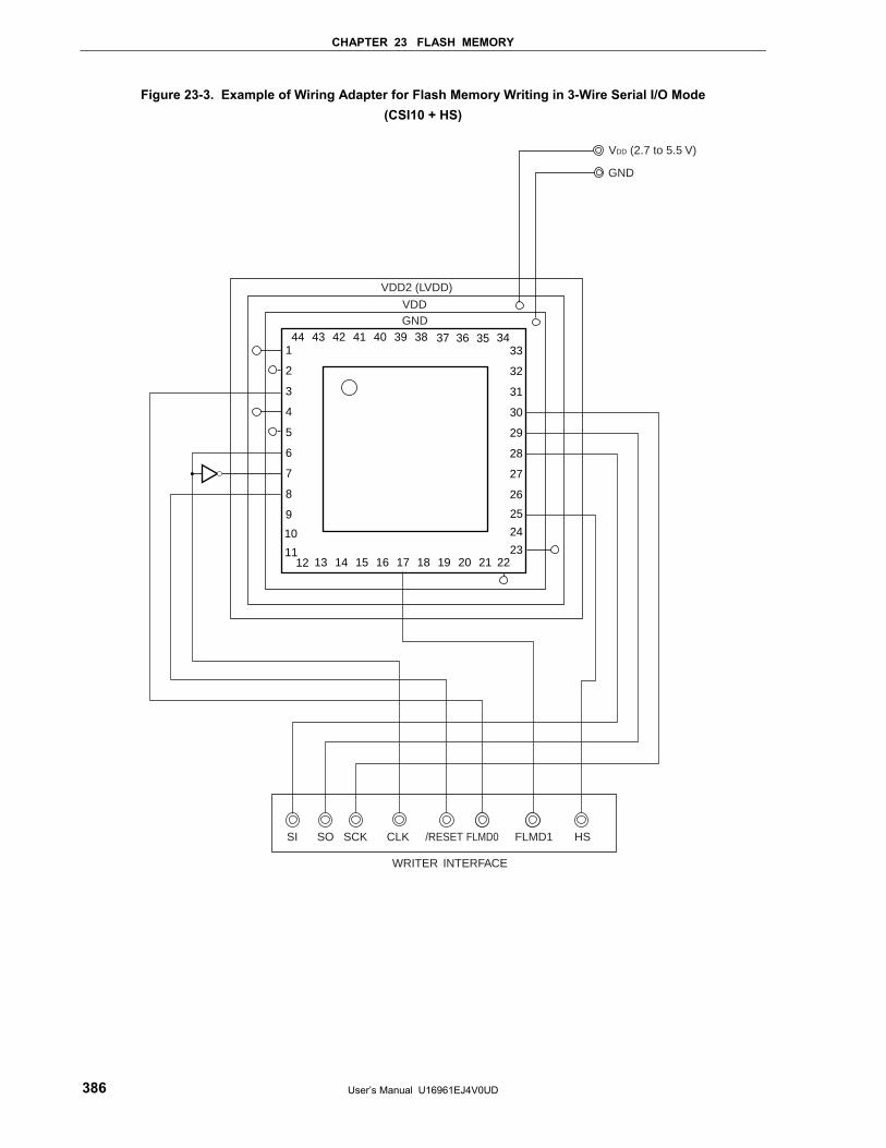
CHAPTER 23 FLASH MEMORY
User’s Manual U16961EJ4V0UD 386
Figure 23-3. Example of Wiring Adapter for Flash Memory Writing in 3-Wire Serial I/O Mode (CSI10 + HS)
44 43 42 41 40 39 38
1312 14 15 16 17 18 19 20 21 2223
1
2
3
4
5
6
7
8
9
10
11
36 35 3433
32
31
30
29
28
27
26
25
37
24
GNDVDD
GND
VDD2 (LVDD)
VDD (2.7 to 5.5 V)
WRITER INTERFACE
SI SO SCK CLK /RESET FLMD0 FLMD1 HS
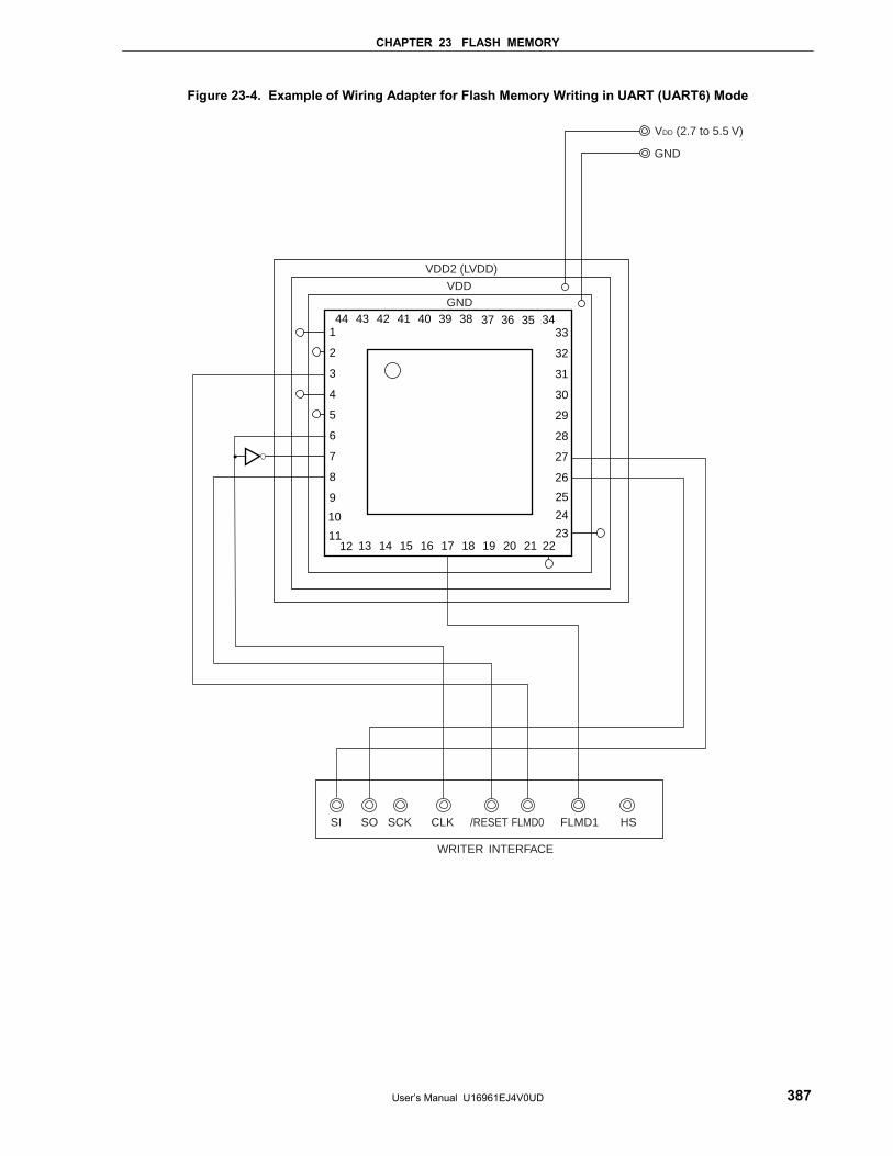
CHAPTER 23 FLASH MEMORY
User’s Manual U16961EJ4V0UD 387
Figure 23-4. Example of Wiring Adapter for Flash Memory Writing in UART (UART6) Mode
44 43 42 41 40 39 38
1312 14 15 16 17 18 19 20 21 2223
1
2
3
4
5
6
7
8
9
10
11
36 35 3433
32
31
30
29
28
27
26
25
37
24
GNDVDD
GND
VDD2 (LVDD)
VDD (2.7 to 5.5 V)
SI SO SCK CLK /RESET FLMD0 FLMD1 HS
WRITER INTERFACE
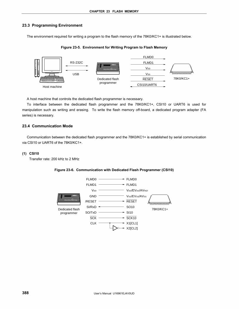
CHAPTER 23 FLASH MEMORY
User’s Manual U16961EJ4V0UD 388
23.3 Programming Environment
The environment required for writing a program to the flash memory of the 78K0/KC1+ is illustrated below.
Figure 23-5. Environment for Writing Program to Flash Memory
RS-232C
Host machine
78K0/KC1+
FLMD0
FLMD1
VDD
VSS
RESET
CSI10/UART6
Dedicated flashprogrammer
USB
PG-FP4 (Flash Pro4)
Cxxxxxx
Bxxxxx
Axxxx
XXX
YYY
XXXX
XXX
XXXX
XXXXXX
XX Y
YYY
STATVE
A host machine that controls the dedicated flash programmer is necessary. To interface between the dedicated flash programmer and the 78K0/KC1+, CSI10 or UART6 is used for
manipulation such as writing and erasing. To write the flash memory off-board, a dedicated program adapter (FA series) is necessary. 23.4 Communication Mode
Communication between the dedicated flash programmer and the 78K0/KC1+ is established by serial communication via CSI10 or UART6 of the 78K0/KC1+. (1) CSI10
Transfer rate: 200 kHz to 2 MHz
Figure 23-6. Communication with Dedicated Flash Programmer (CSI10)
78K0/KC1+
FLMD0FLMD0
Dedicated flashprogrammer
PG-FP4 (Flash Pro4)
Cxxxxxx
Bxxxxx
Axxxx
XXX
YYY
XXXX
XXX
XXXX
XXXXXX
XX Y
YYY
STATVE
FLMD1
VDD/EVDD/AVREF
VSS/EVSS/AVSS
RESET
SO10
SI10
SCK10
FLMD1
VDD
GND
/RESET
SI/RxD
SO/TxD
X1[CL1]CLK
X2[CL2]
SCK
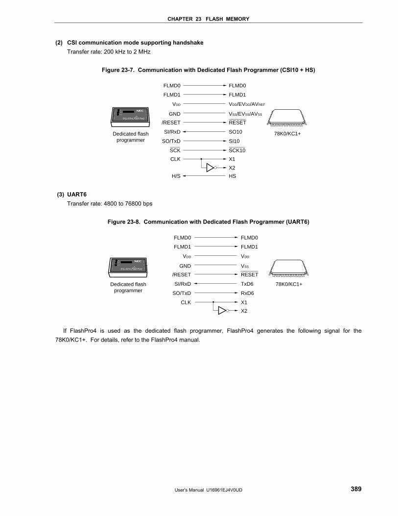
CHAPTER 23 FLASH MEMORY
User’s Manual U16961EJ4V0UD 389
(2) CSI communication mode supporting handshake Transfer rate: 200 kHz to 2 MHz
Figure 23-7. Communication with Dedicated Flash Programmer (CSI10 + HS)
78K0/KC1+
FLMD0FLMD0
Dedicated flashprogrammer
PG-FP4 (Flash Pro4)
Cxxxxxx
Bxxxxx
Axxxx
XXX
YYY
XXXX
XXX
XXXX
XXXXXX
XX Y
YYY
STATVE
FLMD1
RESET
SO10
SI10
SCK10
HS
FLMD1
VDD
GND
/RESET
SI/RxD
SO/TxD
SCK
X1CLK
X2
H/S
VDD/EVDD/AVREF
VSS/EVSS/AVSS
(3) UART6
Transfer rate: 4800 to 76800 bps
Figure 23-8. Communication with Dedicated Flash Programmer (UART6)
78K0/KC1+
FLMD0FLMD0
Dedicated flashprogrammer
PG-FP4 (Flash Pro4)
Cxxxxxx
Bxxxxx
Axxxx
XXX
YYY
XXXX
XXX
XXXX
XXXXXX
XX Y
YYY
STATVE
FLMD1
VDD
VSS
RESET
TxD6
RxD6
FLMD1
VDD
GND
/RESET
SI/RxD
SO/TxD
X1CLK
X2
If FlashPro4 is used as the dedicated flash programmer, FlashPro4 generates the following signal for the 78K0/KC1+. For details, refer to the FlashPro4 manual.
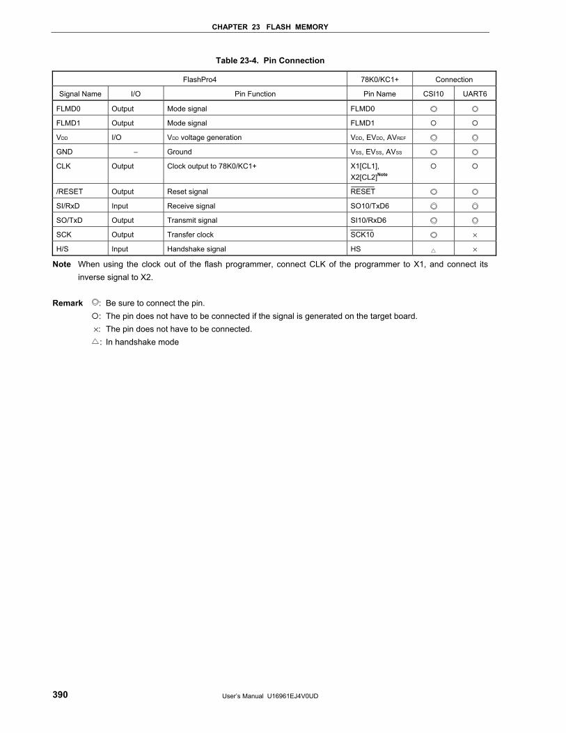
CHAPTER 23 FLASH MEMORY
User’s Manual U16961EJ4V0UD 390
Table 23-4. Pin Connection
FlashPro4 78K0/KC1+ Connection
Signal Name I/O Pin Function Pin Name CSI10 UART6
FLMD0 Output Mode signal FLMD0
FLMD1 Output Mode signal FLMD1
VDD I/O VDD voltage generation VDD, EVDD, AVREF
GND − Ground VSS, EVSS, AVSS
CLK Output Clock output to 78K0/KC1+ X1[CL1], X2[CL2]Note
/RESET Output Reset signal RESET
SI/RxD Input Receive signal SO10/TxD6
SO/TxD Output Transmit signal SI10/RxD6
SCK Output Transfer clock SCK10 ×
H/S Input Handshake signal HS ×
Note When using the clock out of the flash programmer, connect CLK of the programmer to X1, and connect its inverse signal to X2.
Remark : Be sure to connect the pin. : The pin does not have to be connected if the signal is generated on the target board. ×: The pin does not have to be connected. : In handshake mode
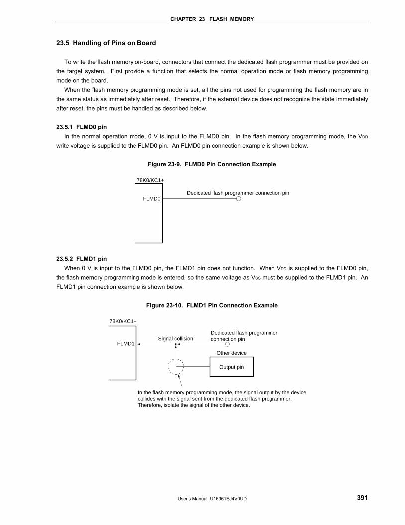
CHAPTER 23 FLASH MEMORY
User’s Manual U16961EJ4V0UD 391
23.5 Handling of Pins on Board
To write the flash memory on-board, connectors that connect the dedicated flash programmer must be provided on the target system. First provide a function that selects the normal operation mode or flash memory programming mode on the board.
When the flash memory programming mode is set, all the pins not used for programming the flash memory are in the same status as immediately after reset. Therefore, if the external device does not recognize the state immediately after reset, the pins must be handled as described below. 23.5.1 FLMD0 pin
In the normal operation mode, 0 V is input to the FLMD0 pin. In the flash memory programming mode, the VDD write voltage is supplied to the FLMD0 pin. An FLMD0 pin connection example is shown below.
Figure 23-9. FLMD0 Pin Connection Example
FLMD0Dedicated flash programmer connection pin
78K0/KC1+
23.5.2 FLMD1 pin
When 0 V is input to the FLMD0 pin, the FLMD1 pin does not function. When VDD is supplied to the FLMD0 pin, the flash memory programming mode is entered, so the same voltage as VSS must be supplied to the FLMD1 pin. An FLMD1 pin connection example is shown below.
Figure 23-10. FLMD1 Pin Connection Example
FLMD1Signal collision
Dedicated flash programmerconnection pin
Other device
Output pin
In the flash memory programming mode, the signal output by the device collides with the signal sent from the dedicated flash programmer. Therefore, isolate the signal of the other device.
78K0/KC1+
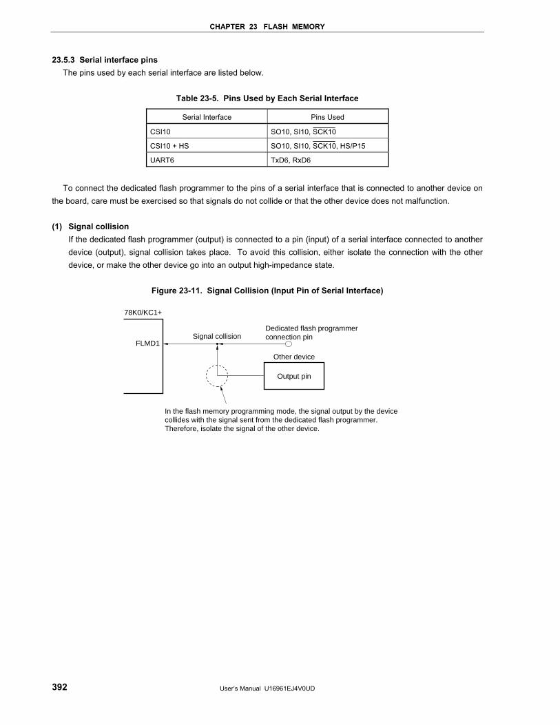
CHAPTER 23 FLASH MEMORY
User’s Manual U16961EJ4V0UD 392
23.5.3 Serial interface pins The pins used by each serial interface are listed below.
Table 23-5. Pins Used by Each Serial Interface
Serial Interface Pins Used
CSI10 SO10, SI10, SCK10
CSI10 + HS SO10, SI10, SCK10, HS/P15
UART6 TxD6, RxD6
To connect the dedicated flash programmer to the pins of a serial interface that is connected to another device on
the board, care must be exercised so that signals do not collide or that the other device does not malfunction. (1) Signal collision
If the dedicated flash programmer (output) is connected to a pin (input) of a serial interface connected to another device (output), signal collision takes place. To avoid this collision, either isolate the connection with the other device, or make the other device go into an output high-impedance state.
Figure 23-11. Signal Collision (Input Pin of Serial Interface)
FLMD1Signal collision
Dedicated flash programmerconnection pin
Other device
Output pin
In the flash memory programming mode, the signal output by the device collides with the signal sent from the dedicated flash programmer. Therefore, isolate the signal of the other device.
78K0/KC1+
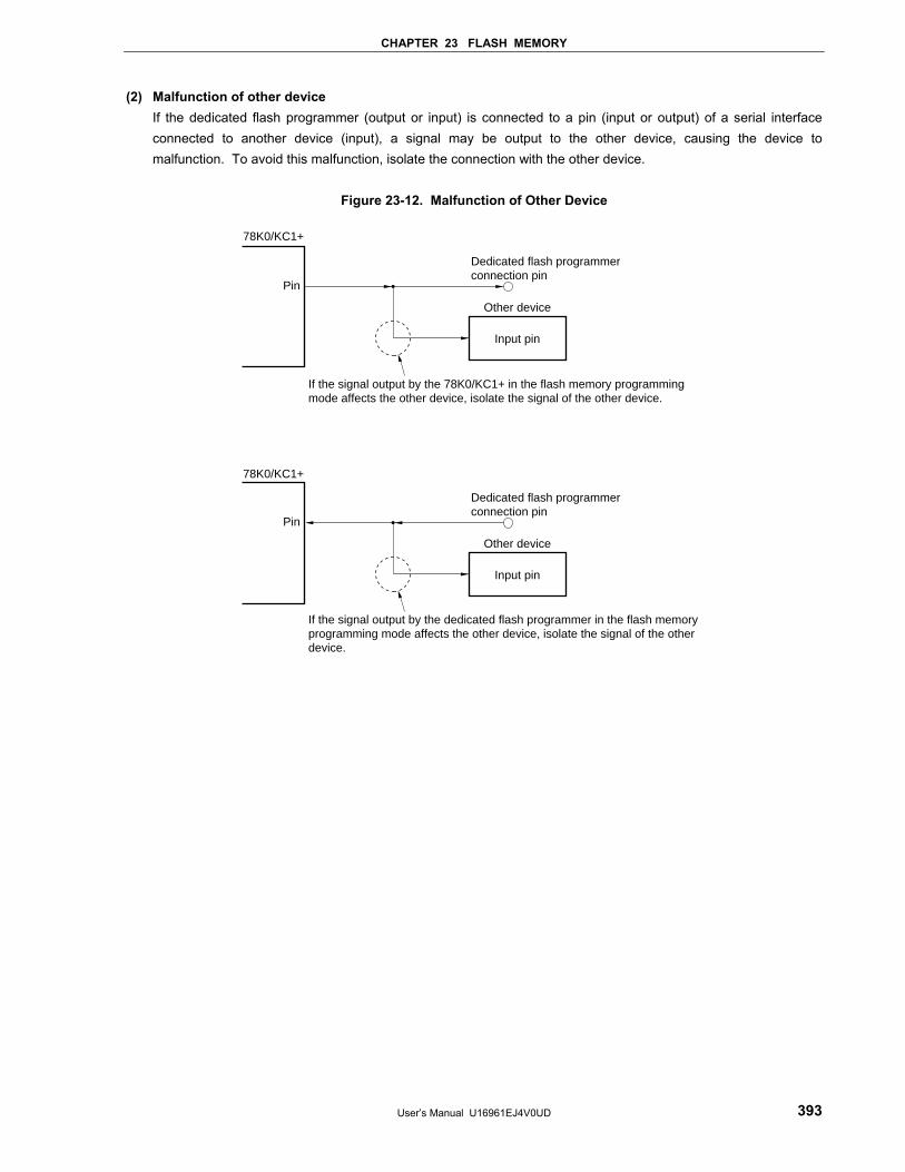
CHAPTER 23 FLASH MEMORY
User’s Manual U16961EJ4V0UD 393
(2) Malfunction of other device If the dedicated flash programmer (output or input) is connected to a pin (input or output) of a serial interface connected to another device (input), a signal may be output to the other device, causing the device to malfunction. To avoid this malfunction, isolate the connection with the other device.
Figure 23-12. Malfunction of Other Device
Pin
Dedicated flash programmer connection pin
Other device
Input pin
If the signal output by the 78K0/KC1+ in the flash memory programming mode affects the other device, isolate the signal of the other device.
Pin
Dedicated flash programmer connection pin
Other device
Input pin
If the signal output by the dedicated flash programmer in the flash memory programming mode affects the other device, isolate the signal of the other device.
78K0/KC1+
78K0/KC1+
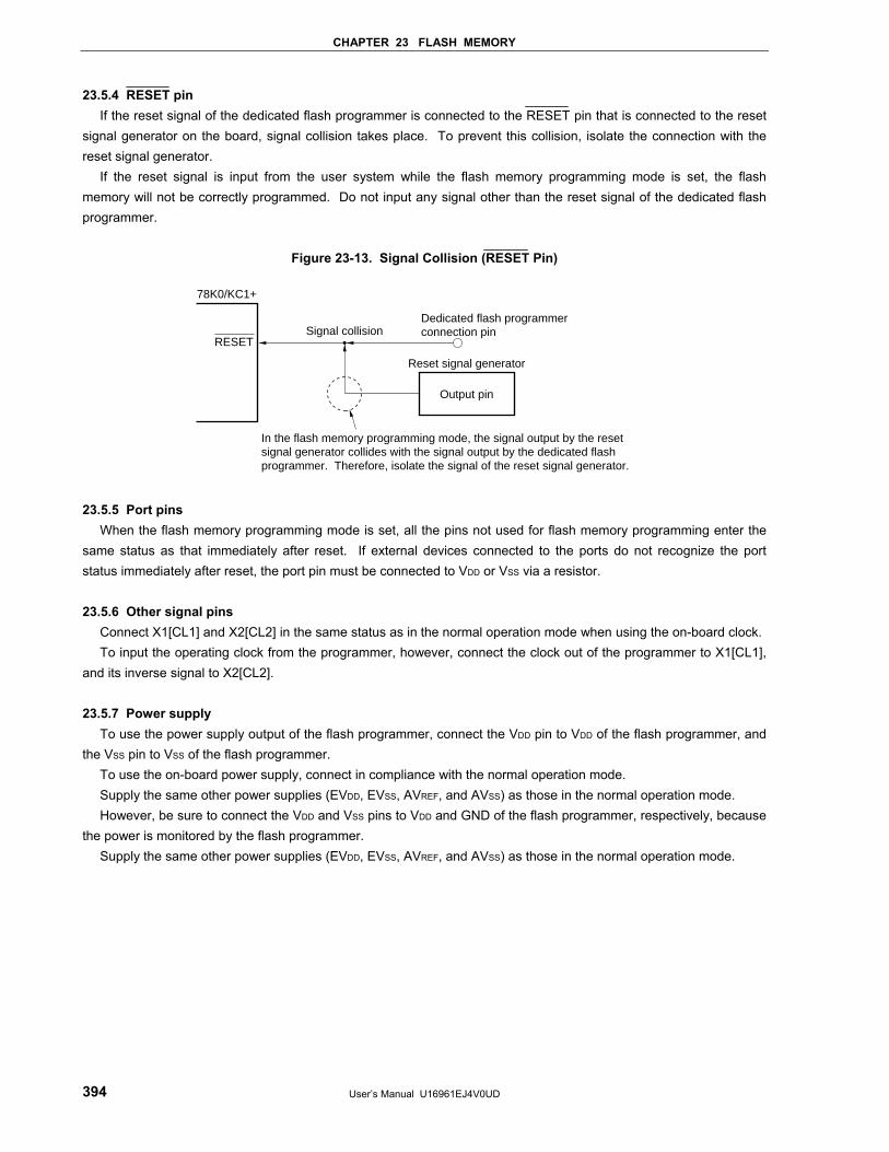
CHAPTER 23 FLASH MEMORY
User’s Manual U16961EJ4V0UD 394
23.5.4 RESET pin If the reset signal of the dedicated flash programmer is connected to the RESET pin that is connected to the reset
signal generator on the board, signal collision takes place. To prevent this collision, isolate the connection with the reset signal generator.
If the reset signal is input from the user system while the flash memory programming mode is set, the flash memory will not be correctly programmed. Do not input any signal other than the reset signal of the dedicated flash programmer.
Figure 23-13. Signal Collision (RESET Pin)
RESET
Dedicated flash programmer connection pin
Reset signal generator
Signal collision
Output pin
In the flash memory programming mode, the signal output by the reset signal generator collides with the signal output by the dedicated flash programmer. Therefore, isolate the signal of the reset signal generator.
78K0/KC1+
23.5.5 Port pins
When the flash memory programming mode is set, all the pins not used for flash memory programming enter the same status as that immediately after reset. If external devices connected to the ports do not recognize the port status immediately after reset, the port pin must be connected to VDD or VSS via a resistor. 23.5.6 Other signal pins
Connect X1[CL1] and X2[CL2] in the same status as in the normal operation mode when using the on-board clock. To input the operating clock from the programmer, however, connect the clock out of the programmer to X1[CL1],
and its inverse signal to X2[CL2]. 23.5.7 Power supply
To use the power supply output of the flash programmer, connect the VDD pin to VDD of the flash programmer, and the VSS pin to VSS of the flash programmer.
To use the on-board power supply, connect in compliance with the normal operation mode. Supply the same other power supplies (EVDD, EVSS, AVREF, and AVSS) as those in the normal operation mode. However, be sure to connect the VDD and VSS pins to VDD and GND of the flash programmer, respectively, because
the power is monitored by the flash programmer. Supply the same other power supplies (EVDD, EVSS, AVREF, and AVSS) as those in the normal operation mode.
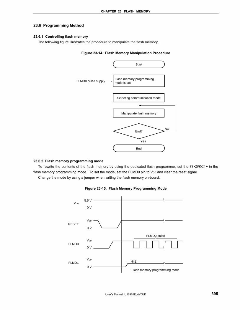
CHAPTER 23 FLASH MEMORY
User’s Manual U16961EJ4V0UD 395
23.6 Programming Method 23.6.1 Controlling flash memory
The following figure illustrates the procedure to manipulate the flash memory.
Figure 23-14. Flash Memory Manipulation Procedure
Start
Selecting communication mode
Manipulate flash memory
End?
Yes
FLMD0 pulse supply
No
End
Flash memory programming mode is set
23.6.2 Flash memory programming mode
To rewrite the contents of the flash memory by using the dedicated flash programmer, set the 78K0/KC1+ in the flash memory programming mode. To set the mode, set the FLMD0 pin to VDD and clear the reset signal.
Change the mode by using a jumper when writing the flash memory on-board.
Figure 23-15. Flash Memory Programming Mode
VDD
RESET
5.5 V
0 V
VDD
0 V
Flash memory programming mode
VDD
0 V
FLMD0
FLMD0 pulse
Hi-Z
VDD
0 V
FLMD1
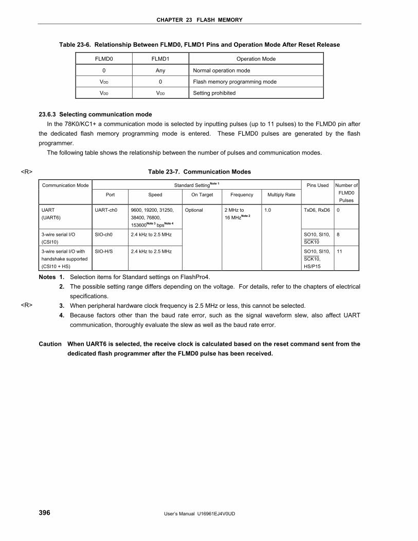
CHAPTER 23 FLASH MEMORY
User’s Manual U16961EJ4V0UD 396
Table 23-6. Relationship Between FLMD0, FLMD1 Pins and Operation Mode After Reset Release
FLMD0 FLMD1 Operation Mode
0 Any Normal operation mode
VDD 0 Flash memory programming mode
VDD VDD Setting prohibited
23.6.3 Selecting communication mode
In the 78K0/KC1+ a communication mode is selected by inputting pulses (up to 11 pulses) to the FLMD0 pin after the dedicated flash memory programming mode is entered. These FLMD0 pulses are generated by the flash programmer.
The following table shows the relationship between the number of pulses and communication modes.
Table 23-7. Communication Modes
Standard SettingNote 1 Communication Mode
Port Speed On Target Frequency Multiply Rate
Pins Used Number of FLMD0
Pulses
UART (UART6)
UART-ch0 9600, 19200, 31250, 38400, 76800, 153600Note 3 bpsNote 4
TxD6, RxD6 0
3-wire serial I/O (CSI10)
SIO-ch0 2.4 kHz to 2.5 MHz SO10, SI10, SCK10
8
3-wire serial I/O with handshake supported (CSI10 + HS)
SIO-H/S 2.4 kHz to 2.5 MHz
Optional 2 MHz to 16 MHzNote 2
1.0
SO10, SI10, SCK10, HS/P15
11
Notes 1. Selection items for Standard settings on FlashPro4. 2. The possible setting range differs depending on the voltage. For details, refer to the chapters of electrical
specifications. 3. When peripheral hardware clock frequency is 2.5 MHz or less, this cannot be selected. 4. Because factors other than the baud rate error, such as the signal waveform slew, also affect UART
communication, thoroughly evaluate the slew as well as the baud rate error. Caution When UART6 is selected, the receive clock is calculated based on the reset command sent from the
dedicated flash programmer after the FLMD0 pulse has been received.
<R>
<R>
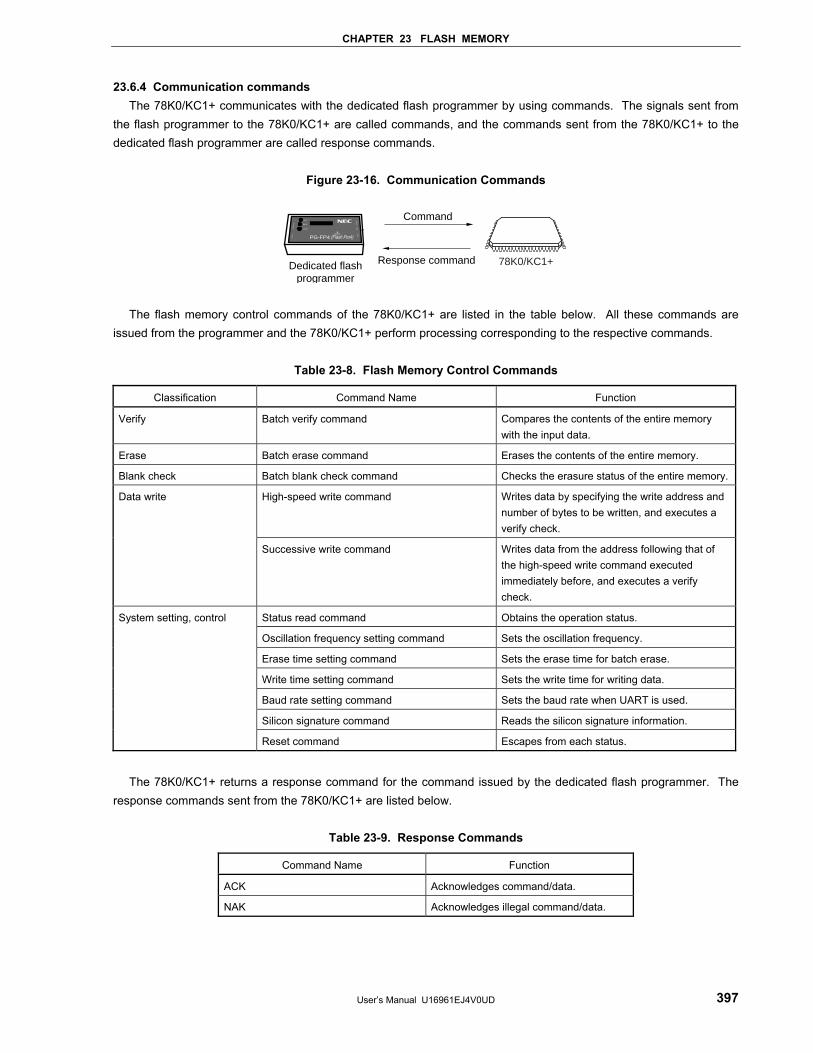
CHAPTER 23 FLASH MEMORY
User’s Manual U16961EJ4V0UD 397
23.6.4 Communication commands The 78K0/KC1+ communicates with the dedicated flash programmer by using commands. The signals sent from
the flash programmer to the 78K0/KC1+ are called commands, and the commands sent from the 78K0/KC1+ to the dedicated flash programmer are called response commands.
Figure 23-16. Communication Commands
78K0/KC1+
Command
Response commandDedicated flashprogrammer
PG-FP4 (Flash Pro4)
Cxxxxxx
Bxxxxx
Axxxx
XXX
YYY
XXXX
XXX
XXXX
XXXXXX
XX Y
YYY
STATVE
The flash memory control commands of the 78K0/KC1+ are listed in the table below. All these commands are issued from the programmer and the 78K0/KC1+ perform processing corresponding to the respective commands.
Table 23-8. Flash Memory Control Commands
Classification Command Name Function
Verify Batch verify command Compares the contents of the entire memory with the input data.
Erase Batch erase command Erases the contents of the entire memory.
Blank check Batch blank check command Checks the erasure status of the entire memory.
High-speed write command Writes data by specifying the write address and number of bytes to be written, and executes a verify check.
Data write
Successive write command Writes data from the address following that of the high-speed write command executed immediately before, and executes a verify check.
Status read command Obtains the operation status.
Oscillation frequency setting command Sets the oscillation frequency.
Erase time setting command Sets the erase time for batch erase.
Write time setting command Sets the write time for writing data.
Baud rate setting command Sets the baud rate when UART is used.
Silicon signature command Reads the silicon signature information.
System setting, control
Reset command Escapes from each status.
The 78K0/KC1+ returns a response command for the command issued by the dedicated flash programmer. The
response commands sent from the 78K0/KC1+ are listed below.
Table 23-9. Response Commands
Command Name Function
ACK Acknowledges command/data.
NAK Acknowledges illegal command/data.
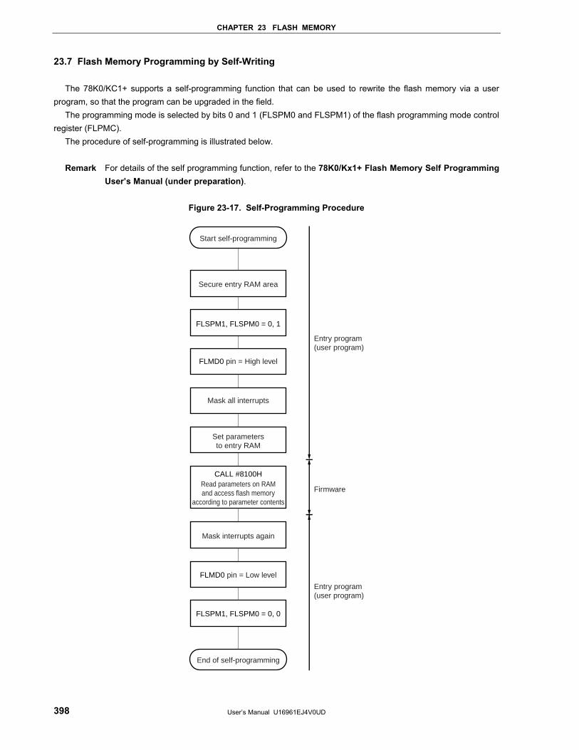
CHAPTER 23 FLASH MEMORY
User’s Manual U16961EJ4V0UD 398
23.7 Flash Memory Programming by Self-Writing
The 78K0/KC1+ supports a self-programming function that can be used to rewrite the flash memory via a user program, so that the program can be upgraded in the field.
The programming mode is selected by bits 0 and 1 (FLSPM0 and FLSPM1) of the flash programming mode control register (FLPMC).
The procedure of self-programming is illustrated below.
Remark For details of the self programming function, refer to the 78K0/Kx1+ Flash Memory Self Programming User’s Manual (under preparation).
Figure 23-17. Self-Programming Procedure
Mask interrupts again
FLSPM1, FLSPM0 = 0, 1
Secure entry RAM area
Mask all interrupts
FLMD0 pin = High level
CALL #8100H
Set parametersto entry RAM
Start self-programming
Read parameters on RAMand access flash memory
according to parameter contents
FLMD0 pin = Low level
FLSPM1, FLSPM0 = 0, 0
End of self-programming
Entry program (user program)
Firmware
Entry program (user program)
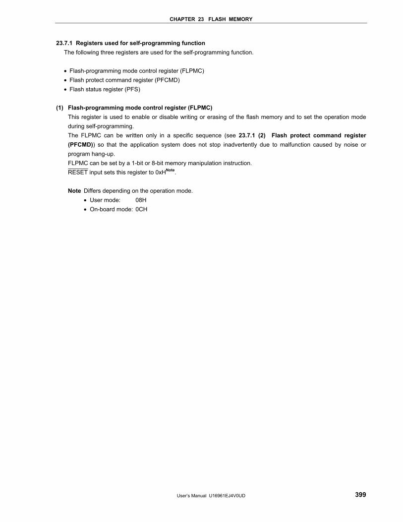
CHAPTER 23 FLASH MEMORY
User’s Manual U16961EJ4V0UD 399
23.7.1 Registers used for self-programming function The following three registers are used for the self-programming function.
• Flash-programming mode control register (FLPMC) • Flash protect command register (PFCMD) • Flash status register (PFS)
(1) Flash-programming mode control register (FLPMC)
This register is used to enable or disable writing or erasing of the flash memory and to set the operation mode during self-programming. The FLPMC can be written only in a specific sequence (see 23.7.1 (2) Flash protect command register (PFCMD)) so that the application system does not stop inadvertently due to malfunction caused by noise or program hang-up. FLPMC can be set by a 1-bit or 8-bit memory manipulation instruction. RESET input sets this register to 0xHNote.
Note Differs depending on the operation mode. • User mode: 08H • On-board mode: 0CH
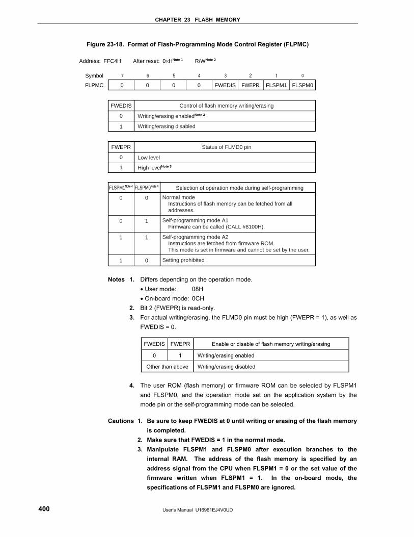
CHAPTER 23 FLASH MEMORY
User’s Manual U16961EJ4V0UD 400
Figure 23-18. Format of Flash-Programming Mode Control Register (FLPMC)
0
Symbol
FLPMC 0 0 0 FWEDIS FWEPR FLSPM1 FLSPM0
Address: FFC4H After reset: 0×HNote 1 R/WNote 2
Selection of operation mode during self-programming
Normal modeInstructions of flash memory can be fetched from all addresses.
Self-programming mode A1Firmware can be called (CALL #8100H).
Self-programming mode A2Instructions are fetched from firmware ROM.This mode is set in firmware and cannot be set by the user.
Setting prohibited
FLSPM1Note 4
0
0
1
1
FLSPM0Note 4
0
1
1
0
FWEDIS
0
Control of flash memory writing/erasing
Writing/erasing enabledNote 3
Writing/erasing disabled1
Status of FLMD0 pin
Low level
High levelNote 3
FWEPR
0
1
Notes 1. Differs depending on the operation mode. • User mode: 08H • On-board mode: 0CH 2. Bit 2 (FWEPR) is read-only. 3. For actual writing/erasing, the FLMD0 pin must be high (FWEPR = 1), as well as
FWEDIS = 0.
FWEDIS FWEPR Enable or disable of flash memory writing/erasing
0 1 Writing/erasing enabled
Other than above Writing/erasing disabled
4. The user ROM (flash memory) or firmware ROM can be selected by FLSPM1
and FLSPM0, and the operation mode set on the application system by the mode pin or the self-programming mode can be selected.
Cautions 1. Be sure to keep FWEDIS at 0 until writing or erasing of the flash memory
is completed. 2. Make sure that FWEDIS = 1 in the normal mode. 3. Manipulate FLSPM1 and FLSPM0 after execution branches to the
internal RAM. The address of the flash memory is specified by an address signal from the CPU when FLSPM1 = 0 or the set value of the firmware written when FLSPM1 = 1. In the on-board mode, the specifications of FLSPM1 and FLSPM0 are ignored.
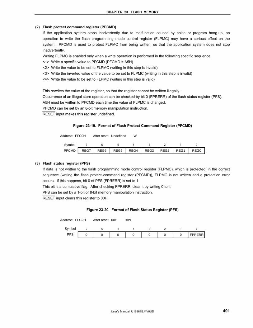
CHAPTER 23 FLASH MEMORY
User’s Manual U16961EJ4V0UD 401
(2) Flash protect command register (PFCMD) If the application system stops inadvertently due to malfunction caused by noise or program hang-up, an operation to write the flash programming mode control register (FLPMC) may have a serious effect on the system. PFCMD is used to protect FLPMC from being written, so that the application system does not stop inadvertently. Writing FLPMC is enabled only when a write operation is performed in the following specific sequence. <1> Write a specific value to PFCMD (PFCMD = A5H) <2> Write the value to be set to FLPMC (writing in this step is invalid) <3> Write the inverted value of the value to be set to FLPMC (writing in this step is invalid) <4> Write the value to be set to FLPMC (writing in this step is valid)
This rewrites the value of the register, so that the register cannot be written illegally. Occurrence of an illegal store operation can be checked by bit 0 (FPRERR) of the flash status register (PFS). A5H must be written to PFCMD each time the value of FLPMC is changed. PFCMD can be set by an 8-bit memory manipulation instruction. RESET input makes this register undefined.
Figure 23-19. Format of Flash Protect Command Register (PFCMD)
REG7
Symbol
PFCMD REG6 REG5 REG4 REG3 REG2 REG1 REG0
Address: FFC0H After reset: Undefined W
(3) Flash status register (PFS)
If data is not written to the flash programming mode control register (FLPMC), which is protected, in the correct sequence (writing the flash protect command register (PFCMD)), FLPMC is not written and a protection error occurs. If this happens, bit 0 of PFS (FPRERR) is set to 1. This bit is a cumulative flag. After checking FPRERR, clear it by writing 0 to it. PFS can be set by a 1-bit or 8-bit memory manipulation instruction. RESET input clears this register to 00H.
Figure 23-20. Format of Flash Status Register (PFS)
0
Symbol
PFS 0 0 0 0 0 0 FPRERR
Address: FFC2H After reset: 00H R/W
CHAPTER 23 FLASH MEMORY
User’s Manual U16961EJ4V0UD 402
The operating conditions of the FPRERR flag are as follows.
<Setting conditions> • If PFCMD is written when the store instruction operation recently performed on a peripheral register is not to
write a specific value (A5H) to PFCMD • If the first store instruction operation after <1> is on a peripheral register other than FLPMC • If the first store instruction operation after <2> is on a peripheral register other than FLPMC • If a value other than the inverted value of the value to be set to FLPMC is written by the first store instruction
after <2> • If the first store instruction operation after <3> is on a peripheral register other than FLPMC • If a value other than the value to be set to FLPMC (value written in <2>) is written by the first store instruction
after <3>
Remark The numbers in angle brackets above correspond to the those in (2) Flash protect command register (PFCMD).
<Reset conditions> • If 0 is written to the FPRERR flag • If RESET is input
<Example of description in specific sequence> To write 05H to FLPMC
MOV PFCMD, #0A5H ; Writes A5H to PFCMD. MOV FLPMC, #05H ; Writes 05H to FLPMC. MOV FLPMC, #0FAH ; Writes 0FAH (inverted value of 05H) to FLPMC. MOV FLPMC, #05H ; Writes 05H to FLPMC.
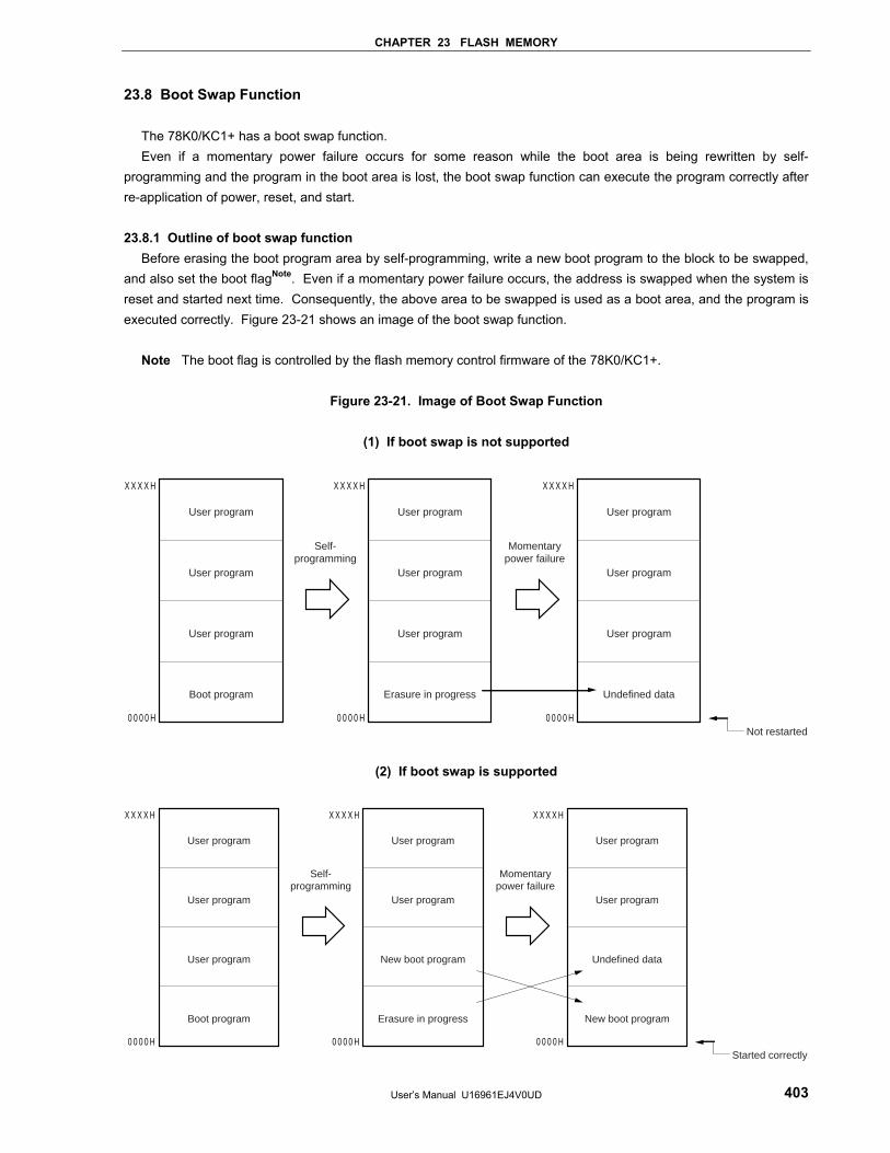
CHAPTER 23 FLASH MEMORY
User’s Manual U16961EJ4V0UD 403
23.8 Boot Swap Function
The 78K0/KC1+ has a boot swap function. Even if a momentary power failure occurs for some reason while the boot area is being rewritten by self-
programming and the program in the boot area is lost, the boot swap function can execute the program correctly after re-application of power, reset, and start. 23.8.1 Outline of boot swap function
Before erasing the boot program area by self-programming, write a new boot program to the block to be swapped, and also set the boot flagNote. Even if a momentary power failure occurs, the address is swapped when the system is reset and started next time. Consequently, the above area to be swapped is used as a boot area, and the program is executed correctly. Figure 23-21 shows an image of the boot swap function.
Note The boot flag is controlled by the flash memory control firmware of the 78K0/KC1+.
Figure 23-21. Image of Boot Swap Function
(1) If boot swap is not supported
User program
User program
User program
Boot program
X X X X H
0 0 0 0 H
User program
User program
User program
Erasure in progress
X X X X H
0 0 0 0 H
User program
User program
User program
Undefined data
X X X X H
0 0 0 0 H
Self-programming
Momentarypower failure
Not restarted
(2) If boot swap is supported
User program
User program
User program
Boot program
X X X X H
0 0 0 0 H
User program
User program
New boot program
Erasure in progress
X X X X H
0 0 0 0 H
User program
User program
Undefined data
New boot program
X X X X H
0 0 0 0 H
Self-programming
Momentarypower failure
Started correctly
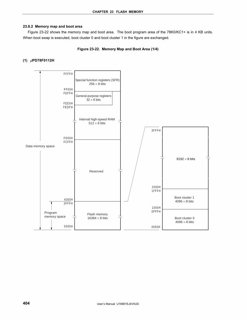
CHAPTER 23 FLASH MEMORY
User’s Manual U16961EJ4V0UD 404
23.8.2 Memory map and boot area Figure 23-22 shows the memory map and boot area. The boot program area of the 78K0/KC1+ is in 4 KB units.
When boot swap is executed, boot cluster 0 and boot cluster 1 in the figure are exchanged.
Figure 23-22. Memory Map and Boot Area (1/4) (1) μPD78F0112H
F F 0 0 HF E F F H
F E E 0 HF E D F H
F D 0 0 HF C F F H
4 0 0 0 H3 F F F H
1 0 0 0 H0 F F F H
2 0 0 0 H1 F F F H
Boot cluster 04096 × 8 bits
Boot cluster 14096 × 8 bits
8192 × 8 bits
Special function registers (SFR)256 × 8 bits
General-purpose registers32 × 8 bits
Flash memory16384 × 8 bits
Internal high-speed RAM512 × 8 bits
Reserved
Data memory space
Program memory space
0 0 0 0 H0 0 0 0 H
3 F F F H
F F F F H
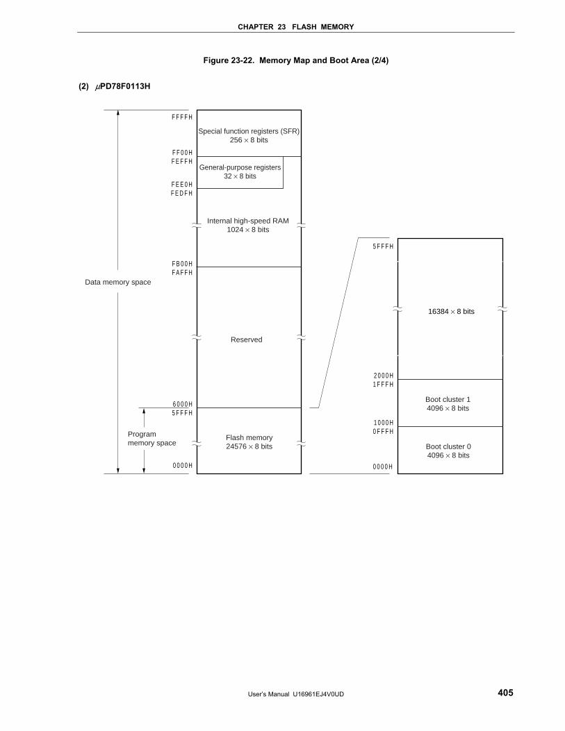
CHAPTER 23 FLASH MEMORY
User’s Manual U16961EJ4V0UD 405
Figure 23-22. Memory Map and Boot Area (2/4) (2) μPD78F0113H
F F 0 0 HF E F F H
F E E 0 HF E D F H
F B 0 0 HF A F F H
6 0 0 0 H5 F F F H
1 0 0 0 H0 F F F H
2 0 0 0 H1 F F F H
Boot cluster 04096 × 8 bits
Boot cluster 14096 × 8 bits
16384 × 8 bits
Special function registers (SFR)256 × 8 bits
General-purpose registers32 × 8 bits
Flash memory24576 × 8 bits
Internal high-speed RAM1024 × 8 bits
Reserved
Data memory space
Program memory space
0 0 0 0 H0 0 0 0 H
5 F F F H
F F F F H
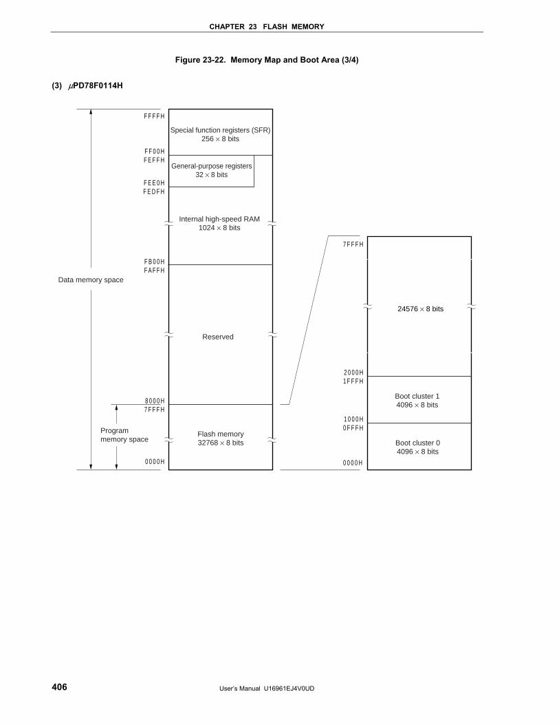
CHAPTER 23 FLASH MEMORY
User’s Manual U16961EJ4V0UD 406
Figure 23-22. Memory Map and Boot Area (3/4) (3) μPD78F0114H
F F 0 0 HF E F F H
F E E 0 HF E D F H
F B 0 0 HF A F F H
8 0 0 0 H7 F F F H
1 0 0 0 H0 F F F H
2 0 0 0 H1 F F F H
Boot cluster 04096 × 8 bits
Boot cluster 14096 × 8 bits
24576 × 8 bits
Special function registers (SFR)256 × 8 bits
General-purpose registers32 × 8 bits
Flash memory32768 × 8 bits
Internal high-speed RAM1024 × 8 bits
Reserved
Data memory space
Program memory space
0 0 0 0 H0 0 0 0 H
7 F F F H
F F F F H
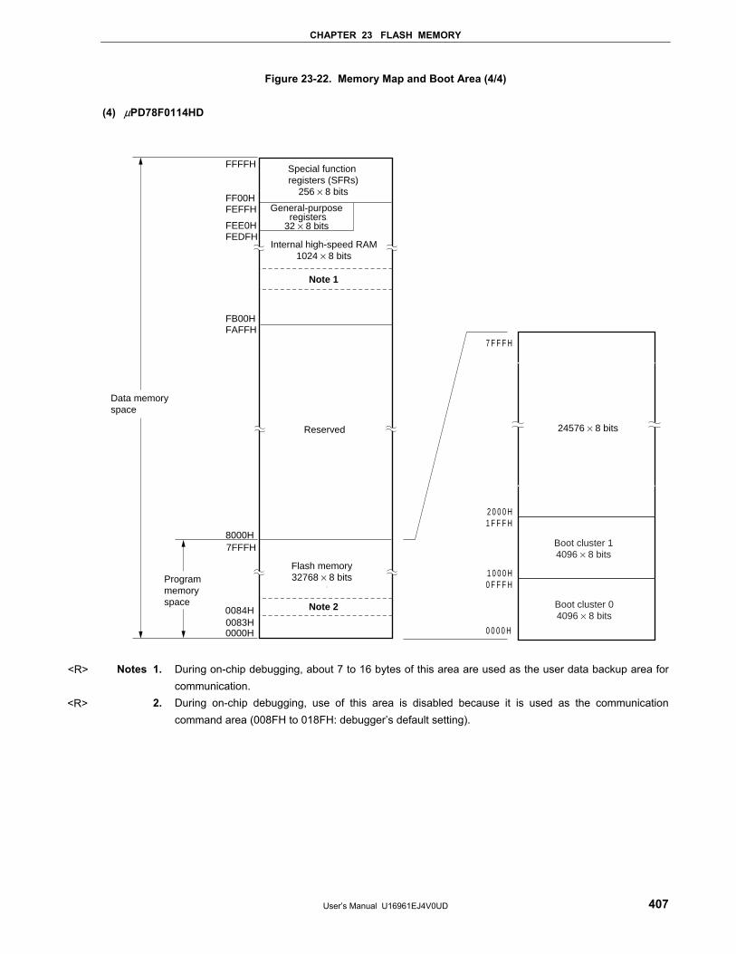
CHAPTER 23 FLASH MEMORY
User’s Manual U16961EJ4V0UD 407
Figure 23-22. Memory Map and Boot Area (4/4) (4) μPD78F0114HD
1 0 0 0 H0 F F F H
2 0 0 0 H1 F F F H
Boot cluster 04096 × 8 bits
Boot cluster 14096 × 8 bits
24576 × 8 bits
0 0 0 0 H
7 F F F H
0000H
Data memory space
General-purpose registers32 × 8 bits
Flash memory32768 × 8 bitsProgram
memoryspace
8000H7FFFH
FEE0HFEDFH
FF00HFEFFH
FFFFH
Internal high-speed RAM1024 × 8 bits
Special function registers (SFRs)
256 × 8 bits
Reserved
FB00HFAFFH
Note 2
0083H0084H
Note 1
Notes 1. During on-chip debugging, about 7 to 16 bytes of this area are used as the user data backup area for communication.
2. During on-chip debugging, use of this area is disabled because it is used as the communication command area (008FH to 018FH: debugger’s default setting).
<R>
<R>
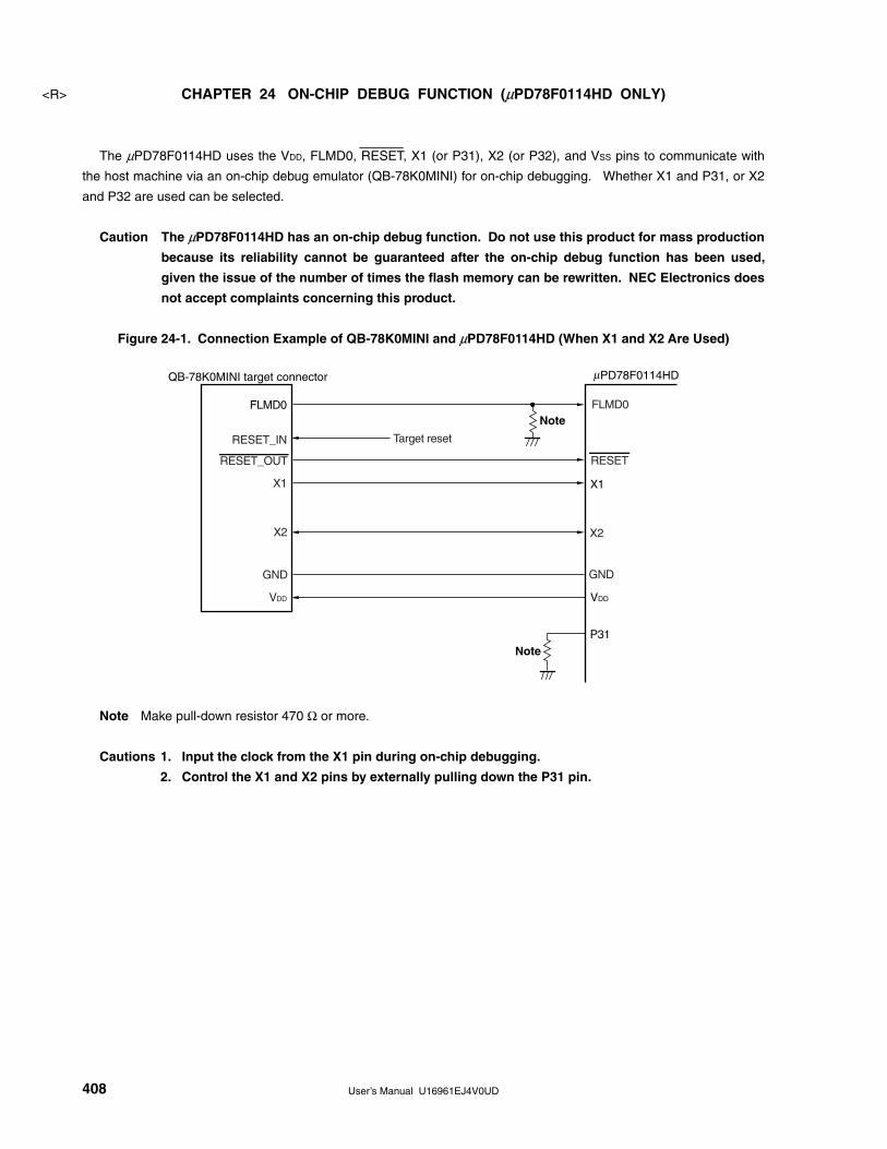
User’s Manual U16961EJ4V0UD 408
CHAPTER 24 ON-CHIP DEBUG FUNCTION (µPD78F0114HD ONLY)
The µPD78F0114HD uses the VDD, FLMD0, RESET, X1 (or P31), X2 (or P32), and VSS pins to communicate with
the host machine via an on-chip debug emulator (QB-78K0MINI) for on-chip debugging. Whether X1 and P31, or X2
and P32 are used can be selected.
Caution The µPD78F0114HD has an on-chip debug function. Do not use this product for mass production
because its reliability cannot be guaranteed after the on-chip debug function has been used,
given the issue of the number of times the flash memory can be rewritten. NEC Electronics does
not accept complaints concerning this product.
Figure 24-1. Connection Example of QB-78K0MINI and µPD78F0114HD (When X1 and X2 Are Used)
VDD
PD78F0114HD
P31
FLMD0
X1
X2
Target resetRESET_IN
X2
X1
FLMD0
RESET
VDD
RESET_OUT
GND
QB-78K0MINI target connector
GND
Note
Note
µ
Note Make pull-down resistor 470 Ω or more.
Cautions 1. Input the clock from the X1 pin during on-chip debugging.
2. Control the X1 and X2 pins by externally pulling down the P31 pin.
<R>
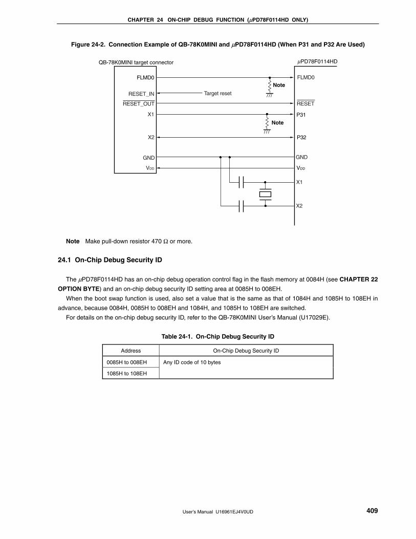
CHAPTER 24 ON-CHIP DEBUG FUNCTION (µPD78F0114HD ONLY)
User’s Manual U16961EJ4V0UD 409
Figure 24-2. Connection Example of QB-78K0MINI and µPD78F0114HD (When P31 and P32 Are Used)
QB-78K0MINI target connector
VDD
P32
FLMD0
P31
X2
Target resetRESET_IN
X2
X1
FLMD0
RESET
VDD
RESET_OUT
GND
X1
GND
Note
Note
PD78F0114HDµ
Note Make pull-down resistor 470 Ω or more.
24.1 On-Chip Debug Security ID
The µPD78F0114HD has an on-chip debug operation control flag in the flash memory at 0084H (see CHAPTER 22
OPTION BYTE) and an on-chip debug security ID setting area at 0085H to 008EH.
When the boot swap function is used, also set a value that is the same as that of 1084H and 1085H to 108EH in
advance, because 0084H, 0085H to 008EH and 1084H, and 1085H to 108EH are switched.
For details on the on-chip debug security ID, refer to the QB-78K0MINI User’s Manual (U17029E).
Table 24-1. On-Chip Debug Security ID
Address On-Chip Debug Security ID
0085H to 008EH
1085H to 108EH
Any ID code of 10 bytes
User’s Manual U16961EJ4V0UD 410
CHAPTER 25 INSTRUCTION SET
This chapter lists each instruction set of the 78K0/KC1+ in table form. For details of each operation and operation
code, refer to the separate document 78K/0 Series Instructions User’s Manual (U12326E).
25.1 Conventions Used in Operation List
25.1.1 Operand identifiers and specification methods
Operands are written in the “Operand” column of each instruction in accordance with the specification method of
the instruction operand identifier (refer to the assembler specifications for details). When there are two or more
methods, select one of them. Uppercase letters and the symbols #, !, $ and [ ] are keywords and must be written as
they are. Each symbol has the following meaning.
• #: Immediate data specification
• !: Absolute address specification
• $: Relative address specification
• [ ]: Indirect address specification
In the case of immediate data, describe an appropriate numeric value or a label. When using a label, be sure to
write the #, !, $, and [ ] symbols.
For operand register identifiers r and rp, either function names (X, A, C, etc.) or absolute names (names in
parentheses in the table below, R0, R1, R2, etc.) can be used for specification.
Table 25-1. Operand Identifiers and Specification Methods
Identifier Specification Method
r
rp
sfr
sfrp
X (R0), A (R1), C (R2), B (R3), E (R4), D (R5), L (R6), H (R7)
AX (RP0), BC (RP1), DE (RP2), HL (RP3)
Special function register symbolNote
Special function register symbol (16-bit manipulatable register even addresses only)Note
saddr
saddrp
FE20H to FF1FH Immediate data or labels
FE20H to FF1FH Immediate data or labels (even address only)
addr16
addr11
addr5
0000H to FFFFH Immediate data or labels
(Only even addresses for 16-bit data transfer instructions)
0800H to 0FFFH Immediate data or labels
0040H to 007FH Immediate data or labels (even address only)
word
byte
bit
16-bit immediate data or label
8-bit immediate data or label
3-bit immediate data or label
RBn RB0 to RB3
Note Addresses from FFD0H to FFDFH cannot be accessed with these operands.
Remark For special function register symbols, refer to Table 3-5 Special Function Register List.
CHAPTER 25 INSTRUCTION SET
User’s Manual U16961EJ4V0UD 411
25.1.2 Description of operation column
A: A register; 8-bit accumulator
X: X register
B: B register
C: C register
D: D register
E: E register
H: H register
L: L register
AX: AX register pair; 16-bit accumulator
BC: BC register pair
DE: DE register pair
HL: HL register pair
PC: Program counter
SP: Stack pointer
PSW: Program status word
CY: Carry flag
AC: Auxiliary carry flag
Z: Zero flag
RBS: Register bank select flag
IE: Interrupt request enable flag
( ): Memory contents indicated by address or register contents in parentheses
XH, XL: Higher 8 bits and lower 8 bits of 16-bit register
∧: Logical product (AND)
∨: Logical sum (OR)
∨: Exclusive logical sum (exclusive OR) : Inverted data
addr16: 16-bit immediate data or label
jdisp8: Signed 8-bit data (displacement value)
25.1.3 Description of flag operation column
(Blank): Not affected
0: Cleared to 0
1: Set to 1
×: Set/cleared according to the result
R: Previously saved value is restored
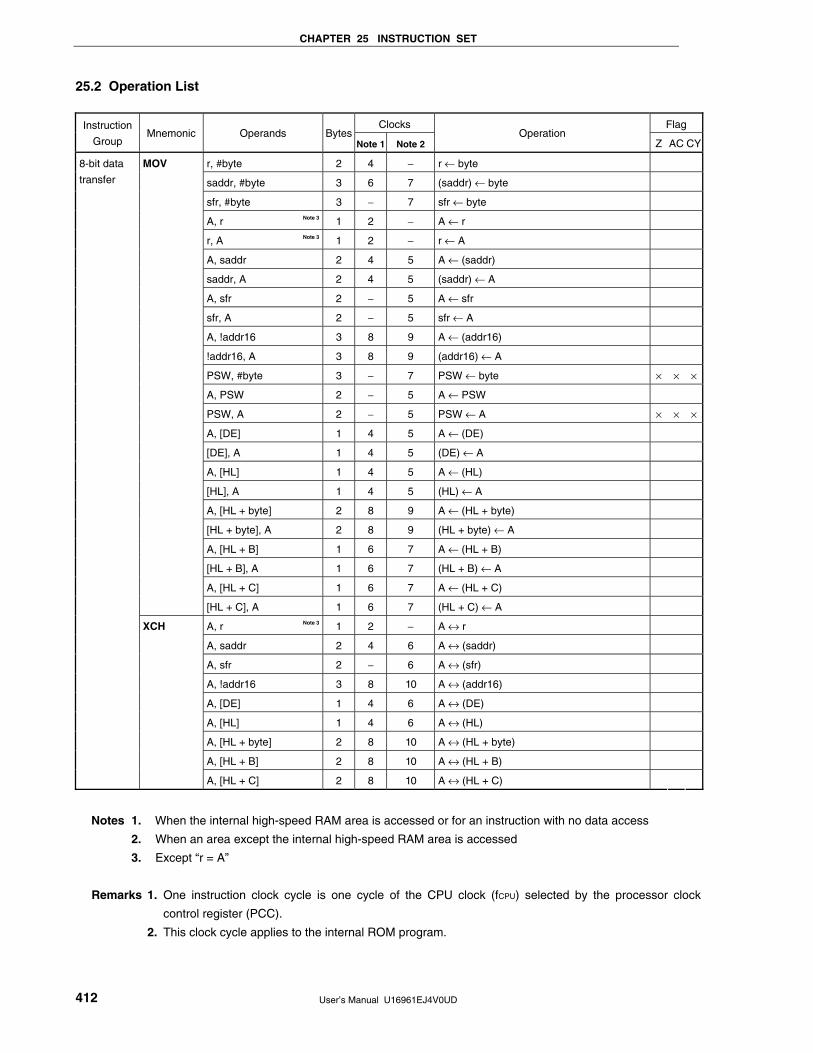
CHAPTER 25 INSTRUCTION SET
User’s Manual U16961EJ4V0UD 412
25.2 Operation List
Clocks Flag Instruction
Group Mnemonic Operands Bytes
Note 1 Note 2 Operation
Z AC CY
r, #byte 2 4 − r ← byte
saddr, #byte 3 6 7 (saddr) ← byte
sfr, #byte 3 − 7 sfr ← byte
A, r Note 3 1 2 − A ← r
r, A Note 3 1 2 − r ← A
A, saddr 2 4 5 A ← (saddr)
saddr, A 2 4 5 (saddr) ← A
A, sfr 2 − 5 A ← sfr
sfr, A 2 − 5 sfr ← A
A, !addr16 3 8 9 A ← (addr16)
!addr16, A 3 8 9 (addr16) ← A
PSW, #byte 3 − 7 PSW ← byte × × ×
A, PSW 2 − 5 A ← PSW
PSW, A 2 − 5 PSW ← A × × ×
A, [DE] 1 4 5 A ← (DE)
[DE], A 1 4 5 (DE) ← A
A, [HL] 1 4 5 A ← (HL)
[HL], A 1 4 5 (HL) ← A
A, [HL + byte] 2 8 9 A ← (HL + byte)
[HL + byte], A 2 8 9 (HL + byte) ← A
A, [HL + B] 1 6 7 A ← (HL + B)
[HL + B], A 1 6 7 (HL + B) ← A
A, [HL + C] 1 6 7 A ← (HL + C)
MOV
[HL + C], A 1 6 7 (HL + C) ← A
A, r Note 3 1 2 − A ↔ r
A, saddr 2 4 6 A ↔ (saddr)
A, sfr 2 − 6 A ↔ (sfr)
A, !addr16 3 8 10 A ↔ (addr16)
A, [DE] 1 4 6 A ↔ (DE)
A, [HL] 1 4 6 A ↔ (HL)
A, [HL + byte] 2 8 10 A ↔ (HL + byte)
A, [HL + B] 2 8 10 A ↔ (HL + B)
8-bit data
transfer
XCH
A, [HL + C] 2 8 10 A ↔ (HL + C)
Notes 1. When the internal high-speed RAM area is accessed or for an instruction with no data access
2. When an area except the internal high-speed RAM area is accessed
3. Except “r = A”
Remarks 1. One instruction clock cycle is one cycle of the CPU clock (fCPU) selected by the processor clock
control register (PCC).
2. This clock cycle applies to the internal ROM program.
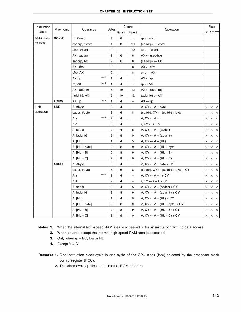
CHAPTER 25 INSTRUCTION SET
User’s Manual U16961EJ4V0UD 413
Clocks Flag Instruction
Group Mnemonic Operands Bytes
Note 1 Note 2 Operation
Z AC CY
rp, #word 3 6 − rp ← word
saddrp, #word 4 8 10 (saddrp) ← word
sfrp, #word 4 − 10 sfrp ← word
AX, saddrp 2 6 8 AX ← (saddrp)
saddrp, AX 2 6 8 (saddrp) ← AX
AX, sfrp 2 − 8 AX ← sfrp
sfrp, AX 2 − 8 sfrp ← AX
AX, rp Note 3 1 4 − AX ← rp
rp, AX Note 3 1 4 − rp ← AX
AX, !addr16 3 10 12 AX ← (addr16)
MOVW
!addr16, AX 3 10 12 (addr16) ← AX
16-bit data
transfer
XCHW AX, rp Note 3 1 4 − AX ↔ rp
A, #byte 2 4 − A, CY ← A + byte × × ×
saddr, #byte 3 6 8 (saddr), CY ← (saddr) + byte × × ×
A, r Note 4 2 4 − A, CY ← A + r × × ×
r, A 2 4 − r, CY ← r + A × × ×
A, saddr 2 4 5 A, CY ← A + (saddr) × × ×
A, !addr16 3 8 9 A, CY ← A + (addr16) × × ×
A, [HL] 1 4 5 A, CY ← A + (HL) × × ×
A, [HL + byte] 2 8 9 A, CY ← A + (HL + byte) × × ×
A, [HL + B] 2 8 9 A, CY ← A + (HL + B) × × ×
ADD
A, [HL + C] 2 8 9 A, CY ← A + (HL + C) × × ×
A, #byte 2 4 − A, CY ← A + byte + CY × × ×
saddr, #byte 3 6 8 (saddr), CY ← (saddr) + byte + CY × × ×
A, r Note 4 2 4 − A, CY ← A + r + CY × × ×
r, A 2 4 − r, CY ← r + A + CY × × ×
A, saddr 2 4 5 A, CY ← A + (saddr) + CY × × ×
A, !addr16 3 8 9 A, CY ← A + (addr16) + CY × × ×
A, [HL] 1 4 5 A, CY ← A + (HL) + CY × × ×
A, [HL + byte] 2 8 9 A, CY ← A + (HL + byte) + CY × × ×
A, [HL + B] 2 8 9 A, CY ← A + (HL + B) + CY × × ×
8-bit
operation
ADDC
A, [HL + C] 2 8 9 A, CY ← A + (HL + C) + CY × × ×
Notes 1. When the internal high-speed RAM area is accessed or for an instruction with no data access
2. When an area except the internal high-speed RAM area is accessed
3. Only when rp = BC, DE or HL
4. Except “r = A”
Remarks 1. One instruction clock cycle is one cycle of the CPU clock (fCPU) selected by the processor clock
control register (PCC).
2. This clock cycle applies to the internal ROM program.
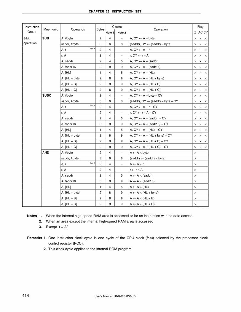
CHAPTER 25 INSTRUCTION SET
User’s Manual U16961EJ4V0UD 414
Clocks Flag Instruction
Group Mnemonic Operands Bytes
Note 1 Note 2 Operation
Z AC CY
A, #byte 2 4 − A, CY ← A − byte × × ×
saddr, #byte 3 6 8 (saddr), CY ← (saddr) − byte × × ×
A, r Note 3 2 4 − A, CY ← A − r × × ×
r, A 2 4 − r, CY ← r − A × × ×
A, saddr 2 4 5 A, CY ← A − (saddr) × × ×
A, !addr16 3 8 9 A, CY ← A − (addr16) × × ×
A, [HL] 1 4 5 A, CY ← A − (HL) × × ×
A, [HL + byte] 2 8 9 A, CY ← A − (HL + byte) × × ×
A, [HL + B] 2 8 9 A, CY ← A − (HL + B) × × ×
SUB
A, [HL + C] 2 8 9 A, CY ← A − (HL + C) × × ×
A, #byte 2 4 − A, CY ← A − byte − CY × × ×
saddr, #byte 3 6 8 (saddr), CY ← (saddr) − byte − CY × × ×
A, r Note 3 2 4 − A, CY ← A − r − CY × × ×
r, A 2 4 − r, CY ← r − A − CY × × ×
A, saddr 2 4 5 A, CY ← A − (saddr) − CY × × ×
A, !addr16 3 8 9 A, CY ← A − (addr16) − CY × × ×
A, [HL] 1 4 5 A, CY ← A − (HL) − CY × × ×
A, [HL + byte] 2 8 9 A, CY ← A − (HL + byte) − CY × × ×
A, [HL + B] 2 8 9 A, CY ← A − (HL + B) − CY × × ×
SUBC
A, [HL + C] 2 8 9 A, CY ← A − (HL + C) − CY × × ×
A, #byte 2 4 − A ← A ∧ byte ×
saddr, #byte 3 6 8 (saddr) ← (saddr) ∧ byte ×
A, r Note 3 2 4 − A ← A ∧ r ×
r, A 2 4 − r ← r ∧ A ×
A, saddr 2 4 5 A ← A ∧ (saddr) ×
A, !addr16 3 8 9 A ← A ∧ (addr16) ×
A, [HL] 1 4 5 A ← A ∧ (HL) ×
A, [HL + byte] 2 8 9 A ← A ∧ (HL + byte) ×
A, [HL + B] 2 8 9 A ← A ∧ (HL + B) ×
8-bit
operation
AND
A, [HL + C] 2 8 9 A ← A ∧ (HL + C) ×
Notes 1. When the internal high-speed RAM area is accessed or for an instruction with no data access
2. When an area except the internal high-speed RAM area is accessed
3. Except “r = A”
Remarks 1. One instruction clock cycle is one cycle of the CPU clock (fCPU) selected by the processor clock
control register (PCC).
2. This clock cycle applies to the internal ROM program.
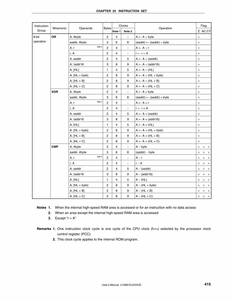
CHAPTER 25 INSTRUCTION SET
User’s Manual U16961EJ4V0UD 415
Clocks Flag Instruction
Group Mnemonic Operands Bytes
Note 1 Note 2 Operation
Z AC CY
A, #byte 2 4 − A ← A ∨ byte ×
saddr, #byte 3 6 8 (saddr) ← (saddr) ∨ byte ×
A, r Note 3 2 4 − A ← A ∨ r ×
r, A 2 4 − r ← r ∨ A ×
A, saddr 2 4 5 A ← A ∨ (saddr) ×
A, !addr16 3 8 9 A ← A ∨ (addr16) ×
A, [HL] 1 4 5 A ← A ∨ (HL) ×
A, [HL + byte] 2 8 9 A ← A ∨ (HL + byte) ×
A, [HL + B] 2 8 9 A ← A ∨ (HL + B) ×
OR
A, [HL + C] 2 8 9 A ← A ∨ (HL + C) ×
A, #byte 2 4 − A ← A ∨ byte ×
saddr, #byte 3 6 8 (saddr) ← (saddr) ∨ byte ×
A, r Note 3 2 4 − A ← A ∨ r ×
r, A 2 4 − r ← r ∨ A ×
A, saddr 2 4 5 A ← A ∨ (saddr) ×
A, !addr16 3 8 9 A ← A ∨ (addr16) ×
A, [HL] 1 4 5 A ← A ∨ (HL) ×
A, [HL + byte] 2 8 9 A ← A ∨ (HL + byte) ×
A, [HL + B] 2 8 9 A ← A ∨ (HL + B) ×
XOR
A, [HL + C] 2 8 9 A ← A ∨ (HL + C) ×
A, #byte 2 4 − A − byte × × ×
saddr, #byte 3 6 8 (saddr) − byte × × ×
A, r Note 3 2 4 − A − r × × ×
r, A 2 4 − r − A × × ×
A, saddr 2 4 5 A − (saddr) × × ×
A, !addr16 3 8 9 A − (addr16) × × ×
A, [HL] 1 4 5 A − (HL) × × ×
A, [HL + byte] 2 8 9 A − (HL + byte) × × ×
A, [HL + B] 2 8 9 A − (HL + B) × × ×
8-bit
operation
CMP
A, [HL + C] 2 8 9 A − (HL + C) × × ×
Notes 1. When the internal high-speed RAM area is accessed or for an instruction with no data access
2. When an area except the internal high-speed RAM area is accessed
3. Except “r = A”
Remarks 1. One instruction clock cycle is one cycle of the CPU clock (fCPU) selected by the processor clock
control register (PCC).
2. This clock cycle applies to the internal ROM program.
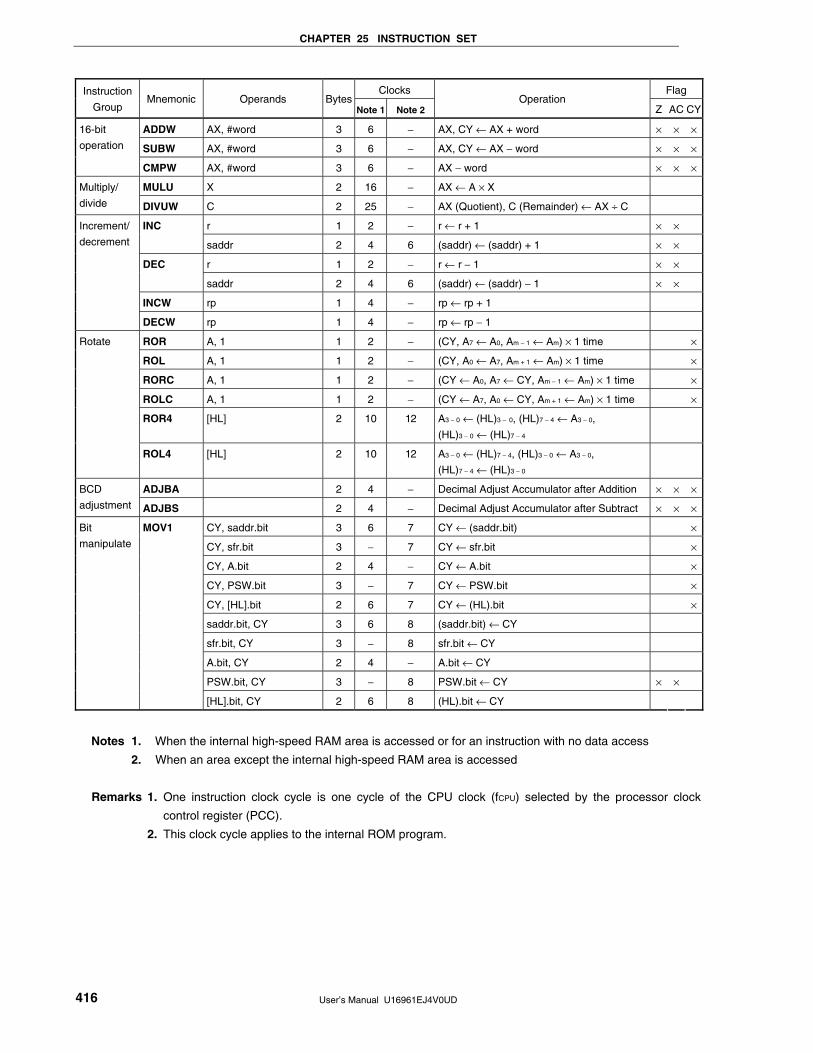
CHAPTER 25 INSTRUCTION SET
User’s Manual U16961EJ4V0UD 416
Clocks Flag Instruction
Group Mnemonic Operands Bytes
Note 1 Note 2 Operation
Z AC CY
ADDW AX, #word 3 6 − AX, CY ← AX + word × × ×
SUBW AX, #word 3 6 − AX, CY ← AX − word × × ×
16-bit
operation
CMPW AX, #word 3 6 − AX − word × × ×
MULU X 2 16 − AX ← A × X Multiply/
divide DIVUW C 2 25 − AX (Quotient), C (Remainder) ← AX ÷ C
r 1 2 − r ← r + 1 × × INC
saddr 2 4 6 (saddr) ← (saddr) + 1 × ×
r 1 2 − r ← r − 1 × × DEC
saddr 2 4 6 (saddr) ← (saddr) − 1 × ×
INCW rp 1 4 − rp ← rp + 1
Increment/
decrement
DECW rp 1 4 − rp ← rp − 1
ROR A, 1 1 2 − (CY, A7 ← A0, Am − 1 ← Am) × 1 time ×
ROL A, 1 1 2 − (CY, A0 ← A7, Am + 1 ← Am) × 1 time ×
RORC A, 1 1 2 − (CY ← A0, A7 ← CY, Am − 1 ← Am) × 1 time ×
ROLC A, 1 1 2 − (CY ← A7, A0 ← CY, Am + 1 ← Am) × 1 time ×
ROR4 [HL] 2 10 12 A3 − 0 ← (HL)3 − 0, (HL)7 − 4 ← A3 − 0,
(HL)3 − 0 ← (HL)7 − 4
Rotate
ROL4 [HL] 2 10 12 A3 − 0 ← (HL)7 − 4, (HL)3 − 0 ← A3 − 0,
(HL)7 − 4 ← (HL)3 − 0
ADJBA 2 4 − Decimal Adjust Accumulator after Addition × × ×BCD
adjustment ADJBS 2 4 − Decimal Adjust Accumulator after Subtract × × ×
CY, saddr.bit 3 6 7 CY ← (saddr.bit) ×
CY, sfr.bit 3 − 7 CY ← sfr.bit ×
CY, A.bit 2 4 − CY ← A.bit ×
CY, PSW.bit 3 − 7 CY ← PSW.bit ×
CY, [HL].bit 2 6 7 CY ← (HL).bit ×
saddr.bit, CY 3 6 8 (saddr.bit) ← CY
sfr.bit, CY 3 − 8 sfr.bit ← CY
A.bit, CY 2 4 − A.bit ← CY
PSW.bit, CY 3 − 8 PSW.bit ← CY × ×
Bit
manipulate
MOV1
[HL].bit, CY 2 6 8 (HL).bit ← CY
Notes 1. When the internal high-speed RAM area is accessed or for an instruction with no data access
2. When an area except the internal high-speed RAM area is accessed
Remarks 1. One instruction clock cycle is one cycle of the CPU clock (fCPU) selected by the processor clock
control register (PCC).
2. This clock cycle applies to the internal ROM program.
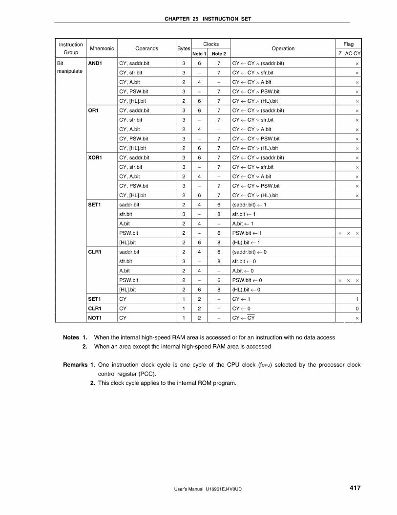
CHAPTER 25 INSTRUCTION SET
User’s Manual U16961EJ4V0UD 417
Clocks Flag Instruction
Group Mnemonic Operands Bytes
Note 1 Note 2 Operation
Z AC CY
CY, saddr.bit 3 6 7 CY ← CY ∧ (saddr.bit) ×
CY, sfr.bit 3 − 7 CY ← CY ∧ sfr.bit ×
CY, A.bit 2 4 − CY ← CY ∧ A.bit ×
CY, PSW.bit 3 − 7 CY ← CY ∧ PSW.bit ×
AND1
CY, [HL].bit 2 6 7 CY ← CY ∧ (HL).bit ×
CY, saddr.bit 3 6 7 CY ← CY ∨ (saddr.bit) ×
CY, sfr.bit 3 − 7 CY ← CY ∨ sfr.bit ×
CY, A.bit 2 4 − CY ← CY ∨ A.bit ×
CY, PSW.bit 3 − 7 CY ← CY ∨ PSW.bit ×
OR1
CY, [HL].bit 2 6 7 CY ← CY ∨ (HL).bit ×
CY, saddr.bit 3 6 7 CY ← CY ∨ (saddr.bit) ×
CY, sfr.bit 3 − 7 CY ← CY ∨ sfr.bit ×
CY, A.bit 2 4 − CY ← CY ∨ A.bit ×
CY, PSW.bit 3 − 7 CY ← CY ∨ PSW.bit ×
XOR1
CY, [HL].bit 2 6 7 CY ← CY ∨ (HL).bit ×
saddr.bit 2 4 6 (saddr.bit) ← 1
sfr.bit 3 − 8 sfr.bit ← 1
A.bit 2 4 − A.bit ← 1
PSW.bit 2 − 6 PSW.bit ← 1 × × ×
SET1
[HL].bit 2 6 8 (HL).bit ← 1
saddr.bit 2 4 6 (saddr.bit) ← 0
sfr.bit 3 − 8 sfr.bit ← 0
A.bit 2 4 − A.bit ← 0
PSW.bit 2 − 6 PSW.bit ← 0 × × ×
CLR1
[HL].bit 2 6 8 (HL).bit ← 0
SET1 CY 1 2 − CY ← 1 1
CLR1 CY 1 2 − CY ← 0 0
Bit
manipulate
NOT1 CY 1 2 − CY ← CY ×
Notes 1. When the internal high-speed RAM area is accessed or for an instruction with no data access
2. When an area except the internal high-speed RAM area is accessed
Remarks 1. One instruction clock cycle is one cycle of the CPU clock (fCPU) selected by the processor clock
control register (PCC).
2. This clock cycle applies to the internal ROM program.
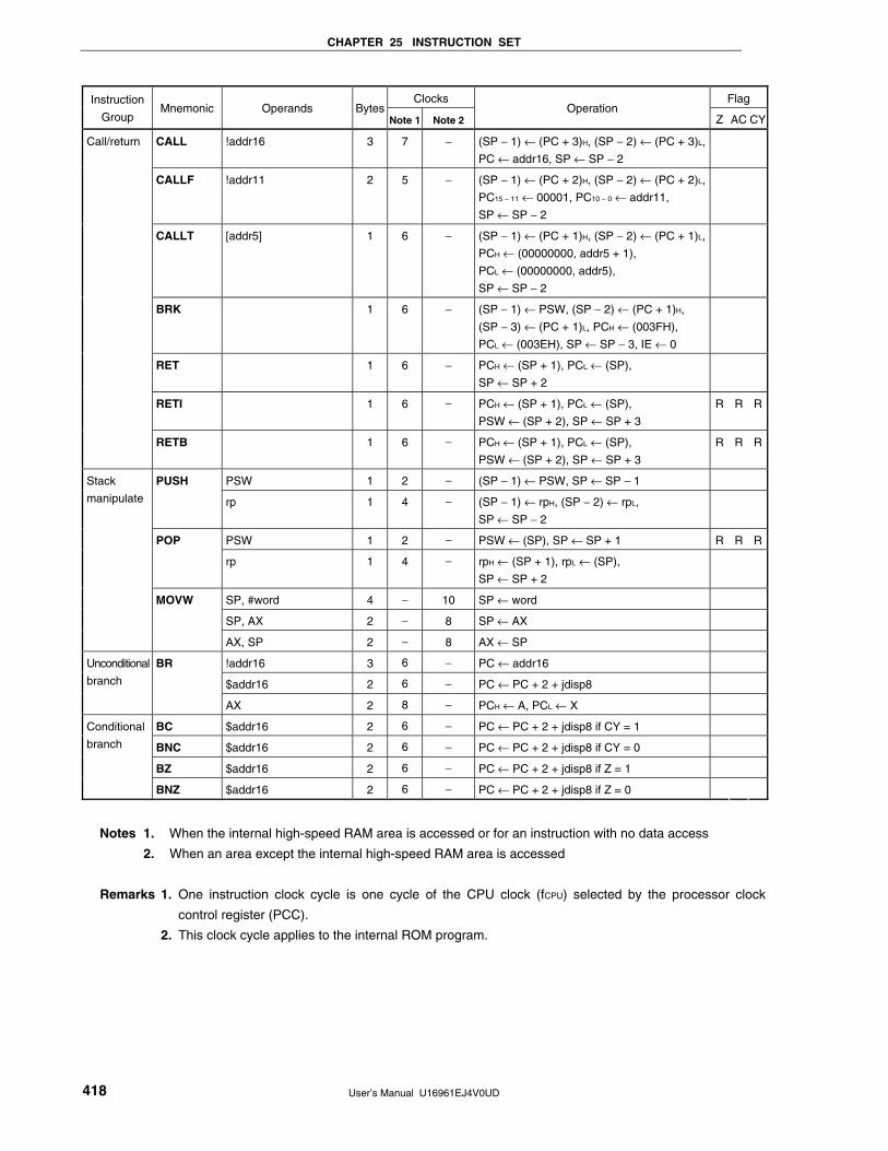
CHAPTER 25 INSTRUCTION SET
User’s Manual U16961EJ4V0UD 418
Clocks Flag Instruction
Group Mnemonic Operands Bytes
Note 1 Note 2 Operation
Z AC CY
CALL !addr16 3 7 − (SP − 1) ← (PC + 3)H, (SP − 2) ← (PC + 3)L,
PC ← addr16, SP ← SP − 2
CALLF !addr11 2 5 − (SP − 1) ← (PC + 2)H, (SP − 2) ← (PC + 2)L,
PC15 − 11 ← 00001, PC10 − 0 ← addr11,
SP ← SP − 2
CALLT [addr5] 1 6 − (SP − 1) ← (PC + 1)H, (SP − 2) ← (PC + 1)L,
PCH ← (00000000, addr5 + 1),
PCL ← (00000000, addr5),
SP ← SP − 2
BRK 1 6 − (SP − 1) ← PSW, (SP − 2) ← (PC + 1)H,
(SP − 3) ← (PC + 1)L, PCH ← (003FH),
PCL ← (003EH), SP ← SP − 3, IE ← 0
RET 1 6 − PCH ← (SP + 1), PCL ← (SP),
SP ← SP + 2
RETI 1 6 − PCH ← (SP + 1), PCL ← (SP),
PSW ← (SP + 2), SP ← SP + 3
R R R
Call/return
RETB 1 6 − PCH ← (SP + 1), PCL ← (SP),
PSW ← (SP + 2), SP ← SP + 3
R R R
PSW 1 2 − (SP − 1) ← PSW, SP ← SP − 1 PUSH
rp 1 4 − (SP − 1) ← rpH, (SP − 2) ← rpL,
SP ← SP − 2
PSW 1 2 − PSW ← (SP), SP ← SP + 1 R R RPOP
rp 1 4 − rpH ← (SP + 1), rpL ← (SP),
SP ← SP + 2
SP, #word 4 − 10 SP ← word
SP, AX 2 − 8 SP ← AX
Stack
manipulate
MOVW
AX, SP 2 − 8 AX ← SP
!addr16 3 6 − PC ← addr16
$addr16 2 6 − PC ← PC + 2 + jdisp8
Unconditional
branch
BR
AX 2 8 − PCH ← A, PCL ← X
BC $addr16 2 6 − PC ← PC + 2 + jdisp8 if CY = 1
BNC $addr16 2 6 − PC ← PC + 2 + jdisp8 if CY = 0
BZ $addr16 2 6 − PC ← PC + 2 + jdisp8 if Z = 1
Conditional
branch
BNZ $addr16 2 6 − PC ← PC + 2 + jdisp8 if Z = 0
Notes 1. When the internal high-speed RAM area is accessed or for an instruction with no data access
2. When an area except the internal high-speed RAM area is accessed
Remarks 1. One instruction clock cycle is one cycle of the CPU clock (fCPU) selected by the processor clock
control register (PCC).
2. This clock cycle applies to the internal ROM program.

CHAPTER 25 INSTRUCTION SET
User’s Manual U16961EJ4V0UD 419
Clocks Flag Instruction
Group Mnemonic Operands Bytes
Note 1 Note 2 Operation
Z AC CY
saddr.bit, $addr16 3 8 9 PC ← PC + 3 + jdisp8 if (saddr.bit) = 1
sfr.bit, $addr16 4 − 11 PC ← PC + 4 + jdisp8 if sfr.bit = 1
A.bit, $addr16 3 8 − PC ← PC + 3 + jdisp8 if A.bit = 1
PSW.bit, $addr16 3 − 9 PC ← PC + 3 + jdisp8 if PSW.bit = 1
BT
[HL].bit, $addr16 3 10 11 PC ← PC + 3 + jdisp8 if (HL).bit = 1
saddr.bit, $addr16 4 10 11 PC ← PC + 4 + jdisp8 if (saddr.bit) = 0
sfr.bit, $addr16 4 − 11 PC ← PC + 4 + jdisp8 if sfr.bit = 0
A.bit, $addr16 3 8 − PC ← PC + 3 + jdisp8 if A.bit = 0
PSW.bit, $addr16 4 − 11 PC ← PC + 4 + jdisp8 if PSW.bit = 0
BF
[HL].bit, $addr16 3 10 11 PC ← PC + 3 + jdisp8 if (HL).bit = 0
saddr.bit, $addr16 4 10 12 PC ← PC + 4 + jdisp8 if (saddr.bit) = 1
then reset (saddr.bit)
sfr.bit, $addr16 4 − 12 PC ← PC + 4 + jdisp8 if sfr.bit = 1
then reset sfr.bit
A.bit, $addr16 3 8 − PC ← PC + 3 + jdisp8 if A.bit = 1
then reset A.bit
PSW.bit, $addr16 4 − 12 PC ← PC + 4 + jdisp8 if PSW.bit = 1
then reset PSW.bit
× × ×
BTCLR
[HL].bit, $addr16 3 10 12 PC ← PC + 3 + jdisp8 if (HL).bit = 1
then reset (HL).bit
B, $addr16 2 6 − B ← B − 1, then
PC ← PC + 2 + jdisp8 if B ≠ 0
C, $addr16 2 6 − C ← C −1, then
PC ← PC + 2 + jdisp8 if C ≠ 0
Conditional
branch
DBNZ
saddr, $addr16 3 8 10 (saddr) ← (saddr) − 1, then
PC ← PC + 3 + jdisp8 if (saddr) ≠ 0
SEL RBn 2 4 − RBS1, 0 ← n
NOP 1 2 − No Operation
EI 2 − 6 IE ← 1 (Enable Interrupt)
DI 2 − 6 IE ← 0 (Disable Interrupt)
HALT 2 6 − Set HALT Mode
CPU
control
STOP 2 6 − Set STOP Mode
Notes 1. When the internal high-speed RAM area is accessed or for an instruction with no data access
2. When an area except the internal high-speed RAM area is accessed
Remarks 1. One instruction clock cycle is one cycle of the CPU clock (fCPU) selected by the processor clock
control register (PCC).
2. This clock cycle applies to the internal ROM program.
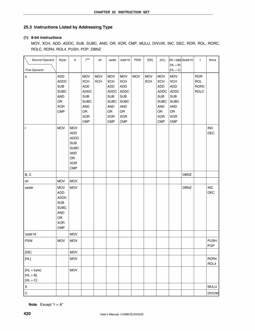
CHAPTER 25 INSTRUCTION SET
User’s Manual U16961EJ4V0UD 420
25.3 Instructions Listed by Addressing Type
(1) 8-bit instructions
MOV, XCH, ADD, ADDC, SUB, SUBC, AND, OR, XOR, CMP, MULU, DIVUW, INC, DEC, ROR, ROL, RORC,
ROLC, ROR4, ROL4, PUSH, POP, DBNZ
Second Operand
First Operand
#byte A rNote sfr saddr !addr16 PSW [DE] [HL] [HL + byte]
[HL + B]
[HL + C]
$addr16 1 None
A ADD
ADDC
SUB
SUBC
AND
OR
XOR
CMP
MOV
XCH
ADD
ADDC
SUB
SUBC
AND
OR
XOR
CMP
MOV
XCH
MOV
XCH
ADD
ADDC
SUB
SUBC
AND
OR
XOR
CMP
MOV
XCH
ADD
ADDC
SUB
SUBC
AND
OR
XOR
CMP
MOV MOV
XCH
MOV
XCH
ADD
ADDC
SUB
SUBC
AND
OR
XOR
CMP
MOV
XCH
ADD
ADDC
SUB
SUBC
AND
OR
XOR
CMP
ROR
ROL
RORC
ROLC
r MOV MOV
ADD
ADDC
SUB
SUBC
AND
OR
XOR
CMP
INC
DEC
B, C DBNZ
sfr MOV MOV
saddr MOV
ADD
ADDC
SUB
SUBC
AND
OR
XOR
CMP
MOV DBNZ INC
DEC
!addr16 MOV
PSW MOV MOV PUSH
POP
[DE] MOV
[HL] MOV ROR4
ROL4
[HL + byte]
[HL + B]
[HL + C]
MOV
X MULU
C DIVUW
Note Except “r = A”
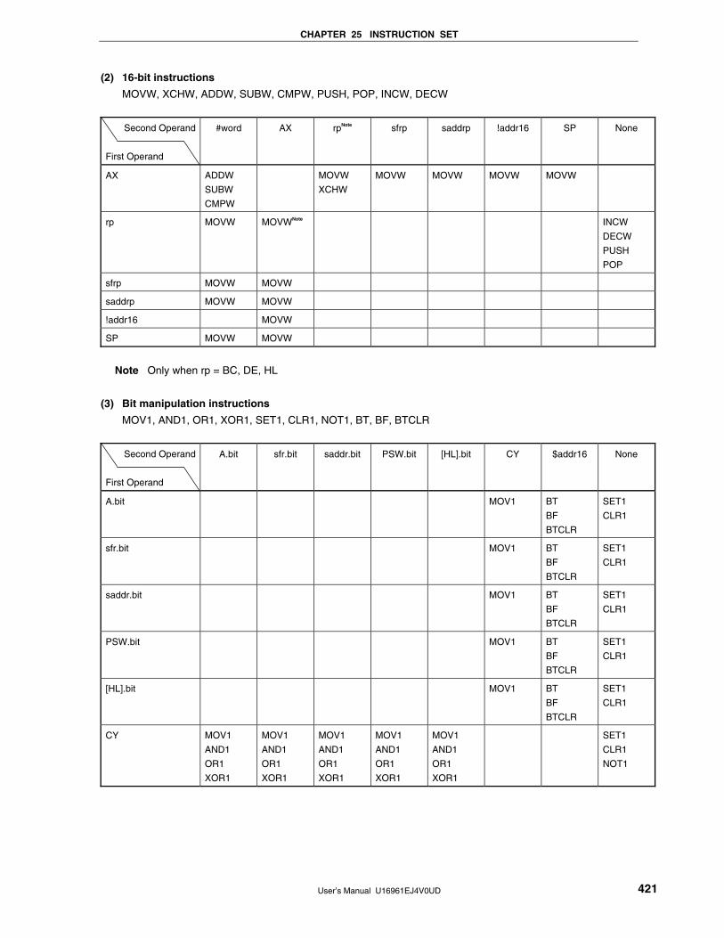
CHAPTER 25 INSTRUCTION SET
User’s Manual U16961EJ4V0UD 421
(2) 16-bit instructions
MOVW, XCHW, ADDW, SUBW, CMPW, PUSH, POP, INCW, DECW
Second Operand
First Operand
#word AX rpNote sfrp saddrp !addr16 SP None
AX ADDW
SUBW
CMPW
MOVW
XCHW
MOVW MOVW MOVW MOVW
rp MOVW MOVWNote INCW
DECW
PUSH
POP
sfrp MOVW MOVW
saddrp MOVW MOVW
!addr16 MOVW
SP MOVW MOVW
Note Only when rp = BC, DE, HL
(3) Bit manipulation instructions
MOV1, AND1, OR1, XOR1, SET1, CLR1, NOT1, BT, BF, BTCLR
Second Operand
First Operand
A.bit sfr.bit saddr.bit PSW.bit [HL].bit CY $addr16 None
A.bit MOV1 BT
BF
BTCLR
SET1
CLR1
sfr.bit MOV1 BT
BF
BTCLR
SET1
CLR1
saddr.bit MOV1 BT
BF
BTCLR
SET1
CLR1
PSW.bit MOV1 BT
BF
BTCLR
SET1
CLR1
[HL].bit MOV1 BT
BF
BTCLR
SET1
CLR1
CY MOV1
AND1
OR1
XOR1
MOV1
AND1
OR1
XOR1
MOV1
AND1
OR1
XOR1
MOV1
AND1
OR1
XOR1
MOV1
AND1
OR1
XOR1
SET1
CLR1
NOT1
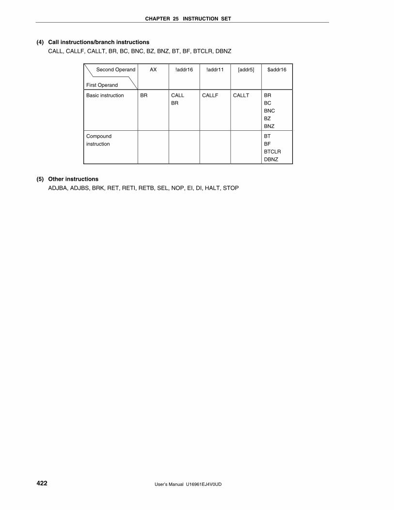
CHAPTER 25 INSTRUCTION SET
User’s Manual U16961EJ4V0UD 422
(4) Call instructions/branch instructions
CALL, CALLF, CALLT, BR, BC, BNC, BZ, BNZ, BT, BF, BTCLR, DBNZ
Second Operand
First Operand
AX !addr16 !addr11 [addr5] $addr16
Basic instruction BR CALL
BR
CALLF CALLT BR
BC
BNC
BZ
BNZ
Compound
instruction
BT
BF
BTCLR
DBNZ
(5) Other instructions
ADJBA, ADJBS, BRK, RET, RETI, RETB, SEL, NOP, EI, DI, HALT, STOP
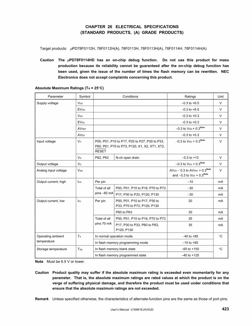
User’s Manual U16961EJ4V0UD 423
CHAPTER 26 ELECTRICAL SPECIFICATIONS (STANDARD PRODUCTS, (A) GRADE PRODUCTS)
Target products: μPD78F0112H, 78F0112H(A), 78F0113H, 78F0113H(A), 78F0114H, 78F0114H(A) Caution The μPD78F0114HD has an on-chip debug function. Do not use this product for mass
production because its reliability cannot be guaranteed after the on-chip debug function has been used, given the issue of the number of times the flash memory can be rewritten. NEC Electronics does not accept complaints concerning this product.
Absolute Maximum Ratings (TA = 25°C)
Parameter Symbol Conditions Ratings Unit
VDD −0.3 to +6.5 V
EVDD −0.3 to +6.5 V
VSS −0.3 to +0.3 V
EVSS −0.3 to +0.3 V
AVREF −0.3 to VDD + 0.3Note V
Supply voltage
AVSS −0.3 to +0.3 V
VI1 P00, P01, P10 to P17, P20 to P27, P30 to P33, P60, P61, P70 to P73, P120, X1, X2, XT1, XT2, RESET
−0.3 to VDD + 0.3Note V Input voltage
VI2 P62, P63 N-ch open drain −0.3 to +13 V
Output voltage VO −0.3 to VDD + 0.3Note V
Analog input voltage VAN AVSS − 0.3 to AVREF + 0.3Note
and −0.3 to VDD + 0.3Note V
Per pin −10 mA
P00, P01, P10 to P16, P70 to P73 −30 mA
Output current, high IOH
Total of all pins −60 mA P17, P30 to P33, P120, P130 −30 mA
P00, P01, P10 to P17, P30 to P33, P70 to P73, P120, P130
20 mA Per pin
P60 to P63 30 mA
P00, P01, P10 to P16, P70 to P73 35 mA
Output current, low IOL
Total of all pins 70 mA P17, P30 to P33, P60 to P63,
P120, P130 35 mA
In normal operation mode −40 to +85 Operating ambient temperature
TA
In flash memory programming mode −10 to +65
°C
In flash memory blank state −65 to +150 Storage temperature Tstg
In flash memory programmed state −40 to +125
°C
Note Must be 6.5 V or lower. Caution Product quality may suffer if the absolute maximum rating is exceeded even momentarily for any
parameter. That is, the absolute maximum ratings are rated values at which the product is on the verge of suffering physical damage, and therefore the product must be used under conditions that ensure that the absolute maximum ratings are not exceeded.
Remark Unless specified otherwise, the characteristics of alternate-function pins are the same as those of port pins.
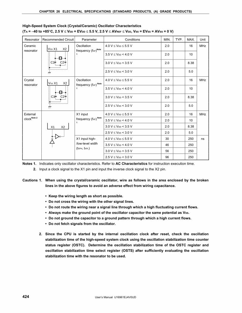
CHAPTER 26 ELECTRICAL SPECIFICATIONS (STANDARD PRODUCTS, (A) GRADE PRODUCTS)
User’s Manual U16961EJ4V0UD 424
High-Speed System Clock (Crystal/Ceramic) Oscillator Characteristics (TA = −40 to +85°C, 2.5 V ≤ VDD = EVDD ≤ 5.5 V, 2.5 V ≤ AVREF ≤ VDD, VSS = EVSS = AVSS = 0 V)
Resonator Recommended Circuit Parameter Conditions MIN. TYP. MAX. Unit
4.0 V ≤ VDD ≤ 5.5 V 2.0 16
3.5 V ≤ VDD < 4.0 V 2.0 10
3.0 V ≤ VDD < 3.5 V 2.0 8.38
Ceramic resonator
C1
X2X1VSS
C2
Oscillation frequency (fXP)Note
1
2.5 V ≤ VDD < 3.0 V 2.0 5.0
MHz
4.0 V ≤ VDD ≤ 5.5 V 2.0 16
3.5 V ≤ VDD < 4.0 V 2.0 10
3.0 V ≤ VDD < 3.5 V 2.0 8.38
Crystal resonator
C1
X2X1VSS
C2
Oscillation frequency (fXP) Note
1
2.5 V ≤ VDD < 3.0 V 2.0 5.0
MHz
4.0 V ≤ VDD ≤ 5.5 V 2.0 16
3.5 V ≤ VDD < 4.0 V 2.0 10
3.0 V ≤ VDD < 3.5 V 2.0 8.38
X1 input frequency (fXP) Note
1
2.5 V ≤ VDD < 3.0 V 2.0 5.0
MHz
4.0 V ≤ VDD ≤ 5.5 V 30 250
3.5 V ≤ VDD < 4.0 V 46 250
3.0 V ≤ VDD < 3.5 V 56 250
External clockNote 2
X2X1
X1 input high-/low-level width (tXPH, tXPL)
2.5 V ≤ VDD < 3.0 V 96 250
ns
Notes 1. Indicates only oscillator characteristics. Refer to AC Characteristics for instruction execution time. 2. Input a clock signal to the X1 pin and input the inverse clock signal to the X2 pin.
Cautions 1. When using the crystal/ceramic oscillator, wire as follows in the area enclosed by the broken
lines in the above figures to avoid an adverse effect from wiring capacitance. • Keep the wiring length as short as possible. • Do not cross the wiring with the other signal lines. • Do not route the wiring near a signal line through which a high fluctuating current flows. • Always make the ground point of the oscillator capacitor the same potential as VSS. • Do not ground the capacitor to a ground pattern through which a high current flows. • Do not fetch signals from the oscillator. 2. Since the CPU is started by the internal oscillation clock after reset, check the oscillation
stabilization time of the high-speed system clock using the oscillation stabilization time counter status register (OSTC). Determine the oscillation stabilization time of the OSTC register and oscillation stabilization time select register (OSTS) after sufficiently evaluating the oscillation stabilization time with the resonator to be used.
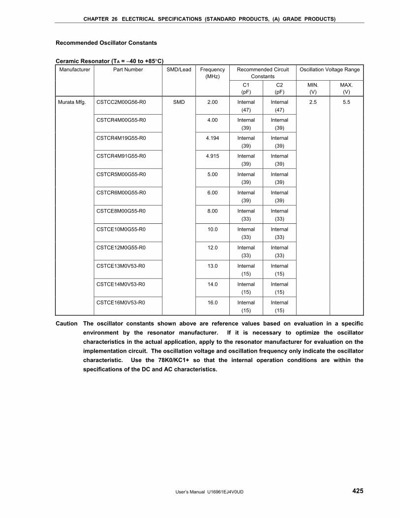
CHAPTER 26 ELECTRICAL SPECIFICATIONS (STANDARD PRODUCTS, (A) GRADE PRODUCTS)
User’s Manual U16961EJ4V0UD 425
Recommended Oscillator Constants Ceramic Resonator (TA = −40 to +85°C)
Recommended Circuit Constants
Oscillation Voltage Range Manufacturer Part Number SMD/Lead Frequency (MHz)
C1 (pF)
C2 (pF)
MIN. (V)
MAX. (V)
CSTCC2M00G56-R0 2.00 Internal (47)
Internal (47)
CSTCR4M00G55-R0 4.00 Internal (39)
Internal (39)
CSTCR4M19G55-R0 4.194 Internal (39)
Internal (39)
CSTCR4M91G55-R0 4.915 Internal (39)
Internal (39)
CSTCR5M00G55-R0 5.00 Internal (39)
Internal (39)
CSTCR6M00G55-R0 6.00 Internal (39)
Internal (39)
CSTCE8M00G55-R0 8.00 Internal (33)
Internal (33)
CSTCE10M0G55-R0 10.0 Internal (33)
Internal (33)
CSTCE12M0G55-R0 12.0 Internal (33)
Internal (33)
CSTCE13M0V53-R0 13.0 Internal (15)
Internal (15)
CSTCE14M0V53-R0 14.0 Internal (15)
Internal (15)
Murata Mfg.
CSTCE16M0V53-R0
SMD
16.0 Internal (15)
Internal (15)
2.5 5.5
Caution The oscillator constants shown above are reference values based on evaluation in a specific environment by the resonator manufacturer. If it is necessary to optimize the oscillator characteristics in the actual application, apply to the resonator manufacturer for evaluation on the implementation circuit. The oscillation voltage and oscillation frequency only indicate the oscillator characteristic. Use the 78K0/KC1+ so that the internal operation conditions are within the specifications of the DC and AC characteristics.
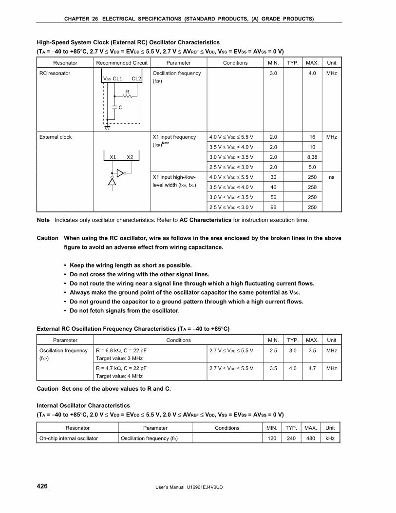
CHAPTER 26 ELECTRICAL SPECIFICATIONS (STANDARD PRODUCTS, (A) GRADE PRODUCTS)
User’s Manual U16961EJ4V0UD 426
High-Speed System Clock (External RC) Oscillator Characteristics (TA = −40 to +85°C, 2.7 V ≤ VDD = EVDD ≤ 5.5 V, 2.7 V ≤ AVREF ≤ VDD, VSS = EVSS = AVSS = 0 V)
Resonator Recommended Circuit Parameter Conditions MIN. TYP. MAX. Unit
RC resonator VSS CL1 CL2
R
C
Oscillation frequency (fXP)
3.0 4.0 MHz
4.0 V ≤ VDD ≤ 5.5 V 2.0 16
3.5 V ≤ VDD < 4.0 V 2.0 10
3.0 V ≤ VDD < 3.5 V 2.0 8.38
X1 input frequency (fXP)Note
2.5 V ≤ VDD < 3.0 V 2.0 5.0
MHz
4.0 V ≤ VDD ≤ 5.5 V 30 250
3.5 V ≤ VDD < 4.0 V 46 250
3.0 V ≤ VDD < 3.5 V 56 250
External clock
X2X1
X1 input high-/low-level width (tXH, tXL)
2.5 V ≤ VDD < 3.0 V 96 250
ns
Note Indicates only oscillator characteristics. Refer to AC Characteristics for instruction execution time. Caution When using the RC oscillator, wire as follows in the area enclosed by the broken lines in the above
figure to avoid an adverse effect from wiring capacitance. • Keep the wiring length as short as possible. • Do not cross the wiring with the other signal lines. • Do not route the wiring near a signal line through which a high fluctuating current flows. • Always make the ground point of the oscillator capacitor the same potential as VSS. • Do not ground the capacitor to a ground pattern through which a high current flows. • Do not fetch signals from the oscillator. External RC Oscillation Frequency Characteristics (TA = −40 to +85°C)
Parameter Conditions MIN. TYP. MAX. Unit
R = 6.8 kΩ, C = 22 pF Target value: 3 MHz
2.7 V ≤ VDD ≤ 5.5 V 2.5 3.0 3.5 MHz Oscillation frequency (fXP)
R = 4.7 kΩ, C = 22 pF Target value: 4 MHz
2.7 V ≤ VDD ≤ 5.5 V 3.5 4.0 4.7 MHz
Caution Set one of the above values to R and C. Internal Oscillator Characteristics (TA = −40 to +85°C, 2.0 V ≤ VDD = EVDD ≤ 5.5 V, 2.0 V ≤ AVREF ≤ VDD, VSS = EVSS = AVSS = 0 V)
Resonator Parameter Conditions MIN. TYP. MAX. Unit
On-chip internal oscillator Oscillation frequency (fR) 120 240 480 kHz
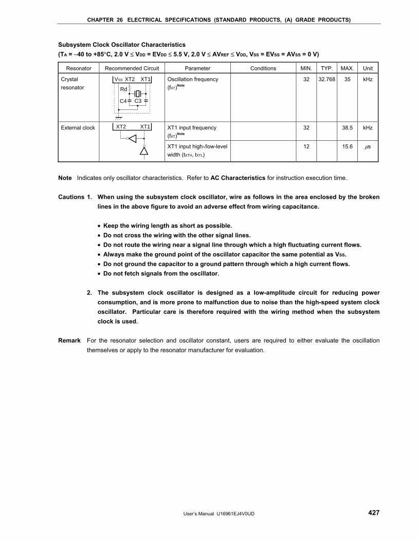
CHAPTER 26 ELECTRICAL SPECIFICATIONS (STANDARD PRODUCTS, (A) GRADE PRODUCTS)
User’s Manual U16961EJ4V0UD 427
Subsystem Clock Oscillator Characteristics (TA = −40 to +85°C, 2.0 V ≤ VDD = EVDD ≤ 5.5 V, 2.0 V ≤ AVREF ≤ VDD, VSS = EVSS = AVSS = 0 V)
Resonator Recommended Circuit Parameter Conditions MIN. TYP. MAX. Unit
Crystal resonator
XT1VSS XT2
C4 C3
Rd
Oscillation frequency (fXT)Note
32 32.768 35 kHz
XT1 input frequency (fXT)Note
32 38.5 kHz External clock XT1XT2
XT1 input high-/low-level width (tXTH, tXTL)
12 15.6 μs
Note Indicates only oscillator characteristics. Refer to AC Characteristics for instruction execution time. Cautions 1. When using the subsystem clock oscillator, wire as follows in the area enclosed by the broken
lines in the above figure to avoid an adverse effect from wiring capacitance. • Keep the wiring length as short as possible. • Do not cross the wiring with the other signal lines. • Do not route the wiring near a signal line through which a high fluctuating current flows. • Always make the ground point of the oscillator capacitor the same potential as VSS. • Do not ground the capacitor to a ground pattern through which a high current flows. • Do not fetch signals from the oscillator. 2. The subsystem clock oscillator is designed as a low-amplitude circuit for reducing power
consumption, and is more prone to malfunction due to noise than the high-speed system clock oscillator. Particular care is therefore required with the wiring method when the subsystem clock is used.
Remark For the resonator selection and oscillator constant, users are required to either evaluate the oscillation
themselves or apply to the resonator manufacturer for evaluation.
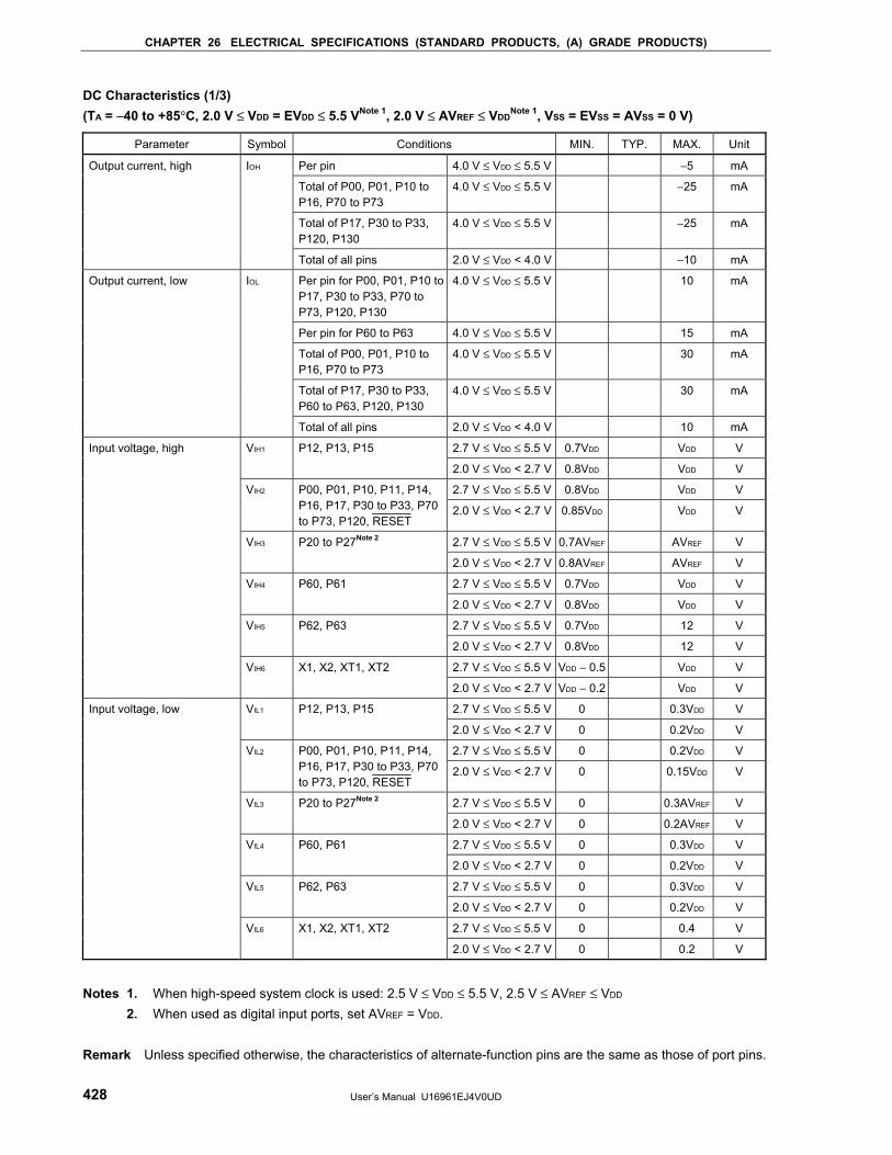
CHAPTER 26 ELECTRICAL SPECIFICATIONS (STANDARD PRODUCTS, (A) GRADE PRODUCTS)
User’s Manual U16961EJ4V0UD 428
DC Characteristics (1/3) (TA = −40 to +85°C, 2.0 V ≤ VDD = EVDD ≤ 5.5 VNote 1, 2.0 V ≤ AVREF ≤ VDD
Note 1, VSS = EVSS = AVSS = 0 V)
Parameter Symbol Conditions MIN. TYP. MAX. Unit
Per pin 4.0 V ≤ VDD ≤ 5.5 V −5 mA
Total of P00, P01, P10 to P16, P70 to P73
4.0 V ≤ VDD ≤ 5.5 V −25 mA
Total of P17, P30 to P33, P120, P130
4.0 V ≤ VDD ≤ 5.5 V −25 mA
Output current, high IOH
Total of all pins 2.0 V ≤ VDD < 4.0 V −10 mA
Per pin for P00, P01, P10 to P17, P30 to P33, P70 to P73, P120, P130
4.0 V ≤ VDD ≤ 5.5 V 10 mA
Per pin for P60 to P63 4.0 V ≤ VDD ≤ 5.5 V 15 mA
Total of P00, P01, P10 to P16, P70 to P73
4.0 V ≤ VDD ≤ 5.5 V 30 mA
Total of P17, P30 to P33, P60 to P63, P120, P130
4.0 V ≤ VDD ≤ 5.5 V 30 mA
Output current, low IOL
Total of all pins 2.0 V ≤ VDD < 4.0 V 10 mA
2.7 V ≤ VDD ≤ 5.5 V 0.7VDD VDD V VIH1 P12, P13, P15
2.0 V ≤ VDD < 2.7 V 0.8VDD VDD V
2.7 V ≤ VDD ≤ 5.5 V 0.8VDD VDD V VIH2 P00, P01, P10, P11, P14, P16, P17, P30 to P33, P70 to P73, P120, RESET
2.0 V ≤ VDD < 2.7 V 0.85VDD VDD V
2.7 V ≤ VDD ≤ 5.5 V 0.7AVREF AVREF V VIH3 P20 to P27Note 2
2.0 V ≤ VDD < 2.7 V 0.8AVREF AVREF V
2.7 V ≤ VDD ≤ 5.5 V 0.7VDD VDD V VIH4 P60, P61
2.0 V ≤ VDD < 2.7 V 0.8VDD VDD V
2.7 V ≤ VDD ≤ 5.5 V 0.7VDD 12 V VIH5 P62, P63
2.0 V ≤ VDD < 2.7 V 0.8VDD 12 V
2.7 V ≤ VDD ≤ 5.5 V VDD − 0.5 VDD V
Input voltage, high
VIH6 X1, X2, XT1, XT2
2.0 V ≤ VDD < 2.7 V VDD − 0.2 VDD V
2.7 V ≤ VDD ≤ 5.5 V 0 0.3VDD V VIL1 P12, P13, P15
2.0 V ≤ VDD < 2.7 V 0 0.2VDD V
2.7 V ≤ VDD ≤ 5.5 V 0 0.2VDD V VIL2 P00, P01, P10, P11, P14, P16, P17, P30 to P33, P70 to P73, P120, RESET
2.0 V ≤ VDD < 2.7 V 0 0.15VDD V
2.7 V ≤ VDD ≤ 5.5 V 0 0.3AVREF V VIL3 P20 to P27Note 2
2.0 V ≤ VDD < 2.7 V 0 0.2AVREF V
2.7 V ≤ VDD ≤ 5.5 V 0 0.3VDD V VIL4 P60, P61
2.0 V ≤ VDD < 2.7 V 0 0.2VDD V
2.7 V ≤ VDD ≤ 5.5 V 0 0.3VDD V VIL5 P62, P63
2.0 V ≤ VDD < 2.7 V 0 0.2VDD V
2.7 V ≤ VDD ≤ 5.5 V 0 0.4 V
Input voltage, low
VIL6 X1, X2, XT1, XT2
2.0 V ≤ VDD < 2.7 V 0 0.2 V
Notes 1. When high-speed system clock is used: 2.5 V ≤ VDD ≤ 5.5 V, 2.5 V ≤ AVREF ≤ VDD 2. When used as digital input ports, set AVREF = VDD. Remark Unless specified otherwise, the characteristics of alternate-function pins are the same as those of port pins.
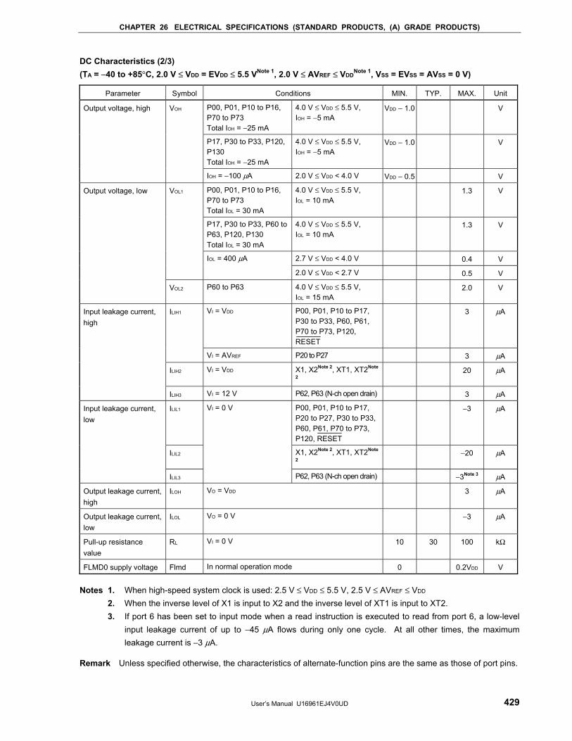
CHAPTER 26 ELECTRICAL SPECIFICATIONS (STANDARD PRODUCTS, (A) GRADE PRODUCTS)
User’s Manual U16961EJ4V0UD 429
DC Characteristics (2/3) (TA = −40 to +85°C, 2.0 V ≤ VDD = EVDD ≤ 5.5 VNote 1, 2.0 V ≤ AVREF ≤ VDD
Note 1, VSS = EVSS = AVSS = 0 V)
Parameter Symbol Conditions MIN. TYP. MAX. Unit
P00, P01, P10 to P16, P70 to P73 Total IOH = −25 mA
4.0 V ≤ VDD ≤ 5.5 V, IOH = −5 mA
VDD − 1.0 V
P17, P30 to P33, P120, P130 Total IOH = −25 mA
4.0 V ≤ VDD ≤ 5.5 V, IOH = −5 mA
VDD − 1.0 V
Output voltage, high VOH
IOH = −100 μA 2.0 V ≤ VDD < 4.0 V VDD − 0.5 V
P00, P01, P10 to P16, P70 to P73 Total IOL = 30 mA
4.0 V ≤ VDD ≤ 5.5 V, IOL = 10 mA
1.3 V
P17, P30 to P33, P60 to P63, P120, P130 Total IOL = 30 mA
4.0 V ≤ VDD ≤ 5.5 V, IOL = 10 mA
1.3 V
2.7 V ≤ VDD < 4.0 V 0.4 V
VOL1
IOL = 400 μA
2.0 V ≤ VDD < 2.7 V 0.5 V
Output voltage, low
VOL2 P60 to P63 4.0 V ≤ VDD ≤ 5.5 V, IOL = 15 mA
2.0 V
VI = VDD P00, P01, P10 to P17, P30 to P33, P60, P61, P70 to P73, P120, RESET
3 μA ILIH1
VI = AVREF P20 to P27 3 μA
ILIH2 VI = VDD X1, X2Note 2, XT1, XT2Note
2 20 μA
Input leakage current, high
ILIH3 VI = 12 V P62, P63 (N-ch open drain) 3 μA
ILIL1 P00, P01, P10 to P17, P20 to P27, P30 to P33, P60, P61, P70 to P73, P120, RESET
−3 μA
ILIL2 X1, X2Note 2, XT1, XT2Note
2 −20 μA
Input leakage current, low
ILIL3
VI = 0 V
P62, P63 (N-ch open drain) −3Note 3 μA
Output leakage current, high
ILOH VO = VDD 3 μA
Output leakage current, low
ILOL VO = 0 V −3 μA
Pull-up resistance value
RL VI = 0 V 10 30 100 kΩ
FLMD0 supply voltage Flmd In normal operation mode 0 0.2VDD V Notes 1. When high-speed system clock is used: 2.5 V ≤ VDD ≤ 5.5 V, 2.5 V ≤ AVREF ≤ VDD 2. When the inverse level of X1 is input to X2 and the inverse level of XT1 is input to XT2. 3. If port 6 has been set to input mode when a read instruction is executed to read from port 6, a low-level
input leakage current of up to −45 μA flows during only one cycle. At all other times, the maximum leakage current is −3 μA.
Remark Unless specified otherwise, the characteristics of alternate-function pins are the same as those of port pins.
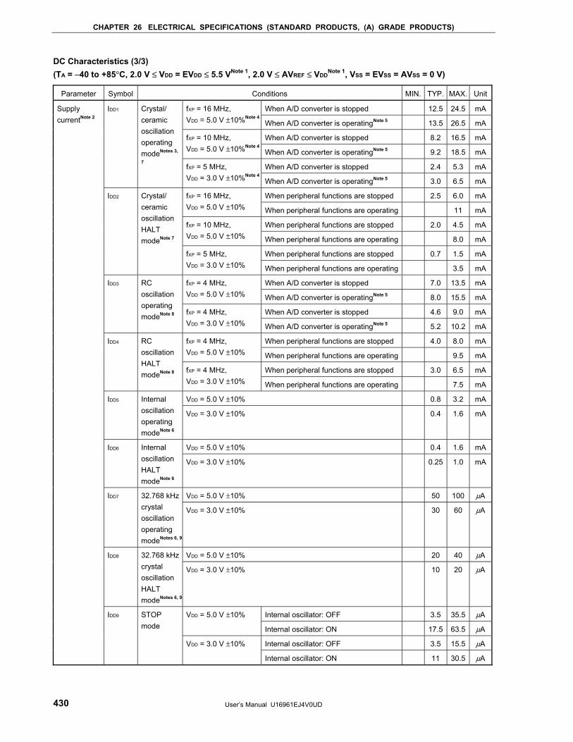
CHAPTER 26 ELECTRICAL SPECIFICATIONS (STANDARD PRODUCTS, (A) GRADE PRODUCTS)
User’s Manual U16961EJ4V0UD 430
DC Characteristics (3/3) (TA = −40 to +85°C, 2.0 V ≤ VDD = EVDD ≤ 5.5 VNote 1, 2.0 V ≤ AVREF ≤ VDD
Note 1, VSS = EVSS = AVSS = 0 V)
Parameter Symbol Conditions MIN. TYP. MAX. Unit
When A/D converter is stopped 12.5 24.5 mA fXP = 16 MHz, VDD = 5.0 V ±10%Note 4
When A/D converter is operatingNote 5 13.5 26.5 mA
When A/D converter is stopped 8.2 16.5 mA fXP = 10 MHz, VDD = 5.0 V ±10%Note 4
When A/D converter is operatingNote 5 9.2 18.5 mA
When A/D converter is stopped 2.4 5.3 mA
IDD1 Crystal/ ceramic oscillation operating modeNotes 3,
7 fXP = 5 MHz, VDD = 3.0 V ±10%Note 4
When A/D converter is operatingNote 5 3.0 6.5 mA
When peripheral functions are stopped 2.5 6.0 mA fXP = 16 MHz, VDD = 5.0 V ±10% When peripheral functions are operating 11 mA
When peripheral functions are stopped 2.0 4.5 mA fXP = 10 MHz, VDD = 5.0 V ±10% When peripheral functions are operating 8.0 mA
When peripheral functions are stopped 0.7 1.5 mA
IDD2 Crystal/ ceramic oscillation HALT modeNote 7
fXP = 5 MHz, VDD = 3.0 V ±10% When peripheral functions are operating 3.5 mA
When A/D converter is stopped 7.0 13.5 mA fXP = 4 MHz, VDD = 5.0 V ±10% When A/D converter is operatingNote 5 8.0 15.5 mA
When A/D converter is stopped 4.6 9.0 mA
IDD3 RC oscillation operating modeNote 8 fXP = 4 MHz,
VDD = 3.0 V ±10% When A/D converter is operatingNote 5 5.2 10.2 mA
When peripheral functions are stopped 4.0 8.0 mA fXP = 4 MHz, VDD = 5.0 V ±10% When peripheral functions are operating 9.5 mA
When peripheral functions are stopped 3.0 6.5 mA
IDD4 RC oscillation HALT modeNote 8 fXP = 4 MHz,
VDD = 3.0 V ±10% When peripheral functions are operating 7.5 mA
VDD = 5.0 V ±10% 0.8 3.2 mA IDD5 Internal oscillation operating modeNote 6
VDD = 3.0 V ±10% 0.4 1.6 mA
VDD = 5.0 V ±10% 0.4 1.6 mA IDD6 Internal oscillation HALT modeNote 6
VDD = 3.0 V ±10% 0.25 1.0 mA
VDD = 5.0 V ±10% 50 100 μA IDD7 32.768 kHz crystal oscillation operating modeNotes 6, 9
VDD = 3.0 V ±10% 30 60 μA
VDD = 5.0 V ±10% 20 40 μA IDD8 32.768 kHz crystal oscillation HALT modeNotes 6, 9
VDD = 3.0 V ±10% 10 20 μA
Internal oscillator: OFF 3.5 35.5 μA VDD = 5.0 V ±10%
Internal oscillator: ON 17.5 63.5 μA
Internal oscillator: OFF 3.5 15.5 μA
Supply currentNote 2
IDD9 STOP mode
VDD = 3.0 V ±10%
Internal oscillator: ON 11 30.5 μA
CHAPTER 26 ELECTRICAL SPECIFICATIONS (STANDARD PRODUCTS, (A) GRADE PRODUCTS)
User’s Manual U16961EJ4V0UD 431
Notes 1. When high-speed system clock is used: 2.5 V ≤ VDD ≤ 5.5 V, 2.5 V ≤ AVREF ≤ VDD 2. Total current flowing through the internal power supply (VDD). Peripheral operation current is included
(however, the current that flows through the pull-up resistors of ports is not included). 3. IDD1 includes peripheral operation current. 4. When PCC = 00H. 5. Including the current that flows through the AVREF pin. 6. When high-speed system clock oscillator is stopped. 7. When crystal/ceramic oscillation is selected as the high-speed system clock using the option byte. 8. When an external RC is selected as the high-speed system clock using the option byte. 9. When the internal oscillator is stopped.
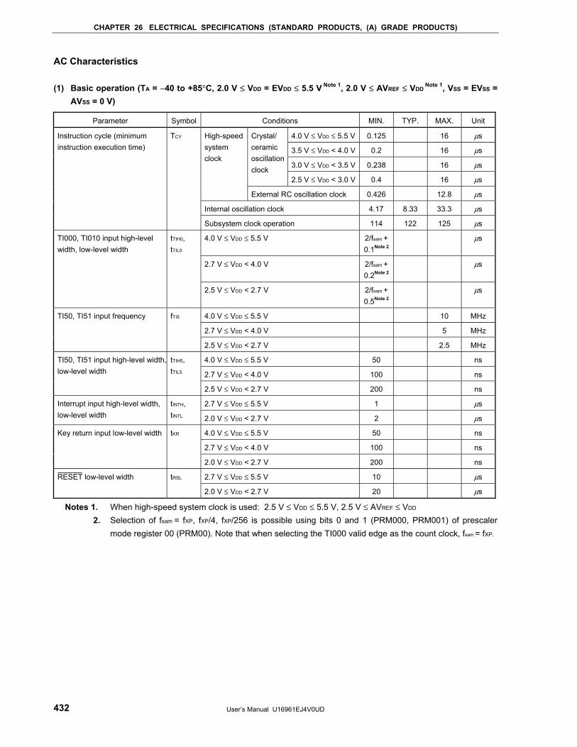
CHAPTER 26 ELECTRICAL SPECIFICATIONS (STANDARD PRODUCTS, (A) GRADE PRODUCTS)
User’s Manual U16961EJ4V0UD 432
AC Characteristics (1) Basic operation (TA = −40 to +85°C, 2.0 V ≤ VDD = EVDD ≤ 5.5 V Note 1, 2.0 V ≤ AVREF ≤ VDD
Note 1, VSS = EVSS = AVSS = 0 V)
Parameter Symbol Conditions MIN. TYP. MAX. Unit
4.0 V ≤ VDD ≤ 5.5 V 0.125 16 μs
3.5 V ≤ VDD < 4.0 V 0.2 16 μs
3.0 V ≤ VDD < 3.5 V 0.238 16 μs
Crystal/ ceramic oscillation clock
2.5 V ≤ VDD < 3.0 V 0.4 16 μs
High-speed system clock
External RC oscillation clock 0.426 12.8 μs
Internal oscillation clock 4.17 8.33 33.3 μs
Instruction cycle (minimum instruction execution time)
TCY
Subsystem clock operation 114 122 125 μs
4.0 V ≤ VDD ≤ 5.5 V 2/fsam +0.1Note 2
μs
2.7 V ≤ VDD < 4.0 V 2/fsam +0.2Note 2
μs
TI000, TI010 input high-level width, low-level width
tTIH0, tTIL0
2.5 V ≤ VDD < 2.7 V 2/fsam +0.5Note 2
μs
4.0 V ≤ VDD ≤ 5.5 V 10 MHz
2.7 V ≤ VDD < 4.0 V 5 MHz
TI50, TI51 input frequency fTI5
2.5 V ≤ VDD < 2.7 V 2.5 MHz
4.0 V ≤ VDD ≤ 5.5 V 50 ns
2.7 V ≤ VDD < 4.0 V 100 ns
TI50, TI51 input high-level width, low-level width
tTIH5, tTIL5
2.5 V ≤ VDD < 2.7 V 200 ns
2.7 V ≤ VDD ≤ 5.5 V 1 μs Interrupt input high-level width, low-level width
tINTH, tINTL 2.0 V ≤ VDD < 2.7 V 2 μs
4.0 V ≤ VDD ≤ 5.5 V 50 ns
2.7 V ≤ VDD < 4.0 V 100 ns
Key return input low-level width tKR
2.0 V ≤ VDD < 2.7 V 200 ns
2.7 V ≤ VDD ≤ 5.5 V 10 μs RESET low-level width tRSL
2.0 V ≤ VDD < 2.7 V 20 μs
Notes 1. When high-speed system clock is used: 2.5 V ≤ VDD ≤ 5.5 V, 2.5 V ≤ AVREF ≤ VDD 2. Selection of fsam = fXP, fXP/4, fXP/256 is possible using bits 0 and 1 (PRM000, PRM001) of prescaler
mode register 00 (PRM00). Note that when selecting the TI000 valid edge as the count clock, fsam = fXP.
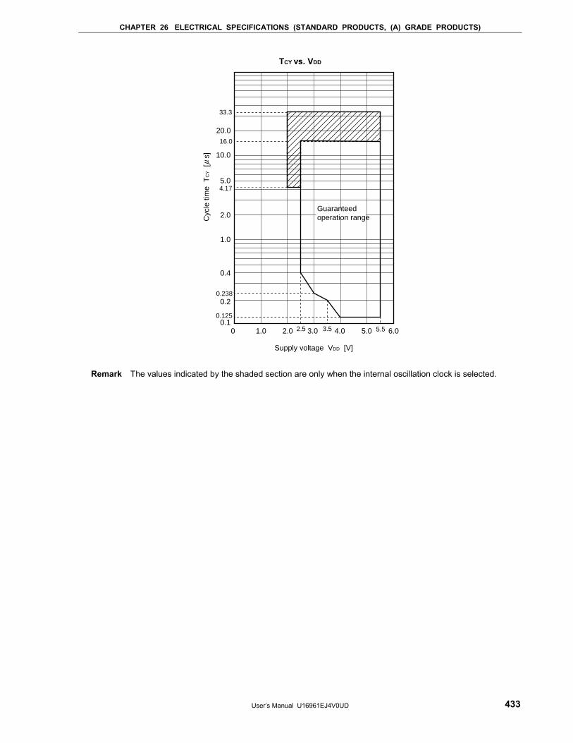
CHAPTER 26 ELECTRICAL SPECIFICATIONS (STANDARD PRODUCTS, (A) GRADE PRODUCTS)
User’s Manual U16961EJ4V0UD 433
TCY vs. VDD
5.0
1.0
2.0
0.4
0.2
0.10
10.0
1.0 2.0 3.0 4.0 5.0 6.05.5
20.016.0
33.3
4.17
0.238
0.125
3.52.5
Supply voltage VDD [V]
Cyc
le ti
me
TC
Y [
s]
Guaranteed operation range
μ
Remark The values indicated by the shaded section are only when the internal oscillation clock is selected.
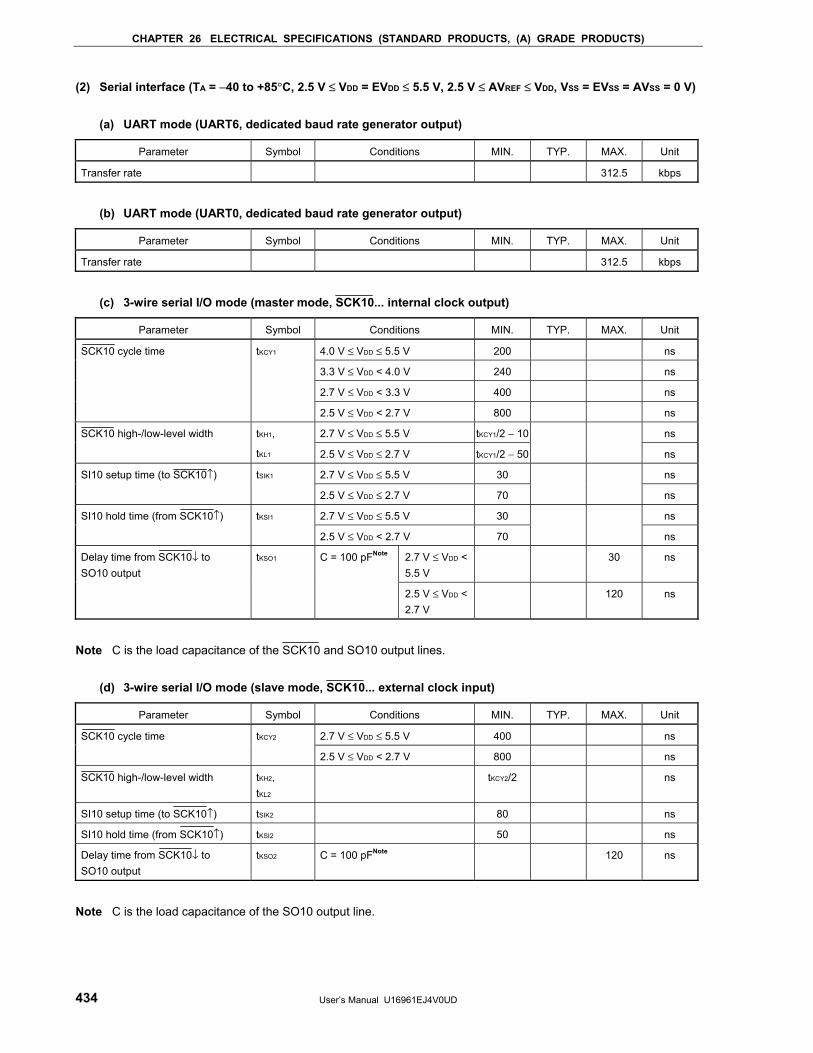
CHAPTER 26 ELECTRICAL SPECIFICATIONS (STANDARD PRODUCTS, (A) GRADE PRODUCTS)
User’s Manual U16961EJ4V0UD 434
(2) Serial interface (TA = −40 to +85°C, 2.5 V ≤ VDD = EVDD ≤ 5.5 V, 2.5 V ≤ AVREF ≤ VDD, VSS = EVSS = AVSS = 0 V)
(a) UART mode (UART6, dedicated baud rate generator output)
Parameter Symbol Conditions MIN. TYP. MAX. Unit
Transfer rate 312.5 kbps
(b) UART mode (UART0, dedicated baud rate generator output)
Parameter Symbol Conditions MIN. TYP. MAX. Unit
Transfer rate 312.5 kbps
(c) 3-wire serial I/O mode (master mode, SCK10... internal clock output)
Parameter Symbol Conditions MIN. TYP. MAX. Unit
4.0 V ≤ VDD ≤ 5.5 V 200 ns
3.3 V ≤ VDD < 4.0 V 240 ns
2.7 V ≤ VDD < 3.3 V 400 ns
SCK10 cycle time tKCY1
2.5 V ≤ VDD < 2.7 V 800 ns
2.7 V ≤ VDD ≤ 5.5 V tKCY1/2 − 10 ns SCK10 high-/low-level width tKH1,
tKL1 2.5 V ≤ VDD ≤ 2.7 V tKCY1/2 − 50
ns
2.7 V ≤ VDD ≤ 5.5 V 30 ns SI10 setup time (to SCK10↑) tSIK1
2.5 V ≤ VDD ≤ 2.7 V 70
ns
2.7 V ≤ VDD ≤ 5.5 V 30 ns SI10 hold time (from SCK10↑) tKSI1
2.5 V ≤ VDD < 2.7 V 70
ns
2.7 V ≤ VDD < 5.5 V
30 ns Delay time from SCK10↓ to SO10 output
tKSO1 C = 100 pFNote
2.5 V ≤ VDD < 2.7 V
120 ns
Note C is the load capacitance of the SCK10 and SO10 output lines.
(d) 3-wire serial I/O mode (slave mode, SCK10... external clock input)
Parameter Symbol Conditions MIN. TYP. MAX. Unit
2.7 V ≤ VDD ≤ 5.5 V 400 ns SCK10 cycle time tKCY2
2.5 V ≤ VDD < 2.7 V 800 ns
SCK10 high-/low-level width tKH2, tKL2
tKCY2/2 ns
SI10 setup time (to SCK10↑) tSIK2 80 ns
SI10 hold time (from SCK10↑) tKSI2 50 ns
Delay time from SCK10↓ to SO10 output
tKSO2 C = 100 pFNote 120 ns
Note C is the load capacitance of the SO10 output line.
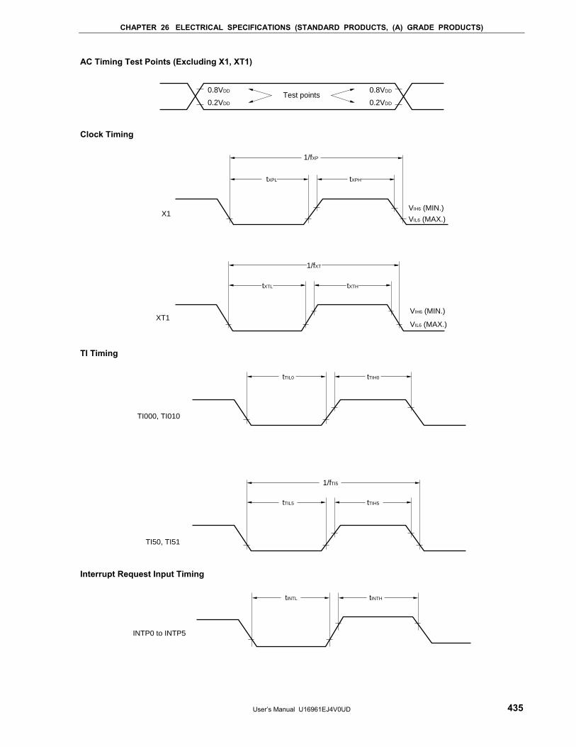
CHAPTER 26 ELECTRICAL SPECIFICATIONS (STANDARD PRODUCTS, (A) GRADE PRODUCTS)
User’s Manual U16961EJ4V0UD 435
AC Timing Test Points (Excluding X1, XT1)
0.8VDD
0.2VDD
Test points0.8VDD
0.2VDD
Clock Timing
X1VIH6 (MIN.)
VIL6 (MAX.)
1/fXP
tXPL tXPH
1/fXT
tXTL tXTH
XT1VIH6 (MIN.)
VIL6 (MAX.) TI Timing
TI000, TI010
tTIL0 tTIH0
TI50, TI51
1/fTI5
tTIL5 tTIH5
Interrupt Request Input Timing
INTP0 to INTP5
tINTL tINTH
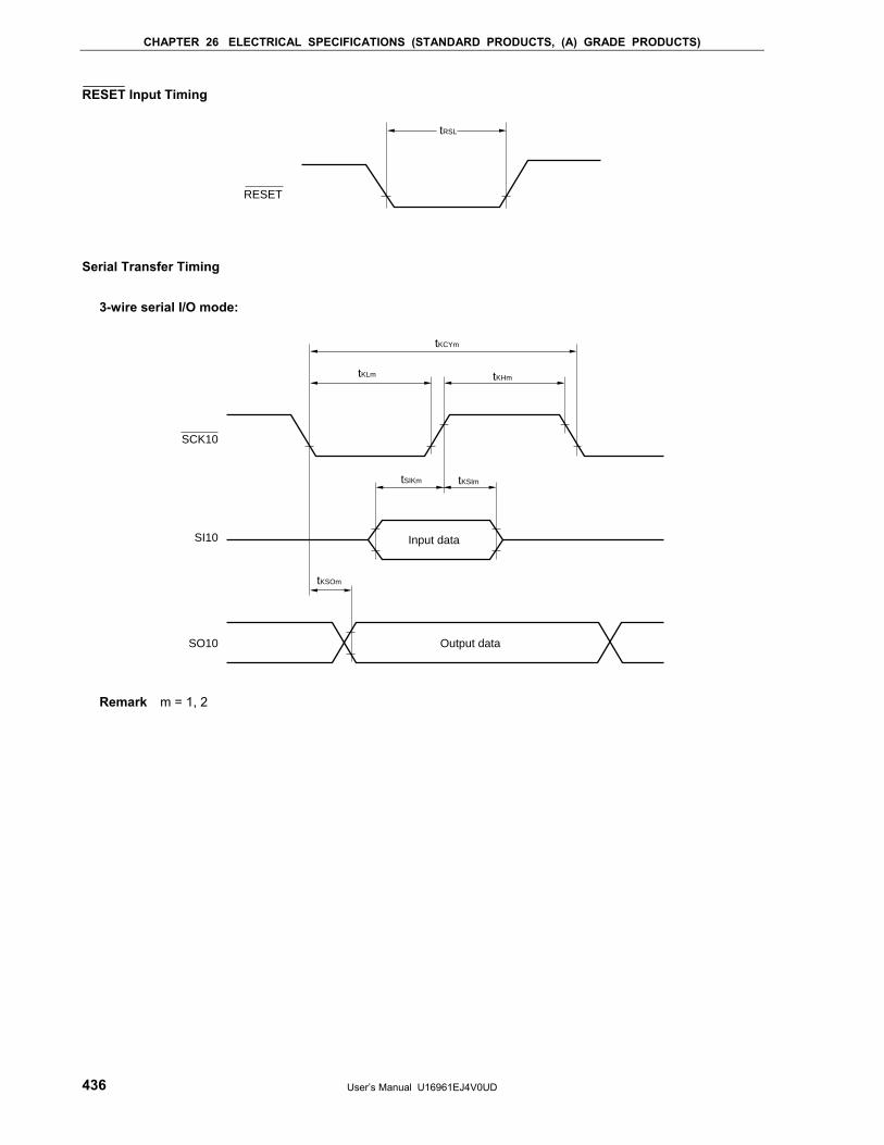
CHAPTER 26 ELECTRICAL SPECIFICATIONS (STANDARD PRODUCTS, (A) GRADE PRODUCTS)
User’s Manual U16961EJ4V0UD 436
RESET Input Timing
RESET
tRSL
Serial Transfer Timing
3-wire serial I/O mode:
SI10
SO10
tKCYm
tKLm tKHm
tSIKm tKSIm
Input data
tKSOm
Output data
SCK10
Remark m = 1, 2
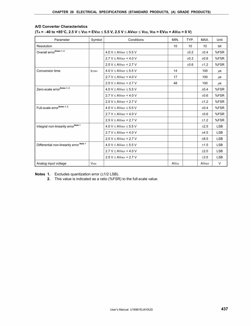
CHAPTER 26 ELECTRICAL SPECIFICATIONS (STANDARD PRODUCTS, (A) GRADE PRODUCTS)
User’s Manual U16961EJ4V0UD 437
A/D Converter Characteristics (TA = −40 to +85°C, 2.5 V ≤ VDD = EVDD ≤ 5.5 V, 2.5 V ≤ AVREF ≤ VDD, VSS = EVSS = AVSS = 0 V)
Parameter Symbol Conditions MIN. TYP. MAX. Unit
Resolution 10 10 10 bit
4.0 V ≤ AVREF ≤ 5.5 V ±0.2 ±0.4 %FSR
2.7 V ≤ AVREF < 4.0 V ±0.3 ±0.6 %FSR
Overall errorNotes 1, 2
2.5 V ≤ AVREF < 2.7 V ±0.6 ±1.2 %FSR
4.0 V ≤ AVREF ≤ 5.5 V 14 100 μs
2.7 V ≤ AVREF < 4.0 V 17 100 μs
Conversion time tCONV
2.5 V ≤ AVREF < 2.7 V 48 100 μs
4.0 V ≤ AVREF ≤ 5.5 V ±0.4 %FSR
2.7 V ≤ AVREF < 4.0 V ±0.6 %FSR
Zero-scale errorNotes 1, 2
2.5 V ≤ AVREF < 2.7 V ±1.2 %FSR
4.0 V ≤ AVREF ≤ 5.5 V ±0.4 %FSR
2.7 V ≤ AVREF < 4.0 V ±0.6 %FSR
Full-scale errorNotes 1, 2
2.5 V ≤ AVREF < 2.7 V ±1.2 %FSR
4.0 V ≤ AVREF ≤ 5.5 V ±2.5 LSB
2.7 V ≤ AVREF < 4.0 V ±4.5 LSB
Integral non-linearity errorNote 1
2.5 V ≤ AVREF < 2.7 V ±8.5 LSB
4.0 V ≤ AVREF ≤ 5.5 V ±1.5 LSB
2.7 V ≤ AVREF < 4.0 V ±2.0 LSB
Differential non-linearity error Note 1
2.5 V ≤ AVREF < 2.7 V ±3.5 LSB
Analog input voltage VAIN AVSS AVREF V
Notes 1. Excludes quantization error (±1/2 LSB). 2. This value is indicated as a ratio (%FSR) to the full-scale value.
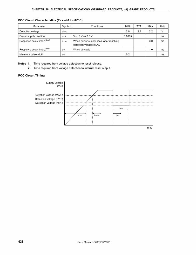
CHAPTER 26 ELECTRICAL SPECIFICATIONS (STANDARD PRODUCTS, (A) GRADE PRODUCTS)
User’s Manual U16961EJ4V0UD 438
POC Circuit Characteristics (TA = −40 to +85°C)
Parameter Symbol Conditions MIN. TYP. MAX. Unit
Detection voltage VPOC 2.0 2.1 2.2 V
Power supply rise time tPTH VDD: 0 V → 2.0 V 0.0015 ms
Response delay time 1Note1 tPTHD When power supply rises, after reaching detection voltage (MAX.)
3.0 ms
Response delay time 2Note2 tPD When VDD falls 1.0 ms
Minimum pulse width tPW 0.2 ms
Notes 1. Time required from voltage detection to reset release. 2. Time required from voltage detection to internal reset output. POC Circuit Timing
Supply voltage(VDD)
Time
Detection voltage (MIN.)
Detection voltage (TYP.)
Detection voltage (MAX.)
tPTH tPTHD
tPW
tPD

CHAPTER 26 ELECTRICAL SPECIFICATIONS (STANDARD PRODUCTS, (A) GRADE PRODUCTS)
User’s Manual U16961EJ4V0UD 439
LVI Circuit Characteristics (TA = −40 to +85°C)
Parameter Symbol Conditions MIN. TYP. MAX. Unit
VLVI0 4.1 4.3 4.5 V
VLVI1 3.9 4.1 4.3 V
VLVI2 3.7 3.9 4.1 V
VLVI3 3.5 3.7 3.9 V
VLVI4 3.3 3.5 3.7 V
VLVI5 3.15 3.3 3.45 V
VLVI6 2.95 3.1 3.25 V
VLVI7 2.7 2.85 3.0 V
VLVI8 2.5 2.6 2.7 V
Detection voltage
VLVI9 2.25 2.35 2.45 V
Response timeNote 1 tLD 0.2 2.0 ms
Minimum pulse width tLW 0.2 ms
Operation stabilization wait timeNote
2 tLWAIT 0.1 0.2 ms
Notes 1. Time required from voltage detection to interrupt output or internal reset output. 2. Time required from setting LVION to 1 to operation stabilization. Remarks 1. VLVI0 > VLVI1 > VLVI2 > VLVI3 > VLVI4 > VLVI5 > VLVI6 > VLVI7 > VLVI8 > VLVI9 2. VPOC < VLVIm (m = 0 to 9) LVI Circuit Timing
Supply voltage(VDD)
Time
Detection voltage (MIN.)
Detection voltage (TYP.)
Detection voltage (MAX.)
tLW
tLDtLWAIT
LVION ← 1 Data Memory STOP Mode Low Supply Voltage Data Retention Characteristics (TA = −40 to +85°C)
Parameter Symbol Conditions MIN. TYP. MAX. Unit
Data retention supply voltage VDDDR 2.0 5.5 V
Release signal set time tSREL 0 μs
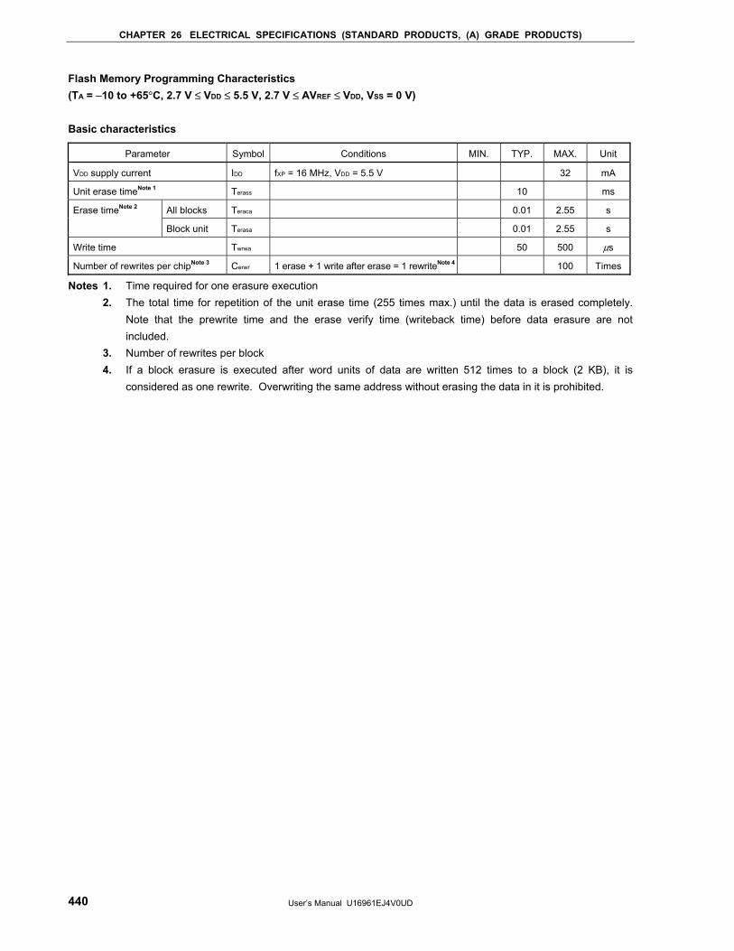
CHAPTER 26 ELECTRICAL SPECIFICATIONS (STANDARD PRODUCTS, (A) GRADE PRODUCTS)
User’s Manual U16961EJ4V0UD 440
Flash Memory Programming Characteristics (TA = −10 to +65°C, 2.7 V ≤ VDD ≤ 5.5 V, 2.7 V ≤ AVREF ≤ VDD, VSS = 0 V) Basic characteristics
Parameter Symbol Conditions MIN. TYP. MAX. Unit
VDD supply current IDD fXP = 16 MHz, VDD = 5.5 V 32 mA
Unit erase timeNote 1 Terass 10 ms
All blocks Teraca 0.01 2.55 s Erase timeNote 2
Block unit Terasa 0.01 2.55 s
Write time Twrwa 50 500 μs
Number of rewrites per chipNote 3 Cerwr 1 erase + 1 write after erase = 1 rewriteNote 4 100 Times
Notes 1. Time required for one erasure execution 2. The total time for repetition of the unit erase time (255 times max.) until the data is erased completely.
Note that the prewrite time and the erase verify time (writeback time) before data erasure are not included.
3. Number of rewrites per block 4. If a block erasure is executed after word units of data are written 512 times to a block (2 KB), it is
considered as one rewrite. Overwriting the same address without erasing the data in it is prohibited.
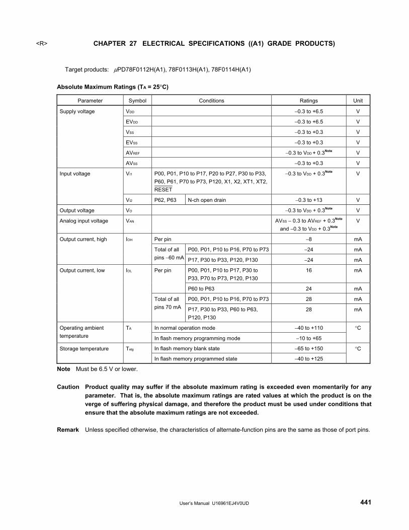
User’s Manual U16961EJ4V0UD 441
CHAPTER 27 ELECTRICAL SPECIFICATIONS ((A1) GRADE PRODUCTS)
Target products: μPD78F0112H(A1), 78F0113H(A1), 78F0114H(A1)
Absolute Maximum Ratings (TA = 25°C)
Parameter Symbol Conditions Ratings Unit
VDD −0.3 to +6.5 V
EVDD −0.3 to +6.5 V
VSS −0.3 to +0.3 V
EVSS −0.3 to +0.3 V
AVREF −0.3 to VDD + 0.3Note V
Supply voltage
AVSS −0.3 to +0.3 V
VI1 P00, P01, P10 to P17, P20 to P27, P30 to P33, P60, P61, P70 to P73, P120, X1, X2, XT1, XT2, RESET
−0.3 to VDD + 0.3Note V Input voltage
VI2 P62, P63 N-ch open drain −0.3 to +13 V
Output voltage VO −0.3 to VDD + 0.3Note V
Analog input voltage VAN AVSS − 0.3 to AVREF + 0.3Note
and −0.3 to VDD + 0.3Note V
Per pin −8 mA
P00, P01, P10 to P16, P70 to P73 −24 mA
Output current, high IOH
Total of all pins −60 mA P17, P30 to P33, P120, P130 −24 mA
P00, P01, P10 to P17, P30 to P33, P70 to P73, P120, P130
16 mA Per pin
P60 to P63 24 mA
P00, P01, P10 to P16, P70 to P73 28 mA
Output current, low IOL
Total of all pins 70 mA P17, P30 to P33, P60 to P63,
P120, P130 28 mA
In normal operation mode −40 to +110 Operating ambient temperature
TA
In flash memory programming mode −10 to +65
°C
In flash memory blank state −65 to +150 Storage temperature Tstg
In flash memory programmed state −40 to +125
°C
Note Must be 6.5 V or lower. Caution Product quality may suffer if the absolute maximum rating is exceeded even momentarily for any
parameter. That is, the absolute maximum ratings are rated values at which the product is on the verge of suffering physical damage, and therefore the product must be used under conditions that ensure that the absolute maximum ratings are not exceeded.
Remark Unless specified otherwise, the characteristics of alternate-function pins are the same as those of port pins.
<R>
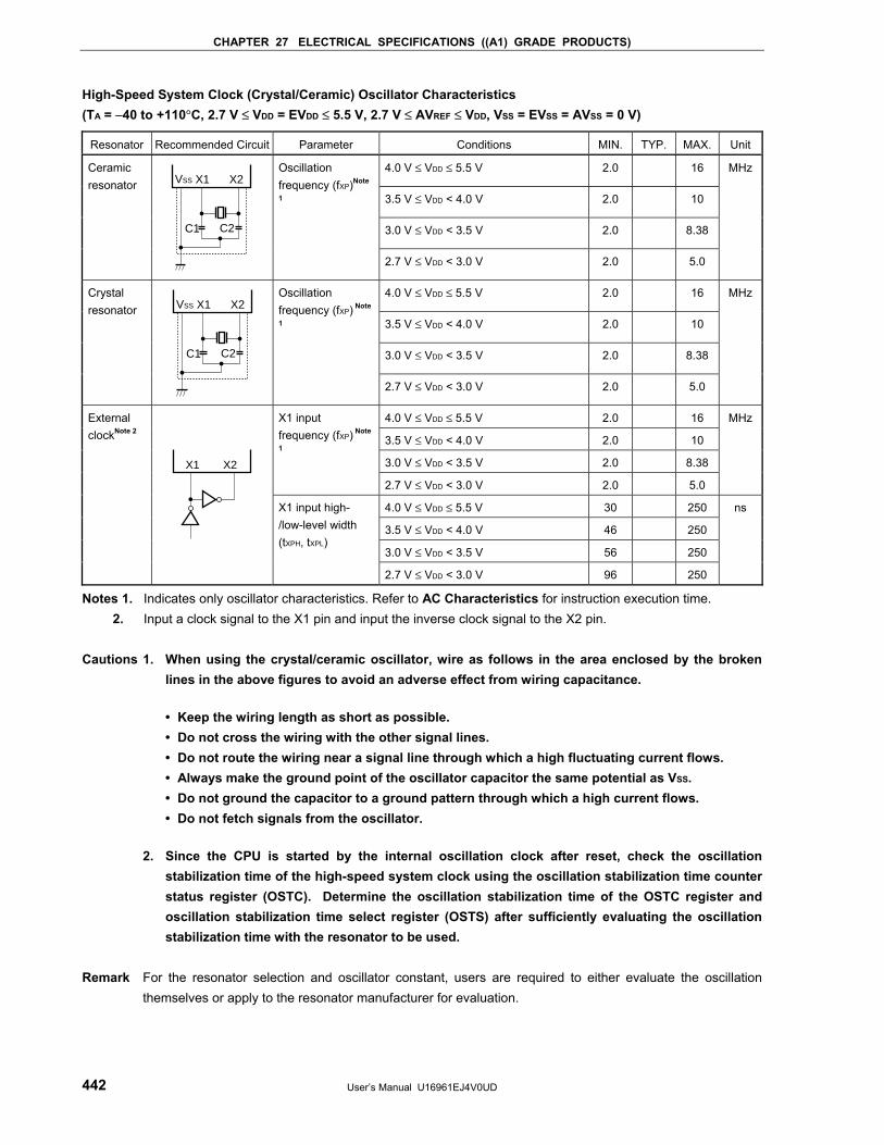
CHAPTER 27 ELECTRICAL SPECIFICATIONS ((A1) GRADE PRODUCTS)
User’s Manual U16961EJ4V0UD 442
High-Speed System Clock (Crystal/Ceramic) Oscillator Characteristics (TA = −40 to +110°C, 2.7 V ≤ VDD = EVDD ≤ 5.5 V, 2.7 V ≤ AVREF ≤ VDD, VSS = EVSS = AVSS = 0 V)
Resonator Recommended Circuit Parameter Conditions MIN. TYP. MAX. Unit
4.0 V ≤ VDD ≤ 5.5 V 2.0 16
3.5 V ≤ VDD < 4.0 V 2.0 10
3.0 V ≤ VDD < 3.5 V 2.0 8.38
Ceramic resonator
C1
X2X1VSS
C2
Oscillation frequency (fXP)Note
1
2.7 V ≤ VDD < 3.0 V 2.0 5.0
MHz
4.0 V ≤ VDD ≤ 5.5 V 2.0 16
3.5 V ≤ VDD < 4.0 V 2.0 10
3.0 V ≤ VDD < 3.5 V 2.0 8.38
Crystal resonator
C1
X2X1VSS
C2
Oscillation frequency (fXP) Note
1
2.7 V ≤ VDD < 3.0 V 2.0 5.0
MHz
4.0 V ≤ VDD ≤ 5.5 V 2.0 16
3.5 V ≤ VDD < 4.0 V 2.0 10
3.0 V ≤ VDD < 3.5 V 2.0 8.38
X1 input frequency (fXP) Note
1
2.7 V ≤ VDD < 3.0 V 2.0 5.0
MHz
4.0 V ≤ VDD ≤ 5.5 V 30 250
3.5 V ≤ VDD < 4.0 V 46 250
3.0 V ≤ VDD < 3.5 V 56 250
External clockNote 2
X2X1
X1 input high-/low-level width (tXPH, tXPL)
2.7 V ≤ VDD < 3.0 V 96 250
ns
Notes 1. Indicates only oscillator characteristics. Refer to AC Characteristics for instruction execution time. 2. Input a clock signal to the X1 pin and input the inverse clock signal to the X2 pin.
Cautions 1. When using the crystal/ceramic oscillator, wire as follows in the area enclosed by the broken
lines in the above figures to avoid an adverse effect from wiring capacitance. • Keep the wiring length as short as possible. • Do not cross the wiring with the other signal lines. • Do not route the wiring near a signal line through which a high fluctuating current flows. • Always make the ground point of the oscillator capacitor the same potential as VSS. • Do not ground the capacitor to a ground pattern through which a high current flows. • Do not fetch signals from the oscillator. 2. Since the CPU is started by the internal oscillation clock after reset, check the oscillation
stabilization time of the high-speed system clock using the oscillation stabilization time counter status register (OSTC). Determine the oscillation stabilization time of the OSTC register and oscillation stabilization time select register (OSTS) after sufficiently evaluating the oscillation stabilization time with the resonator to be used.
Remark For the resonator selection and oscillator constant, users are required to either evaluate the oscillation
themselves or apply to the resonator manufacturer for evaluation.
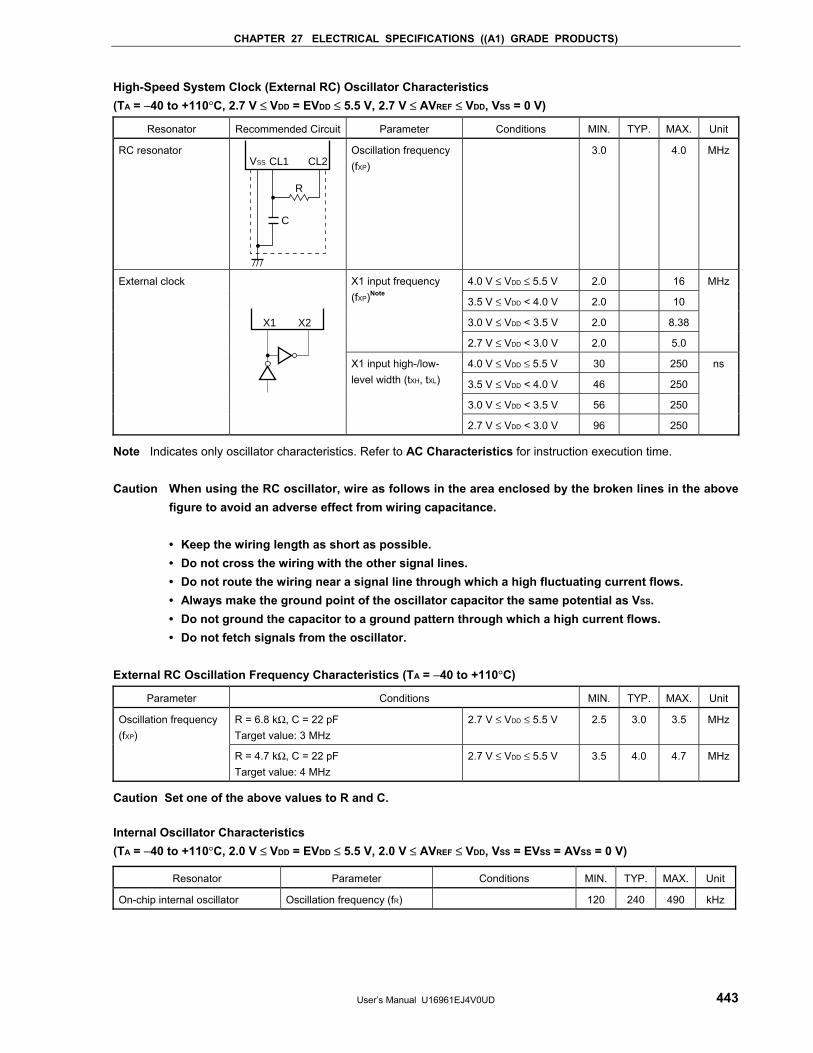
CHAPTER 27 ELECTRICAL SPECIFICATIONS ((A1) GRADE PRODUCTS)
User’s Manual U16961EJ4V0UD 443
High-Speed System Clock (External RC) Oscillator Characteristics (TA = −40 to +110°C, 2.7 V ≤ VDD = EVDD ≤ 5.5 V, 2.7 V ≤ AVREF ≤ VDD, VSS = 0 V)
Resonator Recommended Circuit Parameter Conditions MIN. TYP. MAX. Unit
RC resonator VSS CL1 CL2
R
C
Oscillation frequency (fXP)
3.0 4.0 MHz
4.0 V ≤ VDD ≤ 5.5 V 2.0 16
3.5 V ≤ VDD < 4.0 V 2.0 10
3.0 V ≤ VDD < 3.5 V 2.0 8.38
X1 input frequency (fXP)Note
2.7 V ≤ VDD < 3.0 V 2.0 5.0
MHz
4.0 V ≤ VDD ≤ 5.5 V 30 250
3.5 V ≤ VDD < 4.0 V 46 250
3.0 V ≤ VDD < 3.5 V 56 250
External clock
X2X1
X1 input high-/low-level width (tXH, tXL)
2.7 V ≤ VDD < 3.0 V 96 250
ns
Note Indicates only oscillator characteristics. Refer to AC Characteristics for instruction execution time. Caution When using the RC oscillator, wire as follows in the area enclosed by the broken lines in the above
figure to avoid an adverse effect from wiring capacitance. • Keep the wiring length as short as possible. • Do not cross the wiring with the other signal lines. • Do not route the wiring near a signal line through which a high fluctuating current flows. • Always make the ground point of the oscillator capacitor the same potential as VSS. • Do not ground the capacitor to a ground pattern through which a high current flows. • Do not fetch signals from the oscillator. External RC Oscillation Frequency Characteristics (TA = −40 to +110°C)
Parameter Conditions MIN. TYP. MAX. Unit
R = 6.8 kΩ, C = 22 pF Target value: 3 MHz
2.7 V ≤ VDD ≤ 5.5 V 2.5 3.0 3.5 MHz Oscillation frequency (fXP)
R = 4.7 kΩ, C = 22 pF Target value: 4 MHz
2.7 V ≤ VDD ≤ 5.5 V 3.5 4.0 4.7 MHz
Caution Set one of the above values to R and C. Internal Oscillator Characteristics (TA = −40 to +110°C, 2.0 V ≤ VDD = EVDD ≤ 5.5 V, 2.0 V ≤ AVREF ≤ VDD, VSS = EVSS = AVSS = 0 V)
Resonator Parameter Conditions MIN. TYP. MAX. Unit
On-chip internal oscillator Oscillation frequency (fR) 120 240 490 kHz
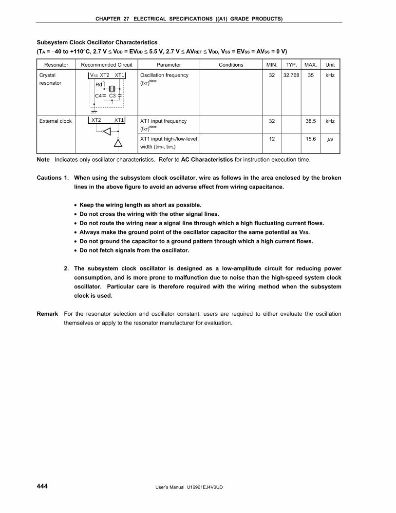
CHAPTER 27 ELECTRICAL SPECIFICATIONS ((A1) GRADE PRODUCTS)
User’s Manual U16961EJ4V0UD 444
Subsystem Clock Oscillator Characteristics (TA = −40 to +110°C, 2.7 V ≤ VDD = EVDD ≤ 5.5 V, 2.7 V ≤ AVREF ≤ VDD, VSS = EVSS = AVSS = 0 V)
Resonator Recommended Circuit Parameter Conditions MIN. TYP. MAX. Unit
Crystal resonator
XT1VSS XT2
C4 C3
Rd
Oscillation frequency (fXT)Note
32 32.768 35 kHz
XT1 input frequency (fXT)Note
32 38.5 kHz External clock XT1XT2
XT1 input high-/low-level width (tXTH, tXTL)
12 15.6 μs
Note Indicates only oscillator characteristics. Refer to AC Characteristics for instruction execution time. Cautions 1. When using the subsystem clock oscillator, wire as follows in the area enclosed by the broken
lines in the above figure to avoid an adverse effect from wiring capacitance. • Keep the wiring length as short as possible. • Do not cross the wiring with the other signal lines. • Do not route the wiring near a signal line through which a high fluctuating current flows. • Always make the ground point of the oscillator capacitor the same potential as VSS. • Do not ground the capacitor to a ground pattern through which a high current flows. • Do not fetch signals from the oscillator. 2. The subsystem clock oscillator is designed as a low-amplitude circuit for reducing power
consumption, and is more prone to malfunction due to noise than the high-speed system clock oscillator. Particular care is therefore required with the wiring method when the subsystem clock is used.
Remark For the resonator selection and oscillator constant, users are required to either evaluate the oscillation
themselves or apply to the resonator manufacturer for evaluation.
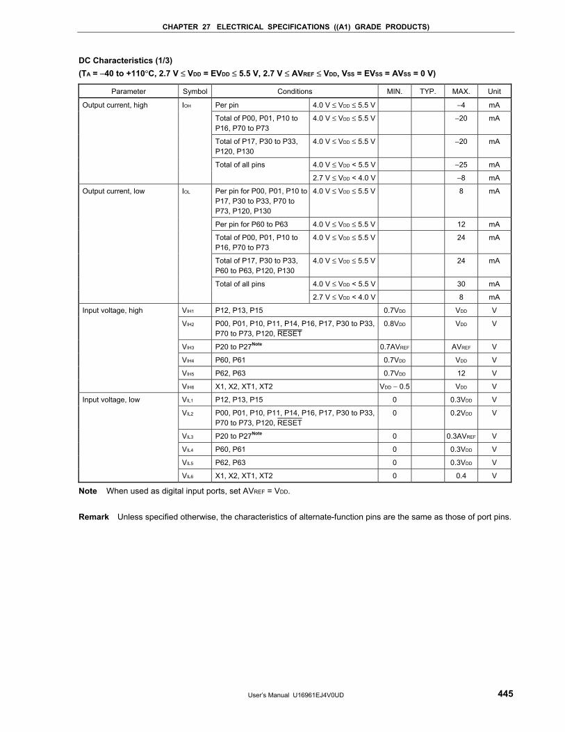
CHAPTER 27 ELECTRICAL SPECIFICATIONS ((A1) GRADE PRODUCTS)
User’s Manual U16961EJ4V0UD 445
DC Characteristics (1/3) (TA = −40 to +110°C, 2.7 V ≤ VDD = EVDD ≤ 5.5 V, 2.7 V ≤ AVREF ≤ VDD, VSS = EVSS = AVSS = 0 V)
Parameter Symbol Conditions MIN. TYP. MAX. Unit
Per pin 4.0 V ≤ VDD ≤ 5.5 V −4 mA
Total of P00, P01, P10 to P16, P70 to P73
4.0 V ≤ VDD ≤ 5.5 V −20 mA
Total of P17, P30 to P33, P120, P130
4.0 V ≤ VDD ≤ 5.5 V −20 mA
4.0 V ≤ VDD < 5.5 V −25 mA
Output current, high IOH
Total of all pins
2.7 V ≤ VDD < 4.0 V −8 mA
Per pin for P00, P01, P10 to P17, P30 to P33, P70 to P73, P120, P130
4.0 V ≤ VDD ≤ 5.5 V 8 mA
Per pin for P60 to P63 4.0 V ≤ VDD ≤ 5.5 V 12 mA
Total of P00, P01, P10 to P16, P70 to P73
4.0 V ≤ VDD ≤ 5.5 V 24 mA
Total of P17, P30 to P33, P60 to P63, P120, P130
4.0 V ≤ VDD ≤ 5.5 V 24 mA
4.0 V ≤ VDD < 5.5 V 30 mA
Output current, low IOL
Total of all pins
2.7 V ≤ VDD < 4.0 V 8 mA
VIH1 P12, P13, P15 0.7VDD VDD V
VIH2 P00, P01, P10, P11, P14, P16, P17, P30 to P33, P70 to P73, P120, RESET
0.8VDD VDD V
VIH3 P20 to P27Note 0.7AVREF AVREF V
VIH4 P60, P61 0.7VDD VDD V
VIH5 P62, P63 0.7VDD 12 V
Input voltage, high
VIH6 X1, X2, XT1, XT2 VDD − 0.5 VDD V
VIL1 P12, P13, P15 0 0.3VDD V
VIL2 P00, P01, P10, P11, P14, P16, P17, P30 to P33, P70 to P73, P120, RESET
0 0.2VDD V
VIL3 P20 to P27Note 0 0.3AVREF V
VIL4 P60, P61 0 0.3VDD V
VIL5 P62, P63 0 0.3VDD V
Input voltage, low
VIL6 X1, X2, XT1, XT2 0 0.4 V
Note When used as digital input ports, set AVREF = VDD. Remark Unless specified otherwise, the characteristics of alternate-function pins are the same as those of port pins.
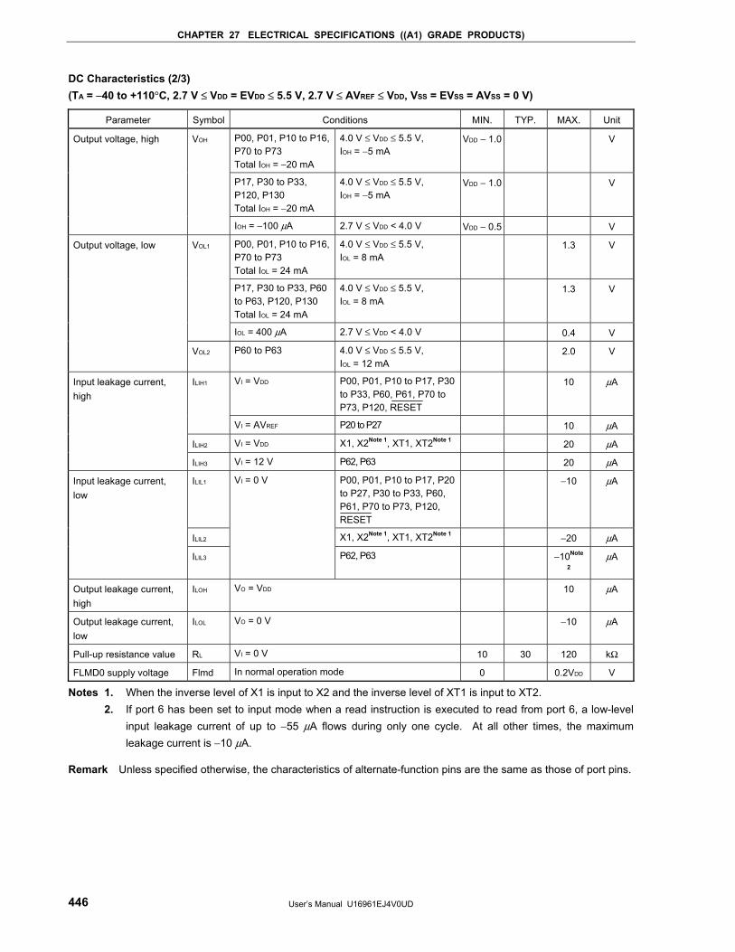
CHAPTER 27 ELECTRICAL SPECIFICATIONS ((A1) GRADE PRODUCTS)
User’s Manual U16961EJ4V0UD 446
DC Characteristics (2/3) (TA = −40 to +110°C, 2.7 V ≤ VDD = EVDD ≤ 5.5 V, 2.7 V ≤ AVREF ≤ VDD, VSS = EVSS = AVSS = 0 V)
Parameter Symbol Conditions MIN. TYP. MAX. Unit
P00, P01, P10 to P16, P70 to P73 Total IOH = −20 mA
4.0 V ≤ VDD ≤ 5.5 V, IOH = −5 mA
VDD − 1.0 V
P17, P30 to P33, P120, P130 Total IOH = −20 mA
4.0 V ≤ VDD ≤ 5.5 V, IOH = −5 mA
VDD − 1.0 V
Output voltage, high VOH
IOH = −100 μA 2.7 V ≤ VDD < 4.0 V VDD − 0.5 V
P00, P01, P10 to P16, P70 to P73 Total IOL = 24 mA
4.0 V ≤ VDD ≤ 5.5 V, IOL = 8 mA
1.3 V
P17, P30 to P33, P60 to P63, P120, P130 Total IOL = 24 mA
4.0 V ≤ VDD ≤ 5.5 V, IOL = 8 mA
1.3 V
VOL1
IOL = 400 μA 2.7 V ≤ VDD < 4.0 V 0.4 V
Output voltage, low
VOL2 P60 to P63 4.0 V ≤ VDD ≤ 5.5 V, IOL = 12 mA
2.0 V
VI = VDD P00, P01, P10 to P17, P30 to P33, P60, P61, P70 to P73, P120, RESET
10 μA ILIH1
VI = AVREF P20 to P27 10 μA
ILIH2 VI = VDD X1, X2Note 1, XT1, XT2Note 1 20 μA
Input leakage current, high
ILIH3 VI = 12 V P62, P63 20 μA
ILIL1 P00, P01, P10 to P17, P20 to P27, P30 to P33, P60, P61, P70 to P73, P120, RESET
−10 μA
ILIL2 X1, X2Note 1, XT1, XT2Note 1 −20 μA
Input leakage current, low
ILIL3
VI = 0 V
P62, P63 −10Note
2 μA
Output leakage current, high
ILOH VO = VDD 10 μA
Output leakage current, low
ILOL VO = 0 V −10 μA
Pull-up resistance value RL VI = 0 V 10 30 120 kΩ
FLMD0 supply voltage Flmd In normal operation mode 0 0.2VDD V
Notes 1. When the inverse level of X1 is input to X2 and the inverse level of XT1 is input to XT2. 2. If port 6 has been set to input mode when a read instruction is executed to read from port 6, a low-level
input leakage current of up to −55 μA flows during only one cycle. At all other times, the maximum leakage current is −10 μA.
Remark Unless specified otherwise, the characteristics of alternate-function pins are the same as those of port pins.
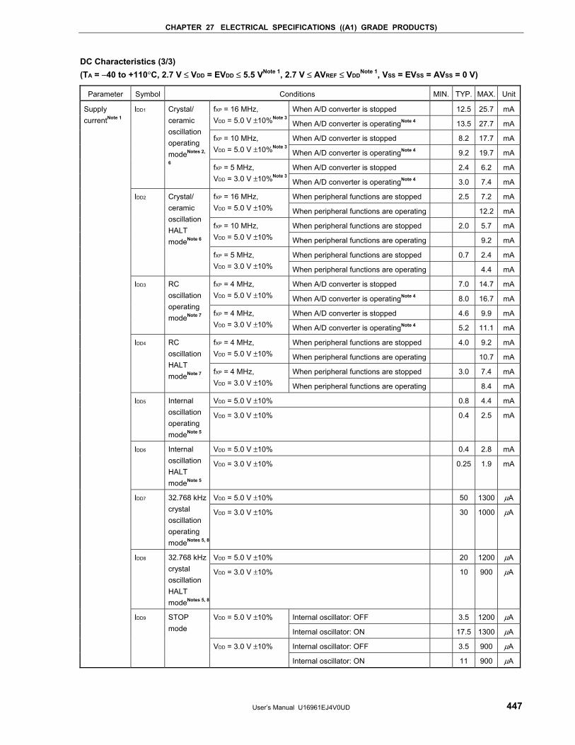
CHAPTER 27 ELECTRICAL SPECIFICATIONS ((A1) GRADE PRODUCTS)
User’s Manual U16961EJ4V0UD 447
DC Characteristics (3/3) (TA = −40 to +110°C, 2.7 V ≤ VDD = EVDD ≤ 5.5 VNote 1, 2.7 V ≤ AVREF ≤ VDD
Note 1, VSS = EVSS = AVSS = 0 V)
Parameter Symbol Conditions MIN. TYP. MAX. Unit
When A/D converter is stopped 12.5 25.7 mA fXP = 16 MHz, VDD = 5.0 V ±10%Note 3
When A/D converter is operatingNote 4 13.5 27.7 mA
When A/D converter is stopped 8.2 17.7 mA fXP = 10 MHz, VDD = 5.0 V ±10%Note 3
When A/D converter is operatingNote 4 9.2 19.7 mA
When A/D converter is stopped 2.4 6.2 mA
IDD1 Crystal/ ceramic oscillation operating modeNotes 2,
6 fXP = 5 MHz, VDD = 3.0 V ±10%Note 3
When A/D converter is operatingNote 4 3.0 7.4 mA
When peripheral functions are stopped 2.5 7.2 mA fXP = 16 MHz, VDD = 5.0 V ±10% When peripheral functions are operating 12.2 mA
When peripheral functions are stopped 2.0 5.7 mA fXP = 10 MHz, VDD = 5.0 V ±10% When peripheral functions are operating 9.2 mA
When peripheral functions are stopped 0.7 2.4 mA
IDD2 Crystal/ ceramic oscillation HALT modeNote 6
fXP = 5 MHz, VDD = 3.0 V ±10% When peripheral functions are operating 4.4 mA
When A/D converter is stopped 7.0 14.7 mA fXP = 4 MHz, VDD = 5.0 V ±10% When A/D converter is operatingNote 4 8.0 16.7 mA
When A/D converter is stopped 4.6 9.9 mA
IDD3 RC oscillation operating modeNote 7 fXP = 4 MHz,
VDD = 3.0 V ±10% When A/D converter is operatingNote 4 5.2 11.1 mA
When peripheral functions are stopped 4.0 9.2 mA fXP = 4 MHz, VDD = 5.0 V ±10% When peripheral functions are operating 10.7 mA
When peripheral functions are stopped 3.0 7.4 mA
IDD4 RC oscillation HALT modeNote 7 fXP = 4 MHz,
VDD = 3.0 V ±10% When peripheral functions are operating 8.4 mA
VDD = 5.0 V ±10% 0.8 4.4 mA IDD5 Internal oscillation operating modeNote 5
VDD = 3.0 V ±10% 0.4 2.5 mA
VDD = 5.0 V ±10% 0.4 2.8 mA IDD6 Internal oscillation HALT modeNote 5
VDD = 3.0 V ±10% 0.25 1.9 mA
VDD = 5.0 V ±10% 50 1300 μA IDD7 32.768 kHz crystal oscillation operating modeNotes 5, 8
VDD = 3.0 V ±10% 30 1000 μA
VDD = 5.0 V ±10% 20 1200 μA IDD8 32.768 kHz crystal oscillation HALT modeNotes 5, 8
VDD = 3.0 V ±10% 10 900 μA
Internal oscillator: OFF 3.5 1200 μA VDD = 5.0 V ±10%
Internal oscillator: ON 17.5 1300 μA
Internal oscillator: OFF 3.5 900 μA
Supply currentNote 1
IDD9 STOP mode
VDD = 3.0 V ±10%
Internal oscillator: ON 11 900 μA
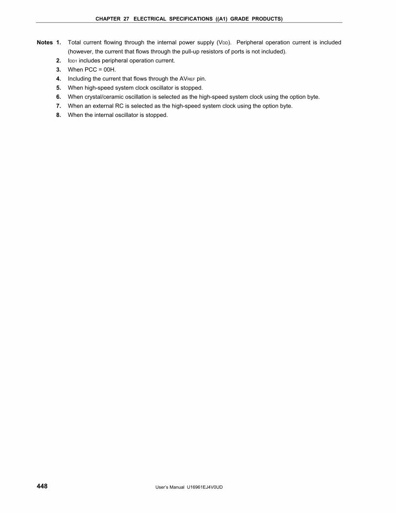
CHAPTER 27 ELECTRICAL SPECIFICATIONS ((A1) GRADE PRODUCTS)
User’s Manual U16961EJ4V0UD 448
Notes 1. Total current flowing through the internal power supply (VDD). Peripheral operation current is included (however, the current that flows through the pull-up resistors of ports is not included).
2. IDD1 includes peripheral operation current. 3. When PCC = 00H. 4. Including the current that flows through the AVREF pin. 5. When high-speed system clock oscillator is stopped. 6. When crystal/ceramic oscillation is selected as the high-speed system clock using the option byte. 7. When an external RC is selected as the high-speed system clock using the option byte. 8. When the internal oscillator is stopped.
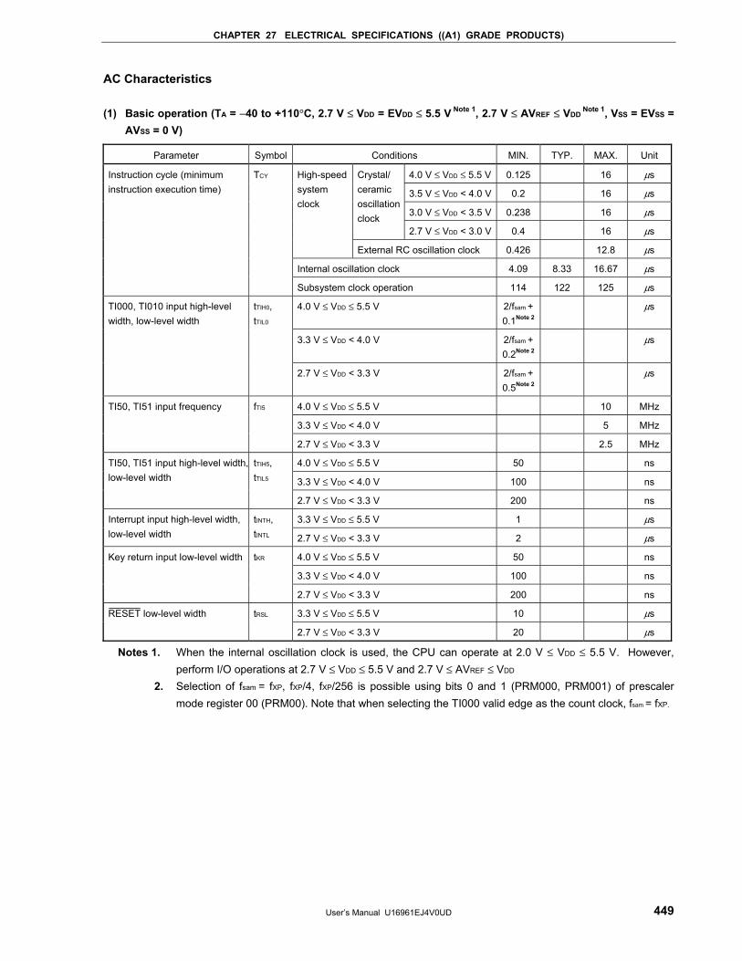
CHAPTER 27 ELECTRICAL SPECIFICATIONS ((A1) GRADE PRODUCTS)
User’s Manual U16961EJ4V0UD 449
AC Characteristics (1) Basic operation (TA = −40 to +110°C, 2.7 V ≤ VDD = EVDD ≤ 5.5 V Note 1, 2.7 V ≤ AVREF ≤ VDD
Note 1, VSS = EVSS = AVSS = 0 V)
Parameter Symbol Conditions MIN. TYP. MAX. Unit
4.0 V ≤ VDD ≤ 5.5 V 0.125 16 μs
3.5 V ≤ VDD < 4.0 V 0.2 16 μs
3.0 V ≤ VDD < 3.5 V 0.238 16 μs
Crystal/ ceramic oscillation clock
2.7 V ≤ VDD < 3.0 V 0.4 16 μs
High-speed system clock
External RC oscillation clock 0.426 12.8 μs
Internal oscillation clock 4.09 8.33 16.67 μs
Instruction cycle (minimum instruction execution time)
TCY
Subsystem clock operation 114 122 125 μs
4.0 V ≤ VDD ≤ 5.5 V 2/fsam + 0.1Note 2
μs
3.3 V ≤ VDD < 4.0 V 2/fsam + 0.2Note 2
μs
TI000, TI010 input high-level width, low-level width
tTIH0, tTIL0
2.7 V ≤ VDD < 3.3 V 2/fsam + 0.5Note 2
μs
4.0 V ≤ VDD ≤ 5.5 V 10 MHz
3.3 V ≤ VDD < 4.0 V 5 MHz
TI50, TI51 input frequency fTI5
2.7 V ≤ VDD < 3.3 V 2.5 MHz
4.0 V ≤ VDD ≤ 5.5 V 50 ns
3.3 V ≤ VDD < 4.0 V 100 ns
TI50, TI51 input high-level width, low-level width
tTIH5, tTIL5
2.7 V ≤ VDD < 3.3 V 200 ns
3.3 V ≤ VDD ≤ 5.5 V 1 μs Interrupt input high-level width, low-level width
tINTH, tINTL 2.7 V ≤ VDD < 3.3 V 2 μs
4.0 V ≤ VDD ≤ 5.5 V 50 ns
3.3 V ≤ VDD < 4.0 V 100 ns
Key return input low-level width tKR
2.7 V ≤ VDD < 3.3 V 200 ns
3.3 V ≤ VDD ≤ 5.5 V 10 μs RESET low-level width tRSL
2.7 V ≤ VDD < 3.3 V 20 μs
Notes 1. When the internal oscillation clock is used, the CPU can operate at 2.0 V ≤ VDD ≤ 5.5 V. However, perform I/O operations at 2.7 V ≤ VDD ≤ 5.5 V and 2.7 V ≤ AVREF ≤ VDD
2. Selection of fsam = fXP, fXP/4, fXP/256 is possible using bits 0 and 1 (PRM000, PRM001) of prescaler mode register 00 (PRM00). Note that when selecting the TI000 valid edge as the count clock, fsam = fXP.
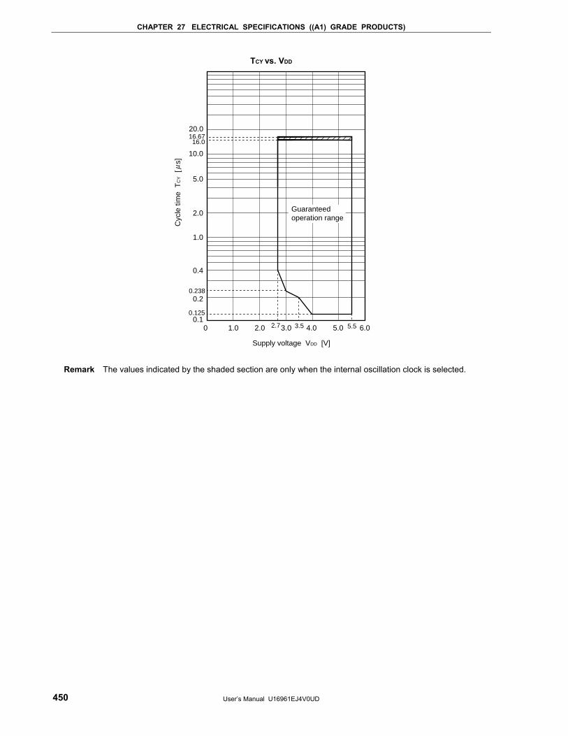
CHAPTER 27 ELECTRICAL SPECIFICATIONS ((A1) GRADE PRODUCTS)
User’s Manual U16961EJ4V0UD 450
TCY vs. VDD
5.0
1.0
2.0
0.4
0.2
0.10
10.0
1.0 2.0 3.0 4.0 5.0 6.05.5
20.0
16.0
0.238
0.125
3.52.7
16.67
Supply voltage VDD [V]
Guaranteed operation range
Cyc
le ti
me
TC
Y [
s]
μ
Remark The values indicated by the shaded section are only when the internal oscillation clock is selected.
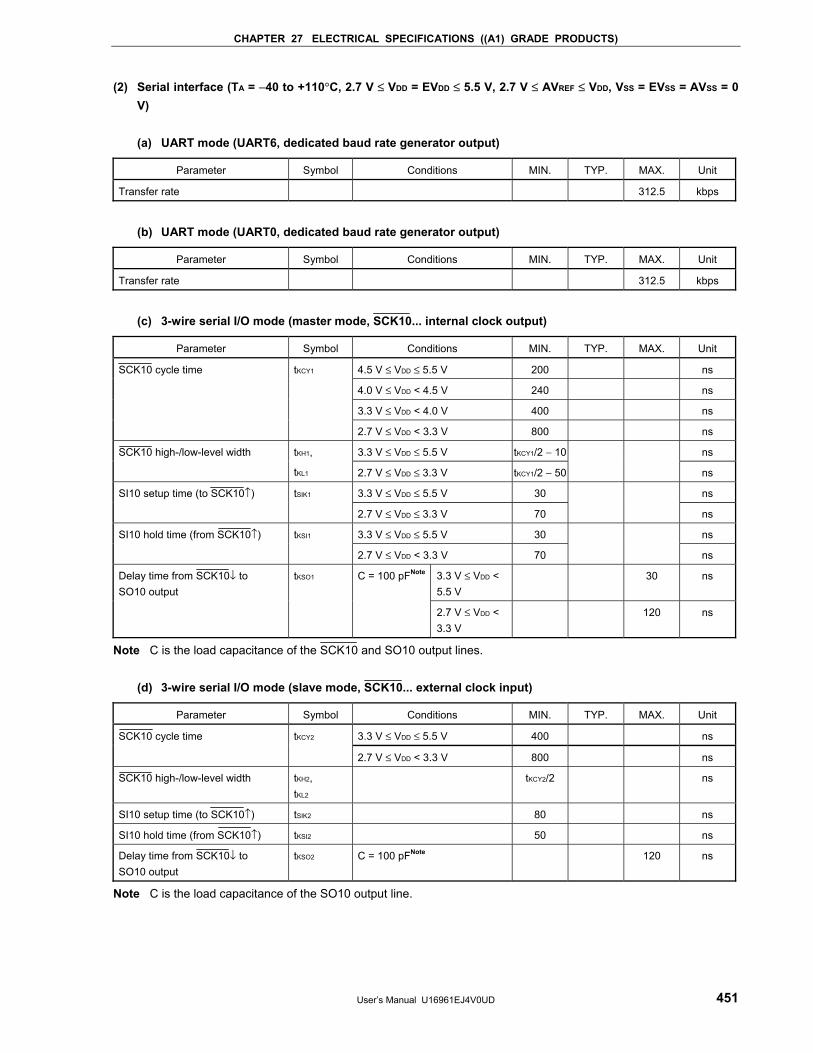
CHAPTER 27 ELECTRICAL SPECIFICATIONS ((A1) GRADE PRODUCTS)
User’s Manual U16961EJ4V0UD 451
(2) Serial interface (TA = −40 to +110°C, 2.7 V ≤ VDD = EVDD ≤ 5.5 V, 2.7 V ≤ AVREF ≤ VDD, VSS = EVSS = AVSS = 0 V)
(a) UART mode (UART6, dedicated baud rate generator output)
Parameter Symbol Conditions MIN. TYP. MAX. Unit
Transfer rate 312.5 kbps
(b) UART mode (UART0, dedicated baud rate generator output)
Parameter Symbol Conditions MIN. TYP. MAX. Unit
Transfer rate 312.5 kbps
(c) 3-wire serial I/O mode (master mode, SCK10... internal clock output)
Parameter Symbol Conditions MIN. TYP. MAX. Unit
4.5 V ≤ VDD ≤ 5.5 V 200 ns
4.0 V ≤ VDD < 4.5 V 240 ns
3.3 V ≤ VDD < 4.0 V 400 ns
SCK10 cycle time tKCY1
2.7 V ≤ VDD < 3.3 V 800 ns
3.3 V ≤ VDD ≤ 5.5 V tKCY1/2 − 10 ns SCK10 high-/low-level width tKH1,
tKL1 2.7 V ≤ VDD ≤ 3.3 V tKCY1/2 − 50
ns
3.3 V ≤ VDD ≤ 5.5 V 30 ns SI10 setup time (to SCK10↑) tSIK1
2.7 V ≤ VDD ≤ 3.3 V 70
ns
3.3 V ≤ VDD ≤ 5.5 V 30 ns SI10 hold time (from SCK10↑) tKSI1
2.7 V ≤ VDD < 3.3 V 70
ns
3.3 V ≤ VDD < 5.5 V
30 ns Delay time from SCK10↓ to SO10 output
tKSO1 C = 100 pFNote
2.7 V ≤ VDD < 3.3 V
120 ns
Note C is the load capacitance of the SCK10 and SO10 output lines.
(d) 3-wire serial I/O mode (slave mode, SCK10... external clock input)
Parameter Symbol Conditions MIN. TYP. MAX. Unit
3.3 V ≤ VDD ≤ 5.5 V 400 ns SCK10 cycle time tKCY2
2.7 V ≤ VDD < 3.3 V 800 ns
SCK10 high-/low-level width tKH2, tKL2
tKCY2/2 ns
SI10 setup time (to SCK10↑) tSIK2 80 ns
SI10 hold time (from SCK10↑) tKSI2 50 ns
Delay time from SCK10↓ to SO10 output
tKSO2 C = 100 pFNote 120 ns
Note C is the load capacitance of the SO10 output line.
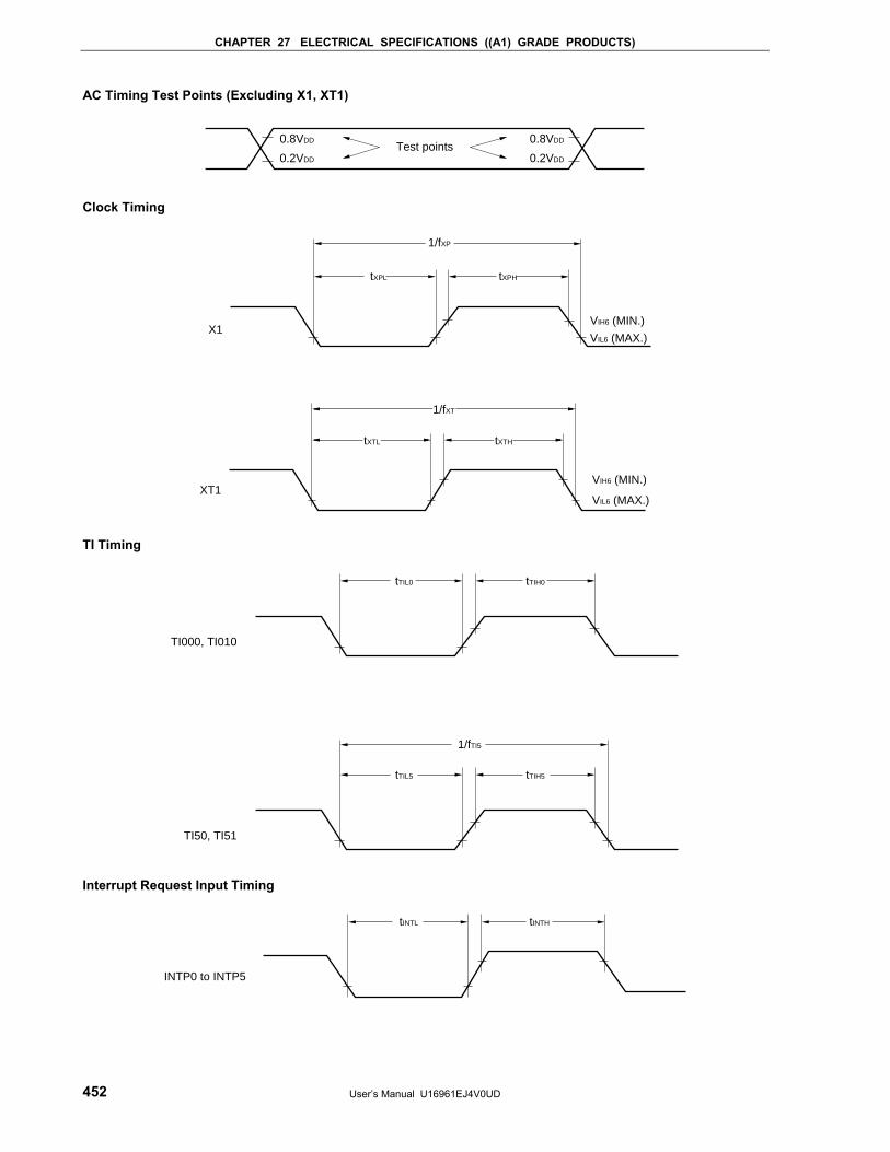
CHAPTER 27 ELECTRICAL SPECIFICATIONS ((A1) GRADE PRODUCTS)
User’s Manual U16961EJ4V0UD 452
AC Timing Test Points (Excluding X1, XT1)
0.8VDD
0.2VDD
Test points0.8VDD
0.2VDD
Clock Timing
X1VIH6 (MIN.)
VIL6 (MAX.)
1/fXP
tXPL tXPH
1/fXT
tXTL tXTH
XT1VIH6 (MIN.)
VIL6 (MAX.) TI Timing
TI000, TI010
tTIL0 tTIH0
TI50, TI51
1/fTI5
tTIL5 tTIH5
Interrupt Request Input Timing
INTP0 to INTP5
tINTL tINTH
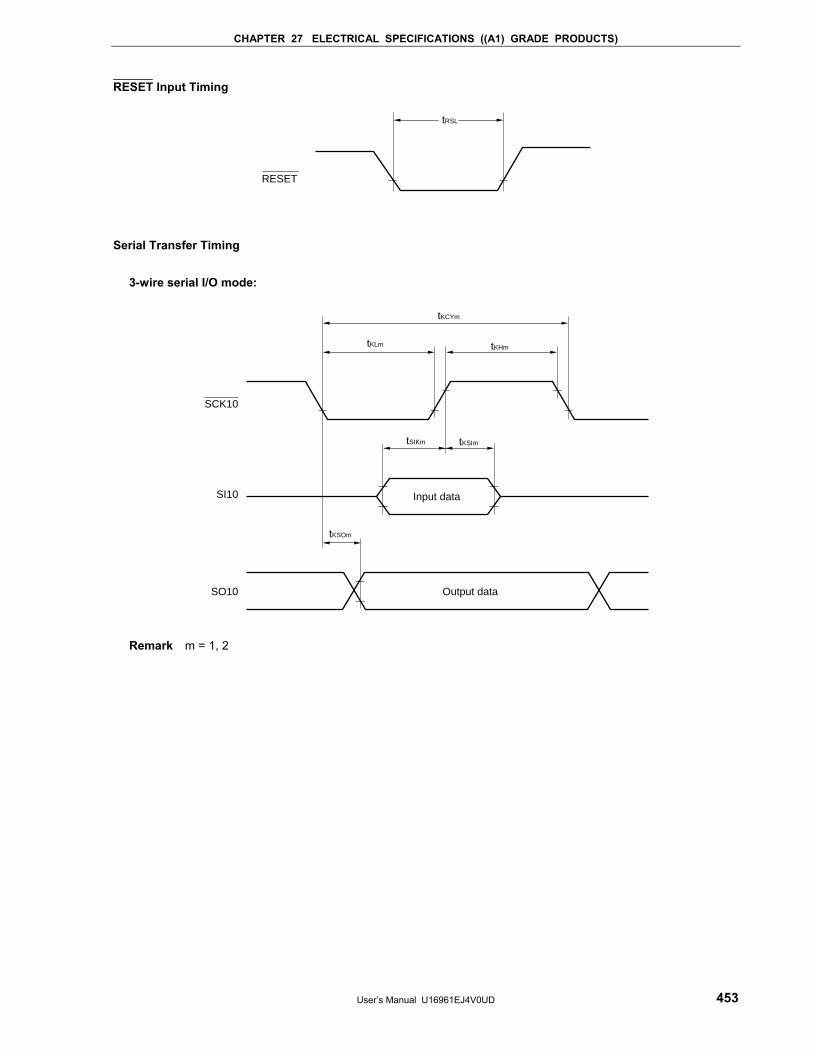
CHAPTER 27 ELECTRICAL SPECIFICATIONS ((A1) GRADE PRODUCTS)
User’s Manual U16961EJ4V0UD 453
RESET Input Timing
RESET
tRSL
Serial Transfer Timing
3-wire serial I/O mode:
SI10
SO10
tKCYm
tKLm tKHm
tSIKm tKSIm
Input data
tKSOm
Output data
SCK10
Remark m = 1, 2
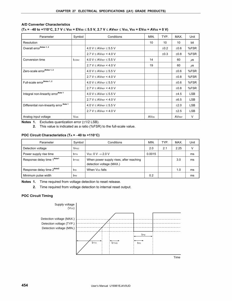
CHAPTER 27 ELECTRICAL SPECIFICATIONS ((A1) GRADE PRODUCTS)
User’s Manual U16961EJ4V0UD 454
A/D Converter Characteristics (TA = −40 to +110°C, 2.7 V ≤ VDD = EVDD ≤ 5.5 V, 2.7 V ≤ AVREF ≤ VDD, VSS = EVSS = AVSS = 0 V)
Parameter Symbol Conditions MIN. TYP. MAX. Unit
Resolution 10 10 10 bit
4.0 V ≤ AVREF ≤ 5.5 V ±0.2 ±0.6 %FSR Overall errorNotes 1, 2
2.7 V ≤ AVREF < 4.0 V ±0.3 ±0.8 %FSR
4.0 V ≤ AVREF ≤ 5.5 V 14 60 μs Conversion time tCONV
2.7 V ≤ AVREF < 4.0 V 19 60 μs
4.0 V ≤ AVREF ≤ 5.5 V ±0.6 %FSR Zero-scale errorNotes 1, 2
2.7 V ≤ AVREF < 4.0 V ±0.8 %FSR
4.0 V ≤ AVREF ≤ 5.5 V ±0.6 %FSR Full-scale errorNotes 1, 2
2.7 V ≤ AVREF < 4.0 V ±0.8 %FSR
4.0 V ≤ AVREF ≤ 5.5 V ±4.5 LSB Integral non-linearity errorNote 1
2.7 V ≤ AVREF < 4.0 V ±6.5 LSB
4.0 V ≤ AVREF ≤ 5.5 V ±2.0 LSB Differential non-linearity error Note 1
2.7 V ≤ AVREF < 4.0 V ±2.5 LSB
Analog input voltage VAIN AVSS AVREF V
Notes 1. Excludes quantization error (±1/2 LSB). 2. This value is indicated as a ratio (%FSR) to the full-scale value. POC Circuit Characteristics (TA = −40 to +110°C)
Parameter Symbol Conditions MIN. TYP. MAX. Unit
Detection voltage VPOC 2.0 2.1 2.25 V
Power supply rise time tPTH VDD: 0 V → 2.0 V 0.0015 ms
Response delay time 1Note1 tPTHD When power supply rises, after reaching detection voltage (MAX.)
3.0 ms
Response delay time 2Note2 tPD When VDD falls 1.0 ms
Minimum pulse width tPW 0.2 ms
Notes 1. Time required from voltage detection to reset release. 2. Time required from voltage detection to internal reset output. POC Circuit Timing
Supply voltage(VDD)
Time
Detection voltage (MIN.)
Detection voltage (TYP.)
Detection voltage (MAX.)
tPTH tPTHD
tPW
tPD
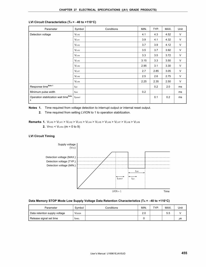
CHAPTER 27 ELECTRICAL SPECIFICATIONS ((A1) GRADE PRODUCTS)
User’s Manual U16961EJ4V0UD 455
LVI Circuit Characteristics (TA = −40 to +110°C)
Parameter Symbol Conditions MIN. TYP. MAX. Unit
VLVI0 4.1 4.3 4.52 V
VLVI1 3.9 4.1 4.32 V
VLVI2 3.7 3.9 4.12 V
VLVI3 3.5 3.7 3.92 V
VLVI4 3.3 3.5 3.72 V
VLVI5 3.15 3.3 3.50 V
VLVI6 2.95 3.1 3.30 V
VLVI7 2.7 2.85 3.05 V
VLVI8 2.5 2.6 2.75 V
Detection voltage
VLVI9 2.25 2.35 2.50 V
Response timeNote 1 tLD 0.2 2.0 ms
Minimum pulse width tLW 0.2 ms
Operation stabilization wait timeNote
2 tLWAIT 0.1 0.2 ms
Notes 1. Time required from voltage detection to interrupt output or internal reset output. 2. Time required from setting LVION to 1 to operation stabilization. Remarks 1. VLVI0 > VLVI1 > VLVI2 > VLVI3 > VLVI4 > VLVI5 > VLVI6 > VLVI7 > VLVI8 > VLVI9 2. VPOC < VLVIm (m = 0 to 9) LVI Circuit Timing
Supply voltage(VDD)
Time
Detection voltage (MIN.)
Detection voltage (TYP.)
Detection voltage (MAX.)
tLW
tLDtLWAIT
LVION ← 1 Data Memory STOP Mode Low Supply Voltage Data Retention Characteristics (TA = −40 to +110°C)
Parameter Symbol Conditions MIN. TYP. MAX. Unit
Data retention supply voltage VDDDR 2.0 5.5 V
Release signal set time tSREL 0 μs
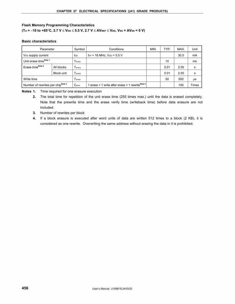
CHAPTER 27 ELECTRICAL SPECIFICATIONS ((A1) GRADE PRODUCTS)
User’s Manual U16961EJ4V0UD 456
Flash Memory Programming Characteristics (TA = −10 to +65°C, 2.7 V ≤ VDD ≤ 5.5 V, 2.7 V ≤ AVREF ≤ VDD, VSS = AVSS = 0 V) Basic characteristics
Parameter Symbol Conditions MIN. TYP. MAX. Unit
VDD supply current IDD fXP = 16 MHz, VDD = 5.5 V 30.5 mA
Unit erase timeNote 1 Terass 10 ms
All blocks Teraca 0.01 2.55 s Erase timeNote 2
Block unit Terasa 0.01 2.55 s
Write time Twrwa 50 500 μs
Number of rewrites per chipNote 3 Cerwr 1 erase + 1 write after erase = 1 rewriteNote 4 100 Times
Notes 1. Time required for one erasure execution 2. The total time for repetition of the unit erase time (255 times max.) until the data is erased completely.
Note that the prewrite time and the erase verify time (writeback time) before data erasure are not included.
3. Number of rewrites per block 4. If a block erasure is executed after word units of data are written 512 times to a block (2 KB), it is
considered as one rewrite. Overwriting the same address without erasing the data in it is prohibited.
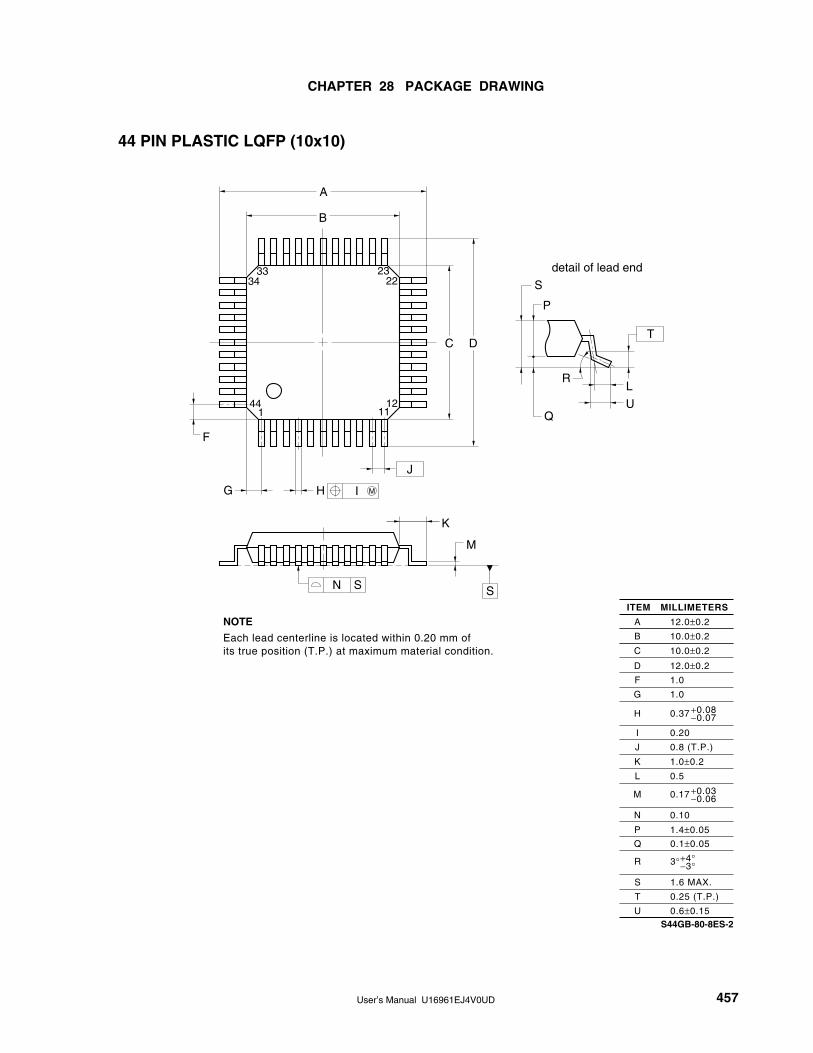
User’s Manual U16961EJ4V0UD 457
CHAPTER 28 PACKAGE DRAWING
3334 22
441
1211
23
44 PIN PLASTIC LQFP (10x10)
ITEM MILLIMETERS
N
Q 0.1±0.05
0.10
S44GB-80-8ES-2
J
IH
N
A 12.0±0.2
B 10.0±0.2
C 10.0±0.2
D 12.0±0.2
F
G
H
1.0
0.37
1.0
I
J
K
0.8 (T.P.)
1.0±0.2
0.20
L 0.5
M 0.17
S
T
U
1.6 MAX.
0.25 (T.P.)
0.6±0.15
R 3°
+0.08−0.07
+0.03−0.06
+4°−3°
detail of lead end
F
G
K
M
M
P 1.4±0.05
NOTE
S S
A
B
C D
U
R
S
P
Q
L
T
Each lead centerline is located within 0.20 mm ofits true position (T.P.) at maximum material condition.
User’s Manual U16961EJ4V0UD 458
CHAPTER 29 RECOMMENDED SOLDERING CONDITIONS
These products should be soldered and mounted under the following recommended conditions.
For technical information, see the following website.
Semiconductor Device Mount Manual (http://www.necel.com/pkg/en/mount/index.html)
Table 29-1. Surface Mounting Type Soldering Conditions
(1) µPD78F0112HGB-8ES, 78F0113HGB-8ES, 78F0114HGB-8ES
µPD78F0112HGB(A)-8ES, 78F0113HGB(A)-8ES, 78F0114HGB(A)-8ES
µPD78F0112HGB(A1)-8ES, 78F0113HGB(A1)-8ES, 78F0114HGB(A1)-8ES
Soldering Method Soldering Conditions Recommended
Condition Symbol
Infrared reflow Package peak temperature: 235°C, Time: 30 seconds max. (at 210°C or higher),
Count: 3 times or less, Exposure limit: 7 daysNote (after that, prebake at 125°C for
20 to 72 hours)
IR35-207-3
VPS Package peak temperature: 215°C, Time: 40 seconds max. (at 200°C or higher),
Count: 3 times or less, Exposure limit: 7 daysNote (after that, prebake at 125°C for
20 to 72 hours)
VP15-207-3
Wave soldering Solder bath temperature: 260°C max., Time: 10 seconds max., Count: Once,
Preheating temperature: 120°C max. (package surface temperature), Exposure
limit: 7 daysNote (after that, prebake at 125°C for 20 to 72 hours)
WS60-207-1
Partial heating Pin temperature: 350°C max., Time: 3 seconds max. (per pin row) −
Note After opening the dry pack, store it at 25°C or less and 65% RH or less for the allowable storage period.
(2) µPD78F0112HGB-8ES-A, 78F0113HGB-8ES-A, 78F0114HGB-8ES-A
µPD78F0112HGB(A)-8ES-A, 78F0113HGB(A)-8ES-A, 78F0114HGB(A)-8ES-A
µPD78F0112HGB(A1)-8ES-A, 78F0113HGB(A1)-8ES-A, 78F0114HGB(A1)-8ES-A
Soldering Method Soldering Conditions Recommended
Condition Symbol
Infrared reflow Package peak temperature: 260°C, Time: 60 seconds max. (at 220°C or higher),
Count: Three times or less, Exposure limit: 7 daysNote (after that, prebake at 125°C
for 20 to 72 hours)
IR60-207-3
Partial heating Pin temperature: 350°C max., Time: 3 seconds max. (per pin row) −
Note After opening the dry pack, store it at 25°C or less and 65% RH or less for the allowable storage period.
Caution Do not use different soldering methods together (except for partial heating).
Remarks Products that have the part numbers suffixed by "-A" are lead-free products.
<R>
User’s Manual U16961EJ4V0UD 459
CHAPTER 30 CAUTIONS FOR WAIT
30.1 Cautions for Wait
This product has two internal system buses.
One is a CPU bus and the other is a peripheral bus that interfaces with the low-speed peripheral hardware.
Because the clock of the CPU bus and the clock of the peripheral bus are asynchronous, unexpected illegal data
may be passed if an access to the CPU conflicts with an access to the peripheral hardware.
When accessing the peripheral hardware that may cause a conflict, therefore, the CPU repeatedly executes
processing, until the correct data is passed.
As a result, the CPU does not start the next instruction processing but waits. If this happens, the number of
execution clocks of an instruction increases by the number of wait clocks (for the number of wait clocks, refer to Table
30-1). This must be noted when real-time processing is performed.
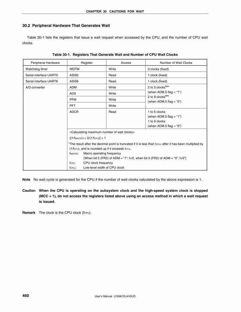
CHAPTER 30 CAUTIONS FOR WAIT
User’s Manual U16961EJ4V0UD 460
30.2 Peripheral Hardware That Generates Wait
Table 30-1 lists the registers that issue a wait request when accessed by the CPU, and the number of CPU wait
clocks.
Table 30-1. Registers That Generate Wait and Number of CPU Wait Clocks
Peripheral Hardware Register Access Number of Wait Clocks
Watchdog timer WDTM Write 3 clocks (fixed)
Serial interface UART0 ASIS0 Read 1 clock (fixed)
Serial interface UART6 ASIS6 Read 1 clock (fixed)
ADM Write
ADS Write
PFM Write
PFT Write
2 to 5 clocksNote
(when ADM.5 flag = “1”)
2 to 9 clocksNote
(when ADM.5 flag = “0”)
ADCR Read 1 to 5 clocks
(when ADM.5 flag = “1”)
1 to 9 clocks
(when ADM.5 flag = “0”)
A/D converter
<Calculating maximum number of wait clocks>
(1/fMACRO) × 2/(1/fCPU) + 1
*The result after the decimal point is truncated if it is less than tCPUL after it has been multiplied by
(1/fCPU), and is rounded up if it exceeds tCPUL.
fMACRO: Macro operating frequency
(When bit 5 (FR2) of ADM = “1”: fX/2, when bit 5 (FR2) of ADM = “0”: fX/22)
fCPU: CPU clock frequency
tCPUL: Low-level width of CPU clock
Note No wait cycle is generated for the CPU if the number of wait clocks calculated by the above expression is 1.
Caution When the CPU is operating on the subsystem clock and the high-speed system clock is stopped
(MCC = 1), do not access the registers listed above using an access method in which a wait request
is issued.
Remark The clock is the CPU clock (fCPU).
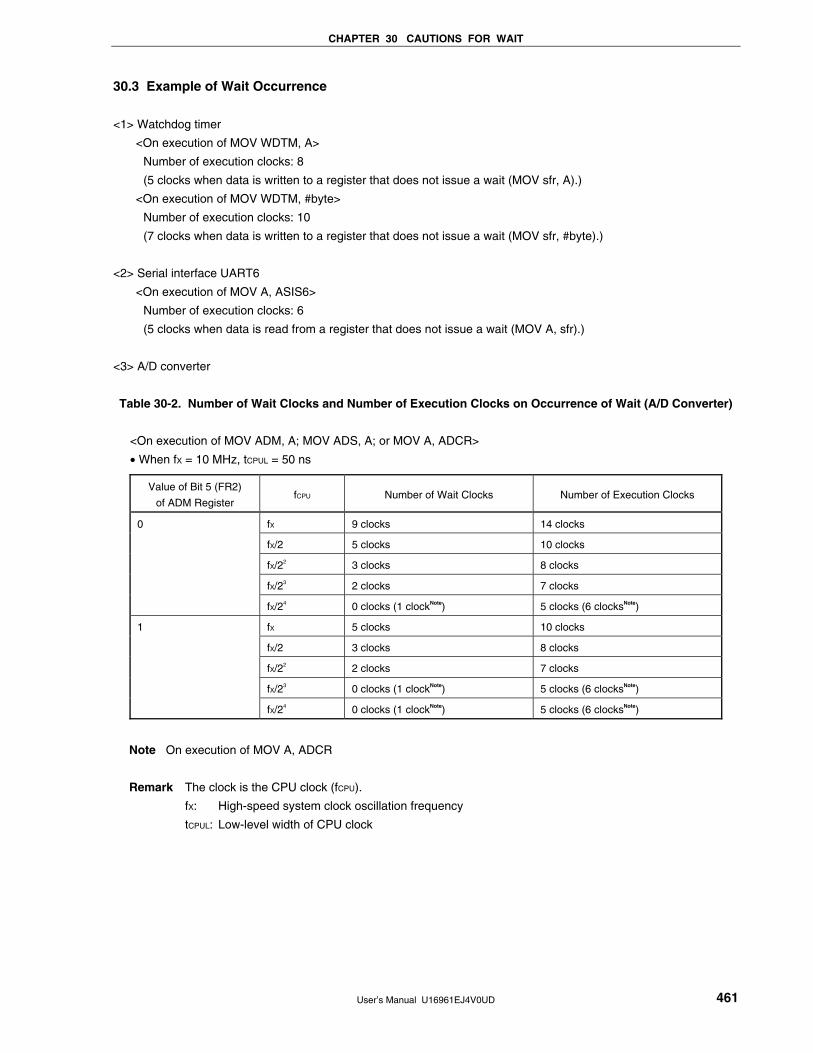
CHAPTER 30 CAUTIONS FOR WAIT
User’s Manual U16961EJ4V0UD 461
30.3 Example of Wait Occurrence
<1> Watchdog timer
<On execution of MOV WDTM, A>
Number of execution clocks: 8
(5 clocks when data is written to a register that does not issue a wait (MOV sfr, A).)
<On execution of MOV WDTM, #byte>
Number of execution clocks: 10
(7 clocks when data is written to a register that does not issue a wait (MOV sfr, #byte).)
<2> Serial interface UART6
<On execution of MOV A, ASIS6>
Number of execution clocks: 6
(5 clocks when data is read from a register that does not issue a wait (MOV A, sfr).)
<3> A/D converter
Table 30-2. Number of Wait Clocks and Number of Execution Clocks on Occurrence of Wait (A/D Converter)
<On execution of MOV ADM, A; MOV ADS, A; or MOV A, ADCR>
• When fX = 10 MHz, tCPUL = 50 ns
Value of Bit 5 (FR2)
of ADM Register fCPU Number of Wait Clocks Number of Execution Clocks
fX 9 clocks 14 clocks
fX/2 5 clocks 10 clocks
fX/22 3 clocks 8 clocks
fX/23 2 clocks 7 clocks
0
fX/24 0 clocks (1 clockNote) 5 clocks (6 clocksNote)
fX 5 clocks 10 clocks
fX/2 3 clocks 8 clocks
fX/22 2 clocks 7 clocks
fX/23 0 clocks (1 clockNote) 5 clocks (6 clocksNote)
1
fX/24 0 clocks (1 clockNote) 5 clocks (6 clocksNote)
Note On execution of MOV A, ADCR
Remark The clock is the CPU clock (fCPU).
fX: High-speed system clock oscillation frequency
tCPUL: Low-level width of CPU clock
User’s Manual U16961EJ4V0UD 462
APPENDIX A DEVELOPMENT TOOLS
The following development tools are available for the development of systems that employ the 78K0/KC1+.
Figure A-1 shows the development tool configuration.
• Support for PC98-NX series
Unless otherwise specified, products supported by IBM PC/ATTM compatibles are compatible with PC98-NX
series computers. When using PC98-NX series computers, refer to the explanation for IBM PC/AT compatibles.
• WindowsTM
Unless otherwise specified, “Windows” means the following OSs.
• Windows 3.1
• Windows 95
• Windows 98
• Windows NTTM Ver 4.0
• Windows 2000
• Windows XPTM
Caution For the development tools of the 78K0/KC1+, contact an NEC Electronics sales representative.
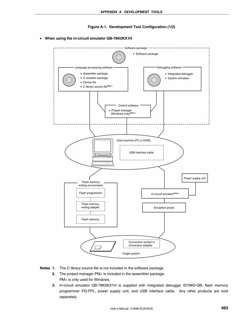
APPENDIX A DEVELOPMENT TOOLS
User’s Manual U16961EJ4V0UD 463
Figure A-1. Development Tool Configuration (1/2)
• When using the in-circuit emulator QB-78K0KX1H
In-circuit emulatorNote 3
Emulation probe
Power supply unit
Language processing software
• Assembler package
• C compiler package
• Device file
• C library source fileNote 1
Debugging software
• Integrated debugger
• System simulator
Host machine (PC or EWS)
USB interface cable
Conversion socket orconversion adapter
Target system
Flash programmer
Flash memorywriting adapter
Flash memory
• Software package
• Project manager (Windows only)Note 2
Software package
Flash memorywriting environment
Control software
Notes 1. The C library source file is not included in the software package.
2. The project manager PM+ is included in the assembler package.
PM+ is only used for Windows.
3. In-circuit emulator QB-78K0KX1H is supplied with integrated debugger ID78K0-QB, flash memory
programmer PG-FPL, power supply unit, and USB interface cable. Any other products are sold
separately.
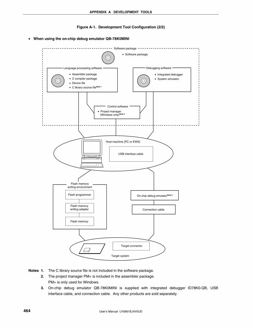
APPENDIX A DEVELOPMENT TOOLS
User’s Manual U16961EJ4V0UD 464
Figure A-1. Development Tool Configuration (2/2)
• When using the on-chip debug emulator QB-78K0MINI
On-chip debug emulatorNote 3
Connection cable
Language processing software
• Assembler package
• C compiler package
• Device file
• C library source fileNote 1
Debugging software
• Integrated debugger
• System simulator
Host machine (PC or EWS)
USB interface cable
Target connector
Target system
Flash programmer
Flash memorywriting adapter
Flash memory
• Software package
• Project manager (Windows only)Note 2
Software package
Flash memorywriting environment
Control software
Notes 1. The C library source file is not included in the software package.
2. The project manager PM+ is included in the assembler package.
PM+ is only used for Windows.
3. On-chip debug emulator QB-78K0MINI is supplied with integrated debugger ID78K0-QB, USB
interface cable, and connection cable. Any other products are sold separately.
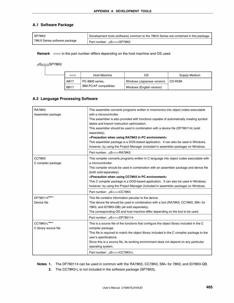
APPENDIX A DEVELOPMENT TOOLS
User’s Manual U16961EJ4V0UD 465
A.1 Software Package
Development tools (software) common to the 78K/0 Series are combined in this package.SP78K0
78K/0 Series software package Part number: µS××××SP78K0
Remark ×××× in the part number differs depending on the host machine and OS used.
µS××××SP78K0
×××× Host Machine OS Supply Medium
AB17 Windows (Japanese version)
BB17
PC-9800 series,
IBM PC/AT compatibles Windows (English version)
CD-ROM
A.2 Language Processing Software
This assembler converts programs written in mnemonics into object codes executable
with a microcontroller.
This assembler is also provided with functions capable of automatically creating symbol
tables and branch instruction optimization.
This assembler should be used in combination with a device file (DF780114) (sold
separately).
<Precaution when using RA78K0 in PC environment>
This assembler package is a DOS-based application. It can also be used in Windows,
however, by using the Project Manager (included in assembler package) on Windows.
RA78K0
Assembler package
Part number: µS××××RA78K0
This compiler converts programs written in C language into object codes executable with
a microcontroller.
This compiler should be used in combination with an assembler package and device file
(both sold separately).
<Precaution when using CC78K0 in PC environment>
This C compiler package is a DOS-based application. It can also be used in Windows,
however, by using the Project Manager (included in assembler package) on Windows.
CC78K0
C compiler package
Part number: µS××××CC78K0
This file contains information peculiar to the device.
This device file should be used in combination with a tool (RA78K0, CC78K0, SM+ for
78K0, and ID78K0-QB) (all sold separately).
The corresponding OS and host machine differ depending on the tool to be used.
DF780114Notes 1
Device file
Part number: µS××××DF780114
This is a source file of the functions that configure the object library included in the C
compiler package.
This file is required to match the object library included in the C compiler package to the
user’s specifications.
Since this is a source file, its working environment does not depend on any particular
operating system.
CC78K0-LNote 2
C library source file
Part number: µS××××CC78K0-L
Notes 1. The DF780114 can be used in common with the RA78K0, CC78K0, SM+ for 78K0, and ID78K0-QB.
2. The CC78K0-L is not included in the software package (SP78K0).
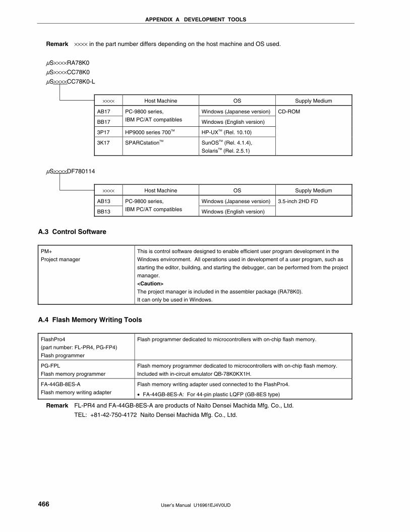
APPENDIX A DEVELOPMENT TOOLS
User’s Manual U16961EJ4V0UD 466
Remark ×××× in the part number differs depending on the host machine and OS used.
µS××××RA78K0
µS××××CC78K0
µS××××CC78K0-L
×××× Host Machine OS Supply Medium
AB17 Windows (Japanese version)
BB17
PC-9800 series,
IBM PC/AT compatibles Windows (English version)
3P17 HP9000 series 700TM HP-UXTM (Rel. 10.10)
3K17 SPARCstationTM SunOSTM (Rel. 4.1.4),
SolarisTM (Rel. 2.5.1)
CD-ROM
µS××××DF780114
×××× Host Machine OS Supply Medium
AB13 Windows (Japanese version)
BB13
PC-9800 series,
IBM PC/AT compatibles Windows (English version)
3.5-inch 2HD FD
A.3 Control Software
PM+
Project manager
This is control software designed to enable efficient user program development in the
Windows environment. All operations used in development of a user program, such as
starting the editor, building, and starting the debugger, can be performed from the project
manager.
<Caution>
The project manager is included in the assembler package (RA78K0).
It can only be used in Windows.
A.4 Flash Memory Writing Tools
FlashPro4
(part number: FL-PR4, PG-FP4)
Flash programmer
Flash programmer dedicated to microcontrollers with on-chip flash memory.
PG-FPL
Flash memory programmer
Flash memory programmer dedicated to microcontrollers with on-chip flash memory.
Included with in-circuit emulator QB-78K0KX1H.
FA-44GB-8ES-A
Flash memory writing adapter
Flash memory writing adapter used connected to the FlashPro4.
• FA-44GB-8ES-A: For 44-pin plastic LQFP (GB-8ES type)
Remark FL-PR4 and FA-44GB-8ES-A are products of Naito Densei Machida Mfg. Co., Ltd.
TEL: +81-42-750-4172 Naito Densei Machida Mfg. Co., Ltd.
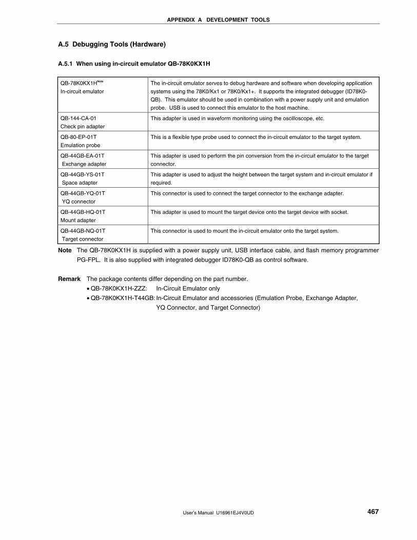
APPENDIX A DEVELOPMENT TOOLS
User’s Manual U16961EJ4V0UD 467
A.5 Debugging Tools (Hardware)
A.5.1 When using in-circuit emulator QB-78K0KX1H
QB-78K0KX1HNote
In-circuit emulator
The in-circuit emulator serves to debug hardware and software when developing application
systems using the 78K0/Kx1 or 78K0/Kx1+. It supports the integrated debugger (ID78K0-
QB). This emulator should be used in combination with a power supply unit and emulation
probe. USB is used to connect this emulator to the host machine.
QB-144-CA-01
Check pin adapter
This adapter is used in waveform monitoring using the oscilloscope, etc.
QB-80-EP-01T
Emulation probe
This is a flexible type probe used to connect the in-circuit emulator to the target system.
QB-44GB-EA-01T
Exchange adapter
This adapter is used to perform the pin conversion from the in-circuit emulator to the target
connector.
QB-44GB-YS-01T
Space adapter
This adapter is used to adjust the height between the target system and in-circuit emulator if
required.
QB-44GB-YQ-01T
YQ connector
This connector is used to connect the target connector to the exchange adapter.
QB-44GB-HQ-01T
Mount adapter
This adapter is used to mount the target device onto the target device with socket.
QB-44GB-NQ-01T
Target connector
This connector is used to mount the in-circuit emulator onto the target system.
Note The QB-78K0KX1H is supplied with a power supply unit, USB interface cable, and flash memory programmer
PG-FPL. It is also supplied with integrated debugger ID78K0-QB as control software.
Remark The package contents differ depending on the part number.
• QB-78K0KX1H-ZZZ: In-Circuit Emulator only
• QB-78K0KX1H-T44GB: In-Circuit Emulator and accessories (Emulation Probe, Exchange Adapter,
YQ Connector, and Target Connector)
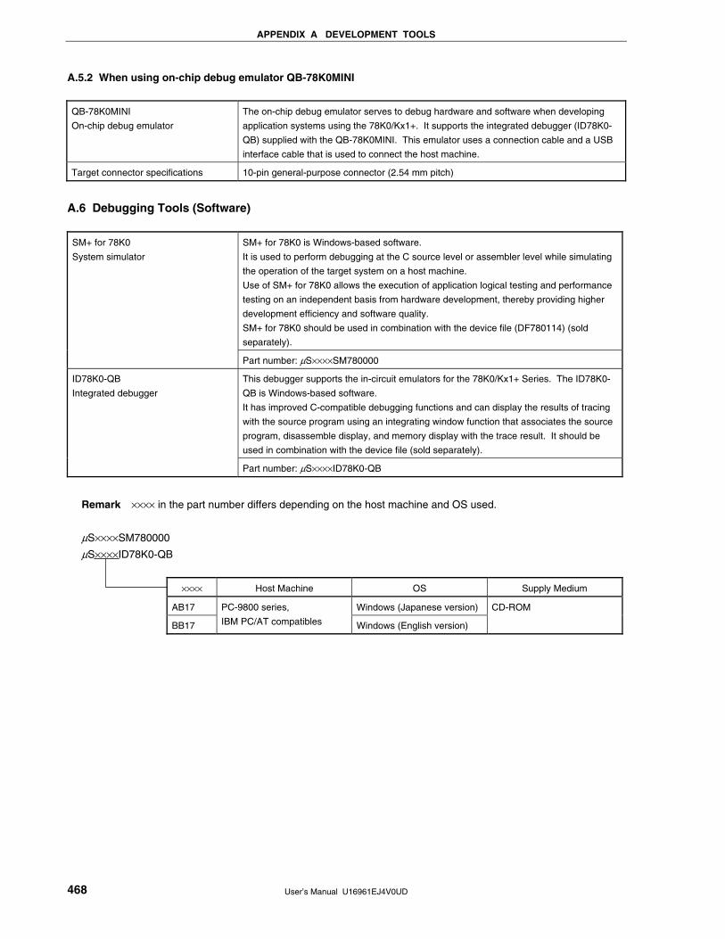
APPENDIX A DEVELOPMENT TOOLS
User’s Manual U16961EJ4V0UD 468
A.5.2 When using on-chip debug emulator QB-78K0MINI
QB-78K0MINI
On-chip debug emulator
The on-chip debug emulator serves to debug hardware and software when developing
application systems using the 78K0/Kx1+. It supports the integrated debugger (ID78K0-
QB) supplied with the QB-78K0MINI. This emulator uses a connection cable and a USB
interface cable that is used to connect the host machine.
Target connector specifications 10-pin general-purpose connector (2.54 mm pitch)
A.6 Debugging Tools (Software)
SM+ for 78K0 is Windows-based software.
It is used to perform debugging at the C source level or assembler level while simulating
the operation of the target system on a host machine.
Use of SM+ for 78K0 allows the execution of application logical testing and performance
testing on an independent basis from hardware development, thereby providing higher
development efficiency and software quality.
SM+ for 78K0 should be used in combination with the device file (DF780114) (sold
separately).
SM+ for 78K0
System simulator
Part number: µS××××SM780000
This debugger supports the in-circuit emulators for the 78K0/Kx1+ Series. The ID78K0-
QB is Windows-based software.
It has improved C-compatible debugging functions and can display the results of tracing
with the source program using an integrating window function that associates the source
program, disassemble display, and memory display with the trace result. It should be
used in combination with the device file (sold separately).
ID78K0-QB
Integrated debugger
Part number: µS××××ID78K0-QB
Remark ×××× in the part number differs depending on the host machine and OS used.
µS××××SM780000
µS××××ID78K0-QB
×××× Host Machine OS Supply Medium
AB17 Windows (Japanese version)
BB17
PC-9800 series,
IBM PC/AT compatibles Windows (English version)
CD-ROM
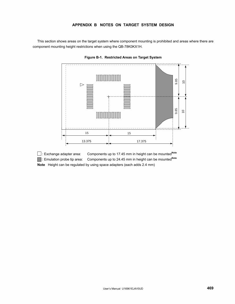
User’s Manual U16961EJ4V0UD 469
APPENDIX B NOTES ON TARGET SYSTEM DESIGN This section shows areas on the target system where component mounting is prohibited and areas where there are
component mounting height restrictions when using the QB-78K0KX1H.
Figure B-1. Restricted Areas on Target System
15
9.85
13.375
10
15
9.85
17.375
10
: Exchange adapter area: Components up to 17.45 mm in height can be mountedNote : Emulation probe tip area: Components up to 24.45 mm in height can be mountedNote Note Height can be regulated by using space adapters (each adds 2.4 mm)
User’s Manual U16961EJ4V0UD 470
APPENDIX C REGISTER INDEX
C.1 Register Index (In Alphabetical Order with Respect to Register Names)
[A]
A/D conversion result register (ADCR)........................................................................................................................228
A/D converter mode register (ADM) ............................................................................................................................225
Analog input channel specification register (ADS) ......................................................................................................227
Asynchronous serial interface control register 6 (ASICL6)..........................................................................................277
Asynchronous serial interface operation mode register 0 (ASIM0) .............................................................................247
Asynchronous serial interface operation mode register 6 (ASIM6) .............................................................................271
Asynchronous serial interface reception error status register 0 (ASIS0) .....................................................................249
Asynchronous serial interface reception error status register 6 (ASIS6) .....................................................................273
Asynchronous serial interface transmission status register 6 (ASIF6) ........................................................................274
[B]
Baud rate generator control register 0 (BRGC0) .........................................................................................................250
Baud rate generator control register 6 (BRGC6) .........................................................................................................276
[C]
Capture/compare control register 00 (CRC00)............................................................................................................132
Clock monitor mode register (CLM) ............................................................................................................................356
Clock selection register 6 (CKSR6).............................................................................................................................275
[E]
8-bit timer compare register 50 (CR50).......................................................................................................................164
8-bit timer compare register 51 (CR51).......................................................................................................................164
8-bit timer counter 50 (TM50)......................................................................................................................................163
8-bit timer counter 51 (TM51)......................................................................................................................................163
8-bit timer H carrier control register 1 (TMCYC1)........................................................................................................187
8-bit timer H compare register 00 (CMP00).................................................................................................................182
8-bit timer H compare register 01 (CMP01).................................................................................................................182
8-bit timer H compare register 10 (CMP10).................................................................................................................182
8-bit timer H compare register 11 (CMP11).................................................................................................................182
8-bit timer H mode register 0 (TMHMD0) ....................................................................................................................183
8-bit timer H mode register 1 (TMHMD1) ....................................................................................................................183
8-bit timer mode control register 50 (TMC50)..............................................................................................................167
8-bit timer mode control register 51 (TMC51)..............................................................................................................167
External interrupt falling edge enable register (EGN)..................................................................................................324
External interrupt rising edge enable register (EGP)...................................................................................................324
[F]
Flash-programming mode control register (FLPMC) ...................................................................................................399
Flash protect command register (PFCMD)..................................................................................................................401
Flash status register (PFS)..........................................................................................................................................401
APPENDIX C REGISTER INDEX
User’s Manual U16961EJ4V0UD 471
[I]
Input switch control register (ISC) ...............................................................................................................................279
Internal memory size switching register (IMS) ............................................................................................................382
Internal oscillation mode register (RCM).....................................................................................................................100
Interrupt mask flag register 0H (MK0H) ......................................................................................................................322
Interrupt mask flag register 0L (MK0L)........................................................................................................................322
Interrupt mask flag register 1L (MK1L)........................................................................................................................322
Interrupt request flag register 0H (IF0H) .....................................................................................................................321
Interrupt request flag register 0L (IF0L) ......................................................................................................................321
Interrupt request flag register 1L (IF1L) ......................................................................................................................321
[K]
Key return mode register (KRM) .................................................................................................................................334
[L]
Low-voltage detection level selection register (LVIS)..................................................................................................369
Low-voltage detection register (LVIM) ........................................................................................................................368
[M]
Main clock mode register (MCM) ................................................................................................................................101
Main OSC control register (MOC) ...............................................................................................................................102
[O]
Oscillation stabilization time counter status register (OSTC) ..............................................................................103, 337
Oscillation stabilization time select register (OSTS)............................................................................................104, 338
[P]
Port mode register 0 (PM0)...................................................................................................................................91, 136
Port mode register 1 (PM1)................................................................................................... 91, 169, 188, 251, 279, 306
Port mode register 12 (PM12).......................................................................................................................................91
Port mode register 3 (PM3)...................................................................................................................................91, 169
Port mode register 6 (PM6)...........................................................................................................................................91
Port mode register 7 (PM7)...........................................................................................................................................91
Port register 0 (P0)........................................................................................................................................................93
Port register 1 (P1)........................................................................................................................................................93
Port register 12 (P12)....................................................................................................................................................93
Port register 13 (P13)....................................................................................................................................................93
Port register 2 (P2)........................................................................................................................................................93
Port register 3 (P3)........................................................................................................................................................93
Port register 6 (P6)........................................................................................................................................................93
Port register 7 (P7)........................................................................................................................................................93
Power-fail comparison mode register (PFM)...............................................................................................................229
Power-fail comparison threshold register (PFT)..........................................................................................................229
Prescaler mode register 00 (PRM00)..........................................................................................................................134
Priority specification flag register 0H (PR0H) ..............................................................................................................323
Priority specification flag register 0L (PR0L) ...............................................................................................................323
Priority specification flag register 1L (PR1L) ...............................................................................................................323
Processor clock control register (PCC) .........................................................................................................................98
APPENDIX C REGISTER INDEX
User’s Manual U16961EJ4V0UD 472
Pull-up resistor option register 0 (PU0) ........................................................................................................................ 94
Pull-up resistor option register 1 (PU1) ........................................................................................................................ 94
Pull-up resistor option register 12 (PU12) .................................................................................................................... 94
Pull-up resistor option register 3 (PU3) ........................................................................................................................ 94
Pull-up resistor option register 7 (PU7) ........................................................................................................................ 94
[R]
Receive buffer register 0 (RXB0) ................................................................................................................................246
Receive buffer register 6 (RXB6) ................................................................................................................................270
Receive shift register 0 (RXS0) ...................................................................................................................................246
Receive shift register 6 (RXS6) ...................................................................................................................................270
Reset control flag register (RESF) ..............................................................................................................................354
[S]
Serial clock selection register 10 (CSIC10) .................................................................................................................305
Serial I/O shift register 10 (SIO10) ..............................................................................................................................303
Serial operation mode register 10 (CSIM10) ...............................................................................................................304
16-bit timer capture/compare register 000 (CR000) ....................................................................................................127
16-bit timer capture/compare register 010 (CR010) ....................................................................................................130
16-bit timer counter 00 (TM00)....................................................................................................................................127
16-bit timer mode control register 00 (TMC00)............................................................................................................130
16-bit timer output control register 00 (TOC00)...........................................................................................................132
[T]
Timer clock selection register 50 (TCL50)...................................................................................................................165
Timer clock selection register 51 (TCL51)...................................................................................................................165
Transmit buffer register 10 (SOTB10) .........................................................................................................................303
Transmit buffer register 6 (TXB6)................................................................................................................................270
Transmit shift register 0 (TXS0) ..................................................................................................................................246
Transmit shift register 6 (TXS6) ..................................................................................................................................270
[W]
Watch timer operation mode register (WTM) ..............................................................................................................207
Watchdog timer enable register (WDTE) ....................................................................................................................216
Watchdog timer mode register (WDTM)......................................................................................................................214
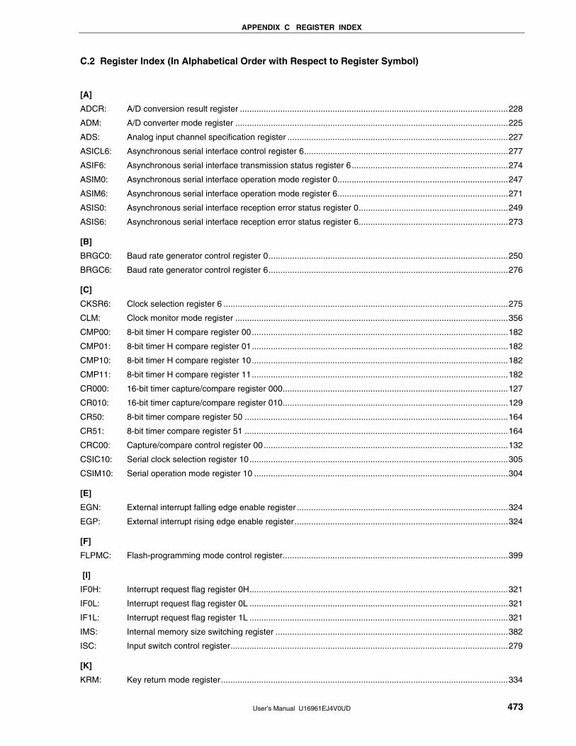
APPENDIX C REGISTER INDEX
User’s Manual U16961EJ4V0UD 473
C.2 Register Index (In Alphabetical Order with Respect to Register Symbol)
[A]
ADCR: A/D conversion result register .................................................................................................................228
ADM: A/D converter mode register ...................................................................................................................225
ADS: Analog input channel specification register .............................................................................................227
ASICL6: Asynchronous serial interface control register 6......................................................................................277
ASIF6: Asynchronous serial interface transmission status register 6..................................................................274
ASIM0: Asynchronous serial interface operation mode register 0........................................................................247
ASIM6: Asynchronous serial interface operation mode register 6........................................................................271
ASIS0: Asynchronous serial interface reception error status register 0...............................................................249
ASIS6: Asynchronous serial interface reception error status register 6...............................................................273
[B]
BRGC0: Baud rate generator control register 0.....................................................................................................250
BRGC6: Baud rate generator control register 6.....................................................................................................276
[C]
CKSR6: Clock selection register 6 ........................................................................................................................275
CLM: Clock monitor mode register ...................................................................................................................356
CMP00: 8-bit timer H compare register 00............................................................................................................182
CMP01: 8-bit timer H compare register 01............................................................................................................182
CMP10: 8-bit timer H compare register 10............................................................................................................182
CMP11: 8-bit timer H compare register 11............................................................................................................182
CR000: 16-bit timer capture/compare register 000...............................................................................................127
CR010: 16-bit timer capture/compare register 010...............................................................................................129
CR50: 8-bit timer compare register 50 ...............................................................................................................164
CR51: 8-bit timer compare register 51 ...............................................................................................................164
CRC00: Capture/compare control register 00.......................................................................................................132
CSIC10: Serial clock selection register 10.............................................................................................................305
CSIM10: Serial operation mode register 10 ...........................................................................................................304
[E]
EGN: External interrupt falling edge enable register .........................................................................................324
EGP: External interrupt rising edge enable register..........................................................................................324
[F]
FLPMC: Flash-programming mode control register...............................................................................................399
[I]
IF0H: Interrupt request flag register 0H.............................................................................................................321
IF0L: Interrupt request flag register 0L .............................................................................................................321
IF1L: Interrupt request flag register 1L .............................................................................................................321
IMS: Internal memory size switching register ..................................................................................................382
ISC: Input switch control register.....................................................................................................................279
[K]
KRM: Key return mode register.........................................................................................................................334
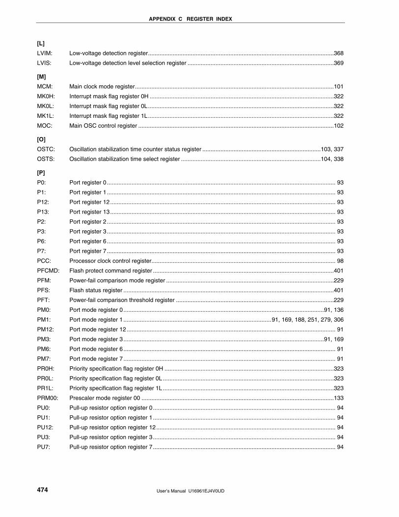
APPENDIX C REGISTER INDEX
User’s Manual U16961EJ4V0UD 474
[L]
LVIM: Low-voltage detection register.................................................................................................................368
LVIS: Low-voltage detection level selection register .........................................................................................369
[M]
MCM: Main clock mode register.........................................................................................................................101
MK0H: Interrupt mask flag register 0H ................................................................................................................322
MK0L: Interrupt mask flag register 0L.................................................................................................................322
MK1L: Interrupt mask flag register 1L.................................................................................................................322
MOC: Main OSC control register .......................................................................................................................102
[O]
OSTC: Oscillation stabilization time counter status register ........................................................................103, 337
OSTS: Oscillation stabilization time select register .....................................................................................104, 338
[P]
P0: Port register 0........................................................................................................................................... 93
P1: Port register 1........................................................................................................................................... 93
P12: Port register 12......................................................................................................................................... 93
P13: Port register 13......................................................................................................................................... 93
P2: Port register 2........................................................................................................................................... 93
P3: Port register 3........................................................................................................................................... 93
P6: Port register 6........................................................................................................................................... 93
P7: Port register 7........................................................................................................................................... 93
PCC: Processor clock control register................................................................................................................ 98
PFCMD: Flash protect command register ..............................................................................................................401
PFM: Power-fail comparison mode register ......................................................................................................229
PFS: Flash status register ................................................................................................................................401
PFT: Power-fail comparison threshold register ................................................................................................229
PM0: Port mode register 0 ..........................................................................................................................91, 136
PM1: Port mode register 1 ..........................................................................................91, 169, 188, 251, 279, 306
PM12: Port mode register 12 ............................................................................................................................... 91
PM3: Port mode register 3 ..........................................................................................................................91, 169
PM6: Port mode register 6 ................................................................................................................................. 91
PM7: Port mode register 7 ................................................................................................................................. 91
PR0H: Priority specification flag register 0H .......................................................................................................323
PR0L: Priority specification flag register 0L ........................................................................................................323
PR1L: Priority specification flag register 1L ........................................................................................................323
PRM00: Prescaler mode register 00 .....................................................................................................................133
PU0: Pull-up resistor option register 0............................................................................................................... 94
PU1: Pull-up resistor option register 1............................................................................................................... 94
PU12: Pull-up resistor option register 12............................................................................................................. 94
PU3: Pull-up resistor option register 3............................................................................................................... 94
PU7: Pull-up resistor option register 7............................................................................................................... 94
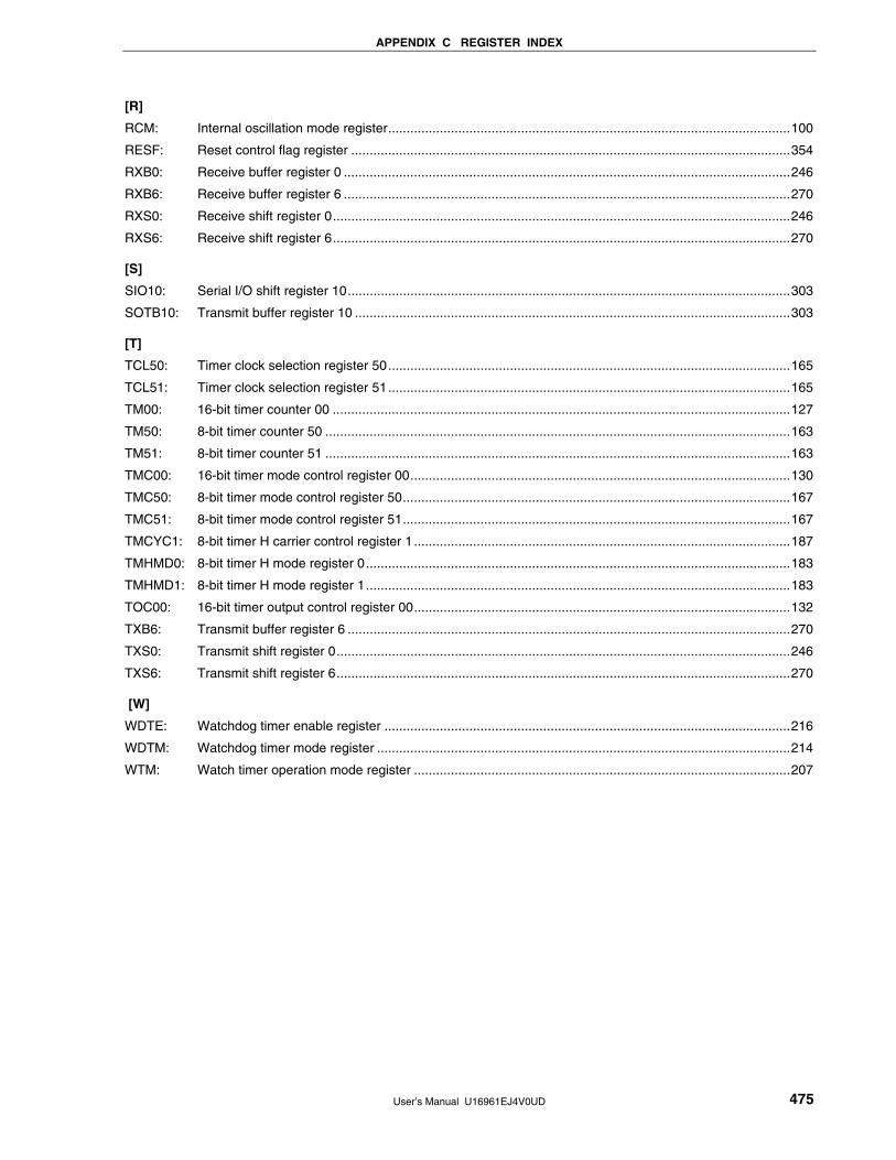
APPENDIX C REGISTER INDEX
User’s Manual U16961EJ4V0UD 475
[R]
RCM: Internal oscillation mode register.............................................................................................................100
RESF: Reset control flag register .......................................................................................................................354
RXB0: Receive buffer register 0 .........................................................................................................................246
RXB6: Receive buffer register 6 .........................................................................................................................270
RXS0: Receive shift register 0............................................................................................................................246
RXS6: Receive shift register 6............................................................................................................................270
[S]
SIO10: Serial I/O shift register 10........................................................................................................................303
SOTB10: Transmit buffer register 10 ......................................................................................................................303
[T]
TCL50: Timer clock selection register 50.............................................................................................................165
TCL51: Timer clock selection register 51.............................................................................................................165
TM00: 16-bit timer counter 00 ............................................................................................................................127
TM50: 8-bit timer counter 50 ..............................................................................................................................163
TM51: 8-bit timer counter 51 ..............................................................................................................................163
TMC00: 16-bit timer mode control register 00.......................................................................................................130
TMC50: 8-bit timer mode control register 50.........................................................................................................167
TMC51: 8-bit timer mode control register 51.........................................................................................................167
TMCYC1: 8-bit timer H carrier control register 1 ......................................................................................................187
TMHMD0: 8-bit timer H mode register 0...................................................................................................................183
TMHMD1: 8-bit timer H mode register 1...................................................................................................................183
TOC00: 16-bit timer output control register 00......................................................................................................132
TXB6: Transmit buffer register 6 ........................................................................................................................270
TXS0: Transmit shift register 0...........................................................................................................................246
TXS6: Transmit shift register 6...........................................................................................................................270
[W]
WDTE: Watchdog timer enable register ..............................................................................................................216
WDTM: Watchdog timer mode register ................................................................................................................214
WTM: Watch timer operation mode register ......................................................................................................207
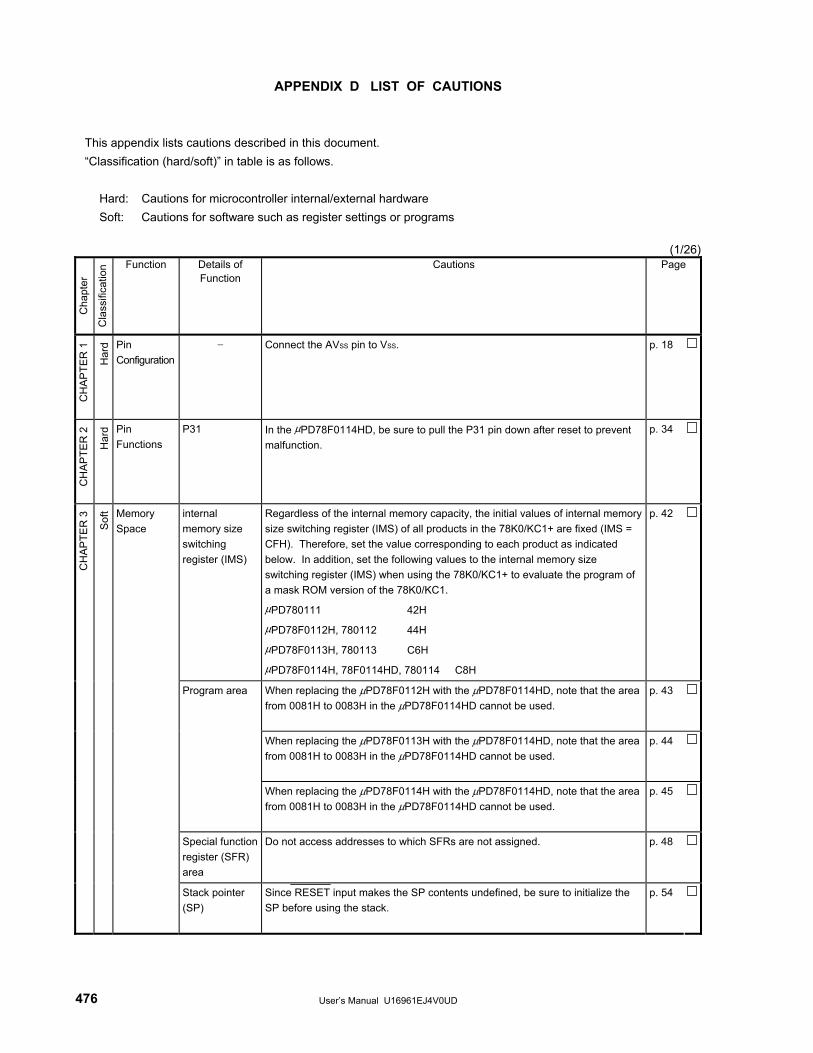
User’s Manual U16961EJ4V0UD 476
APPENDIX D LIST OF CAUTIONS
This appendix lists cautions described in this document. “Classification (hard/soft)” in table is as follows.
Hard: Cautions for microcontroller internal/external hardware Soft: Cautions for software such as register settings or programs
(1/26)
Cha
pter
Cla
ssifi
catio
n Function Details of Function
Cautions Page
CH
AP
TER
1
Har
d Pin Configuration
− Connect the AVSS pin to VSS. p. 18
CH
AP
TER
2
Har
d Pin Functions
P31 In the μPD78F0114HD, be sure to pull the P31 pin down after reset to prevent malfunction.
p. 34
internal memory size switching register (IMS)
Regardless of the internal memory capacity, the initial values of internal memory size switching register (IMS) of all products in the 78K0/KC1+ are fixed (IMS = CFH). Therefore, set the value corresponding to each product as indicated below. In addition, set the following values to the internal memory size switching register (IMS) when using the 78K0/KC1+ to evaluate the program of a mask ROM version of the 78K0/KC1.
μPD780111 42H
μPD78F0112H, 780112 44H
μPD78F0113H, 780113 C6H
μPD78F0114H, 78F0114HD, 780114 C8H
p. 42
When replacing the μPD78F0112H with the μPD78F0114HD, note that the area from 0081H to 0083H in the μPD78F0114HD cannot be used.
p. 43
When replacing the μPD78F0113H with the μPD78F0114HD, note that the area from 0081H to 0083H in the μPD78F0114HD cannot be used.
p. 44
Program area
When replacing the μPD78F0114H with the μPD78F0114HD, note that the area from 0081H to 0083H in the μPD78F0114HD cannot be used.
p. 45
Special function register (SFR) area
Do not access addresses to which SFRs are not assigned. p. 48
CH
AP
TER
3
Sof
t Memory Space
Stack pointer (SP)
Since RESET input makes the SP contents undefined, be sure to initialize the SP before using the stack.
p. 54
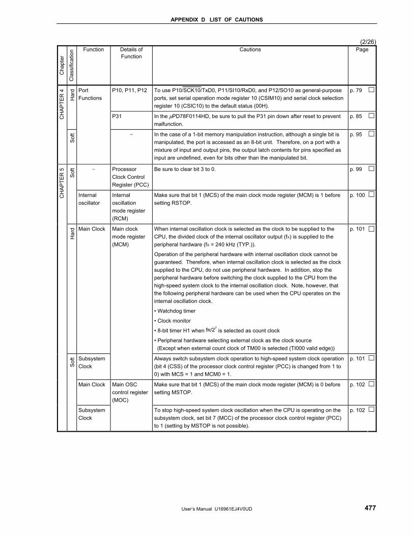
APPENDIX D LIST OF CAUTIONS
User’s Manual U16961EJ4V0UD 477
(2/26)
Cha
pter
Cla
ssifi
catio
n Function Details of Function
Cautions Page
P10, P11, P12 To use P10/SCK10/TxD0, P11/SI10/RxD0, and P12/SO10 as general-purpose ports, set serial operation mode register 10 (CSIM10) and serial clock selection register 10 (CSIC10) to the default status (00H).
p. 79
Har
d
P31 In the μPD78F0114HD, be sure to pull the P31 pin down after reset to prevent malfunction.
p. 85 CH
AP
TER
4
Sof
t
Port Functions
− In the case of a 1-bit memory manipulation instruction, although a single bit is manipulated, the port is accessed as an 8-bit unit. Therefore, on a port with a mixture of input and output pins, the output latch contents for pins specified as input are undefined, even for bits other than the manipulated bit.
p. 95
− Processor Clock Control Register (PCC)
Be sure to clear bit 3 to 0. p. 99
Sof
t
Internal oscillator
Internal oscillation mode register (RCM)
Make sure that bit 1 (MCS) of the main clock mode register (MCM) is 1 before setting RSTOP.
p. 100
Har
d Main Clock When internal oscillation clock is selected as the clock to be supplied to the CPU, the divided clock of the internal oscillator output (fX) is supplied to the peripheral hardware (fX = 240 kHz (TYP.)).
Operation of the peripheral hardware with internal oscillation clock cannot be guaranteed. Therefore, when internal oscillation clock is selected as the clock supplied to the CPU, do not use peripheral hardware. In addition, stop the peripheral hardware before switching the clock supplied to the CPU from the high-speed system clock to the internal oscillation clock. Note, however, that the following peripheral hardware can be used when the CPU operates on the internal oscillation clock.
• Watchdog timer
• Clock monitor
• 8-bit timer H1 when fR/27 is selected as count clock
• Peripheral hardware selecting external clock as the clock source (Except when external count clock of TM00 is selected (TI000 valid edge))
p. 101
Subsystem Clock
Main clock mode register (MCM)
Always switch subsystem clock operation to high-speed system clock operation (bit 4 (CSS) of the processor clock control register (PCC) is changed from 1 to 0) with MCS = 1 and MCM0 = 1.
p. 101
Main Clock Make sure that bit 1 (MCS) of the main clock mode register (MCM) is 0 before setting MSTOP.
p. 102
CH
AP
TER
5
Sof
t
Subsystem Clock
Main OSC control register (MOC)
To stop high-speed system clock oscillation when the CPU is operating on the subsystem clock, set bit 7 (MCC) of the processor clock control register (PCC) to 1 (setting by MSTOP is not possible).
p. 102
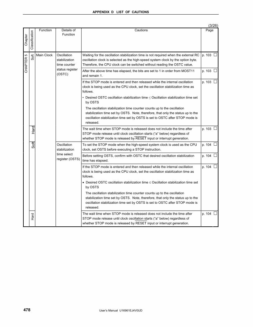
APPENDIX D LIST OF CAUTIONS
User’s Manual U16961EJ4V0UD 478
(3/26) C
hapt
er
Cla
ssifi
catio
n Function Details of Function
Cautions Page
Waiting for the oscillation stabilization time is not required when the external RC oscillation clock is selected as the high-speed system clock by the option byte. Therefore, the CPU clock can be switched without reading the OSTC value.
p. 103
After the above time has elapsed, the bits are set to 1 in order from MOST11 and remain 1.
p. 103
Sof
t
If the STOP mode is entered and then released while the internal oscillation clock is being used as the CPU clock, set the oscillation stabilization time as follows.
• Desired OSTC oscillation stabilization time ≤ Oscillation stabilization time set by OSTS
The oscillation stabilization time counter counts up to the oscillation stabilization time set by OSTS. Note, therefore, that only the status up to the oscillation stabilization time set by OSTS is set to OSTC after STOP mode is released.
p. 103
Har
d
Oscillation stabilization time counter status register (OSTC)
The wait time when STOP mode is released does not include the time after STOP mode release until clock oscillation starts (“a” below) regardless of whether STOP mode is released by RESET input or interrupt generation.
p. 103
To set the STOP mode when the high-speed system clock is used as the CPU clock, set OSTS before executing a STOP instruction.
p. 104
Before setting OSTS, confirm with OSTC that desired oscillation stabilization time has elapsed.
p. 104
Sof
t
If the STOP mode is entered and then released while the internal oscillation clock is being used as the CPU clock, set the oscillation stabilization time as follows.
• Desired OSTC oscillation stabilization time ≤ Oscillation stabilization time set by OSTS
The oscillation stabilization time counter counts up to the oscillation stabilization time set by OSTS. Note, therefore, that only the status up to the oscillation stabilization time set by OSTS is set to OSTC after STOP mode is released.
p. 104
CH
AP
TER
5
Har
d
Main Clock
Oscillation stabilization time select register (OSTS)
The wait time when STOP mode is released does not include the time after STOP mode release until clock oscillation starts (“a” below) regardless of whether STOP mode is released by RESET input or interrupt generation.
p. 104
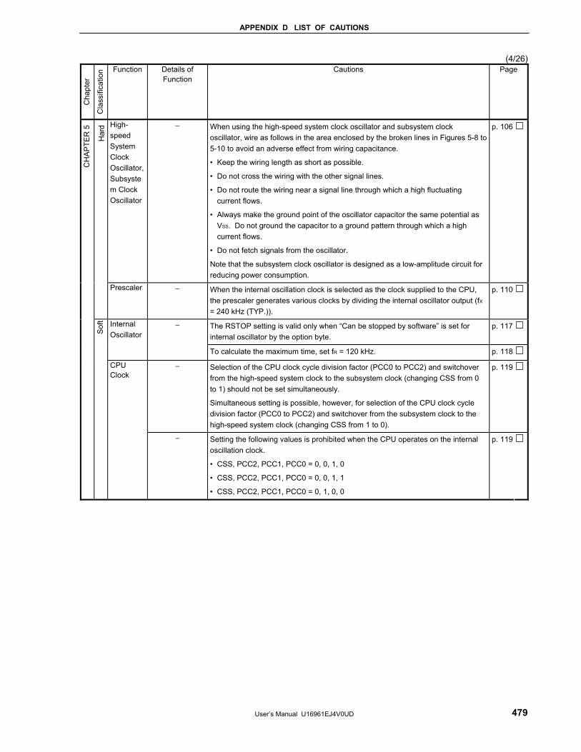
APPENDIX D LIST OF CAUTIONS
User’s Manual U16961EJ4V0UD 479
(4/26)
Cha
pter
Cla
ssifi
catio
n Function Details of Function
Cautions Page
High-speed System Clock Oscillator, Subsystem Clock Oscillator
− When using the high-speed system clock oscillator and subsystem clock oscillator, wire as follows in the area enclosed by the broken lines in Figures 5-8 to 5-10 to avoid an adverse effect from wiring capacitance.
• Keep the wiring length as short as possible.
• Do not cross the wiring with the other signal lines.
• Do not route the wiring near a signal line through which a high fluctuating current flows.
• Always make the ground point of the oscillator capacitor the same potential as VSS. Do not ground the capacitor to a ground pattern through which a high current flows.
• Do not fetch signals from the oscillator.
Note that the subsystem clock oscillator is designed as a low-amplitude circuit for reducing power consumption.
p. 106
Har
d
Prescaler − When the internal oscillation clock is selected as the clock supplied to the CPU, the prescaler generates various clocks by dividing the internal oscillator output (fX = 240 kHz (TYP.)).
p. 110
The RSTOP setting is valid only when “Can be stopped by software” is set for internal oscillator by the option byte.
p. 117Internal Oscillator
−
To calculate the maximum time, set fR = 120 kHz. p. 118
− Selection of the CPU clock cycle division factor (PCC0 to PCC2) and switchover from the high-speed system clock to the subsystem clock (changing CSS from 0 to 1) should not be set simultaneously.
Simultaneous setting is possible, however, for selection of the CPU clock cycle division factor (PCC0 to PCC2) and switchover from the subsystem clock to the high-speed system clock (changing CSS from 1 to 0).
p. 119
CH
AP
TER
5
Sof
t
CPU Clock
− Setting the following values is prohibited when the CPU operates on the internal oscillation clock.
• CSS, PCC2, PCC1, PCC0 = 0, 0, 1, 0
• CSS, PCC2, PCC1, PCC0 = 0, 0, 1, 1
• CSS, PCC2, PCC1, PCC0 = 0, 1, 0, 0
p. 119
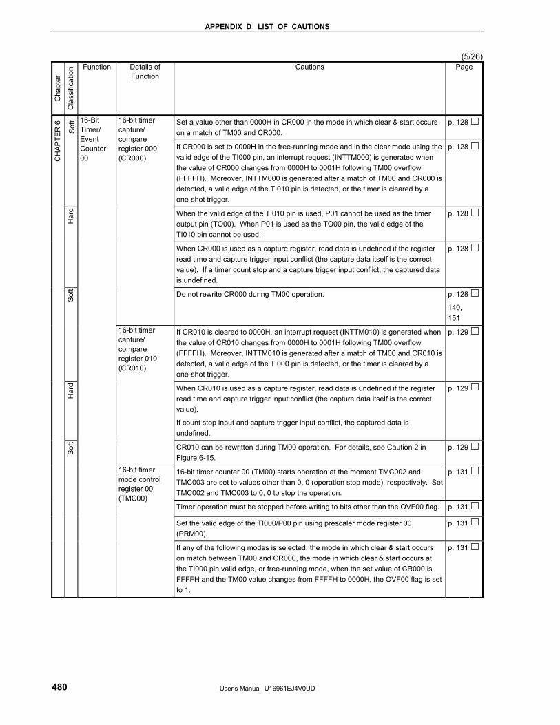
APPENDIX D LIST OF CAUTIONS
User’s Manual U16961EJ4V0UD 480
(5/26) C
hapt
er
Cla
ssifi
catio
n Function Details of Function
Cautions Page
Set a value other than 0000H in CR000 in the mode in which clear & start occurs on a match of TM00 and CR000.
p. 128
Sof
t
If CR000 is set to 0000H in the free-running mode and in the clear mode using the valid edge of the TI000 pin, an interrupt request (INTTM000) is generated when the value of CR000 changes from 0000H to 0001H following TM00 overflow (FFFFH). Moreover, INTTM000 is generated after a match of TM00 and CR000 is detected, a valid edge of the TI010 pin is detected, or the timer is cleared by a one-shot trigger.
p. 128
When the valid edge of the TI010 pin is used, P01 cannot be used as the timer output pin (TO00). When P01 is used as the TO00 pin, the valid edge of the TI010 pin cannot be used.
p. 128
Har
d
When CR000 is used as a capture register, read data is undefined if the register read time and capture trigger input conflict (the capture data itself is the correct value). If a timer count stop and a capture trigger input conflict, the captured data is undefined.
p. 128
16-bit timer capture/ compare register 000 (CR000)
Do not rewrite CR000 during TM00 operation. p. 128
140, 151
Sof
t
If CR010 is cleared to 0000H, an interrupt request (INTTM010) is generated when the value of CR010 changes from 0000H to 0001H following TM00 overflow (FFFFH). Moreover, INTTM010 is generated after a match of TM00 and CR010 is detected, a valid edge of the TI000 pin is detected, or the timer is cleared by a one-shot trigger.
p. 129
Har
d When CR010 is used as a capture register, read data is undefined if the register read time and capture trigger input conflict (the capture data itself is the correct value).
If count stop input and capture trigger input conflict, the captured data is undefined.
p. 129
16-bit timer capture/ compare register 010 (CR010)
CR010 can be rewritten during TM00 operation. For details, see Caution 2 in Figure 6-15.
p. 129
16-bit timer counter 00 (TM00) starts operation at the moment TMC002 and TMC003 are set to values other than 0, 0 (operation stop mode), respectively. Set TMC002 and TMC003 to 0, 0 to stop the operation.
p. 131
Timer operation must be stopped before writing to bits other than the OVF00 flag. p. 131
Set the valid edge of the TI000/P00 pin using prescaler mode register 00 (PRM00).
p. 131
CH
AP
TER
6
Sof
t
16-Bit Timer/ Event Counter 00
16-bit timer mode control register 00 (TMC00)
If any of the following modes is selected: the mode in which clear & start occurs on match between TM00 and CR000, the mode in which clear & start occurs at the TI000 pin valid edge, or free-running mode, when the set value of CR000 is FFFFH and the TM00 value changes from FFFFH to 0000H, the OVF00 flag is set to 1.
p. 131
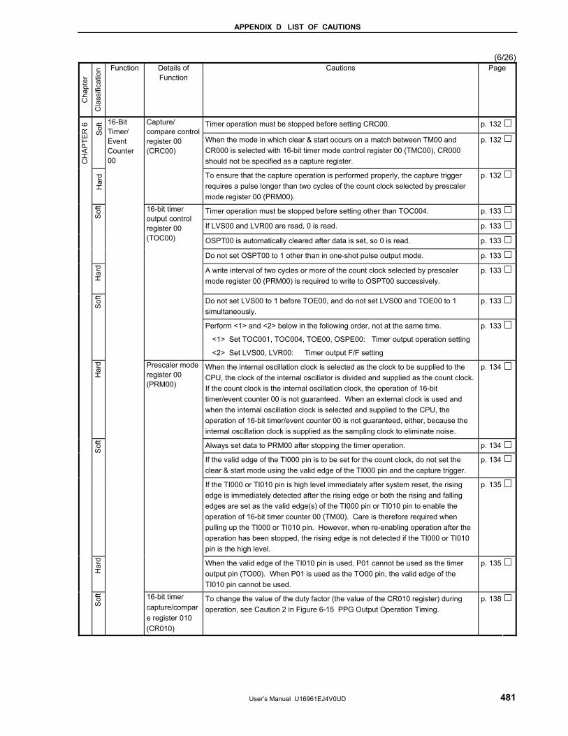
APPENDIX D LIST OF CAUTIONS
User’s Manual U16961EJ4V0UD 481
(6/26)
Cha
pter
Cla
ssifi
catio
n Function Details of Function
Cautions Page
Timer operation must be stopped before setting CRC00. p. 132
Sof
t
When the mode in which clear & start occurs on a match between TM00 and CR000 is selected with 16-bit timer mode control register 00 (TMC00), CR000 should not be specified as a capture register.
p. 132
Har
d
Capture/ compare control register 00 (CRC00)
To ensure that the capture operation is performed properly, the capture trigger requires a pulse longer than two cycles of the count clock selected by prescaler mode register 00 (PRM00).
p. 132
Timer operation must be stopped before setting other than TOC004. p. 133
If LVS00 and LVR00 are read, 0 is read. p. 133
OSPT00 is automatically cleared after data is set, so 0 is read. p. 133
Sof
t
Do not set OSPT00 to 1 other than in one-shot pulse output mode. p. 133
Har
d A write interval of two cycles or more of the count clock selected by prescaler mode register 00 (PRM00) is required to write to OSPT00 successively.
p. 133
Do not set LVS00 to 1 before TOE00, and do not set LVS00 and TOE00 to 1 simultaneously.
p. 133
Sof
t
16-bit timer output control register 00 (TOC00)
Perform <1> and <2> below in the following order, not at the same time.
<1> Set TOC001, TOC004, TOE00, OSPE00: Timer output operation setting
<2> Set LVS00, LVR00: Timer output F/F setting
p. 133
Har
d When the internal oscillation clock is selected as the clock to be supplied to the CPU, the clock of the internal oscillator is divided and supplied as the count clock. If the count clock is the internal oscillation clock, the operation of 16-bit timer/event counter 00 is not guaranteed. When an external clock is used and when the internal oscillation clock is selected and supplied to the CPU, the operation of 16-bit timer/event counter 00 is not guaranteed, either, because the internal oscillation clock is supplied as the sampling clock to eliminate noise.
p. 134
Always set data to PRM00 after stopping the timer operation. p. 134
If the valid edge of the TI000 pin is to be set for the count clock, do not set the clear & start mode using the valid edge of the TI000 pin and the capture trigger.
p. 134
Sof
t
If the TI000 or TI010 pin is high level immediately after system reset, the rising edge is immediately detected after the rising edge or both the rising and falling edges are set as the valid edge(s) of the TI000 pin or TI010 pin to enable the operation of 16-bit timer counter 00 (TM00). Care is therefore required when pulling up the TI000 or TI010 pin. However, when re-enabling operation after the operation has been stopped, the rising edge is not detected if the TI000 or TI010 pin is the high level.
p. 135
Har
d
Prescaler mode register 00 (PRM00)
When the valid edge of the TI010 pin is used, P01 cannot be used as the timer output pin (TO00). When P01 is used as the TO00 pin, the valid edge of the TI010 pin cannot be used.
p. 135
CH
AP
TER
6
Sof
t
16-Bit Timer/ Event Counter 00
16-bit timer capture/compare register 010 (CR010)
To change the value of the duty factor (the value of the CR010 register) during operation, see Caution 2 in Figure 6-15 PPG Output Operation Timing.
p. 138
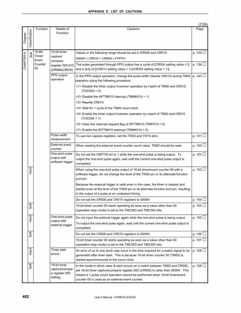
APPENDIX D LIST OF CAUTIONS
User’s Manual U16961EJ4V0UD 482
(7/26) C
hapt
er
Cla
ssifi
catio
n Function Details of Function
Cautions Page
Values in the following range should be set in CR000 and CR010:
0000H ≤ CR010 < CR000 ≤ FFFFH
p. 13916-bit timer capture/ compare register 000,010 (CR0000,CR010)
The pulse generated through PPG output has a cycle of [CR00n setting value +1], and a duty of [(CR01n setting value + 1)/(CR00n setting value + 1)].
p. 139
PPG output operation
In the PPG output operation, change the pulse width (rewrite CR010) during TM00 operation using the following procedure.
<1> Disable the timer output inversion operation by match of TM00 and CR010 (TOC004 = 0)
<2> Disable the INTTM010 interrupt (TMMK010 = 1)
<3> Rewrite CR010
<4> Wait for 1 cycle of the TM00 count clock
<5> Enable the timer output inversion operation by match of TM00 and CR010 (TOC004 = 1)
<6> Clear the interrupt request flag of INTTM010 (TMIF010 = 0)
<7> Enable the INTTM010 interrupt (TMMK010 = 0)
p. 140
Pulse width measurement
To use two capture registers, set the TI000 and TI010 pins. p. 141
External event counter
When reading the external event counter count value, TM00 should be read. p. 150
Sof
t
Do not set the OSPT00 bit to 1 while the one-shot pulse is being output. To output the one-shot pulse again, wait until the current one-shot pulse output is completed.
p. 153
When using the one-shot pulse output of 16-bit timer/event counter 00 with a software trigger, do not change the level of the TI000 pin or its alternate-function port pin.
Because the external trigger is valid even in this case, the timer is cleared and started even at the level of the TI000 pin or its alternate-function port pin, resulting in the output of a pulse at an undesired timing.
p. 153
Har
d
Do not set the CR000 and CR010 registers to 0000H. p. 154
Sof
t
One-shot pulse output with software trigger
16-bit timer counter 00 starts operating as soon as a value other than 00 (operation stop mode) is set to the TMC003 and TMC002 bits.
p. 155
Har
d Do not input the external trigger again while the one-shot pulse is being output.
To output the one-shot pulse again, wait until the current one-shot pulse output is completed.
p. 155
Do not set the CR000 and CR010 registers to 0000H. p. 156
Sof
t
One-shot pulse output with external trigger
16-bit timer counter 00 starts operating as soon as a value other than 00 (operation stop mode) is set to the TMC003 and TMC002 bits.
p. 157
Har
d Timer start errors
An error of up to one clock may occur in the time required for a match signal to be generated after timer start. This is because 16-bit timer counter 00 (TM00) is started asynchronously to the count clock.
p. 158
CH
AP
TER
6
Sof
t
16-Bit Timer/ Event Counter 00
16-bit timer capture/compare register 000 setting
In the mode in which clear & start occurs on a match between TM00 and CR000, set 16-bit timer capture/compare register 000 (CR000) to other than 0000H. This means a 1-pulse count operation cannot be performed when 16-bit timer/event counter 00 is used as an external event counter.
p. 158
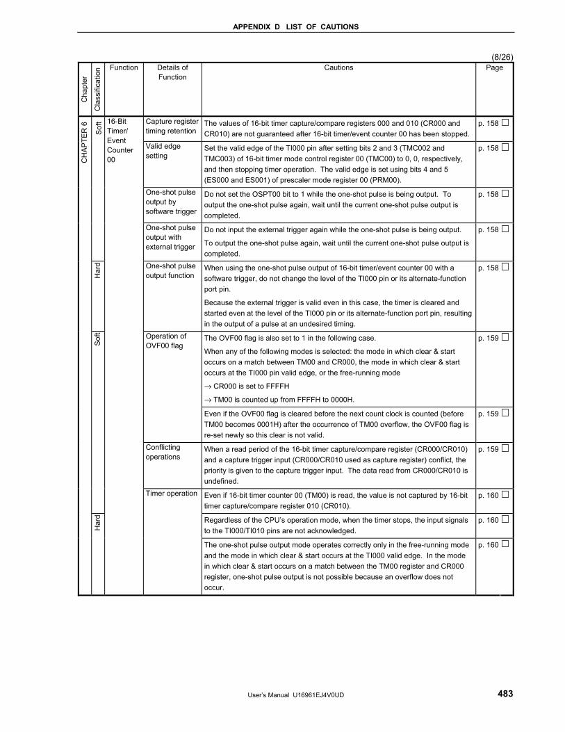
APPENDIX D LIST OF CAUTIONS
User’s Manual U16961EJ4V0UD 483
(8/26)
Cha
pter
Cla
ssifi
catio
n Function Details of Function
Cautions Page
Capture register timing retention
The values of 16-bit timer capture/compare registers 000 and 010 (CR000 and CR010) are not guaranteed after 16-bit timer/event counter 00 has been stopped.
p. 158
Valid edge setting
Set the valid edge of the TI000 pin after setting bits 2 and 3 (TMC002 and TMC003) of 16-bit timer mode control register 00 (TMC00) to 0, 0, respectively, and then stopping timer operation. The valid edge is set using bits 4 and 5 (ES000 and ES001) of prescaler mode register 00 (PRM00).
p. 158
One-shot pulse output by software trigger
Do not set the OSPT00 bit to 1 while the one-shot pulse is being output. To output the one-shot pulse again, wait until the current one-shot pulse output is completed.
p. 158
Sof
t
One-shot pulse output with external trigger
Do not input the external trigger again while the one-shot pulse is being output.
To output the one-shot pulse again, wait until the current one-shot pulse output is completed.
p. 158
Har
d One-shot pulse output function
When using the one-shot pulse output of 16-bit timer/event counter 00 with a software trigger, do not change the level of the TI000 pin or its alternate-function port pin.
Because the external trigger is valid even in this case, the timer is cleared and started even at the level of the TI000 pin or its alternate-function port pin, resulting in the output of a pulse at an undesired timing.
p. 158
The OVF00 flag is also set to 1 in the following case.
When any of the following modes is selected: the mode in which clear & start occurs on a match between TM00 and CR000, the mode in which clear & start occurs at the TI000 pin valid edge, or the free-running mode
→ CR000 is set to FFFFH
→ TM00 is counted up from FFFFH to 0000H.
p. 159Operation of OVF00 flag
Even if the OVF00 flag is cleared before the next count clock is counted (before TM00 becomes 0001H) after the occurrence of TM00 overflow, the OVF00 flag is re-set newly so this clear is not valid.
p. 159
Conflicting operations
When a read period of the 16-bit timer capture/compare register (CR000/CR010) and a capture trigger input (CR000/CR010 used as capture register) conflict, the priority is given to the capture trigger input. The data read from CR000/CR010 is undefined.
p. 159
Sof
t
Even if 16-bit timer counter 00 (TM00) is read, the value is not captured by 16-bit timer capture/compare register 010 (CR010).
p. 160
Regardless of the CPU’s operation mode, when the timer stops, the input signals to the TI000/TI010 pins are not acknowledged.
p. 160
CH
AP
TER
6
Har
d
16-Bit Timer/ Event Counter 00
Timer operation
The one-shot pulse output mode operates correctly only in the free-running mode and the mode in which clear & start occurs at the TI000 valid edge. In the mode in which clear & start occurs on a match between the TM00 register and CR000 register, one-shot pulse output is not possible because an overflow does not occur.
p. 160
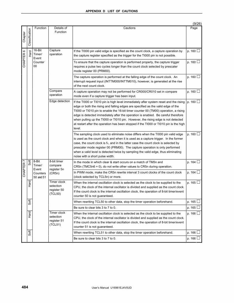
APPENDIX D LIST OF CAUTIONS
User’s Manual U16961EJ4V0UD 484
(9/26) C
hapt
er
Cla
ssifi
catio
n Function Details of Function
Cautions Page
If the TI000 pin valid edge is specified as the count clock, a capture operation by the capture register specified as the trigger for the TI000 pin is not possible.
p. 160
To ensure that the capture operation is performed properly, the capture trigger requires a pulse two cycles longer than the count clock selected by prescaler mode register 00 (PRM00).
p. 160
Capture operation
The capture operation is performed at the falling edge of the count clock. An interrupt request input (INTTM000/INTTM010), however, is generated at the rise of the next count clock.
p. 160
Compare operation
A capture operation may not be performed for CR000/CR010 set in compare mode even if a capture trigger has been input.
p. 160
If the TI000 or TI010 pin is high level immediately after system reset and the rising edge or both the rising and falling edges are specified as the valid edge of the TI000 or TI010 pin to enable the 16-bit timer counter 00 (TM00) operation, a rising edge is detected immediately after the operation is enabled. Be careful therefore when pulling up the TI000 or TI010 pin. However, the rising edge is not detected at restart after the operation has been stopped if the TI000 or TI010 pin is the high level.
p. 160
CH
AP
TER
6
Har
d 16-Bit Timer/ Event Counter 00
Edge detection
The sampling clock used to eliminate noise differs when the TI000 pin valid edge is used as the count clock and when it is used as a capture trigger. In the former case, the count clock is fX, and in the latter case the count clock is selected by prescaler mode register 00 (PRM00). The capture operation is only performed when a valid level is detected twice by sampling the valid edge, thus eliminating noise with a short pulse width.
p. 160
In the mode in which clear & start occurs on a match of TM5n and CR5n (TMC5n6 = 0), do not write other values to CR5n during operation.
p. 164
Sof
t 8-bit timer compare register 5n (CR5n) In PWM mode, make the CR5n rewrite interval 3 count clocks of the count clock
(clock selected by TCL5n) or more. p. 164
Har
d When the internal oscillation clock is selected as the clock to be supplied to the CPU, the clock of the internal oscillator is divided and supplied as the count clock. If the count clock is the internal oscillation clock, the operation of 8-bit timer/event counter 50 is not guaranteed.
p. 165
When rewriting TCL50 to other data, stop the timer operation beforehand. p. 165
Sof
t
Timer clock selection register 50 (TCL50)
Be sure to clear bits 3 to 7 to 0. p. 165
Har
d When the internal oscillation clock is selected as the clock to be supplied to the CPU, the clock of the internal oscillator is divided and supplied as the count clock. If the count clock is the internal oscillation clock, the operation of 8-bit timer/event counter 51 is not guaranteed.
p. 166
When rewriting TCL51 to other data, stop the timer operation beforehand. p. 166
CH
AP
TER
7
Sof
t
8-Bit Timer/ Event Counters 50 and 51
Timer clock selection register 51 (TCL51)
Be sure to clear bits 3 to 7 to 0. p. 166
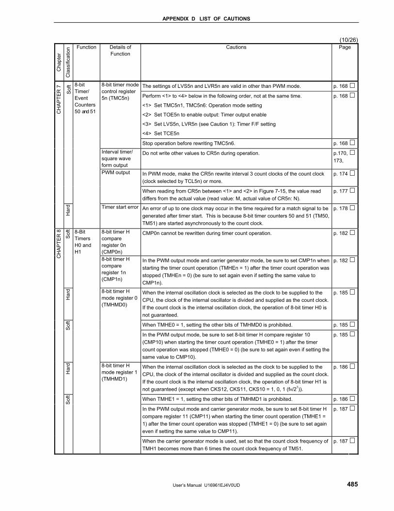
APPENDIX D LIST OF CAUTIONS
User’s Manual U16961EJ4V0UD 485
(10/26)
Cha
pter
Cla
ssifi
catio
n Function Details of Function
Cautions Page
The settings of LVS5n and LVR5n are valid in other than PWM mode. p. 168
Perform <1> to <4> below in the following order, not at the same time.
<1> Set TMC5n1, TMC5n6: Operation mode setting
<2> Set TOE5n to enable output: Timer output enable
<3> Set LVS5n, LVR5n (see Caution 1): Timer F/F setting
<4> Set TCE5n
p. 168
8-bit timer mode control register 5n (TMC5n)
Stop operation before rewriting TMC5n6. p. 168Interval timer/ square wave form output
Do not write other values to CR5n during operation. p.170,173,
In PWM mode, make the CR5n rewrite interval 3 count clocks of the count clock (clock selected by TCL5n) or more.
p. 174
Sof
t
PWM output
When reading from CR5n between <1> and <2> in Figure 7-15, the value read differs from the actual value (read value: M, actual value of CR5n: N).
p. 177
CH
AP
TER
7
Har
d
8-bit Timer/ Event Counters 50 and 51
Timer start error An error of up to one clock may occur in the time required for a match signal to be generated after timer start. This is because 8-bit timer counters 50 and 51 (TM50, TM51) are started asynchronously to the count clock.
p. 178
8-bit timer H compare register 0n (CMP0n)
CMP0n cannot be rewritten during timer count operation. p. 182
Sof
t
8-bit timer H compare register 1n (CMP1n)
In the PWM output mode and carrier generator mode, be sure to set CMP1n when starting the timer count operation (TMHEn = 1) after the timer count operation was stopped (TMHEn = 0) (be sure to set again even if setting the same value to CMP1n).
p. 182
Har
d When the internal oscillation clock is selected as the clock to be supplied to the CPU, the clock of the internal oscillator is divided and supplied as the count clock. If the count clock is the internal oscillation clock, the operation of 8-bit timer H0 is not guaranteed.
p. 185
When TMHE0 = 1, setting the other bits of TMHMD0 is prohibited. p. 185
Sof
t
8-bit timer H mode register 0 (TMHMD0)
In the PWM output mode, be sure to set 8-bit timer H compare register 10 (CMP10) when starting the timer count operation (TMHE0 = 1) after the timer count operation was stopped (TMHE0 = 0) (be sure to set again even if setting the same value to CMP10).
p. 185
Har
d When the internal oscillation clock is selected as the clock to be supplied to the CPU, the clock of the internal oscillator is divided and supplied as the count clock. If the count clock is the internal oscillation clock, the operation of 8-bit timer H1 is not guaranteed (except when CKS12, CKS11, CKS10 = 1, 0, 1 (fR/27)).
p. 186
When TMHE1 = 1, setting the other bits of TMHMD1 is prohibited. p. 186
In the PWM output mode and carrier generator mode, be sure to set 8-bit timer H compare register 11 (CMP11) when starting the timer count operation (TMHE1 = 1) after the timer count operation was stopped (TMHE1 = 0) (be sure to set again even if setting the same value to CMP11).
p. 187
CH
AP
TER
8
Sof
t
8-Bit Timers H0 and H1
8-bit timer H mode register 1 (TMHMD1)
When the carrier generator mode is used, set so that the count clock frequency of TMH1 becomes more than 6 times the count clock frequency of TM51.
p. 187
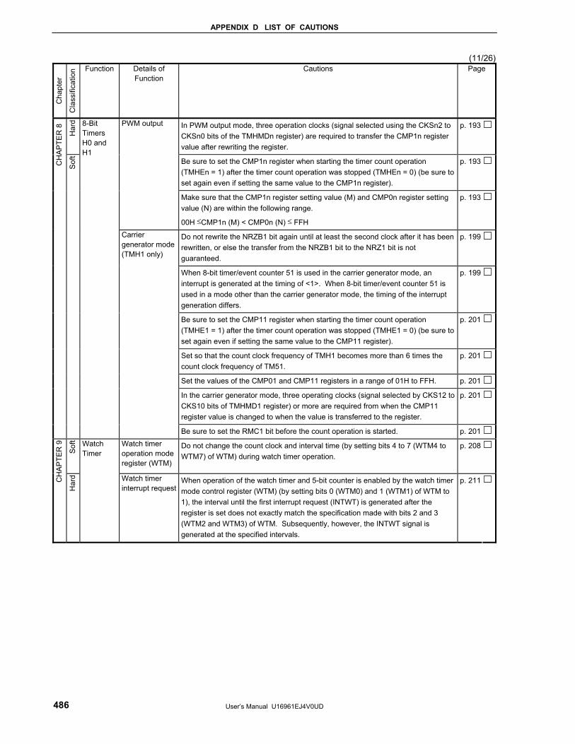
APPENDIX D LIST OF CAUTIONS
User’s Manual U16961EJ4V0UD 486
(11/26) C
hapt
er
Cla
ssifi
catio
n Function Details of Function
Cautions Page H
ard In PWM output mode, three operation clocks (signal selected using the CKSn2 to
CKSn0 bits of the TMHMDn register) are required to transfer the CMP1n register value after rewriting the register.
p. 193
Be sure to set the CMP1n register when starting the timer count operation (TMHEn = 1) after the timer count operation was stopped (TMHEn = 0) (be sure to set again even if setting the same value to the CMP1n register).
p. 193
PWM output
Make sure that the CMP1n register setting value (M) and CMP0n register setting value (N) are within the following range.
00H ≤CMP1n (M) < CMP0n (N) ≤ FFH
p. 193
Do not rewrite the NRZB1 bit again until at least the second clock after it has been rewritten, or else the transfer from the NRZB1 bit to the NRZ1 bit is not guaranteed.
p. 199
When 8-bit timer/event counter 51 is used in the carrier generator mode, an interrupt is generated at the timing of <1>. When 8-bit timer/event counter 51 is used in a mode other than the carrier generator mode, the timing of the interrupt generation differs.
p. 199
Be sure to set the CMP11 register when starting the timer count operation (TMHE1 = 1) after the timer count operation was stopped (TMHE1 = 0) (be sure to set again even if setting the same value to the CMP11 register).
p. 201
Set so that the count clock frequency of TMH1 becomes more than 6 times the count clock frequency of TM51.
p. 201
Set the values of the CMP01 and CMP11 registers in a range of 01H to FFH. p. 201
In the carrier generator mode, three operating clocks (signal selected by CKS12 to CKS10 bits of TMHMD1 register) or more are required from when the CMP11 register value is changed to when the value is transferred to the register.
p. 201
CH
AP
TER
8
Sof
t
8-Bit Timers H0 and H1
Carrier generator mode (TMH1 only)
Be sure to set the RMC1 bit before the count operation is started. p. 201
Sof
t Watch timer operation mode register (WTM)
Do not change the count clock and interval time (by setting bits 4 to 7 (WTM4 to WTM7) of WTM) during watch timer operation.
p. 208
CH
AP
TER
9
Har
d
Watch Timer
Watch timer interrupt request
When operation of the watch timer and 5-bit counter is enabled by the watch timer mode control register (WTM) (by setting bits 0 (WTM0) and 1 (WTM1) of WTM to 1), the interval until the first interrupt request (INTWT) is generated after the register is set does not exactly match the specification made with bits 2 and 3 (WTM2 and WTM3) of WTM. Subsequently, however, the INTWT signal is generated at the specified intervals.
p. 211
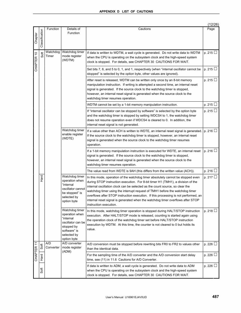
APPENDIX D LIST OF CAUTIONS
User’s Manual U16961EJ4V0UD 487
(12/26)
Cha
pter
Cla
ssifi
catio
n Function Details of Function
Cautions Page
If data is written to WDTM, a wait cycle is generated. Do not write data to WDTM when the CPU is operating on the subsystem clock and the high-speed system clock is stopped. For details, see CHAPTER 30 CAUTIONS FOR WAIT.
p. 215
Set bits 7, 6, and 5 to 0, 1, and 1, respectively (when “internal oscillator cannot be stopped” is selected by the option byte, other values are ignored).
p. 215
After reset is released, WDTM can be written only once by an 8-bit memory manipulation instruction. If writing is attempted a second time, an internal reset signal is generated. If the source clock to the watchdog timer is stopped, however, an internal reset signal is generated when the source clock to the watchdog timer resumes operation.
p. 215
WDTM cannot be set by a 1-bit memory manipulation instruction. p. 215
Watchdog timer mode register (WDTM)
If “internal oscillator can be stopped by software” is selected by the option byte and the watchdog timer is stopped by setting WDCS4 to 1, the watchdog timer does not resume operation even if WDCS4 is cleared to 0. In addition, the internal reset signal is not generated.
p. 215
If a value other than ACH is written to WDTE, an internal reset signal is generated. If the source clock to the watchdog timer is stopped, however, an internal reset signal is generated when the source clock to the watchdog timer resumes operation.
p. 216
If a 1-bit memory manipulation instruction is executed for WDTE, an internal reset signal is generated. If the source clock to the watchdog timer is stopped, however, an internal reset signal is generated when the source clock to the watchdog timer resumes operation.
p. 216
Sof
t
Watchdog timer enable register (WDTE)
The value read from WDTE is 9AH (this differs from the written value (ACH)). p. 216
Watchdog timer operation when “internal oscillator cannot be stopped” is selected by option byte
In this mode, operation of the watchdog timer absolutely cannot be stopped even during STOP instruction execution. For 8-bit timer H1 (TMH1), a division of the internal oscillation clock can be selected as the count source, so clear the watchdog timer using the interrupt request of TMH1 before the watchdog timer overflows after STOP instruction execution. If this processing is not performed, an internal reset signal is generated when the watchdog timer overflows after STOP instruction execution.
p. 217
CH
AP
TER
10
Har
d
Watchdog Timer
Watchdog timer operation when “internal oscillator can be stopped by software” is selected by option byte
In this mode, watchdog timer operation is stopped during HALT/STOP instruction execution. After HALT/STOP mode is released, counting is started again using the operation clock of the watchdog timer set before HALT/STOP instruction execution by WDTM. At this time, the counter is not cleared to 0 but holds its value.
p. 218
Sof
t A/D conversion must be stopped before rewriting bits FR0 to FR2 to values other than the identical data.
p. 226
Har
d For the sampling time of the A/D converter and the A/D conversion start delay time, see (11) in 11.6 Cautions for A/D Converter.
p. 226
CH
AP
TER
11
Sof
t
A/D Converter
A/D converter mode register (ADM)
If data is written to ADM, a wait cycle is generated. Do not write data to ADM when the CPU is operating on the subsystem clock and the high-speed system clock is stopped. For details, see CHAPTER 30 CAUTIONS FOR WAIT.
p. 226
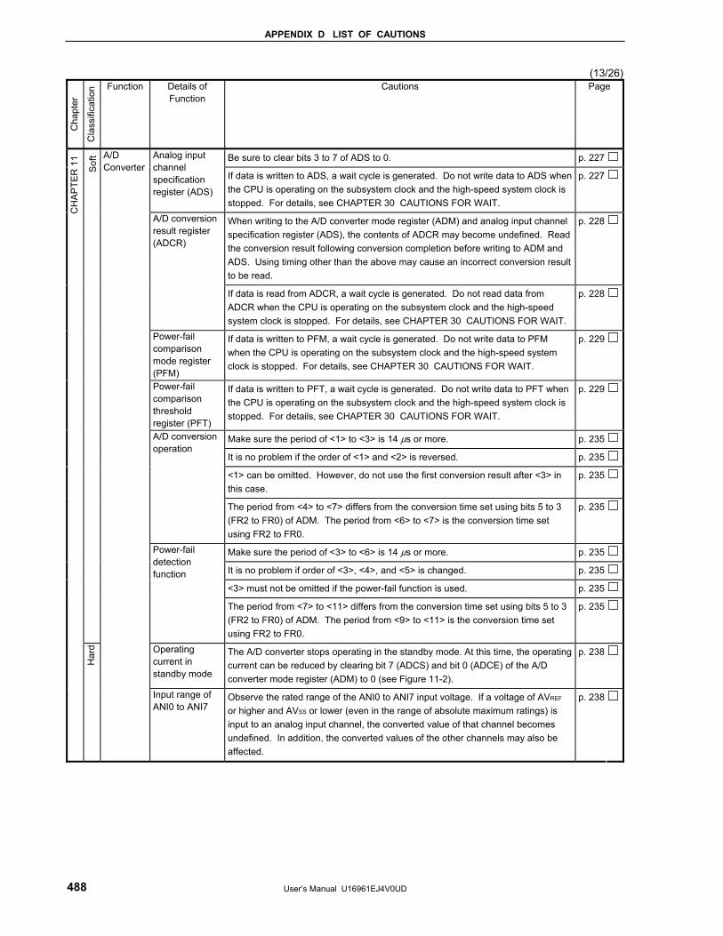
APPENDIX D LIST OF CAUTIONS
User’s Manual U16961EJ4V0UD 488
(13/26) C
hapt
er
Cla
ssifi
catio
n Function Details of Function
Cautions Page
Be sure to clear bits 3 to 7 of ADS to 0. p. 227Analog input channel specification register (ADS)
If data is written to ADS, a wait cycle is generated. Do not write data to ADS when the CPU is operating on the subsystem clock and the high-speed system clock is stopped. For details, see CHAPTER 30 CAUTIONS FOR WAIT.
p. 227
When writing to the A/D converter mode register (ADM) and analog input channel specification register (ADS), the contents of ADCR may become undefined. Read the conversion result following conversion completion before writing to ADM and ADS. Using timing other than the above may cause an incorrect conversion result to be read.
p. 228A/D conversion result register (ADCR)
If data is read from ADCR, a wait cycle is generated. Do not read data from ADCR when the CPU is operating on the subsystem clock and the high-speed system clock is stopped. For details, see CHAPTER 30 CAUTIONS FOR WAIT.
p. 228
Power-fail comparison mode register (PFM)
If data is written to PFM, a wait cycle is generated. Do not write data to PFM when the CPU is operating on the subsystem clock and the high-speed system clock is stopped. For details, see CHAPTER 30 CAUTIONS FOR WAIT.
p. 229
Power-fail comparison threshold register (PFT)
If data is written to PFT, a wait cycle is generated. Do not write data to PFT when the CPU is operating on the subsystem clock and the high-speed system clock is stopped. For details, see CHAPTER 30 CAUTIONS FOR WAIT.
p. 229
Make sure the period of <1> to <3> is 14 μs or more. p. 235
It is no problem if the order of <1> and <2> is reversed. p. 235
<1> can be omitted. However, do not use the first conversion result after <3> in this case.
p. 235
A/D conversion operation
The period from <4> to <7> differs from the conversion time set using bits 5 to 3 (FR2 to FR0) of ADM. The period from <6> to <7> is the conversion time set using FR2 to FR0.
p. 235
Make sure the period of <3> to <6> is 14 μs or more. p. 235
It is no problem if order of <3>, <4>, and <5> is changed. p. 235
<3> must not be omitted if the power-fail function is used. p. 235
Sof
t
Power-fail detection function
The period from <7> to <11> differs from the conversion time set using bits 5 to 3 (FR2 to FR0) of ADM. The period from <9> to <11> is the conversion time set using FR2 to FR0.
p. 235
Operating current in standby mode
The A/D converter stops operating in the standby mode. At this time, the operating current can be reduced by clearing bit 7 (ADCS) and bit 0 (ADCE) of the A/D converter mode register (ADM) to 0 (see Figure 11-2).
p. 238
CH
AP
TER
11
Har
d
A/D Converter
Input range of ANI0 to ANI7
Observe the rated range of the ANI0 to ANI7 input voltage. If a voltage of AVREF or higher and AVSS or lower (even in the range of absolute maximum ratings) is input to an analog input channel, the converted value of that channel becomes undefined. In addition, the converted values of the other channels may also be affected.
p. 238
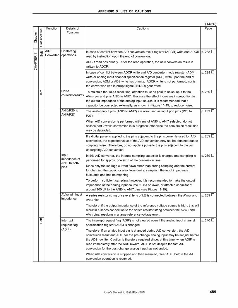
APPENDIX D LIST OF CAUTIONS
User’s Manual U16961EJ4V0UD 489
(14/26)
Cha
pter
Cla
ssifi
catio
n Function Details of Function
Cautions Page
In case of conflict between A/D conversion result register (ADCR) write and ADCR read by instruction upon the end of conversion,
ADCR read has priority. After the read operation, the new conversion result is written to ADCR.
p. 238
Sof
t Conflicting operations
In case of conflict between ADCR write and A/D converter mode register (ADM) write or analog input channel specification register (ADS) write upon the end of conversion, ADM or ADS write has priority. ADCR write is not performed, nor is the conversion end interrupt signal (INTAD) generated.
p. 238
Noise countermeasures
To maintain the 10-bit resolution, attention must be paid to noise input to the AVREF pin and pins ANI0 to ANI7. Because the effect increases in proportion to the output impedance of the analog input source, it is recommended that a capacitor be connected externally, as shown in Figure 11-19, to reduce noise.
p. 239
The analog input pins (ANI0 to ANI7) are also used as input port pins (P20 to P27).
When A/D conversion is performed with any of ANI0 to ANI7 selected, do not access port 2 while conversion is in progress; otherwise the conversion resolution may be degraded.
p. 239ANI0/P20 to ANI7/P27
If a digital pulse is applied to the pins adjacent to the pins currently used for A/D conversion, the expected value of the A/D conversion may not be obtained due to coupling noise. Therefore, do not apply a pulse to the pins adjacent to the pin undergoing A/D conversion.
p. 239
Input impedance of ANI0 to ANI7 pins
In this A/D converter, the internal sampling capacitor is charged and sampling is performed for approx. one sixth of the conversion time.
Since only the leakage current flows other than during sampling and the current for charging the capacitor also flows during sampling, the input impedance fluctuates and has no meaning.
To perform sufficient sampling, however, it is recommended to make the output impedance of the analog input source 10 kΩ or lower, or attach a capacitor of around 100 pF to the ANI0 to ANI7 pins (see Figure 11-19).
p. 239
Har
d
AVREF pin input impedance
A series resistor string of several tens of kΩ is connected between the AVREF and AVSS pins.
Therefore, if the output impedance of the reference voltage source is high, this will result in a series connection to the series resistor string between the AVREF and AVSS pins, resulting in a large reference voltage error.
p. 239
CH
AP
TER
11
Sof
t
A/D Converter
Interrupt request flag (ADIF)
The interrupt request flag (ADIF) is not cleared even if the analog input channel specification register (ADS) is changed.
Therefore, if an analog input pin is changed during A/D conversion, the A/D conversion result and ADIF for the pre-change analog input may be set just before the ADS rewrite. Caution is therefore required since, at this time, when ADIF is read immediately after the ADS rewrite, ADIF is set despite the fact A/D conversion for the post-change analog input has not ended.
When A/D conversion is stopped and then resumed, clear ADIF before the A/D conversion operation is resumed.
p. 240
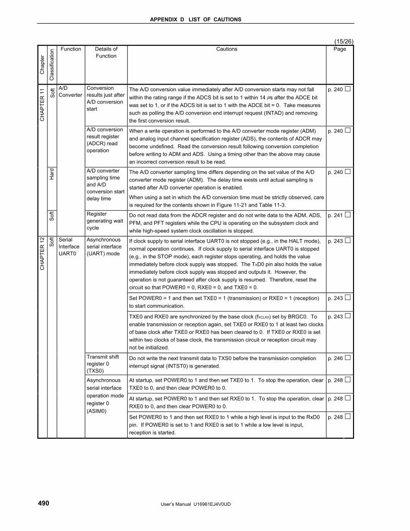
APPENDIX D LIST OF CAUTIONS
User’s Manual U16961EJ4V0UD 490
(15/26) C
hapt
er
Cla
ssifi
catio
n Function Details of Function
Cautions Page
Conversion results just after A/D conversion start
The A/D conversion value immediately after A/D conversion starts may not fall within the rating range if the ADCS bit is set to 1 within 14 μs after the ADCE bit was set to 1, or if the ADCS bit is set to 1 with the ADCE bit = 0. Take measures such as polling the A/D conversion end interrupt request (INTAD) and removing the first conversion result.
p. 240
Sof
t
A/D conversion result register (ADCR) read operation
When a write operation is performed to the A/D converter mode register (ADM) and analog input channel specification register (ADS), the contents of ADCR may become undefined. Read the conversion result following conversion completion before writing to ADM and ADS. Using a timing other than the above may cause an incorrect conversion result to be read.
p. 240
Har
d A/D converter sampling time and A/D conversion start delay time
The A/D converter sampling time differs depending on the set value of the A/D converter mode register (ADM). The delay time exists until actual sampling is started after A/D converter operation is enabled.
When using a set in which the A/D conversion time must be strictly observed, care is required for the contents shown in Figure 11-21 and Table 11-3.
p. 240
CH
AP
TER
11
Sof
t
A/D Converter
Register generating wait cycle
Do not read data from the ADCR register and do not write data to the ADM, ADS, PFM, and PFT registers while the CPU is operating on the subsystem clock and while high-speed system clock oscillation is stopped.
p. 241
If clock supply to serial interface UART0 is not stopped (e.g., in the HALT mode), normal operation continues. If clock supply to serial interface UART0 is stopped (e.g., in the STOP mode), each register stops operating, and holds the value immediately before clock supply was stopped. The TXD0 pin also holds the value immediately before clock supply was stopped and outputs it. However, the operation is not guaranteed after clock supply is resumed. Therefore, reset the circuit so that POWER0 = 0, RXE0 = 0, and TXE0 = 0.
p. 243
Set POWER0 = 1 and then set TXE0 = 1 (transmission) or RXE0 = 1 (reception) to start communication.
p. 243
Asynchronous serial interface (UART) mode
TXE0 and RXE0 are synchronized by the base clock (fXCLK0) set by BRGC0. To enable transmission or reception again, set TXE0 or RXE0 to 1 at least two clocks of base clock after TXE0 or RXE0 has been cleared to 0. If TXE0 or RXE0 is set within two clocks of base clock, the transmission circuit or reception circuit may not be initialized.
p. 243
Transmit shift register 0 (TXS0)
Do not write the next transmit data to TXS0 before the transmission completion interrupt signal (INTST0) is generated.
p. 246
At startup, set POWER0 to 1 and then set TXE0 to 1. To stop the operation, clear TXE0 to 0, and then clear POWER0 to 0.
p. 248
At startup, set POWER0 to 1 and then set RXE0 to 1. To stop the operation, clear RXE0 to 0, and then clear POWER0 to 0.
p. 248
CH
AP
TER
12
Sof
t Serial Interface UART0
Asynchronous serial interface operation mode register 0 (ASIM0)
Set POWER0 to 1 and then set RXE0 to 1 while a high level is input to the RxD0 pin. If POWER0 is set to 1 and RXE0 is set to 1 while a low level is input, reception is started.
p. 248
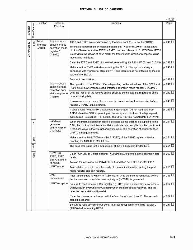
APPENDIX D LIST OF CAUTIONS
User’s Manual U16961EJ4V0UD 491
(16/26)
Cha
pter
Cla
ssifi
catio
n Function Details of Function
Cautions Page
TXE0 and RXE0 are synchronized by the base clock (fXCLK0) set by BRGC0.
To enable transmission or reception again, set TXE0 or RXE0 to 1 at least two clocks of base clock after TXE0 or RXE0 has been cleared to 0. If TXE0 or RXE0 is set within two clocks of base clock, the transmission circuit or reception circuit may not be initialized.
p. 248
Clear the TXE0 and RXE0 bits to 0 before rewriting the PS01, PS00, and CL0 bits. p. 248
Make sure that TXE0 = 0 when rewriting the SL0 bit. Reception is always performed with “number of stop bits = 1”, and therefore, is not affected by the set value of the SL0 bit.
p. 248
Asynchronous serial interface operation mode register 0 (ASIM0)
Be sure to set bit 0 to 1. p. 248
The operation of the PE0 bit differs depending on the set values of the PS01 and PS00 bits of asynchronous serial interface operation mode register 0 (ASIM0).
p. 249
Only the first bit of the receive data is checked as the stop bit, regardless of the number of stop bits.
p. 249
If an overrun error occurs, the next receive data is not written to receive buffer register 0 (RXB0) but discarded.
p. 249
Sof
t
Asynchronous serial interface reception error status register 0 (ASIS0)
If data is read from ASIS0, a wait cycle is generated. Do not read data from ASIS0 when the CPU is operating on the subsystem clock and the high-speed system clock is stopped. For details, see CHAPTER 30 CAUTIONS FOR WAIT.
p. 249
Har
d When the internal oscillation clock is selected as the clock to be supplied to the CPU, the clock of the internal oscillator is divided and supplied as the count clock. If the base clock is the internal oscillation clock, the operation of serial interface UART0 is not guaranteed.
p. 251
Sof
t Make sure that bit 6 (TXE0) and bit 5 (RXE0) of the ASIM0 register = 0 when rewriting the MDL04 to MDL00 bits.
p. 251
Har
d
Baud rate generator control register 0 (BRGC0)
The baud rate value is the output clock of the 5-bit counter divided by 2. p. 251
POWER0, TXE0, RXE0: Bits 7, 6, and 5 of ASIM0
Clear POWER0 to 0 after clearing TXE0 and RXE0 to 0 to set the operation stop mode.
To start the operation, set POWER0 to 1, and then set TXE0 and RXE0 to 1.
p. 252
UART mode Take relationship with the other party of communication when setting the port mode register and port register.
p. 253
UART transmission
After transmit data is written to TXS0, do not write the next transmit data before the transmission completion interrupt signal (INTST0) is generated.
p. 256
Be sure to read receive buffer register 0 (RXB0) even if a reception error occurs. Otherwise, an overrun error will occur when the next data is received, and the reception error status will persist.
p. 257
Reception is always performed with the “number of stop bits = 1”. The second stop bit is ignored.
p. 257
CH
AP
TER
12
Sof
t
Serial Interface UART0
UART reception
Be sure to read asynchronous serial interface reception error status register 0 (ASIS0) before reading RXB0.
p. 257
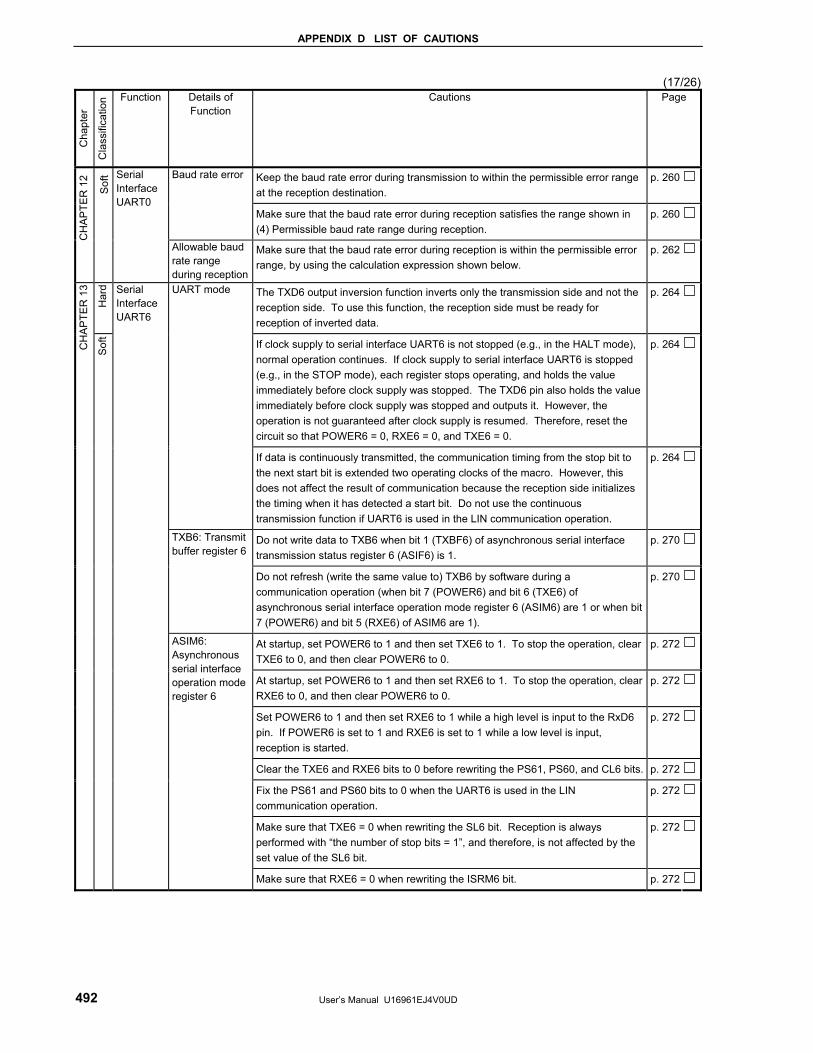
APPENDIX D LIST OF CAUTIONS
User’s Manual U16961EJ4V0UD 492
(17/26) C
hapt
er
Cla
ssifi
catio
n Function Details of Function
Cautions Page
Keep the baud rate error during transmission to within the permissible error range at the reception destination.
p. 260Baud rate error
Make sure that the baud rate error during reception satisfies the range shown in (4) Permissible baud rate range during reception.
p. 260
CH
AP
TER
12
Sof
t Serial Interface UART0
Allowable baud rate range during reception
Make sure that the baud rate error during reception is within the permissible error range, by using the calculation expression shown below.
p. 262
Har
d The TXD6 output inversion function inverts only the transmission side and not the reception side. To use this function, the reception side must be ready for reception of inverted data.
p. 264
If clock supply to serial interface UART6 is not stopped (e.g., in the HALT mode), normal operation continues. If clock supply to serial interface UART6 is stopped (e.g., in the STOP mode), each register stops operating, and holds the value immediately before clock supply was stopped. The TXD6 pin also holds the value immediately before clock supply was stopped and outputs it. However, the operation is not guaranteed after clock supply is resumed. Therefore, reset the circuit so that POWER6 = 0, RXE6 = 0, and TXE6 = 0.
p. 264
UART mode
If data is continuously transmitted, the communication timing from the stop bit to the next start bit is extended two operating clocks of the macro. However, this does not affect the result of communication because the reception side initializes the timing when it has detected a start bit. Do not use the continuous transmission function if UART6 is used in the LIN communication operation.
p. 264
Do not write data to TXB6 when bit 1 (TXBF6) of asynchronous serial interface transmission status register 6 (ASIF6) is 1.
p. 270TXB6: Transmit buffer register 6
Do not refresh (write the same value to) TXB6 by software during a communication operation (when bit 7 (POWER6) and bit 6 (TXE6) of asynchronous serial interface operation mode register 6 (ASIM6) are 1 or when bit 7 (POWER6) and bit 5 (RXE6) of ASIM6 are 1).
p. 270
At startup, set POWER6 to 1 and then set TXE6 to 1. To stop the operation, clear TXE6 to 0, and then clear POWER6 to 0.
p. 272
At startup, set POWER6 to 1 and then set RXE6 to 1. To stop the operation, clear RXE6 to 0, and then clear POWER6 to 0.
p. 272
Set POWER6 to 1 and then set RXE6 to 1 while a high level is input to the RxD6 pin. If POWER6 is set to 1 and RXE6 is set to 1 while a low level is input, reception is started.
p. 272
Clear the TXE6 and RXE6 bits to 0 before rewriting the PS61, PS60, and CL6 bits. p. 272
Fix the PS61 and PS60 bits to 0 when the UART6 is used in the LIN communication operation.
p. 272
Make sure that TXE6 = 0 when rewriting the SL6 bit. Reception is always performed with “the number of stop bits = 1”, and therefore, is not affected by the set value of the SL6 bit.
p. 272
CH
AP
TER
13
Sof
t
Serial Interface UART6
ASIM6: Asynchronous serial interface operation mode register 6
Make sure that RXE6 = 0 when rewriting the ISRM6 bit. p. 272

APPENDIX D LIST OF CAUTIONS
User’s Manual U16961EJ4V0UD 493
(18/26)
Cha
pter
Cla
ssifi
catio
n Function Details of Function
Cautions Page
The operation of the PE6 bit differs depending on the set values of the PS61 and PS60 bits of asynchronous serial interface operation mode register 6 (ASIM6).
p. 273
The first bit of the receive data is checked as the stop bit, regardless of the number of stop bits.
p. 273
If an overrun error occurs, the next receive data is not written to receive buffer register 6 (RXB6) but discarded.
p. 273
ASIS6: Asynchronous serial interface reception error status register 6
If data is read from ASIS6, a wait cycle is generated. Do not read data from ASIS6 when the CPU is operating on the subsystem clock and the high-speed system clock is stopped. For details, see CHAPTER 30 CAUTIONS FOR WAIT.
p. 273
To transmit data continuously, write the first transmit data (first byte) to the TXB6 register. After that, be sure to check that the TXBF6 flag is “0”. If so, write the next transmit data (second byte) to the TXB6 register. If data is written to the TXB6 register while the TXBF6 flag is “1”, the transmit data cannot be guaranteed.
p. 274
Sof
t
ASIF6: Asynchronous serial interface transmission status register 6
To initialize the transmission unit upon completion of continuous transmission, be sure to check that the TXSF6 flag is “0” after generation of the transmission completion interrupt, and then execute initialization. If initialization is executed while the TXSF6 flag is “1”, the transmit data cannot be guaranteed.
p. 274
Har
d When the internal oscillation clock is selected as the clock to be supplied to the CPU, the clock of the internal oscillator is divided and supplied as the count clock. If the base clock is the internal oscillation clock, the operation of serial interface UART6 is not guaranteed.
p. 275CKSR6: Clock selection register 6
Make sure POWER6 = 0 when rewriting TPS63 to TPS60. p. 276
Sof
t
Make sure that bit 6 (TXE6) and bit 5 (RXE6) of the ASIM6 register = 0 when rewriting the MDL67 to MDL60 bits.
p. 276
Har
d
BRGC6: Baud rate generator control register 6 The baud rate is the output clock of the 8-bit counter divided by 2. p. 276
ASICL6 can be refreshed (the same value is written) by software during a communication operation (when bit 7 (POWER6) and bit 6 (TXE6) of ASIM6 = 1 or bit 7 (POWER6) and bit 5 (RXE6) of ASIM6 = 1). Note, however, that communication is started by the refresh operation because bit 6 (SBRT6) of ASICL6 is cleared to 0 when communication is completed (when an interrupt signal is generated). However, do not set both SBRT6 and SBTT6 to 1 by a refresh operation during SBF reception (SBRT6 = 1) or SBF transmission (until INST6 occurs since SBTT6 has been set (1) ), because it may re-trigger SBF reception or SBF transmission.
p. 277
In the case of an SBF reception error, the mode returns to the SBF reception mode. The status of the SBRF6 flag is held (1).
p. 278
Before setting the SBRT6 bit, make sure that bit 7 (POWER6) and bit 5 (RXE6) of ASIM6 = 1. After setting the SBRT6 bit to 1, do not clear it to 0 before SBF reception is completed (before an interrupt request signal is generated).
p. 278
The read value of the SBRT6 bit is always 0. SBRT6 is automatically cleared to 0 after SBF reception has been correctly completed.
p. 278
CH
AP
TER
13
Sof
t
Serial Interface UART6
ASICL6: Asynchronous serial interface control register 6
Before setting the SBTT6 bit to 1, make sure that bit 7 (POWER6) and bit 6 (TXE6) of ASIM6 = 1. After setting the SBTT6 bit to 1, do not clear it to 0 before SBF transmission is completed (before an interrupt request signal is generated).
p. 278
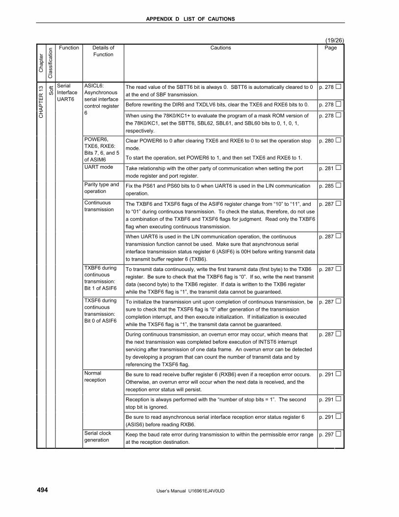
APPENDIX D LIST OF CAUTIONS
User’s Manual U16961EJ4V0UD 494
(19/26) C
hapt
er
Cla
ssifi
catio
n Function Details of Function
Cautions Page
The read value of the SBTT6 bit is always 0. SBTT6 is automatically cleared to 0 at the end of SBF transmission.
p. 278
Before rewriting the DIR6 and TXDLV6 bits, clear the TXE6 and RXE6 bits to 0. p. 278
ASICL6: Asynchronous serial interface control register 6 When using the 78K0/KC1+ to evaluate the program of a mask ROM version of
the 78K0/KC1, set the SBTT6, SBL62, SBL61, and SBL60 bits to 0, 1, 0, 1, respectively.
p. 278
POWER6, TXE6, RXE6: Bits 7, 6, and 5 of ASIM6
Clear POWER6 to 0 after clearing TXE6 and RXE6 to 0 to set the operation stop mode.
To start the operation, set POWER6 to 1, and then set TXE6 and RXE6 to 1.
p. 280
UART mode Take relationship with the other party of communication when setting the port mode register and port register.
p. 281
Parity type and operation
Fix the PS61 and PS60 bits to 0 when UART6 is used in the LIN communication operation.
p. 285
The TXBF6 and TXSF6 flags of the ASIF6 register change from “10” to “11”, and to “01” during continuous transmission. To check the status, therefore, do not use a combination of the TXBF6 and TXSF6 flags for judgment. Read only the TXBF6 flag when executing continuous transmission.
p. 287Continuous transmission
When UART6 is used in the LIN communication operation, the continuous transmission function cannot be used. Make sure that asynchronous serial interface transmission status register 6 (ASIF6) is 00H before writing transmit data to transmit buffer register 6 (TXB6).
p. 287
TXBF6 during continuous transmission: Bit 1 of ASIF6
To transmit data continuously, write the first transmit data (first byte) to the TXB6 register. Be sure to check that the TXBF6 flag is “0”. If so, write the next transmit data (second byte) to the TXB6 register. If data is written to the TXB6 register while the TXBF6 flag is “1”, the transmit data cannot be guaranteed.
p. 287
To initialize the transmission unit upon completion of continuous transmission, be sure to check that the TXSF6 flag is “0” after generation of the transmission completion interrupt, and then execute initialization. If initialization is executed while the TXSF6 flag is “1”, the transmit data cannot be guaranteed.
p. 287TXSF6 during continuous transmission: Bit 0 of ASIF6
During continuous transmission, an overrun error may occur, which means that the next transmission was completed before execution of INTST6 interrupt servicing after transmission of one data frame. An overrun error can be detected by developing a program that can count the number of transmit data and by referencing the TXSF6 flag.
p. 287
Be sure to read receive buffer register 6 (RXB6) even if a reception error occurs. Otherwise, an overrun error will occur when the next data is received, and the reception error status will persist.
p. 291
Reception is always performed with the “number of stop bits = 1”. The second stop bit is ignored.
p. 291
Normal reception
Be sure to read asynchronous serial interface reception error status register 6 (ASIS6) before reading RXB6.
p. 291
CH
AP
TER
13
Sof
t Serial Interface UART6
Serial clock generation
Keep the baud rate error during transmission to within the permissible error range at the reception destination.
p. 297
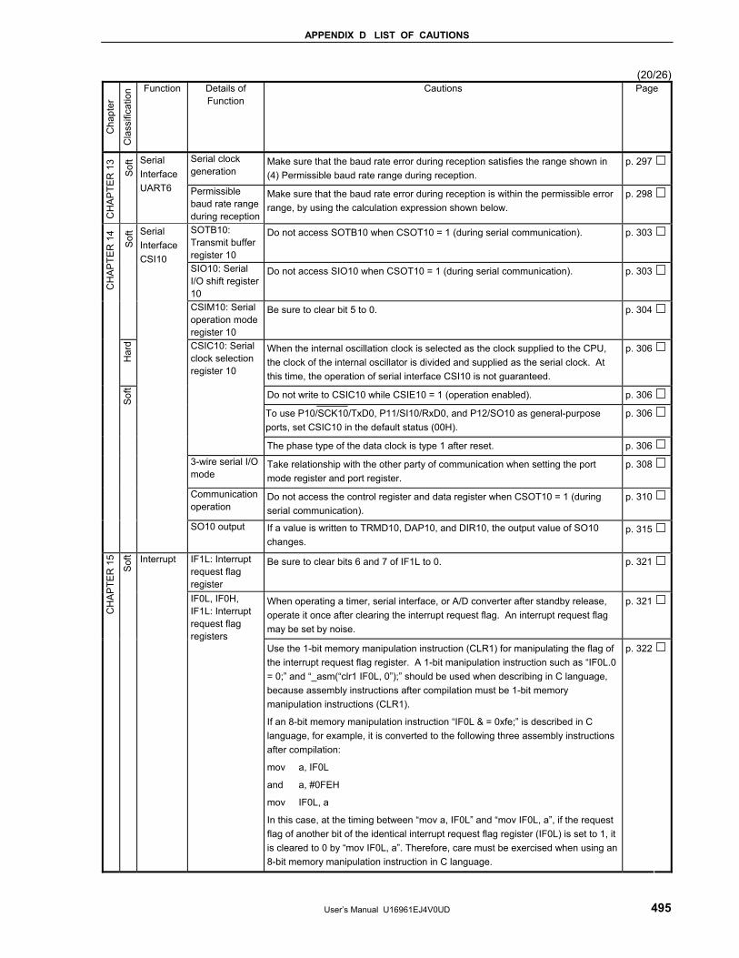
APPENDIX D LIST OF CAUTIONS
User’s Manual U16961EJ4V0UD 495
(20/26)
Cha
pter
Cla
ssifi
catio
n Function Details of Function
Cautions Page
Serial clock generation
Make sure that the baud rate error during reception satisfies the range shown in (4) Permissible baud rate range during reception.
p. 297
CH
AP
TER
13
Sof
t Serial Interface UART6 Permissible
baud rate range during reception
Make sure that the baud rate error during reception is within the permissible error range, by using the calculation expression shown below.
p. 298
SOTB10: Transmit buffer register 10
Do not access SOTB10 when CSOT10 = 1 (during serial communication). p. 303
SIO10: Serial I/O shift register 10
Do not access SIO10 when CSOT10 = 1 (during serial communication). p. 303
Sof
t
CSIM10: Serial operation mode register 10
Be sure to clear bit 5 to 0. p. 304
Har
d When the internal oscillation clock is selected as the clock supplied to the CPU, the clock of the internal oscillator is divided and supplied as the serial clock. At this time, the operation of serial interface CSI10 is not guaranteed.
p. 306
Do not write to CSIC10 while CSIE10 = 1 (operation enabled). p. 306
To use P10/SCK10/TxD0, P11/SI10/RxD0, and P12/SO10 as general-purpose ports, set CSIC10 in the default status (00H).
p. 306
CSIC10: Serial clock selection register 10
The phase type of the data clock is type 1 after reset. p. 3063-wire serial I/O mode
Take relationship with the other party of communication when setting the port mode register and port register.
p. 308
Communication operation
Do not access the control register and data register when CSOT10 = 1 (during serial communication).
p. 310
CH
AP
TER
14
Sof
t
Serial Interface CSI10
SO10 output If a value is written to TRMD10, DAP10, and DIR10, the output value of SO10 changes.
p. 315
IF1L: Interrupt request flag register
Be sure to clear bits 6 and 7 of IF1L to 0. p. 321
When operating a timer, serial interface, or A/D converter after standby release, operate it once after clearing the interrupt request flag. An interrupt request flag may be set by noise.
p. 321
CH
AP
TER
15
Sof
t Interrupt
IF0L, IF0H, IF1L: Interrupt request flag registers
Use the 1-bit memory manipulation instruction (CLR1) for manipulating the flag of the interrupt request flag register. A 1-bit manipulation instruction such as “IF0L.0 = 0;” and “_asm(“clr1 IF0L, 0”);” should be used when describing in C language, because assembly instructions after compilation must be 1-bit memory manipulation instructions (CLR1).
If an 8-bit memory manipulation instruction “IF0L & = 0xfe;” is described in C language, for example, it is converted to the following three assembly instructions after compilation:
mov a, IF0L
and a, #0FEH
mov IF0L, a
In this case, at the timing between “mov a, IF0L” and “mov IF0L, a”, if the request flag of another bit of the identical interrupt request flag register (IF0L) is set to 1, it is cleared to 0 by “mov IF0L, a”. Therefore, care must be exercised when using an 8-bit memory manipulation instruction in C language.
p. 322
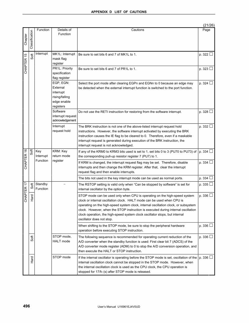
APPENDIX D LIST OF CAUTIONS
User’s Manual U16961EJ4V0UD 496
(21/26) C
hapt
er
Cla
ssifi
catio
n Function Details of Function
Cautions Page
MK1L: Interrupt mask flag register
Be sure to set bits 6 and 7 of MK1L to 1. p. 322
PR1L: Priority specification flag register
Be sure to set bits 6 and 7 of PR1L to 1. p. 323
EGP, EGN: External interrupt rising/falling edge enable registers
Select the port mode after clearing EGPn and EGNn to 0 because an edge may be detected when the external interrupt function is switched to the port function.
p. 324
Software interrupt request acknowledgement
Do not use the RETI instruction for restoring from the software interrupt. p. 328
CH
AP
TER
15
Sof
t Interrupt
Interrupt request hold
The BRK instruction is not one of the above-listed interrupt request hold instructions. However, the software interrupt activated by executing the BRK instruction causes the IE flag to be cleared to 0. Therefore, even if a maskable interrupt request is generated during execution of the BRK instruction, the interrupt request is not acknowledged.
p. 332
If any of the KRM0 to KRM3 bits used is set to 1, set bits 0 to 3 (PU70 to PU73) of the corresponding pull-up resistor register 7 (PU7) to 1.
p. 334
If KRM is changed, the interrupt request flag may be set. Therefore, disable interrupts and then change the KRM register. After that, clear the interrupt request flag and then enable interrupts.
p. 334
CH
AP
TER
16
Sof
t Key Interrupt Function
KRM: Key return mode register
The bits not used in the key interrupt mode can be used as normal ports. p. 334
Sof
t The RSTOP setting is valid only when “Can be stopped by software” is set for internal oscillator by the option byte.
p. 335
STOP mode can be used only when CPU is operating on the high-speed system clock or internal oscillation clock. HALT mode can be used when CPU is operating on the high-speed system clock, internal oscillation clock, or subsystem clock. However, when the STOP instruction is executed during internal oscillation clock operation, the high-speed system clock oscillator stops, but internal oscillator does not stop.
p. 336
Har
d
−
When shifting to the STOP mode, be sure to stop the peripheral hardware operation before executing STOP instruction.
p. 336
Sof
t STOP mode, HALT mode
The following sequence is recommended for operating current reduction of the A/D converter when the standby function is used: First clear bit 7 (ADCS) of the A/D converter mode register (ADM) to 0 to stop the A/D conversion operation, and then execute the HALT or STOP instruction.
p. 336
CH
AP
TER
17
Har
d
Standby Function
STOP mode If the internal oscillator is operating before the STOP mode is set, oscillation of the internal oscillation clock cannot be stopped in the STOP mode. However, when the internal oscillation clock is used as the CPU clock, the CPU operation is stopped for 17/fR (s) after STOP mode is released.
p. 336
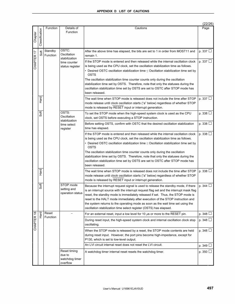
APPENDIX D LIST OF CAUTIONS
User’s Manual U16961EJ4V0UD 497
(22/26)
Cha
pter
Cla
ssifi
catio
n Function Details of Function
Cautions Page
After the above time has elapsed, the bits are set to 1 in order from MOST11 and remain 1.
p. 337
Sof
t
If the STOP mode is entered and then released while the internal oscillation clock is being used as the CPU clock, set the oscillation stabilization time as follows. • Desired OSTC oscillation stabilization time ≤ Oscillation stabilization time set by
OSTS The oscillation stabilization time counter counts only during the oscillation stabilization time set by OSTS. Therefore, note that only the statuses during the oscillation stabilization time set by OSTS are set to OSTC after STOP mode has been released.
p. 337
Har
d
OSTC: Oscillation stabilization time counter status register
The wait time when STOP mode is released does not include the time after STOP mode release until clock oscillation starts (“a” below) regardless of whether STOP mode is released by RESET input or interrupt generation.
p. 337
To set the STOP mode when the high-speed system clock is used as the CPU clock, set OSTS before executing a STOP instruction.
p. 338
Before setting OSTS, confirm with OSTC that the desired oscillation stabilization time has elapsed.
p. 338
Sof
t
If the STOP mode is entered and then released while the internal oscillation clock is being used as the CPU clock, set the oscillation stabilization time as follows. • Desired OSTC oscillation stabilization time ≤ Oscillation stabilization time set by
OSTS The oscillation stabilization time counter counts only during the oscillation stabilization time set by OSTS. Therefore, note that only the statuses during the oscillation stabilization time set by OSTS are set to OSTC after STOP mode has been released.
p. 338
Har
d
OSTS: Oscillation stabilization time select register
The wait time when STOP mode is released does not include the time after STOP mode release until clock oscillation starts (“a” below) regardless of whether STOP mode is released by RESET input or interrupt generation.
p. 338
CH
AP
TER
17
Sof
t
Standby Function
STOP mode setting and operation status
Because the interrupt request signal is used to release the standby mode, if there is an interrupt source with the interrupt request flag set and the interrupt mask flag reset, the standby mode is immediately released if set. Thus, the STOP mode is reset to the HALT mode immediately after execution of the STOP instruction and the system returns to the operating mode as soon as the wait time set using the oscillation stabilization time select register (OSTS) has elapsed.
p. 344
For an external reset, input a low level for 10 μs or more to the RESET pin. p. 348
During reset input, the high-speed system clock and internal oscillation clock stop oscillating.
p. 348
When the STOP mode is released by a reset, the STOP mode contents are held during reset input. However, the port pins become high-impedance, except for P130, which is set to low-level output.
p. 348
−
An LVI circuit internal reset does not reset the LVI circuit. p. 349
CH
AP
TER
18
Har
d Reset Function
Reset timing due to watchdog timer overflow
A watchdog timer internal reset resets the watchdog timer. p. 350
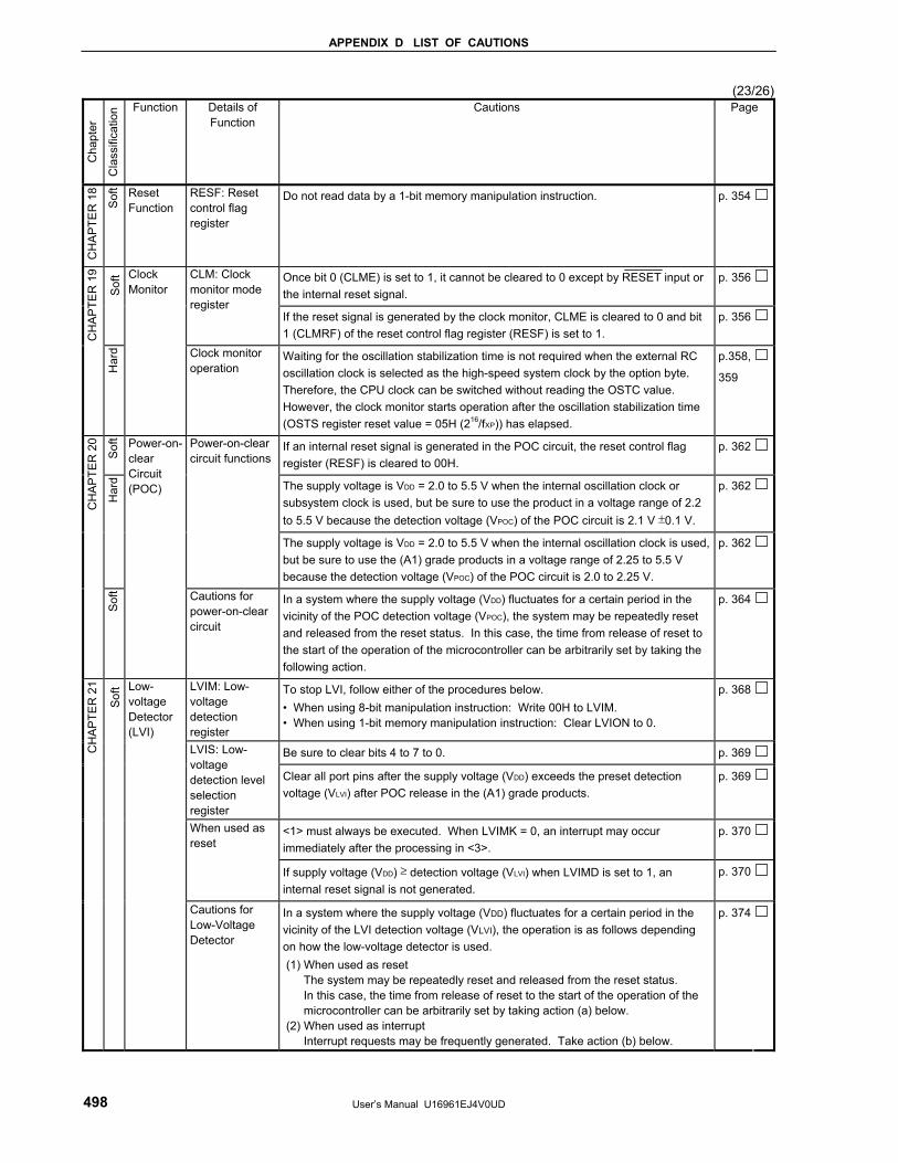
APPENDIX D LIST OF CAUTIONS
User’s Manual U16961EJ4V0UD 498
(23/26) C
hapt
er
Cla
ssifi
catio
n Function Details of Function
Cautions Page C
HA
PTE
R 1
8
Sof
t Reset Function
RESF: Reset control flag register
Do not read data by a 1-bit memory manipulation instruction. p. 354
Once bit 0 (CLME) is set to 1, it cannot be cleared to 0 except by RESET input or the internal reset signal.
p. 356
Sof
t CLM: Clock monitor mode register
If the reset signal is generated by the clock monitor, CLME is cleared to 0 and bit 1 (CLMRF) of the reset control flag register (RESF) is set to 1.
p. 356
CH
AP
TER
19
Har
d
Clock Monitor
Clock monitor operation
Waiting for the oscillation stabilization time is not required when the external RC oscillation clock is selected as the high-speed system clock by the option byte. Therefore, the CPU clock can be switched without reading the OSTC value. However, the clock monitor starts operation after the oscillation stabilization time (OSTS register reset value = 05H (216/fXP)) has elapsed.
p.358,
359
Sof
t
If an internal reset signal is generated in the POC circuit, the reset control flag register (RESF) is cleared to 00H.
p. 362
The supply voltage is VDD = 2.0 to 5.5 V when the internal oscillation clock or subsystem clock is used, but be sure to use the product in a voltage range of 2.2 to 5.5 V because the detection voltage (VPOC) of the POC circuit is 2.1 V ±0.1 V.
p. 362
Har
d
Power-on-clear circuit functions
The supply voltage is VDD = 2.0 to 5.5 V when the internal oscillation clock is used, but be sure to use the (A1) grade products in a voltage range of 2.25 to 5.5 V because the detection voltage (VPOC) of the POC circuit is 2.0 to 2.25 V.
p. 362
CH
AP
TER
20
Sof
t
Power-on-clear Circuit (POC)
Cautions for power-on-clear circuit
In a system where the supply voltage (VDD) fluctuates for a certain period in the vicinity of the POC detection voltage (VPOC), the system may be repeatedly reset and released from the reset status. In this case, the time from release of reset to the start of the operation of the microcontroller can be arbitrarily set by taking the following action.
p. 364
LVIM: Low-voltage detection register
To stop LVI, follow either of the procedures below. • When using 8-bit manipulation instruction: Write 00H to LVIM. • When using 1-bit memory manipulation instruction: Clear LVION to 0.
p. 368
Be sure to clear bits 4 to 7 to 0. p. 369LVIS: Low-voltage detection level selection register
Clear all port pins after the supply voltage (VDD) exceeds the preset detection voltage (VLVI) after POC release in the (A1) grade products.
p. 369
<1> must always be executed. When LVIMK = 0, an interrupt may occur immediately after the processing in <3>.
p. 370When used as reset
If supply voltage (VDD) ≥ detection voltage (VLVI) when LVIMD is set to 1, an internal reset signal is not generated.
p. 370
CH
AP
TER
21
Sof
t Low-voltage Detector (LVI)
Cautions for Low-Voltage Detector
In a system where the supply voltage (VDD) fluctuates for a certain period in the vicinity of the LVI detection voltage (VLVI), the operation is as follows depending on how the low-voltage detector is used. (1) When used as reset
The system may be repeatedly reset and released from the reset status. In this case, the time from release of reset to the start of the operation of the
microcontroller can be arbitrarily set by taking action (a) below. (2) When used as interrupt
Interrupt requests may be frequently generated. Take action (b) below.
p. 374
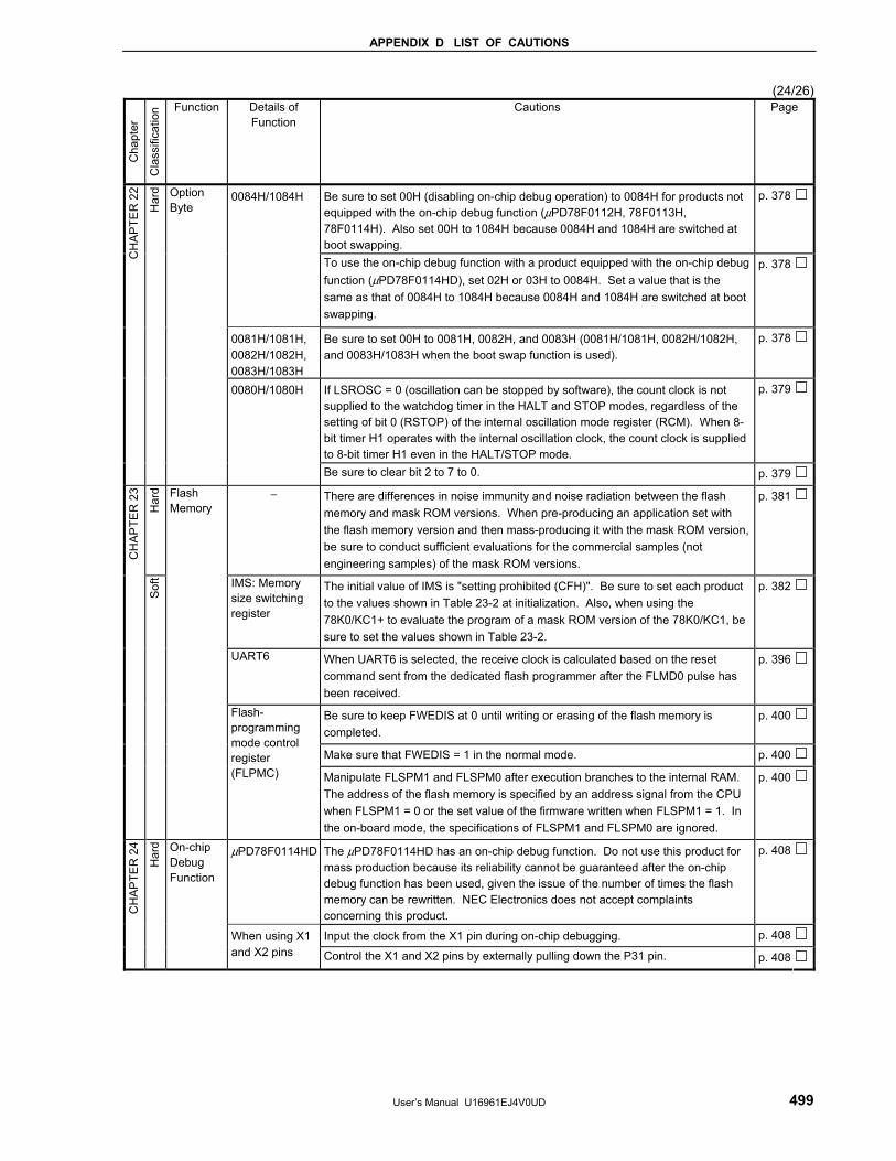
APPENDIX D LIST OF CAUTIONS
User’s Manual U16961EJ4V0UD 499
(24/26)
Cha
pter
Cla
ssifi
catio
n Function Details of Function
Cautions Page
Be sure to set 00H (disabling on-chip debug operation) to 0084H for products not equipped with the on-chip debug function (μPD78F0112H, 78F0113H, 78F0114H). Also set 00H to 1084H because 0084H and 1084H are switched at boot swapping.
p. 3780084H/1084H
To use the on-chip debug function with a product equipped with the on-chip debug function (μPD78F0114HD), set 02H or 03H to 0084H. Set a value that is the same as that of 0084H to 1084H because 0084H and 1084H are switched at boot swapping.
p. 378
0081H/1081H, 0082H/1082H, 0083H/1083H
Be sure to set 00H to 0081H, 0082H, and 0083H (0081H/1081H, 0082H/1082H, and 0083H/1083H when the boot swap function is used).
p. 378
If LSROSC = 0 (oscillation can be stopped by software), the count clock is not supplied to the watchdog timer in the HALT and STOP modes, regardless of the setting of bit 0 (RSTOP) of the internal oscillation mode register (RCM). When 8-bit timer H1 operates with the internal oscillation clock, the count clock is supplied to 8-bit timer H1 even in the HALT/STOP mode.
p. 379
CH
AP
TER
22
Har
d Option Byte
0080H/1080H
Be sure to clear bit 2 to 7 to 0. p. 379
Har
d − There are differences in noise immunity and noise radiation between the flash memory and mask ROM versions. When pre-producing an application set with the flash memory version and then mass-producing it with the mask ROM version, be sure to conduct sufficient evaluations for the commercial samples (not engineering samples) of the mask ROM versions.
p. 381
IMS: Memory size switching register
The initial value of IMS is "setting prohibited (CFH)". Be sure to set each product to the values shown in Table 23-2 at initialization. Also, when using the 78K0/KC1+ to evaluate the program of a mask ROM version of the 78K0/KC1, be sure to set the values shown in Table 23-2.
p. 382
UART6 When UART6 is selected, the receive clock is calculated based on the reset command sent from the dedicated flash programmer after the FLMD0 pulse has been received.
p. 396
Be sure to keep FWEDIS at 0 until writing or erasing of the flash memory is completed.
p. 400
Make sure that FWEDIS = 1 in the normal mode. p. 400
CH
AP
TER
23
Sof
t
Flash Memory
Flash-programming mode control register (FLPMC) Manipulate FLSPM1 and FLSPM0 after execution branches to the internal RAM.
The address of the flash memory is specified by an address signal from the CPU when FLSPM1 = 0 or the set value of the firmware written when FLSPM1 = 1. In the on-board mode, the specifications of FLSPM1 and FLSPM0 are ignored.
p. 400
μPD78F0114HD The μPD78F0114HD has an on-chip debug function. Do not use this product for mass production because its reliability cannot be guaranteed after the on-chip debug function has been used, given the issue of the number of times the flash memory can be rewritten. NEC Electronics does not accept complaints concerning this product.
p. 408
Input the clock from the X1 pin during on-chip debugging. p. 408
CH
AP
TER
24
Har
d On-chip Debug Function
When using X1 and X2 pins Control the X1 and X2 pins by externally pulling down the P31 pin. p. 408
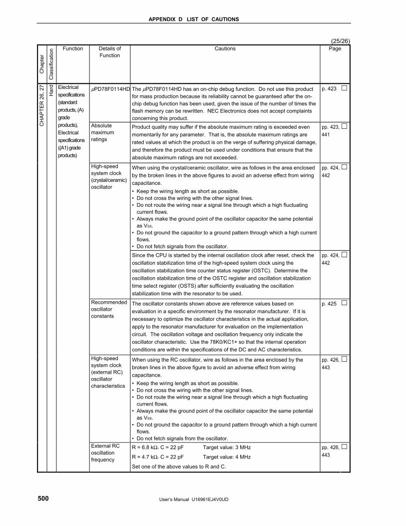
APPENDIX D LIST OF CAUTIONS
User’s Manual U16961EJ4V0UD 500
(25/26) C
hapt
er
Cla
ssifi
catio
n Function Details of Function
Cautions Page
μPD78F0114HD The μPD78F0114HD has an on-chip debug function. Do not use this product for mass production because its reliability cannot be guaranteed after the on-chip debug function has been used, given the issue of the number of times the flash memory can be rewritten. NEC Electronics does not accept complaints concerning this product.
p. 423
Absolute maximum ratings
Product quality may suffer if the absolute maximum rating is exceeded even momentarily for any parameter. That is, the absolute maximum ratings are rated values at which the product is on the verge of suffering physical damage, and therefore the product must be used under conditions that ensure that the absolute maximum ratings are not exceeded.
pp. 423,441
When using the crystal/ceramic oscillator, wire as follows in the area enclosed by the broken lines in the above figures to avoid an adverse effect from wiring capacitance. • Keep the wiring length as short as possible. • Do not cross the wiring with the other signal lines. • Do not route the wiring near a signal line through which a high fluctuating
current flows. • Always make the ground point of the oscillator capacitor the same potential
as VSS. • Do not ground the capacitor to a ground pattern through which a high current
flows. • Do not fetch signals from the oscillator.
pp. 424, 442
High-speed system clock (crystal/ceramic) oscillator
Since the CPU is started by the internal oscillation clock after reset, check the oscillation stabilization time of the high-speed system clock using the oscillation stabilization time counter status register (OSTC). Determine the oscillation stabilization time of the OSTC register and oscillation stabilization time select register (OSTS) after sufficiently evaluating the oscillation stabilization time with the resonator to be used.
pp. 424, 442
Recommended oscillator constants
The oscillator constants shown above are reference values based on evaluation in a specific environment by the resonator manufacturer. If it is necessary to optimize the oscillator characteristics in the actual application, apply to the resonator manufacturer for evaluation on the implementation circuit. The oscillation voltage and oscillation frequency only indicate the oscillator characteristic. Use the 78K0/KC1+ so that the internal operation conditions are within the specifications of the DC and AC characteristics.
p. 425
High-speed system clock (external RC) oscillator characteristics
When using the RC oscillator, wire as follows in the area enclosed by the broken lines in the above figure to avoid an adverse effect from wiring capacitance. • Keep the wiring length as short as possible. • Do not cross the wiring with the other signal lines. • Do not route the wiring near a signal line through which a high fluctuating
current flows. • Always make the ground point of the oscillator capacitor the same potential
as VSS. • Do not ground the capacitor to a ground pattern through which a high current
flows. • Do not fetch signals from the oscillator.
pp. 426, 443
CH
AP
TER
26,
27
Har
d Electrical specifications (standard products, (A) grade products), Electrical specifications ((A1) grade products)
External RC oscillation frequency
R = 6.8 kΩ, C = 22 pF Target value: 3 MHz
R = 4.7 kΩ, C = 22 pF Target value: 4 MHz
Set one of the above values to R and C.
pp. 426, 443
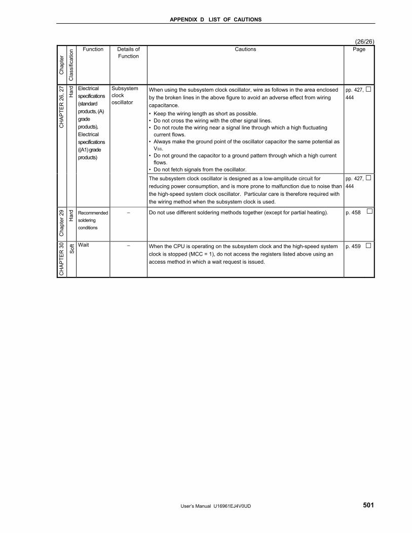
APPENDIX D LIST OF CAUTIONS
User’s Manual U16961EJ4V0UD 501
(26/26)
Cha
pter
Cla
ssifi
catio
n Function Details of Function
Cautions Page
When using the subsystem clock oscillator, wire as follows in the area enclosed by the broken lines in the above figure to avoid an adverse effect from wiring capacitance. • Keep the wiring length as short as possible. • Do not cross the wiring with the other signal lines. • Do not route the wiring near a signal line through which a high fluctuating
current flows. • Always make the ground point of the oscillator capacitor the same potential as
VSS. • Do not ground the capacitor to a ground pattern through which a high current
flows. • Do not fetch signals from the oscillator.
pp. 427, 444
CH
AP
TER
26,
27
Har
d Electrical specifications (standard products, (A) grade products), Electrical specifications ((A1) grade products)
Subsystem clock oscillator
The subsystem clock oscillator is designed as a low-amplitude circuit for reducing power consumption, and is more prone to malfunction due to noise than the high-speed system clock oscillator. Particular care is therefore required with the wiring method when the subsystem clock is used.
pp. 427, 444
Cha
pter
29
Har
d Recommended soldering conditions
− Do not use different soldering methods together (except for partial heating).
p. 458
CH
AP
TER
30
Sof
t Wait − When the CPU is operating on the subsystem clock and the high-speed system clock is stopped (MCC = 1), do not access the registers listed above using an access method in which a wait request is issued.
p. 459
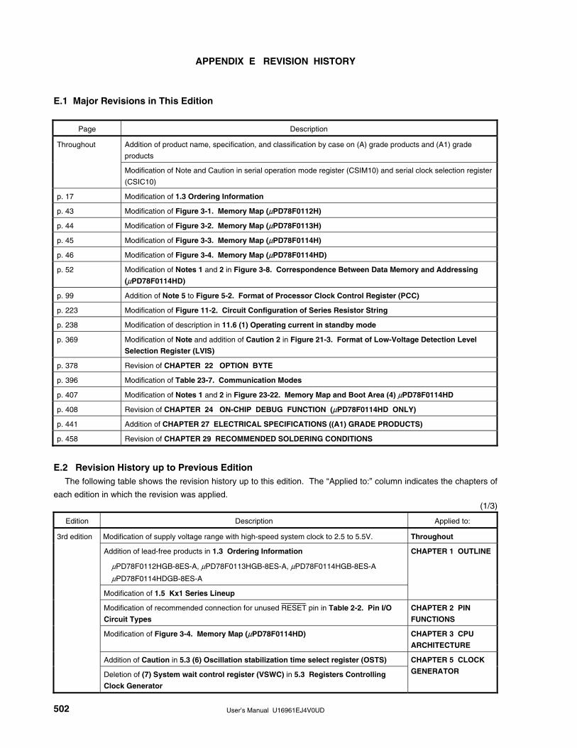
User’s Manual U16961EJ4V0UD 502
APPENDIX E REVISION HISTORY
E.1 Major Revisions in This Edition
Page Description
Addition of product name, specification, and classification by case on (A) grade products and (A1) grade
products
Throughout
Modification of Note and Caution in serial operation mode register (CSIM10) and serial clock selection register
(CSIC10)
p. 17 Modification of 1.3 Ordering Information
p. 43 Modification of Figure 3-1. Memory Map (µPD78F0112H)
p. 44 Modification of Figure 3-2. Memory Map (µPD78F0113H)
p. 45 Modification of Figure 3-3. Memory Map (µPD78F0114H)
p. 46 Modification of Figure 3-4. Memory Map (µPD78F0114HD)
p. 52 Modification of Notes 1 and 2 in Figure 3-8. Correspondence Between Data Memory and Addressing
(µPD78F0114HD)
p. 99 Addition of Note 5 to Figure 5-2. Format of Processor Clock Control Register (PCC)
p. 223 Modification of Figure 11-2. Circuit Configuration of Series Resistor String
p. 238 Modification of description in 11.6 (1) Operating current in standby mode
p. 369 Modification of Note and addition of Caution 2 in Figure 21-3. Format of Low-Voltage Detection Level
Selection Register (LVIS)
p. 378 Revision of CHAPTER 22 OPTION BYTE
p. 396 Modification of Table 23-7. Communication Modes
p. 407 Modification of Notes 1 and 2 in Figure 23-22. Memory Map and Boot Area (4) µPD78F0114HD
p. 408 Revision of CHAPTER 24 ON-CHIP DEBUG FUNCTION (µPD78F0114HD ONLY)
p. 441 Addition of CHAPTER 27 ELECTRICAL SPECIFICATIONS ((A1) GRADE PRODUCTS)
p. 458 Revision of CHAPTER 29 RECOMMENDED SOLDERING CONDITIONS
E.2 Revision History up to Previous Edition
The following table shows the revision history up to this edition. The “Applied to:” column indicates the chapters of
each edition in which the revision was applied. (1/3)
Edition Description Applied to:
Modification of supply voltage range with high-speed system clock to 2.5 to 5.5V. Throughout
Addition of lead-free products in 1.3 Ordering Information
µPD78F0112HGB-8ES-A, µPD78F0113HGB-8ES-A, µPD78F0114HGB-8ES-A
µPD78F0114HDGB-8ES-A
Modification of 1.5 Kx1 Series Lineup
CHAPTER 1 OUTLINE
Modification of recommended connection for unused RESET pin in Table 2-2. Pin I/O
Circuit Types
CHAPTER 2 PIN
FUNCTIONS
Modification of Figure 3-4. Memory Map (µPD78F0114HD) CHAPTER 3 CPU
ARCHITECTURE
Addition of Caution in 5.3 (6) Oscillation stabilization time select register (OSTS)
3rd edition
Deletion of (7) System wait control register (VSWC) in 5.3 Registers Controlling
Clock Generator
CHAPTER 5 CLOCK
GENERATOR
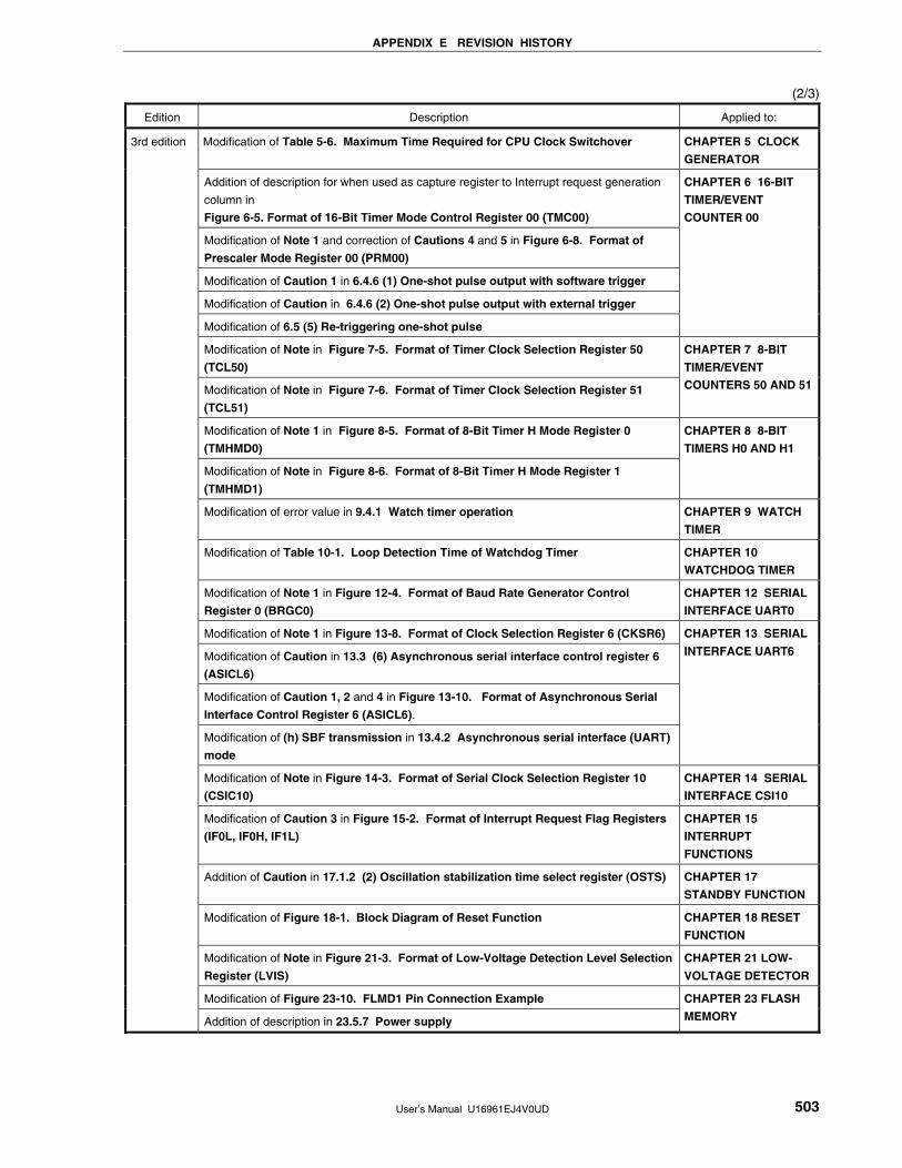
APPENDIX E REVISION HISTORY
User’s Manual U16961EJ4V0UD 503
(2/3)
Edition Description Applied to:
Modification of Table 5-6. Maximum Time Required for CPU Clock Switchover CHAPTER 5 CLOCK
GENERATOR
Addition of description for when used as capture register to Interrupt request generation
column in
Figure 6-5. Format of 16-Bit Timer Mode Control Register 00 (TMC00)
Modification of Note 1 and correction of Cautions 4 and 5 in Figure 6-8. Format of
Prescaler Mode Register 00 (PRM00)
Modification of Caution 1 in 6.4.6 (1) One-shot pulse output with software trigger
Modification of Caution in 6.4.6 (2) One-shot pulse output with external trigger
Modification of 6.5 (5) Re-triggering one-shot pulse
CHAPTER 6 16-BIT
TIMER/EVENT
COUNTER 00
Modification of Note in Figure 7-5. Format of Timer Clock Selection Register 50
(TCL50)
Modification of Note in Figure 7-6. Format of Timer Clock Selection Register 51
(TCL51)
CHAPTER 7 8-BIT
TIMER/EVENT
COUNTERS 50 AND 51
Modification of Note 1 in Figure 8-5. Format of 8-Bit Timer H Mode Register 0
(TMHMD0)
Modification of Note in Figure 8-6. Format of 8-Bit Timer H Mode Register 1
(TMHMD1)
CHAPTER 8 8-BIT
TIMERS H0 AND H1
Modification of error value in 9.4.1 Watch timer operation CHAPTER 9 WATCH
TIMER
Modification of Table 10-1. Loop Detection Time of Watchdog Timer CHAPTER 10
WATCHDOG TIMER
Modification of Note 1 in Figure 12-4. Format of Baud Rate Generator Control
Register 0 (BRGC0)
CHAPTER 12 SERIAL
INTERFACE UART0
Modification of Note 1 in Figure 13-8. Format of Clock Selection Register 6 (CKSR6)
Modification of Caution in 13.3 (6) Asynchronous serial interface control register 6
(ASICL6)
Modification of Caution 1, 2 and 4 in Figure 13-10. Format of Asynchronous Serial
Interface Control Register 6 (ASICL6).
Modification of (h) SBF transmission in 13.4.2 Asynchronous serial interface (UART)
mode
CHAPTER 13 SERIAL
INTERFACE UART6
Modification of Note in Figure 14-3. Format of Serial Clock Selection Register 10
(CSIC10)
CHAPTER 14 SERIAL
INTERFACE CSI10
Modification of Caution 3 in Figure 15-2. Format of Interrupt Request Flag Registers
(IF0L, IF0H, IF1L)
CHAPTER 15
INTERRUPT
FUNCTIONS
Addition of Caution in 17.1.2 (2) Oscillation stabilization time select register (OSTS) CHAPTER 17
STANDBY FUNCTION
Modification of Figure 18-1. Block Diagram of Reset Function CHAPTER 18 RESET
FUNCTION
Modification of Note in Figure 21-3. Format of Low-Voltage Detection Level Selection
Register (LVIS)
CHAPTER 21 LOW-
VOLTAGE DETECTOR
Modification of Figure 23-10. FLMD1 Pin Connection Example
3rd edition
Addition of description in 23.5.7 Power supply
CHAPTER 23 FLASH
MEMORY
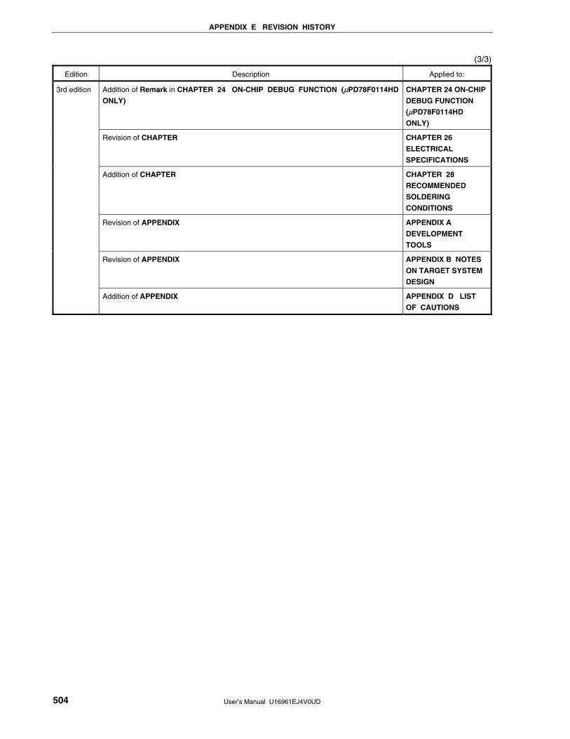
APPENDIX E REVISION HISTORY
User’s Manual U16961EJ4V0UD 504
(3/3)
Edition Description Applied to:
Addition of Remark in CHAPTER 24 ON-CHIP DEBUG FUNCTION (µPD78F0114HD
ONLY)
CHAPTER 24 ON-CHIP
DEBUG FUNCTION
(µPD78F0114HD
ONLY)
Revision of CHAPTER CHAPTER 26
ELECTRICAL
SPECIFICATIONS
Addition of CHAPTER CHAPTER 28
RECOMMENDED
SOLDERING
CONDITIONS
Revision of APPENDIX APPENDIX A
DEVELOPMENT
TOOLS
Revision of APPENDIX APPENDIX B NOTES
ON TARGET SYSTEM
DESIGN
3rd edition
Addition of APPENDIX APPENDIX D LIST
OF CAUTIONS
NEC Electronics Corporation1753, Shimonumabe, Nakahara-ku,Kawasaki, Kanagawa 211-8668, JapanTel: 044-435-5111http://www.necel.com/
[America]
NEC Electronics America, Inc.2880 Scott Blvd.Santa Clara, CA 95050-2554, U.S.A.Tel: 408-588-6000 800-366-9782http://www.am.necel.com/
[Asia & Oceania]
NEC Electronics (China) Co., Ltd7th Floor, Quantum Plaza, No. 27 ZhiChunLu HaidianDistrict, Beijing 100083, P.R.ChinaTel: 010-8235-1155http://www.cn.necel.com/
NEC Electronics Shanghai Ltd.Room 2509-2510, Bank of China Tower,200 Yincheng Road Central, Pudong New Area, Shanghai P.R. China P.C:200120Tel: 021-5888-5400http://www.cn.necel.com/
NEC Electronics Hong Kong Ltd.12/F., Cityplaza 4,12 Taikoo Wan Road, Hong KongTel: 2886-9318http://www.hk.necel.com/
Seoul Branch11F., Samik Lavied’or Bldg., 720-2,Yeoksam-Dong, Kangnam-Ku,Seoul, 135-080, KoreaTel: 02-558-3737
NEC Electronics Taiwan Ltd.7F, No. 363 Fu Shing North RoadTaipei, Taiwan, R. O. C.Tel: 02-8175-9600http://www.tw.necel.com/
NEC Electronics Singapore Pte. Ltd.238A Thomson Road, #12-08 Novena Square, Singapore 307684Tel: 6253-8311http://www.sg.necel.com/
For further information, please contact:
G06.8A
[Europe]
NEC Electronics (Europe) GmbHArcadiastrasse 1040472 Düsseldorf, GermanyTel: 0211-65030http://www.eu.necel.com/
Hanover OfficePodbielskistrasse 166 B30177 HannoverTel: 0 511 33 40 2-0
Munich OfficeWerner-Eckert-Strasse 981829 MünchenTel: 0 89 92 10 03-0
Stuttgart OfficeIndustriestrasse 370565 StuttgartTel: 0 711 99 01 0-0
United Kingdom BranchCygnus House, Sunrise ParkwayLinford Wood, Milton KeynesMK14 6NP, U.K.Tel: 01908-691-133
Succursale Française9, rue Paul Dautier, B.P. 5218078142 Velizy-Villacoublay CédexFranceTel: 01-3067-5800
Sucursal en EspañaJuan Esplandiu, 1528007 Madrid, SpainTel: 091-504-2787
Tyskland FilialTäby CentrumEntrance S (7th floor)18322 Täby, SwedenTel: 08 638 72 00
Filiale ItalianaVia Fabio Filzi, 25/A20124 Milano, ItalyTel: 02-667541
Branch The NetherlandsSteijgerweg 65616 HS EindhovenThe NetherlandsTel: 040 265 40 10
Top Related