


γλώσσες
Σελίδες
Νομικός

1 © Alexis Kwasinski, 2012
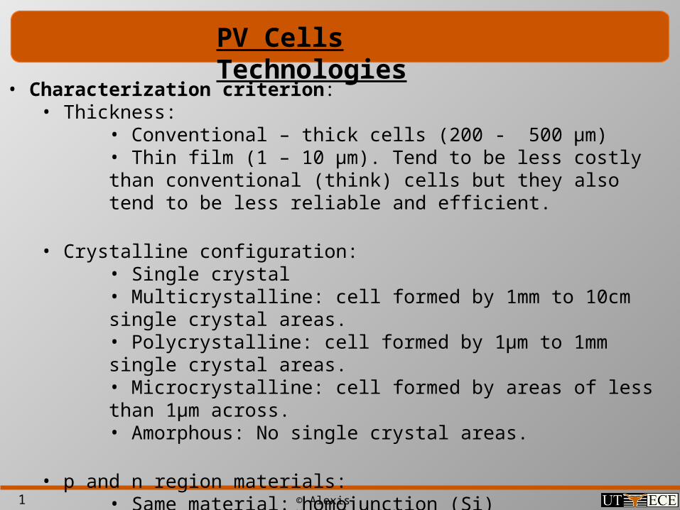
PV Cells Technologies
• Characterization criterion:• Thickness:
• Conventional – thick cells (200 - 500 μm)• Thin film (1 – 10 μm). Tend to be less costly than conventional (think) cells but they also tend to be less reliable and efficient.
• Crystalline configuration:• Single crystal• Multicrystalline: cell formed by 1mm to 10cm single crystal areas.• Polycrystalline: cell formed by 1μm to 1mm single crystal areas.• Microcrystalline: cell formed by areas of less than 1μm across.• Amorphous: No single crystal areas.
• p and n region materials:• Same material: homojunction (Si)• Different material: heterojunction (CdS and CuInSe2)
2 © Alexis Kwasinski, 2012
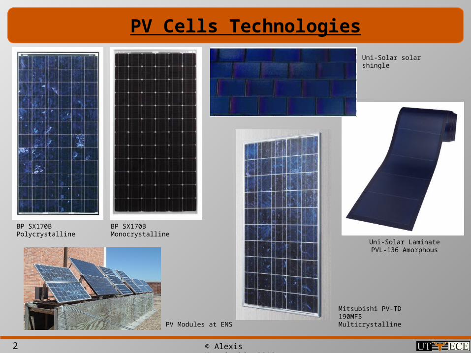
BP SX170B Polycrystalline BP SX170B Monocrystalline
Mitsubishi PV-TD 190MF5 Multicrystalline
Uni-Solar Laminate PVL-136 Amorphous
Uni-Solar solar shingle
PV Modules at ENS
PV Cells Technologies
3 © Alexis Kwasinski, 2012
PV Cells Technologies
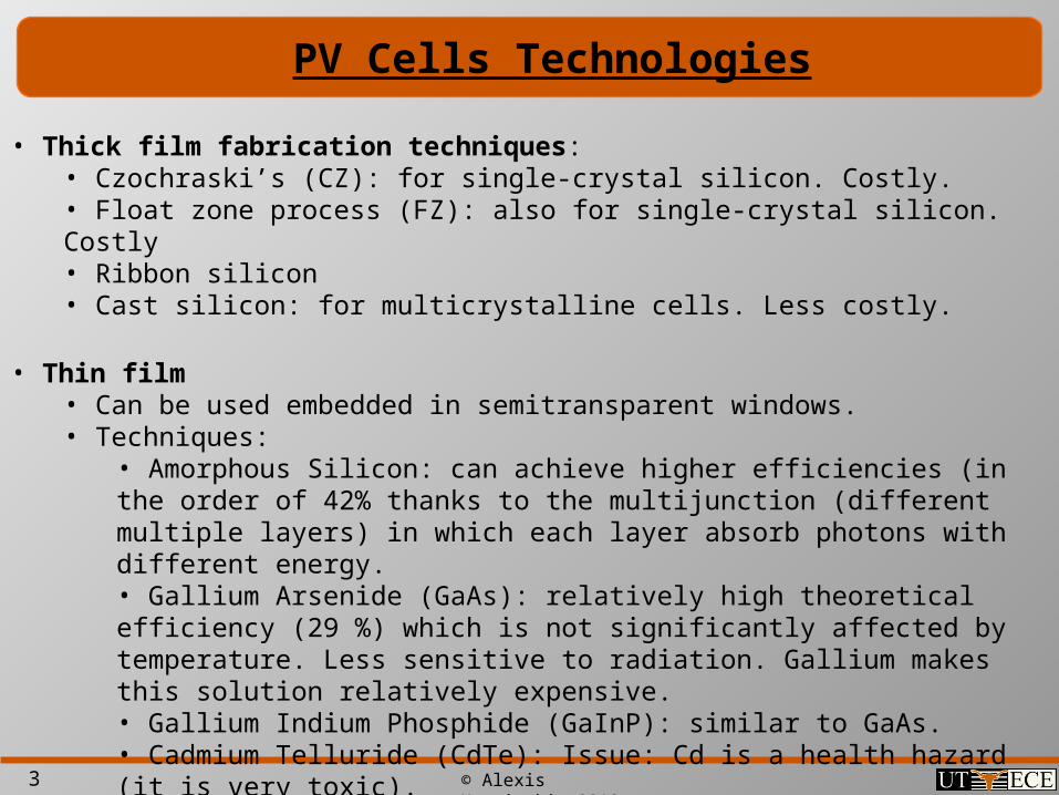
• Thick film fabrication techniques:• Czochraski’s (CZ): for single-crystal silicon. Costly.• Float zone process (FZ): also for single-crystal silicon. Costly• Ribbon silicon• Cast silicon: for multicrystalline cells. Less costly.
• Thin film • Can be used embedded in semitransparent windows.• Techniques:
• Amorphous Silicon: can achieve higher efficiencies (in the order of 42% thanks to the multijunction (different multiple layers) in which each layer absorb photons with different energy.• Gallium Arsenide (GaAs): relatively high theoretical efficiency (29 %) which is not significantly affected by temperature. Less sensitive to radiation. Gallium makes this solution relatively expensive.• Gallium Indium Phosphide (GaInP): similar to GaAs.• Cadmium Telluride (CdTe): Issue: Cd is a health hazard (it is very toxic).• Copper Indium Diselenide (CIS or CuInSe2): relatively good efficiency)• Silicon Nitrade (N4Si3)
4 © Alexis Kwasinski, 2012
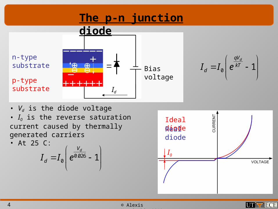
The p-n junction diode
p-type substrate
n-type substrate
Bias voltage
Ideal diodeReal diode
0 1dqV
kTdI I e
Id
• Vd is the diode voltage• I0 is the reverse saturation current caused by thermally generated carriers• At 25 C:
0.0260 1
dV
dI I e
I0
5 © Alexis Kwasinski, 2012
PV Cells physics
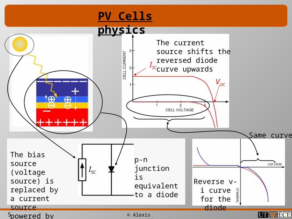
ISC
Reverse v-i curve for the
diode
ISC
VOC
p-n junction is equivalent to a diode
Same curve
The bias source (voltage source) is replaced by a current source powered by the photons
The current source shifts the reversed diode curve upwards

6 © Alexis Kwasinski, 2012
PV Cell steady state characteristic
• From Kirchoff’s current law:
• The open circuit voltage is
0 1dqV
kTPV SC d SCI I I I I e
0
( 0) ln 1SCOC PV
IkTV V I
q I
PV PVP I V
Current
Power
Maximum power point
Pmax 0.7 • Voc • Isc
7 © Alexis Kwasinski, 2012
PV Cell steady state characteristic
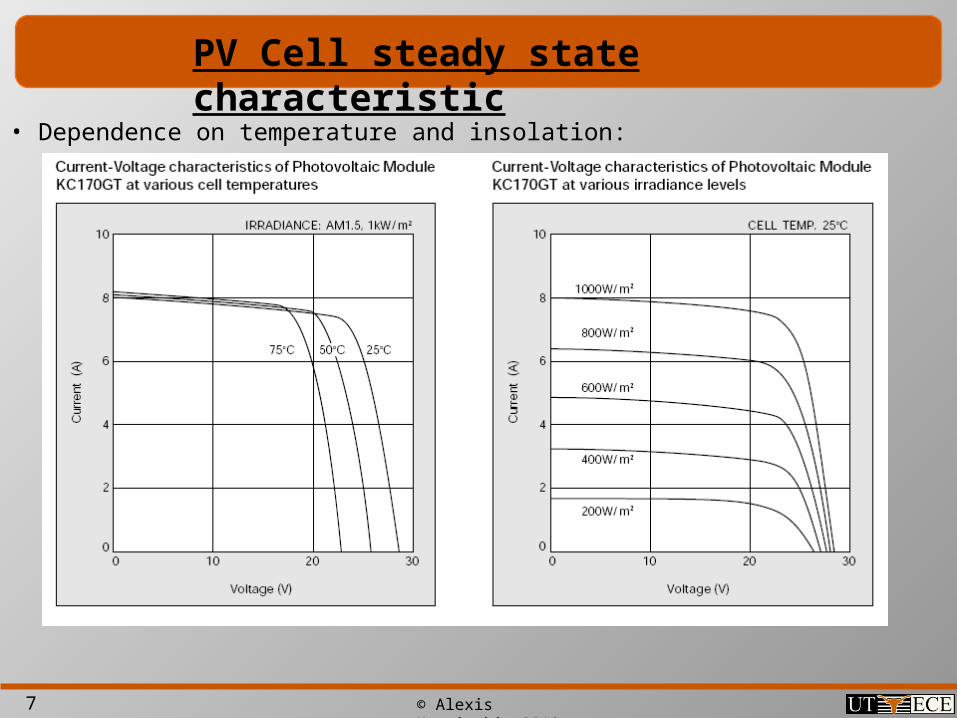
• Dependence on temperature and insolation:
8 © Alexis Kwasinski, 2012
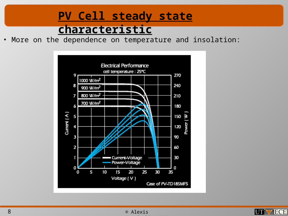
PV Cell steady state characteristic
• More on the dependence on temperature and insolation:
9 © Alexis Kwasinski, 2012
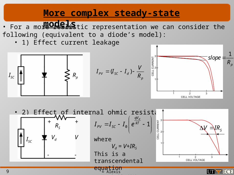
• For a more realistic representation we can consider the following (equivalent to a diode’s model):
• 1) Effect current leakage
• 2) Effect of internal ohmic resistance
More complex steady-state models
ISC
ISC
( )PV SC dp
VI I I
R
1
p
slopeR
SV IR
Rp
RS
Vd
+
V
-
+
-
0 1dqV
kTPV SCI I I e
where Vd = V+IRS
This is a transcendental equation
10 © Alexis Kwasinski, 2012
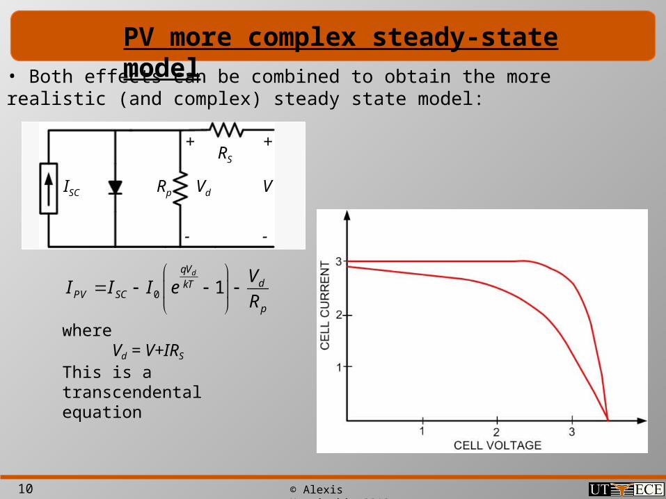
• Both effects can be combined to obtain the more realistic (and complex) steady state model:
PV more complex steady-state model
ISC Rp
RS
Vd V
--
0 1dqV
dkTPV SC
p
VI I I e
R
where Vd = V+IRS
This is a transcendental equation
++
11 © Alexis Kwasinski, 2012
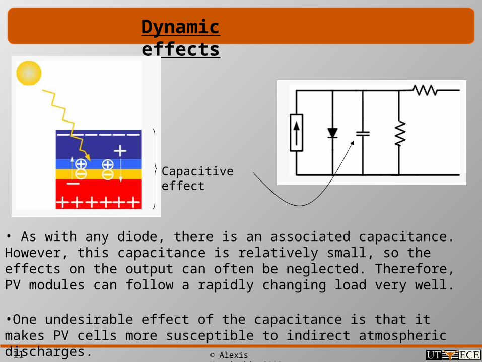
Dynamic effects
Capacitive effect
• As with any diode, there is an associated capacitance. However, this capacitance is relatively small, so the effects on the output can often be neglected. Therefore, PV modules can follow a rapidly changing load very well.
•One undesirable effect of the capacitance is that it makes PV cells more susceptible to indirect atmospheric discharges.
12 © Alexis Kwasinski, 2012
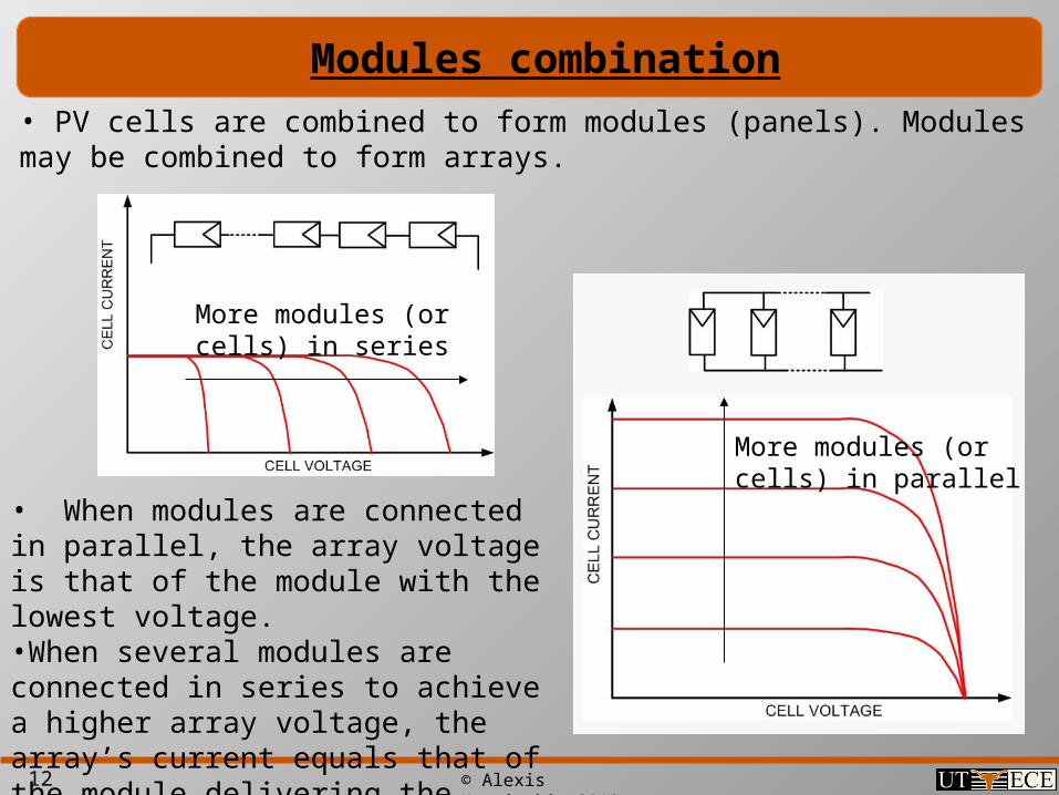
Modules combination• PV cells are combined to form modules (panels). Modules may be combined to form arrays.
More modules (or cells) in series
More modules (or cells) in parallel
• When modules are connected in parallel, the array voltage is that of the module with the lowest voltage.•When several modules are connected in series to achieve a higher array voltage, the array’s current equals that of the module delivering the lowest current.
13 © Alexis Kwasinski, 2012
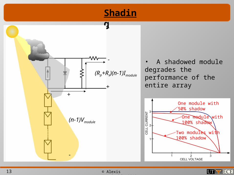
Shading
(n-1)Vmodule
-
++
-
(Rp+Rs)(n-1)Imodule
• A shadowed module degrades the performance of the entire array
One module with 50% shadow
One module with 100% shadow
Two modules with 100% shadow
14 © Alexis Kwasinski, 2012
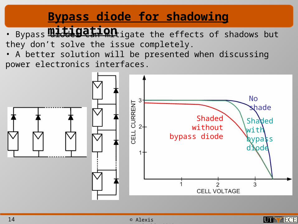
Bypass diode for shadowing mitigation• Bypass diodes can mitigate the effects of shadows but they don’t solve the issue completely.• A better solution will be presented when discussing power electronics interfaces.
No shade
Shaded with bypass diode
Shaded without bypass diode
Top Related