


γλώσσες
Σελίδες
Νομικός

© 2012 Eric Pop, UIUC ECE 340: Semiconductor Electronics 1
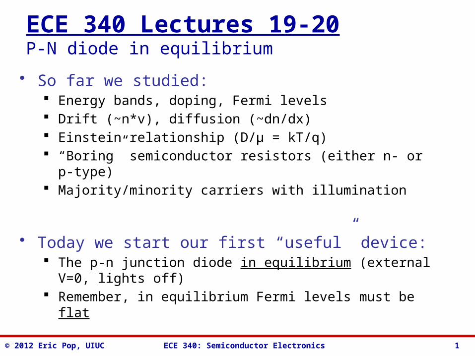
ECE 340 Lectures 19-20P-N diode in equilibrium
• So far we studied: Energy bands, doping, Fermi levels Drift (~n*v), diffusion (~dn/dx) Einstein relationship (D/μ = kT/q) “Boring” semiconductor resistors (either n- or p-type) Majority/minority carriers with illumination
• Today we start our first “useful” device: The p-n junction diode in equilibrium (external V=0, lights off) Remember, in equilibrium Fermi levels must be flat
© 2012 Eric Pop, UIUC ECE 340: Semiconductor Electronics 2
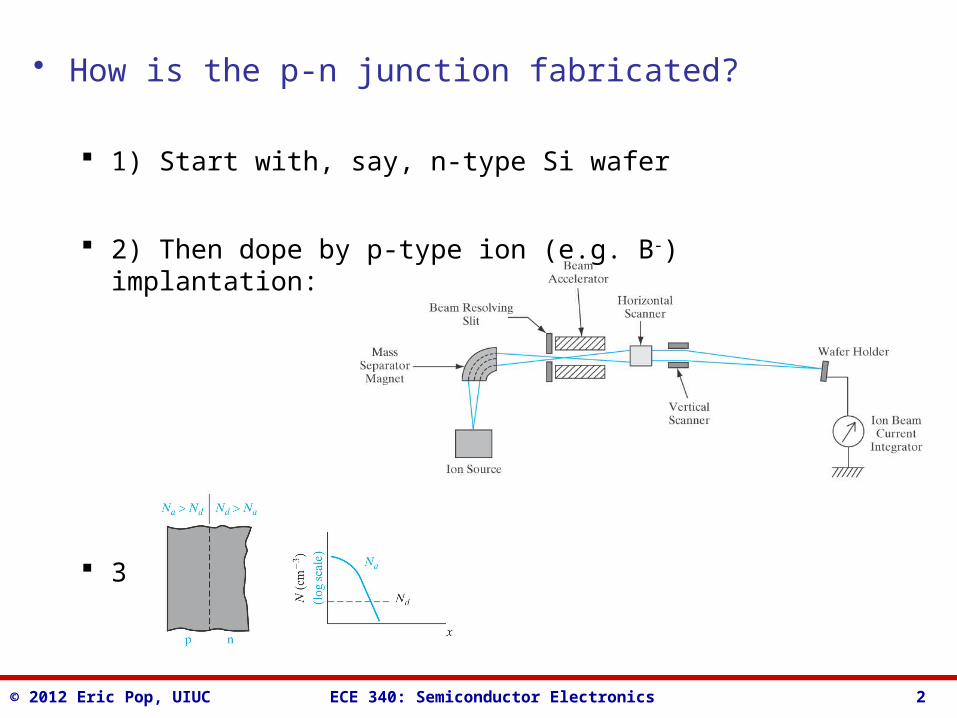
• How is the p-n junction fabricated?
1) Start with, say, n-type Si wafer
2) Then dope by p-type ion (e.g. B-) implantation:
3) Result:
© 2012 Eric Pop, UIUC ECE 340: Semiconductor Electronics 3
• For more details please: Read Streetman book section 5.1 Other books and Wikipedia Take ECE 444!!!
• Back to p-n junction.
• What happens if I bring a p-type and n-type piece of semiconductor together? We already have the tools to analyze this together. Draw isolated band diagrams.
© 2012 Eric Pop, UIUC ECE 340: Semiconductor Electronics 4
• What happens to the (huge!) electron and hole concentrations on either side of the junction, immediately after they are brought together?
• What is required of the Fermi level in equilibrium (why?)
• So draw the p-n band diagram in equilibrium:
© 2012 Eric Pop, UIUC ECE 340: Semiconductor Electronics 5
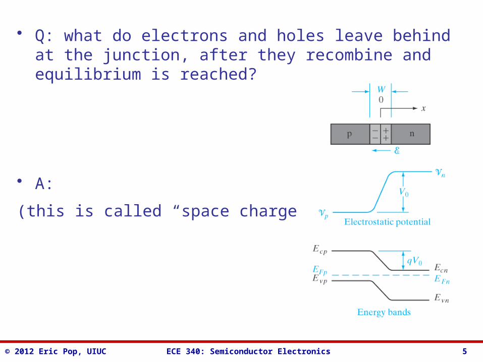
• Q: what do electrons and holes leave behind at the junction, after they recombine and equilibrium is reached?
• A:
(this is called “space charge”)
© 2012 Eric Pop, UIUC ECE 340: Semiconductor Electronics 6
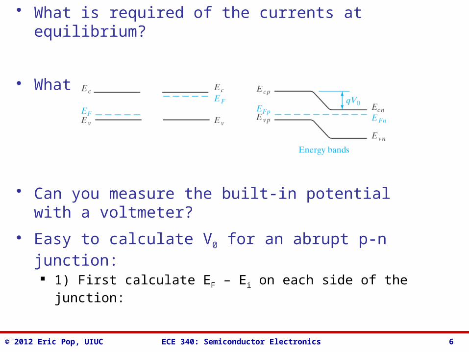
• What is required of the currents at equilibrium?
• What is the built-in potential V0?
• Can you measure the built-in potential with a voltmeter?
• Easy to calculate V0 for an abrupt p-n junction: 1) First calculate EF – Ei on each side of the junction:
2) Notice qV0 = (EFn – Ei) + (Ei – EFp)
© 2012 Eric Pop, UIUC ECE 340: Semiconductor Electronics 7
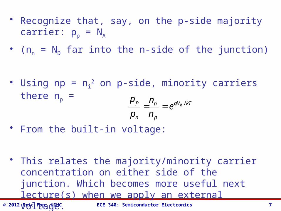
• Recognize that, say, on the p-side majority carrier: pp = NA
• (nn = ND far into the n-side of the junction)
• Using np = ni2 on p-side, minority carriers there np =
• From the built-in voltage:
• This relates the majority/minority carrier concentration on either side of the junction. Which becomes more useful next lecture(s) when we apply an external voltage.
kTqV
p
n
n
p en
n
p
p /0
© 2012 Eric Pop, UIUC ECE 340: Semiconductor Electronics 8
• Ex: (p+)-n junction with NA = 1020 cm-3 and ND = 1015 cm-3. Calculate Fermi levels and built-in potential at equilibrium.
© 2012 Eric Pop, UIUC ECE 340: Semiconductor Electronics 9
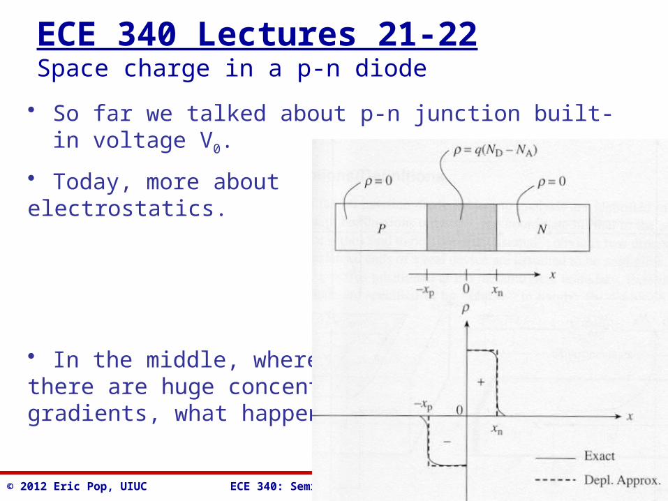
ECE 340 Lectures 21-22Space charge in a p-n diode
• So far we talked about p-n junction built-in voltage V0.
• Today, more aboutelectrostatics.
• In the middle, wherethere are huge concentrationgradients, what happens?

© 2012 Eric Pop, UIUC ECE 340: Semiconductor Electronics 10
• What is left in the middle after the electrons & holes there recombine and are gone?
• Note: we will keep making the depletion approximation which means an ___________________ between the space charge (ND – NA) region and the two quasi-neutral (n and p) regions
• What is the depletion region?
• What is the space charge region (SCR)?
• What are the quasi-neutral regions (QNR)?
• If the SCR width is W = xp + xn, do the two (xp, xn) sides have to be equal? Why or why not?
© 2012 Eric Pop, UIUC ECE 340: Semiconductor Electronics
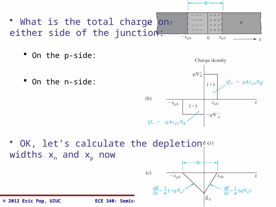
• What is the total charge oneither side of the junction:
On the p-side:
On the n-side:
• OK, let’s calculate the depletionwidths xn and xp now
© 2012 Eric Pop, UIUC ECE 340: Semiconductor Electronics 12
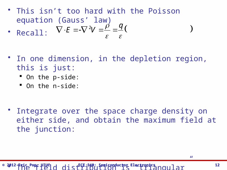
• This isn’t too hard with the Poisson equation (Gauss’ law)
• Recall:
• In one dimension, in the depletion region, this is just: On the p-side: On the n-side:
• Integrate over the space charge density on either side, and obtain the maximum field at the junction:
• The field distribution is “triangular” because the charge distribution is “rectangular” (depletion approximation)
qVE 2
© 2012 Eric Pop, UIUC ECE 340: Semiconductor Electronics 13
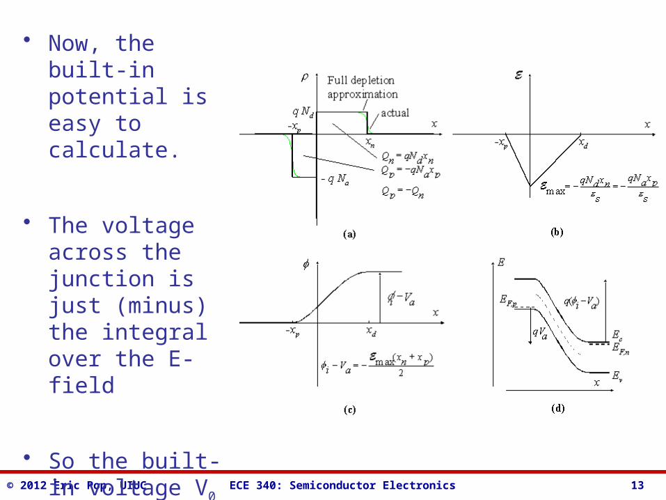
• Now, the built-in potential is easy to calculate.
• The voltage across the junction is just (minus) the integral over the E-field
• So the built-in voltage V0 is the area under the E-field “triangle”
© 2012 Eric Pop, UIUC ECE 340: Semiconductor Electronics 14
• Be careful (a bit):Potential Energy = –q * Voltage Potential
• Although if we use “eV” units for energy (so q = 1 electron) then the two are equivalent numerically (with a minus sign)
• If we use “Joule” units for energy (so q = 1.6 x 10⁻¹⁹ C) then of course you need to be careful multiplying by q to convert from Volts and Joules.
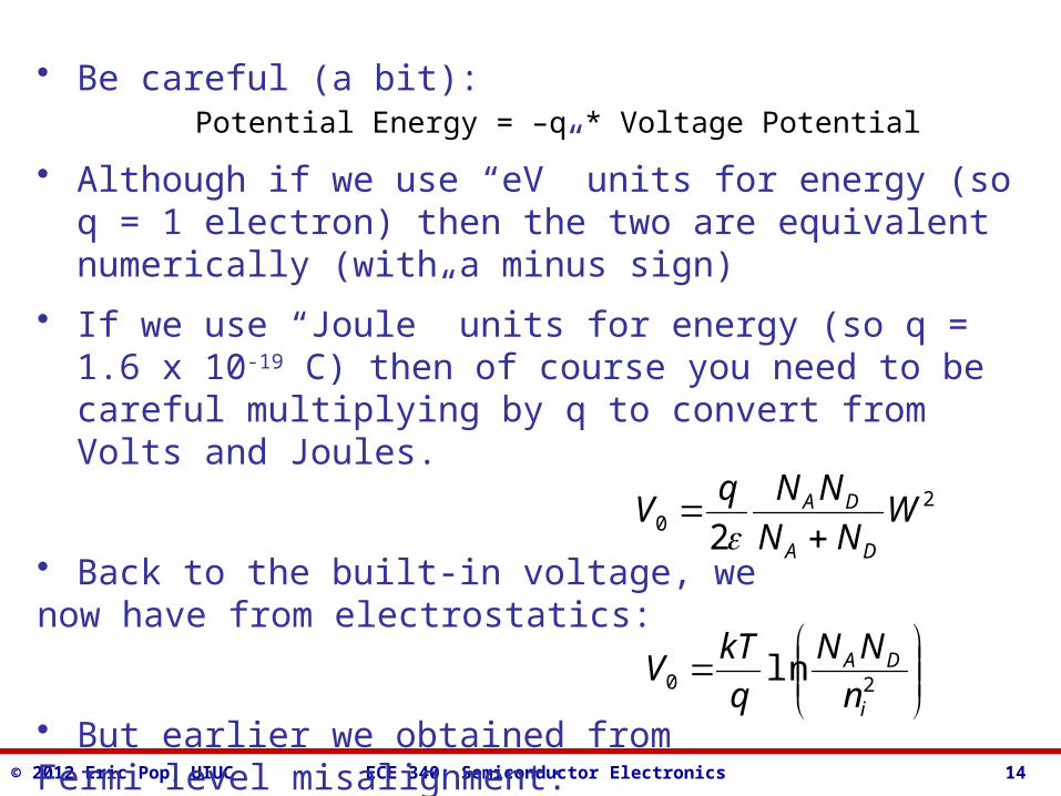
• Back to the built-in voltage, wenow have from electrostatics:
• But earlier we obtained fromFermi level misalignment:
20 2
WNN
NNqV
DA
DA
20 lni
DA
n
NN
q
kTV
© 2012 Eric Pop, UIUC ECE 340: Semiconductor Electronics 15
• Now we can calculate all kinds of things, like the depletion width (W), and the individual depletion regions (xp and xn).
• What if I vary the externally applied voltage? Remember, a positive outside voltage “grabs” the Fermi level on the side it’s
applied on and drags it down. (negative pulls it up). How do we remember this? Think of the simple resistor band diagram, which
way the electric field points (external + to -) and which way the electrons “slide down” or holes “bubble up.”
• A forward bias is + applied to the p-side, which lowers the built-in voltage barrier (V0 – Vfwd) where Vfwd > 0.
• A reverse bias is – applied to the p-side, which increases the built-in voltage barrier (V0 – Vrev) where Vrev < 0.
• Now draw the band diagrams (hint: Fig. 5-13 in the book)
© 2012 Eric Pop, UIUC ECE 340: Semiconductor Electronics 16
• Ex: An abrupt silicon p-n junction has p-side NA = 1016 cm-3, and n-side ND = 5x1016 cm-3. A) What is the built-in voltage. B) How wide is the depletion region with applied V = 0, 0.5 and -2.5 V. C) What is the maximum electric field, and D) the potential across the n-side for these external V’s.
Top Related