
XRT83SL30XRT83SL30 2 SINGLE-CHANNEL T1/E1/J1 SH TRANSCEIVER WITH CLOCK RECOVERY AND JITTER...
76
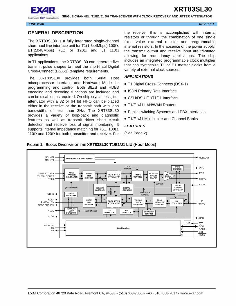
Exar Corporation 48720 Kato Road, Fremont CA, 94538 • (510) 668-7000 • FAX (510) 668-7017 • www.exar.com XRT83SL30 SINGLE-CHANNEL T1/E1/J1 SH TRANSCEIVER WITH CLOCK RECOVERY AND JITTER ATTENUATOR JUNE 2006 REV. 1.0.1 GENERAL DESCRIPTION The XRT83SL30 is a fully integrated single-channel short-haul line interface unit for T1(1.544Mbps) 100Ω, E1(2.048Mbps) 75Ω or 120Ω and J1 110Ω applications. In T1 applications, the XRT83SL30 can generate five transmit pulse shapes to meet the short-haul Digital Cross-Connect (DSX-1) template requirements. The XRT83SL30 provides both Serial Host microprocessor interface and Hardware Mode for programming and control. Both B8ZS and HDB3 encoding and decoding functions are included and can be disabled as required. On-chip crystal-less jitter attenuator with a 32 or 64 bit FIFO can be placed either in the receive or the transmit path with loop bandwidths of less than 3Hz. The XRT83SL30 provides a variety of loop-back and diagnostic features as well as transmit driver short circuit detection and receive loss of signal monitoring. It supports internal impedance matching for 75Ω, 100Ω, 110Ω and 120Ω for both transmitter and receiver. For the receiver this is accomplished with internal resistors or through the combination of one single fixed value external resistor and programmable internal resistors. In the absence of the power supply, the transmit output and receive input are tri-stated allowing for redundancy applications. The chip includes an integrated programmable clock multiplier that can synthesize T1 or E1 master clocks from a variety of external clock sources. APPLICATIONS • T1 Digital Cross-Connects (DSX-1) • ISDN Primary Rate Interface • CSU/DSU E1/T1/J1 Interface • T1/E1/J1 LAN/WAN Routers • Public switching Systems and PBX Interfaces • T1/E1/J1 Multiplexer and Channel Banks FEATURES (See Page 2) FIGURE 1. BLOCK DIAGRAM OF THE XRT83SL30 T1/E1/J1 LIU (HOST MODE) HW/HOST CS INT ICT TPOS / TDATA TNEG / CODES TCLK QRPD RCLK RNEG / LCV RPOS / RDATA NLCD RLOS RTIP RRING MASTER CLOCK SYNTHESIZER QRSS PATTERN GENERATOR DMO TTIP TRING TXON HDB3/ B8ZS ENCODER TX/RX JITTER ATTENUATOR TIMING CONTROL TX FILTER & PULSE SHAPER LINE DRIVER DRIVE MONITOR LOCAL ANALOG LOOPBACK REMOTE LOOPBACK DIGITAL LOOPBACK HDB3/ B8ZS DECODER TX/RX JITTER ATTENUATOR TIMING & DATA RECOVERY PEAK DETECTOR & SLICER QRSS DETECTOR NETWORK LOOP DETECTOR RX EQUALIZER EQUALIZER CONTROL AIS DETECTOR LOS DETECTOR LBO[3:0] LOOPBACK ENABLE JA SELECT NLCD ENABLE QRSS ENABLE SDO SCLK SDI RESET Serial Interface TEST TAOS ENABLE MCLKE1 MCLKT1 MCLKOUT AISD
Transcript of XRT83SL30XRT83SL30 2 SINGLE-CHANNEL T1/E1/J1 SH TRANSCEIVER WITH CLOCK RECOVERY AND JITTER...
XRT83SL30SINGLE-CHANNEL T1/E1/J1 SH TRANSCEIVER WITH CLOCK RECOVERY AND JITTER ATTENUATOR
JUNE 2006 REV. 1.0.1
GENERAL DESCRIPTIONThe XRT83SL30 is a fully integrated single-channel short-haul line interface unit for T1(1.544Mbps) 100Ω, E1(2.048Mbps) 75Ω or 120Ω and J1 110Ω applications.
In T1 applications, the XRT83SL30 can generate five transmit pulse shapes to meet the short-haul Digital Cross-Connect (DSX-1) template requirements.
The XRT83SL30 provides both Serial Host microprocessor interface and Hardware Mode for programming and control. Both B8ZS and HDB3 encoding and decoding functions are included and can be disabled as required. On-chip crystal-less jitter attenuator with a 32 or 64 bit FIFO can be placed either in the receive or the transmit path with loop bandwidths of less than 3Hz. The XRT83SL30 provides a variety of loop-back and diagnostic features as well as transmit driver short circuit detection and receive loss of signal monitoring. It supports internal impedance matching for 75Ω, 100Ω, 110Ω and 120Ω for both transmitter and receiver. For
the receiver this is accomplished with internal resistors or through the combination of one single fixed value external resistor and programmable internal resistors. In the absence of the power supply, the transmit output and receive input are tri-stated allowing for redundancy applications. The chip includes an integrated programmable clock multiplier that can synthesize T1 or E1 master clocks from a variety of external clock sources.
APPLICATIONS
• T1 Digital Cross-Connects (DSX-1)
• ISDN Primary Rate Interface
• CSU/DSU E1/T1/J1 Interface
• T1/E1/J1 LAN/WAN Routers
• Public switching Systems and PBX Interfaces
• T1/E1/J1 Multiplexer and Channel Banks
FEATURES
(See Page 2)
FIGURE 1. BLOCK DIAGRAM OF THE XRT83SL30 T1/E1/J1 LIU (HOST MODE)
HW/HOSTCSINT
ICT
TPOS / TDATATNEG / CODES
TCLK
QRPD
RCLKRNEG / LCV
RPOS / RDATA
NLCD
RLOS
RTIPRRING
MASTER CLOCK SYNTHESIZER
QRSSPATTERN
GENERATOR
DMO
TTIP
TRING
TXON
HDB3/B8ZS
ENCODER
TX/RX JITTERATTENUATOR
TIMINGCONTROL
TX FILTER& PULSESHAPER
LINEDRIVER
DRIVEMONITOR
LOCALANALOG
LOOPBACKREMOTE
LOOPBACKDIGITAL
LOOPBACK
HDB3/B8ZS
DECODER
TX/RX JITTERATTENUATOR
TIMING &DATA
RECOVERY
PEAKDETECTOR& SLICER
QRSSDETECTOR
NETWORKLOOP
DETECTOR
RXEQUALIZER
EQUALIZERCONTROL
AISDETECTOR
LOSDETECTOR
LBO[3:0]
LOOPBACKENABLE
JASE
LEC
T
NLCD ENABLE
QRSS ENABLE
SDOSCLKSDIRESET
Serial Interface
TEST
TAOSENABLE
MCLKE1MCLKT1
MCLKOUT
AISD
Exar Corporation 48720 Kato Road, Fremont CA, 94538 • (510) 668-7000 • FAX (510) 668-7017 • www.exar.com
XRT83SL30 SINGLE-CHANNEL T1/E1/J1 SH TRANSCEIVER WITH CLOCK RECOVERY AND JITTER ATTENUATOR REV. 1.0.1
FEATURES
• Fully integrated single-channel short-haul transceiver for E1,T1 or J1 applications
• Programmable Transmit Pulse Shaper for E1,T1 or J1 short-haul interfaces
• Five fixed transmit pulse settings for T1 short-haul applications plus a fully programmable waveform generator for transmit output pulse shaping
• High receiver interference immunity
• Receive monitor mode handles 0 to 29dB resistive attenuation along with 0 to 6dB of cable attenuation for both T1 and E1 modes
• Supports 75Ω and 120Ω (E1), 100Ω (T1) and 110Ω (J1) applications.
• Internal and/or external impedance matching for 75Ω,100Ω, 110Ω and 120Ω.
• Tri-State transmit output and receive input capability for redundancy applications
• Provides High Impedance for Tx and Rx during power off
• Transmit return loss meets or exceeds ETSI 300 166 standard
• On-chip digital clock recovery circuit for high input jitter tolerance
• Crystal-less digital jitter attenuator with 32-bit or 64-bit FIFO Selectable either in transmit or receive path
• On-chip frequency multiplier generates T1 or E1 Master clocks from variety of external clock sources
• On-chip transmit short-circuit protection and limiting, and driver fail monitor output (DMO)
• Receive loss of signal (RLOS) output
• On-chip HDB3/B8ZS/AMI encoder/decoder
• QRSS pattern generation and detection for testing and monitoring
• Error and Bipolar Violation Insertion and Detection
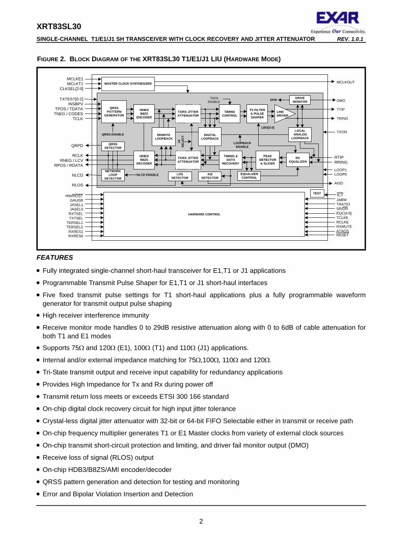
FIGURE 2. BLOCK DIAGRAM OF THE XRT83SL30 T1/E1/J1 LIU (HARDWARE MODE)
HW/HOSTGAUGEJASEL1JASEL0
RXTSELTXTSEL
TERSEL1TERSEL0RXRES1RXRES0
ICT
MCLKE1MCLKT1
CLKSEL[2:0]
TXTEST[0:2]INSBPV
TPOS / TDATATNEG / CODES
TCLK
QRPD
RCLKRNEG / LCV
RPOS / RDATA
NLCD
RLOS
RTIPRRING
MASTER CLOCK SYNTHESIZER
QRSSPATTERN
GENERATOR
DMO
TTIP
TRING
TXON
HDB3/B8ZS
ENCODER
TX/RX JITTERATTENUATOR
TIMINGCONTROL
TX FILTER& PULSESHAPER
LINEDRIVER
LOCALANALOG
LOOPBACKREMOTE
LOOPBACKDIGITAL
LOOPBACK
HDB3/B8ZS
DECODER
TX/RX JITTERATTENUATOR
TIMING &DATA
RECOVERY
PEAKDETECTOR& SLICER
QRSSDETECTOR
NETWORKLOOP
DETECTOR
RXEQUALIZER
EQUALIZERCONTROL
AISDETECTOR
LOSDETECTOR
LBO[3:0]
LOOPBACKENABLE
JASE
LEC
T
NLCD ENABLE
QRSS ENABLE
HARWARE CONTROL
TEST
JABWTRATIOSR/DREQC[4:0]TCLKERCLKERXMUTEATAOS
DRIVEMONITORDFM
MCLKOUT
LOOP1LOOP0
AISD
RESET
TAOSENABLE
2
XRT83SL30REV. 1.0.1 SINGLE-CHANNEL T1/E1/J1 SH TRANSCEIVER WITH CLOCK RECOVERY AND JITTER ATTENUATOR
• Receiver Line Attenuation Indication Output in 1dB steps
• Network Loop-Code Detection for automatic Loop-Back Activation/Deactivation
• Transmit All Ones (TAOS) and In-Band Network Loop Up and Down code generators
• Supports Local Analog, Remote, Digital and Dual Loop-Back Modes
• Meets or exceeds T1 and E1 short-haul network access specifications in ITU G.703, G.775, G.736 and G.823; TR-TSY-000499; ANSI T1.403 and T1.408; ETSI 300-166 and AT&T Pub 62411
• Supports both Hardware and serial Microprocessor interface for programming
• Programmable Interrupt
• Low power dissipation
• Logic inputs accept either 3.3V or 5V levels
• Single +3.3V Supply Operation
• 64 pin TQFP package
• -40°C to +85°C Temperature Range
ORDERING INFORMATIONPART NUMBER PACKAGE OPERATING TEMPERATURE RANGE
XRT83SL30IV 64 Lead TQFP (10 x 10 x 1.4mm) -40°C to +85°C
3
XRT83SL30 SINGLE-CHANNEL T1/E1/J1 SH TRANSCEIVER WITH CLOCK RECOVERY AND JITTER ATTENUATOR REV. 1.0.1
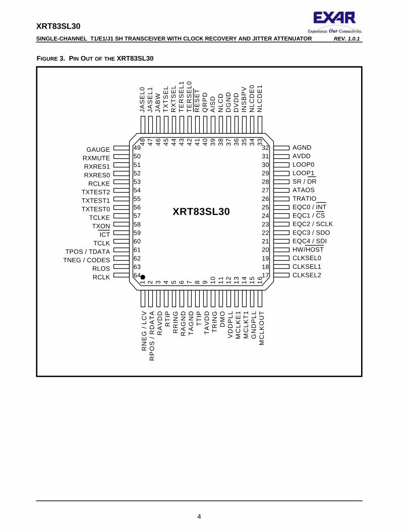
FIGURE 3. PIN OUT OF THE XRT83SL30
XRT83SL30
1 2 3 4 5 6 7 8 9 10 11 12 13 14 15 16
RN
EG
/ LC
VR
PO
S /
RD
AT
AR
AV
DD
RT
IPR
RIN
GR
AG
ND
TA
GN
DT
TIP
TA
VD
DT
RIN
GD
MO
VD
DP
LLM
CLK
E1
MC
LKT
1G
ND
PLL
MC
LKO
UT
AGNDAVDDLOOP0LOOP1SR / DRATAOSTRATIOEQC0 / INTEQC1 / CSEQC2 / SCLKEQC3 / SDOEQC4 / SDIHW/HOSTCLKSEL0CLKSEL1CLKSEL2
JAS
EL0
JAS
EL1
JAB
WT
XT
SE
LR
XT
SE
LT
ER
SE
L1T
ER
SE
L0R
ES
ET
QR
PD
AIS
DN
LCD
DG
ND
DV
DD
INS
BP
VN
LCD
E0
NLC
DE
1
GAUGERXMUTERXRES1RXRES0
RCLKETXTEST2TXTEST1TXTEST0
TCLKETXON
ICTTCLK
TPOS / TDATATNEG / CODES
RLOSRCLK
48 47 46 45 44 43 42 41 40 39 38 37 36 35 34 3332313029282726252423222120191817
49505152535455565758596061626364
4
XRT83SL30REV. 1.0.1 SINGLE-CHANNEL T1/E1/J1 SH TRANSCEIVER WITH CLOCK RECOVERY AND JITTER ATTENUATOR
TABLE OF CONTENTS
GENERAL DESCRIPTION .................................................................................................. 1APPLICATIONS .............................................................................................................................................. 1FEATURES ................................................................................................................................................... 1Figure 1. Block Diagram of the XRT83SL30 T1/E1/J1 LIU (Host Mode) .............................................. 1Figure 2. Block Diagram of the XRT83SL30 T1/E1/J1 LIU (Hardware Mode) ...................................... 2FEATURES ................................................................................................................................................... 2
ORDERING INFORMATION ............................................................................................................... 3Figure 3. Pin Out of the XRT83SL30 ....................................................................................................... 4
TABLE OF CONTENTS ....................................................................................................... IPIN DESCRIPTIONS BY FUNCTION ................................................................................. 5
SERIAL INTERFACE ....................................................................................................................................... 5RECEIVER .................................................................................................................................................... 6TRANSMITTER .............................................................................................................................................. 7JITTER ATTENUATOR .................................................................................................................................... 9CLOCK SYNTHESIZER ................................................................................................................................... 9REDUNDANCY SUPPORT ............................................................................................................................. 11TERMINATIONS ........................................................................................................................................... 11CONTROL FUNCTION ................................................................................................................................... 13ALARM FUNCTION/OTHER ........................................................................................................................... 14POWER AND GROUND ................................................................................................................................. 16
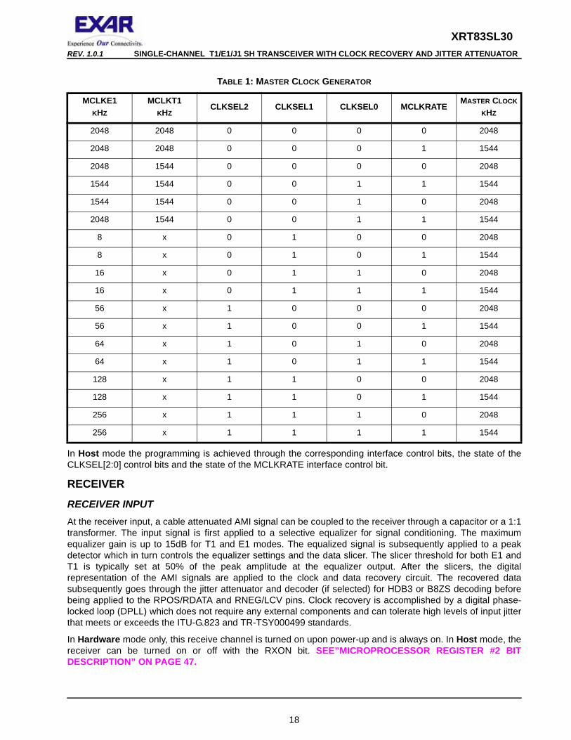
FUNCTIONAL DESCRIPTION .......................................................................................... 17MASTER CLOCK GENERATOR ..................................................................................................................... 17Figure 4. Two Input Clock Source ........................................................................................................ 17Figure 5. One Input Clock Source ........................................................................................................ 17TABLE 1: MASTER CLOCK GENERATOR ..................................................................................................... 18
RECEIVER ......................................................................................................................... 18RECEIVER INPUT ........................................................................................................................................ 18RECEIVE MONITOR MODE ........................................................................................................................... 19RECEIVER LOSS OF SIGNAL (RLOS) ........................................................................................................... 19Figure 6. Simplified Diagram of -15dB T1/E1 Short Haul Mode and RLOS Condition ..................... 19Figure 7. Simplified Diagram of -29dB T1/E1 Gain Mode and RLOS Condition ............................... 20RECEIVE HDB3/B8ZS DECODER ............................................................................................................... 20RECOVERED CLOCK (RCLK) SAMPLING EDGE ............................................................................................ 20Figure 8. Receive Clock and Output Data Timing ............................................................................... 20JITTER ATTENUATOR .................................................................................................................................. 21GAPPED CLOCK (JA MUST BE ENABLED IN THE TRANSMIT PATH) ................................................................ 21TABLE 2: MAXIMUM GAP WIDTH FOR MULTIPLEXER/MAPPER APPLICATIONS .............................................. 21ARBITRARY PULSE GENERATOR ................................................................................................................. 22Figure 9. Arbitrary Pulse Segment Assignment .................................................................................. 22
TRANSMITTER ................................................................................................................. 22DIGITAL DATA FORMAT ............................................................................................................................... 22TRANSMIT CLOCK (TCLK) SAMPLING EDGE ................................................................................................ 22Figure 10. Transmit Clock and Input Data Timing .............................................................................. 23TRANSMIT HDB3/B8ZS ENCODER .............................................................................................................. 23TABLE 3: EXAMPLES OF HDB3 ENCODING ................................................................................................. 23TABLE 4: EXAMPLES OF B8ZS ENCODING ................................................................................................. 23DRIVER FAILURE MONITOR (DMO) ............................................................................................................. 23TRANSMIT PULSE SHAPER & LINE BUILD OUT (LBO) CIRCUIT ...................................................................... 24TABLE 5: RECEIVE EQUALIZER CONTROL AND TRANSMIT LINE BUILD-OUT SETTINGS ................................. 24
TRANSMIT AND RECEIVE TERMINATIONS .................................................................. 25RECEIVER ............................................................................................................................................... 25
Internal Receive Termination Mode ................................................................................................................. 25
I
XRT83SL30 SINGLE-CHANNEL T1/E1/J1 SH TRANSCEIVER WITH CLOCK RECOVERY AND JITTER ATTENUATOR REV. 1.0.1
TABLE 6: RECEIVE TERMINATION CONTROL ................................................................................................ 25Figure 11. Simplified Diagram for the Internal Receive and Transmit Termination Mode ............... 25TABLE 7: RECEIVE TERMINATIONS .............................................................................................................. 26Figure 12. Simplified Diagram for T1 in the External Termination Mode (RXTSEL= 0) .................... 26Figure 13. Simplified Diagram for E1 in External Termination Mode (RXTSEL= 0) .......................... 27TRANSMITTER ........................................................................................................................................ 27
Transmit Termination Mode .............................................................................................................................. 27TABLE 8: TRANSMIT TERMINATION CONTROL .............................................................................................. 27TABLE 9: TERMINATION SELECT CONTROL ................................................................................................. 27
External Transmit Termination Mode ............................................................................................................... 27TABLE 10: TRANSMIT TERMINATION CONTROL ............................................................................................ 28TABLE 11: TRANSMIT TERMINATIONS .......................................................................................................... 28REDUNDANCY APPLICATIONS ............................................................................................................. 28TYPICAL REDUNDANCY SCHEMES ..................................................................................................... 29Figure 14. Simplified Block Diagram of the Transmit Section for 1:1 & 1+1 Redundancy .............. 30Figure 15. Simplified Block Diagram - Receive Section for 1:1 and 1+1 Redundancy .................... 31Figure 16. Simplified Block Diagram - Transmit Section for N+1 Redundancy ................................ 32Figure 17. Simplified Block Diagram - Receive Section for N+1 Redundancy ................................. 33PATTERN TRANSMIT AND DETECT FUNCTION ............................................................................................... 34TABLE 12: PATTERN TRANSMISSION CONTROL ............................................................................................ 34TRANSMIT ALL ONES (TAOS) ..................................................................................................................... 34NETWORK LOOP CODE DETECTION AND TRANSMISSION ............................................................................... 34TABLE 13: LOOP-CODE DETECTION CONTROL ............................................................................................ 35TRANSMIT AND DETECT QUASI-RANDOM SIGNAL SOURCE (TDQRSS) ......................................................... 35LOOP-BACK MODES .................................................................................................................................... 37TABLE 14: LOOP-BACK CONTROL IN HARDWARE MODE ............................................................................... 37TABLE 15: LOOP-BACK CONTROL IN HOST MODE ........................................................................................ 37LOCAL ANALOG LOOP-BACK (ALOOP) ........................................................................................................ 37Figure 18. Local Analog Loop-back signal flow .................................................................................. 37REMOTE LOOP-BACK (RLOOP) .................................................................................................................. 38Figure 19. Remote Loop-back mode with jitter attenuator selected in receive path ....................... 38Figure 20. Remote Loop-back mode with jitter attenuator selected in Transmit path ..................... 38DIGITAL LOOP-BACK (DLOOP) ................................................................................................................... 39Figure 21. Digital Loop-back mode with jitter attenuator selected in Transmit path ....................... 39DUAL LOOP-BACK ...................................................................................................................................... 39Figure 22. Signal flow in Dual loop-back mode ................................................................................... 39
HOST MODE SERIAL INTERFACE OPERATION .......................................................... 40USING THE MICROPROCESSOR SERIAL INTERFACE ...................................................................................... 40Figure 23. Microprocessor Serial Interface Data Structure ................................................................ 41TABLE 16: MICROPROCESSOR REGISTER ADDRESS .................................................................................... 42TABLE 17: MICROPROCESSOR REGISTER BIT MAP ..................................................................................... 42TABLE 18: MICROPROCESSOR REGISTER #0 BIT DESCRIPTION .................................................................... 44TABLE 19: MICROPROCESSOR REGISTER #1 BIT DESCRIPTION .................................................................... 45TABLE 20: MICROPROCESSOR REGISTER #2 BIT DESCRIPTION .................................................................... 47TABLE 21: MICROPROCESSOR REGISTER #3 BIT DESCRIPTION .................................................................... 49TABLE 22: MICROPROCESSOR REGISTER #4 BIT DESCRIPTION .................................................................... 51TABLE 23: MICROPROCESSOR REGISTER #5 BIT DESCRIPTION .................................................................... 52TABLE 24: MICROPROCESSOR REGISTER #6 BIT DESCRIPTION .................................................................... 54TABLE 25: MICROPROCESSOR REGISTER #7 BIT DESCRIPTION .................................................................... 55TABLE 26: MICROPROCESSOR REGISTER #8 BIT DESCRIPTION .................................................................... 55TABLE 27: MICROPROCESSOR REGISTER #9 BIT DESCRIPTION .................................................................... 56TABLE 28: MICROPROCESSOR REGISTER #10 BIT DESCRIPTION .................................................................. 56TABLE 29: MICROPROCESSOR REGISTER #11 BIT DESCRIPTION .................................................................. 57TABLE 30: MICROPROCESSOR REGISTER #12 BIT DESCRIPTION .................................................................. 57TABLE 31: MICROPROCESSOR REGISTER #13 BIT DESCRIPTION .................................................................. 58
II
XRT83SL30REV. 1.0.1 SINGLE-CHANNEL T1/E1/J1 SH TRANSCEIVER WITH CLOCK RECOVERY AND JITTER ATTENUATOR
TABLE 32: MICROPROCESSOR REGISTER #14 BIT DESCRIPTION .................................................................. 58TABLE 33: MICROPROCESSOR REGISTER #15 BIT DESCRIPTION .................................................................. 59TABLE 34: MICROPROCESSOR REGISTER #16 BIT DESCRIPTION .................................................................. 60TABLE 35: MICROPROCESSOR REGISTER #17 BIT DESCRIPTION .................................................................. 61TABLE 36: MICROPROCESSOR REGISTER #18 BIT DESCRIPTION .................................................................. 62ELECTRICAL CHARACTERISTICS .................................................................................................................. 64TABLE 37: ABSOLUTE MAXIMUM RATINGS ................................................................................................. 64TABLE 38: DC DIGITAL INPUT AND OUTPUT ELECTRICAL CHARACTERISTICS .............................................. 64TABLE 39: XRT83SL30 POWER CONSUMPTION ........................................................................................ 64TABLE 40: E1 RECEIVER ELECTRICAL CHARACTERISTICS ........................................................................... 65TABLE 41: T1 RECEIVER ELECTRICAL CHARACTERISTICS ........................................................................... 65TABLE 42: E1 TRANSMIT RETURN LOSS REQUIREMENT .............................................................................. 66TABLE 43: E1 TRANSMITTER ELECTRICAL CHARACTERISTICS ..................................................................... 66TABLE 44: T1 TRANSMITTER ELECTRICAL CHARACTERISTICS ..................................................................... 67Figure 24. ITU G.703 Pulse Template ................................................................................................... 67TABLE 45: TRANSMIT PULSE MASK SPECIFICATION .................................................................................... 68Figure 25. DSX-1 Pulse Template (normalized amplitude) ................................................................. 68TABLE 46: DSX1 INTERFACE ISOLATED PULSE MASK AND CORNER POINTS ............................................... 68TABLE 47: AC ELECTRICAL CHARACTERISTICS .......................................................................................... 69Figure 26. Transmit Clock and Input Data Timing .............................................................................. 70Figure 27. Receive Clock and Output Data Timing ............................................................................. 70
PACKAGE DIMENSIONS ................................................................................................. 7164 LEAD THIN QUAD FLAT PACK ............................................................................................ 71(10 X 10 X 1.4 MM TQFP) ............................................................................................................. 71REV. 3.00 ..................................................................................................................................... 71
ORDERING INFORMATION ............................................................................................. 72TABLE 48. ................................................................................................................................................ 72REVISION HISTORY ..................................................................................................................................... 72
III
XRT83SL30 SINGLE-CHANNEL T1/E1/J1 SH TRANSCEIVER WITH CLOCK RECOVERY AND JITTER ATTENUATOR REV. 1.0.1
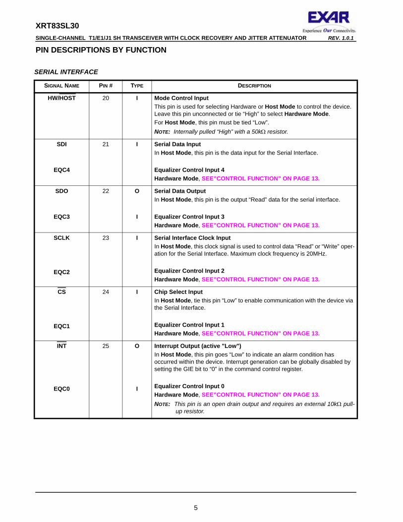
PIN DESCRIPTIONS BY FUNCTION
SERIAL INTERFACE
SIGNAL NAME PIN # TYPE DESCRIPTION
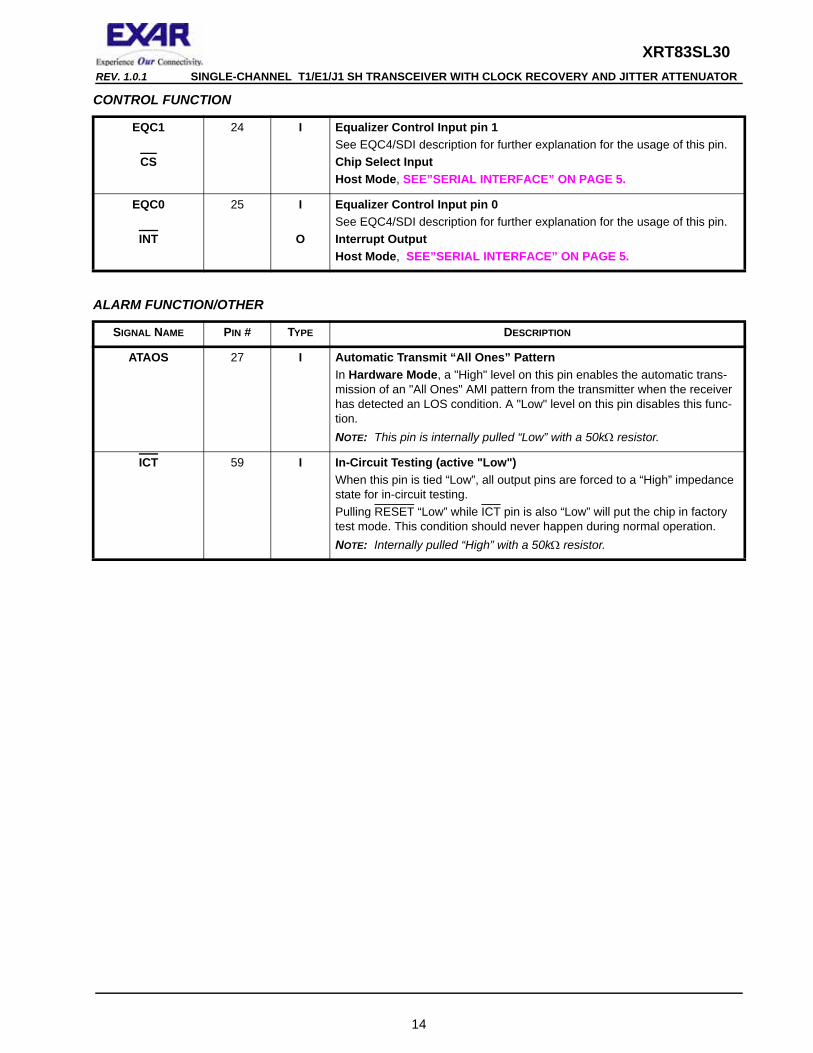
HW/HOST 20 I Mode Control InputThis pin is used for selecting Hardware or Host Mode to control the device. Leave this pin unconnected or tie “High” to select Hardware Mode. For Host Mode, this pin must be tied “Low”.NOTE: Internally pulled “High” with a 50kΩ resistor.
SDI
EQC4
21 I Serial Data InputIn Host Mode, this pin is the data input for the Serial Interface.
Equalizer Control Input 4Hardware Mode, SEE”CONTROL FUNCTION” ON PAGE 13.
SDO
EQC3
22 O
I
Serial Data OutputIn Host Mode, this pin is the output “Read” data for the serial interface.
Equalizer Control Input 3Hardware Mode, SEE”CONTROL FUNCTION” ON PAGE 13.
SCLK
EQC2
23 I Serial Interface Clock InputIn Host Mode, this clock signal is used to control data “Read” or “Write” oper-ation for the Serial Interface. Maximum clock frequency is 20MHz.
Equalizer Control Input 2Hardware Mode, SEE”CONTROL FUNCTION” ON PAGE 13.
CS
EQC1
24 I Chip Select InputIn Host Mode, tie this pin “Low” to enable communication with the device via the Serial Interface.
Equalizer Control Input 1Hardware Mode, SEE”CONTROL FUNCTION” ON PAGE 13.
INT
EQC0
25 O
I
Interrupt Output (active "Low")In Host Mode, this pin goes “Low” to indicate an alarm condition has occurred within the device. Interrupt generation can be globally disabled by setting the GIE bit to “0” in the command control register.
Equalizer Control Input 0Hardware Mode, SEE”CONTROL FUNCTION” ON PAGE 13.NOTE: This pin is an open drain output and requires an external 10kΩ pull-
up resistor.
5
XRT83SL30REV. 1.0.1 SINGLE-CHANNEL T1/E1/J1 SH TRANSCEIVER WITH CLOCK RECOVERY AND JITTER ATTENUATOR
RECEIVER
SIGNAL NAME PIN # TYPE DESCRIPTION
RLOS 63 O Receiver Loss of Signal This signal is asserted ‘High’ for at least one RCLK cycle to indicate loss of signal at the receive input. RLOS will remain “High” for the entire duration of the loss of signal detected by the receiver logic.
RCLK 64 O Receiver Clock Output
RNEG
LCV
1 O Receiver Negative Data Output In dual-rail mode, this signal is the receiver negative-rail output data.
Line Code Violation Output In single-rail mode, this signal goes ‘High’ for one RCLK cycle to indicate a code violation is detected in the received data. If AMI coding is selected, every bipolar violation received will cause this pin to go “High”.
RPOS
RDATA
2 O Receiver Positive Data OutputIn dual-rail mode, this signal is the receive positive-rail output data sent to the Framer.
Receiver NRZ Data OutputIn single-rail mode, this signal is the receive NRZ format output data sent to the Framer.
RTIP 4 I Receiver Differential Tip Positive InputPositive differential receive input from the line.
RRING 5 I Receiver Differential Ring Negative InputNegative differential receive input from the line.
RXMUTE 50 I Receive MutingIn Hardware Mode, connect this pin ‘High’ to mute RPOS and RNEG out-puts to a “Low” state upon receipt of LOS condition to prevent data chatter-ing. Connect this pin to ‘Low’ to disable muting function.NOTE: Internally pulled “Low” with 50kΩ resistor.
RCLKE 53 I Receive Clock EdgeIn Hardware Mode, with this pin set to ‘High’ the output receive data is updated on the falling edge of RCLK. With this pin tied ‘Low’, output data is updated on the rising edge of RCLK.NOTE: Internally pulled “Low” with a 50kΩ resistor.
6
XRT83SL30 SINGLE-CHANNEL T1/E1/J1 SH TRANSCEIVER WITH CLOCK RECOVERY AND JITTER ATTENUATOR REV. 1.0.1
TRANSMITTER
SIGNAL NAME PIN # TYPE DESCRIPTION
TTIP 8 O Transmitter Tip Output Positive differential transmit output to the line.
TRING 10 O Transmitter Ring OutputNegative differential transmit output to the line.
TPOS
TDATA
61 I Transmitter Positive Data InputIn dual-rail mode, this signal is the positive-rail input data for the transmitter.
Transmitter Data InputIn single-rail mode, this pin is used as the NRZ input data for the transmitter.NOTE: Internally pulled “Low” with a 50kΩ resistor.
TNEG
CODES
62 I Transmitter Negative NRZ Data Input In dual-rail mode, this signal is the negative-rail input data for the transmitter. In single-rail mode, this pin can be left unconnected.
Coding SelectIn Hardware Mode and with single-rail mode selected, connecting this pin "Low" enables HDB3 in E1 or B8ZS in T1 encoding and decoding. Connect-ing this pin "High" selects AMI data format.NOTE: Internally pulled “Low” with a 50kΩ resistor.
TCLK 60 I Transmitter Clock Input E1 rate at 2.048MHz ± 50ppmT1 rate at 1.544MHz ± 32ppm
During normal operation, both in Host Mode and Hardware Mode, TCLK is used for sampling input data at TPOS/TDATA and TNEG/CODES while MCLK is used as the timing reference for the transmit pulse shaping circuit.
TCLKE 57 I Transmit Clock EdgeIn Hardware Mode, with this pin set to a "High", transmit input data is sam-pled at the rising edge of TCLK. With this pin tied "Low", input data are sam-pled at the falling edge of TCLK.NOTE: Internally pulled “Low” with a 50kΩ resistor.
TXON 58 I Transmitter Turn On In Hardware Mode, setting this pin "High" turns on the Transmit Section. In this mode, when TXON = “0”, TTIP and TRING driver outputs will be tri-stated.In Host Mode, setting bit 5 (TXONCTL) to “1”, in Register 18 (12h), control of the transmitter output is transferred to the hardware pin TXON.NOTE: Internally pulled "Low" with a 50kΩ resistor.
7
XRT83SL30REV. 1.0.1 SINGLE-CHANNEL T1/E1/J1 SH TRANSCEIVER WITH CLOCK RECOVERY AND JITTER ATTENUATOR
TXTEST2TXTEST1TXTEST0
545556
I Transmit Test Pattern pin 2Transmit Test Pattern pin 1Transmit Test Pattern pin 0In Hardware Mode, TXTEST[2:0] pins are used to generate and transmit test patterns according to the following table:
TAOS (Transmit All Ones): Activating this condition enables the transmis-sion of an All Ones Pattern.TCLK must not be tied "Low". TLUC (Transmit Network Loop-Up Code): Activating this condition enables the Network Loop-Up Code of "00001" to be transmitted to the line. When Network Loop-Up code is being transmitted, the XRT83SL30 will ignore the Automatic Loop-Code detection and Remote Loop-back activation (NLCDE1=”1”, NLCDE0=”1”, if activated) in order to avoid activating Remote Digital Loop-back automatically when the remote terminal responds to the Loop-back request.TLDC (Transmit Network Loop-Down Code): Activating this condition enables the network Loop-Down Code of "001" to be transmitted to the line. TDQRSS (Transmit/Detect Quasi-Random Signal): Setting TXTEST2=”1”, regardless of the state of TXTEST1 and TXTEST0, enables Quasi-Random Signal Source generation and detection. In a T1 system QRSS pattern is a 220-1 pseudo-random bit sequence (PRBS) with no more than 14 consecu-tive zeros. In a E1 system, QRSS is a 215-1 PRBS pattern.When TXTEST2 is “1” and TDQRSS is active, setting TXTEST0 to “1” inverts the polarity of transmitted QRSS pattern. Resetting to "0" sends the QRSS pattern with no inversion.When TXTEST2 is “1” and TDQRSS is active, transitions of TXTEST1 from "0" to "1" results in a bit error to be inserted in the transmitted QRSS pattern. The state of this pin is sampled on the rising edge of TCLK. To ensure the insertion of a bit error, this pin should be reset to a "0" before setting to a "1".When TXTEST2 is “1”, TXTEST1 and TXTEST0 affect the transmitted QRSS bit pattern independently.
TRANSMITTER
SIGNAL NAME PIN # TYPE DESCRIPTION
0 1
1 0
1 1
0 0
0
0
0
1
0 00 Transmit Data
TAOS
TLUC
TLDC
Test PatternTXTEST1 TXTEST0TXTEST2
1 0
1 1
1
1
0 11
TDQRSS
TDQRSS & INVQRSS
TDQRSS & INSBER
TDQRSS & INVQRSS & INS
8
XRT83SL30 SINGLE-CHANNEL T1/E1/J1 SH TRANSCEIVER WITH CLOCK RECOVERY AND JITTER ATTENUATOR REV. 1.0.1
JITTER ATTENUATOR
SIGNAL NAME PIN # TYPE DESCRIPTION
JABW 46 I Jitter Attenuator BandwidthIn Hardware and E1 mode, when JABW=”0” the jitter attenuator bandwidth is 10Hz (normal mode). Setting JABW to “1” selects a 1.5Hz Bandwidth for the Jitter Attenuator and the FIFO length will be automatically set to 64 bits. In T1 mode the Jitter Attenuator Bandwidth is always set to 3Hz, and the state of this pin has no effect on the Bandwidth. See table under JASEL[1:0] pin, below.NOTE: Internally pulled “Low” with a 50kΩ resistor.
JASEL1JASEL0
4748
I Jitter Attenuator select pin 1Jitter Attenuator select pin 0In Hardware Mode, JASEL0, JASEL1 and JABW pins are used to place the jitter attenuator in the transmit path, the receive path or to disable it and set the jitter attenuator bandwidth and FIFO size per the following table.
NOTE: These pins are internally pulled "Low" with 50kΩ resistors.
CLOCK SYNTHESIZER
SIGNAL NAME PIN # TYPE DESCRIPTION
MCLKE1 13 I E1 Master Clock Input This input signal is an independent 2.048MHz clock for E1 system with required accuracy of better than ±50ppm and a duty cycle of 40% to 60%. MCLKE1 is used in the E1 mode. Its function is to provide internal timing for the PLL clock recovery circuit, transmit pulse shaping, jitter attenuator block, reference clock during transmit all ones data and timing reference for the microprocessor in Host Mode operation. MCLKE1 is also input to a programmable frequency synthesizer that under the control of the CLKSEL[2:0] inputs can be used to generate a master clock from an accurate external source. In systems that have only one mas-ter clock source available (E1 or T1), that clock should be connected to both MCLKE1 and MCLKT1 inputs for proper operation.NOTES:
1. See pin descriptions for pins CLKSEL[2:0].2. Internally pulled “Low” with a 50kΩ resistor.
Disabled
Transmit
Receive
Receive
------
32/32
32/32
64/64
------
3
3
3
------
10
10
10
0
0
1
1
0
1
0
1
0
0
0
0
Disabled
Transmit
Receive
Receive
--------
32/64
32/64
64/64
------
3
3
3
------
1.5
1.5
1.5
0
0
1
1
0
1
0
1
1
1
1
1
JA Path JA BW (Hz) FIFO SizeT1/E1JASEL1 JASEL0JABW
T1 E1
9
XRT83SL30REV. 1.0.1 SINGLE-CHANNEL T1/E1/J1 SH TRANSCEIVER WITH CLOCK RECOVERY AND JITTER ATTENUATOR
MCLKT1 14 I T1 Master Clock InputThis signal is an independent 1.544MHz clock for T1 systems with required accuracy of better than ±50ppm and duty cycle of 40% to 60%. MCLKT1 input is used in the T1 mode. NOTES:
1. See MCLKE1 description for further explanation for the usage of this pin.
2. Internally pulled “Low” with a 50kΩ resistor.
MCLKOUT 16 O Synthesized Master Clock OutputThis signal is the output of the Master Clock Synthesizer PLL which is at T1 or E1 rate based on the mode of operation.
CLKSEL2CLKSEL1CLKSEL0
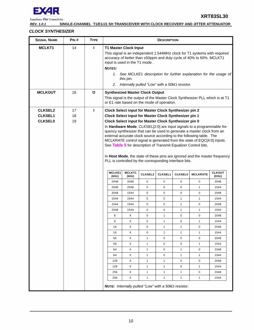
171819
I Clock Select input for Master Clock Synthesizer pin 2Clock Select input for Master Clock Synthesizer pin 1Clock Select input for Master Clock Synthesizer pin 0In Hardware Mode, CLKSEL[2:0] are input signals to a programmable fre-quency synthesizer that can be used to generate a master clock from an external accurate clock source according to the following table. The MCLKRATE control signal is generated from the state of EQC[4:0] inputs. See Table 5 for description of Transmit Equalizer Control bits.
In Host Mode, the state of these pins are ignored and the master frequency PLL is controlled by the corresponding interface bits.
NOTE: Internally pulled "Low" with a 50kΩ resistor.
CLOCK SYNTHESIZER
SIGNAL NAME PIN # TYPE DESCRIPTION
2048
2048
2048
1544
MCLKE1(kHz)
8
16
16
56
8
56
64
64
128
256
256
128
2048
2048
1544
1544
MCLKT1(kHz)
1544
X
X
X
1544
X
X
X
X
X
X
X
2048
1544
2048
CLKOUT(KHz)
1544
2048
1544
2048
1544
2048
1544
2048
1544
2048
1544
2048
1544
0
0
1
1
CLKSEL0
0
1
1
0
0
0
1
1
0
1
1
0
0
0
0
0
CLKSEL1
1
1
1
0
1
0
0
0
1
1
1
1
0
0
0
0
CLKSEL2
0
0
0
1
0
1
1
1
1
1
1
1
0
1
0
0
0
0
1544
2048
X
X
2048
1544
0
1
0
1
MCLKRATE
1
0
1
0
0
1
0
1
1
0
1
0
0
1
10
XRT83SL30 SINGLE-CHANNEL T1/E1/J1 SH TRANSCEIVER WITH CLOCK RECOVERY AND JITTER ATTENUATOR REV. 1.0.1
REDUNDANCY SUPPORT
SIGNAL NAME PIN # TYPE DESCRIPTION
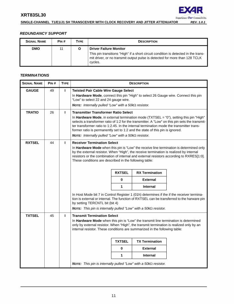
DMO 11 O Driver Failure MonitorThis pin transitions "High" if a short circuit condition is detected in the trans-mit driver, or no transmit output pulse is detected for more than 128 TCLK cycles.
TERMINATIONS
SIGNAL NAME PIN # TYPE DESCRIPTION
GAUGE 49 I Twisted Pair Cable Wire Gauge SelectIn Hardware Mode, connect this pin "High" to select 26 Gauge wire. Connect this pin “Low” to select 22 and 24 gauge wire.NOTE: Internally pulled “Low” with a 50kΩ resistor.
TRATIO 26 I Transmitter Transformer Ratio SelectIn Hardware Mode, in external termination mode (TXTSEL = “0”), setting this pin "High" selects a transformer ratio of 1:2 for the transmitter. A "Low" on this pin sets the transmit-ter transformer ratio to 1:2.45. In the internal termination mode the transmitter trans-former ratio is permanently set to 1:2 and the state of this pin is ignored. NOTE: Internally pulled "Low" with a 50kΩ resistor.
RXTSEL 44 I Receiver Termination SelectIn Hardware Mode when this pin is “Low” the receive line termination is determined only by the external resistor. When “High”, the receive termination is realized by internal resistors or the combination of internal and external resistors according to RXRES[1:0]. These conditions are described in the following table:
In Host Mode bit 7 in Control Register 1 (01h) determines if the if the receiver termina-tion is external or internal. The function of RXTSEL can be transferred to the harware pin by setting TERCNTL bit (bit 4) NOTE: This pin is internally pulled "Low" with a 50kΩ resistor.
TXTSEL 45 I Transmit Termination SelectIn Hardware Mode when this pin is “Low” the transmit line termination is determined only by external resistor. When “High”, the transmit termination is realized only by an internal resistor. These conditions are summarized in the following table:
NOTE: This pin is internally pulled "Low" with a 50kΩ resistor.
RXTSEL RX Termination
0
1
External
Internal
TXTSEL TX Termination
0
1
External
Internal
11
XRT83SL30REV. 1.0.1 SINGLE-CHANNEL T1/E1/J1 SH TRANSCEIVER WITH CLOCK RECOVERY AND JITTER ATTENUATOR
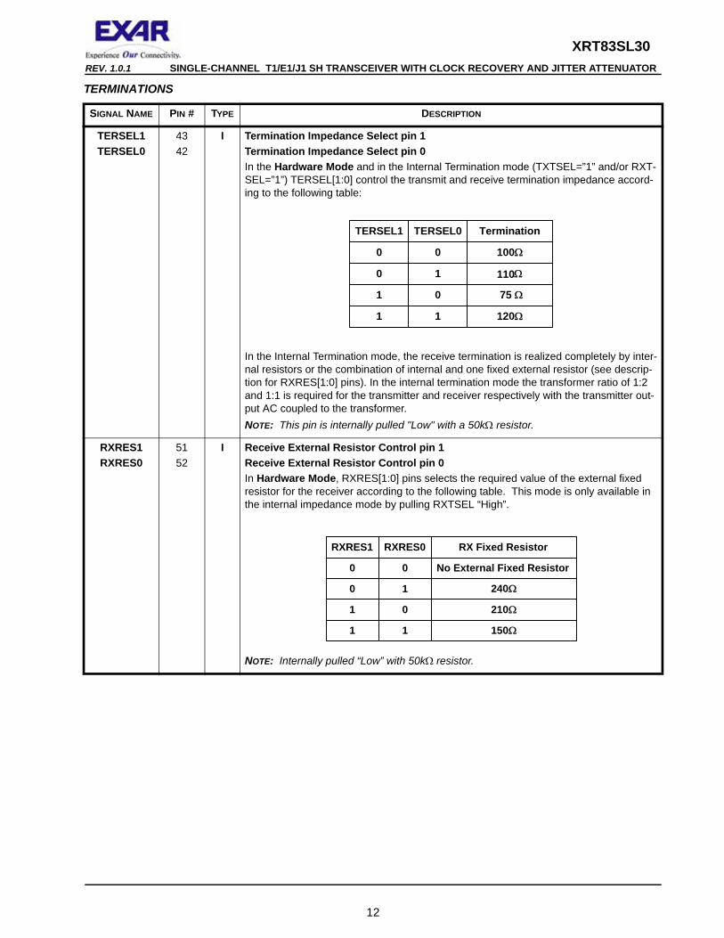
TERSEL1TERSEL0
4342
I Termination Impedance Select pin 1Termination Impedance Select pin 0In the Hardware Mode and in the Internal Termination mode (TXTSEL=”1” and/or RXT-SEL=”1”) TERSEL[1:0] control the transmit and receive termination impedance accord-ing to the following table:
In the Internal Termination mode, the receive termination is realized completely by inter-nal resistors or the combination of internal and one fixed external resistor (see descrip-tion for RXRES[1:0] pins). In the internal termination mode the transformer ratio of 1:2 and 1:1 is required for the transmitter and receiver respectively with the transmitter out-put AC coupled to the transformer.NOTE: This pin is internally pulled "Low" with a 50kΩ resistor.
RXRES1RXRES0
5152
I Receive External Resistor Control pin 1Receive External Resistor Control pin 0In Hardware Mode, RXRES[1:0] pins selects the required value of the external fixed resistor for the receiver according to the following table. This mode is only available in the internal impedance mode by pulling RXTSEL “High”.
NOTE: Internally pulled “Low” with 50kΩ resistor.
TERMINATIONS
SIGNAL NAME PIN # TYPE DESCRIPTION
TERSEL1
0
1
Ω
75 Ω
0
1
0
TerminationTERSEL0
0
11
100Ω
120Ω
110
RXRES1
0
0
RX Fixed Resistor
No External Fixed Resistor
RXRES0
0
1
1
1
210Ω
150Ω
0
1
240Ω
12
XRT83SL30 SINGLE-CHANNEL T1/E1/J1 SH TRANSCEIVER WITH CLOCK RECOVERY AND JITTER ATTENUATOR REV. 1.0.1
CONTROL FUNCTION
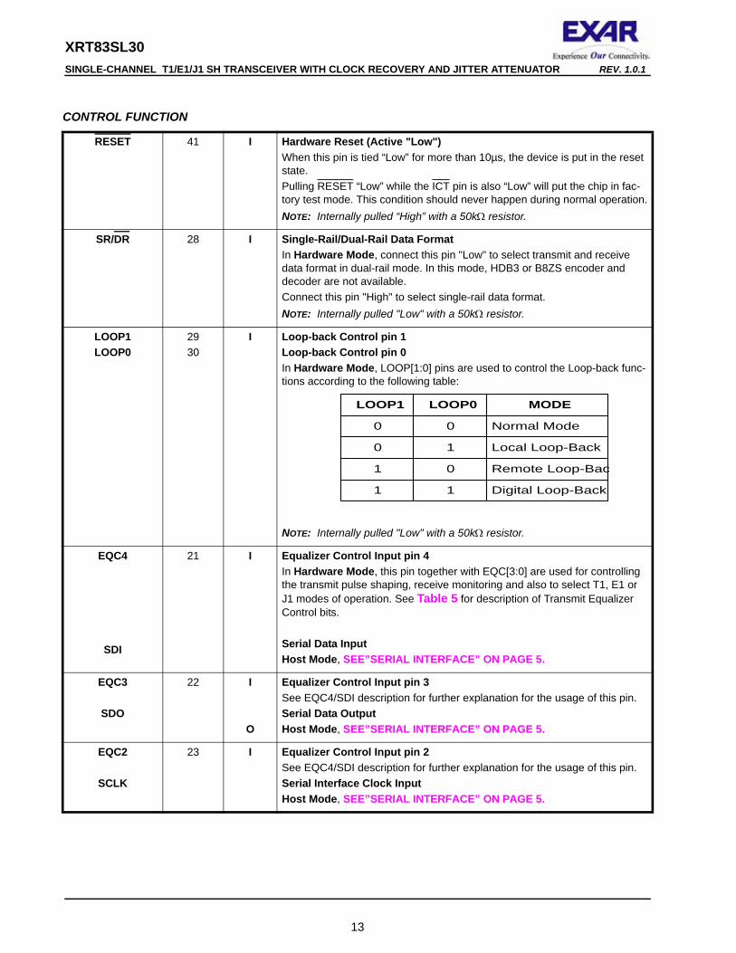
RESET 41 I Hardware Reset (Active "Low")When this pin is tied “Low” for more than 10µs, the device is put in the reset state.Pulling RESET “Low” while the ICT pin is also “Low” will put the chip in fac-tory test mode. This condition should never happen during normal operation.NOTE: Internally pulled “High” with a 50kΩ resistor.
SR/DR 28 I Single-Rail/Dual-Rail Data FormatIn Hardware Mode, connect this pin "Low" to select transmit and receive data format in dual-rail mode. In this mode, HDB3 or B8ZS encoder and decoder are not available.Connect this pin "High" to select single-rail data format.NOTE: Internally pulled "Low" with a 50kΩ resistor.
LOOP1LOOP0
2930
I Loop-back Control pin 1Loop-back Control pin 0In Hardware Mode, LOOP[1:0] pins are used to control the Loop-back func-tions according to the following table:
NOTE: Internally pulled "Low" with a 50kΩ resistor.
EQC4
SDI
21 I Equalizer Control Input pin 4In Hardware Mode, this pin together with EQC[3:0] are used for controlling the transmit pulse shaping, receive monitoring and also to select T1, E1 or J1 modes of operation. See Table 5 for description of Transmit Equalizer Control bits.
Serial Data Input Host Mode, SEE”SERIAL INTERFACE” ON PAGE 5.
EQC3
SDO
22 I
O
Equalizer Control Input pin 3See EQC4/SDI description for further explanation for the usage of this pin.Serial Data Output Host Mode, SEE”SERIAL INTERFACE” ON PAGE 5.
EQC2
SCLK
23 I Equalizer Control Input pin 2See EQC4/SDI description for further explanation for the usage of this pin.Serial Interface Clock InputHost Mode, SEE”SERIAL INTERFACE” ON PAGE 5.
LOOP1 LOOP0
0 0
0 1
1 0
1 1
MODE
Normal Mode
Local Loop-Back
Remote Loop-Bac
Digital Loop-Back
13
XRT83SL30REV. 1.0.1 SINGLE-CHANNEL T1/E1/J1 SH TRANSCEIVER WITH CLOCK RECOVERY AND JITTER ATTENUATOR
EQC1
CS
24 I Equalizer Control Input pin 1See EQC4/SDI description for further explanation for the usage of this pin.Chip Select Input Host Mode, SEE”SERIAL INTERFACE” ON PAGE 5.
EQC0
INT
25 I
O
Equalizer Control Input pin 0See EQC4/SDI description for further explanation for the usage of this pin.Interrupt OutputHost Mode, SEE”SERIAL INTERFACE” ON PAGE 5.
ALARM FUNCTION/OTHER
SIGNAL NAME PIN # TYPE DESCRIPTION
ATAOS 27 I Automatic Transmit “All Ones” PatternIn Hardware Mode, a "High" level on this pin enables the automatic trans-mission of an "All Ones" AMI pattern from the transmitter when the receiver has detected an LOS condition. A "Low" level on this pin disables this func-tion.NOTE: This pin is internally pulled “Low” with a 50kΩ resistor.
ICT 59 I In-Circuit Testing (active "Low")When this pin is tied “Low”, all output pins are forced to a “High” impedance state for in-circuit testing.Pulling RESET “Low” while ICT pin is also “Low” will put the chip in factory test mode. This condition should never happen during normal operation.NOTE: Internally pulled “High” with a 50kΩ resistor.
CONTROL FUNCTION
14
XRT83SL30 SINGLE-CHANNEL T1/E1/J1 SH TRANSCEIVER WITH CLOCK RECOVERY AND JITTER ATTENUATOR REV. 1.0.1
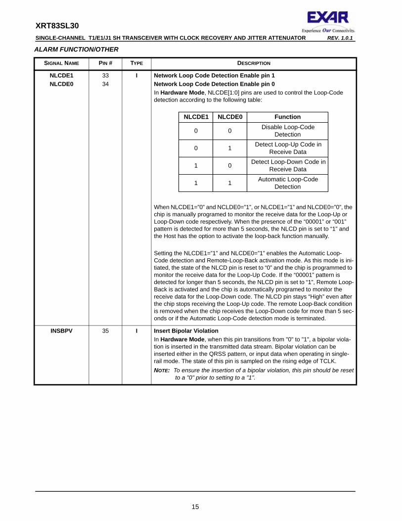
NLCDE1NLCDE0
3334
I Network Loop Code Detection Enable pin 1Network Loop Code Detection Enable pin 0In Hardware Mode, NLCDE[1:0] pins are used to control the Loop-Code detection according to the following table:
When NLCDE1=”0” and NCLDE0=”1”, or NLCDE1=”1” and NLCDE0=”0”, the chip is manually programed to monitor the receive data for the Loop-Up or Loop-Down code respectively. When the presence of the “00001” or “001” pattern is detected for more than 5 seconds, the NLCD pin is set to “1” and the Host has the option to activate the loop-back function manually.
Setting the NLCDE1=”1” and NLCDE0=”1” enables the Automatic Loop-Code detection and Remote-Loop-Back activation mode. As this mode is ini-tiated, the state of the NLCD pin is reset to “0” and the chip is programmed to monitor the receive data for the Loop-Up Code. If the “00001” pattern is detected for longer than 5 seconds, the NLCD pin is set to “1”, Remote Loop-Back is activated and the chip is automatically programed to monitor the receive data for the Loop-Down code. The NLCD pin stays “High” even after the chip stops receiving the Loop-Up code. The remote Loop-Back condition is removed when the chip receives the Loop-Down code for more than 5 sec-onds or if the Automatic Loop-Code detection mode is terminated.
INSBPV 35 I Insert Bipolar ViolationIn Hardware Mode, when this pin transitions from "0" to "1", a bipolar viola-tion is inserted in the transmitted data stream. Bipolar violation can be inserted either in the QRSS pattern, or input data when operating in single-rail mode. The state of this pin is sampled on the rising edge of TCLK. NOTE: To ensure the insertion of a bipolar violation, this pin should be reset
to a "0" prior to setting to a "1".
ALARM FUNCTION/OTHER
SIGNAL NAME PIN # TYPE DESCRIPTION
NLCDE1 NLCDE0 Function
0 0 Disable Loop-CodeDetection
0 1 Detect Loop-Up Code inReceive Data
1 1 Automatic Loop-CodeDetection
1 0 Detect Loop-Down Code inReceive Data
15
XRT83SL30REV. 1.0.1 SINGLE-CHANNEL T1/E1/J1 SH TRANSCEIVER WITH CLOCK RECOVERY AND JITTER ATTENUATOR
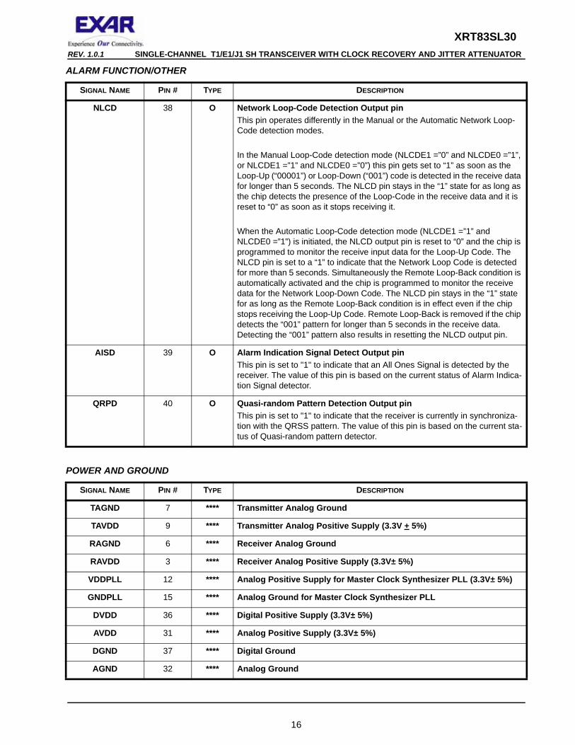
NLCD 38 O Network Loop-Code Detection Output pinThis pin operates differently in the Manual or the Automatic Network Loop-Code detection modes.
In the Manual Loop-Code detection mode (NLCDE1 =”0” and NLCDE0 =”1”, or NLCDE1 =”1” and NLCDE0 =”0”) this pin gets set to “1” as soon as the Loop-Up (“00001”) or Loop-Down (“001”) code is detected in the receive data for longer than 5 seconds. The NLCD pin stays in the “1” state for as long as the chip detects the presence of the Loop-Code in the receive data and it is reset to “0” as soon as it stops receiving it.
When the Automatic Loop-Code detection mode (NLCDE1 =”1” and NLCDE0 =”1”) is initiated, the NLCD output pin is reset to “0” and the chip is programmed to monitor the receive input data for the Loop-Up Code. The NLCD pin is set to a “1” to indicate that the Network Loop Code is detected for more than 5 seconds. Simultaneously the Remote Loop-Back condition is automatically activated and the chip is programmed to monitor the receive data for the Network Loop-Down Code. The NLCD pin stays in the “1” state for as long as the Remote Loop-Back condition is in effect even if the chip stops receiving the Loop-Up Code. Remote Loop-Back is removed if the chip detects the “001” pattern for longer than 5 seconds in the receive data. Detecting the “001” pattern also results in resetting the NLCD output pin.
AISD 39 O Alarm Indication Signal Detect Output pinThis pin is set to "1" to indicate that an All Ones Signal is detected by the receiver. The value of this pin is based on the current status of Alarm Indica-tion Signal detector.
QRPD 40 O Quasi-random Pattern Detection Output pinThis pin is set to "1" to indicate that the receiver is currently in synchroniza-tion with the QRSS pattern. The value of this pin is based on the current sta-tus of Quasi-random pattern detector.
POWER AND GROUND
SIGNAL NAME PIN # TYPE DESCRIPTION
TAGND 7 **** Transmitter Analog Ground
TAVDD 9 **** Transmitter Analog Positive Supply (3.3V + 5%)
RAGND 6 **** Receiver Analog Ground
RAVDD 3 **** Receiver Analog Positive Supply (3.3V± 5%)
VDDPLL 12 **** Analog Positive Supply for Master Clock Synthesizer PLL (3.3V± 5%)
GNDPLL 15 **** Analog Ground for Master Clock Synthesizer PLL
DVDD 36 **** Digital Positive Supply (3.3V± 5%)
AVDD 31 **** Analog Positive Supply (3.3V± 5%)
DGND 37 **** Digital Ground
AGND 32 **** Analog Ground
ALARM FUNCTION/OTHER
SIGNAL NAME PIN # TYPE DESCRIPTION
16
XRT83SL30 SINGLE-CHANNEL T1/E1/J1 SH TRANSCEIVER WITH CLOCK RECOVERY AND JITTER ATTENUATOR REV. 1.0.1
FUNCTIONAL DESCRIPTIONThe XRT83SL30 is a fully integrated single channel short-haul transceiver intended for T1, J1 or E1 systems. Simplified block diagrams of the device are shown in Figure 1, Host mode and Figure 2, Hardware mode.
In T1 applications, the XRT83SL30 can generate five transmit pulse shapes to meet the short-haul Digital Cross-connect (DSX-1) template requirement. It also provides programmable transmit output pulse generator that can be used for output pulse shaping allowing performance improvement over a wide variety of conditions. The operation and configuration of the XRT83SL30 can be controlled through a serial microprocessor Hostinterface or, by Hardware control.
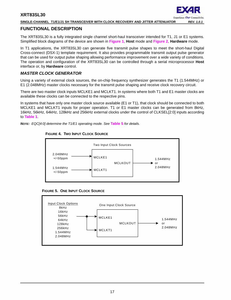
MASTER CLOCK GENERATORUsing a variety of external clock sources, the on-chip frequency synthesizer generates the T1 (1.544MHz) or E1 (2.048MHz) master clocks necessary for the transmit pulse shaping and receive clock recovery circuit.
There are two master clock inputs MCLKE1 and MCLKT1. In systems where both T1 and E1 master clocks are available these clocks can be connected to the respective pins.
In systems that have only one master clock source available (E1 or T1), that clock should be connected to both MCLKE1 and MCLKT1 inputs for proper operation. T1 or E1 master clocks can be generated from 8kHz, 16kHz, 56kHz, 64kHz, 128kHz and 256kHz external clocks under the control of CLKSEL[2:0] inputs according to Table 1.
NOTE: EQC[4:0] determine the T1/E1 operating mode. See Table 5 for details.
FIGURE 4. TWO INPUT CLOCK SOURCE
FIGURE 5. ONE INPUT CLOCK SOURCE
MCLKE1
MCLKT1
MCLKOUT1.544MHzor2.048MHz
2.048MHz+/-50ppm
1.544MHz+/-50ppm
Two Input Clock Sources
MCLKE1
MCLKT1
MCLKOUT1.544MHzor2.048MHz
One Input Clock SourceInput Clock Options8kHz
16kHz56kHz64kHz
128kHz256kHz
1.544MHz2.048MHz
17
XRT83SL30REV. 1.0.1 SINGLE-CHANNEL T1/E1/J1 SH TRANSCEIVER WITH CLOCK RECOVERY AND JITTER ATTENUATOR
In Host mode the programming is achieved through the corresponding interface control bits, the state of the CLKSEL[2:0] control bits and the state of the MCLKRATE interface control bit.
RECEIVER
RECEIVER INPUTAt the receiver input, a cable attenuated AMI signal can be coupled to the receiver through a capacitor or a 1:1 transformer. The input signal is first applied to a selective equalizer for signal conditioning. The maximum equalizer gain is up to 15dB for T1 and E1 modes. The equalized signal is subsequently applied to a peak detector which in turn controls the equalizer settings and the data slicer. The slicer threshold for both E1 and T1 is typically set at 50% of the peak amplitude at the equalizer output. After the slicers, the digital representation of the AMI signals are applied to the clock and data recovery circuit. The recovered data subsequently goes through the jitter attenuator and decoder (if selected) for HDB3 or B8ZS decoding before being applied to the RPOS/RDATA and RNEG/LCV pins. Clock recovery is accomplished by a digital phase-locked loop (DPLL) which does not require any external components and can tolerate high levels of input jitter that meets or exceeds the ITU-G.823 and TR-TSY000499 standards.
In Hardware mode only, this receive channel is turned on upon power-up and is always on. In Host mode, the receiver can be turned on or off with the RXON bit. SEE”MICROPROCESSOR REGISTER #2 BIT DESCRIPTION” ON PAGE 47.
TABLE 1: MASTER CLOCK GENERATOR
MCLKE1KHZ
MCLKT1KHZ
CLKSEL2 CLKSEL1 CLKSEL0 MCLKRATEMASTER CLOCK
KHZ
2048 2048 0 0 0 0 2048
2048 2048 0 0 0 1 1544
2048 1544 0 0 0 0 2048
1544 1544 0 0 1 1 1544
1544 1544 0 0 1 0 2048
2048 1544 0 0 1 1 1544
8 x 0 1 0 0 2048
8 x 0 1 0 1 1544
16 x 0 1 1 0 2048
16 x 0 1 1 1 1544
56 x 1 0 0 0 2048
56 x 1 0 0 1 1544
64 x 1 0 1 0 2048
64 x 1 0 1 1 1544
128 x 1 1 0 0 2048
128 x 1 1 0 1 1544
256 x 1 1 1 0 2048
256 x 1 1 1 1 1544
18
XRT83SL30 SINGLE-CHANNEL T1/E1/J1 SH TRANSCEIVER WITH CLOCK RECOVERY AND JITTER ATTENUATOR REV. 1.0.1
RECEIVE MONITOR MODEIn applications where Monitor mode is desired, the equalizer can be configured in a gain mode which handles input signals attenuated resistively up to 29dB, along with 0 to 6dB cable attenuation for both T1 and E1 applications, refer to Table 5 for details. This feature is available in both Hardware and Host modes.
RECEIVER LOSS OF SIGNAL (RLOS)For compatibility with ITU G.775 requirements, the RLOS monitoring function is implemented using both analog and digital detection schemes. If the analog RLOS condition occurs, a digital detector is activated to count for 32 consecutive zeros in E1 (4096 bits in Extended Los mode, EXLOS = “1”) or 175 consecutive zeros in T1 before RLOS is asserted. RLOS is cleared when the input signal rises +3dB (built in hysteresis) above the point at which it was declared and meets 12.5% ones density of 4 ones in a 32 bit window, with no more than 16 consecutive zeros for E1. In T1 mode, RLOS is cleared when the input signal rises +3dB (built in hysteresis) above the point at which it was declared and contains 16 ones in a 128 bit window with no more than 100 consecutive zeros in the data stream. When loss of signal occurs, RLOS register indication and register status will change. If the RLOS register enable is set high (enabled), the alarm will trigger an interrupt causing the interrupt pin (INT) to go low. Once the alarm status register has been read, it will automatically reset upon read (RUR), and the INT pin will return high.
Analog RLOS
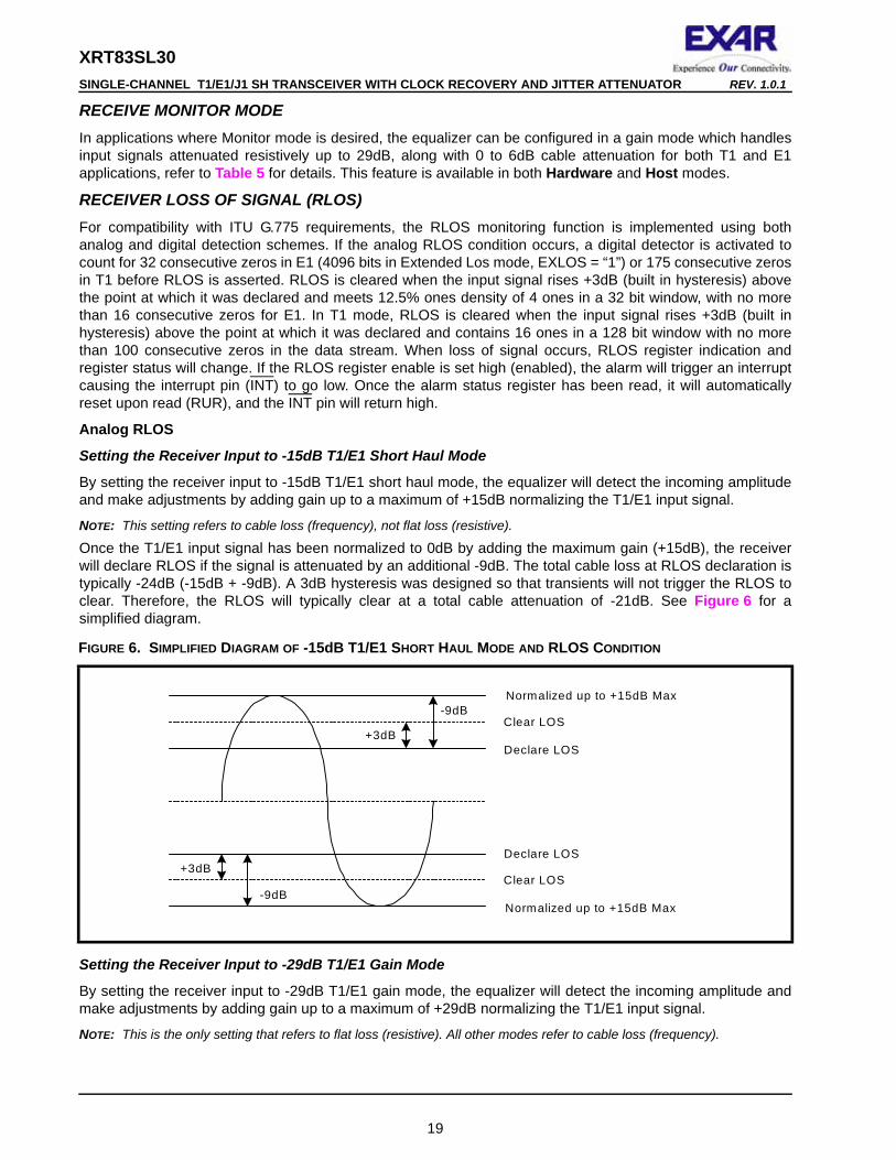
Setting the Receiver Input to -15dB T1/E1 Short Haul Mode
By setting the receiver input to -15dB T1/E1 short haul mode, the equalizer will detect the incoming amplitude and make adjustments by adding gain up to a maximum of +15dB normalizing the T1/E1 input signal.
NOTE: This setting refers to cable loss (frequency), not flat loss (resistive).
Once the T1/E1 input signal has been normalized to 0dB by adding the maximum gain (+15dB), the receiver will declare RLOS if the signal is attenuated by an additional -9dB. The total cable loss at RLOS declaration is typically -24dB (-15dB + -9dB). A 3dB hysteresis was designed so that transients will not trigger the RLOS to clear. Therefore, the RLOS will typically clear at a total cable attenuation of -21dB. See Figure 6 for a simplified diagram.
Setting the Receiver Input to -29dB T1/E1 Gain Mode
By setting the receiver input to -29dB T1/E1 gain mode, the equalizer will detect the incoming amplitude and make adjustments by adding gain up to a maximum of +29dB normalizing the T1/E1 input signal.
NOTE: This is the only setting that refers to flat loss (resistive). All other modes refer to cable loss (frequency).
FIGURE 6. SIMPLIFIED DIAGRAM OF -15dB T1/E1 SHORT HAUL MODE AND RLOS CONDITION
Normalized up to +15dB Max
Normalized up to +15dB Max
Declare LOS
Clear LOS-9dB
+3dB
Clear LOS
Declare LOS+3dB
-9dB
19
XRT83SL30REV. 1.0.1 SINGLE-CHANNEL T1/E1/J1 SH TRANSCEIVER WITH CLOCK RECOVERY AND JITTER ATTENUATOR
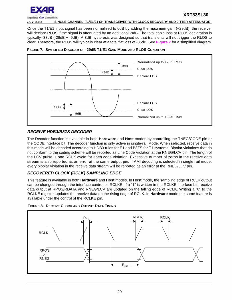
Once the T1/E1 input signal has been normalized to 0dB by adding the maximum gain (+29dB), the receiver will declare RLOS if the signal is attenuated by an additional -9dB. The total cable loss at RLOS declaration is typically -38dB (-29dB + -9dB). A 3dB hysteresis was designed so that transients will not trigger the RLOS to clear. Therefore, the RLOS will typically clear at a total flat loss of -35dB. See Figure 7 for a simplified diagram.
RECEIVE HDB3/B8ZS DECODERThe Decoder function is available in both Hardware and Host modes by controlling the TNEG/CODE pin or the CODE interface bit. The decoder function is only active in single-rail Mode. When selected, receive data in this mode will be decoded according to HDB3 rules for E1 and B8ZS for T1 systems. Bipolar violations that do not conform to the coding scheme will be reported as Line Code Violation at the RNEG/LCV pin. The length of the LCV pulse is one RCLK cycle for each code violation. Excessive number of zeros in the receive data stream is also reported as an error at the same output pin. If AMI decoding is selected in single rail mode, every bipolar violation in the receive data stream will be reported as an error at the RNEG/LCV pin.
RECOVERED CLOCK (RCLK) SAMPLING EDGEThis feature is available in both Hardware and Host modes. In Host mode, the sampling edge of RCLK output can be changed through the interface control bit RCLKE. If a “1” is written in the RCLKE interface bit, receive data output at RPOS/RDATA and RNEG/LCV are updated on the falling edge of RCLK. Writing a “0” to the RCLKE register, updates the receive data on the rising edge of RCLK. In Hardware mode the same feature is available under the control of the RCLKE pin.
FIGURE 7. SIMPLIFIED DIAGRAM OF -29dB T1/E1 GAIN MODE AND RLOS CONDITION
FIGURE 8. RECEIVE CLOCK AND OUTPUT DATA TIMING
Normalized up to +29dB Max
Normalized up to +29dB Max
Declare LOS
Clear LOS-9dB
+3dB
Clear LOS
Declare LOS+3dB
-9dB
RCLKR RCLKF
RCLK
RPOSor
RNEG
RDY
RHO
20
XRT83SL30 SINGLE-CHANNEL T1/E1/J1 SH TRANSCEIVER WITH CLOCK RECOVERY AND JITTER ATTENUATOR REV. 1.0.1
JITTER ATTENUATORTo reduce phase and frequency jitter in the recovered clock, the jitter attenuator can be placed in the receive signal path. The jitter attenuator uses a data FIFO (First In First Out) with a programmable depth that can vary between 2x32 and 2x64. The jitter attenuator can also be placed in the transmit signal path or disabled altogether depending upon system requirements. The jitter attenuator, other than using the master clock as reference, requires no external components. With the jitter attenuator selected, the typical throughput delay from input to output is 16 bits for 32 bit FIFO size or 32 bits for 64 bit FIFO size. When the read and write pointers of the FIFO in the jitter attenuator are within two bits of over-flowing or under-flowing, the bandwidth of the jitter attenuator is widened to track the short term input jitter, thereby avoiding data corruption. When this situation occurs, the jitter attenuator will not attenuate input jitter until the read/write pointer's position is outside the two bits window. Under normal condition, the jitter transfer characteristic meets the narrow bandwidth requirement as specified in ITU- G.736, ITU- I.431 and AT&T Pub 62411 standards.
In T1 mode the Jitter Attenuator Bandwidth is always set to 3Hz. In E1 mode, the bandwidth can be reduced through the JABW control signal. When JABW is set “High” the bandwidth of the jitter attenuator is reduced from 10Hz to 1.5Hz. Under this condition the FIFO length is automatically set to 64 bits and the 32 bits FIFO length will not be available in this mode.
GAPPED CLOCK (JA MUST BE ENABLED IN THE TRANSMIT PATH)The XRT83SL30 LIU is ideal for multiplexer or mapper applications where the network data crosses multiple timing domains. As the higher data rates are de-multiplexed down to T1 or E1 data, stuffing bits are removed which can leave gaps in the incoming data stream. If the jitter attenuator is enabled in the transmit path, the 32-Bit or 64-Bit FIFO is used to smooth the gapped clock into a steady T1 or E1 output. The maximum gap width is shown in Table 2.
NOTE: If the LIU is used in a loop timing system, the jitter attenuator should be enabled in the receive path.
TABLE 2: MAXIMUM GAP WIDTH FOR MULTIPLEXER/MAPPER APPLICATIONS
FIFO DEPTH MAXIMUM GAP WIDTH
32-Bit 20 UI
64-Bit 50 UI
21
XRT83SL30REV. 1.0.1 SINGLE-CHANNEL T1/E1/J1 SH TRANSCEIVER WITH CLOCK RECOVERY AND JITTER ATTENUATOR
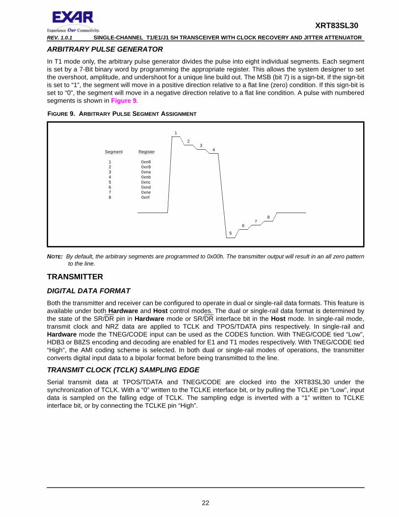
ARBITRARY PULSE GENERATORIn T1 mode only, the arbitrary pulse generator divides the pulse into eight individual segments. Each segment is set by a 7-Bit binary word by programming the appropriate register. This allows the system designer to set the overshoot, amplitude, and undershoot for a unique line build out. The MSB (bit 7) is a sign-bit. If the sign-bit is set to “1”, the segment will move in a positive direction relative to a flat line (zero) condition. If this sign-bit is set to “0”, the segment will move in a negative direction relative to a flat line condition. A pulse with numbered segments is shown in Figure 9.
NOTE: By default, the arbitrary segments are programmed to 0x00h. The transmitter output will result in an all zero pattern to the line.
TRANSMITTER
DIGITAL DATA FORMATBoth the transmitter and receiver can be configured to operate in dual or single-rail data formats. This feature is available under both Hardware and Host control modes. The dual or single-rail data format is determined by the state of the SR/DR pin in Hardware mode or SR/DR interface bit in the Host mode. In single-rail mode, transmit clock and NRZ data are applied to TCLK and TPOS/TDATA pins respectively. In single-rail and Hardware mode the TNEG/CODE input can be used as the CODES function. With TNEG/CODE tied “Low”, HDB3 or B8ZS encoding and decoding are enabled for E1 and T1 modes respectively. With TNEG/CODE tied “High”, the AMI coding scheme is selected. In both dual or single-rail modes of operations, the transmitter converts digital input data to a bipolar format before being transmitted to the line.
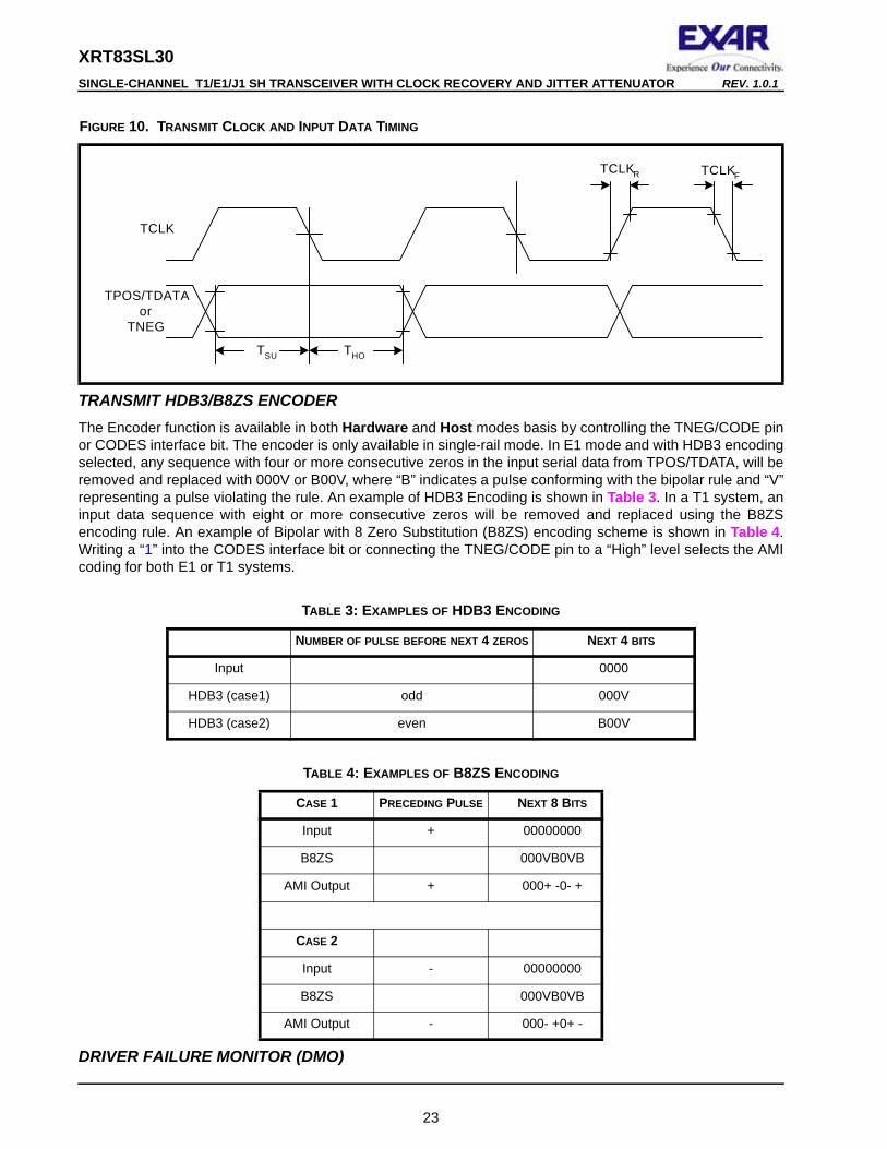
TRANSMIT CLOCK (TCLK) SAMPLING EDGESerial transmit data at TPOS/TDATA and TNEG/CODE are clocked into the XRT83SL30 under the synchronization of TCLK. With a “0” written to the TCLKE interface bit, or by pulling the TCLKE pin “Low”, input data is sampled on the falling edge of TCLK. The sampling edge is inverted with a “1” written to TCLKE interface bit, or by connecting the TCLKE pin “High”.
FIGURE 9. ARBITRARY PULSE SEGMENT ASSIGNMENT
1
23
4
5
67
8
Segment Register
1 0xn8 2 0xn9 3 0xna 4 0xnb 5 0xnc 6 0xnd 7 0xne 8 0xnf
22
XRT83SL30 SINGLE-CHANNEL T1/E1/J1 SH TRANSCEIVER WITH CLOCK RECOVERY AND JITTER ATTENUATOR REV. 1.0.1
TRANSMIT HDB3/B8ZS ENCODERThe Encoder function is available in both Hardware and Host modes basis by controlling the TNEG/CODE pin or CODES interface bit. The encoder is only available in single-rail mode. In E1 mode and with HDB3 encoding selected, any sequence with four or more consecutive zeros in the input serial data from TPOS/TDATA, will be removed and replaced with 000V or B00V, where “B” indicates a pulse conforming with the bipolar rule and “V” representing a pulse violating the rule. An example of HDB3 Encoding is shown in Table 3. In a T1 system, an input data sequence with eight or more consecutive zeros will be removed and replaced using the B8ZS encoding rule. An example of Bipolar with 8 Zero Substitution (B8ZS) encoding scheme is shown in Table 4. Writing a “1” into the CODES interface bit or connecting the TNEG/CODE pin to a “High” level selects the AMI coding for both E1 or T1 systems.
DRIVER FAILURE MONITOR (DMO)
FIGURE 10. TRANSMIT CLOCK AND INPUT DATA TIMING
TABLE 3: EXAMPLES OF HDB3 ENCODING
NUMBER OF PULSE BEFORE NEXT 4 ZEROS NEXT 4 BITS
Input 0000
HDB3 (case1) odd 000V
HDB3 (case2) even B00V
TABLE 4: EXAMPLES OF B8ZS ENCODING
CASE 1 PRECEDING PULSE NEXT 8 BITS
Input + 00000000
B8ZS 000VB0VB
AMI Output + 000+ -0- +
CASE 2
Input - 00000000
B8ZS 000VB0VB
AMI Output - 000- +0+ -
TCLKR TCLKF
TCLK
TPOS/TDATAor
TNEG
TSU THO
23
XRT83SL30REV. 1.0.1 SINGLE-CHANNEL T1/E1/J1 SH TRANSCEIVER WITH CLOCK RECOVERY AND JITTER ATTENUATOR
The driver monitor circuit is used to detect transmit driver failure by monitoring the activities at TTIP and TRING. Driver failure may be caused by a short circuit in the primary transformer or system problems at the transmit input. If the transmitter has no output for more than 128 clock cycles, the corresponding DMO pin goes “High” and remains “High” until a valid transmit pulse is detected. In Host mode, the failure of the transmit channel is reported in the corresponding interface bit. If the DMOIE bit is also enabled, any transition on the DMO interface bit will generate an interrupt. The driver failure monitor is supported in both Hardware and Hostmodes.
TRANSMIT PULSE SHAPER & LINE BUILD OUT (LBO) CIRCUITThe transmit pulse shaper circuit uses the high speed clock from the Master timing generator to control the shape and width of the transmitted pulse. The internal high-speed timing generator eliminates the need for a tightly controlled transmit clock (TCLK) duty cycle. With the jitter attenuator not in the transmit path, the transmit output will generate no more than 0.025Unit Interval (UI) peak-to-peak jitter. In Hardware mode, the state of the EQC[4:0] pins determine the transmit pulse shape. In Host mode transmit pulse shape can be controlled using the interface bits EQC[4:0]. The chip supports five fixed transmit pulse settings for T1 Short-haul applications plus a fully programmable waveform generator for arbitrary transmit output pulse shapes. The choice of the transmit pulse shape under the control of the interface bits are summarized in Table 5.
NOTE: EQC[4:0] determine the T1/E1 operating mode of the XRT83SL30. When EQC4 = “1” and EQC3 = “1”, the XRT83SL30 is in the E1 mode, otherwise it is in the T1/J1 mode.
TABLE 5: RECEIVE EQUALIZER CONTROL AND TRANSMIT LINE BUILD-OUT SETTINGS
EQC4 EQC3 EQC2 EQC1 EQC0 T1/E1 MODE & RECEIVE SENSITIVITY
TRANSMIT LBO CABLE CODING
0 1 0 0 0 T1 Short Haul/15dB 0-133 ft./ 0.6dB 100Ω/ TP B8ZS
0 1 0 0 1 T1 Short Haul/15dB 133-266 ft./ 1.2dB 100Ω/ TP B8ZS
0 1 0 1 0 T1 Short Haul/15dB 266-399 ft./ 1.8dB 100Ω/ TP B8ZS
0 1 0 1 1 T1 Short Haul/15dB 399-533 ft./ 2.4dB 100Ω/ TP B8ZS
0 1 1 0 0 T1 Short Haul/15dB 533-655 ft./ 3.0dB 100Ω/ TP B8ZS
0 1 1 0 1 T1 Short Haul/15dB Arbitrary Pulse 100Ω/ TP B8ZS
0 1 1 1 0 T1 Gain Mode/29dB 0-133 ft./ 0.6dB 100Ω/ TP B8ZS
0 1 1 1 1 T1 Gain Mode/29dB 133-266 ft./ 1.2dB 100Ω/ TP B8ZS
1 0 0 0 0 T1 Gain Mode/29dB 266-399 ft./ 1.8dB 100Ω/ TP B8ZS
1 0 0 0 1 T1 Gain Mode/29dB 399-533 ft./ 2.4dB 100Ω/ TP B8ZS
1 0 0 1 0 T1 Gain Mode/29dB 533-655 ft./ 3.0dB 100Ω/ TP B8ZS
1 0 0 1 1 T1 Gain Mode/29dB Arbitrary Pulse 100Ω/ TP B8ZS
1 1 1 0 0 E1 Short Haul ITU G.703 75Ω Coax HDB3
1 1 1 0 1 E1 Short Haul ITU G.703 120Ω TP HDB3
1 1 1 1 0 E1 Gain Mode ITU G.703 75Ω Coax HDB3
1 1 1 1 1 E1 Gain Mode ITU G.703 120Ω TP HDB3
24
XRT83SL30 SINGLE-CHANNEL T1/E1/J1 SH TRANSCEIVER WITH CLOCK RECOVERY AND JITTER ATTENUATOR REV. 1.0.1
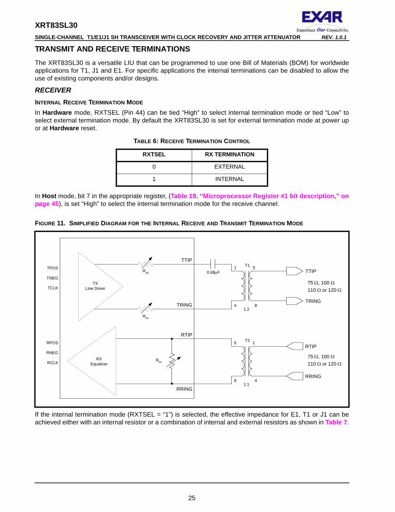
TRANSMIT AND RECEIVE TERMINATIONSThe XRT83SL30 is a versatile LIU that can be programmed to use one Bill of Materials (BOM) for worldwide applications for T1, J1 and E1. For specific applications the internal terminations can be disabled to allow the use of existing components and/or designs.
RECEIVERINTERNAL RECEIVE TERMINATION MODE
In Hardware mode, RXTSEL (Pin 44) can be tied “High” to select internal termination mode or tied “Low” to select external termination mode. By default the XRT83SL30 is set for external termination mode at power up or at Hardware reset.
In Host mode, bit 7 in the appropriate register, (Table 19, “Microprocessor Register #1 bit description,” on page 45), is set “High” to select the internal termination mode for the receive channel.
If the internal termination mode (RXTSEL = “1”) is selected, the effective impedance for E1, T1 or J1 can be achieved either with an internal resistor or a combination of internal and external resistors as shown in Table 7.
TABLE 6: RECEIVE TERMINATION CONTROL
RXTSEL RX TERMINATION
0 EXTERNAL
1 INTERNAL
FIGURE 11. SIMPLIFIED DIAGRAM FOR THE INTERNAL RECEIVE AND TRANSMIT TERMINATION MODE
T1TTIP
TRING
5
81:2
75 Ω, 100 Ω 110 Ω or 120 Ω
4
10.68µF
Rint
Rint
TTIP
TRING
TXLine Driver
T2RTIP
RRING
1
41:1
8
5
RTIP
RRING
RXEqualizer
Rint
TPOS
TNEG
TCLK
RPOS
RNEG
RCLK 75 Ω, 100 Ω 110 Ω or 120 Ω
25
XRT83SL30REV. 1.0.1 SINGLE-CHANNEL T1/E1/J1 SH TRANSCEIVER WITH CLOCK RECOVERY AND JITTER ATTENUATOR
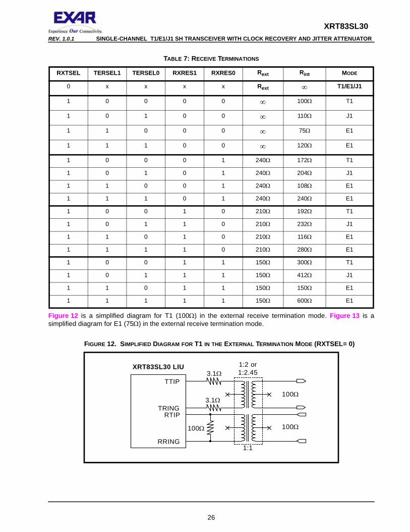
Figure 12 is a simplified diagram for T1 (100Ω) in the external receive termination mode. Figure 13 is a simplified diagram for E1 (75Ω) in the external receive termination mode.
TABLE 7: RECEIVE TERMINATIONS
RXTSEL TERSEL1 TERSEL0 RXRES1 RXRES0 Rext Rint MODE
0 x x x x Rext ∞ T1/E1/J1
1 0 0 0 0 ∞ 100Ω T1
1 0 1 0 0 ∞ 110Ω J1
1 1 0 0 0 ∞ 75Ω E1
1 1 1 0 0 ∞ 120Ω E1
1 0 0 0 1 240Ω 172Ω T1
1 0 1 0 1 240Ω 204Ω J1
1 1 0 0 1 240Ω 108Ω E1
1 1 1 0 1 240Ω 240Ω E1
1 0 0 1 0 210Ω 192Ω T1
1 0 1 1 0 210Ω 232Ω J1
1 1 0 1 0 210Ω 116Ω E1
1 1 1 1 0 210Ω 280Ω E1
1 0 0 1 1 150Ω 300Ω T1
1 0 1 1 1 150Ω 412Ω J1
1 1 0 1 1 150Ω 150Ω E1
1 1 1 1 1 150Ω 600Ω E1
FIGURE 12. SIMPLIFIED DIAGRAM FOR T1 IN THE EXTERNAL TERMINATION MODE (RXTSEL= 0)
3.1Ω
3.1Ω
TTIP
TRINGRTIP
RRING
XRT83SL30 LIU
100Ω
100Ω
100Ω
1:2 or1:2.45
1:1
26
XRT83SL30 SINGLE-CHANNEL T1/E1/J1 SH TRANSCEIVER WITH CLOCK RECOVERY AND JITTER ATTENUATOR REV. 1.0.1
TRANSMITTERTRANSMIT TERMINATION MODE
In Hardware mode, TXTSEL (Pin 45) can be tied “High” to select internal termination mode or tied “Low” for external termination. In Host mode, bit 6 in the appropriate register is set “High” to select the internal termination mode for the transmit channel, see Table 19, “Microprocessor Register #1 bit description,” on page 45.
For internal termination, the transformer turns ratio is always 1:2. In internal mode, no external resistors are used. An external capacitor of 0.68µF is used for proper operation of the internal termination circuitry, see Figure 11.
EXTERNAL TRANSMIT TERMINATION MODE
By default the XRT83SL30 is set for external termination mode at power up or at Hardware reset.
When external transmit termination mode is selected, the internal termination circuitry is disabled. The value of the external resistors is chosen for a specific application according to the turns ratio selected by TRATIO (Pin 26) in Hardware mode or bit 0 in the appropriate register in Host mode, see Table 10 and Table 21, “Microprocessor Register #3 bit description,” on page 49. Figure 12 is a simplified block diagram for T1 (100Ω) in the external termination mode. Figure 13 is a simplified block diagram for E1 (75Ω) in the external termination mode.
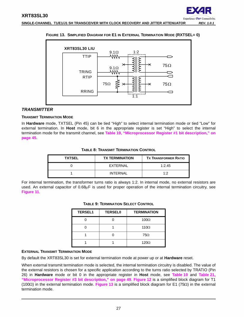
FIGURE 13. SIMPLIFIED DIAGRAM FOR E1 IN EXTERNAL TERMINATION MODE (RXTSEL= 0)
TABLE 8: TRANSMIT TERMINATION CONTROL
TXTSEL TX TERMINATION TX TRANSFORMER RATIO
0 EXTERNAL 1:2.45
1 INTERNAL 1:2
TABLE 9: TERMINATION SELECT CONTROL
TERSEL1 TERSEL0 TERMINATION
0 0 100Ω
0 1 110Ω
1 0 75Ω
1 1 120Ω
9.1 Ω
9.1 Ω
TTIP
TRINGRTIP
RRING
75Ω
XRT83SL30 LIU
75Ω
75Ω
1:2
1:1
27
XRT83SL30REV. 1.0.1 SINGLE-CHANNEL T1/E1/J1 SH TRANSCEIVER WITH CLOCK RECOVERY AND JITTER ATTENUATOR
Table 11 summarizes the transmit terminations.
REDUNDANCY APPLICATIONSTelecommunication system design requires signal integrity and reliability. When a T1/E1 primary line card has a failure, it must be swapped with a backup line card while maintaining connectivity to a backplane without losing data. System designers can achieve this by implementing common redundancy schemes with the XRT83SL30 Line Interface Unit (LIU). The XRT83SL30 offers features that are tailored to redundancy applications while reducing the number of components and providing system designers with solid reference designs. These features allow system designers to implement redundancy applications that ensure reliability. The Internal Impedance mode eliminates the need for external relays when using the 1:1 and 1+1 redundancy schemes.
TABLE 10: TRANSMIT TERMINATION CONTROL
TRATIO TURNS RATIO
0 1:2
1 1:2.45
TABLE 11: TRANSMIT TERMINATIONS
TERSEL1 TERSEL0 TXTSEL TRATIO Rint Ω n Rext Ω Cext
0=EXTERNAL SET BY CONTROL
BITS
n, Rext, AND Cext ARE SUGGESTED SETTINGS1=INTERNAL
T1100 Ω
0 0 0 0 0Ω 2.45 3.1Ω 0
0 0 0 1 0Ω 2 3.1Ω 0
0 0 1 x 100Ω 2 0Ω 0.68µF
J1110 Ω
0 1 0 0 0Ω 2.45 3.1Ω 0
0 1 0 1 0Ω 2 3.1Ω 0
0 1 1 x 110Ω 2 0Ω 0.68µF
E1 75 Ω
1 0 0 0 0Ω 2.45 6.2Ω 0
1 0 0 1 0Ω 2 9.1Ω 0
1 0 1 x 75Ω 2 0Ω 0.68µF
E1120 Ω
1 1 0 0 0Ω 2.45 6.2Ω 0
1 1 0 1 0Ω 2 9.1Ω 0
1 1 1 x 120Ω 2 0Ω 0.68µF
28
XRT83SL30 SINGLE-CHANNEL T1/E1/J1 SH TRANSCEIVER WITH CLOCK RECOVERY AND JITTER ATTENUATOR REV. 1.0.1
PROGRAMMING CONSIDERATIONS
In many applications switching the control of the transmitter outputs and the receiver line impedance to hardware control will provide faster transmitter ON/OFF switching.
In Host Mode, there are two bits in register 18 (12H) that control the transmitter outputs and the Rx line impedance select, TXONCNTL (Bit 5) and TERCNTL (Bit 4).
Setting bit-5 (TXONCNTL) to a “1” transfers the control of the Transmit On/Off function to the TXON Hardwarecontrol pin (pin 58).
Setting bit-4 (TERCNTL) to a “1” transfers the control of the Rx line impedance select (RXTSEL) to the RXTSEL Hardware control pin (pin 44).
Either mode works well with redundancy applications. The user can determine which mode has the fastest switching time for a unique application.
TYPICAL REDUNDANCY SCHEMES
• 1:1 One backup card for every primary card (Facility Protection)
• 1+1 One backup card for every primary card (Line Protection)
• N+1One backup card for N primary cards
1:1 REDUNDANCY
A 1:1 facility protection redundancy scheme has one backup card for every primary card. When using 1:1 redundancy, the backup card has its transmitters tri-stated and its receivers in high impedance. This eliminates the need for external relays and provides one bill of materials for all interface modes of operation. The transmit and receive sections of the LIU device are described separately.
1+1 REDUNDANCY
A 1+1 line protection redundancy scheme has one backup card for every primary card, and the receivers on the backup card are monitoring the receiver inputs. Therefore, the receivers on both cards need to be active. The transmit outputs require no external resistors. The transmit and receive sections of the LIU device are described separately.
TRANSMIT 1:1 & 1+1 REDUNDANCY
For 1:1 and 1+1 redundancy, the transmitters on the primary and backup card should be programmed for Internal Impedance mode. The transmitters on the backup card should be tri-stated. Select the appropriate impedance for the desired mode of operation, T1/E1/J1. A 0.68uF capacitor is used in series with TTIP for blocking DC bias. See Figure 14 for a simplified block diagram of the transmit section for 1:1 and 1+1 redundancy scheme.
NOTE: For simplification, the over voltage protection circuitry was omitted.
29
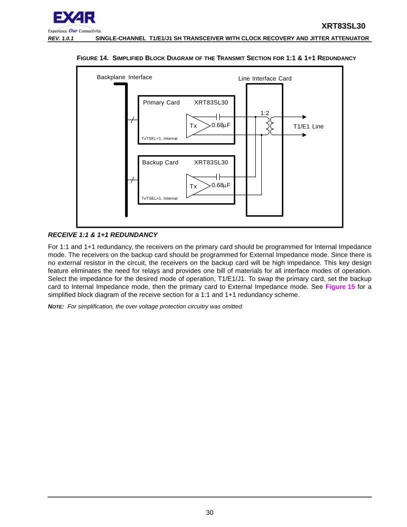
XRT83SL30REV. 1.0.1 SINGLE-CHANNEL T1/E1/J1 SH TRANSCEIVER WITH CLOCK RECOVERY AND JITTER ATTENUATOR
RECEIVE 1:1 & 1+1 REDUNDANCY
For 1:1 and 1+1 redundancy, the receivers on the primary card should be programmed for Internal Impedance mode. The receivers on the backup card should be programmed for External Impedance mode. Since there is no external resistor in the circuit, the receivers on the backup card will be high impedance. This key design feature eliminates the need for relays and provides one bill of materials for all interface modes of operation. Select the impedance for the desired mode of operation, T1/E1/J1. To swap the primary card, set the backup card to Internal Impedance mode, then the primary card to External Impedance mode. See Figure 15 for a simplified block diagram of the receive section for a 1:1 and 1+1 redundancy scheme.
NOTE: For simplification, the over voltage protection circuitry was omitted.
FIGURE 14. SIMPLIFIED BLOCK DIAGRAM OF THE TRANSMIT SECTION FOR 1:1 & 1+1 REDUNDANCY
T1/E1 Line
Backplane Interface
Primary Card
Backup Card XRT83SL30
XRT83SL30
Tx
Tx
Line Interface Card
0.68µF
0.68µF
TxTSEL=1, Internal
TxTSEL=1, Internal
1:2
30
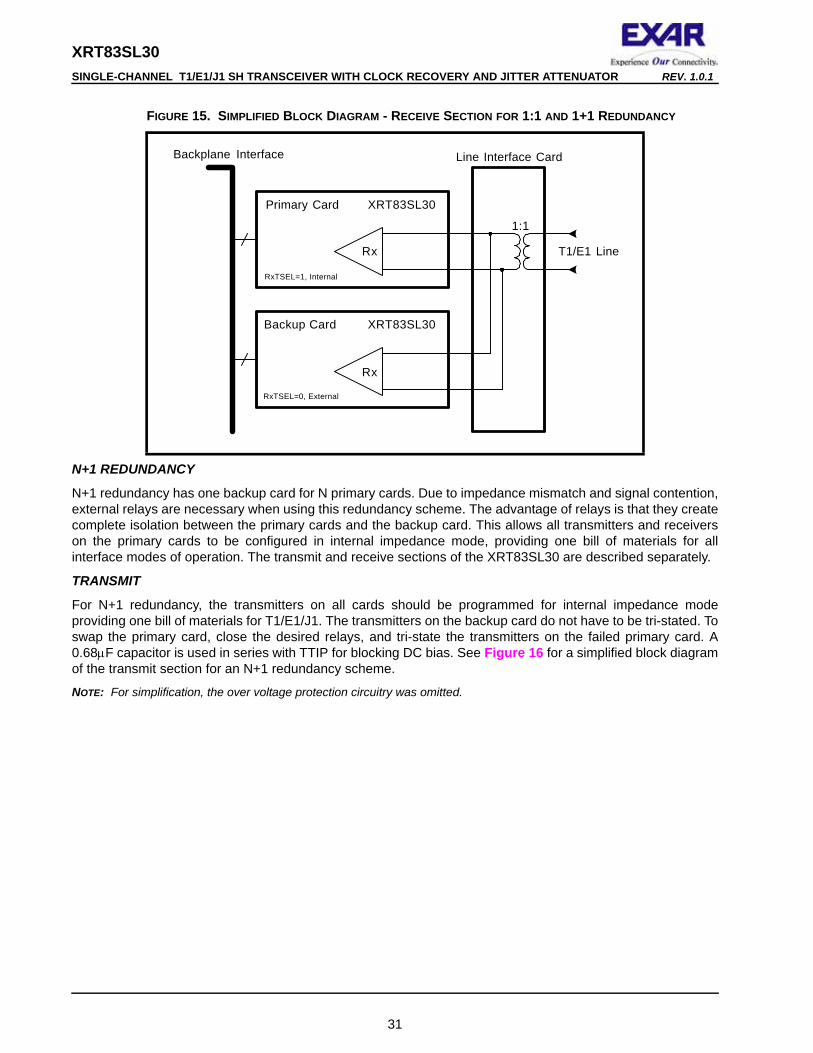
XRT83SL30 SINGLE-CHANNEL T1/E1/J1 SH TRANSCEIVER WITH CLOCK RECOVERY AND JITTER ATTENUATOR REV. 1.0.1
N+1 REDUNDANCY
N+1 redundancy has one backup card for N primary cards. Due to impedance mismatch and signal contention, external relays are necessary when using this redundancy scheme. The advantage of relays is that they create complete isolation between the primary cards and the backup card. This allows all transmitters and receivers on the primary cards to be configured in internal impedance mode, providing one bill of materials for all interface modes of operation. The transmit and receive sections of the XRT83SL30 are described separately.
TRANSMIT
For N+1 redundancy, the transmitters on all cards should be programmed for internal impedance mode providing one bill of materials for T1/E1/J1. The transmitters on the backup card do not have to be tri-stated. To swap the primary card, close the desired relays, and tri-state the transmitters on the failed primary card. A 0.68µF capacitor is used in series with TTIP for blocking DC bias. See Figure 16 for a simplified block diagram of the transmit section for an N+1 redundancy scheme.
NOTE: For simplification, the over voltage protection circuitry was omitted.
FIGURE 15. SIMPLIFIED BLOCK DIAGRAM - RECEIVE SECTION FOR 1:1 AND 1+1 REDUNDANCY
RxTSEL=0, External
RxTSEL=1, Internal
Backplane Interface
Primary Card
Backup Card XRT83SL30
XRT83SL30
Rx
Line Interface Card
T1/E1 LineRx
1:1
31
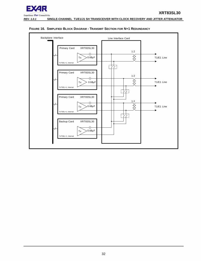
XRT83SL30REV. 1.0.1 SINGLE-CHANNEL T1/E1/J1 SH TRANSCEIVER WITH CLOCK RECOVERY AND JITTER ATTENUATOR
FIGURE 16. SIMPLIFIED BLOCK DIAGRAM - TRANSMIT SECTION FOR N+1 REDUNDANCY
Backplane Interface
Primary Card XRT83SL30
Tx
Line Interface Card
0.68µF T1/E1 Line
Primary Card XRT83SL30
Tx
Primary Card XRT83SL30
Tx
Backup Card XRT83SL30
Tx
T1/E1 Line
T1/E1 Line
TxTSEL=1, Internal
TxTSEL=1, Internal
TxTSEL=1, Internal
TxTSEL=1, Internal
1:2
0.68µF
0.68µF
0.68µF
1:2
1:2
32
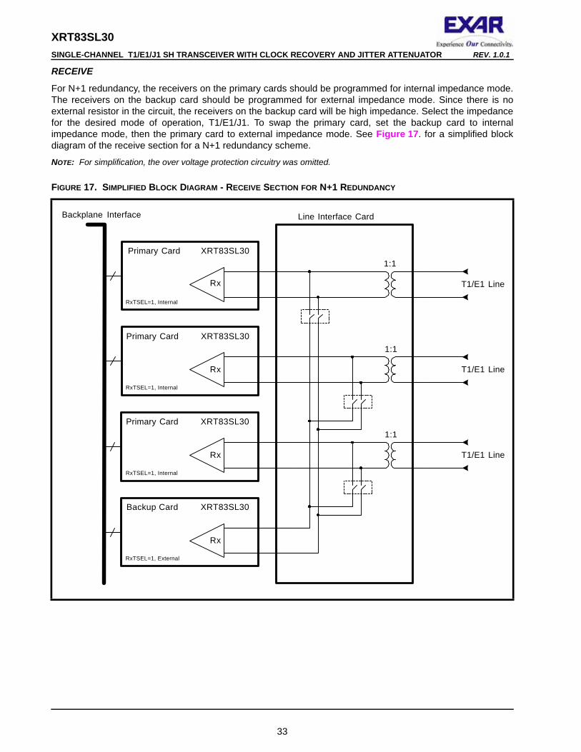
XRT83SL30 SINGLE-CHANNEL T1/E1/J1 SH TRANSCEIVER WITH CLOCK RECOVERY AND JITTER ATTENUATOR REV. 1.0.1
RECEIVE
For N+1 redundancy, the receivers on the primary cards should be programmed for internal impedance mode. The receivers on the backup card should be programmed for external impedance mode. Since there is no external resistor in the circuit, the receivers on the backup card will be high impedance. Select the impedance for the desired mode of operation, T1/E1/J1. To swap the primary card, set the backup card to internal impedance mode, then the primary card to external impedance mode. See Figure 17. for a simplified block diagram of the receive section for a N+1 redundancy scheme.
NOTE: For simplification, the over voltage protection circuitry was omitted.
FIGURE 17. SIMPLIFIED BLOCK DIAGRAM - RECEIVE SECTION FOR N+1 REDUNDANCY
Backplane Interface
Primary Card XRT83SL30
Rx
Line Interface Card
Primary Card XRT83SL30
Rx
Primary Card XRT83SL30
Rx
Backup Card XRT83SL30
Rx
RxTSEL=1, Internal
RxTSEL=1, Internal
RxTSEL=1, Internal
RxTSEL=1, External
T1/E1 Line
T1/E1 Line
T1/E1 Line
1:1
1:1
1:1
33
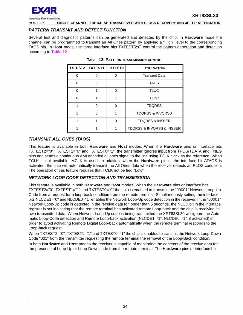
XRT83SL30REV. 1.0.1 SINGLE-CHANNEL T1/E1/J1 SH TRANSCEIVER WITH CLOCK RECOVERY AND JITTER ATTENUATOR
PATTERN TRANSMIT AND DETECT FUNCTIONSeveral test and diagnostic patterns can be generated and detected by the chip. In Hardware mode the channel can be programmed to transmit an All Ones pattern by applying a “High” level to the corresponding TAOS pin. In Host mode, the three interface bits TXTEST[2:0] control the pattern generation and detection according to Table 12.
TRANSMIT ALL ONES (TAOS)This feature is available in both Hardware and Host modes. When the Hardware pins or interface bits TXTEST2="0", TXTEST1="0" and TXTEST0="1", the transmitter ignores input from TPOS/TDATA and TNEG pins and sends a continuous AMI encoded all ones signal to the line using TCLK clock as the reference. When TCLK is not available, MCLK is used. In addition, when the Hardware pin or the interface bit ATAOS is activated, the chip will automatically transmit the All Ones data when the receiver detects an RLOS condition. The operation of this feature requires that TCLK not be tied "Low".
NETWORK LOOP CODE DETECTION AND TRANSMISSIONThis feature is available in both Hardware and Host modes. When the Hardware pins or interface bits TXTEST2="0", TXTEST1="1" and TXTEST0="0" the chip is enabled to transmit the "00001" Network Loop-Up Code from a request for a loop-back condition from the remote terminal. Simultaneously setting the interface bits NLCDE1="0" and NLCDE0="1" enables the Network Loop-Up code detection in the receiver. If the "00001" Network Loop-Up code is detected in the receive data for longer than 5 seconds, the NLCD bit in the interface register is set indicating that the remote terminal has activated remote Loop-back and the chip is receiving its own transmitted data. When Network Loop-Up code is being transmitted the XRT83SL30 will ignore the Auto-matic Loop-Code detection and Remote Loop-back activation (NLCDE1=”1”, NLCDE0=”1”, if activated) in order to avoid activating Remote Digital Loop-back automatically when the remote terminal responds to the Loop-back request.When TXTEST2="0", TXTEST1="1" and TXTEST0="1" the chip is enabled to transmit the Network Loop-Down Code "001" from the transmitter requesting the remote terminal the removal of the Loop-Back condition. In both Hardware and Host modes the receiver is capable of monitoring the contents of the receive data for the presence of Loop-Up or Loop-Down code from the remote terminal. The Hardware pins or interface bits
TABLE 12: PATTERN TRANSMISSION CONTROL
TXTEST2 TXTEST1 TXTEST0 TEST PATTERN
0 0 0 Transmit Data
0 0 1 TAOS
0 1 0 TLUC
0 1 1 TLDC
1 0 0 TDQRSS
1 0 1 TDQRSS & INVQRSS
1 1 0 TDQRSS & INSBER
1 1 1 TDQRSS & INVQRSS & INSBER
34
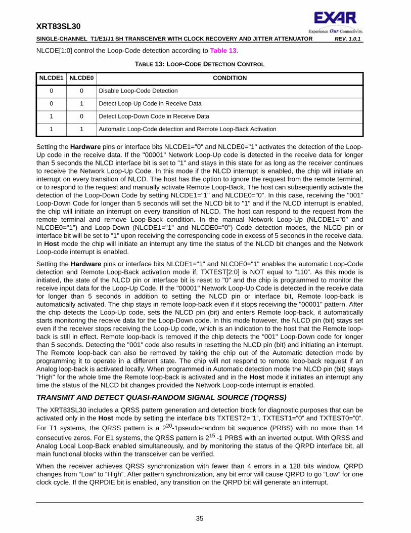
XRT83SL30 SINGLE-CHANNEL T1/E1/J1 SH TRANSCEIVER WITH CLOCK RECOVERY AND JITTER ATTENUATOR REV. 1.0.1
NLCDE[1:0] control the Loop-Code detection according to Table 13.
Setting the Hardware pins or interface bits NLCDE1="0" and NLCDE0="1" activates the detection of the Loop-Up code in the receive data. If the "00001" Network Loop-Up code is detected in the receive data for longer than 5 seconds the NLCD interface bit is set to "1" and stays in this state for as long as the receiver continues to receive the Network Loop-Up Code. In this mode if the NLCD interrupt is enabled, the chip will initiate an interrupt on every transition of NLCD. The host has the option to ignore the request from the remote terminal, or to respond to the request and manually activate Remote Loop-Back. The host can subsequently activate the detection of the Loop-Down Code by setting NLCDE1="1" and NLCDE0="0". In this case, receiving the "001" Loop-Down Code for longer than 5 seconds will set the NLCD bit to "1" and if the NLCD interrupt is enabled, the chip will initiate an interrupt on every transition of NLCD. The host can respond to the request from the remote terminal and remove Loop-Back condition. In the manual Network Loop-Up (NLCDE1="0" and NLCDE0="1") and Loop-Down (NLCDE1="1" and NLCDE0="0") Code detection modes, the NLCD pin or interface bit will be set to "1" upon receiving the corresponding code in excess of 5 seconds in the receive data. In Host mode the chip will initiate an interrupt any time the status of the NLCD bit changes and the Network Loop-code interrupt is enabled.
Setting the Hardware pins or interface bits NLCDE1="1" and NLCDE0="1" enables the automatic Loop-Code detection and Remote Loop-Back activation mode if, TXTEST[2:0] is NOT equal to “110”. As this mode is initiated, the state of the NLCD pin or interface bit is reset to "0" and the chip is programmed to monitor the receive input data for the Loop-Up Code. If the "00001" Network Loop-Up Code is detected in the receive data for longer than 5 seconds in addition to setting the NLCD pin or interface bit, Remote loop-back is automatically activated. The chip stays in remote loop-back even if it stops receiving the "00001" pattern. After the chip detects the Loop-Up code, sets the NLCD pin (bit) and enters Remote loop-back, it automatically starts monitoring the receive data for the Loop-Down code. In this mode however, the NLCD pin (bit) stays set even if the receiver stops receiving the Loop-Up code, which is an indication to the host that the Remote loop-back is still in effect. Remote loop-back is removed if the chip detects the "001" Loop-Down code for longer than 5 seconds. Detecting the "001" code also results in resetting the NLCD pin (bit) and initiating an interrupt. The Remote loop-back can also be removed by taking the chip out of the Automatic detection mode by programming it to operate in a different state. The chip will not respond to remote loop-back request if an Analog loop-back is activated locally. When programmed in Automatic detection mode the NLCD pin (bit) stays "High" for the whole time the Remote loop-back is activated and in the Host mode it initiates an interrupt any time the status of the NLCD bit changes provided the Network Loop-code interrupt is enabled.
TRANSMIT AND DETECT QUASI-RANDOM SIGNAL SOURCE (TDQRSS)The XRT83SL30 includes a QRSS pattern generation and detection block for diagnostic purposes that can be activated only in the Host mode by setting the interface bits TXTEST2=”1”, TXTEST1=”0” and TXTEST0=”0”. For T1 systems, the QRSS pattern is a 220-1pseudo-random bit sequence (PRBS) with no more than 14 consecutive zeros. For E1 systems, the QRSS pattern is 215 -1 PRBS with an inverted output. With QRSS and Analog Local Loop-Back enabled simultaneously, and by monitoring the status of the QRPD interface bit, all main functional blocks within the transceiver can be verified.
When the receiver achieves QRSS synchronization with fewer than 4 errors in a 128 bits window, QRPD changes from “Low” to “High”. After pattern synchronization, any bit error will cause QRPD to go “Low” for one clock cycle. If the QRPDIE bit is enabled, any transition on the QRPD bit will generate an interrupt.
TABLE 13: LOOP-CODE DETECTION CONTROL
NLCDE1 NLCDE0 CONDITION
0 0 Disable Loop-Code Detection
0 1 Detect Loop-Up Code in Receive Data
1 0 Detect Loop-Down Code in Receive Data
1 1 Automatic Loop-Code detection and Remote Loop-Back Activation
35

XRT83SL30REV. 1.0.1 SINGLE-CHANNEL T1/E1/J1 SH TRANSCEIVER WITH CLOCK RECOVERY AND JITTER ATTENUATOR
With TDQRSS activated, a bit error can be inserted in the transmitted QRSS pattern by transitioning the INSBER interface bit from “0” to “1”. Bipolar violation can also be inserted either in the QRSS pattern, or input data when operating in the single-rail mode by transitioning the INSBPV interface bit from “0” to “1”. The state of INSBER and INSBPV bits are sampled on the rising edge of the TCLK. To insure the insertion of the bit error or bipolar violation, a “0” should be written in these bit locations before writing a “1”.
36
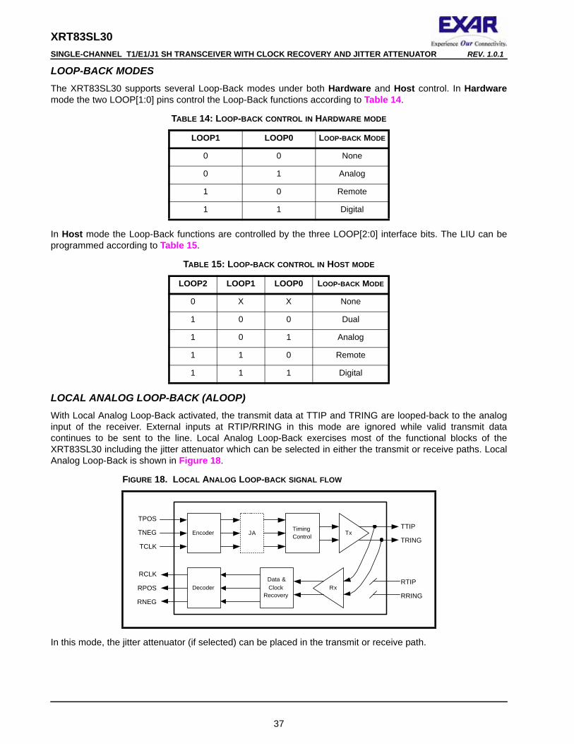
XRT83SL30 SINGLE-CHANNEL T1/E1/J1 SH TRANSCEIVER WITH CLOCK RECOVERY AND JITTER ATTENUATOR REV. 1.0.1
LOOP-BACK MODESThe XRT83SL30 supports several Loop-Back modes under both Hardware and Host control. In Hardwaremode the two LOOP[1:0] pins control the Loop-Back functions according to Table 14.
In Host mode the Loop-Back functions are controlled by the three LOOP[2:0] interface bits. The LIU can be programmed according to Table 15.
LOCAL ANALOG LOOP-BACK (ALOOP)With Local Analog Loop-Back activated, the transmit data at TTIP and TRING are looped-back to the analog input of the receiver. External inputs at RTIP/RRING in this mode are ignored while valid transmit data continues to be sent to the line. Local Analog Loop-Back exercises most of the functional blocks of the XRT83SL30 including the jitter attenuator which can be selected in either the transmit or receive paths. Local Analog Loop-Back is shown in Figure 18.
In this mode, the jitter attenuator (if selected) can be placed in the transmit or receive path.
TABLE 14: LOOP-BACK CONTROL IN HARDWARE MODE
LOOP1 LOOP0 LOOP-BACK MODE
0 0 None
0 1 Analog
1 0 Remote
1 1 Digital
TABLE 15: LOOP-BACK CONTROL IN HOST MODE
LOOP2 LOOP1 LOOP0 LOOP-BACK MODE
0 X X None
1 0 0 Dual
1 0 1 Analog
1 1 0 Remote
1 1 1 Digital
FIGURE 18. LOCAL ANALOG LOOP-BACK SIGNAL FLOW
RxData &Clock
RecoveryDecoder
TPOS
TNEG
TCLK
RCLK
RPOS
RNEG
TxEncoderTimingControlJA
TTIP
TRING
RTIP
RRING
37
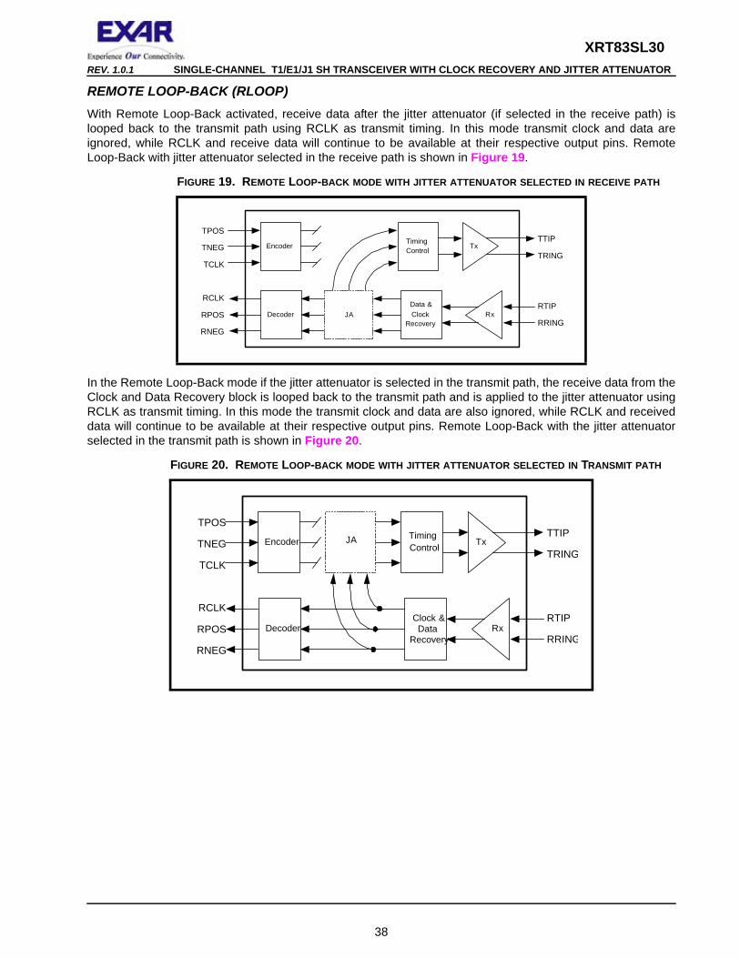
XRT83SL30REV. 1.0.1 SINGLE-CHANNEL T1/E1/J1 SH TRANSCEIVER WITH CLOCK RECOVERY AND JITTER ATTENUATOR
REMOTE LOOP-BACK (RLOOP)With Remote Loop-Back activated, receive data after the jitter attenuator (if selected in the receive path) is looped back to the transmit path using RCLK as transmit timing. In this mode transmit clock and data are ignored, while RCLK and receive data will continue to be available at their respective output pins. Remote Loop-Back with jitter attenuator selected in the receive path is shown in Figure 19.
In the Remote Loop-Back mode if the jitter attenuator is selected in the transmit path, the receive data from the Clock and Data Recovery block is looped back to the transmit path and is applied to the jitter attenuator using RCLK as transmit timing. In this mode the transmit clock and data are also ignored, while RCLK and received data will continue to be available at their respective output pins. Remote Loop-Back with the jitter attenuator selected in the transmit path is shown in Figure 20.
FIGURE 19. REMOTE LOOP-BACK MODE WITH JITTER ATTENUATOR SELECTED IN RECEIVE PATH
FIGURE 20. REMOTE LOOP-BACK MODE WITH JITTER ATTENUATOR SELECTED IN TRANSMIT PATH
Tx
Decoder
TimingControl
RxData &Clock
Recovery
TPOS
TNEG
TCLK
RCLK
RPOS
RNEG
EncoderTTIP
TRING
RTIP
RRINGJA
Tx
Decoder
TimingControl
RxClock &
DataRecovery
JA
TPOS
TNEG
TCLK
RCLK
RPOS
RNEG
EncoderTTIP
TRING
RTIP
RRING
38
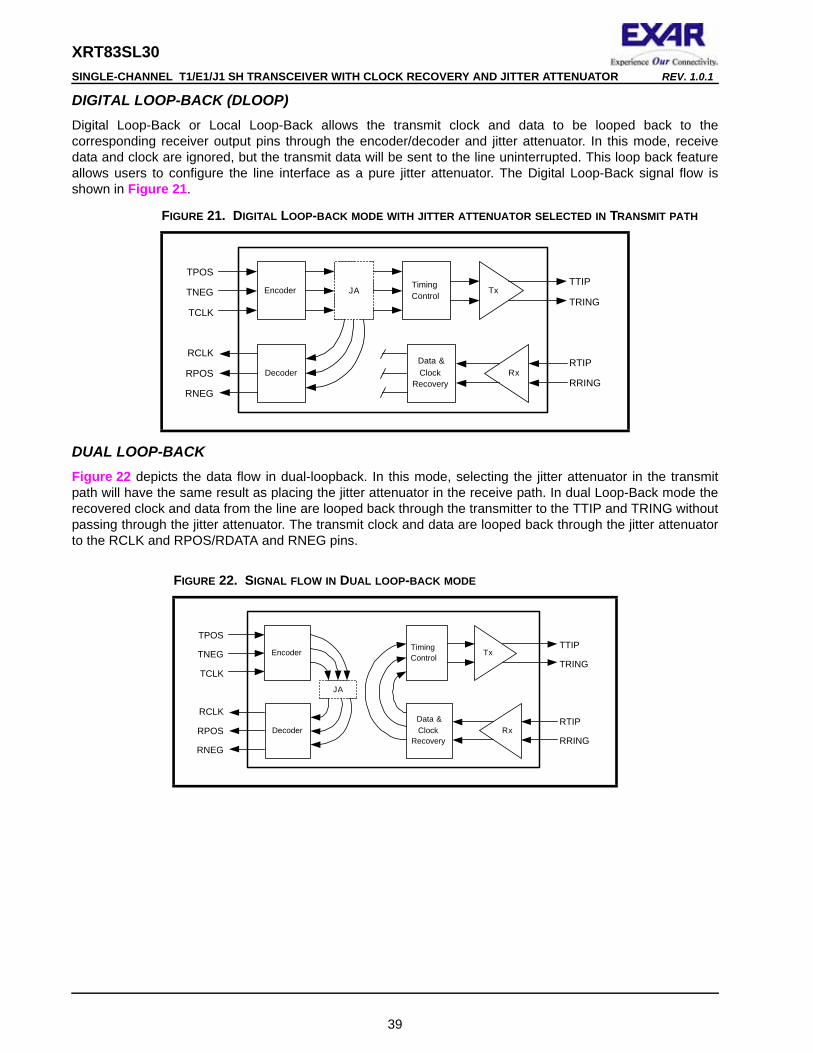
XRT83SL30 SINGLE-CHANNEL T1/E1/J1 SH TRANSCEIVER WITH CLOCK RECOVERY AND JITTER ATTENUATOR REV. 1.0.1
DIGITAL LOOP-BACK (DLOOP)Digital Loop-Back or Local Loop-Back allows the transmit clock and data to be looped back to the corresponding receiver output pins through the encoder/decoder and jitter attenuator. In this mode, receive data and clock are ignored, but the transmit data will be sent to the line uninterrupted. This loop back feature allows users to configure the line interface as a pure jitter attenuator. The Digital Loop-Back signal flow is shown in Figure 21.
DUAL LOOP-BACKFigure 22 depicts the data flow in dual-loopback. In this mode, selecting the jitter attenuator in the transmit path will have the same result as placing the jitter attenuator in the receive path. In dual Loop-Back mode the recovered clock and data from the line are looped back through the transmitter to the TTIP and TRING without passing through the jitter attenuator. The transmit clock and data are looped back through the jitter attenuator to the RCLK and RPOS/RDATA and RNEG pins.
FIGURE 21. DIGITAL LOOP-BACK MODE WITH JITTER ATTENUATOR SELECTED IN TRANSMIT PATH
FIGURE 22. SIGNAL FLOW IN DUAL LOOP-BACK MODE
Tx
Decoder
TimingControl
RxData &Clock
Recovery
JA
TPOS
TNEG
TCLK
RCLK
RPOS
RNEG
EncoderTTIP
TRING
RTIP
RRING
Tx
Decoder
TimingControl
RxData &Clock
Recovery
JA
TPOS
TNEG
TCLK
RCLK
RPOS
RNEG
EncoderTTIP
TRING
RTIP
RRING
39
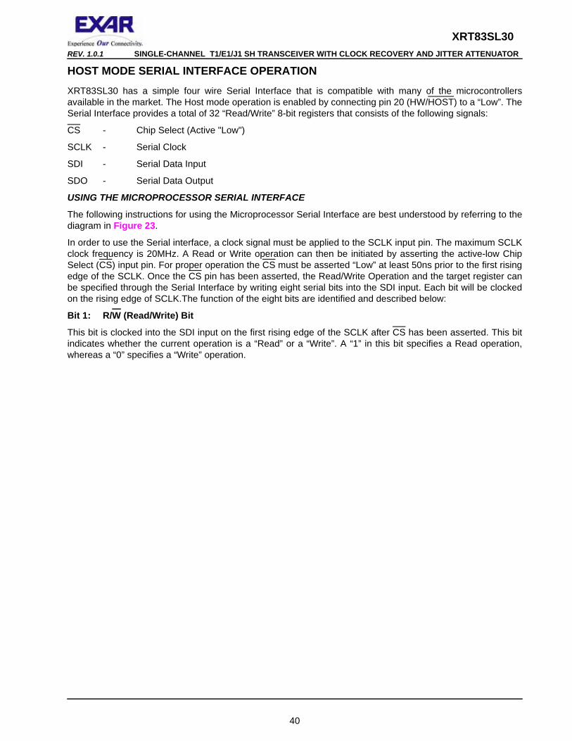
XRT83SL30REV. 1.0.1 SINGLE-CHANNEL T1/E1/J1 SH TRANSCEIVER WITH CLOCK RECOVERY AND JITTER ATTENUATOR
HOST MODE SERIAL INTERFACE OPERATIONXRT83SL30 has a simple four wire Serial Interface that is compatible with many of the microcontrollers available in the market. The Host mode operation is enabled by connecting pin 20 (HW/HOST) to a “Low”. The Serial Interface provides a total of 32 “Read/Write” 8-bit registers that consists of the following signals:
CS - Chip Select (Active "Low")
SCLK - Serial Clock
SDI - Serial Data Input
SDO - Serial Data Output
USING THE MICROPROCESSOR SERIAL INTERFACE
The following instructions for using the Microprocessor Serial Interface are best understood by referring to the diagram in Figure 23.
In order to use the Serial interface, a clock signal must be applied to the SCLK input pin. The maximum SCLK clock frequency is 20MHz. A Read or Write operation can then be initiated by asserting the active-low Chip Select (CS) input pin. For proper operation the CS must be asserted “Low” at least 50ns prior to the first rising edge of the SCLK. Once the CS pin has been asserted, the Read/Write Operation and the target register can be specified through the Serial Interface by writing eight serial bits into the SDI input. Each bit will be clocked on the rising edge of SCLK.The function of the eight bits are identified and described below:
Bit 1: R/W (Read/Write) Bit
This bit is clocked into the SDI input on the first rising edge of the SCLK after CS has been asserted. This bit indicates whether the current operation is a “Read” or a “Write”. A “1” in this bit specifies a Read operation, whereas a “0” specifies a “Write” operation.
40
XRT83SL30 SINGLE-CHANNEL T1/E1/J1 SH TRANSCEIVER WITH CLOCK RECOVERY AND JITTER ATTENUATOR REV. 1.0.1
Bit 2 through 6:The five (5) Address Values (labeled A0, A1, A2, A3 and A4)
The next five rising edges of the SCLK signal, clock in the 5-bit address value for the Read or Write operation. These five bits define the register address within XRT83SL30 that the user has selected to read data from or write data to. The address bits must be supplied to the SDI input in ascending order with LSB (Least Significant Bit) first.
Bit 7: (A5)
The next bit A5 must be set to “0” as shown in Figure 23.
Bit 8: (A6)
The value of A6 is a “don’t care”.
Once the first eight bits have been written into the Serial interface, the subsequent action depends on the whether the current operation is a “Read” or “Write” instruction.
Read Operation
With the last address bit “A4” written into the SDI input, the “Read” operation will proceed through an idle period lasting two SCLK periods. On the rising edge of the 9th SCLK the serial data output (SDO) becomes active (see Figure 23). At this point the user can begin reading the 8-bit data (D0 through D7) stored in the interface register at address [A4,A3,A2,A1,A0], in ascending order (LSB first), on the falling edge of SCLK.
Write Operation
With the last address bit (A4) written into the SDI input, the “Write” operation will proceed through an idle period lasting two SCLK periods. Prior to the rising edge of the 9th SCLK, the user must begin to apply the eight bit data word to the SDI input. The Serial Interface will latch this data on the rising edge of SCLK. The serial data (D0 through D7) should enter the SDI input in ascending order with the LSB first.
Serial Interface Register Description
The serial Interface consists of 32 8-bit register locations. The Microprocessor register address map and Bit map are described in Table 16 and Table 17 respectively. The function of the individual bits are described in Table 18 through Table 36.
FIGURE 23. MICROPROCESSOR SERIAL INTERFACE DATA STRUCTURE
5 6 7 81 2 3 4 13 14 15 169 10 11 12
R/W Ao A1 A2 A3 A4 0 A6 D0 D1 D2 D3 D4 D5 D6 D7
D0 D1 D2 D3 D4 D5 D6 D7
CS
SCLK
SDI
SDO High Z High Z
41
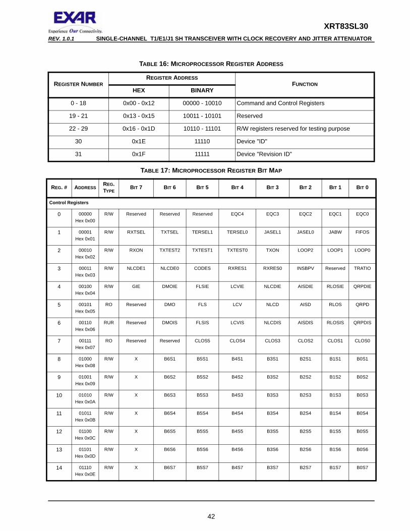
XRT83SL30REV. 1.0.1 SINGLE-CHANNEL T1/E1/J1 SH TRANSCEIVER WITH CLOCK RECOVERY AND JITTER ATTENUATOR
TABLE 16: MICROPROCESSOR REGISTER ADDRESS
REGISTER NUMBERREGISTER ADDRESS
FUNCTIONHEX BINARY
0 - 18 0x00 - 0x12 00000 - 10010 Command and Control Registers
19 - 21 0x13 - 0x15 10011 - 10101 Reserved
22 - 29 0x16 - 0x1D 10110 - 11101 R/W registers reserved for testing purpose
30 0x1E 11110 Device "ID"
31 0x1F 11111 Device "Revision ID"
TABLE 17: MICROPROCESSOR REGISTER BIT MAP
REG. # ADDRESSREG. TYPE
BIT 7 BIT 6 BIT 5 BIT 4 BIT 3 BIT 2 BIT 1 BIT 0
Control Registers
0 00000Hex 0x00
R/W Reserved Reserved Reserved EQC4 EQC3 EQC2 EQC1 EQC0
1 00001Hex 0x01
R/W RXTSEL TXTSEL TERSEL1 TERSEL0 JASEL1 JASEL0 JABW FIFOS
2 00010Hex 0x02
R/W RXON TXTEST2 TXTEST1 TXTEST0 TXON LOOP2 LOOP1 LOOP0
3 00011Hex 0x03
R/W NLCDE1 NLCDE0 CODES RXRES1 RXRES0 INSBPV Reserved TRATIO
4 00100Hex 0x04
R/W GIE DMOIE FLSIE LCVIE NLCDIE AISDIE RLOSIE QRPDIE
5 00101Hex 0x05
RO Reserved DMO FLS LCV NLCD AISD RLOS QRPD
6 00110Hex 0x06
RUR Reserved DMOIS FLSIS LCVIS NLCDIS AISDIS RLOSIS QRPDIS
7 00111Hex 0x07
RO Reserved Reserved CLOS5 CLOS4 CLOS3 CLOS2 CLOS1 CLOS0
8 01000Hex 0x08
R/W X B6S1 B5S1 B4S1 B3S1 B2S1 B1S1 B0S1
9 01001Hex 0x09
R/W X B6S2 B5S2 B4S2 B3S2 B2S2 B1S2 B0S2
10 01010Hex 0x0A
R/W X B6S3 B5S3 B4S3 B3S3 B2S3 B1S3 B0S3
11 01011Hex 0x0B
R/W X B6S4 B5S4 B4S4 B3S4 B2S4 B1S4 B0S4
12 01100Hex 0x0C
R/W X B6S5 B5S5 B4S5 B3S5 B2S5 B1S5 B0S5
13 01101Hex 0x0D
R/W X B6S6 B5S6 B4S6 B3S6 B2S6 B1S6 B0S6
14 01110Hex 0x0E
R/W X B6S7 B5S7 B4S7 B3S7 B2S7 B1S7 B0S7
42
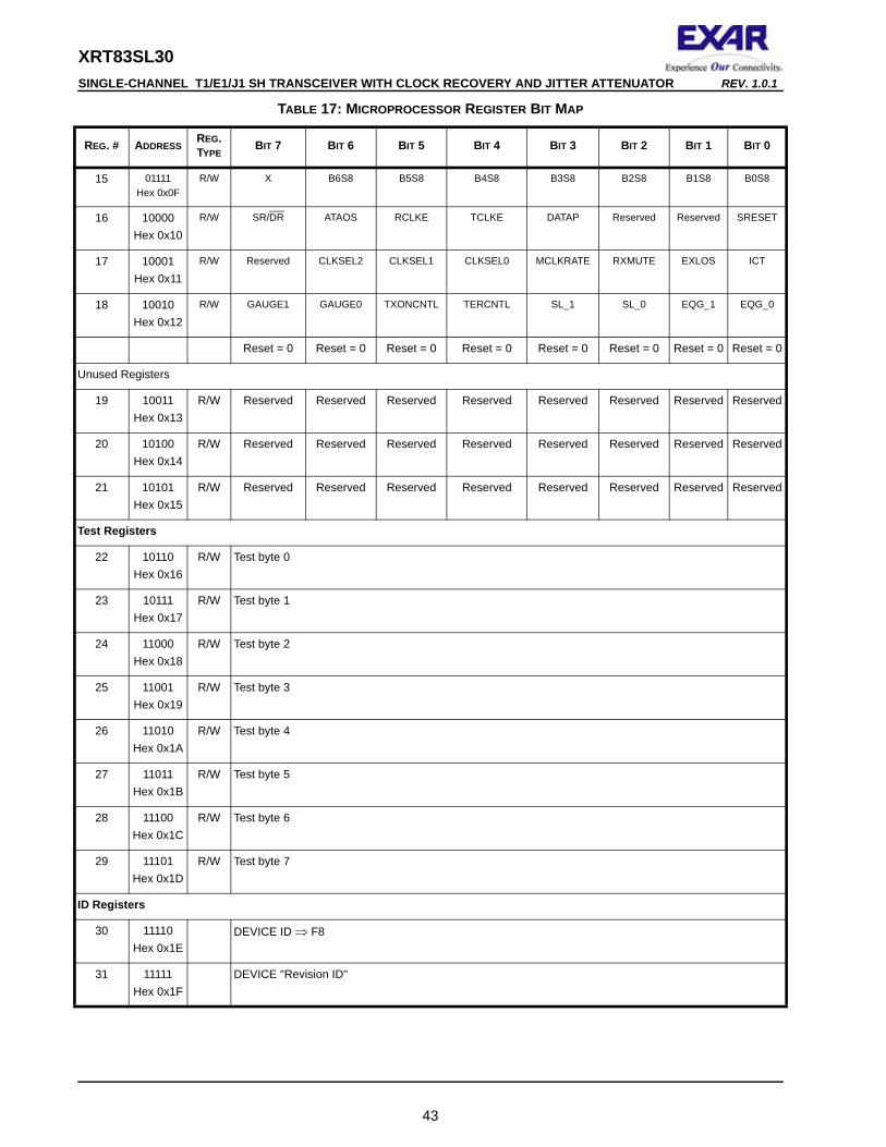
XRT83SL30 SINGLE-CHANNEL T1/E1/J1 SH TRANSCEIVER WITH CLOCK RECOVERY AND JITTER ATTENUATOR REV. 1.0.1
15 01111Hex 0x0F
R/W X B6S8 B5S8 B4S8 B3S8 B2S8 B1S8 B0S8
16 10000Hex 0x10
R/W SR/DR ATAOS RCLKE TCLKE DATAP Reserved Reserved SRESET
17 10001Hex 0x11
R/W Reserved CLKSEL2 CLKSEL1 CLKSEL0 MCLKRATE RXMUTE EXLOS ICT
18 10010Hex 0x12
R/W GAUGE1 GAUGE0 TXONCNTL TERCNTL SL_1 SL_0 EQG_1 EQG_0
Reset = 0 Reset = 0 Reset = 0 Reset = 0 Reset = 0 Reset = 0 Reset = 0 Reset = 0
Unused Registers
19 10011Hex 0x13
R/W Reserved Reserved Reserved Reserved Reserved Reserved Reserved Reserved
20 10100Hex 0x14
R/W Reserved Reserved Reserved Reserved Reserved Reserved Reserved Reserved
21 10101Hex 0x15
R/W Reserved Reserved Reserved Reserved Reserved Reserved Reserved Reserved
Test Registers
22 10110Hex 0x16
R/W Test byte 0
23 10111Hex 0x17
R/W Test byte 1
24 11000Hex 0x18
R/W Test byte 2
25 11001Hex 0x19
R/W Test byte 3
26 11010Hex 0x1A
R/W Test byte 4
27 11011Hex 0x1B
R/W Test byte 5
28 11100Hex 0x1C
R/W Test byte 6
29 11101Hex 0x1D
R/W Test byte 7
ID Registers
30 11110Hex 0x1E
DEVICE ID ⇒ F8
31 11111Hex 0x1F
DEVICE "Revision ID"
TABLE 17: MICROPROCESSOR REGISTER BIT MAP
REG. # ADDRESSREG. TYPE
BIT 7 BIT 6 BIT 5 BIT 4 BIT 3 BIT 2 BIT 1 BIT 0
43
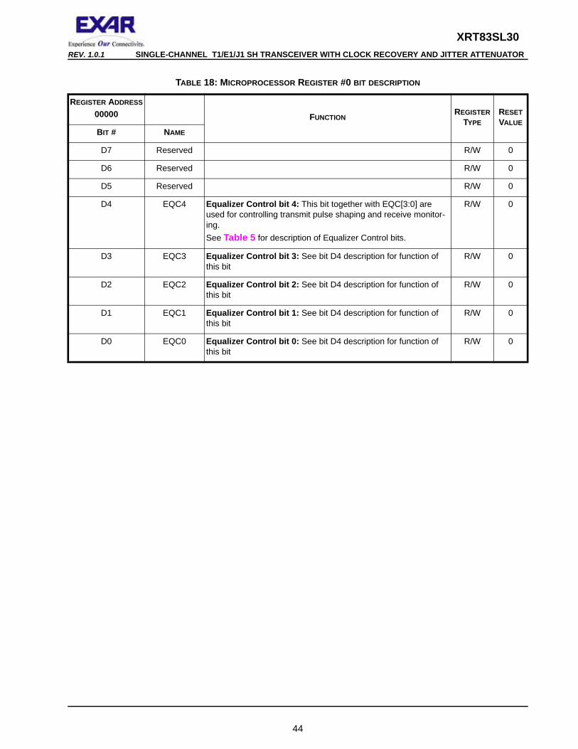
XRT83SL30REV. 1.0.1 SINGLE-CHANNEL T1/E1/J1 SH TRANSCEIVER WITH CLOCK RECOVERY AND JITTER ATTENUATOR
TABLE 18: MICROPROCESSOR REGISTER #0 BIT DESCRIPTION
REGISTER ADDRESS
00000 FUNCTIONREGISTER
TYPERESET VALUE
BIT # NAME
D7 Reserved R/W 0
D6 Reserved R/W 0
D5 Reserved R/W 0
D4 EQC4 Equalizer Control bit 4: This bit together with EQC[3:0] are used for controlling transmit pulse shaping and receive monitor-ing. See Table 5 for description of Equalizer Control bits.
R/W 0
D3 EQC3 Equalizer Control bit 3: See bit D4 description for function of this bit
R/W 0
D2 EQC2 Equalizer Control bit 2: See bit D4 description for function of this bit
R/W 0
D1 EQC1 Equalizer Control bit 1: See bit D4 description for function of this bit
R/W 0
D0 EQC0 Equalizer Control bit 0: See bit D4 description for function of this bit
R/W 0
44
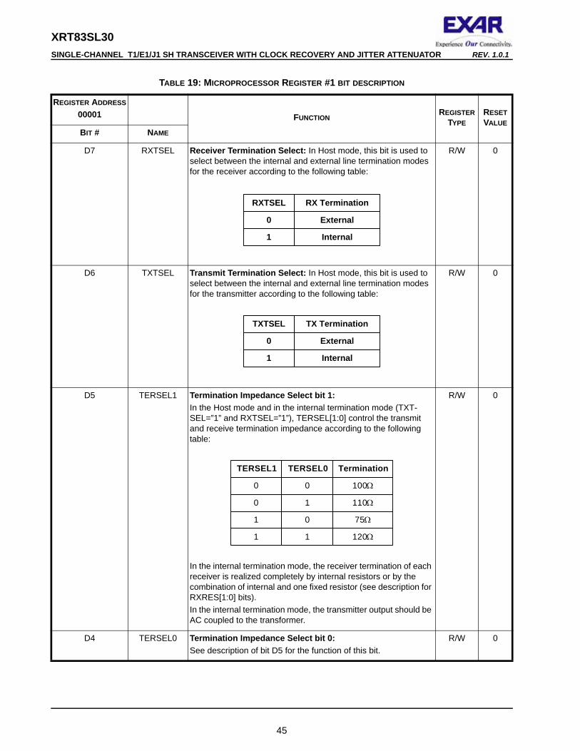
XRT83SL30 SINGLE-CHANNEL T1/E1/J1 SH TRANSCEIVER WITH CLOCK RECOVERY AND JITTER ATTENUATOR REV. 1.0.1
TABLE 19: MICROPROCESSOR REGISTER #1 BIT DESCRIPTION
REGISTER ADDRESS
00001 FUNCTIONREGISTER
TYPERESET VALUE
BIT # NAME
D7 RXTSEL Receiver Termination Select: In Host mode, this bit is used to select between the internal and external line termination modes for the receiver according to the following table:
R/W 0
D6 TXTSEL Transmit Termination Select: In Host mode, this bit is used to select between the internal and external line termination modes for the transmitter according to the following table:
R/W 0
D5 TERSEL1 Termination Impedance Select bit 1:In the Host mode and in the internal termination mode (TXT-SEL=”1” and RXTSEL=”1”), TERSEL[1:0] control the transmit and receive termination impedance according to the following table:
In the internal termination mode, the receiver termination of each receiver is realized completely by internal resistors or by the combination of internal and one fixed resistor (see description for RXRES[1:0] bits).In the internal termination mode, the transmitter output should be AC coupled to the transformer.
R/W 0
D4 TERSEL0 Termination Impedance Select bit 0:See description of bit D5 for the function of this bit.
R/W 0
RXTSEL RX Termination
0
1
External
Internal
TXTSEL TX Termination
0
1
External
Internal
0 1
1 0
1 1
0 0 100Ω
110Ω
75Ω
120Ω
TerminationTERSEL1 TERSEL0
45
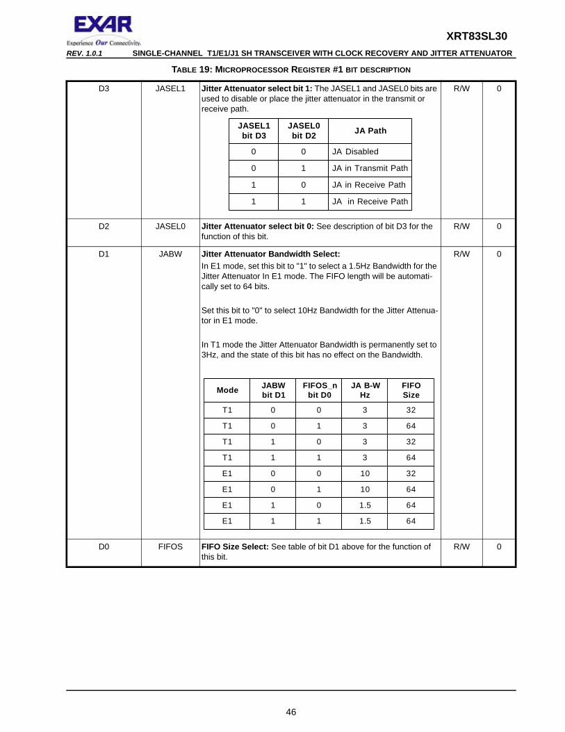
XRT83SL30REV. 1.0.1 SINGLE-CHANNEL T1/E1/J1 SH TRANSCEIVER WITH CLOCK RECOVERY AND JITTER ATTENUATOR
D3 JASEL1 Jitter Attenuator select bit 1: The JASEL1 and JASEL0 bits are used to disable or place the jitter attenuator in the transmit or receive path.
R/W 0
D2 JASEL0 Jitter Attenuator select bit 0: See description of bit D3 for the function of this bit.
R/W 0
D1 JABW Jitter Attenuator Bandwidth Select: In E1 mode, set this bit to "1" to select a 1.5Hz Bandwidth for the Jitter Attenuator In E1 mode. The FIFO length will be automati-cally set to 64 bits.
Set this bit to "0" to select 10Hz Bandwidth for the Jitter Attenua-tor in E1 mode.
In T1 mode the Jitter Attenuator Bandwidth is permanently set to 3Hz, and the state of this bit has no effect on the Bandwidth.
R/W 0
D0 FIFOS FIFO Size Select: See table of bit D1 above for the function of this bit.
R/W 0
TABLE 19: MICROPROCESSOR REGISTER #1 BIT DESCRIPTION
JASEL1bit D3
JASEL0bit D2
0 0
0 1
1 0
1 1
JA Path
JA Disabled
JA in Transmit Path
JA in Receive Path
JA in Receive Path
0
1
0
1
0
1
0
1
FIFOS_nbit D0
0
0
1
1
0
0
1
1
JABWbit D1
T1
T1
T1
T1
E1
E1
E1
E1
Mode
32
64
32
64
32
64
64
64
FIFOSize
3
3
3
3
10
10
1.5
1.5
JA B-WHz
46
XRT83SL30 SINGLE-CHANNEL T1/E1/J1 SH TRANSCEIVER WITH CLOCK RECOVERY AND JITTER ATTENUATOR REV. 1.0.1
TABLE 20: MICROPROCESSOR REGISTER #2 BIT DESCRIPTION
REGISTER ADDRESS
00010 FUNCTIONREGISTER
TYPERESET VALUE
BIT # NAME
D7 RXON Receiver ON: Writing a “1” into this bit location turns on the Receive Section. Writing a “0” shuts off the Receiver Section. In this mode, RTIP and RRING driver outputs will be tri-stated for power reduction or redundancy applications. Default is "0", off.
R/W 0
D6 TXTEST2 Transmit Test Pattern bit 2: This bit together with TXTEST1 and TXTEST0 are used to generate and transmit test patterns according to the following table:
TDQRSS (Transmit/Detect Quasi-Random Signal): This con-dition, when activated, enables Quasi-Random Signal Source generation and detection. In a T1 system QRSS pattern is a 220-1 pseudo-random bit sequence (PRBS) with no more than 14 consecutive zeros. In a E1 system, QRSS is a 215-1 PRBS pat-tern.
TAOS (Transmit All Ones): Activating this condition enables the transmission of an All Ones Pattern. TCLK must not be tied "Low".
TLUC (Transmit Network Loop-Up Code): Activating this con-dition enables the Network Loop-Up Code of "00001" to be trans-mitted to the line. When Network Loop-Up code is being transmitted, the XRT83SL30 will ignore the Automatic Loop-Code detection and Remote Loop-Back activation (NLCDE1 =“1”, NLCDE0 =“1”, if activated) in order to avoid activating Remote Digital Loop-Back automatically when the remote termi-nal responds to the Loop-Back request.
TLDC (Transmit Network LOOP-Down Code): Activating this condition enables the network Loop-Down Code of "001" to be transmitted to the line.
R/W 0
D5 TXTEST1 Transmit Test pattern bit 1: See description of bit D6 for the function of this bit.
R/W 0
D4 TXTEST0 Transmit Test Pattern bit 0: See description of bit D6 for the function of this bit.
R/W 0
0 1
1 0
1 1
0 0
0
0
0
1
0 00 Transmit Data
TAOS
TLUC
TLDC
Test PatternTXTEST1 TXTEST0TXTEST2
1 0
1 1
1
1
0 11
TDQRSS
TDQRSS & INVQRSS
TDQRSS & INSBER
TDQRSS & INVQRSS & INS
47
XRT83SL30REV. 1.0.1 SINGLE-CHANNEL T1/E1/J1 SH TRANSCEIVER WITH CLOCK RECOVERY AND JITTER ATTENUATOR
D3 TXON Transmitter ON: Writing a "1" into this bit location turns on the Transmit Section. A ‘0’ in this bit location, shuts off the transmit-ter. In this mode the TTIP and TRING driver outputs will be tri-stated for power reduction or redundancy applications.
R/W 0
D2 LOOP2 Loop-Back control bit 2: This bit together with the LOOP1 and LOOP0 bits control the Loop-Back modes of the chip according to the following table:
R/W 0
D1 LOOP1 Loop-Back control bit 1: See description of bit D2 for the func-tion of this bit.
R/W 0
D0 LOOP0 Loop-Back control bit 0: See description of bit D2 for the func-tion of this bit.
R/W 0
TABLE 20: MICROPROCESSOR REGISTER #2 BIT DESCRIPTION
LOOP2
0
1
1
1
1
LOOP1
X
0
0
1
1
LOOP0
X
0
1
0
1
Loop-Back Mode
No Loop-Back
Dual Loop-Back
Analog Loop-Back
Remote Loop-Back
Digital Loop-Back
48
XRT83SL30 SINGLE-CHANNEL T1/E1/J1 SH TRANSCEIVER WITH CLOCK RECOVERY AND JITTER ATTENUATOR REV. 1.0.1
TABLE 21: MICROPROCESSOR REGISTER #3 BIT DESCRIPTION
REGISTER ADDRESS
00011 FUNCTIONREGISTER
TYPERESET VALUE
BIT # NAME
D7 NLCDE1 Network Loop Code Detection Enable bit 1:This bit together with NLCDE0, Control the Loop-Code detection according to the following table:
When NLCDE1=”0” and NCLDE0=”1”, or NLCDE1=”1” and NLCDE0=”0”, the chip is manually programed to monitor the receive data for the Loop-Up or Loop-Down code respectively. When the presence of the “00001” or “001” pattern is detected for more than 5 seconds, the status of the NLCD bit is set to “1” and if the NLCD interrupt is enabled an interrupt is initiated. The Host has the option to control the Loop-Back function manually.Setting the NLCDE1=”1” and NLCDE0=”1” enables the Auto-matic Loop-Code detection and Remote-Loop-Back activation mode. As this mode is initiated, the state of the NLCD interface bit is reset to “0” and the chip is programmed to monitor the receive data for the Loop-Up Code. If the “00001” pattern is detected for longer than 5 seconds, the NLCD bit is set to “1”, Remote Loop-Back is activated and the chip is automatically pro-gramed to monitor the receive data for the Loop-Down code. The NLCD bit stays set even after the chip stops receiving the Loop-Up code. The remote Loop-Back condition is removed when the chip receives the Loop-Down code for more than 5 seconds or if the Automatic Loop-Code detection mode is terminated.
R/WR/W
00
D6 NLCDE0 Network Loop Code Detection Enable bit 0: See description of bit D7 for the function of this bit.
R/W 0
D5 CODES ENCODING and DECODING SELECT:Writing a “0” to this bit selects HDB3 or B8ZS encoding and decoding. Writing a “1” selects an AMI coding scheme.This bit is only active when single-rail mode is selected.
R/W 0
NLCDE1 NLCDE0 Function
0 0 Disable Loop-CodeDetection
0 1 Detect Loop-Up Code inReceive Data
1 1 Automatic Loop-CodeDetection
1 0 Detect Loop-Down Code inReceive Data
49
XRT83SL30REV. 1.0.1 SINGLE-CHANNEL T1/E1/J1 SH TRANSCEIVER WITH CLOCK RECOVERY AND JITTER ATTENUATOR
D4 RXRES1 Receive External Resistor Control pin 1: In Host mode, this bit along with the RXRES0 bit selects the value of the external Receive fixed resistor according to the following table:
R/W 0
D3 RXRES0 Receive External Resistor Control bit 0: For function of this bit see description of D4 the RXRES1 bit.
R/W 0
D2 INSBPV Insert Bipolar Violation: When this bit transitions from "0" to "1", a bipolar violation is inserted in the transmitted data stream. Bipolar violation can be inserted either in the QRSS pattern, or input data when operating in single-rail mode. The state of this bit is sampled on the rising edge of TCLK. NOTE: To ensure the insertion of a bipolar violation, a "0" should
be written in this bit location before writing a "1".
R/W 0
D1 Reserved R/W 0
D0 TRATIO Transformer Ratio Select: In the external termination mode, writing a “1” to this bit selects a transformer ratio of 1:2 for the transmitter. Writing a “0” sets the transmitter transformer ratio to 1: 2.45. In the internal termination mode the transmitter trans-former ratio is permanently set to 1:2 and the state of this bit has no effect.
R/W 0
TABLE 21: MICROPROCESSOR REGISTER #3 BIT DESCRIPTION
Required Fixed ExternalRX Resistor
No External Fixed Resistor
60Ω
52.5Ω
37.5Ω
RXRES0
0
1
0
1
RXRES1
0
0
1
1
50
XRT83SL30 SINGLE-CHANNEL T1/E1/J1 SH TRANSCEIVER WITH CLOCK RECOVERY AND JITTER ATTENUATOR REV. 1.0.1
TABLE 22: MICROPROCESSOR REGISTER #4 BIT DESCRIPTION
REGISTER ADDRESS
00100 FUNCTIONREGISTER
TYPERESET VALUE
BIT # NAME
D7 GIE Global Interrupt Enable: Writing a "1" into this bit, globally enables interrupt generation on the INT pin. Writing a "0" into this bit, globally masks all interrupt requests.
R/W 0
D6 DMOIE DMO Interrupt Enable: Writing a "1" to this bit enables DMO interrupt generation, writing a "0" masks it.
R/W 0
D5 FLSIE FIFO Limit Status Interrupt Enable: Writing a "1" to this bit enables interrupt generation when the FIFO limit is within 3 bits, writing a "0" to masks it.
R/W 0
D4 LCVIE Line Code Violation Interrupt Enable: Writing a "1" to this bit enables Line Code Violation interrupt generation, writing a "0" masks it.
R/W 0
D3 NLCDIE Network Loop-Code Detection Interrupt Enable: Writing a "1" to this bit enables Network Loop-code detection interrupt genera-tion, writing a "0" masks it.
R/W 0
D2 AISDIE AIS Detection Interrupt Enable: Writing a "1" to this bit enables Alarm Indication Signal detection interrupt generation, writing a "0" masks it.
R/W 0
D1 RLOSIE Receive Loss of Signal Interrupt Enable: Writing a "1" to this bit enables Loss of Receive Signal interrupt generation, writing a "0" masks it.
R/W 0
D0 QRPDIE QRSS Pattern Detection Interrupt Enable: Writing a "1" to this bit enables QRSS pattern detection interrupt generation, writing a "0" masks it.
R/W 0
51
XRT83SL30REV. 1.0.1 SINGLE-CHANNEL T1/E1/J1 SH TRANSCEIVER WITH CLOCK RECOVERY AND JITTER ATTENUATOR
TABLE 23: MICROPROCESSOR REGISTER #5 BIT DESCRIPTION
REGISTER ADDRESS
00101 FUNCTIONREGISTER
TYPERESET VALUE
BIT # NAME
D7 Reserved RO 0
D6 DMO Driver Monitor Output: This bit is set to a "1" to indicate trans-mit driver failure is detected. The value of this bit is based on the current status of DMO. If the DMOIE bit is enabled, any transition on this bit will generate an Interrupt.
RO 0
D5 FLS FiFO Limit Status: This bit is set to a "1" to indicate that the jitter attenuator read/write FIFO pointers are within +/- 3 bits. If the FLSIE bit is enabled, any transition on this bit will generate an Interrupt.
RO 0
D4 LCV Line Code Violation: This bit is set to a "1" to indicate that the receiver is currently detecting a Line Code Violation or an exces-sive number of zeros in the B8ZS or HDB3 modes. If the LCVIE bit is enabled, any transition on this bit will generate an Interrupt.
RO 0
52
XRT83SL30 SINGLE-CHANNEL T1/E1/J1 SH TRANSCEIVER WITH CLOCK RECOVERY AND JITTER ATTENUATOR REV. 1.0.1
D3 NLCD Network Loop-Code Detection:This bit operates differently in the Manual or the Automatic Net-work Loop-Code detection modes.
In the Manual Loop-Code detection mode (NLCDE1 =”0” and NLCDE0 =”1”, or NLCDE1 =”1” and NLCDE0 =”0”) this bit gets set to “1” as soon as the Loop-Up (“00001”) or Loop-Down (“001”) code is detected in the receive data for longer than 5 sec-onds. The NLCD bit stays in the “1” state for as long as the chip detects the presence of the Loop-Code in the receive data and it is reset to “0” as soon as it stops receiving it. In this mode if the NLCD interrupt is enabled the chip will initiate an interrupt on every transition of the NLCD.
When the Automatic Loop-Code detection mode (NLCDE1 =”1” and NLCDE0 =”1”) is initiated, the state of the NLCD interface bit is reset to “0” and the chip is programmed to monitor the receive input data for the Loop-Up Code. This bit is set to a “1” to indicate that the Network Loop Code is detected for more than 5 sec-onds. Simultaneously the Remote Loop-Back condition is auto-matically activated and the chip is programmed to monitor the receive data for the Network Loop-Down Code. The NLCD bit stays in the “1” state for as long as the Remote Loop-Back condi-tion is in effect even if the chip stops receiving the Loop-Up Code. Remote Loop-Back is removed if the chip detects the “001” pattern for longer than 5 seconds in the receive data. Detecting the “001” pattern also results in resetting the NLCD interface bit and initiating an interrupt provided the NLCD inter-rupt enable bit it active. When programmed in the Automatic detection mode, the NLCD interface bit stays “High” for the entire time the Remote Loop-Back is active and initiates an interrupt anytime the status of the NLCD bit changes. In this mode the host can monitor the state of the NLCD bit to determine if the Remote Loop-Back is activated.
RO 0
D2 AISD Alarm Indication Signal Detect: This bit is set to a "1" to indi-cate All Ones Signal is detected by the receiver. The value of this bit is based on the current status of Alarm Indication Signal detector. If the AISDIE bit is enabled, any transition on this bit will generate an Interrupt.
RO 0
D1 RLOS Receive Loss of Signal: This bit is set to a "1" to indicate that the receive input signal is lost. The value of this bit is based on the current status of the receive input signal. If the RLOSIE bit is enabled, any transition on this bit will generate an Interrupt.
RO 0
D0 QRPD Quasi-random Pattern Detection: This bit is set to a "1" to indi-cate the receiver is currently in synchronization with QRSS pat-tern. The value of this bit is based on the current status of Quasi-random pattern detector of. If the QRPDIE bit is enabled, any transition on this bit will generate an Interrupt.
RO 0
TABLE 23: MICROPROCESSOR REGISTER #5 BIT DESCRIPTION
53
XRT83SL30REV. 1.0.1 SINGLE-CHANNEL T1/E1/J1 SH TRANSCEIVER WITH CLOCK RECOVERY AND JITTER ATTENUATOR
TABLE 24: MICROPROCESSOR REGISTER #6 BIT DESCRIPTION
REGISTER ADDRESS
00110 FUNCTIONREGISTER
TYPERESET VALUE
BIT # NAME
D7 Reserved RUR 0
D6 DMOIS Driver Monitor Output Interrupt Status: This bit is set to a "1" every time when DMO status has changed since last read.
RUR 0
D5 FLSIS FIFO Limit Interrupt Status: This bit is set to a "1" every time when FIFO Limit (Read/Write pointer with +/- 3 bits apart) status has changed since last read.
RUR 0
D4 LCVIS Line Code Violation Interrupt Status: This bit is set to a "1" every time when LCV status has changed since last read.
RUR 0
D3 NLCDIS Network Loop-Code Detection Interrupt Status: This bit is set to a "1" every time when NLCD status has changed since last read.
RUR 0
D2 AISDIS AIS Detection Interrupt Status: This bit is set to a "1" every time when AISD status has changed since last read.
RUR 0
D1 RLOSIS Receive Loss of Signal Interrupt Status: This bit is set to a "1" every time RLOS status has changed since last read.
RUR 0
D0 QRPDIS Quasi-Random Pattern Detection Interrupt Status: This bit is set to a "1" every time when QRPD status has changed since last read.
RUR 0
54
XRT83SL30 SINGLE-CHANNEL T1/E1/J1 SH TRANSCEIVER WITH CLOCK RECOVERY AND JITTER ATTENUATOR REV. 1.0.1
TABLE 25: MICROPROCESSOR REGISTER #7 BIT DESCRIPTION
REGISTER ADDRESS
00111 FUNCTIONREGISTER
TYPERESET VALUE
BIT # NAME
D7 Reserved RO 0
D6 Reserved RO 0
D5 CLOS5 Cable Loss bit 5: CLOS[5:0] are the six bits receiver for selec-tive equalizer setting which is also a binary word that represents the cable attenuation indication within ±1dB. CLOS5 is the most significant bit (MSB) and CLOS0 is the least significant bit (LSB).
RO 0
D4 CLOS4 Cable Loss bit 4: See description of D5 for function of this bit. RO 0
D3 CLOS3 Cable Loss bit 3: See description of D5 for function of this bit. RO 0
D2 CLOS2 Cable Loss bit 2: See description of D5 for function of this bit. RO 0
D1 CLOS1 Cable Loss bit 1: See description of D5 for function of this bit. RO 0
D0 CLOS0 Cable Loss bit 0: See description of D5 for function of this bit. RO 0
TABLE 26: MICROPROCESSOR REGISTER #8 BIT DESCRIPTION
REGISTER ADDRESS
01000 FUNCTIONREGISTER
TYPERESET VALUE
BIT # NAME
D7 Reserved R/W 0
D6-D0 B6S1 - B0S1 Arbitrary Transmit Pulse Shape, Segment 1The shape of the transmitted pulse can be made user program-mable by selecting "Arbitrary Pulse" mode, see Table 5. The arbitrary pulse is divided into eight time segments whose com-bined duration is equal to one period of MCLK.This 7 bit number represents the amplitude of the arbitrary pulse during the first time segment. B6S1 -B0S1 is in signed magni-tude format with B6S1 as the sign bit and B0S1 as the least sig-nificant bit (LSB).
R/W 0
55

XRT83SL30REV. 1.0.1 SINGLE-CHANNEL T1/E1/J1 SH TRANSCEIVER WITH CLOCK RECOVERY AND JITTER ATTENUATOR
TABLE 27: MICROPROCESSOR REGISTER #9 BIT DESCRIPTION
REGISTER ADDRESS
01001 FUNCTIONREGISTER
TYPERESET VALUE
BIT # NAME
D7 Reserved R/W 0
D6-D0 B6S2 - B0S2 Arbitrary Transmit Pulse Shape, Segment 2The shape of the transmitted pulse can be made user program-mable by selecting "Arbitrary Pulse" mode, see Table 5. The arbitrary pulse is divided into eight time segments whose com-bined duration is equal to one period of MCLK.This 7 bit number represents the amplitude of the arbitrary pulse during the second time segment. B6S2 -B0S2 is in signed mag-nitude format with B6S2 as the sign bit and B0S2 as the least significant bit (LSB).
R/W 0
TABLE 28: MICROPROCESSOR REGISTER #10 BIT DESCRIPTION
REGISTER ADDRESS
01010 FUNCTIONREGISTER
TYPERESET VALUE
BIT # NAME
D7 Reserved R/W 0
D6-D0 B6S3 - B0S3 Arbitrary Transmit Pulse Shape, Segment 3The shape of the transmitted pulse can be made user program-mable by selecting "Arbitrary Pulse" mode, see Table 5. The arbitrary pulse is divided into eight time segments whose com-bined duration is equal to one period of MCLK.This 7 bit number represents the amplitude of the arbitrary pulse during the third time segment. B6S3 -B0S3 is in signed magni-tude format with B6S3 as the sign bit and B0S3 as the least sig-nificant bit (LSB).
R/W 0
56
XRT83SL30 SINGLE-CHANNEL T1/E1/J1 SH TRANSCEIVER WITH CLOCK RECOVERY AND JITTER ATTENUATOR REV. 1.0.1
TABLE 29: MICROPROCESSOR REGISTER #11 BIT DESCRIPTION
REGISTER ADDRESS
01011 FUNCTIONREGISTER
TYPERESET VALUE
BIT # NAME
D7 Reserved R/W 0
D6-D0 B6S4 - B0S4 Arbitrary Transmit Pulse Shape, Segment 4The shape of the transmitted pulse can be made user program-mable by selecting "Arbitrary Pulse" mode, see Table 5. The arbitrary pulse is divided into eight time segments whose com-bined duration is equal to one period of MCLK.This 7 bit number represents the amplitude of the arbitrary pulse during the fourth time segment. B6S4 -B0S4 is in signed magni-tude format with B6S4 as the sign bit and B0S4 as the least sig-nificant bit (LSB).
R/W 0
TABLE 30: MICROPROCESSOR REGISTER #12 BIT DESCRIPTION
REGISTER ADDRESS
01100 FUNCTIONREGISTER
TYPERESET VALUE
BIT # NAME
D7 Reserved R/W 0
D6-D0 B6S5 - B0S5 Arbitrary Transmit Pulse Shape, Segment 5The shape of the transmitted pulse can be made user program-mable by selecting "Arbitrary Pulse" mode, see Table 5. The arbitrary pulse is divided into eight time segments whose com-bined duration is equal to one period of MCLK.This 7 bit number represents the amplitude of the arbitrary pulse during the fifth time segment. B6S5 -B0S5 is in signed magni-tude format with B6S5 as the sign bit and B0S5 as the least sig-nificant bit (LSB).
R/W 0
57
XRT83SL30REV. 1.0.1 SINGLE-CHANNEL T1/E1/J1 SH TRANSCEIVER WITH CLOCK RECOVERY AND JITTER ATTENUATOR
TABLE 31: MICROPROCESSOR REGISTER #13 BIT DESCRIPTION
REGISTER ADDRESS
01101 FUNCTIONREGISTER
TYPERESET VALUE
BIT # NAME
D7 Reserved R/W 0
D6-D0 B6S6 - B0S6 Arbitrary Transmit Pulse Shape, Segment 6The shape of the transmitted pulse can be made user program-mable by selecting "Arbitrary Pulse" mode, see Table 5. The arbitrary pulse is divided into eight time segments whose com-bined duration is equal to one period of MCLK.This 7 bit number represents the amplitude of the arbitrary pulse during the sixth time segment. B6S6 -B0S6 is in signed magni-tude format with B6S6 as the sign bit and B0S6 as the least sig-nificant bit (LSB).
R/W 0
TABLE 32: MICROPROCESSOR REGISTER #14 BIT DESCRIPTION
REGISTER ADDRESS
01110 FUNCTIONREGISTER
TYPERESET VALUE
BIT # NAME
D7 Reserved R/W 0
D6-D0 B6S7 - B0S7 Arbitrary Transmit Pulse Shape, Segment 7The shape of the transmitted pulse can be made user program-mable by selecting "Arbitrary Pulse" mode, see Table 5. The arbitrary pulse is divided into eight time segments whose com-bined duration is equal to one period of MCLK.This 7 bit number represents the amplitude of the arbitrary pulse during the seventh time segment. B6S7 -B0S7 is in signed mag-nitude format with B6S7 as the sign bit and B0S7 as the least significant bit (LSB).
R/W 0
58
XRT83SL30 SINGLE-CHANNEL T1/E1/J1 SH TRANSCEIVER WITH CLOCK RECOVERY AND JITTER ATTENUATOR REV. 1.0.1
TABLE 33: MICROPROCESSOR REGISTER #15 BIT DESCRIPTION
REGISTER ADDRESS
01111 FUNCTIONREGISTER
TYPERESET VALUE
BIT # NAME
D7 Reserved R/W 0
D6-D0 B6S8 - B0S8 Arbitrary Transmit Pulse Shape, Segment 8The shape of the transmitted pulse can be made user program-mable by selecting "Arbitrary Pulse" mode, see Table 5. The arbitrary pulse is divided into eight time segments whose com-bined duration is equal to one period of MCLK.This 7 bit number represents the amplitude of the arbitrary pulse during the eighth time segment. B6S8 -B0S8 is in signed magni-tude format with B6S8 as the sign bit and B0S8 as the least sig-nificant bit (LSB).
R/W 0
59
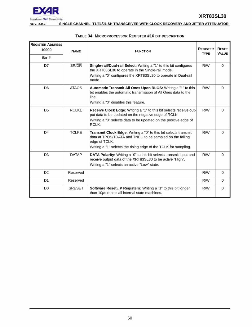
XRT83SL30REV. 1.0.1 SINGLE-CHANNEL T1/E1/J1 SH TRANSCEIVER WITH CLOCK RECOVERY AND JITTER ATTENUATOR
TABLE 34: MICROPROCESSOR REGISTER #16 BIT DESCRIPTION
REGISTER ADDRESS
10000 NAME FUNCTIONREGISTER
TYPERESET VALUE
BIT #
D7 SR/DR Single-rail/Dual-rail Select: Writing a "1" to this bit configures the XRT83SL30 to operate in the Single-rail mode.Writing a "0" configures the XRT83SL30 to operate in Dual-rail mode.
R/W 0
D6 ATAOS Automatic Transmit All Ones Upon RLOS: Writing a "1" to this bit enables the automatic transmission of All Ones data to the line.Writing a "0" disables this feature.
R/W 0
D5 RCLKE Receive Clock Edge: Writing a "1" to this bit selects receive out-put data to be updated on the negative edge of RCLK.Writing a "0" selects data to be updated on the positive edge of RCLK.
R/W 0
D4 TCLKE Transmit Clock Edge: Writing a "0" to this bit selects transmit data at TPOS/TDATA and TNEG to be sampled on the falling edge of TCLK.Writing a "1" selects the rising edge of the TCLK for sampling.
R/W 0
D3 DATAP DATA Polarity: Writing a "0" to this bit selects transmit input and receive output data of the XRT83SL30 to be active "High".Writing a "1" selects an active "Low" state.
R/W 0
D2 Reserved R/W 0
D1 Reserved R/W 0
D0 SRESET Software Reset µP Registers: Writing a "1" to this bit longer than 10µs resets all internal state machines.
R/W 0
60
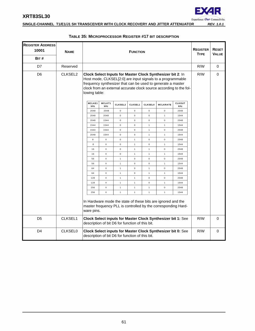
XRT83SL30 SINGLE-CHANNEL T1/E1/J1 SH TRANSCEIVER WITH CLOCK RECOVERY AND JITTER ATTENUATOR REV. 1.0.1
TABLE 35: MICROPROCESSOR REGISTER #17 BIT DESCRIPTION
REGISTER ADDRESS
10001 NAME FUNCTIONREGISTER
TYPERESET VALUE
BIT #
D7 Reserved R/W 0
D6 CLKSEL2 Clock Select Inputs for Master Clock Synthesizer bit 2: In Host mode, CLKSEL[2:0] are input signals to a programmable frequency synthesizer that can be used to generate a master clock from an external accurate clock source according to the fol-lowing table:
In Hardware mode the state of these bits are ignored and the master frequency PLL is controlled by the corresponding Hard-ware pins.
R/W 0
D5 CLKSEL1 Clock Select inputs for Master Clock Synthesizer bit 1: See description of bit D6 for function of this bit.
R/W 0
D4 CLKSEL0 Clock Select inputs for Master Clock Synthesizer bit 0: See description of bit D6 for function of this bit.
R/W 0
2048
2048
2048
1544
MCLKE1kHz
8
16
16
56
8
56
64
64
128
256
256
128
2048
2048
1544
1544
MCLKT1kHz
1544
X
X
X
1544
X
X
X
X
X
X
X
2048
1544
2048
CLKOUTkHz
1544
2048
1544
2048
1544
2048
1544
2048
1544
2048
1544
2048
1544
0
0
1
1
CLKSEL0
0
1
1
0
0
0
1
1
0
1
1
0
0
0
0
0
CLKSEL1
1
1
1
0
1
0
0
0
1
1
1
1
0
0
0
0
CLKSEL2
0
0
0
1
0
1
1
1
1
1
1
1
0
1
0
0
0
0
1544
2048
X
X
2048
1544
0
1
0
1
MCLKRATE
1
0
1
0
0
1
0
1
1
0
1
0
0
1
61
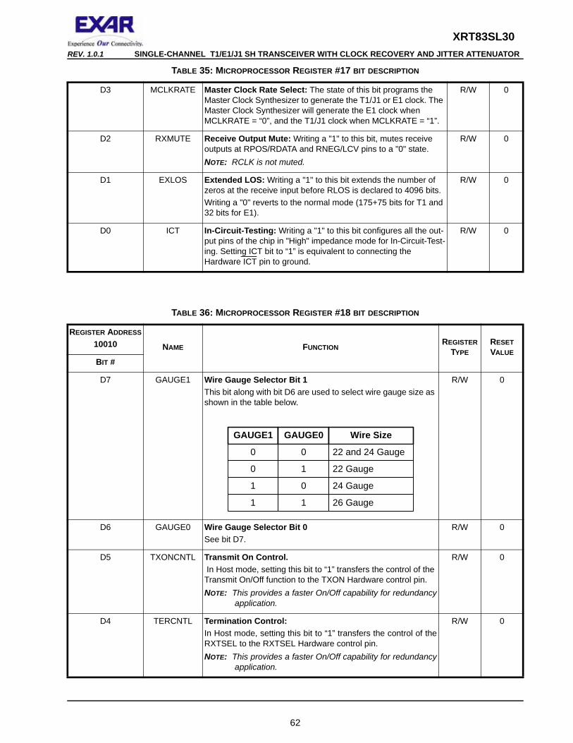
XRT83SL30REV. 1.0.1 SINGLE-CHANNEL T1/E1/J1 SH TRANSCEIVER WITH CLOCK RECOVERY AND JITTER ATTENUATOR
D3 MCLKRATE Master Clock Rate Select: The state of this bit programs the Master Clock Synthesizer to generate the T1/J1 or E1 clock. The Master Clock Synthesizer will generate the E1 clock when MCLKRATE = “0”, and the T1/J1 clock when MCLKRATE = “1”.
R/W 0
D2 RXMUTE Receive Output Mute: Writing a "1" to this bit, mutes receive outputs at RPOS/RDATA and RNEG/LCV pins to a "0" state. NOTE: RCLK is not muted.
R/W 0
D1 EXLOS Extended LOS: Writing a "1" to this bit extends the number of zeros at the receive input before RLOS is declared to 4096 bits.Writing a "0" reverts to the normal mode (175+75 bits for T1 and 32 bits for E1).
R/W 0
D0 ICT In-Circuit-Testing: Writing a "1" to this bit configures all the out-put pins of the chip in "High" impedance mode for In-Circuit-Test-ing. Setting ICT bit to “1” is equivalent to connecting the Hardware ICT pin to ground.
R/W 0
TABLE 36: MICROPROCESSOR REGISTER #18 BIT DESCRIPTION
REGISTER ADDRESS
10010 NAME FUNCTIONREGISTER
TYPERESET VALUE
BIT #
D7 GAUGE1 Wire Gauge Selector Bit 1This bit along with bit D6 are used to select wire gauge size as shown in the table below.
R/W 0
D6 GAUGE0 Wire Gauge Selector Bit 0See bit D7.
R/W 0
D5 TXONCNTL Transmit On Control. In Host mode, setting this bit to “1” transfers the control of the Transmit On/Off function to the TXON Hardware control pin.NOTE: This provides a faster On/Off capability for redundancy
application.
R/W 0
D4 TERCNTL Termination Control:In Host mode, setting this bit to “1” transfers the control of the RXTSEL to the RXTSEL Hardware control pin.NOTE: This provides a faster On/Off capability for redundancy
application.
R/W 0
TABLE 35: MICROPROCESSOR REGISTER #17 BIT DESCRIPTION
GAUGE1
0
1
1
0
GAUGE0
0
1
0
1
Wire Size
22 and 24 Gauge
26 Gauge
24 Gauge
22 Gauge
62
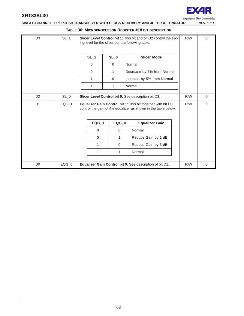
XRT83SL30 SINGLE-CHANNEL T1/E1/J1 SH TRANSCEIVER WITH CLOCK RECOVERY AND JITTER ATTENUATOR REV. 1.0.1
D3 SL_1 Slicer Level Control bit 1: This bit and bit D2 control the slic-ing level for the slicer per the following table.
R/W 0
D2 SL_0 Slicer Level Control bit 0: See description bit D3. R/W 0
D1 EQG_1 Equalizer Gain Control bit 1: This bit together with bit D0 control the gain of the equalizer as shown in the table below.
R/W 0
D0 EQG_0 Equalizer Gain Control bit 0: See description of bit D1. R/W 0
TABLE 36: MICROPROCESSOR REGISTER #18 BIT DESCRIPTION
SL_1 SL_0
0 0
0 1
1 0
1 1
Slicer Mode
Normal
Decrease by 5% from Normal
Increase by 5% from Normal
Normal
EQG_1 EQG_0
0 0
0 1
1 0
1 1
Equalizer Gain
Normal
Reduce Gain by 1 dB
Reduce Gain by 3 dB
Normal
63
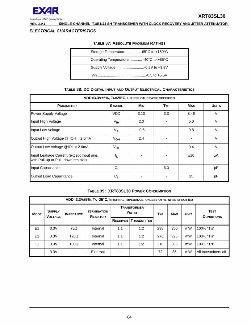
XRT83SL30REV. 1.0.1 SINGLE-CHANNEL T1/E1/J1 SH TRANSCEIVER WITH CLOCK RECOVERY AND JITTER ATTENUATOR
ELECTRICAL CHARACTERISTICS
TABLE 37: ABSOLUTE MAXIMUM RATINGS
Storage Temperature...............-65°C to +150°C
Operating Temperature............. -40°C to +85°C
Supply Voltage............................-0.5V to +3.8V
Vin................................................-0.5 to +5.5V
TABLE 38: DC DIGITAL INPUT AND OUTPUT ELECTRICAL CHARACTERISTICS
VDD=3.3V±5%, TA=25°C, UNLESS OTHERWISE SPECIFIED
PARAMETER SYMBOL MIN TYP MAX UNITS
Power Supply Voltage VDD 3.13 3.3 3.46 V
Input High Voltage VIH 2.0 - 5.0 V
Input Low Voltage VIL -0.5 - 0.8 V
Output High Voltage @ IOH = 2.0mA VOH 2.4 - - V
Output Low Voltage @IOL = 2.0mA VOL - - 0.4 V
Input Leakage Current (except Input pins with Pull-up or Pull- down resistor).
IL - - ±10 µA
Input Capacitance CI - 5.0 - pF
Output Load Capacitance CL - - 25 pF
TABLE 39: XRT83SL30 POWER CONSUMPTION
VDD=3.3V±5%, TA=25°C, INTERNAL IMPEDANCE, UNLESS OTHERWISE SPECIFIED
MODESUPPLY
VOLTAGEIMPEDANCE
TERMINATION
RESISTOR
TRANSFORMER
RATIO TYP MAX UNITTEST
CONDITIONSRECEIVER TRANSMITTER
E1 3.3V 75Ω Internal 1:1 1:2 298 350 mW 100% “1’s”
E1 3.3V 120Ω Internal 1:1 1:2 276 325 mW 100% “1’s”
T1 3.3V 100Ω Internal 1:1 1:2 310 365 mW 100% “1’s”
--- 3.3V --- External --- --- 72 85 mW All transmitters off
64
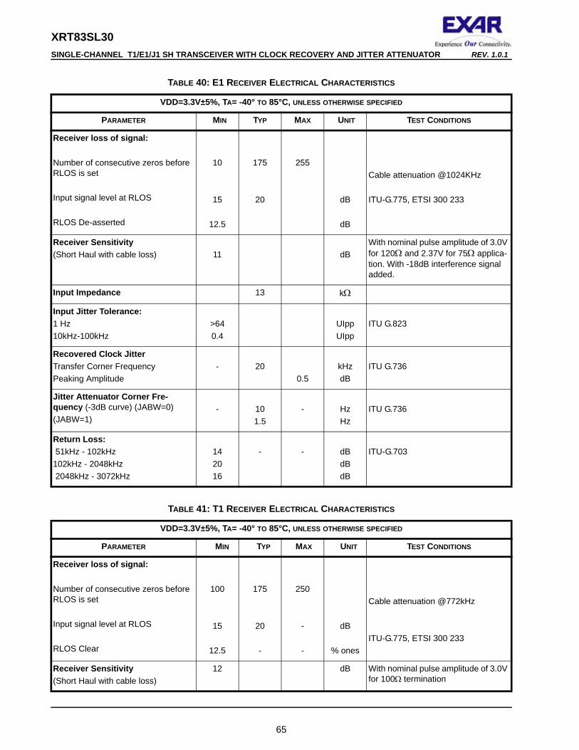
XRT83SL30 SINGLE-CHANNEL T1/E1/J1 SH TRANSCEIVER WITH CLOCK RECOVERY AND JITTER ATTENUATOR REV. 1.0.1
TABLE 40: E1 RECEIVER ELECTRICAL CHARACTERISTICS
VDD=3.3V±5%, TA= -40° TO 85°C, UNLESS OTHERWISE SPECIFIED
PARAMETER MIN TYP MAX UNIT TEST CONDITIONS
Receiver loss of signal:
Number of consecutive zeros before RLOS is set
Input signal level at RLOS
RLOS De-asserted
10
15
12.5
175
20
255
dB
dB
Cable attenuation @1024KHz
ITU-G.775, ETSI 300 233
Receiver Sensitivity (Short Haul with cable loss) 11 dB
With nominal pulse amplitude of 3.0V for 120Ω and 2.37V for 75Ω applica-tion. With -18dB interference signal added.
Input Impedance 13 kΩ
Input Jitter Tolerance: 1 Hz10kHz-100kHz
>640.4
UIppUIpp
ITU G.823
Recovered Clock Jitter Transfer Corner Frequency Peaking Amplitude
- 200.5
kHz dB
ITU G.736
Jitter Attenuator Corner Fre-quency (-3dB curve) (JABW=0)(JABW=1)
- 101.5
- HzHz
ITU G.736
Return Loss: 51kHz - 102kHz 102kHz - 2048kHz 2048kHz - 3072kHz
142016
- - dBdBdB
ITU-G.703
TABLE 41: T1 RECEIVER ELECTRICAL CHARACTERISTICS
VDD=3.3V±5%, TA= -40° TO 85°C, UNLESS OTHERWISE SPECIFIED
PARAMETER MIN TYP MAX UNIT TEST CONDITIONS
Receiver loss of signal:
Number of consecutive zeros before RLOS is set
Input signal level at RLOS
RLOS Clear
100
15
12.5
175
20
-
250
-
-
dB
% ones
Cable attenuation @772kHz
ITU-G.775, ETSI 300 233
Receiver Sensitivity(Short Haul with cable loss)
12 dB With nominal pulse amplitude of 3.0V for 100Ω termination
65
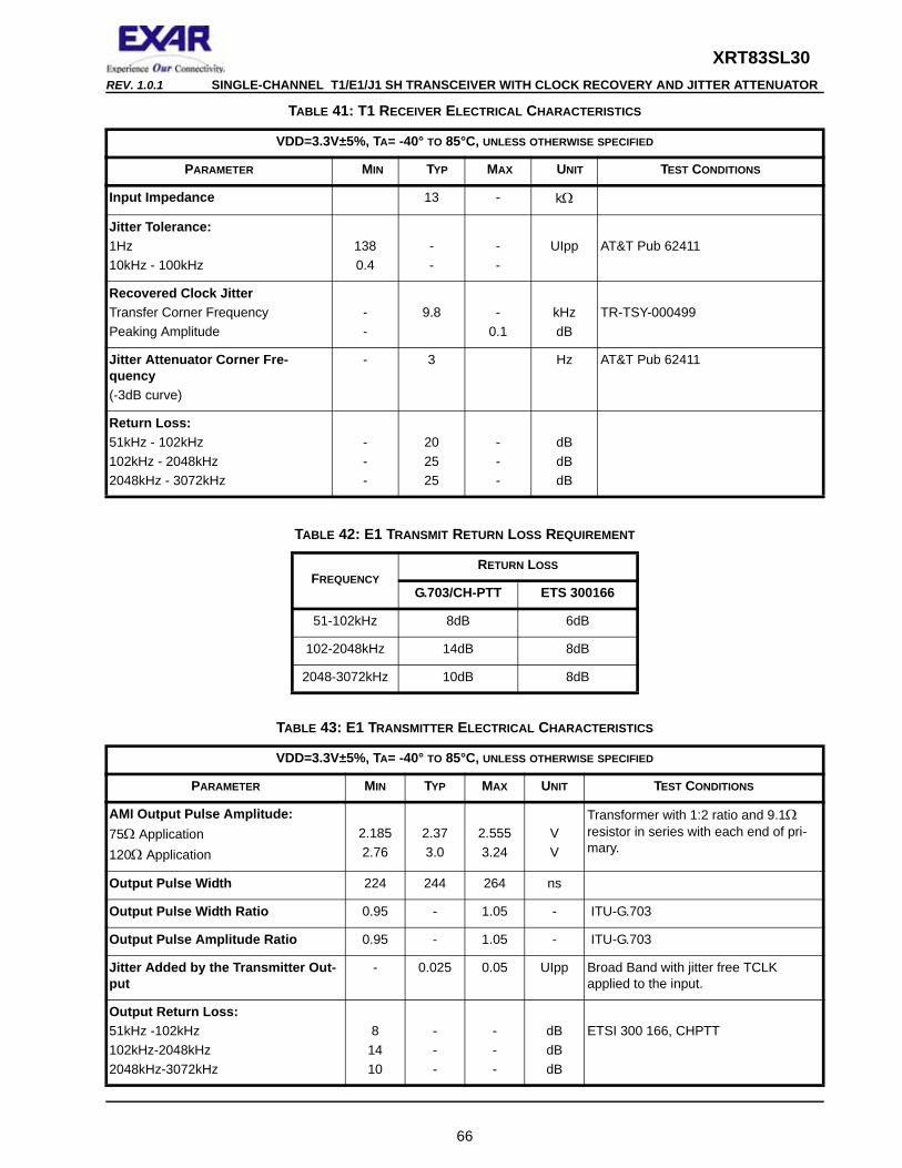
XRT83SL30REV. 1.0.1 SINGLE-CHANNEL T1/E1/J1 SH TRANSCEIVER WITH CLOCK RECOVERY AND JITTER ATTENUATOR
Input Impedance 13 - kΩ
Jitter Tolerance:1Hz10kHz - 100kHz
1380.4
--
--
UIpp AT&T Pub 62411
Recovered Clock JitterTransfer Corner FrequencyPeaking Amplitude
--
9.8 -0.1
kHzdB
TR-TSY-000499
Jitter Attenuator Corner Fre-quency(-3dB curve)
- 3 Hz AT&T Pub 62411
Return Loss:51kHz - 102kHz102kHz - 2048kHz2048kHz - 3072kHz
---
202525
---
dBdBdB
TABLE 42: E1 TRANSMIT RETURN LOSS REQUIREMENT
FREQUENCYRETURN LOSS
G.703/CH-PTT ETS 300166
51-102kHz 8dB 6dB
102-2048kHz 14dB 8dB
2048-3072kHz 10dB 8dB
TABLE 43: E1 TRANSMITTER ELECTRICAL CHARACTERISTICS
VDD=3.3V±5%, TA= -40° TO 85°C, UNLESS OTHERWISE SPECIFIED
PARAMETER MIN TYP MAX UNIT TEST CONDITIONS
AMI Output Pulse Amplitude:75Ω Application120Ω Application
2.1852.76
2.373.0
2.5553.24
VV
Transformer with 1:2 ratio and 9.1Ω resistor in series with each end of pri-mary.
Output Pulse Width 224 244 264 ns
Output Pulse Width Ratio 0.95 - 1.05 - ITU-G.703
Output Pulse Amplitude Ratio 0.95 - 1.05 - ITU-G.703
Jitter Added by the Transmitter Out-put
- 0.025 0.05 UIpp Broad Band with jitter free TCLK applied to the input.
Output Return Loss:51kHz -102kHz102kHz-2048kHz2048kHz-3072kHz
81410
---
---
dBdBdB
ETSI 300 166, CHPTT
TABLE 41: T1 RECEIVER ELECTRICAL CHARACTERISTICS
VDD=3.3V±5%, TA= -40° TO 85°C, UNLESS OTHERWISE SPECIFIED
PARAMETER MIN TYP MAX UNIT TEST CONDITIONS
66
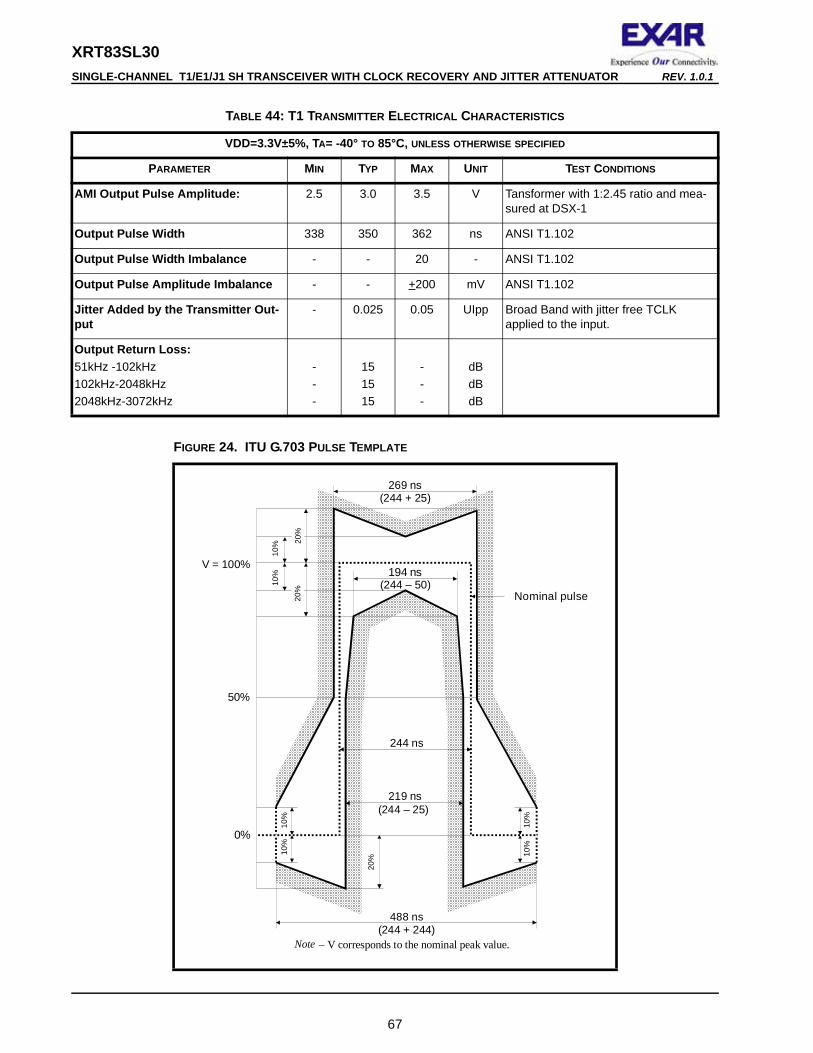
XRT83SL30 SINGLE-CHANNEL T1/E1/J1 SH TRANSCEIVER WITH CLOCK RECOVERY AND JITTER ATTENUATOR REV. 1.0.1
TABLE 44: T1 TRANSMITTER ELECTRICAL CHARACTERISTICS
VDD=3.3V±5%, TA= -40° TO 85°C, UNLESS OTHERWISE SPECIFIED
PARAMETER MIN TYP MAX UNIT TEST CONDITIONS
AMI Output Pulse Amplitude: 2.5 3.0 3.5 V Tansformer with 1:2.45 ratio and mea-sured at DSX-1
Output Pulse Width 338 350 362 ns ANSI T1.102
Output Pulse Width Imbalance - - 20 - ANSI T1.102
Output Pulse Amplitude Imbalance - - +200 mV ANSI T1.102
Jitter Added by the Transmitter Out-put
- 0.025 0.05 UIpp Broad Band with jitter free TCLK applied to the input.
Output Return Loss:51kHz -102kHz102kHz-2048kHz2048kHz-3072kHz
---
151515
---
dBdBdB
FIGURE 24. ITU G.703 PULSE TEMPLATE
10%
10%
10%
10%
10%
10%
269 ns(244 + 25)
194 ns(244 – 50)
244 ns
219 ns(244 – 25)
488 ns(244 + 244)
0%
50%
20%
V = 100%
Nominal pulse
Note – V corresponds to the nominal peak value.
20%
20%
67
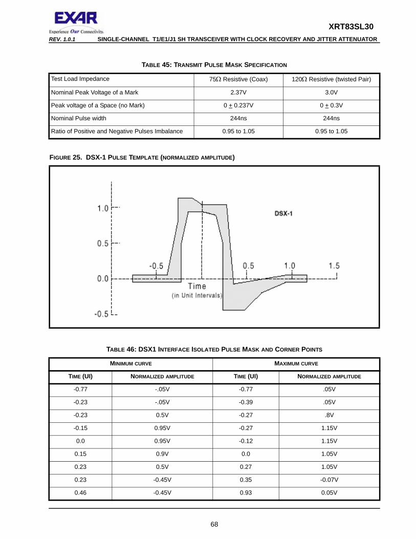
XRT83SL30REV. 1.0.1 SINGLE-CHANNEL T1/E1/J1 SH TRANSCEIVER WITH CLOCK RECOVERY AND JITTER ATTENUATOR
TABLE 45: TRANSMIT PULSE MASK SPECIFICATION
Test Load Impedance 75Ω Resistive (Coax) 120Ω Resistive (twisted Pair)
Nominal Peak Voltage of a Mark 2.37V 3.0V
Peak voltage of a Space (no Mark) 0 + 0.237V 0 + 0.3V
Nominal Pulse width 244ns 244ns
Ratio of Positive and Negative Pulses Imbalance 0.95 to 1.05 0.95 to 1.05
FIGURE 25. DSX-1 PULSE TEMPLATE (NORMALIZED AMPLITUDE)
TABLE 46: DSX1 INTERFACE ISOLATED PULSE MASK AND CORNER POINTS
MINIMUM CURVE MAXIMUM CURVE
TIME (UI) NORMALIZED AMPLITUDE TIME (UI) NORMALIZED AMPLITUDE
-0.77 -.05V -0.77 .05V
-0.23 -.05V -0.39 .05V
-0.23 0.5V -0.27 .8V
-0.15 0.95V -0.27 1.15V
0.0 0.95V -0.12 1.15V
0.15 0.9V 0.0 1.05V
0.23 0.5V 0.27 1.05V
0.23 -0.45V 0.35 -0.07V
0.46 -0.45V 0.93 0.05V
68
XRT83SL30 SINGLE-CHANNEL T1/E1/J1 SH TRANSCEIVER WITH CLOCK RECOVERY AND JITTER ATTENUATOR REV. 1.0.1
0.66 -0.2V 1.16 0.05V
0.93 -0.05V
1.16 -0.05V
TABLE 47: AC ELECTRICAL CHARACTERISTICS
(TA=25°C, VDD=3.3V±5%, UNLESS OTHERWISE SPECIFIED)
PARAMETER SYMBOL MIN TYP MAX UNITS
E1 MCLK Clock Frequency - 2.048 - MHz
T1 MCLK Clock Frequency - 1.544 - MHz
MCLK Clock Duty Cycle 40 - 60 %
MCLK Clock Tolerance - ±50 - ppm
TCLK Duty Cycle TCDU 30 50 70 %
Transmit Data Setup Time TSU 50 - - ns
Transmit Data Hold Time THO 30 - - ns
TCLK Rise Time(10%/90%) TCLKR - - 40 ns
TCLK Fall Time(90%/10%) TCLKF - - 40 ns
RCLK Duty Cycle RCDU 45 50 55 %
Receive Data Setup Time RSU 150 - - ns
Receive Data Hold Time RHO 150 - - ns
RCLK to Data Delay RDY - - 40 ns
RCLK Rise Time(10%/90%) with 25pF Loading.
RCLKR - - 40 ns
RCLK Fall Time(90%/10%) with 25pF Loading.
RCLKF 40 ns
TABLE 46: DSX1 INTERFACE ISOLATED PULSE MASK AND CORNER POINTS
MINIMUM CURVE MAXIMUM CURVE
TIME (UI) NORMALIZED AMPLITUDE TIME (UI) NORMALIZED AMPLITUDE
69
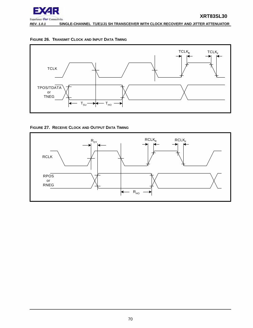
XRT83SL30REV. 1.0.1 SINGLE-CHANNEL T1/E1/J1 SH TRANSCEIVER WITH CLOCK RECOVERY AND JITTER ATTENUATOR
FIGURE 26. TRANSMIT CLOCK AND INPUT DATA TIMING
FIGURE 27. RECEIVE CLOCK AND OUTPUT DATA TIMING
TCLKR TCLKF
TCLK
TPOS/TDATAor
TNEG
TSU THO
RCLKR RCLKF
RCLK
RPOSor
RNEG
RDY
RHO
70
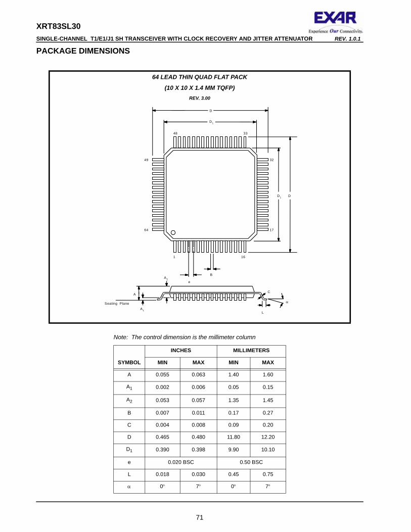
XRT83SL30 SINGLE-CHANNEL T1/E1/J1 SH TRANSCEIVER WITH CLOCK RECOVERY AND JITTER ATTENUATOR REV. 1.0.1
PACKAGE DIMENSIONS
64 LEAD THIN QUAD FLAT PACK
(10 X 10 X 1.4 MM TQFP)REV. 3.00
Note: The control dimension is the millimeter column
INCHES MILLIMETERS
SYMBOL MIN MAX MIN MAX
A 0.055 0.063 1.40 1.60
A1 0.002 0.006 0.05 0.15
A2 0.053 0.057 1.35 1.45
B 0.007 0.011 0.17 0.27
C 0.004 0.008 0.09 0.20
D 0.465 0.480 11.80 12.20
D1 0.390 0.398 9.90 10.10
e 0.020 BSC 0.50 BSC
L 0.018 0.030 0.45 0.75
α 0° 7° 0° 7°
48 33
32
17
1 16
49
64
D
D1
DD1
B
eA2
α
A1
A
Seating Plane
L
C
71
XRT83SL30REV. 1.0.1 SINGLE-CHANNEL T1/E1/J1 SH TRANSCEIVER WITH CLOCK RECOVERY AND JITTER ATTENUATOR
ORDERING INFORMATION
REVISION HISTORY
Rev. P1.0.0 Initial issue.
Rev. P1.0.1 Removed TERCNTL function (pin 46). Pins 61 and 62 are internally pulled Low. Set GIE bit to “0” to globally disable interrupt generation.Bit 7 of control register 2 and bit 1 of control register 3 are Reserved. Changed definition of Bits D6-D0 of tables 27 - 34. Removed references to long haul.
Rev. P1.0.3 Removed TERCNTL, TXTEST[[0:2], INSBPV from block diagram. Removed - Selectable receiver sensitivity from 0 to 36dB cable loss, and - High Receiver Interface Immunity, from Features section. Edit EQC[4:0] to be input only on block diagram. Corrected RXMUTE, TCLK, JABW, MCKLE1, CLKSEL [2:0], RXTSEL, TERSEL[1:0], RXRES[1:0], EQC4, ATAOS, NLCD in the pin descriptions section. Replaced the Functional Description section. Edits to Table 18: Microprocessor Register Bit Map, Table 21: Microprocessor Register #2 Bit Description, Table 35: Microprocessor Register #16 Bit Description
Rev P1.0.4 Table 35: Microprocessor Register #17 Bit Description, edit E1 clock MCLKRATE= “0” and T1/J1 clock MCLKRATE=”1” .
Rev 1.0.0 Final Release
Rev. 1.0.1 Corrected package dimensions in ordering information, page 3.
TABLE 48.
PART # PACKAGE OPERATING TEMPERATURE RANGE
XRT83SL30IV 64 Pin TQFP -40oC to +85oC
THERMAL INFORMATION Theta - JA = 38° C/W Theta JC = 7° C/W
72
XRT83SL30 SINGLE-CHANNEL T1/E1/J1 SH TRANSCEIVER WITH CLOCK RECOVERY AND JITTER ATTENUATOR REV. 1.0.1
73
NOTICE
EXAR Corporation reserves the right to make changes to the products contained in this publication in order to improve design, performance or reliability. EXAR Corporation assumes no responsibility for the use of any circuits described herein, conveys no license under any patent or other right, and makes no representation that the circuits are free of patent infringement. Charts and schedules contained here in are only for illustration purposes and may vary depending upon a user’s specific application. While the information in this publication has been carefully checked; no responsibility, however, is assumed for inaccuracies.
EXAR Corporation does not recommend the use of any of its products in life support applications where the failure or malfunction of the product can reasonably be expected to cause failure of the life support system or to significantly affect its safety or effectiveness. Products are not authorized for use in such applications unless EXAR Corporation receives, in writing, assurances to its satisfaction that: (a) the risk of injury or damage has been minimized; (b) the user assumes all such risks; (c) potential liability of EXAR Corporation is adequately protected under the circumstances.
Copyright 2006 EXAR Corporation
Datasheet June 2006.
Send your UART technical inquiry with technical details to hotline: [email protected].
Reproduction, in part or whole, without the prior written consent of EXAR Corporation is prohibited.


![Complex Data For single channel data [1] – Real and imag. images are normally distributed with N(S, σ 2 ) – Then magnitude images follow Rice dist., which.](https://static.fdocument.org/doc/165x107/5519d135550346695e8b4cc1/complex-data-for-single-channel-data-1-real-and-imag-images-are-normally-distributed-with-ns-2-then-magnitude-images-follow-rice-dist-which.jpg)