Xilinx Sine/Cosine Look-Up Table v5 · The core computes sin(Θ) and cos(Θ) and presents the...
9
DS275 April 28, 2005 www.xilinx.com 1 Product Specification © 2005 Xilinx, Inc. All rights reserved. XILINX, the Xilinx logo, and other designated brands included herein are trademarks of Xilinx, Inc. All other trademarks are the property of their respective owners. Xilinx is providing this design, code, or information "as is." By providing the design, code, or information as one possible implementation of this feature, application, or standard, Xilinx makes no representation that this implementation is free from any claims of infringement. You are responsible for obtaining any rights you may require for your implementation. Xilinx expressly disclaims any warranty whatsoever with respect to the adequacy of the implementation, including but not limited to any warranties or representations that this implementation is free from claims of infringement and any implied warranties of merchantability or fitness for a particular purpose. Features • Drop-in module for Virtex™, Virtex-E, and Virtex-II, Virtex-II Pro, Virtex-4, Spartan™-II, Spartan-IIE, Spartan-3, and Spartan-3E FPGAs • User specified option for table value storage in Distributed/Block Memory • Supports THETA input widths of 3 to 10 bits for Distributed ROM and 3 to 16 bits for Block ROM • Supports output Sine/Cosine widths of 4 to 32 bits • Supports negative Sine/Cosine outputs • Symmetric Output option uses an extra integer bit in the output so that the effective range is -1.0 to +1.0 • Automatically selects from quarter wave storage and 360° wave storage for optimum implementation • Variable pipelining option to improve overall clock rates • Incorporates Xilinx Smart-IP™ technology for utmost parameterization and optimum implementation • Uses relationally placed macro (RPM) mapping and placement technology, for maximum and predictable performance • To be used with Xilinx CORE Generator™ system 7.1i and later Functional Description The Sine/Cosine module accepts an unsigned input value THETA and produces two’s complement outputs of SINE (THETA) and/or COSINE (THETA). The user controls the input THETA width and output SINE and /or COSINE width values. Equation 1 defines the relationship between the integer input angle THETA supplied to the core (refer to Figure 1) and the actual radian angle Θ . The core computes sin(Θ) and cos(Θ ) and presents the two’s complement on the output ports SINE and COSINE respectively. Expressed as fractional fixed-point values, the output samples are in the inter- val (refer to equation 2) when the non-symmetrical out- put option is selected or (refer to equation 3) when the symmetrical output option is selected. The values for the sine and cosine wave are stored in an internal ROM. Depending on what the user specifies for the THETA input width and SINE and/or COSINE output width, either a full wave or quarter wave is stored in the ROM table. When only a quarter wave is stored, the full 360-degree output is generated using additional internal logic. The selection of quarter or full wave storage is performed automatically to produce the most efficient implementation. 0 Sine/Cosine Look-Up Table v5.0 DS275 April 28, 2005 0 0 Product Specification θ THETA 2 Π 2 THETA_WIDTH ----------------------------------- radians = Eq. 1 Eq. 2 2 OUTPUT_WIDTH 1 – – 2 OUTPUT_WIDTH 1 – ------------------------------------------------- +2 OUTPUT_WIDTH 1 – 1 – 2 OUTPUT_WIDTH 1 – ---------------------------------------------------------- , Eq. 3 2 OUTPUT_WIDTH 2 – – 2 OUTPUT_WIDTH 2 – ------------------------------------------------- +2 OUTPUT_WIDTH 2 – 1 – 2 OUTPUT_WIDTH 2 – ---------------------------------------------------------- , Discontinued IP
Transcript of Xilinx Sine/Cosine Look-Up Table v5 · The core computes sin(Θ) and cos(Θ) and presents the...
Features• Drop-in module for Virtex™, Virtex-E, and Virtex-II,
Virtex-II Pro, Virtex-4, Spartan™-II, Spartan-IIE, Spartan-3, and Spartan-3E FPGAs
• User specified option for table value storage in Distributed/Block Memory
• Supports THETA input widths of 3 to 10 bits for Distributed ROM and 3 to 16 bits for Block ROM
• Supports output Sine/Cosine widths of 4 to 32 bits
• Supports negative Sine/Cosine outputs
• Symmetric Output option uses an extra integer bit in the output so that the effective range is -1.0 to +1.0
• Automatically selects from quarter wave storage and 360° wave storage for optimum implementation
• Variable pipelining option to improve overall clock rates
• Incorporates Xilinx Smart-IP™ technology for utmost parameterization and optimum implementation
• Uses relationally placed macro (RPM) mapping and placement technology, for maximum and predictable performance
• To be used with Xilinx CORE Generator™ system 7.1i and later
Functional DescriptionThe Sine/Cosine module accepts an unsigned inputvalue THETA and produces two’s complement outputsof SINE (THETA) and/or COSINE (THETA). The usercontrols the input THETA width and output SINE and/or COSINE width values.
Equation 1 defines the relationship between the integerinput angle THETA supplied to the core (refer toFigure 1) and the actual radian angle Θ.
The core computes sin(Θ) and cos(Θ) and presents thetwo’s complement on the output ports SINE andCOSINE respectively. Expressed as fractionalfixed-point values, the output samples are in the inter-val (refer to equation 2) when the non-symmetrical out-put option is selected or (refer to equation 3) when thesymmetrical output option is selected.
The values for the sine and cosine wave are stored in aninternal ROM. Depending on what the user specifiesfor the THETA input width and SINE and/or COSINEoutput width, either a full wave or quarter wave isstored in the ROM table. When only a quarter wave isstored, the full 360-degree output is generated usingadditional internal logic. The selection of quarter or fullwave storage is performed automatically to producethe most efficient implementation.
0
Sine/Cosine Look-Up Tablev5.0
DS275 April 28, 2005 0 0 Product Specification
θ THETA 2Π2THETA_WIDTH------------------------------------radians= Eq. 1
Eq. 22OUTPUT_WIDTH 1––
2OUTPUT_WIDTH 1–------------------------------------------------- +2OUTPUT_WIDTH 1– 1–
2OUTPUT_WIDTH 1–-----------------------------------------------------------,
Eq. 32OUTPUT_WIDTH 2––
2OUTPUT_WIDTH 2–------------------------------------------------- +2OUTPUT_WIDTH 2– 1–
2OUTPUT_WIDTH 2–-----------------------------------------------------------,
Discontinued IP
DS275 April 28, 2005 www.xilinx.com 1Product Specification
© 2005 Xilinx, Inc. All rights reserved. XILINX, the Xilinx logo, and other designated brands included herein are trademarks of Xilinx, Inc. All other trademarks are the property of their respective owners. Xilinx is providing this design, code, or information "as is." By providing the design, code, or information as one possible implementation of this feature, application, or standard, Xilinx makes no representation that this implementation is free from any claims of infringement. You are responsible for obtaining any rights you may require for your implementation. Xilinx expressly disclaims any warranty whatsoever with respect to the adequacy of the implementation, including but not limited to any warranties or representations that this implementation is free from claims of infringement and any implied warranties of merchantability or fitness for a particular purpose.
Sine/Cosine Look-Up Table v5.0
2
D
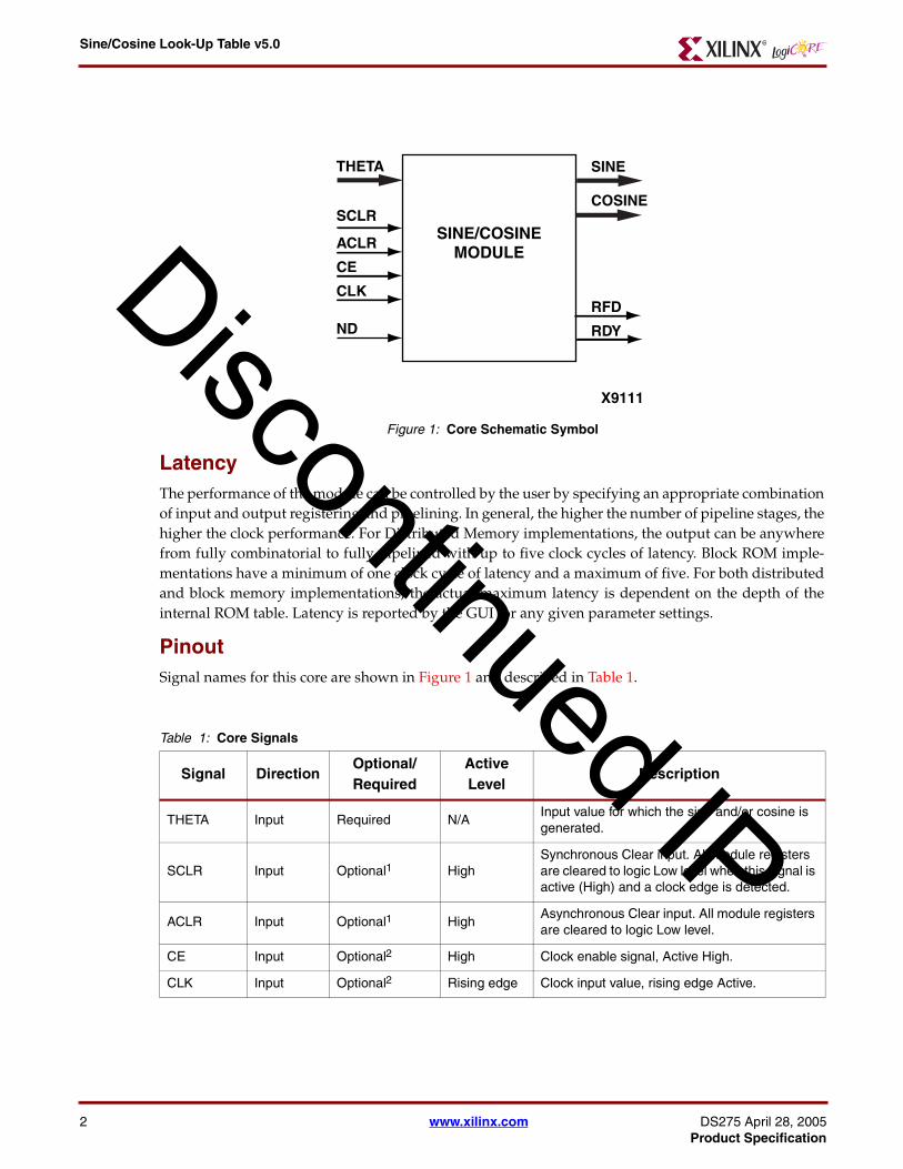
LatencyThe performance of the module can be controlled by the user by specifying an appropriate combinationof input and output registering and pipelining. In general, the higher the number of pipeline stages, thehigher the clock performance. For Distributed Memory implementations, the output can be anywherefrom fully combinatorial to fully pipelined with up to five clock cycles of latency. Block ROM imple-mentations have a minimum of one clock cycle of latency and a maximum of five. For both distributedand block memory implementations, the actual maximum latency is dependent on the depth of theinternal ROM table. Latency is reported by the GUI for any given parameter settings.PinoutSignal names for this core are shown in Figure 1 and described in Table 1.
Figure Top x-ref 1
Figure 1: Core Schematic Symbol
Table 1: Core Signals
Signal DirectionOptional/Required
ActiveLevel
Description
THETA Input Required N/AInput value for which the sine and/or cosine is generated.
SCLR Input Optional1 HighSynchronous Clear input. All module registers are cleared to logic Low level when this signal is active (High) and a clock edge is detected.
ACLR Input Optional1 HighAsynchronous Clear input. All module registers are cleared to logic Low level.
CE Input Optional2 High Clock enable signal, Active High.
CLK Input Optional2 Rising edge Clock input value, rising edge Active.
THETA
SCLR
ACLR
CE
CLK
ND
SINE
COSINE
SINE/COSINEMODULE
RFD
RDY
X9111
iscontinued IP
www.xilinx.com DS275 April 28, 2005Product Specification
Sine/Cosine Look-Up Table v5.0
DS275 ApriProduct Sp
D
ND Input Optional4 HighNew Data input signal. Indicates to the module that a new THETA value is being input on the THETA input port. Assertion of ND initiates the generation of the Sine and/or the Cosine output value.
SINE Output Optional3 N/A Sine value output for the THETA input value.
COSINE Output Optional3 N/A Cosine value output for the THETA input value.
RFD Output Optional4 HighReady For Data output signal indicates that the module can accept new THETA input values.
RDY Output Optional4 HighReady output signal indicates that a valid Sine and/or Cosine value is available on the output ports.
Notes:
1. Clear options are available only when the output is registered.
2. A CLK signal is required when Block ROM implementation is specified, or when input or output registering is requested.
3. Either the Sine, Cosine, or both outputs must be specified.
4. ND, RFD, and RDY are signals which are activated as a group when the Handshaking Options setting is enabled.
Table 1: Core Signals
Signal DirectionOptional/Required
ActiveLevel
Description
iscontinued IP
l 28, 2005 www.xilinx.com 3ecification
Sine/Cosine Look-Up Table v5.0
4
D
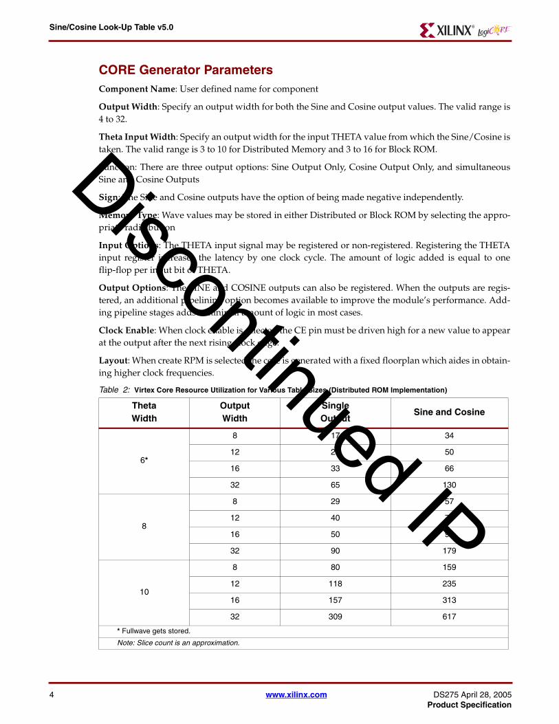
CORE Generator ParametersComponent Name: User defined name for componentOutput Width: Specify an output width for both the Sine and Cosine output values. The valid range is4 to 32.
Theta Input Width: Specify an output width for the input THETA value from which the Sine/Cosine istaken. The valid range is 3 to 10 for Distributed Memory and 3 to 16 for Block ROM.
Function: There are three output options: Sine Output Only, Cosine Output Only, and simultaneousSine and Cosine Outputs
Sign: The Sine and Cosine outputs have the option of being made negative independently.
Memory Type: Wave values may be stored in either Distributed or Block ROM by selecting the appro-priate radio button
Input Options: The THETA input signal may be registered or non-registered. Registering the THETAinput register increases the latency by one clock cycle. The amount of logic added is equal to oneflip-flop per input bit of THETA.
Output Options: The SINE and COSINE outputs can also be registered. When the outputs are regis-tered, an additional pipelining option becomes available to improve the module’s performance. Add-ing pipeline stages adds a minimal amount of logic in most cases.
Clock Enable: When clock enable is selected the CE pin must be driven high for a new value to appearat the output after the next rising clock edge.
Layout: When create RPM is selected the core is generated with a fixed floorplan which aides in obtain-ing higher clock frequencies.
Table 2: Virtex Core Resource Utilization for Various Table Sizes (Distributed ROM Implementation)
ThetaWidth
OutputWidth
Single Output
Sine and Cosine
6*
8 17 34
12 25 50
16 33 66
32 65 130
8
8 29 57
12 40 79
16 50 99
32 90 179
10
8 80 159
12 118 235
16 157 313
32 309 617
* Fullwave gets stored.
Note: Slice count is an approximation.
iscontinued IP
www.xilinx.com DS275 April 28, 2005Product Specification
Sine/Cosine Look-Up Table v5.0
DS275 ApriProduct Sp
D
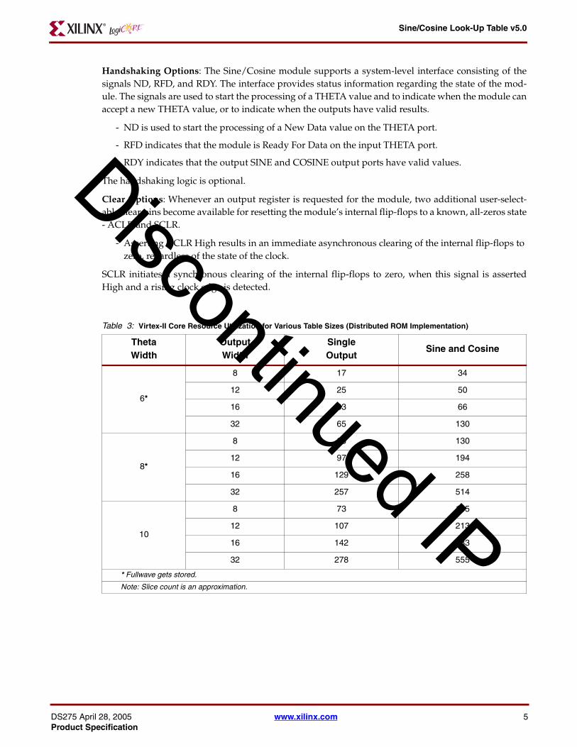
Handshaking Options: The Sine/Cosine module supports a system-level interface consisting of thesignals ND, RFD, and RDY. The interface provides status information regarding the state of the mod-ule. The signals are used to start the processing of a THETA value and to indicate when the module canaccept a new THETA value, or to indicate when the outputs have valid results.- ND is used to start the processing of a New Data value on the THETA port.
- RFD indicates that the module is Ready For Data on the input THETA port.
- RDY indicates that the output SINE and COSINE output ports have valid values.
The handshaking logic is optional.
Clear Options: Whenever an output register is requested for the module, two additional user-select-able clear pins become available for resetting the module’s internal flip-flops to a known, all-zeros state- ACLR and SCLR.
- Asserting ACLR High results in an immediate asynchronous clearing of the internal flip-flops to zero, regardless of the state of the clock.
SCLR initiates a synchronous clearing of the internal flip-flops to zero, when this signal is assertedHigh and a rising clock edge is detected.
Table 3: Virtex-II Core Resource Utilization for Various Table Sizes (Distributed ROM Implementation)
ThetaWidth
OutputWidth
Single Output
Sine and Cosine
6*
8 17 34
12 25 50
16 33 66
32 65 130
8*
8 65 130
12 97 194
16 129 258
32 257 514
10
8 73 145
12 107 213
16 142 283
32 278 555
* Fullwave gets stored.
Note: Slice count is an approximation.
iscontinued IP
l 28, 2005 www.xilinx.com 5ecification
Sine/Cosine Look-Up Table v5.0
6
D
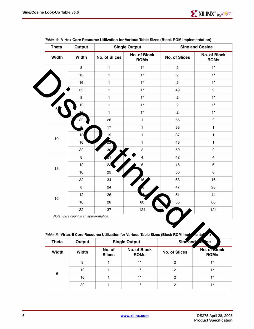
Table 4: Virtex Core Resource Utilization for Various Table Sizes (Block ROM Implementation)Theta Output Single Output Sine and Cosine
Width Width No. of SlicesNo. of Block
ROMsNo. of Slices
No. of Block ROMs
6
8 1 1* 2 1*
12 1 1* 2 1*
16 1 1* 2 1*
32 1 1* 49 2
8
8 1 1* 2 1*
12 1 1* 2 1*
16 1 1* 2 1*
32 28 1 55 2
10
8 17 1 33 1
12 19 1 37 1
16 22 1 43 1
32 30 2 59 2
13
8 21 4 42 4
12 23 6 46 6
16 25 8 50 8
32 34 16 68 16
16
8 24 28 47 28
12 26 44 51 44
16 28 60 55 60
32 37 124 73 124
Note: Slice count is an approximation.
Table 5: Virtex-II Core Resource Utilization for Various Table Sizes (Block ROM Implementation)
Theta Output Single Output Sine and Cosine
Width WidthNo. of Slices
No. of Block ROMs
No. of SlicesNo. of Block
ROMs
6
8 1 1* 2 1*
12 1 1* 2 1*
16 1 1* 2 1*
32 1 1* 2 1*
iscontinued IP
www.xilinx.com DS275 April 28, 2005Product Specification
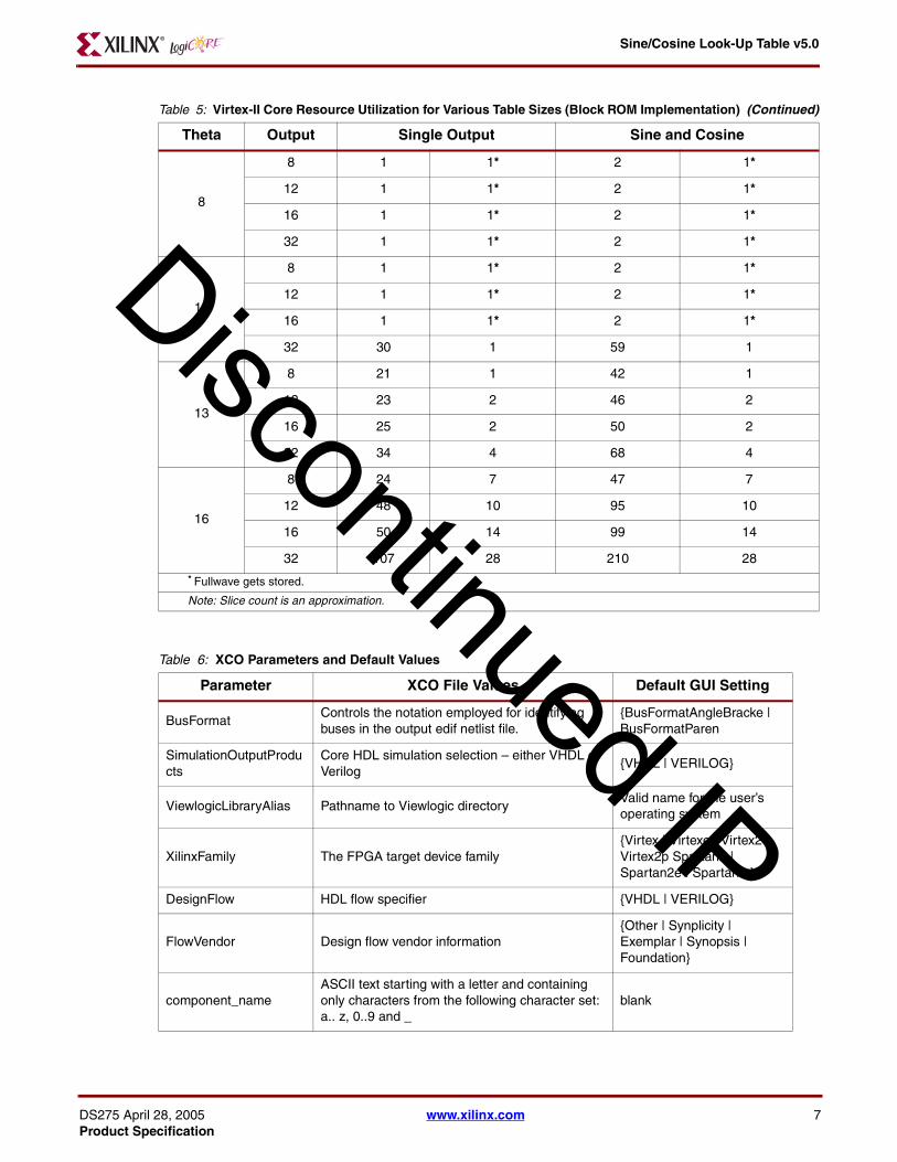
Sine/Cosine Look-Up Table v5.0
DS275 ApriProduct Sp
D
88 1 1* 2 1*
12 1 1* 2 1*
16 1 1* 2 1*
32 1 1* 2 1*
10
8 1 1* 2 1*
12 1 1* 2 1*
16 1 1* 2 1*
32 30 1 59 1
13
8 21 1 42 1
12 23 2 46 2
16 25 2 50 2
32 34 4 68 4
16
8 24 7 47 7
12 48 10 95 10
16 50 14 99 14
32 107 28 210 28* Fullwave gets stored.
Note: Slice count is an approximation.
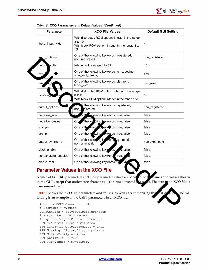
Table 6: XCO Parameters and Default Values
Parameter XCO File Values Default GUI Setting
BusFormatControls the notation employed for identifying buses in the output edif netlist file.
{BusFormatAngleBracke | BusFormatParen
SimulationOutputProducts
Core HDL simulation selection – either VHDL or Verilog
{VHDL | VERILOG}
ViewlogicLibraryAlias Pathname to Viewlogic directoryValid name for the user’s operating system
XilinxFamily The FPGA target device family{Virtex | Virtexe | Virtex2 | Virtex2p Spartan2 | Spartan2e | Spartan3 }
DesignFlow HDL flow specifier {VHDL | VERILOG}
FlowVendor Design flow vendor information{Other | Synplicity | Exemplar | Synopsis | Foundation}
component_nameASCII text starting with a letter and containing only characters from the following character set: a.. z, 0..9 and _
blank
Table 5: Virtex-II Core Resource Utilization for Various Table Sizes (Block ROM Implementation) (Continued)
Theta Output Single Output Sine and Cosine
iscontinued IP
l 28, 2005 www.xilinx.com 7ecification
Sine/Cosine Look-Up Table v5.0
8
D
Parameter Values in the XCO FileNames of XCO file parameters and their parameter values are identical to the names and values shownin the GUI, except that underscore characters (_) are used instead of spaces. The text in an XCO file iscase insensitive.
Table 2 shows the XCO file parameters and values, as well as summarizing the GUI defaults. The fol-lowing is an example of the CSET parameters in an XCO file:
# Xilinx CORE Generator 5.1i# Username = nyquistCOREGenPath = c:\visualcafe\projects# ProjectPath = H:\newcore# ExpandedProjectPath = H:\newcoreSET BusFormat = BusFormatParenSET SimulationOutputProducts = VHDLSET ViewlogicLibraryAlias = primarySET XilinxFamily = VirtexSET DesignFlow = VHDLSET FlowVendor = Synplicity
theta_input_width
With distributed ROM option: integer in the range 3 to 10.With block ROM option: integer in the range 3 to 16
4
input_optionsOne of the following keywords: registered, non_registered
non_registered
output_width Integer in the range 4 to 32 16
functionOne of the following keywords: sine, cosine, sine_and_cosine,
sine
memory_typeOne of the following keywords: dist_rom, block_rom
dist_rom
pipeline_stagesWith distributed ROM option: integer in the range 0 to 3With block ROM option: integer in the range 1 to 2
0
output_optionsOne of the following keywords: registered, non_registered
non_registered
negative_sine One of the following keywords: true, false false
negative_cosine One of the following keywords: true, false false
sclr_pin One of the following keywords: true, false false
aclr_pin One of the following keywords: true, false false
output_symmetryOne of the following keywords: symmetric, non-symmetric
non-symmetric
clock_enable One of the following keywords: true, false false
handshaking_enabled One of the following keywords: true, false false
create_rpm One of the following keywords: true, false false
Table 6: XCO Parameters and Default Values (Continued)
Parameter XCO File Values Default GUI Setting
iscontinued IP
www.xilinx.com DS275 April 28, 2005Product Specification
Sine/Cosine Look-Up Table v5.0
DS275 ApriProduct Sp
D
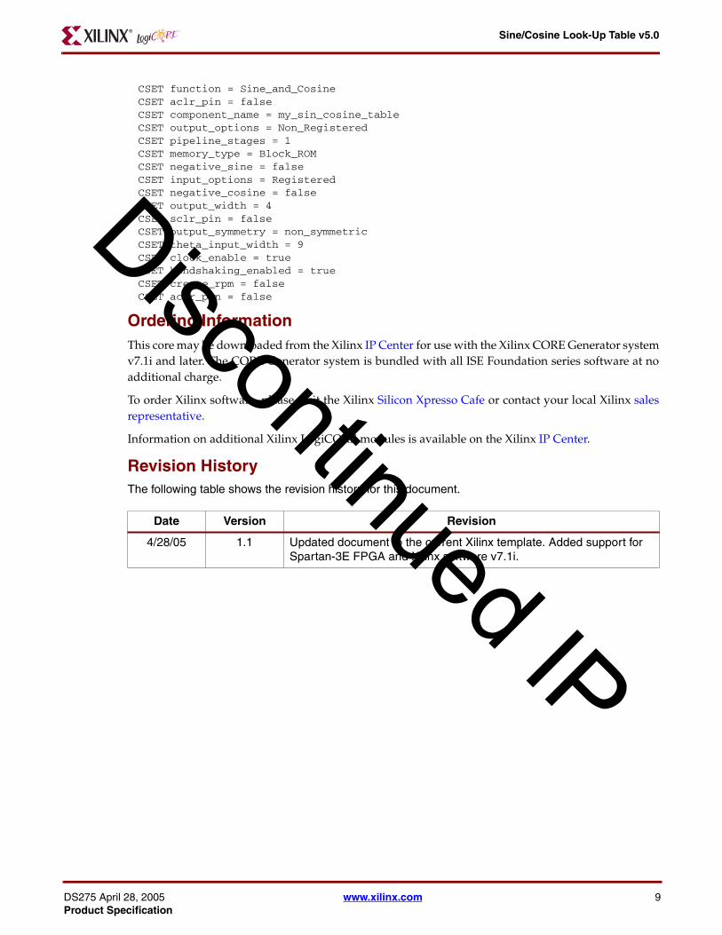
CSET function = Sine_and_CosineCSET aclr_pin = falseCSET component_name = my_sin_cosine_tableCSET output_options = Non_RegisteredCSET pipeline_stages = 1CSET memory_type = Block_ROMCSET negative_sine = falseCSET input_options = RegisteredCSET negative_cosine = falseCSET output_width = 4CSET sclr_pin = falseCSET output_symmetry = non_symmetricCSET theta_input_width = 9CSET clock_enable = trueCSET handshaking_enabled = trueCSET create_rpm = falseCSET aclr_pin = falseOrdering InformationThis core may be downloaded from the Xilinx IP Center for use with the Xilinx CORE Generator systemv7.1i and later. The CORE Generator system is bundled with all ISE Foundation series software at noadditional charge.
To order Xilinx software, please visit the Xilinx Silicon Xpresso Cafe or contact your local Xilinx salesrepresentative.
Information on additional Xilinx LogiCORE modules is available on the Xilinx IP Center.
Revision HistoryThe following table shows the revision history for this document.
Date Version Revision
4/28/05 1.1 Updated document to the current Xilinx template. Added support for Spartan-3E FPGA and Xilinx software v7.1i.
iscontinued IP
l 28, 2005 www.xilinx.com 9ecification