XC6120 E - Your analog power IC and the best power ... · 2/15 . XC6120 Series BLOCK DIAGRAMS (1)...
15
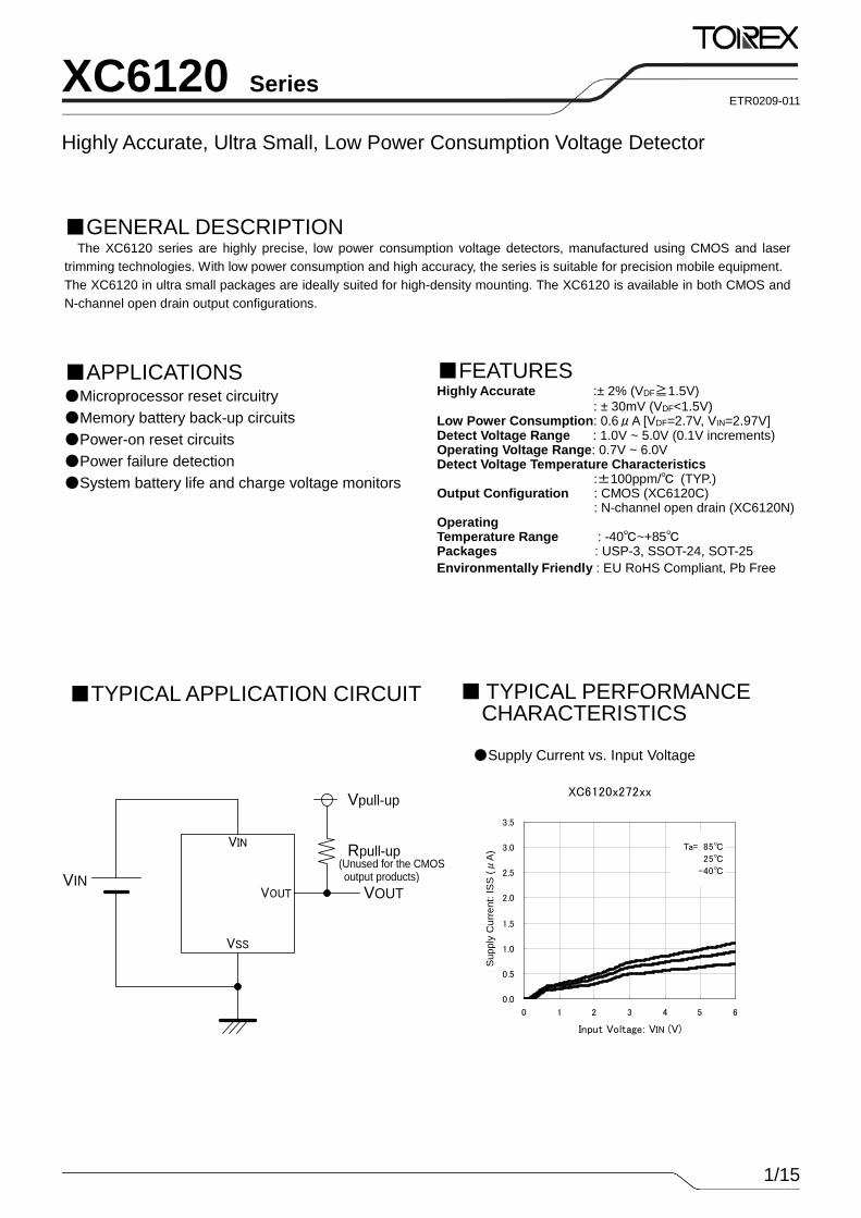
1/15 XC6120 Series Highly Accurate, Ultra Small, Low Power Consumption Voltage Detector XC6120x272xx 0.0 0.5 1.0 1.5 2.0 2.5 3.0 3.5 0 1 2 3 4 5 6 Input Voltage: VIN (V) Ta= 85℃ 25℃ -40℃ VIN VSS VOUT VIN VOUT Vpull-up Rpull-up ■GENERAL DESCRIPTION The XC6120 series are highly precise, low power consumption voltage detectors, manufactured using CMOS and laser trimming technologies. With low power consumption and high accuracy, the series is suitable for precision mobile equipment. The XC6120 in ultra small packages are ideally suited for high-density mounting. The XC6120 is available in both CMOS and N-channel open drain output configurations. ■APPLICATIONS ●Microprocessor reset circuitry ●Memory battery back-up circuits ●Power-on reset circuits ●Power failure detection ●System battery life and charge voltage monitors ■TYPICAL APPLICATION CIRCUIT ■ TYPICAL PERFORMANCE CHARACTERISTICS ●Supply Current vs. Input Voltage ETR0209-011 ■FEATURES Highly Accurate :± 2% (VDF≧1.5V) : ± 30mV (VDF<1.5V) Low Power Consumption: 0.6μA [VDF=2.7V, VIN=2.97V] Detect Voltage Range : 1.0V ~ 5.0V (0.1V increments) Operating Voltage Range: 0.7V ~ 6.0V Detect Voltage Temperature Characteristics :±100ppm/℃ (TYP.) Output Configuration : CMOS (XC6120C) : N-channel open drain (XC6120N) Operating Temperature Range : -40℃~+85℃ Packages : USP-3, SSOT-24, SOT-25 Environmentally Friendly : EU RoHS Compliant, Pb Free Supply Current: ISS (μA) (Unused for the CMOS output products)
Transcript of XC6120 E - Your analog power IC and the best power ... · 2/15 . XC6120 Series BLOCK DIAGRAMS (1)...
1/15
XC6120 Series Highly Accurate, Ultra Small, Low Power Consumption Voltage Detector
XC6120x272xx
0.0
0.5
1.0
1.5
2.0
2.5
3.0
3.5
0 1 2 3 4 5 6
Input Voltage: VIN (V)
Supp
ly C
urr
ent:
IS
S (
μA
) Ta= 85℃
25℃
-40℃
VIN
VSS
VOUTVIN
VOUT
Vpull-up
Rpull-up
■GENERAL DESCRIPTION The XC6120 series are highly precise, low power consumption voltage detectors, manufactured using CMOS and laser
trimming technologies. With low power consumption and high accuracy, the series is suitable for precision mobile equipment. The XC6120 in ultra small packages are ideally suited for high-density mounting. The XC6120 is available in both CMOS and N-channel open drain output configurations.
■APPLICATIONS ●Microprocessor reset circuitry ●Memory battery back-up circuits ●Power-on reset circuits ●Power failure detection ●System battery life and charge voltage monitors
■TYPICAL APPLICATION CIRCUIT ■ TYPICAL PERFORMANCE CHARACTERISTICS
●Supply Current vs. Input Voltage
ETR0209-011
■FEATURES Highly Accurate :± 2% (VDF≧1.5V) : ± 30mV (VDF<1.5V) Low Power Consumption: 0.6μA [VDF=2.7V, VIN=2.97V] Detect Voltage Range : 1.0V ~ 5.0V (0.1V increments) Operating Voltage Range: 0.7V ~ 6.0V Detect Voltage Temperature Characteristics :±100ppm/℃ (TYP.) Output Configuration : CMOS (XC6120C) : N-channel open drain (XC6120N) Operating Temperature Range : -40℃~+85℃ Packages : USP-3, SSOT-24, SOT-25 Environmentally Friendly : EU RoHS Compliant, Pb Free
Sup
ply
Cur
rent
: IS
S (μ
A)
(Unused for the CMOS output products)
2/15
XC6120 Series
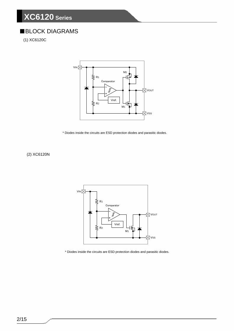
■BLOCK DIAGRAMS (1) XC6120C
(2) XC6120N
VOUT
VIN
R1
R2
M2
M1
VSS
Vref.
Comparator
VIN
VOUT
R1
R2M1
VSS
Vref.
Comparator
* Diodes inside the circuits are ESD protection diodes and parasitic diodes.
* Diodes inside the circuits are ESD protection diodes and parasitic diodes.
3/15
XC6120 Series
1 32
5 4
VINVOUT VSS
SOT-25(TOP VIEW)
NC NC
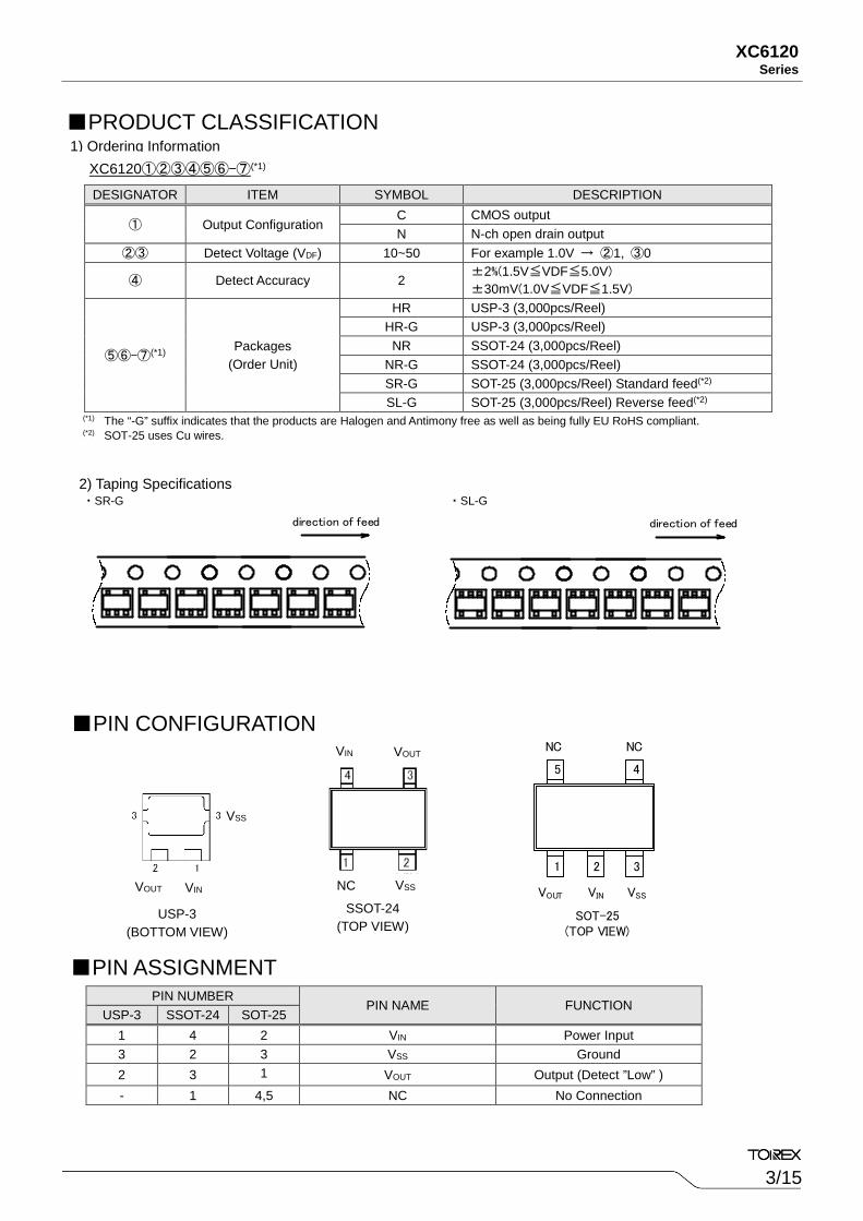
DESIGNATOR ITEM SYMBOL DESCRIPTION
① Output Configuration C CMOS output N N-ch open drain output
②③ Detect Voltage (VDF) 10~50 For example 1.0V → ②1, ③0
④ Detect Accuracy 2 ±2%(1.5V≦VDF≦5.0V)
±30mV(1.0V≦VDF≦1.5V)
⑤⑥-⑦(*1) Packages
(Order Unit)
HR USP-3 (3,000pcs/Reel) HR-G USP-3 (3,000pcs/Reel)
NR SSOT-24 (3,000pcs/Reel) NR-G SSOT-24 (3,000pcs/Reel) SR-G SOT-25 (3,000pcs/Reel) Standard feed(*2) SL-G SOT-25 (3,000pcs/Reel) Reverse feed(*2)
PIN NUMBER PIN NAME FUNCTION
USP-3 SSOT-24 SOT-25 1 4 2 VIN Power Input 3 2 3 VSS Ground 2 3 1 VOUT Output (Detect ”Low” ) - 1 4,5 NC No Connection
■PRODUCT CLASSIFICATION 1) Ordering Information
XC6120①②③④⑤⑥-⑦(*1)
(*1) The “-G” suffix indicates that the products are Halogen and Antimony free as well as being fully EU RoHS compliant. (*2) SOT-25 uses Cu wires.
2) Taping Specifications ・SR-G ・SL-G
direction of feed direction of feed
■PIN CONFIGURATION
■PIN ASSIGNMENT
SSOT-24 (TOP VIEW)
USP-3 (BOTTOM VIEW)
VSS
VIN VOUT VSS NC
VIN VOUT
4/15
XC6120 Series
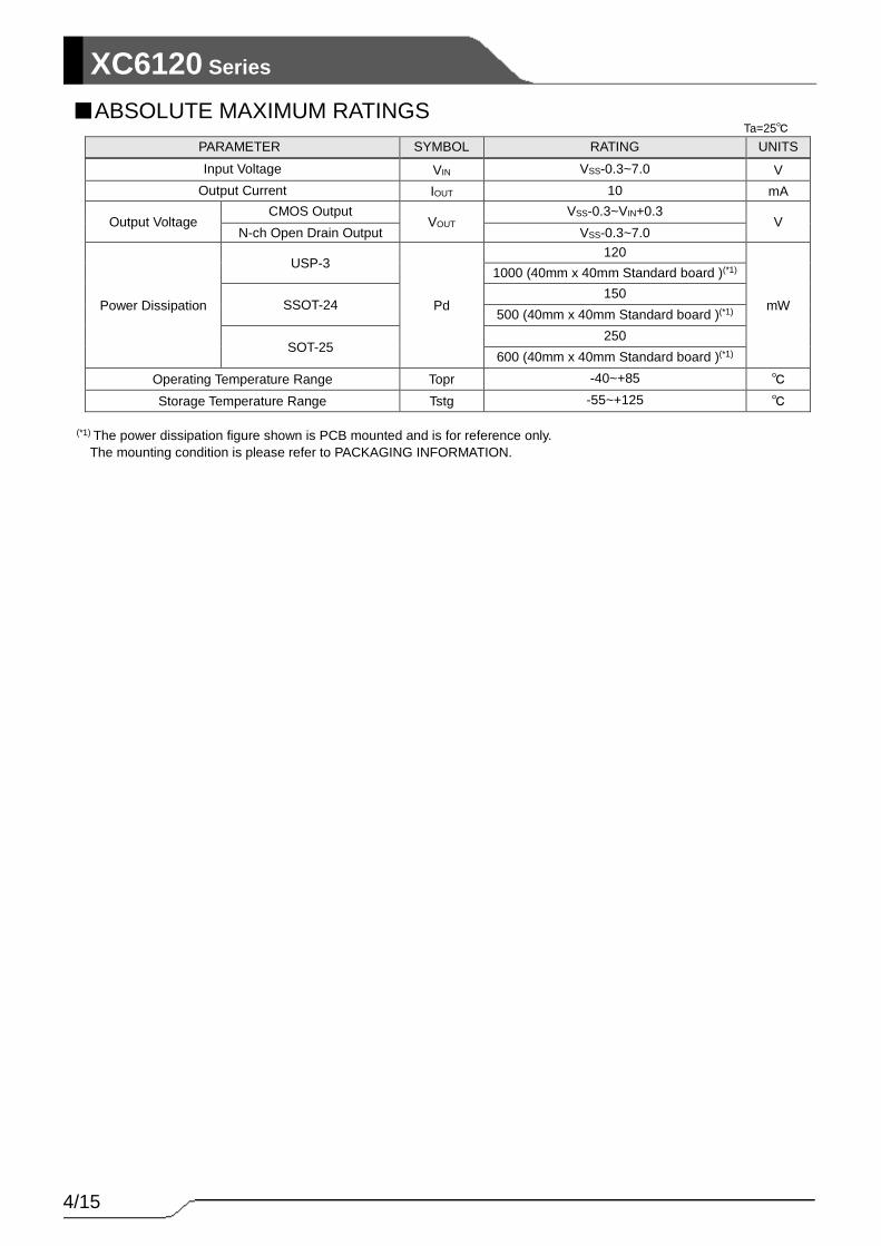
(*1) The power dissipation figure shown is PCB mounted and is for reference only. The mounting condition is please refer to PACKAGING INFORMATION.
PARAMETER SYMBOL RATING UNITS
Input Voltage VIN VSS-0.3~7.0 V Output Current IOUT 10 mA
Output Voltage CMOS Output
VOUT VSS-0.3~VIN+0.3
V N-ch Open Drain Output VSS-0.3~7.0
Power Dissipation
USP-3
Pd
120
mW
1000 (40mm x 40mm Standard board )(*1)
SSOT-24 150
500 (40mm x 40mm Standard board )(*1)
SOT-25 250
600 (40mm x 40mm Standard board )(*1)
Operating Temperature Range Topr -40~+85 ℃ Storage Temperature Range Tstg -55~+125 ℃
■ABSOLUTE MAXIMUM RATINGS Ta=25℃
5/15
XC6120 Series
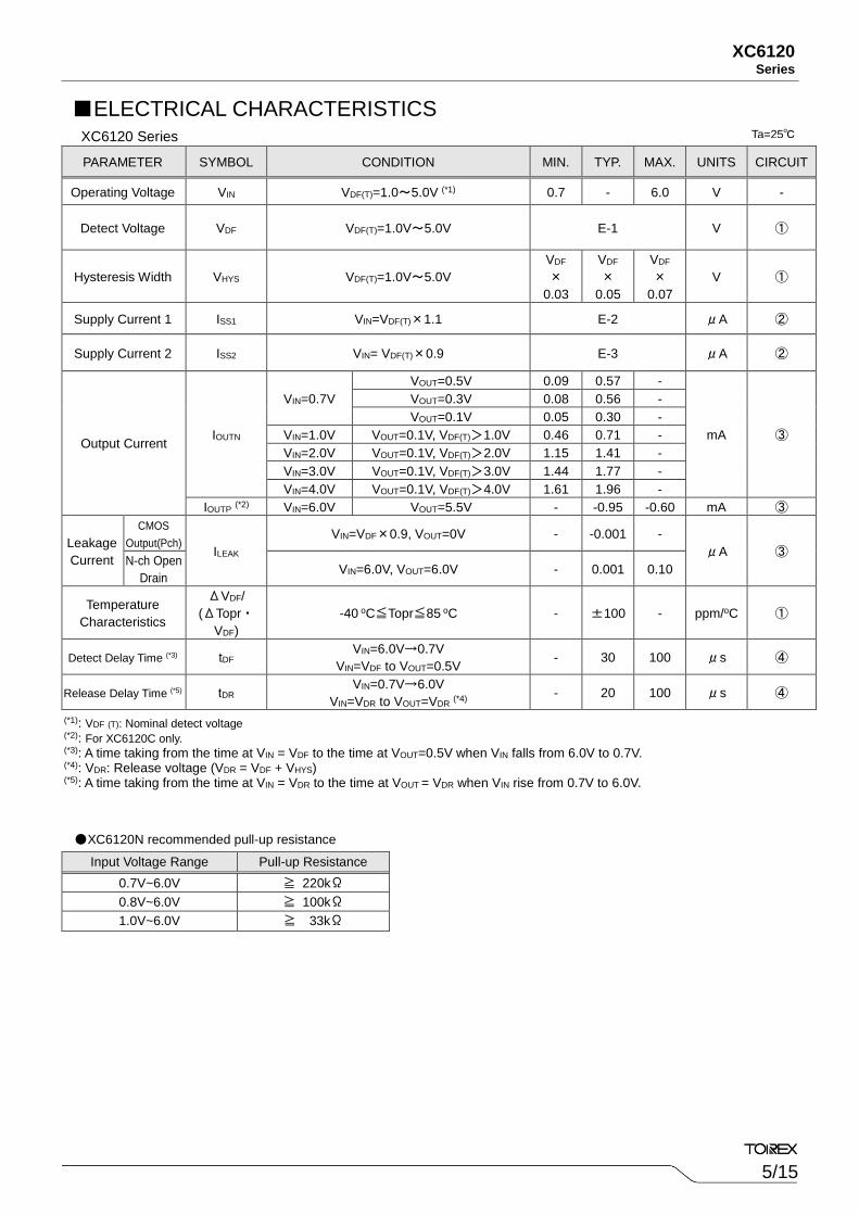
PARAMETER SYMBOL CONDITION MIN. TYP. MAX. UNITS CIRCUIT
Operating Voltage VIN VDF(T)=1.0~5.0V (*1) 0.7 - 6.0 V -
Detect Voltage VDF VDF(T)=1.0V~5.0V E-1 V ①
Hysteresis Width VHYS VDF(T)=1.0V~5.0V VDF
×
0.03
VDF ×
0.05
VDF ×
0.07 V ①
Supply Current 1 ISS1 VIN=VDF(T)×1.1 E-2 μA ②
Supply Current 2 ISS2 VIN= VDF(T)×0.9 E-3 μA ②
Output Current IOUTN
VIN=0.7V VOUT=0.5V 0.09 0.57 -
mA ③
VOUT=0.3V 0.08 0.56 - VOUT=0.1V 0.05 0.30 -
VIN=1.0V VOUT=0.1V, VDF(T)>1.0V 0.46 0.71 - VIN=2.0V VOUT=0.1V, VDF(T)>2.0V 1.15 1.41 - VIN=3.0V VOUT=0.1V, VDF(T)>3.0V 1.44 1.77 - VIN=4.0V VOUT=0.1V, VDF(T)>4.0V 1.61 1.96 -
IOUTP (*2) VIN=6.0V VOUT=5.5V - -0.95 -0.60 mA ③
Leakage Current
CMOS Output(Pch)
ILEAK VIN=VDF×0.9, VOUT=0V - -0.001 -
μA ③ N-ch Open
Drain VIN=6.0V, VOUT=6.0V - 0.001 0.10
Temperature Characteristics
ΔVDF/ (ΔTopr・
VDF) -40 oC≦Topr≦85 oC - ±100 - ppm/oC ①
Detect Delay Time (*3) tDF VIN=6.0V→0.7V
VIN=VDF to VOUT=0.5V - 30 100 μs ④
Release Delay Time (*5) tDR VIN=0.7V→6.0V
VIN=VDR to VOUT=VDR (*4) - 20 100 μs ④
Input Voltage Range Pull-up Resistance 0.7V~6.0V ≧ 220kΩ 0.8V~6.0V ≧ 100kΩ 1.0V~6.0V ≧ 33kΩ
■ELECTRICAL CHARACTERISTICS Ta=25℃ XC6120 Series
(*1): VDF (T): Nominal detect voltage (*2): For XC6120C only. (*3): A time taking from the time at VIN = VDF to the time at VOUT=0.5V when VIN falls from 6.0V to 0.7V. (*4): VDR: Release voltage (VDR = VDF + VHYS) (*5): A time taking from the time at VIN = VDR to the time at VOUT = VDR when VIN rise from 0.7V to 6.0V.
●XC6120N recommended pull-up resistance
6/15
XC6120 Series
SYMBOL E-1 E-2 E-3 PARAMETER DETECT VOLTAGE
VDF (V) XC6120xxx2 Series
SUPPLY CURRENT 1 ISS1 (μA)
SUPPLY CURRENT 2 ISS2 (μA)
NOMINAL DETECT
VOLTAGE VDF(T) MIN. MAX. TYP. MAX. TYP. MAX. 1.0 0.970 1.030
0.5 1.4 0.4 1.35
1.1 1.070 1.130 1.2 1.170 1.230 1.3 1.270 1.330 1.4 1.370 1.430 1.5 1.470 1.530 1.6 1.568 1.632 1.7 1.666 1.734 1.8 1.764 1.836 1.9 1.862 1.938 2.0 1.960 2.040
0.6 1.7 0.5 1.60
2.1 2.058 2.142 2.2 2.156 2.244 2.3 2.254 2.346 2.4 2.352 2.448 2.5 2.450 2.550 2.6 2.548 2.652 2.7 2.646 2.754 2.8 2.744 2.856
0.7 1.9 0.6 1.80
2.9 2.842 2.958 3.0 2.940 3.060 3.1 3.038 3.162 3.2 3.136 3.264 3.3 3.234 3.366 3.4 3.332 3.468 3.5 3.430 3.570 3.6 3.528 3.672 3.7 3.626 3.774 3.8 3.724 3.876 3.9 3.822 3.978 4.0 3.920 4.080 4.1 4.018 4.182 4.2 4.116 4.284 4.3 4.214 4.386 4.4 4.312 4.488 4.5 4.410 4.590 4.6 4.508 4.692 4.7 4.606 4.794 4.8 4.704 4.896 4.9 4.802 4.998 5.0 4.900 5.100
● DETECT VOLTAGE ACCURACY AND SUPPLY CURRENT SPECIFICATIONS
(*6)When detect voltage is 1.0V≦VDF(T)<1.5V, detect accuracy is ±30mV. When detect voltage is 1.5V≦VDF(T)≦5.0V, detect accuracy is ±2%.
■ELECTRICAL CHARACTERISTICS (Continued)
7/15
XC6120 Series
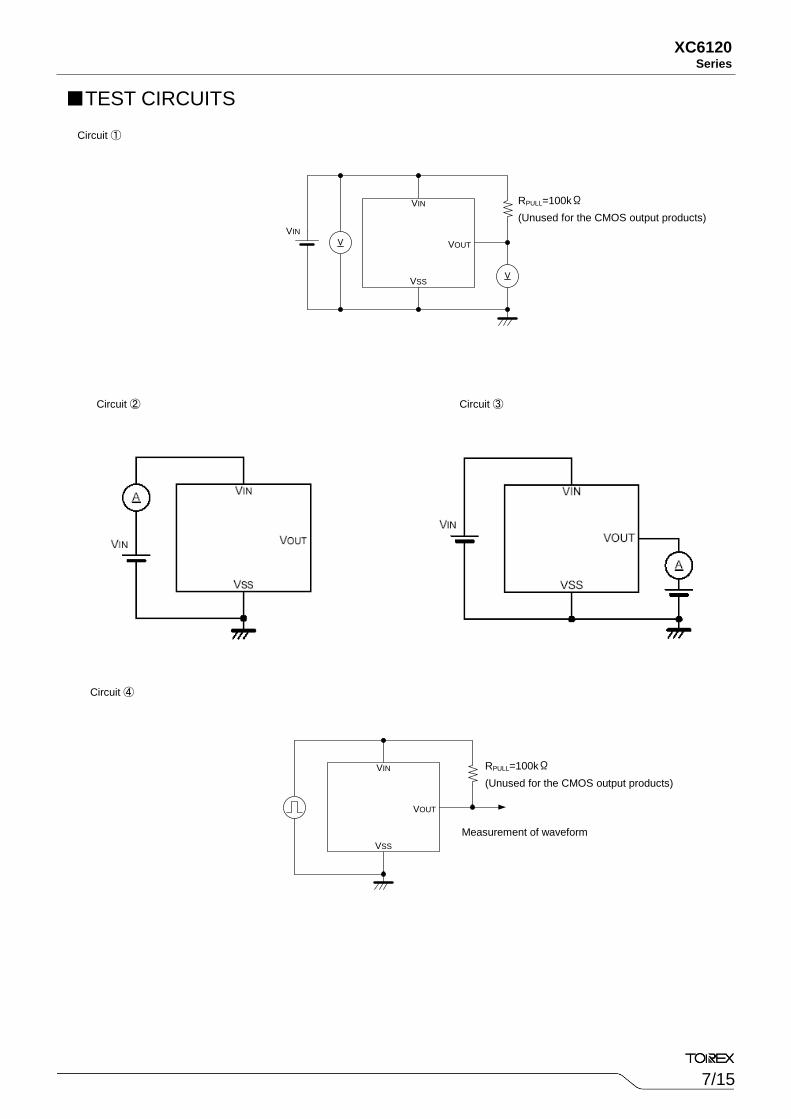
■TEST CIRCUITS Circuit ①
Circuit ② Circuit ③
Circuit ④
RPULL=100kΩ (Unused for the CMOS output products)
V
V
VIN
VOUT
VSS
VIN
Measurement of waveform
RPULL=100kΩ (Unused for the CMOS output products)
VIN
VOUT
VSS
8/15
XC6120 Series
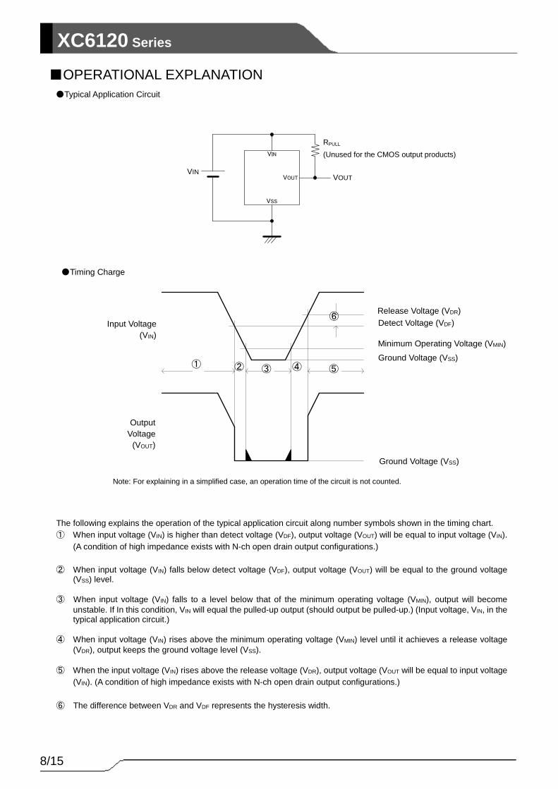
■OPERATIONAL EXPLANATION
The following explains the operation of the typical application circuit along number symbols shown in the timing chart. ① When input voltage (VIN) is higher than detect voltage (VDF), output voltage (VOUT) will be equal to input voltage (VIN).
(A condition of high impedance exists with N-ch open drain output configurations.) ② When input voltage (VIN) falls below detect voltage (VDF), output voltage (VOUT) will be equal to the ground voltage
(VSS) level.
③ When input voltage (VIN) falls to a level below that of the minimum operating voltage (VMIN), output will become unstable. If In this condition, VIN will equal the pulled-up output (should output be pulled-up.) (Input voltage, VIN, in the typical application circuit.)
④ When input voltage (VIN) rises above the minimum operating voltage (VMIN) level until it achieves a release voltage
(VDR), output keeps the ground voltage level (VSS). ⑤ When the input voltage (VIN) rises above the release voltage (VDR), output voltage (VOUT will be equal to input voltage
(VIN). (A condition of high impedance exists with N-ch open drain output configurations.) ⑥ The difference between VDR and VDF represents the hysteresis width.
●Timing Charge
●Typical Application Circuit
Note: For explaining in a simplified case, an operation time of the circuit is not counted.
VIN
VSS
VOUTVIN
VOUT
RPULL (Unused for the CMOS output products)
Input Voltage (VIN)
Output Voltage
(VOUT)
Release Voltage (VDR) Detect Voltage (VDF)
Minimum Operating Voltage (VMIN)
Ground Voltage (VSS)
Ground Voltage (VSS)
① ② ④ ③ ⑤
⑥
9/15
XC6120 Series
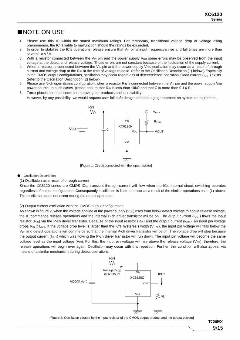
[Figure 1: Circuit connected with the input resistor] ● Oscillation Description
[Figure 2: Oscillation caused by the input resistor of the CMOS output product and the output current]
■NOTE ON USE 1. Please use this IC within the stated maximum ratings. For temporary, transitional voltage drop or voltage rising
phenomenon, the IC is liable to malfunction should the ratings be exceeded. 2. In order to stabilize the IC's operations, please ensure that VIN pin's input frequency's rise and fall times are more than
several μs / V. 3. With a resistor connected between the VIN pin and the power supply VDD some errors may be observed from the input
voltage at the detect and release voltage. Those errors are not constant because of the fluctuation of the supply current. 4. When a resistor is connected between the VIN pin and the power supply VDD, oscillation may occur as a result of through
current and voltage drop at the RIN at the time of voltage release. (refer to the Oscillation Description (1) below ) Especially in the CMOS output configurations, oscillation may occur regardless of detect/release operation if load current (IOUT) exists. (refer to the Oscillation Description (2) below)
5. Please use N-ch open drains configuration, when a resistor RIN is connected between the VIN pin and the power supply VDD power source. In such cases, please ensure that RIN is less than 10kΩ and that C is more than 0.1μF.
6. Torex places an importance on improving our products and its reliability. However, by any possibility, we would request user fail-safe design and post-aging treatment on system or equipment.
(1) Oscillation as a result of through current Since the XC6120 series are CMOS ICs, transient through current will flow when the IC's internal circuit switching operates regardless of output configuration. Consequently, oscillation is liable to occur as a result of the similar operations as in (1) above. This oscillation does not occur during the detect operation. (2) Output current oscillation with the CMOS output configuration As shown in figure 2, when the voltage applied at the power supply (VDD) rises from below detect voltage to above release voltage, the IC commence release operations and the internal P-ch driver transistor will be on. The output current (IOUT) flows the input resistor (RIN) via the P-ch driver transistor. Because of the input resistor (RIN) and the output current (IOUT), an input pin voltage drops RIN x IOUT. If the voltage drop level is larger than the IC’s hysteresis width (VHYS), the input pin voltage will falls below the VDF and detect operations will commerce so that the internal P-ch driver transistor will be off. The voltage drop will stop because the output current (IOUT) which was flowing the P-ch driver transistor will run down. The input pin voltage will become the same voltage level as the input voltage (VIN). For this, the input pin voltage will rise above the release voltage (VDR), therefore, the release operations will begin over again. Oscillation may occur with this repetition. Further, this condition will also appear via means of a similar mechanism during detect operations.
VIN
VSS
VOUTVDD
VOUT
RPULL-UP
RINVPULL-UP
CXC6120N
VIN
VSS
VOUTVDD(≧VDR)
RL
RIN
IOUTVoltage Drop(RIN×IOUT)
XC6120C
VPULL
RPULL
10/15
XC6120 Series
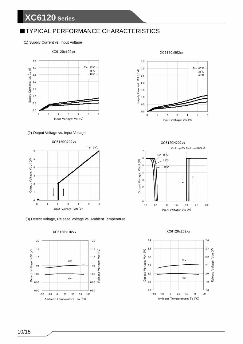
■TYPICAL PERFORMANCE CHARACTERISTICS (1) Supply Current vs. Input Voltage
XC6120x102xx
0.0
0.5
1.0
1.5
2.0
2.5
3.0
3.5
0 1 2 3 4 5 6
Input Voltage: VIN (V)
Supp
ly C
urr
ent:
IS
S (
μA
) Ta= 85℃
25℃
-40℃
XC6120x502xx
0.0
0.5
1.0
1.5
2.0
2.5
3.0
3.5
0 1 2 3 4 5 6
Input Voltage: VIN (V)
Supp
ly C
urr
ent:
IS
S (
μA
) Ta= 85℃
25℃
-40℃
(2) Output Voltage vs. Input Voltage
(3) Detect Voltage, Release Voltage vs. Ambient Temperature
XC6120x102xx
0.90
0.95
1.00
1.05
1.10
1.15
1.20
-50 -25 0 25 50 75 100
Ambient Temperature: Ta (℃)
Dete
ct
Volt
age: V
DF (
V)
0.90
0.95
1.00
1.05
1.10
1.15
1.20
Rele
ase V
olt
age: V
DR (
V)
VDR
VDF
XC6120x202xx
1.8
1.9
2.0
2.1
2.2
2.3
2.4
-50 -25 0 25 50 75 100
Ambient Temperature: Ta (℃)
Dete
ct
Volt
age: V
DF (
V)
1.8
1.9
2.0
2.1
2.2
2.3
2.4
Rele
ase V
olt
age: V
DR (
V)
VDR
VDF
XC6120C202xx
0
1
2
3
4
5
6
0 1 2 3 4 5 6
Input Voltage: VIN (V)
Outp
ut
Volt
age: V
OU
T (
V)
Ta= 25℃
XC6120N202xx
0
1
2
3
4
5
6
7
0.0 0.5 1.0 1.5 2.0 2.5 3.0
Input Voltage: VIN (V)
Outp
ut
Volt
age: V
OU
T (
V)
Ta= 85℃
Vpull-up=6V Rpull-up=100kΩ
25℃
-50℃
11/15
XC6120 Series
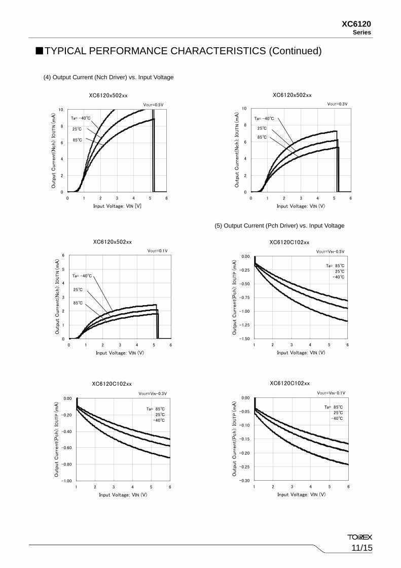
■TYPICAL PERFORMANCE CHARACTERISTICS (Continued)
(4) Output Current (Nch Driver) vs. Input Voltage
XC6120x502xx
0
2
4
6
8
10
0 1 2 3 4 5 6
Input Voltage: VIN [V]
Outp
ut
Curr
ent(
Nch): I
OU
TN (
mA
)
Ta= -40℃
VOUT=0.5V
25℃
85℃
XC6120x502xx
0
2
4
6
8
10
0 1 2 3 4 5 6
Input Voltage: VIN (V)
Outp
ut
Curr
ent(
Nch): I
OU
TN (
mA
)
Ta= -40℃
VOUT=0.3V
25℃
85℃
XC6120x502xx
0
1
2
3
4
5
6
0 1 2 3 4 5 6
Input Voltage: VIN (V)
Outp
ut
Curr
ent(
Nch): I
OU
TN (
mA
)
Ta= -40℃
VOUT=0.1V
25℃
85℃
XC6120C102xx
-1.50
-1.25
-1.00
-0.75
-0.50
-0.25
0.00
1 2 3 4 5 6
Input Voltage: VIN (V)
Outp
ut
Curr
ent(
Pch): I
OU
TP (
mA
)
Ta= 85℃
25℃
-40℃
VOUT=VIN-0.5V
(5) Output Current (Pch Driver) vs. Input Voltage
XC6120C102xx
-1.00
-0.80
-0.60
-0.40
-0.20
0.00
1 2 3 4 5 6
Input Voltage: VIN (V)
Outp
ut
Curr
ent(
Pch): I
OU
TP (
mA
)
Ta= 85℃
25℃
-40℃
VOUT=VIN-0.3V
XC6120C102xx
-0.30
-0.25
-0.20
-0.15
-0.10
-0.05
0.00
1 2 3 4 5 6
Input Voltage: VIN (V)
Outp
ut
Curr
ent(
Pch): I
OU
TP (
mA
)
Ta= 85℃
25℃
-40℃
VOUT=VIN-0.1V
12/15
XC6120 Series
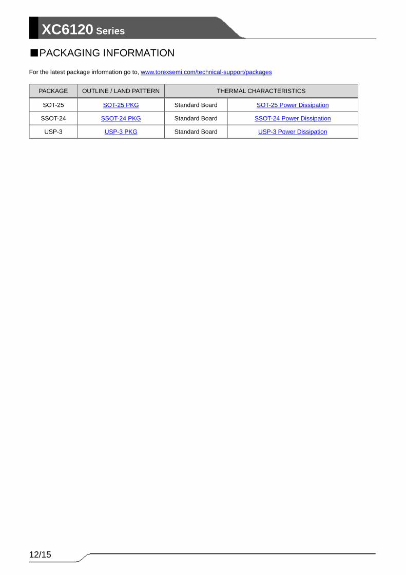
■PACKAGING INFORMATION
For the latest package information go to, www.torexsemi.com/technical-support/packages
PACKAGE OUTLINE / LAND PATTERN THERMAL CHARACTERISTICS
SOT-25 SOT-25 PKG Standard Board SOT-25 Power Dissipation
SSOT-24 SSOT-24 PKG Standard Board SSOT-24 Power Dissipation
USP-3 USP-3 PKG Standard Board USP-3 Power Dissipation
13/15
XC6120 Series
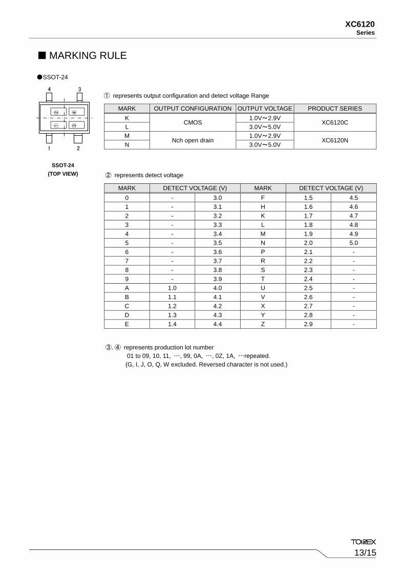
MARK OUTPUT CONFIGURATION OUTPUT VOLTAGE PRODUCT SERIES K
CMOS 1.0V~2.9V
XC6120C L 3.0V~5.0V M
Nch open drain 1.0V~2.9V
XC6120N N 3.0V~5.0V
MARK DETECT VOLTAGE (V) MARK DETECT VOLTAGE (V) 0 - 3.0 F 1.5 4.5 1 - 3.1 H 1.6 4.6 2 - 3.2 K 1.7 4.7 3 - 3.3 L 1.8 4.8 4 - 3.4 M 1.9 4.9 5 - 3.5 N 2.0 5.0 6 - 3.6 P 2.1 - 7 - 3.7 R 2.2 - 8 - 3.8 S 2.3 - 9 - 3.9 T 2.4 - A 1.0 4.0 U 2.5 - B 1.1 4.1 V 2.6 - C 1.2 4.2 X 2.7 - D 1.3 4.3 Y 2.8 - E 1.4 4.4 Z 2.9 -
■ MARKING RULE
●SSOT-24
① represents output configuration and detect voltage Range
② represents detect voltage
③,④ represents production lot number 01 to 09, 10, 11, …, 99, 0A, …, 0Z, 1A, …repeated.
(G, I, J, O, Q, W excluded. Reversed character is not used.)
SSOT-24 (TOP VIEW)
④
1 2
34
③
② ①
14/15
XC6120 Series
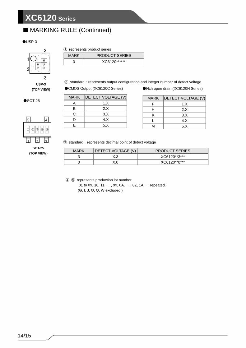
MARK PRODUCT SERIES 0 XC6120******
MARK DETECT VOLTAGE (V) PRODUCT SERIES 3 X.3 XC6120**3*** 0 X.0 XC6120**0***
MARK DETECT VOLTAGE (V) A 1.X B 2.X C 3.X D 4.X E 5.X
MARK DETECT VOLTAGE (V) F 1.X H 2.X K 3.X L 4.X M 5.X
●USP-3
③ standard:represents decimal point of detect voltage
② standard:represents output configuration and integer number of detect voltage
① represents product series
■ MARKING RULE (Continued)
1
2
3
3
②③
①
④⑤
USP-3 (TOP VIEW) ●CMOS Output (XC6120C Series)
●Nch open drain (XC6120N Series)
④,⑤ represents production lot number 01 to 09, 10, 11, …, 99, 0A, …, 0Z, 1A, …repeated.
(G, I, J, O, Q, W excluded.)
1 2 3
5 4
① ② ③ ④ ⑤
SOT-25 (TOP VIEW)
●SOT-25
15/15
XC6120 Series
1. The product and product specifications contained herein are subject to change without notice to improve performance characteristics. Consult us, or our representatives before use, to confirm that the information in this datasheet is up to date.
2. The information in this datasheet is intended to illustrate the operation and characteristics of our
products. We neither make warranties or representations with respect to the accuracy or completeness of the information contained in this datasheet nor grant any license to any intellectual property rights of ours or any third party concerning with the information in this datasheet.
3. Applicable export control laws and regulations should be complied and the procedures required by
such laws and regulations should also be followed, when the product or any information contained in this datasheet is exported.
4. The product is neither intended nor warranted for use in equipment of systems which require
extremely high levels of quality and/or reliability and/or a malfunction or failure which may cause loss of human life, bodily injury, serious property damage including but not limited to devices or equipment used in 1) nuclear facilities, 2) aerospace industry, 3) medical facilities, 4) automobile industry and other transportation industry and 5) safety devices and safety equipment to control combustions and explosions. Do not use the product for the above use unless agreed by us in writing in advance.
5. Although we make continuous efforts to improve the quality and reliability of our products;
nevertheless Semiconductors are likely to fail with a certain probability. So in order to prevent personal injury and/or property damage resulting from such failure, customers are required to incorporate adequate safety measures in their designs, such as system fail safes, redundancy and fire prevention features.
6. Our products are not designed to be Radiation-resistant.
7. Please use the product listed in this datasheet within the specified ranges.
8. We assume no responsibility for damage or loss due to abnormal use.
9. All rights reserved. No part of this datasheet may be copied or reproduced unless agreed by Torex
Semiconductor Ltd in writing in advance.
TOREX SEMICONDUCTOR LTD.