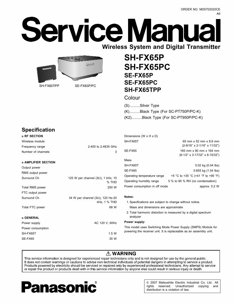
Wireless System and Digital Transmitter SH-FX65P SH...
65
n RF SECTION Wireless module Frequency range 2.400 to 2.4835 GHz Number of channels 3 n AMPLIFIER SECTION Output power RMS output power Surround Ch 125 W per channel (3Ω), 1 kHz, 10 % THD Total RMS power 250 W FTC output power Surround Ch 34 W per channel (3Ω), 120 Hz-20 kHz, 1 % THD Total FTC power 68 W n GENERAL Power supply AC 120 V, 60Hz Power consumption SH-FX65T 1.5 W SE-FX65 35 W © 2007 Matsushita Electric Industrial Co. Ltd.. All rights reserved. Unauthorized copying and distribution is a violation of law. SH-FX65P SH-FX65PC SE-FX65P SE-FX65PC SH-FX65TPP Colour (S)..........Silver Type (K)..........Black Type (For SC-PT750P/PC-K) (K2)..........Black Type (For SC-PT950P/PC-K) Dimensions (W x H x D) SH-FX65T 65 mm x 52 mm x 8.6 mm (2-9/16” x 2-1/16” x 11/32”) SE-FX65 165 mm x 90 mm x 164 mm (6-1/2” x 3-17/32” x 6-15/32”) Mass SH-FX65T 0.02 kg (0.04 lbs) SE-FX65 0.655 kg (1.54 lbs) Operating temperature range +5 °C to +35 °C (+41 °F to +95 °F) Operating humidity range 5 % to 90 % RH (no condensation) Power consumption in off mode approx. 0.2 W Notes: 1. Specifications are subject to change without notice. Mass and dimensions are approximate 2. Total harmonic distortion is measured by a digital spectrum analyzer Power supply: This model uses Switching Mode Power Supply (SMPS) Module for powering the receiver unit. It is replaceable as an assembly unit. Wireless System and Digital Transmitter Specification ORDER NO. MD0702020CE A6
-
Upload
hoangnguyet -
Category
Documents
-
view
254 -
download
1
Transcript of Wireless System and Digital Transmitter SH-FX65P SH...
n RF SECTIONWireless module
Frequency range 2.400 to 2.4835 GHz
Number of channels 3
n AMPLIFIER SECTIONOutput power
RMS output power
Surround Ch 125 W per channel (3Ω), 1 kHz, 10% THD
Total RMS power 250 W
FTC output power
Surround Ch 34 W per channel (3Ω), 120 Hz-20kHz, 1 % THD
Total FTC power 68 W
n GENERALPower supply AC 120 V, 60Hz
Power consumption
SH-FX65T 1.5 W
SE-FX65 35 W
© 2007 Matsushita Electric Industrial Co. Ltd.. Allrights reserved. Unauthorized copying anddistribution is a violation of law.
SH-FX65PSH-FX65PCSE-FX65PSE-FX65PCSH-FX65TPPColour(S)..........Silver Type(K)..........Black Type (For SC-PT750P/PC-K)(K2)..........Black Type (For SC-PT950P/PC-K)
Dimensions (W x H x D)
SH-FX65T 65 mm x 52 mm x 8.6 mm(2-9/16” x 2-1/16” x 11/32”)
SE-FX65 165 mm x 90 mm x 164 mm(6-1/2” x 3-17/32” x 6-15/32”)
Mass
SH-FX65T 0.02 kg (0.04 lbs)
SE-FX65 0.655 kg (1.54 lbs)
Operating temperature range +5 °C to +35 °C (+41 °F to +95 °F)
Operating humidity range 5 % to 90 % RH (no condensation)
Power consumption in off mode approx. 0.2 W
Notes: 1. Specifications are subject to change without notice.
Mass and dimensions are approximate
2. Total harmonic distortion is measured by a digital spectrumanalyzer
Power supply:This model uses Switching Mode Power Supply (SMPS) Module forpowering the receiver unit. It is replaceable as an assembly unit.
Wireless System and Digital Transmitter
Specification
ORDER NO. MD0702020CEA6
1 Note 3 1.1. System Combination Breakdown 3
1.2. Packaging 3
2 Safety Precautions 4 2.1. GENERAL GUIDELINES 4
2.2. Before Repair and Adjustment (Digital Receiver SE-FX65)
4
2.3. Protection Circuitry 5
2.4. Safety Part Information 5
3 Prevention of Electro Static Discharge (ESD) toElectrostatically Sensitive (ES) Devices 6
4 Handling the Lead-free Solder 7 4.1. Service caution based on legal restrictions 7
5 Accessories 8 6 Using of Digital Receiver Unit 9
6.1. Connecting the digital transmitter (SH-FX65T) 9
6.2. Connecting the surround speaker cables to the wireless
system (SE-FX65) 9
6.3. AC Power Cord connection (SE-FX65) 9
6.4. Making the wireless link (SE-FX65) 10
7 Operation Procedures 11 7.1. Remote Control Key Buttons Operations 11
7.2. Main Unit Key Buttons Operations 12
8 New Features 13 8.1. Wireless Features 13
9 Self-Diagnosis and Special Mode Setting 20 9.1. Wireless Service Mode Summary Table 20
9.2. Service Mode Table (Wireless) 21
10 Assembling and Disassembling 23 10.1. Note 23
10.2. Disassembly flow chart (For SE-FX65) 24
10.3. Main Parts Location Diagram 24
10.4. Disassembly of Wireless System (SE-FX65P/PC) 25
10.5. Disassembly of Transmitter Module P.C.B (SH-FX65T) 28
11 Service Positions 29
11.1. Checking of Led, Led Drive, DAMP and Receiver Module
P.C.B. 29
12 Voltage Measurement & Waveform Chart 30 12.1. Voltage Measurement 30
12.2. Waveform Chart 31
13 Wiring Connection Diagram 32 14 Block Diagram 33
14.1. DIGITAL AMPLIFIER/LED DRIVE/LED BLOCK DIAGRAM
33
14.2. RECEIVER MODULE BLOCK DIAGRAM 34
14.3. TRANSMITTER MODULE BLOCK DIAGRAM 35
15 Notes of Schematic Diagram 37 16 Schematic Diagram 39
16.1. DAMP CIRCUIT, LED DRIVE CIRCUIT and LED CIRCUIT
39
16.2. RECEIVER MODULE CIRCUIT 41
16.3. TRANSMITTER MODULE CIRCUIT 45
17 Printed Circuit Board Diagram 49 17.1. DAMP P.C.B, LED DRIVE P.C.B, LED P.C.B and
RECEIVER MODULE P.C.B 49
17.2. TRANSMITTER MODULE P.C.B 50
18 Illustration of IC's, Transistors and Diodes 51 19 Terminal Functions of Integrated Circuits 52
19.1. IC10 (C1AB00002772): IC BASE BAND 52
19.2. IC13 (C1CB00002648): IC RF 52
19.3. IC1000 (C2BBED000056): IC MCU 53
20 Exploded Views 55 20.1. Cabinet Parts Location 55
20.2. Packaging 56
21 Service Hint 59 21.1. TX / RX KIT ASSEMBLY 59
21.2. TX CASE ASSEMBLY 59
22 Replacement Parts List 60 22.1. Parts List (SE-FX65) 60
22.2. Parts List (SH-FX65T) 63
CONTENTS Page Page
2
SH-FX65P / SH-FX65PC
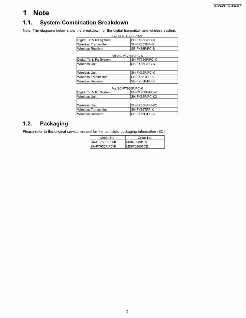
1 Note1.1. System Combination BreakdownNote: The diagrams below show the breakdown for the digital transmitter and wireless system.
For SH-FX65P/PC-SDigital Tx & Rx System SH-FX65P/PC-SWireless Transmitter SH-FX65TPP-SWireless Receiver SE-FX65P/PC-S
For SC-PT750P/PC-KDigital Tx & Rx System SH-PT750P/PC-KWireless Unit SH-FX65P/PC-K
Wireless Unit SH-FX65P/PC-KWireless Transmitter SH-FX65TPP-KWireless Receiver SE-FX65P/PC-K
For SC-PT950P/PC-KDigital Tx & Rx System SH-PT950P/PC-KWireless Unit SH-FX65P/PC-K2
Wireless Unit SH-FX65P/PC-K2Wireless Transmitter SH-FX65TPP-KWireless Receiver SE-FX65P/PC-K
1.2. PackagingPlease refer to the original service manual for the complete packaging information (SC)
Model No. Order No.SA-PT750P/PC-K MD0702001CESA-PT950P/PC-K MD0702003CE
3
SH-FX65P / SH-FX65PC
(This “Safety Precaution” is applied only in U.S.A.)
2 Safety Precautions2.1. GENERAL GUIDELINES 1. When servicing, observe the original lead dress. If a short circuit is found, replace all parts which have been overheated or
damaged by the short circuit. 2. After servicing, see to it that all the protective devices such as insulation barriers, insulation papers shields are properly
installed. 3. After servicing, make the following leakage current checks to prevent the customer from being exposed to shock hazards.
1. Before servicing, unplug the power cord to prevent an electric shock. 2. When replacing parts, use only manufacturer’s recommended components for safety. 3. Check the condition of the power cord. Replace if wear or damage is evident. 4. After servicing, be sure to restore the lead dress, insulation barriers, insulation papers, shields, etc. 5. Before returning the serviced equipment to the customer, be sure to make the following insulation resistance test to prevent the
customer from being exposed to a shock hazard.
2.1.1. LEAKAGE CURRENT COLD CHECK 1. Unplug the AC cord and connect a jumper between the two prongs on the plug. 2. Measure the resistance value, with an ohmmeter, between the jumpered AC plug and each exposed metallic cabinet part on
the equipment such as screwheads, connectors, control shafts, etc. When the exposed metallic part has a return path to thechassis, the reading should be between 1MΩ and 5.2Ω.When the exposed metal does not have a return path to the chassis, the reading must be .
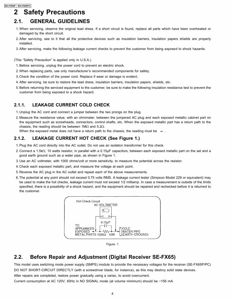
2.1.2. LEAKAGE CURRENT HOT CHECK (See Figure 1.) 1. Plug the AC cord directly into the AC outlet. Do not use an isolation transformer for this check. 2. Connect a 1.5kΩ, 10 watts resistor, in parallel with a 0.15µF capacitors, between each exposed metallic part on the set and a
good earth ground such as a water pipe, as shown in Figure 1. 3. Use an AC voltmeter, with 1000 ohms/volt or more sensitivity, to measure the potential across the resistor. 4. Check each exposed metallic part, and measure the voltage at each point. 5. Reverse the AC plug in the AC outlet and repeat each of the above measurements. 6. The potential at any point should not exceed 0.75 volts RMS. A leakage current tester (Simpson Model 229 or equivalent) may
be used to make the hot checks, leakage current must not exceed 1/2 milliamp. In case a measurement is outside of the limitsspecified, there is a possibility of a shock hazard, and the equipment should be repaired and rechecked before it is returned tothe customer.
Figure. 1
2.2. Before Repair and Adjustment (Digital Receiver SE-FX65)This model uses switching mode power supply (SMPS) module to provide the necessary voltages for the receiver (SE-FX65P/PC)DO NOT SHORT-CIRCUIT DIRECTLY (with a screwdriver blade, for instance), as this may destroy solid state devices.After repairs are completed, restore power gradually using a variac, to avoid overcurrent.Current consumption at AC 120V, 60Hz in NO SIGNAL mode (at volume minimum) should be ~156 mA.
4
SH-FX65P / SH-FX65PC
2.3. Protection CircuitryThe protection circuitry may have operated if either of the following conditions are noticed: · No sound is heard when the power is turned on. · Stops during a performance.
The function of this circuitry is to prevent circuitry damage if, for example, the positive and negative speaker connection wires are“shorted”, or if speaker systems with an impedance less than the indicated rated impedance of the amplifier are used.If this occurs, follow the procedure outlines below: 1. Turn off the power. 2. Determine the cause of the problem and correct it. 3. Turn on the power once again after one minute.
Note:When the protection circuitry functions, the unit will not operate unless the power is first turned off and then on again.
2.4. Safety Part InformationSafety Parts List:
There are special components used in this equipment which are important for safety.These parts are marked by in theSchematic Diagrams & Replacement Parts List. It is essential that these critical partsshould be replaced with manufacturer’sspecified parts to prevent shock, fire or other hazards. Do not modify the original designwithout permission of manufacturer.
Table 1Reference No. Part No. Part Name & Description Remarks
A1 K2CB2CB00018 AC CORD18 N0AB6GY00001 SMPS MODULE
5
SH-FX65P / SH-FX65PC
3 Prevention of Electro Static Discharge (ESD) toElectrostatically Sensitive (ES) Devices
Some semiconductor (solid state) devices can be damaged easily by electricity. Such components commonly are calledElectrostatically Sensitive (ES) Devices. Examples of typical ES devices are integrated circuits and some field-effect transistors andsemiconductor “chip” components. The following techniques should be used to help reduce the incidence of component damagecaused by electro static discharge (ESD). 1. Immediately before handling any semiconductor component or semiconductor-equiped assembly, drain off any ESD on your
body by touching a known earth ground. Alternatively, obtain and wear a commercially available discharging ESD wrist strap,which should be removed for potential shock reasons prior to applying power to the unit under test.
2. After removing an electrical assembly equiped with ES devices, place the assembly on a conductive surface such as aluminiumfoil, to prevent electrostatic charge build up or exposure of the assembly.
3. Use only a grounded-tip soldering iron to solder or unsolder ES devices. 4. Use only an anti-static solder removal device. Some solder removal devices not classified as “anti-static (ESD protected)” can
generate electrical charge to damage ES devices. 5. Do not use freon-propelled chemicals. These can generate electrical charges sufficient to damage ES devices. 6. Do not remove a replacement ES device from its protective package until immediately before you are ready to install it. (Most
replacement ES devices are packaged with leads electrically shorted together by conductive foam, aluminium foil orcomparable conductive material).
7. Immediately before removing the protective material from the leads of a replacement ES device, touch the protective materialto the chassis or circuit assembly into which the device will be installed.Caution
Be sure no power is applied to the chassis or circuit, and observe all other safety precautions. 8. Minimize bodily motions when handling unpackaged replacement ES devices. (Otherwise harmless motion such as the
brushing together of your clothes fabric or the lifting of your foot from a carpeted floor can generate static electricity (ESD)sufficient to damage an ES device).
6
SH-FX65P / SH-FX65PC
4 Handling the Lead-free Solder4.1. Service caution based on legal restrictions4.1.1. General description about Lead Free Solder (PbF)The lead free solder has been used in the mounting process of all electrical components on the printed circuit boards used for thisequipment in considering the globally environmental conservation.
The normal solder is the alloy of tin (Sn) and lead (Pb). On the other hand, the lead free solder is the alloy mainly consists of tin(Sn), silver (Ag) and Copper (Cu), and the melting point of the lead free solder is higher approx.30 degrees C (86°F) more than thatof the normal solder.
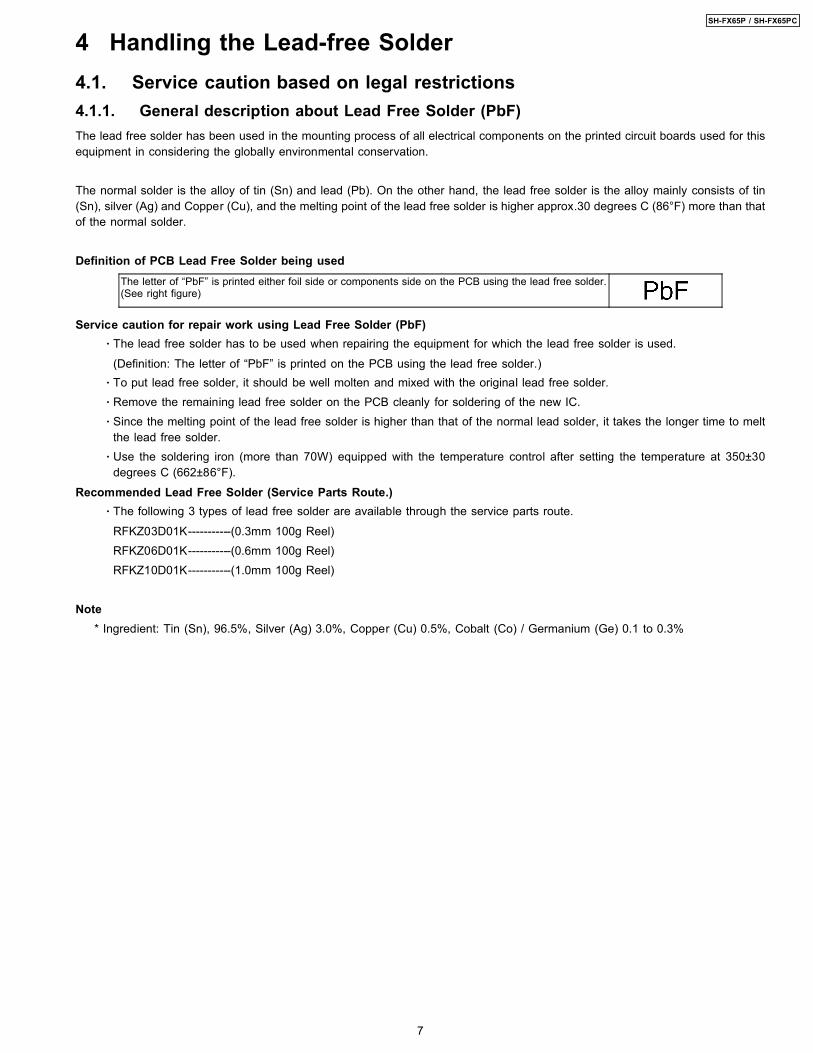
Definition of PCB Lead Free Solder being usedThe letter of “PbF” is printed either foil side or components side on the PCB using the lead free solder.(See right figure)
Service caution for repair work using Lead Free Solder (PbF) · The lead free solder has to be used when repairing the equipment for which the lead free solder is used.
(Definition: The letter of “PbF” is printed on the PCB using the lead free solder.) · To put lead free solder, it should be well molten and mixed with the original lead free solder. · Remove the remaining lead free solder on the PCB cleanly for soldering of the new IC. · Since the melting point of the lead free solder is higher than that of the normal lead solder, it takes the longer time to melt
the lead free solder. · Use the soldering iron (more than 70W) equipped with the temperature control after setting the temperature at 350±30
degrees C (662±86°F).Recommended Lead Free Solder (Service Parts Route.)
· The following 3 types of lead free solder are available through the service parts route.
RFKZ03D01K-----------(0.3mm 100g Reel)RFKZ06D01K-----------(0.6mm 100g Reel)RFKZ10D01K-----------(1.0mm 100g Reel)
Note* Ingredient: Tin (Sn), 96.5%, Silver (Ag) 3.0%, Copper (Cu) 0.5%, Cobalt (Co) / Germanium (Ge) 0.1 to 0.3%
7
SH-FX65P / SH-FX65PC
5 AccessoriesNote : Refer to Packing Materials & Accessories Parts List (Section 22) for the part number.
AC Power Cord
8
SH-FX65P / SH-FX65PC
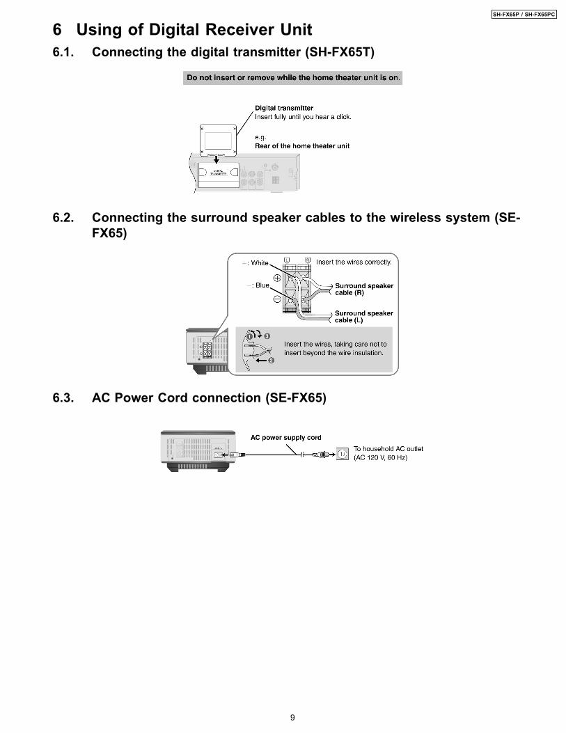
6 Using of Digital Receiver Unit6.1. Connecting the digital transmitter (SH-FX65T)
6.2. Connecting the surround speaker cables to the wireless system (SE-FX65)
6.3. AC Power Cord connection (SE-FX65)
9
SH-FX65P / SH-FX65PC
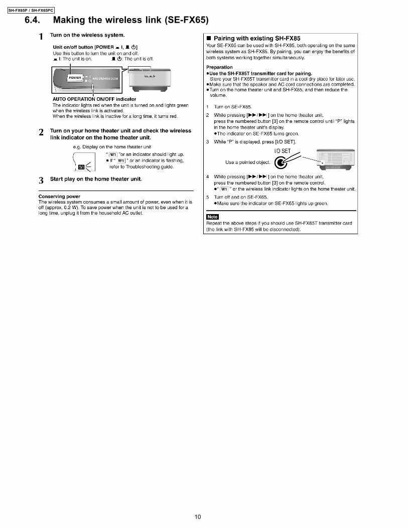
6.4. Making the wireless link (SE-FX65)
10
SH-FX65P / SH-FX65PC
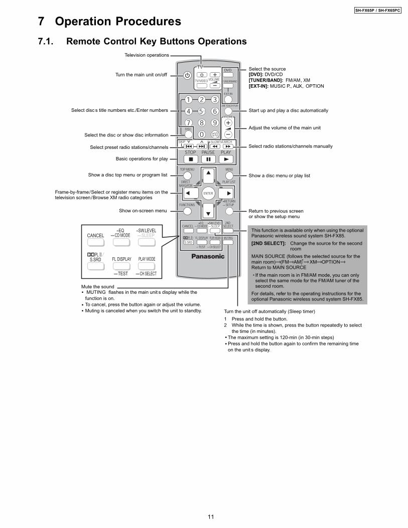
7 Operation Procedures7.1. Remote Control Key Buttons Operations
This function is available only when using the optional Panasonic wireless sound system SH-FX85.
[2ND SELECT]: Change the source for the second room
MAIN SOURCE (follows the selected source for the main room) (FM AM) XM OPTIONReturn to MAIN SOURCE
If the main room is in FM/AM mode, you can only select the same mode for the FM/AM tuner of the second room.
For details, refer to the operating instructions for the optional Panasonic wireless sound system SH-FX85.
CANCEL -CD MODE-EQ
-SLEEP-SW.LEVEL
FL DISPLAY PLAY MODE
-CH SELECT-TEST
PLS.SRD
Select disc s title numbers etc./Enter numbers
Basic operations for play
Show a disc top menu or program list
Show on-screen menu
Show a disc menu or play list
Return to previous screen or show the setup menu
Select the disc or show disc information
Turn the unit off automatically (Sleep timer)
1 Press and hold the button. 2 While the time is shown, press the button repeatedly to select
the time (in minutes).The maximum setting is 120-min (in 30-min steps)Press and hold the button again to confirm the remaining time on the unit s display.
Start up and play a disc automatically
Select preset radio stations/channels
Select the source[DVD]: DVD/CD [TUNER/BAND]: FM/AM , XM [EXT-IN]: MUSIC P. , AUX , OPTION
Frame-by-frame/Select or register menu items on thetelevision screen /Browse XM radio categories
Select radio stations/channels manually
Mute the soundMUTING flashes in the main unit s display while the
function is on.To cancel, press the button again or adjust the volume.Muting is canceled when you switch the unit to standby.
Adjust the volume of the main unit
Turn the main unit on/off
Television operations
*
*
11
SH-FX65P / SH-FX65PC
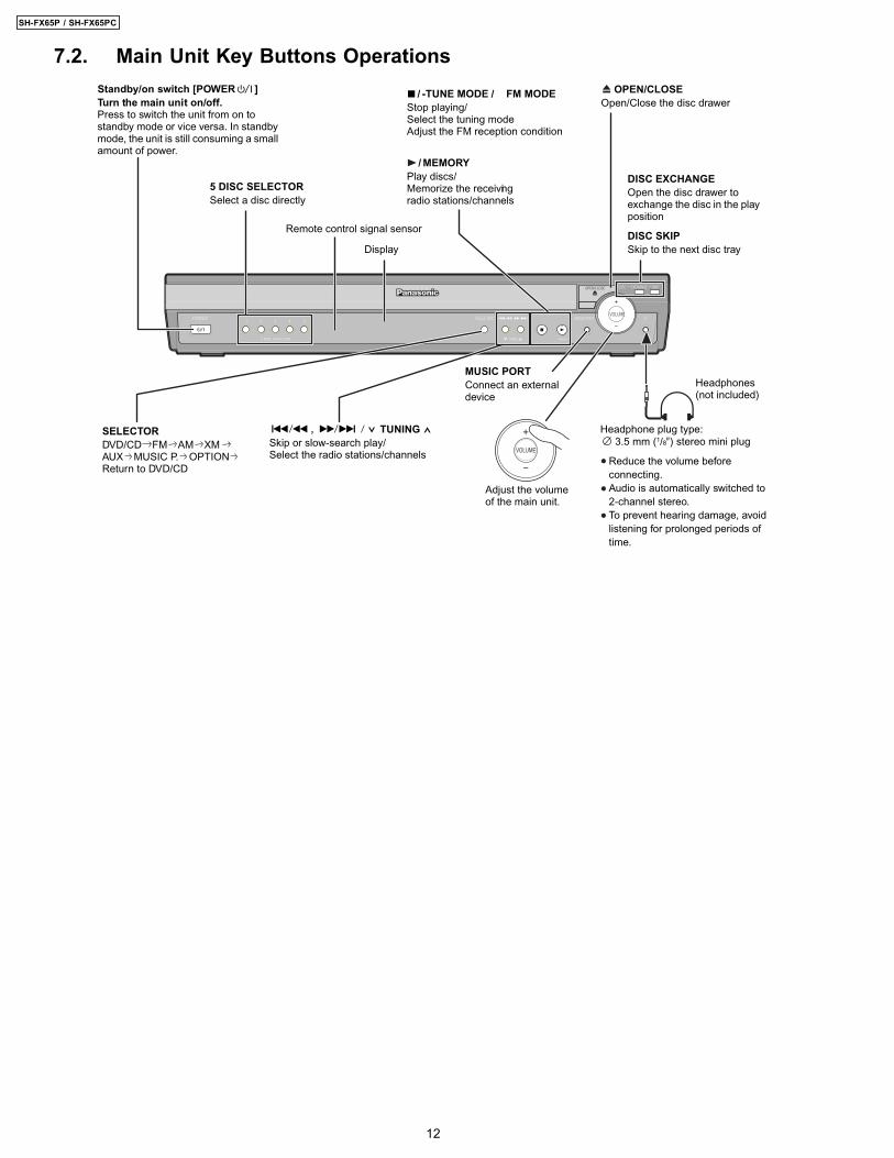
7.2. Main Unit Key Buttons Operations
VOLUME
MUSIC PORTConnect an external device
Skip or slow-search play/Select the radio stations/channels
5 DISC SELECTORSelect a disc directly
SELECTORDVD/CD FM AM XMAUX MUSIC P. OPTIONReturn to DVD/CD
Display
DISC EXCHANGEOpen the disc drawer to exchange the disc in the play position
DISC SKIPSkip to the next disc tray
Headphones(not included)
Remote control signal sensor
Adjust the volume of the main unit.
TUNING, Headphone plug type:3.5 mm (1/8 ) stereo mini plug
Reduce the volume before connecting.
Audio is automatically switched to 2-channel stereo.
To prevent hearing damage, avoid listening for prolonged periods of time.
"
OPEN/CLOSEOpen/Close the disc drawer
/ -TUNE MODE / FM MODEStop playing/ Select the tuning modeAdjust the FM reception condition
Play discs/Memorize the receivngiradio stations/channels
/ MEMORY
Turn the main unit on/off.Press to switch the unit from on to standby mode or vice versa. In standby mode, the unit is still consuming a small amount of power.
Standby/on switch [POWER ]
12
SH-FX65P / SH-FX65PC
8 New Features8.1. Wireless Features8.1.1. Function OverviewYear 2007 PT models support wireless which includes FX65/FX66, wireless subwoofer and FX85 as described below:-
8.1.1.1. FX65/FX66 · The FX65/FX66 supports one-way wireless transmission only, that is, it will only transmit wireless audio signal to the rear
surround speakers. The FX65/FX66 receiver module includes a D-AMP and SMPS. The transmitter interfaces with the main unitusing serial communications to communicate information such as mute command request, link detection and ID setting request.Maximum range attainable is 15 meters.
8.1.1.2. Wireless Subwoofer (For PT1050 only) · The wireless subwoofer receiver module is similar in operation with FX65/FX66 in such a way that it only supports one-way
wireless transmission. It also includes a D-AMP and SMPS. The difference in the wireless subwoofer receiver module is the wayits hardware interprets the audio it receives from the transmitter since it is the same audio received by the FX65/FX66 receiver.Maximum range attainable is 30 meters.
8.1.1.3. FX85 · The FX85 supports the multi-room function wherein it operates as a second room wireless receiver (up to a maximum of two).
Maximum range attainable is 30 meters. It can send commands to the main unit to control functions such as Play, Stop,Forward Skip/Channel Up, Reverse Skip/Channel Down. It also has a built-in DAP pocket for stand-alone operation by insertinga DAP device (e.g. iPod) in the DAP pocket to play the device only via the device’s own control buttons, FX85 cannot controlthe device using its own buttons. The transmitter interfaces with the main unit using serial communications to communicateinformation such as mute command request, link detection, ID setting request and button commands from the FX85 buttons(Play, Stop, Forward Skip/Channel Up, Reverse Skip/Channel Down). The FX85 receiver module has the followingfunctions/terminals/buttons:
FX85 BUTTONS FX85 FUNCTIONSFX 85 Power Button D-AmpSelector Button SMPSPlay Button D-Port ConnectorStop Button ID Set SwitchForward Skip/Channel Up MPortReverse Skip/Channel DownVolume Control
8.1.2. Block Diagram · There are two types of transmitter cards, Type A and Type B, and two types of receiver modules, Type 1 and Type 2 for the
wireless configuration. The block diagrams below describe the differences of each of the types.
13
SH-FX65P / SH-FX65PC
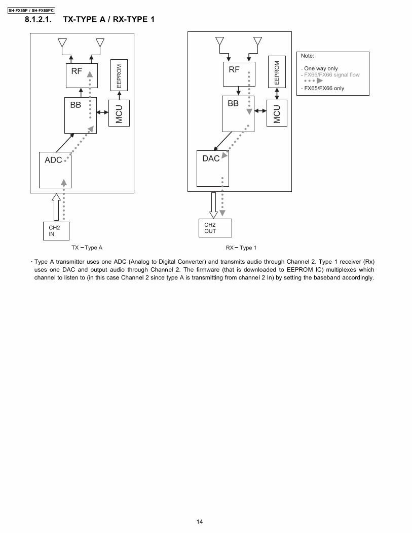
8.1.2.1. TX-TYPE A / RX-TYPE 1
ADC
BB
RF
MC
U
EE
PR
OM
CH2 IN
DAC
BB
RF
EE
PR
OM
CH2 OUT
Note: - One way only - FX65/FX66 signal flow
- FX65/FX66 only
TX Type A RX Type 1
MC
U
· Type A transmitter uses one ADC (Analog to Digital Converter) and transmits audio through Channel 2. Type 1 receiver (Rx)uses one DAC and output audio through Channel 2. The firmware (that is downloaded to EEPROM IC) multiplexes whichchannel to listen to (in this case Channel 2 since type A is transmitting from channel 2 In) by setting the baseband accordingly.
14
SH-FX65P / SH-FX65PC
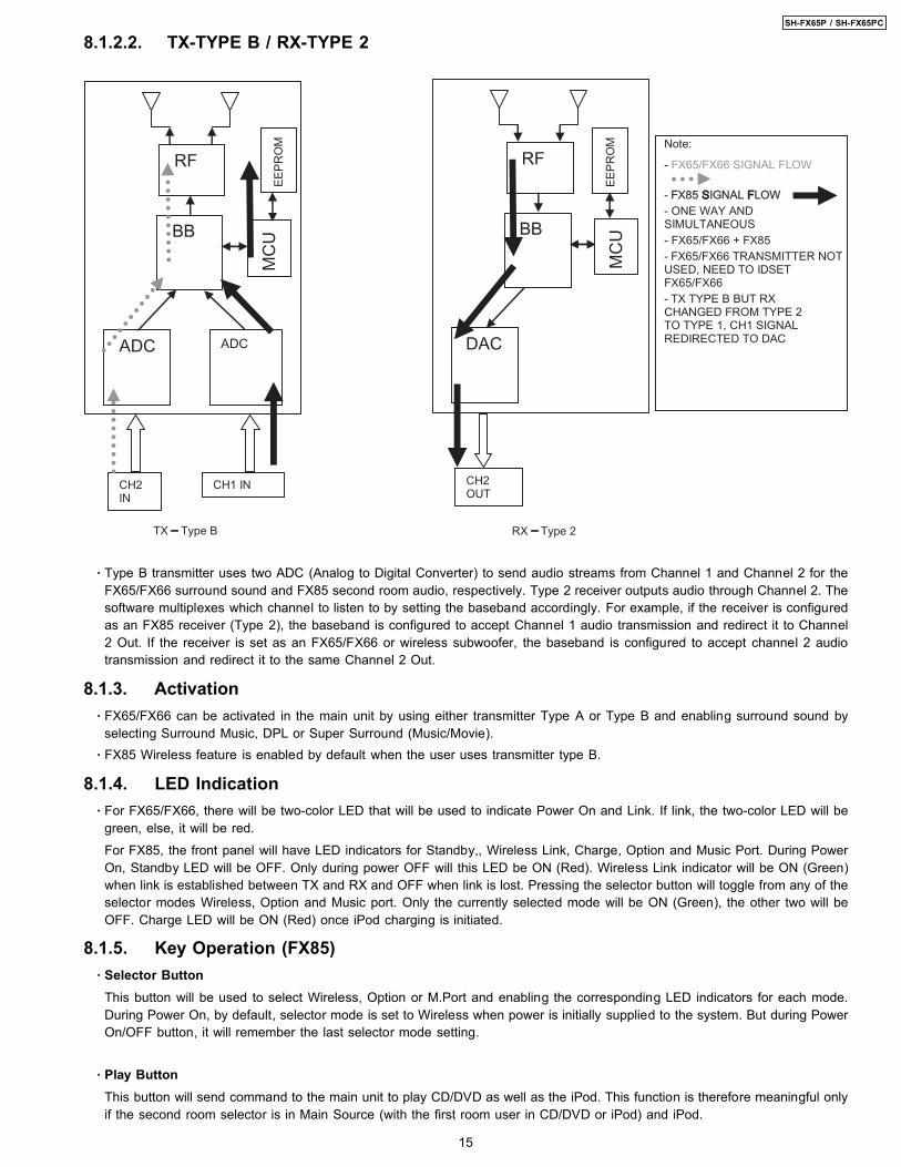
8.1.2.2. TX-TYPE B / RX-TYPE 2
ADC
BB
RF
MC
U
EE
PR
OM
ADC DAC
BB
RF
EE
PR
OM
MC
U
CH2 IN
CH1 IN CH2 OUT
Note: - FX65/FX66 SIGNAL FLOW
- FX85 SSIGNAL FFLOW
- ONE WAY AND SIMULTANEOUS
- FX65/FX66 + FX85
- FX65/FX66 TRANSMITTER NOT
USED, NEED TO IDSET FX65/FX66
- TX TYPE B BUT RX
CHANGED FROM TYPE 2 TO TYPE 1, CH1 SIGNAL REDIRECTED TO DAC
TX Type B RX Type 2
· Type B transmitter uses two ADC (Analog to Digital Converter) to send audio streams from Channel 1 and Channel 2 for theFX65/FX66 surround sound and FX85 second room audio, respectively. Type 2 receiver outputs audio through Channel 2. Thesoftware multiplexes which channel to listen to by setting the baseband accordingly. For example, if the receiver is configuredas an FX85 receiver (Type 2), the baseband is configured to accept Channel 1 audio transmission and redirect it to Channel2 Out. If the receiver is set as an FX65/FX66 or wireless subwoofer, the baseband is configured to accept channel 2 audiotransmission and redirect it to the same Channel 2 Out.
8.1.3. Activation · FX65/FX66 can be activated in the main unit by using either transmitter Type A or Type B and enabling surround sound by
selecting Surround Music, DPL or Super Surround (Music/Movie). · FX85 Wireless feature is enabled by default when the user uses transmitter type B.
8.1.4. LED Indication · For FX65/FX66, there will be two-color LED that will be used to indicate Power On and Link. If link, the two-color LED will be
green, else, it will be red.For FX85, the front panel will have LED indicators for Standby,, Wireless Link, Charge, Option and Music Port. During PowerOn, Standby LED will be OFF. Only during power OFF will this LED be ON (Red). Wireless Link indicator will be ON (Green)when link is established between TX and RX and OFF when link is lost. Pressing the selector button will toggle from any of theselector modes Wireless, Option and Music port. Only the currently selected mode will be ON (Green), the other two will beOFF. Charge LED will be ON (Red) once iPod charging is initiated.
8.1.5. Key Operation (FX85) · Selector Button
This button will be used to select Wireless, Option or M.Port and enabling the corresponding LED indicators for each mode.During Power On, by default, selector mode is set to Wireless when power is initially supplied to the system. But during PowerOn/OFF button, it will remember the last selector mode setting.
· Play ButtonThis button will send command to the main unit to play CD/DVD as well as the iPod. This function is therefore meaningful onlyif the second room selector is in Main Source (with the first room user in CD/DVD or iPod) and iPod.
15
SH-FX65P / SH-FX65PC
· Stop ButtonThis button will send command to the main unit to stop CD/DVD as well as the iPod. This function is therefore meaningful onlyif the second room selector is in Main Source (if the first room user is in CD/DVD mode or iPod) and iPod.
· Forward Skip/Channel UpThis button depends on the second room source currently selected. It will be interpreted as a Forward Skip by the main unit ifthe second room source is in Main Source (with the first room user is in CD/DVD or iPod mode) and iPod. It will be interpretedas a Channel Up (preset channels only) if the second room source is in FM, AM, or XM.
· Reverse Skip/Channel DownThis button depends on the second room source currently selected. It will be interpreted as a Reverse Skip by the main unit ifthe second room source is in Main Source (if the first room user is in CD/DVD or mode) and iPod. It will be interpreted as aChannel Down (preset channels only) if the second room source is in FM, AM, or XM.
· Volume ControlVolume control will be local to the FX85 module only. Default volume (TBD) will be set every time power is first supplied to thesystem or during exit from stand by mode.
· ID-setting OperationID setting operation can be invoked by pressing fast-forward key in the main unit and three [3] key in the remocon. Once ID-setting is triggered, the receiver must press its ID-setting button within 60 seconds. During this period, the transmitter will be inopen connect mechanism whereby any receiver can pair with the transmitter. After this period elapsed, the transmitter will revertback to using close connect code whereby only those receivers which have the same ID as the transmitter will be able to link.The user also has the option to exit the ID setting operation by pressing the same keys.
· iPod Detection and ChargingiPod is detected once inserted on the FX85 and battery charging automatically starts. − − − − The iPod Charging in Standby Mode:
lUpon iPod insertion detection and FX85 is in Power OFF (stand by), FX85 set will enter iPod charging Standby Mode.lThe FX85’s CHARGE LED will light up whenever the iPod is charging.lFX85 will charge the battery up to five hours. After this period, FX85 will not try to recharge the iPod.lAfter battery full condition, even if the iPod is operated such as play, FX85 will not retry to recharge the iPod (timer will startimmediately once iPod is inserted).lRe - charging of the battery in iPod Charging Standby Mode can be done only by removing and reinserting the iPod to thedock.
− − − − The iPod charging in Power On Mode:
lThe iPod automatically charges its battery whenever it is connected during Power ON.lThe FX85’s CHARGE LED will light up whenever the iPod is charging.lFX85 will continue charging the iPod as long as it is inserted (no charging time limit of five hours).
8.1.6. FX ConfigurationsThere are four types of configurations for the FX series. This is explained by the following illustrations below:Case 1: FX65/FX66 · This is the basic configuration of FX65/FX66 whereby it is only receiving wireless surround audio signal from the main set. This
uses a Type A transmitter which is only able to send audio in one direction. Audio is sent using streams AB through Ch 2.
16
SH-FX65P / SH-FX65PC
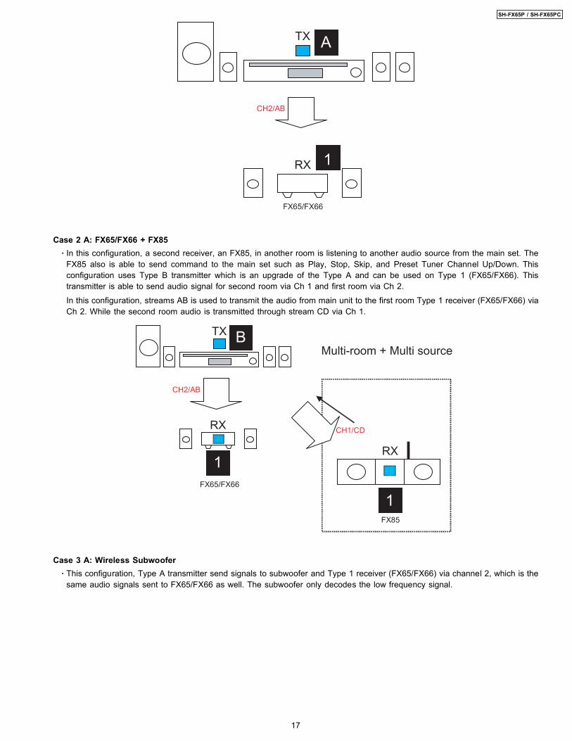
TX
A
1
FX65/FX66
RX
CH2/AB
Case 2 A: FX65/FX66 + FX85 · In this configuration, a second receiver, an FX85, in another room is listening to another audio source from the main set. The
FX85 also is able to send command to the main set such as Play, Stop, Skip, and Preset Tuner Channel Up/Down. Thisconfiguration uses Type B transmitter which is an upgrade of the Type A and can be used on Type 1 (FX65/FX66). Thistransmitter is able to send audio signal for second room via Ch 1 and first room via Ch 2.
In this configuration, streams AB is used to transmit the audio from main unit to the first room Type 1 receiver (FX65/FX66) viaCh 2. While the second room audio is transmitted through stream CD via Ch 1.
Multi-room + Multi source
TX
RX
RX
FX65/FX66
FX85
CH1/CD
CH2/AB
B
1
1
Case 3 A: Wireless Subwoofer · This configuration, Type A transmitter send signals to subwoofer and Type 1 receiver (FX65/FX66) via channel 2, which is the
same audio signals sent to FX65/FX66 as well. The subwoofer only decodes the low frequency signal.
17
SH-FX65P / SH-FX65PC
TX
RX
RX
CH2/AB
CH2/AB
A
1
1
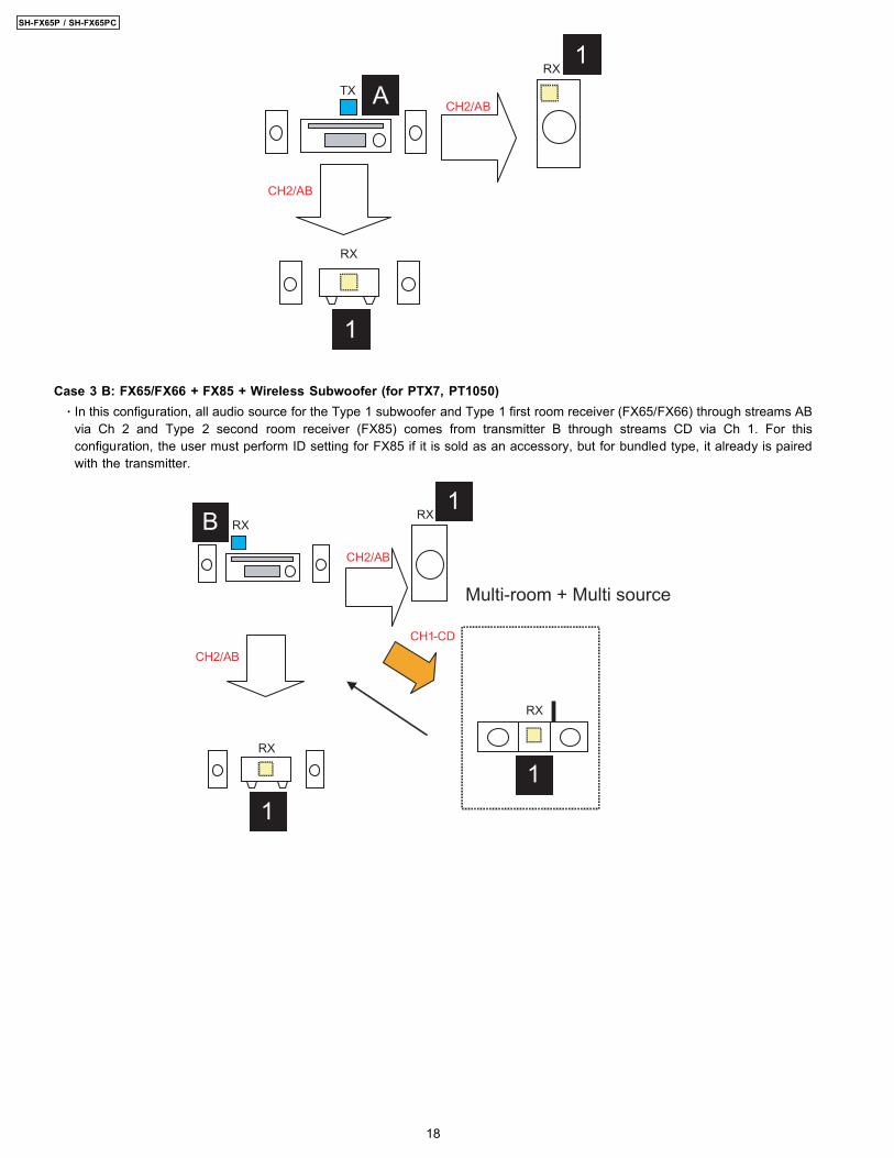
Case 3 B: FX65/FX66 + FX85 + Wireless Subwoofer (for PTX7, PT1050) · In this configuration, all audio source for the Type 1 subwoofer and Type 1 first room receiver (FX65/FX66) through streams AB
via Ch 2 and Type 2 second room receiver (FX85) comes from transmitter B through streams CD via Ch 1. For thisconfiguration, the user must perform ID setting for FX85 if it is sold as an accessory, but for bundled type, it already is pairedwith the transmitter.
RX RX
RX
RX
CH2/AB
CH2/AB
CH1-CD
B 1
1 1
Multi-room + Multi source
18
SH-FX65P / SH-FX65PC
8.1.7. User Operation Flow
START
POWER ON MAINSET
Is Tx card inserted?
Insert Tx card
Is there audio source playing?
Play music
Is music heard on wireless surround
speaker?
Is wireless link led blinking?
Press FF Key in Mainset and 3 keyon remocon until "P" led displays
Press ID set button on receiver
Is wireless link led blinking?
Is wireless receiver on?
Power on receiver
Y
Y
DONE
Y Y
TX-RX probably not paired. Do ID settingprocess
Y
A
Repeat ID set process
A
CHECK FOR SPEAKER WIRE CONNECTIONS
N
N
N
N
8.1.8. Baseband Settings Update from EEPROM IC · The software will read from an external EEPROM IC to get the selected baseband IC settings. Not all baseband register
settings (a total of 512 bytes) will be read from the EEPROM IC, though. Aside from getting the baseband settings from theEEPROM IC, it is also used to enable FCC testing, select the application type and entering into doctor mode (this can beenabled also by sending a command via the main unit).
8.1.9. Doctor Mode · For normal operation but automatic frequency selection is disabled, it can enter into Doctor Mode. This feature is hidden from
normal user and will be used by the service center to fix to a particular RF Channel. With doctor mode, the user can disablefrequency automatic allocation and sniffer and be able to select a fix RF Channel (Channels 1, 2 or 3) by a combination orremote control keys. Refer to Section 9.4 for Wireless Doctor Mode.
19
SH-FX65P / SH-FX65PC
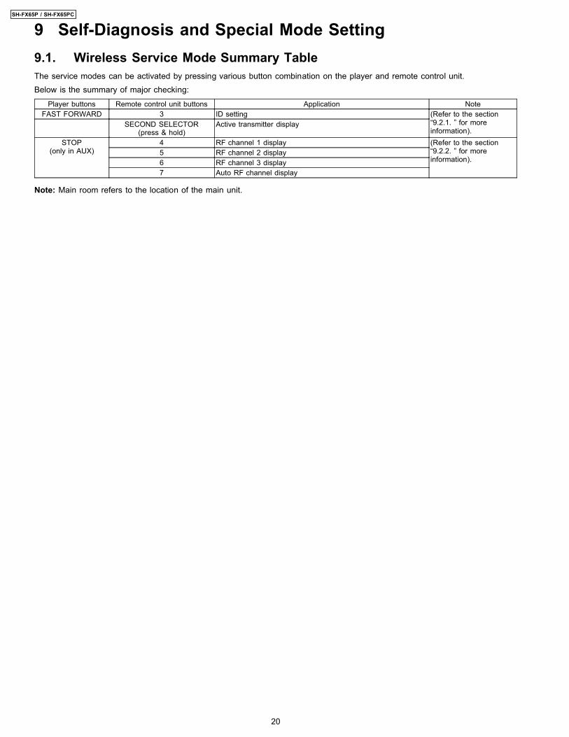
9 Self-Diagnosis and Special Mode Setting9.1. Wireless Service Mode Summary TableThe service modes can be activated by pressing various button combination on the player and remote control unit.Below is the summary of major checking:
Player buttons Remote control unit buttons Application NoteFAST FORWARD 3 ID setting (Refer to the section
“9.2.1. ” for moreinformation).
SECOND SELECTOR(press & hold)
Active transmitter display
STOP(only in AUX)
4 RF channel 1 display (Refer to the section“9.2.2. ” for moreinformation).
5 RF channel 2 display6 RF channel 3 display7 Auto RF channel display
Note: Main room refers to the location of the main unit.
20
SH-FX65P / SH-FX65PC
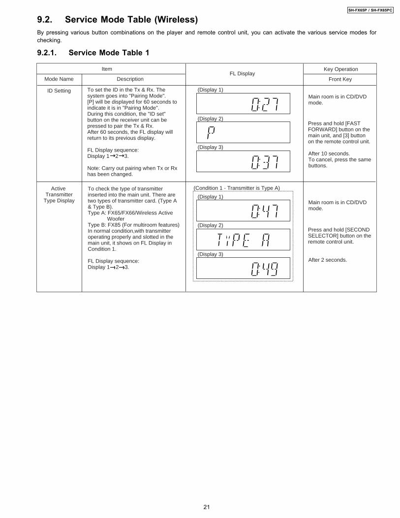
9.2. Service Mode Table (Wireless)By pressing various button combinations on the player and remote control unit, you can activate the various service modes forchecking.
9.2.1. Service Mode Table 1
FL DisplayKey Operation
Front Key
Item
DescriptionMode Name
ID Setting
After 10 seconds.
Active Transmitter
Type Display
To cancel, press the samebuttons.
(Display 1)
(Display 1)
(Condition 1 - Transmitter is Type A)
(Display 2)
(Display 3)
(Display 2)
(Display 3)
After 2 seconds.
Main room is in CD/DVD mode.
Main room is in CD/DVDmode.
Press and hold [FAST FORWARD] button on the main unit, and [3] button on the remote control unit.
Press and hold [SECOND SELECTOR] button on the remote control unit.
To set the ID in the Tx & Rx. The system goes into "Pairing Mode".[P] will be displayed for 60 seconds to indicate it is in "Pairing Mode".During this condition, the "ID set" button on the receiver unit can be pressed to pair the Tx & Rx.After 60 seconds, the FL display willreturn to its previous display.
FL Display sequence:Display 1 2 3.
Note: Carry out pairing when Tx or Rxhas been changed.
To check the type of transmitter inserted into the main unit. There are two types of transmitter card. (Type A & Type B).Type A: FX65/FX66/Wireless Active WooferType B: FX85 (For multiroom features)In normal condition,with transmitteroperating properly and slotted in the main unit, it shows on FL Display in Condition 1.
FL Display sequence:Display 1 2 3.
21
SH-FX65P / SH-FX65PC
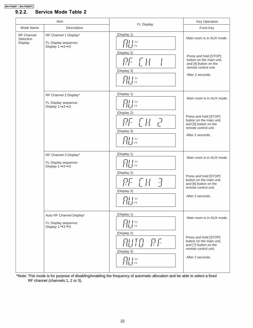
9.2.2. Service Mode Table 2
FL DisplayKey Operation
Front Key
Item
DescriptionMode Name
RF ChannelSelectionDisplay
RF Channel 1 Display*
FL Display sequence:Display 1 2 3
RF Channel 2 Display*
FL Display sequence:Display 1 2 3
Auto RF Channel Display*
FL Display sequence:Display 1 2 3
*Note: This mode is for purpose of disabling/enabling the frequency of automatic*Note: This mode is for purpose of disabling/enabling the frequency of automatic allocation and be able to select a fixed allocation and be able to select a fixed RF channel (channels 1, 2 or 3). RF channel (channels 1, 2 or 3).
After 2 seconds.
(Display 1)
(Display 2)
(Display 3)
After 2 seconds.
Main room is in AUX mode.
Main room is in AUX mode.
Main room is in AUX mode.
Main room is in AUX mode.
Press and hold [STOP] button on the main unit, and [4] button on the remote control unit.
Press and hold [STOP] button on the main unit, and [5] button on the remote control unit.
After 2 seconds.
Press and hold [STOP] button on the main unit, and [6] button on the remote control unit.
After 2 seconds.
Press and hold [STOP] button on the main unit, and [7] button on the remote control unit.
(Display 2)
(Display 1)
(Display 3)
(Display 2)
(Display 1)
(Display 3)
(Display 2)
(Display 1)
(Display 3)
RF Channel 3 Display*
FL Display sequence:Display 1 2 3
22
SH-FX65P / SH-FX65PC
10 Assembling and Disassembling10.1. Note“ATTENTION SERVICER”
Some chassis components may be have sharp edges. Be careful when disassembling and servicing.
1. This section describes procedures for checking the operation of the major printed circuit boards and replacing the maincomponents.
2. For reassembly after operation checks or replacement, reverse the respective procedures.Special reassembly procedures are described only when required.
3. Select items from the following index when checks or replacement are required.
Below is the list of disassembly sections · Disassembly of Top Panel · Disassembly of Led and Led Drive P.C.B · Disassembly of SMPS Module Unit · Disassembly of DAMP P.C.B · Disassembly of Digital Amp IC · Disassembly of Receiver Module P.C.B · Disassembly of Transmitter Module P.C.B (SH-FX65T)
10.1.1. SMPS Module Unit Replacement 1. This model uses SMPS Module unit to provide the necessary supply voltages for the receiver unit (SE-FX65). 2. It is advisable to replace the SMPS Module Unit if upon detecting of non-working conditions. Do not attempt to repair or replace
its components on board.
23
SH-FX65P / SH-FX65PC
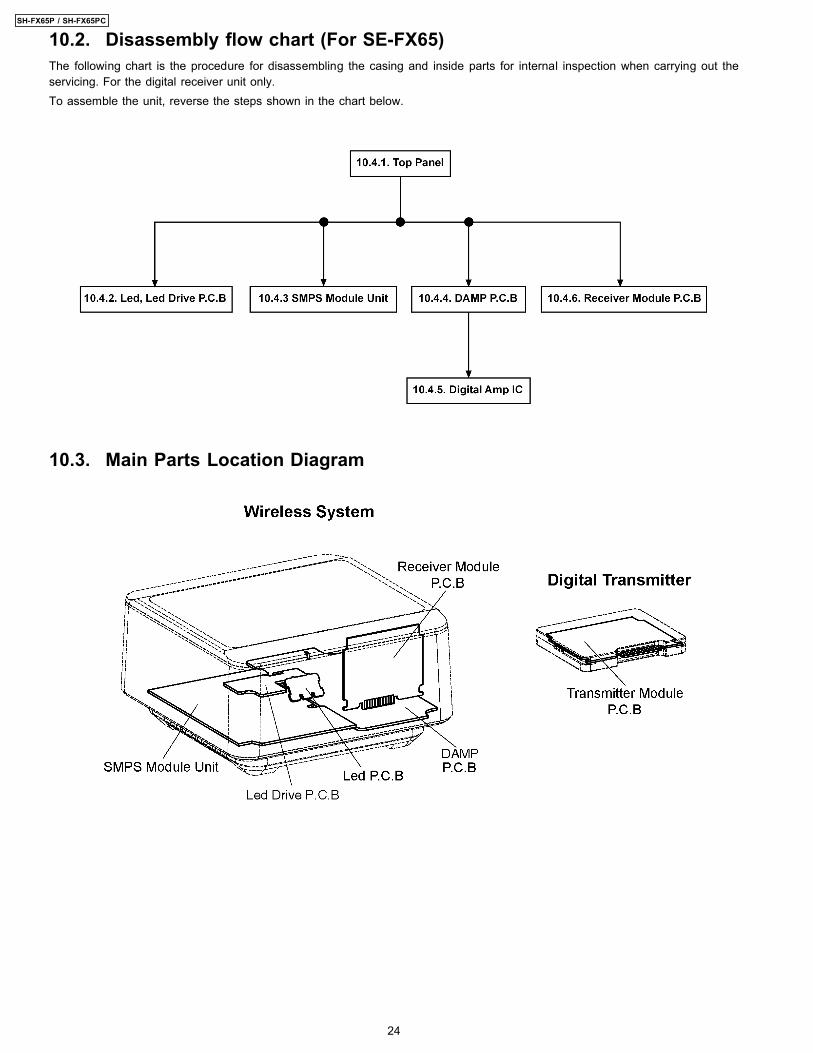
10.2. Disassembly flow chart (For SE-FX65)The following chart is the procedure for disassembling the casing and inside parts for internal inspection when carrying out theservicing. For the digital receiver unit only.To assemble the unit, reverse the steps shown in the chart below.
10.3. Main Parts Location Diagram
24
SH-FX65P / SH-FX65PC
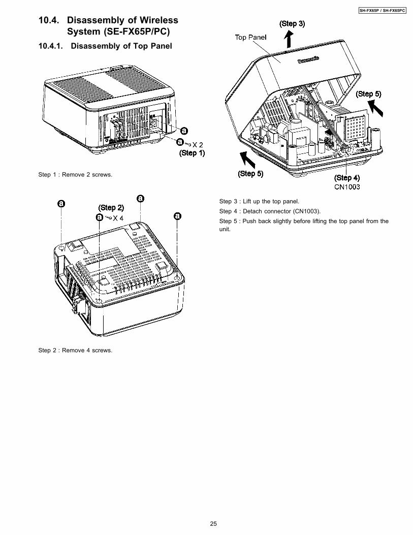
10.4. Disassembly of WirelessSystem (SE-FX65P/PC)
10.4.1. Disassembly of Top Panel
Step 1 : Remove 2 screws.
Step 2 : Remove 4 screws.
Step 3 : Lift up the top panel.Step 4 : Detach connector (CN1003).Step 5 : Push back slightly before lifting the top panel from theunit.
25
SH-FX65P / SH-FX65PC
10.4.2. Disassembly of Led P.C.B and LedDrive P.C.B
· Follow the (Step 1) - (Step 5) of item 10.4.1.
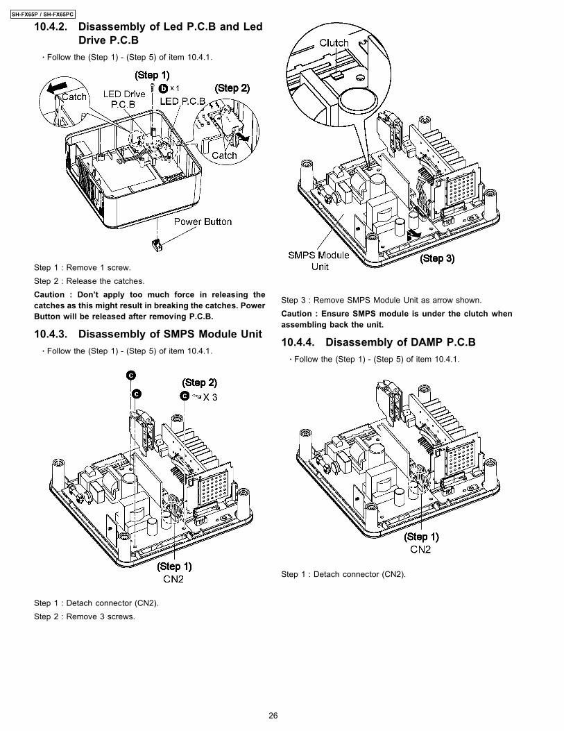
Step 1 : Remove 1 screw.Step 2 : Release the catches.Caution : Don’t apply too much force in releasing thecatches as this might result in breaking the catches. PowerButton will be released after removing P.C.B.
10.4.3. Disassembly of SMPS Module Unit · Follow the (Step 1) - (Step 5) of item 10.4.1.
Step 1 : Detach connector (CN2).Step 2 : Remove 3 screws.
Step 3 : Remove SMPS Module Unit as arrow shown.Caution : Ensure SMPS module is under the clutch whenassembling back the unit.
10.4.4. Disassembly of DAMP P.C.B · Follow the (Step 1) - (Step 5) of item 10.4.1.
Step 1 : Detach connector (CN2).
26
SH-FX65P / SH-FX65PC
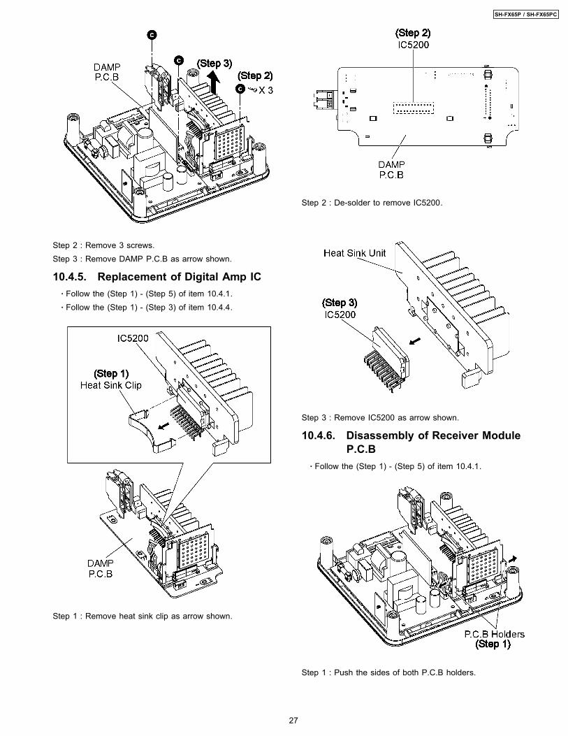
Step 2 : Remove 3 screws.Step 3 : Remove DAMP P.C.B as arrow shown.
10.4.5. Replacement of Digital Amp IC · Follow the (Step 1) - (Step 5) of item 10.4.1. · Follow the (Step 1) - (Step 3) of item 10.4.4.
Step 1 : Remove heat sink clip as arrow shown.
Step 2 : De-solder to remove IC5200.
Step 3 : Remove IC5200 as arrow shown.
10.4.6. Disassembly of Receiver ModuleP.C.B
· Follow the (Step 1) - (Step 5) of item 10.4.1.
Step 1 : Push the sides of both P.C.B holders.
27
SH-FX65P / SH-FX65PC
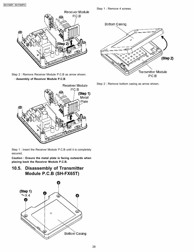
Step 2 : Remove Receiver Module P.C.B as arrow shown. · Assembly of Receiver Module P.C.B
Step 1 : Insert the Receiver Module P.C.B until it is completelysecured.Caution : Ensure the metal plate is facing outwards whenplacing back the Receiver Module P.C.B.
10.5. Disassembly of TransmitterModule P.C.B (SH-FX65T)
Step 1 : Remove 4 screws.
Step 2 : Remove bottom casing as arrow shown.
28
SH-FX65P / SH-FX65PC
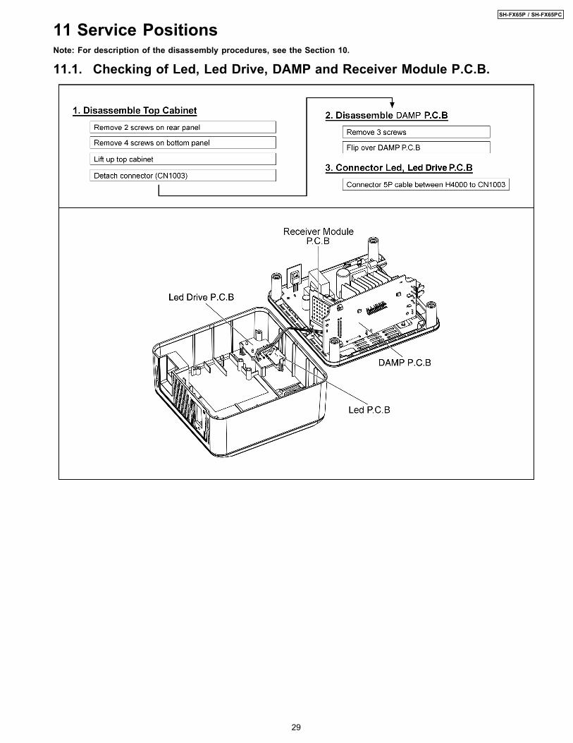
11 Service PositionsNote: For description of the disassembly procedures, see the Section 10.
11.1. Checking of Led, Led Drive, DAMP and Receiver Module P.C.B.
29
SH-FX65P / SH-FX65PC
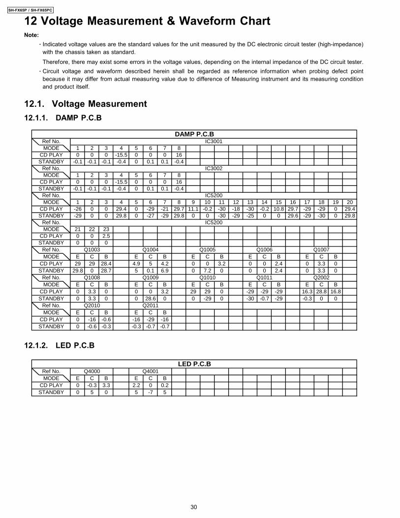
12 Voltage Measurement & Waveform ChartNote:
· Indicated voltage values are the standard values for the unit measured by the DC electronic circuit tester (high-impedance)with the chassis taken as standard.
Therefore, there may exist some errors in the voltage values, depending on the internal impedance of the DC circuit tester. · Circuit voltage and waveform described herein shall be regarded as reference information when probing defect point
because it may differ from actual measuring value due to difference of Measuring instrument and its measuring conditionand product itself.
12.1. Voltage Measurement12.1.1. DAMP P.C.B
Ref No.MODE 1 2 3 4 5 6 7 8
CD PLAY 0 0 0 -15.5 0 0 0 16STANDBY -0.1 -0.1 -0.1 -0.4 0 0.1 0.1 -0.4
Ref No.MODE 1 2 3 4 5 6 7 8
CD PLAY 0 0 0 -15.5 0 0 0 16STANDBY -0.1 -0.1 -0.1 -0.4 0 0.1 0.1 -0.4
Ref No.MODE 1 2 3 4 5 6 7 8 9 10 11 12 13 14 15 16 17 18 19 20
CD PLAY -26 0 0 29.4 0 -29 -21 29.7 11.1 -0.2 -30 -18 -30 -0.2 10.8 29.7 -29 -29 0 29.4STANDBY -29 0 0 29.8 0 -27 -29 29.8 0 0 -30 -29 -25 0 0 29.6 -29 -30 0 29.8
Ref No.MODE 21 22 23
CD PLAY 0 0 2.5STANDBY 0 0 0
Ref No.MODE E C B E C B E C B E C B E C B
CD PLAY 29 29 28.4 4.9 5 4.2 0 0 3.2 0 0 2.4 0 3.3 0STANDBY 29.8 0 28.7 5 0.1 6.9 0 7.2 0 0 0 2.4 0 3.3 0
Ref No.MODE E C B E C B E C B E C B E C B
CD PLAY 0 3.3 0 0 0 3.2 29 29 0 -29 -29 -29 16.3 28.8 16.8STANDBY 0 3.3 0 0 28.6 0 0 -29 0 -30 -0.7 -29 -0.3 0 0
Ref No.MODE E C B E C B
CD PLAY 0 -16 -0.6 -16 -29 -16STANDBY 0 -0.6 -0.3 -0.3 -0.7 -0.7
DAMP P.C.BIC3001
IC3002
IC5200
IC5200
Q1003 Q1004 Q1005 Q1006 Q1007
Q2002
Q2010 Q2011
Q1008 Q1009 Q1010 Q1011
12.1.2. LED P.C.B
Ref No.MODE E C B E C B
CD PLAY 0 -0.3 3.3 2.2 0 0.2STANDBY 0 5 0 5 -7 5
LED P.C.BQ4000 Q4001
30
SH-FX65P / SH-FX65PC
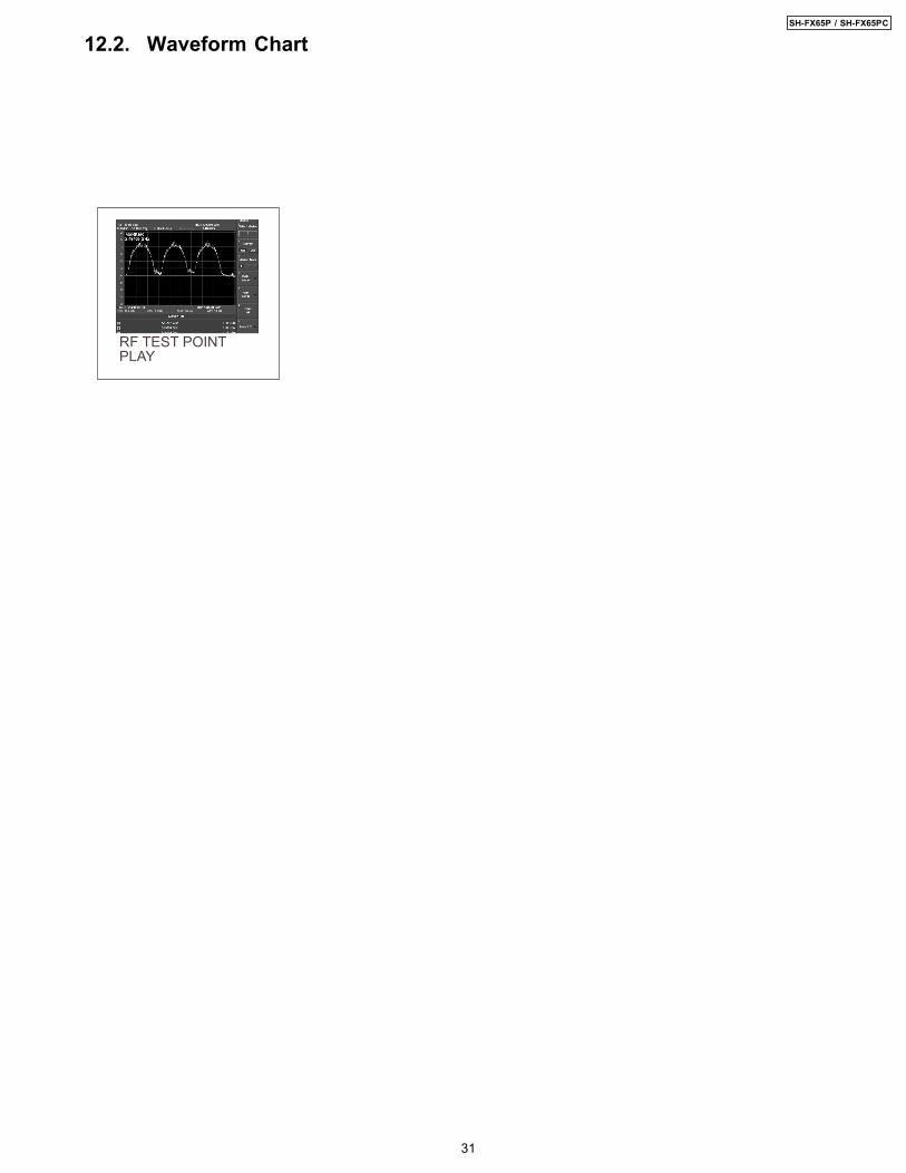
12.2. Waveform Chart
31
SH-FX65P / SH-FX65PC
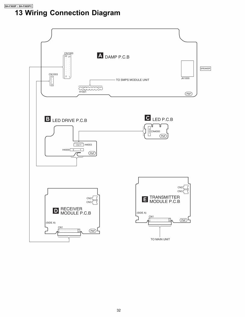
13 Wiring Connection Diagram
32
SH-FX65P / SH-FX65PC
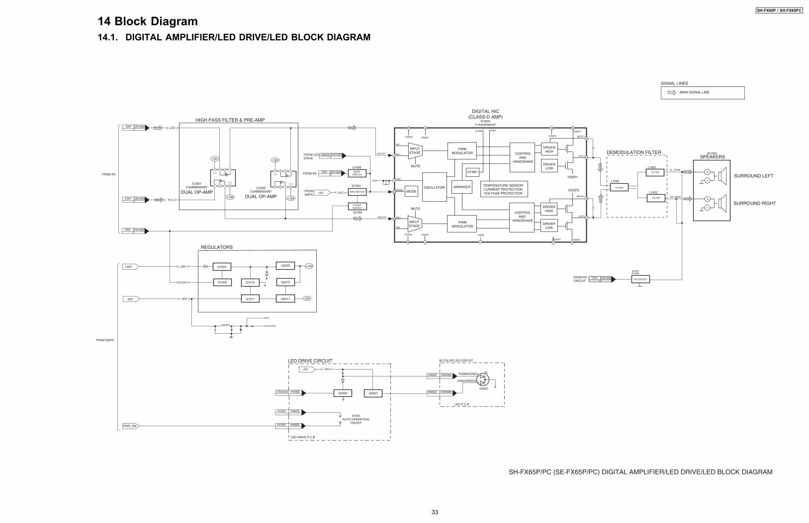
14 Block Diagram14.1. DIGITAL AMPLIFIER/LED DRIVE/LED BLOCK DIAGRAM
+VCC
-VCC
+VCC
-VCC
SH-FX65P / SH-FX65PC
33

14.2. RECEIVER MODULE BLOCK DIAGRAMSH-FX65P / SH-FX65PC
34
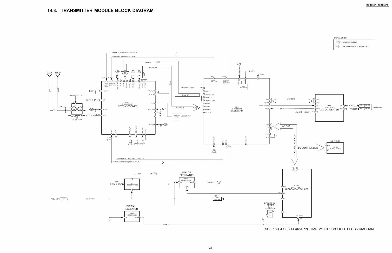
14.3. TRANSMITTER MODULE BLOCK DIAGRAMSH-FX65P / SH-FX65PC
35

SH-FX65P / SH-FX65PC
36
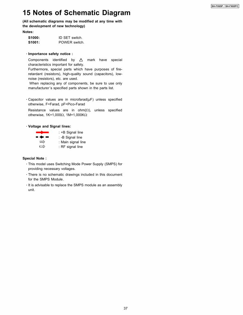
(All schematic diagrams may be modified at any time withthe development of new technology)Notes:
S1000: ID SET switch.S1001: POWER switch.
· Importance safety notice :Components identified by mark have specialcharacteristics important for safety.Furthermore, special parts which have purposes of fire-retardant (resistors), high-quality sound (capacitors), low-noise (resistors), etc. are used.When replacing any of components, be sure to use onlymanufacturer´s specified parts shown in the parts list.
· Capacitor values are in microfarad(µF) unless specifiedotherwise, F=Farad, pF=Pico-FaradResistance values are in ohm(Ω), unless specifiedotherwise, 1K=1,000Ω, 1M=1,000KΩ
· Voltage and Signal lines:: +B Signal line: -B Signal line: Main signal line: RF signal line
Special Note : · This model uses Switching Mode Power Supply (SMPS) for
providing necessary voltages. · There is no schematic drawings included in this document
for the SMPS Module. · It is advisable to replace the SMPS module as an assembly
unit.
15 Notes of Schematic Diagram
37
SH-FX65P / SH-FX65PC

38
SH-FX65P / SH-FX65PC
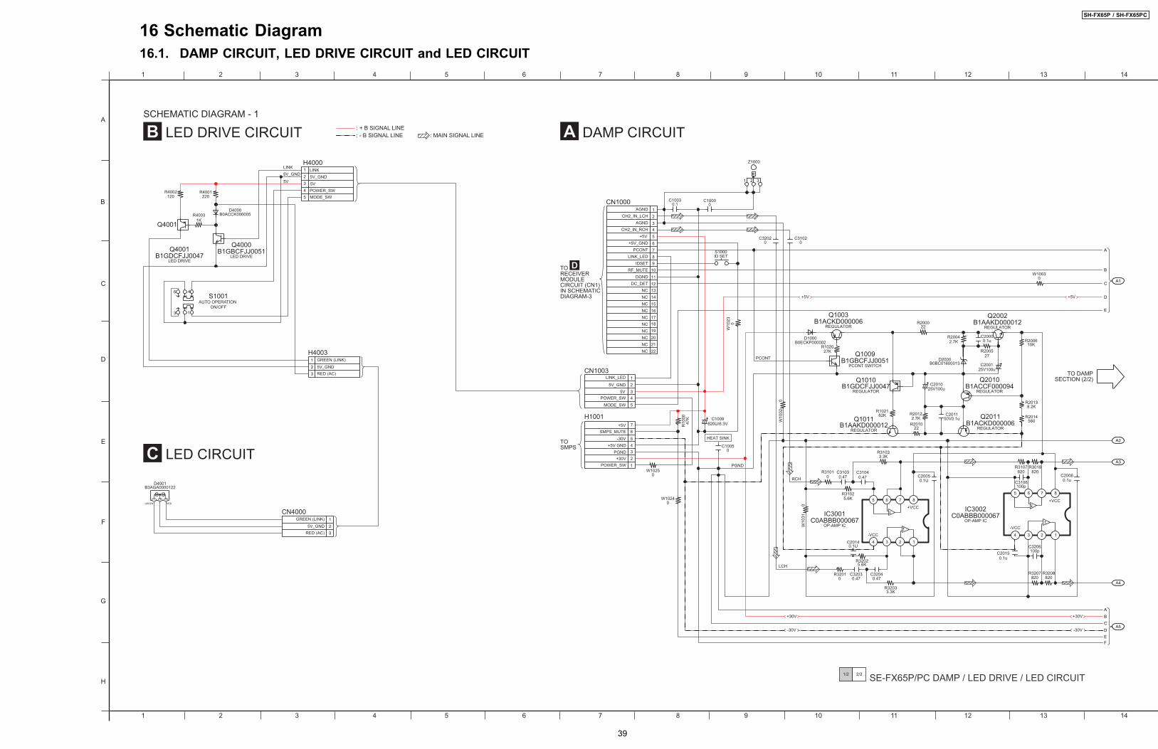
16 Schematic Diagram16.1. DAMP CIRCUIT, LED DRIVE CIRCUIT and LED CIRCUIT
A1
A2
A3
A4
A
B
C
D
E
A5
ABCDEF
321
Z1000
S1000ID SET
C32020
C31020
820U/6.3V
HEAT SINK
C1009
0.47C3204
R32025.6K
0.1UC2014
3.3KR3203
C200125V100u
Q2011B1ACKD000006
REGULATOR
R20122.7K
B1AAKD000012REGULATOR
Q101122
R2010
Q2010B1ACCF000094
REGULATOR
C201150V0.1u
B1GDCFJJ0047REGULATOR
Q1010
Q1009B1GBCFJJ0051
PCONT SWITCH
PGND
C201025V100u
82KR1021
0R3201 C3203
0.47
R2014560
R20138.2K
0.47C3104
R31025.6K
3.3KR3103
0.1UC2005
6 75
24 3
8
1
IC3001C0ABBB000067
OP-AMP IC
IC3002C0ABBB000067
OP-AMP IC
D2000B0BC01600013
C20000.1uD1000
B0ECKP000002
C10050
Q1003B1ACKD000006
REGULATOR 22R2000
2.7KR2004
R200610K
27R2005
0R3101
0.47C3103
Q2002B1AAKD000012
REGULATOR
R102027K
W10
230
W10
02
0
W10
31
0
C3206100p
R3207820
R3208820
C20150.1u
R3107820
R3018820
C20060.1u
6 75
24 3
8
1
C3106100p
23
1
54
CN1003
65
89
1112
10
18
15
1716
2019
1314
7
21
43
2221
CN1000
R10
0047
K
0.1C1003 C1000
0
45
1
32
76
H1001
PCONT
+VCC
-VCC
+5V GNDPGND
5V
NC
NCNC
NCNC
NCNC
NCNC
NC
+5V
5V_GND
LINK_LED
MODE_SWPOWER_SW
SMPS_MUTE
DGNDRF_MUTE
AGND
+5V+5V_GND
AGND
IDSET
PCONTLINK_LED
CH2_IN_LCH
CH2_IN_RCH
DC_DET
-30V
POWER_SW+30V
RCH
+VCC
-VCC
LCH
+5V+5V
+30V+30V
-30V
W10250
W10240
W10030
-30V
D4000B0ACCK000005
R4001220
Q4001
Q4001B1GDCFJJ0047
LED DRIVE
R40031K
R4002120
6
3
4
1
S1001AUTO OPERATION
ON/OFF
Q4000B1GBCFJJ0051
LED DRIVE
23
1
54
H4000
5V
LINK5V_GND
5V5V_GND
POWER_SWMODE_SW
LINK
1
32
H4003
5V_GND
GREEN (LINK)
RED (AC)
1
32
CN4000
5V_GND
GREEN (LINK)
RED (AC)
31 2
D4001B3AGA0000122
REDGREEN
A
B
C
D
E
F
G
H
1 2 3 4 5 6 7 8 9 10 11 12 13 14
1 2 3 4 5 6 7 8 9 10 11 12 13 14
SE-FX65P/PC DAMP / LED DRIVE / LED CIRCUIT1/2 2/2
LED DRIVE CIRCUIT DAMP CIRCUITSCHEMATIC DIAGRAM - 1
: + B SIGNAL LINE: - B SIGNAL LINE : MAIN SIGNAL LINE
TO DAMPSECTION (2/2)
TORECEIVERMODULECIRCUIT (CN1)IN SCHEMATICDIAGRAM-3
TOSMPS
LED CIRCUIT
SH-FX65P / SH-FX65PC
39
A2
A3
A4
A5
ABCDEF
A1
A
B
C
D
E
R10071.2K
R5200
10
C52080.1u
C52100.1u
0R3110
0.47uC5223 R5206
5.6K
330pC5224
R101533K
C10120.1u
R52055.6K
220p
C5211
C5212
220p
C52090.1u
C55230.1u
R5210 10
C55220.1u
C524063V47p
C52220.47u
10R5211
R31130
R31140
C10010
C101135V470P
J0JKB0000020L1004
C10070.1u
R10021.2K
321
K4CZ01000027Z1001
J0JKB0000020L1003
C100435V470P
R10011.2K
C10020.1u
1000pC5221
VSSP
0.1uC5213
0.1uC5207
VDDA2VDDP
VSSA2
R52
085.
6K
C52330.47U
C560216V10U
C52
320.
47U
1000pC5231
C52200.1u
C52140.1u
R52
075.
6K Q1008B1ABCF000176
DC DETECT
Q1007B1ABCF000176
DC DETECTQ1007
0.1uC5219
C12190.1u
321
Z1002
C10060
21
43
JK1000
SPEAKERS
C11
190.
1uC11180.1u
C12
180.
1u
5.6KR1208
2
43
1
G0B9R5K00003L1002
R32100
R120722
C12170.1u
C12160.68u
2
43
1
L1000G0A150L00003
R101122K
R1013120K
6.3V100uC1014
0R3214
0R3213
C52341000p
R11085.6K
C11170.1u
22R1107 R1014
120K
2
43
1
G0B9R5K00003L1001
C11160.68u
R52041.5K
C52150.1u
R5201
10C52
060.
1u
220p
C5218
220p
C5205
0.1uC5217C5200
0.1u
220p
C5203
C5204
0.015u
4.7KR1010
Q1006B1GBCFJJ0051
MUTE SWITCH
Q1005B1GBCFJJ0051
PCONT SWITCH
Q1004B1ADCE000012
BIAS SWITCH
R10094.7K
Q1005
R10081.2K
C5216330pC5201
0.015u
19 21 2322201021 8 9743 5 6 12 1514 17 18161311
IC5200C1BA00000487
DIGITAL HIC (CLASS-D AMP)
C52
020.
22u
RCH
LCH
LCH
RCH
AGNDAGND
HEAT SINK
SURROND RIGHTSURROND LEFT
OU
T1
VS
SD
OU
T2
OS
C
IN1+
IN1-
PR
OT
BO
OT2
VD
DP
2
VS
SP
1
STA
BI
VS
SA
1
VD
DA
1
SG
ND
1
BO
OT1
VD
DP
1
VS
SP
2
VD
DA
2
MO
DE
IN2-
IN2+
VS
SA
2
SG
ND
2
+30V
+30V
+5V
-30V
15 16 17 18 19 20 21 22 23 24 25 26 27 28
15 16 17 18 19 20 21 22 23 24 25 26 27 28
A
B
D
E
F
H
G
C
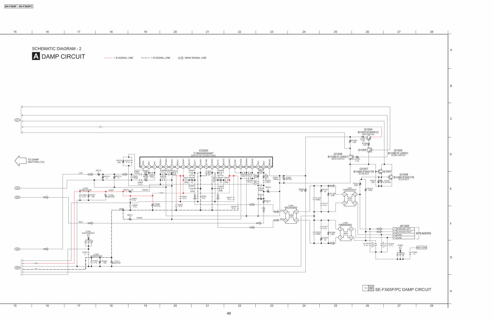
SE-FX65P/PC DAMP CIRCUIT1/2 2/2
DAMP CIRCUITSCHEMATIC DIAGRAM - 2
TO DAMPSECTION (1/2)
: + B SIGNAL LINE : + B SIGNAL LINE : MAIN SIGNAL LINE
SH-FX65P / SH-FX65PC
40
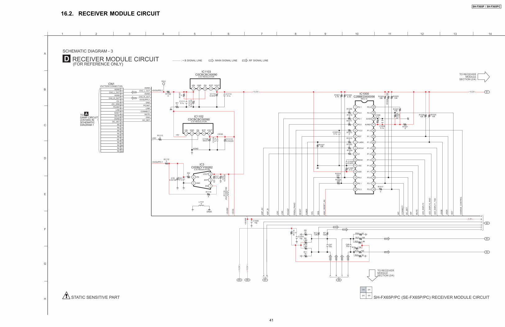
16.2. RECEIVER MODULE CIRCUIT
B1
B3
B2
B4
A
BCDEF
B5 B6 B7
A B
B8
A B C D
C11136.3V47
C11140.1u 4.7K
R1001 10K
R10
04
10KR1005
10KR1007
10KR10034.7K
R1002
421 3 5
IC1103C0CBCBC00090
3.3V REGULATOR
AGND
0R1024
0R1023
0R1013C1110
6.3V220
+3V3A
C70.1u
330R1022
R101.8K
R81.8K
R111K
R91K
R11
15 0
C150310p
R710K
C4733p
R1310K
+3V
3RF
C150610p
R11
19J0
JCC
0000
166
+3V
3RF
R27 10K
R26 1K
C4833p R19 1.8K
R22 1K
R18 10K
R25 1.8K
INT
AS
IC_R
ES
ET_
(N)
0
R1017
CO
NN
EC
T
SD
A
C10054.7u
R1014330
0.047uC1004
10KR1027
DC
_DE
T
SC
L
+3V
3A
FLM
D0
JOG
B
JOG
A
WP
MU
TE
LED
_DS
PLY
3
RE
SE
T
LED
_DS
PLY
2_R
XD
LED
_DS
PLY
1_TX
D
AS
P_S
I
AS
P_S
C
C70
6.3V
220
C110816V4.7
GNDE
L11010
R1116
0
2
4
1
3
5
IC3C0DBZYY00262
3.3V REGULATOR
0R1021
0R1011
C10010.1u 0
R1012
R10
062.
2K
C10090.1u
10KR1026
10KR1025
0R1009
C10084.7u0
R1010
C11
090.
1u
KE
Y
CH
AR
GE
_CO
NTR
OL
PW
DA
_PW
AD
PC
ON
T
LIN
K
LDO
13
14
12
9
11
10
2
3
4
1
7
8
6
5
17
19
21
23
26
25
29
28
30
27
24
22
20
18
15 16
IC1000C2BBED000056
MCU IC
MUTE
LINKCONNECT
LDO
DC_DETGND
+5V
6.3V
100
C11
12
CH2_L_OUTAGND
AGND
TP21
+5VSUPPLY
CH2_R_OUT+5VSUPPLY
PCONTGND
R11060
0.1uC1111
R11
07 0
421 3 5
IC1102C0CBCBC00090
3.3V REGULATOR
R11120
C196.3V100
+5VSUPPLY
R11130
65
89
1112
10
18
15
1716
2019
1314
7
21
43
2221
CN1(PATTERN CONNECTOR)
C510.1u
P2.3
P2.2
P1.3
P1.4
P1.2
P1.1
P3.0
P1.5
P1.6
P1.7
P1.0
AVSS
P3.1
AVREF
P3.2
BYP
BYP
EN
EN
VOUT
VOUT
VIN
VIN
DC_DET
NC
NC
NCNC
NC
NC
LINK
DGNDMUTEIDSET
GND
GND
BYPEN VOUT
AGND
+5V
CH2_L_OUT
CH2_R_OUT
+5V_GND
VIN
AGND
GND
PCONT
P2.0
P2.1
P12.0
RST
P0.0
P0.1
NCNCNC
NC
P3.3
P6.0
P6.1
FLMD0
VSS
VDD
X1
REGC
EXCLK
+3.3V +3.3V
+3.3
V
+3.3
V
3.3V
W10
W40
A
B
C
D
E
F
G
H
1 2 3 4 5 6 7 8 9 10 11 12 13 14
SCHEMATIC DIAGRAM - 3
SH-FX65P/PC (SE-FX65P/PC) RECEIVER MODULE CIRCUIT3/4 4/4
1/4 2/4
TO RECEIVERMODULE
SECTION (2/4)
TO RECEIVER MODULESECTION (3/4)
TODAMP CIRCUIT(CN1000) INSCHEMATICDIAGRAM-1
RECEIVER MODULE CIRCUIT (FOR REFERENCE ONLY)
: + B SIGNAL LINE : MAIN SIGNAL LINE : RF SIGNAL LINE
STATIC SENSITIVE PART
SH-FX65P / SH-FX65PC
41
B3
B4
B1
B2
A
BCDEF
B14 B15 B16 B17 B18
A B C D
R14080
R14090
0.1uC1404
10V22uC1403
R14000
0.1uC1406
6.3V10uC1405
TP22
31
2
IC1105C1BB00001071POWER ON RESET IC
TP23
0.047uC1101
R11011K
SD
A
R11050
LR_C
LK
C11030.1u
C11020.047u
SC
L
R11040
WP
R110310K
AU
DIO
CLK
PW
DA
_PW
AD
B_C
LK
+3V
3A
R110210K
6
7
5
2
4
3
81
IC1101EEPROM IC
(NOT SUPPLIED)R
ES
ET
10V22uC1401
10V22uC1402
R140447K
R14021K
R1411
0R1407
0
R14100
SD
_OU
T_B
7
5
6
1
2
4
3
10
9
12
14
15
16
13
11
8
IC1400C0FBBK000066
DAC
R14050
R140347K
CH
2_R
_OU
T
R14011K
CH
2_L_
OU
T
VSS
VDD
D1F1
VCOM
MCLK
PDN
BICK
LRCK
SDTI
TEST
NC
NC
VOUTVIN
VSS
NC
GND
VCC
WP
SCL
SDA
DEM
DFSI
DFS0
D1F0
ROUT
LOUT
+3.3V
3.3V
+3.3
V
15 16 17 18 19 20 21 22 23 24 25 26 27 28
A
B
D
E
F
H
G
C
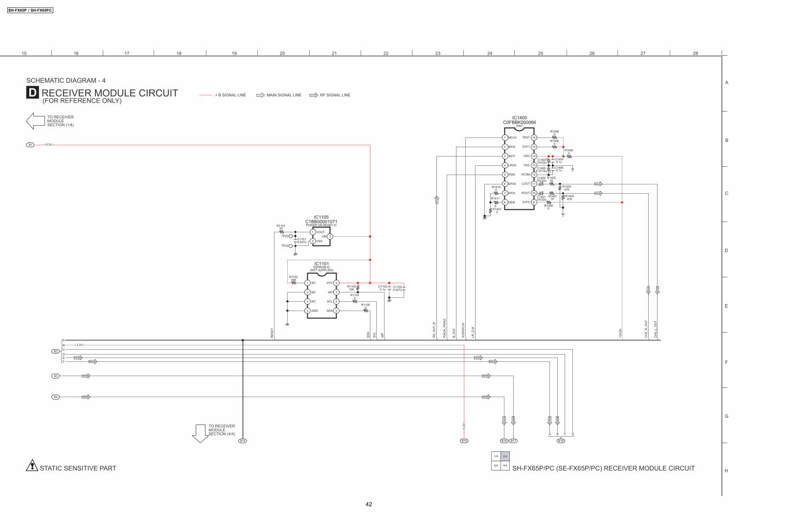
SCHEMATIC DIAGRAM - 4
SH-FX65P/PC (SE-FX65P/PC) RECEIVER MODULE CIRCUIT STATIC SENSITIVE PART 3/4 4/4
1/4 2/4
TO RECEIVER MODULESECTION (1/4)
TO RECEIVER MODULESECTION (4/4)
RECEIVER MODULE CIRCUIT (FOR REFERENCE ONLY)
: + B SIGNAL LINE : MAIN SIGNAL LINE : RF SIGNAL LINE
SH-FX65P / SH-FX65PC
42
B9
B10
A
B
CDE
B11
B12
A
B
C
B13
AB
C
D
E
F
G
H
I
B5 B6 B7
A B
B8
A B C D
C2710p
C3910p
0.56pC83
C751p
1.0pC88
C861.0p
C3210V10u
R430
R210
C1100p
C5
0.1u
C15
05
C15
04
C1509100p
C15080.1u
C67
10p
10p
10p
C8100p
C410.01u
R440
L21G1C4N7ZA0068
L17G1C3N9ZA0068
L20G1C4N7ZA0068
C851.0p
L15F1G1HR56A561
C28100p
C871.0p
0.56pC80
L16G1C3N9ZA0068
C36.3V1100
R380
R390
C150710p
C740.56p
C5910p
C420.01u
C6110p
C6010p
C90.01u
C3833p
C15100.1u
C29100pC310.1u
0.01uC58
32
1 4
Y2
H0J
2205
0000
1
C110.01u
C5733p
R15G1C47NJA0048C46
22pC4947p
R470
R4510
R24 6.8K
C1422p
C154.7p
R282.2KC13680p
C1511100p
C18 0.01u
C12100p
C200.01u
C6210p
R460
45 4447 46 43
1
4
3
5
6
2
48
10
12
11
7
8
9
41 394042
28
3738
31
32
30
36
34
33
35
29
26
25
27
16 1714 15 1813 2420 222119 23
IC13C1CB00002648
RF IC
R6G1C2N7ZA0068
R1G1C2N7ZA0068
RF_TEST_POINT
RF_TEST_POINT
23
1
54
23
1
54
C402.2p
C4315p
9
12
1011
7
654
3
8
2 1IC1
IC1C1CB00001841TRANSFER SWITCH IC
C4510p
C4410p
CN3(PATTERN CONNECTOR)
CN2(PATTERN CONNECTOR)
PCB ANT
PCB ANT
B1
VR
X_B
B_I
+
BYPASS
B4
VCC_CP
XTAL
VCC_VCO
GND_CP
TUNE
GND_VCO
RX_BB_Q+
RX_BB_Q-
CP
_OU
T
VCC_XTAL
GND_XTAL
VR
X_B
B_I
-
RX
TX
ANT1
V1
ANT2
V2
CLO
CK
OU
TR
X_H
P
LDV
CC
_RX
_VG
A
B6
ANT2-
VC
C_T
X_P
A
B5
/CS
B2
B3
B7
ANT1+
/SHDN
VCC_PA
ANT2+
ANT1-
CP
RX
TX
AN
T_S
EL
VC
C_R
X_M
X
VCC_LNA
GND_RX_LNA
TX_B
B_Q
-D
IN
VC
C_P
LLV
CC
_RX
_FL
TX_B
BI+
TX_B
BI-
RS
SI
SC
LK
VC
C_T
X_M
X
TX_B
B_Q
+
+3.3
V
+3.3
V
+3.3V
W30
1 2 3 4 5 6 7 8 9 10 11 12 13 14
I
J
L
M
N
P
O
K
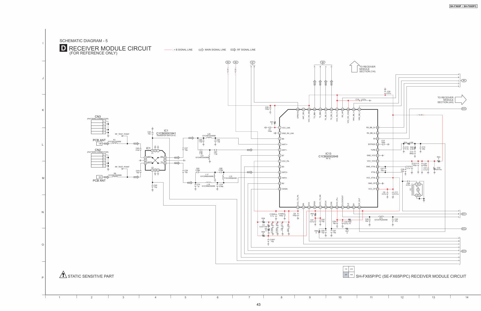
SCHEMATIC DIAGRAM - 5
SH-FX65P/PC (SE-FX65P/PC) RECEIVER MODULE CIRCUIT3/4 4/4
1/4 2/4
TO RECEIVERMODULE
SECTION (4/4)
TO RECEIVER MODULESECTION (1/4)
RECEIVER MODULE CIRCUIT (FOR REFERENCE ONLY)
: + B SIGNAL LINE : MAIN SIGNAL LINE : RF SIGNAL LINE
STATIC SENSITIVE PART
SH-FX65P / SH-FX65PC
43
B10
B12
B13
AB
C
D
E
F
G
H
I
B11
A
B
C
B9
A
B
CDE
B14 B15 B16 B17 B18
A B C D
C1010K
R4110K
0R1507
C26
0.04
7u
R510
33pC66
R4
82K
0.04
7uC
22
0.04
7uC
24
0.04
7uC
23
321
4
Y1H0J12250003733p
C65
C54
10p
C53
10p
R1501 33
R1503 33
R1502 33
R1500 33
C56
10p
R1505 33
J0JCC0000278R1506
R1504 33
C55
10p
C17
10p
C52
10p
SD_OUT_A
SD_IN_B
SD_IN_A
B_CLK
LR_CLK
SD_OUT_B
AUDIOCLK
SDA
SCL
ASIC_RESET_(N)
INT
FRAME_CLK
DEBUG_TXDCONNECT
K4
K5
K6
C360.01u
C300.01u
C340.01u
C330.01u
C370.01u
C210.01u
C256.3V4.7
23
58
45
44
47
48
46
30 31 32
43
40
41
35
37
36
33
34
39
38
42
2825 2624 27 29
5556 5051 495354 52576263 61
1918 20
3
2
5
4
6
8
7
1
64
15
16
9
13
10
12
11
14
17 2221
5960
IC10C1AB00002772
BASE BAND IC
BB
_RX
IPX
TAL_
2
VC
C2_
IOR
EFP
BB
_RX
INX
TAL_
1
VC
M
GP
IO_0
/ C
ON
SDA
A0
AGND_IO
VCC_3_IO
AUDIO_CLK_OUT
A1
GPIO_RESN
SCL
GP
IO_3
/ D
BG
_TX
D
GP
IO_1
/ FR
M_C
LK
GPIO_2 / INT
RS
ET
B4
BB
_RX
QN
BB
_RX
QP
LRCK
DIN_B
BCK
DIN_A
DOUT_B
DOUT_A
VC
C2_
A
GN
D_A
RE
FN
VC
C3A
_AD
CG
ND
_IO
TMO
GN
D_A
GN
D_K
VC
C3A
_RE
G
VCC_K
TX_ANT_A_EN
TX_DATA_I
TX_ANT_C_EN
TX_DATA_I_NOT
B2
SHDN
SPI_EN
SPI_CLK
VCC_3_IO
B5_MODE_PA
TX_ON
GND_IO
B3_AGC_RESET
RX
HP
CLK
_IN
SP
I_D
ATA
CLK
_OU
T
B1_
AG
CS
ET
B6_RX_ANT_B_EN
B6_RX_ANT_A_EN
TX_D
ATA
_Q
TX_D
ATA
_Q_N
OT
V25
GN
D_A
_AD
CV
CC
_K
+3.3V
15 16 17 18 19 20 21 22 23 24 25 26 27 28
I
J
L
M
N
P
O
K
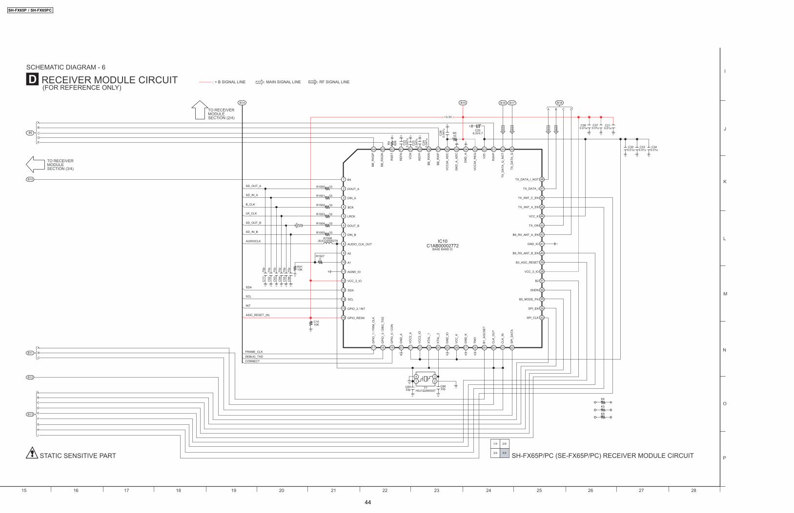
SCHEMATIC DIAGRAM - 6
SH-FX65P/PC (SE-FX65P/PC) RECEIVER MODULE CIRCUIT3/4 4/4
1/4 2/4
TO RECEIVER MODULESECTION (3/4)
TO RECEIVER MODULESECTION (2/4)
RECEIVER MODULE CIRCUIT (FOR REFERENCE ONLY)
: + B SIGNAL LINE : MAIN SIGNAL LINE : RF SIGNAL LINE
STATIC SENSITIVE PART
SH-FX65P / SH-FX65PC
44
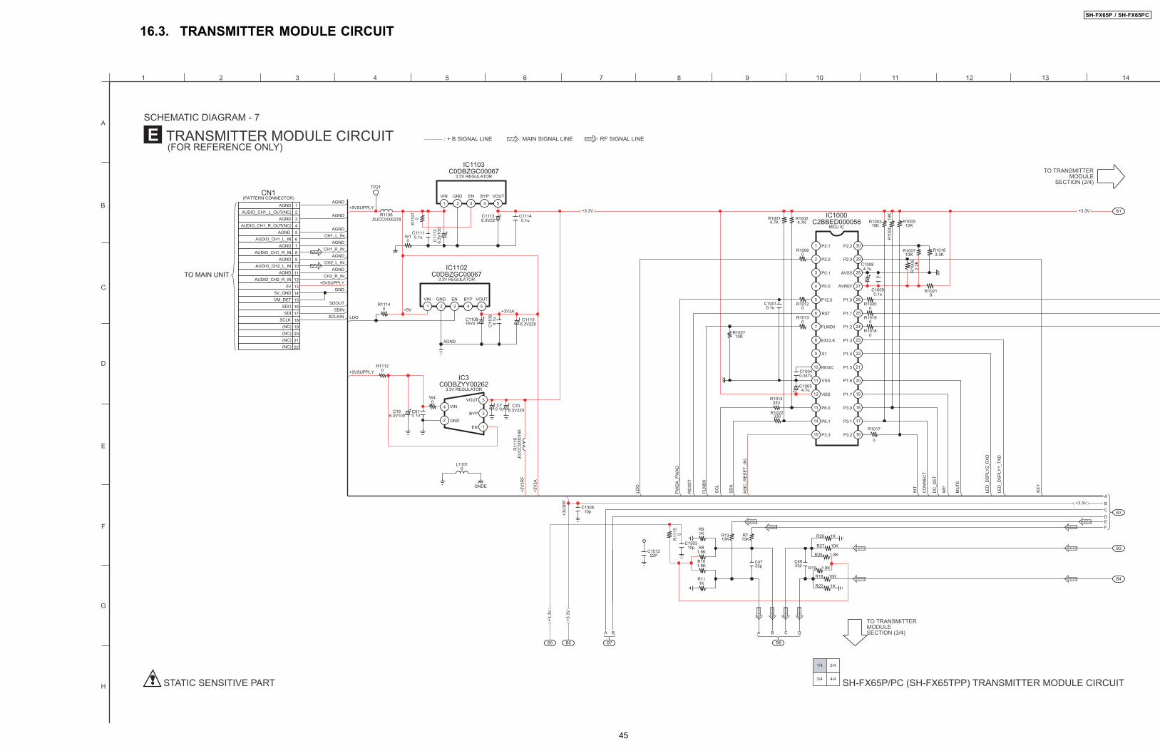
16.3. TRANSMITTER MODULE CIRCUIT
B1
B3
B2
B4
A
BCDEF
B5 B6 B7
A B
B8
A B C D
C11136.3V22
C11140.1u 4.7K
R1001 10K
R10
04
10KR1005
10KR1007 R1016
3.3K
10KR10034.7K
R1002
421 3 5
IC1103C0DBZGC00067
3.3V REGULATOR
AGND
0R1013C1110
6.3V220
+3V3A
C70.1u
330R1022
R101.8K
R81.8K
R111K
R91K
R11
15 0
C150310p
C151222P
R710K
C4733p
R1310K
+3V
3RF
C150610p
R11
19J0
JCC
0000
166
+3V
3RF
R27 10K
R26 1K
C4833p R19 1.8K
R22 1K
R18 10K
R25 1.8K
INT
AS
IC_R
ES
ET_
(N)
0
R1017
CO
NN
EC
T
SD
A
C10054.7u
R1014330
0.047uC1004
10KR1027
DC
_DE
T
SC
L
+3V
3A
FLM
D0
WP
MU
TE
RE
SE
T
LED
_DS
PLY
2_R
XD
LED
_DS
PLY
1_TX
D
C706.3V220
C110816V4.7
GNDE
L11010
2
4
1
3
5
IC3C0DBZYY00262
3.3V REGULATOR
0R1021
R10200
R10190
R10180
C10010.1u 0
R1012
R10
062.
2K
C10090.1u
0R1009
C10084.7u
C11
090.
1u
KE
Y
PW
DA
_PW
AD
LDO
13
14
12
9
11
10
2
3
4
1
7
8
6
5
17
19
21
23
26
25
29
28
30
27
24
22
20
18
15 16
IC1000C2BBED000056
MCU IC
CH2_L_IN
CH1_R_INAGND
LDOSCLKIN
+5VSUPPLYCH2_R_IN
AGND
SDINSDOUT
+5V
6.3V
100
C11
12
AGND
AGND
TP21
+5VSUPPLY
AGND
GND
AGNDCH1_L_IN
R1106J0JCC0000278
0.1uC1111
R11
07 0
421 3 5
IC1102C0DBZGC00067
3.3V REGULATOR
R11120
C196.3V100
+5VSUPPLY
R11140
65
89
1112
10
18
15
1716
2019
1314
7
21
43
2221
C510.1u
P2.3
P2.2
P1.3
P1.4
P1.2
P1.1
P3.0
P1.5
P1.6
P1.7
P1.0
AVSS
P3.1
AVREF
P3.2
BYPEN VOUTVIN
AUDIO_CH2_R_IN
SCLK
SDO
5V_GNDVM_DET
5V
SDI
AUDIO_CH1_R_IN
AGNDAUDIO_CH2_L_IN
AGND
GND
BYPEN VOUT
AGND
AGND
AUDIO_CH1_L_OUT(NC)
AUDIO_CH1_R_OUT(NC)
AUDIO_CH1_L_IN
VIN
AGND
GND
AGND
P2.0
P2.1
P12.0
RST
P0.0
P0.1
(NC)(NC)(NC)
(NC)
P3.3
P6.0
P6.1
FLMD0
VSS
VDD
X1
REGC
EXCLK
+3.3V +3.3V
+3.3
V
+3.3
V
+3.3V
BYP
EN
VOUTVIN
GND
W10
CN1(PATTERN CONNECTOR)
W40
A
B
C
D
E
F
G
H
1 2 3 4 5 6 7 8 9 10 11 12 13 14
SCHEMATIC DIAGRAM - 7
SH-FX65P/PC (SH-FX65TPP) TRANSMITTER MODULE CIRCUIT3/4 4/4
1/4 2/4
TO TRANSMITTERMODULE
SECTION (2/4)
TO TRANSMITTERMODULESECTION (3/4)
TO MAIN UNIT
TRANSMITTER MODULE CIRCUIT (FOR REFERENCE ONLY)
: + B SIGNAL LINE : MAIN SIGNAL LINE : RF SIGNAL LINE
STATIC SENSITIVE PART
SH-FX65P / SH-FX65PC
45
B3
B4
B1
B2
A
BCDEF
B14 B15 B16 B17 B18
A B C D
TP22
31
2
IC1105C1BB00001071POWER ON RESET IC
TP23
0.1C1101
R11011K
SD
A
R11050
SD
_IN
_B
LR_C
LK
C11030.1u
C11020.047u
SC
L
R11040
WP
R110310K
AU
DIO
CLK
PW
DA
_PW
AD
B_C
LK
+3V
3A
R110210K
6
7
5
2
4
3
81
IC1101EEPROM IC
NOT SUPPLIEDR
ES
ET
SD
0
SD
I
CH
2_L_
IN
CH
2_R
_IN
SC
LK
SC
LKIN
SD
IN
C130110V22
C130510V22
R13050
R13060
C13060.1
10V22C1307 C1308
0.1
C130310V22
C130210V22
R13011K
R13021K
R130347K
R13
0447
K
C13040.1
7
5
6
1
2
4
3
10
12
14
15
16
13
11
89
IC1300C0FBAK000019
ADC
DIF
PDN
MCLK
CKS2
SDTO
SCLK
LRCK
CKS0
VCOM
CKS1
VD
VA
AGND
DGND
AINL
AINR
+3.3V +3.3V
+3.3V
+3.3
V
R111147K
R111027K
R110910K
R110810K
SD
OU
T
+5V
SU
PP
LY
Q1101B1GBCFJJ0051
LEVEL SHIFTER
NC
NC
VOUTVIN
VSS
NC
GND
VCC
WP
SCL
SDA
D1102B0JCAE000001
D1101B0JCAE000001
15 16 17 18 19 20 21 22 23 24 25 26 27 28
A
B
D
E
F
H
G
C
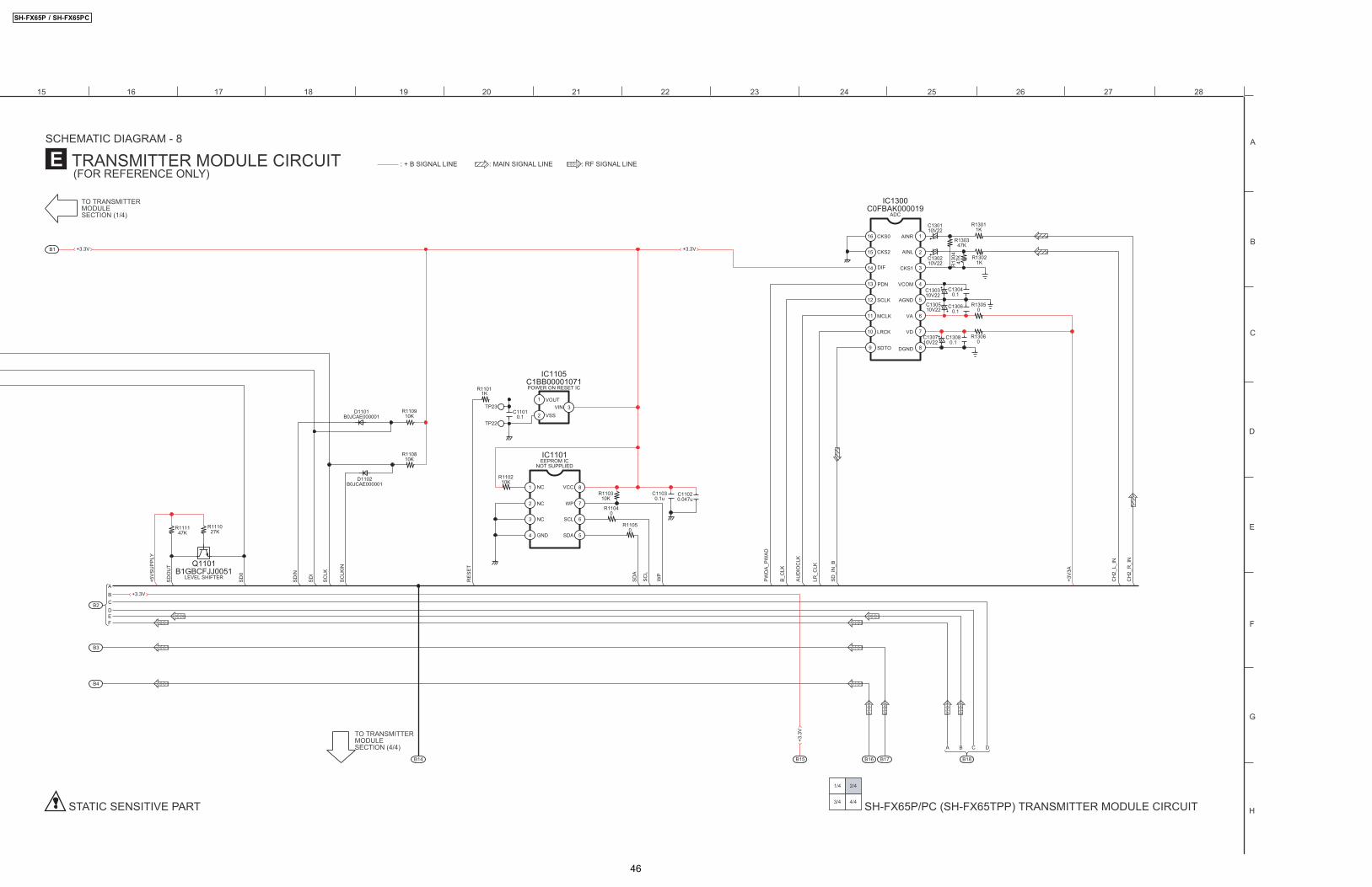
SCHEMATIC DIAGRAM - 8
SH-FX65P/PC (SH-FX65TPP) TRANSMITTER MODULE CIRCUIT3/4 4/4
1/4 2/4
TO TRANSMITTERMODULESECTION (1/4)
TO TRANSMITTERMODULESECTION (4/4)
TRANSMITTER MODULE CIRCUIT (FOR REFERENCE ONLY)
: + B SIGNAL LINE : MAIN SIGNAL LINE : RF SIGNAL LINE
STATIC SENSITIVE PART
SH-FX65P / SH-FX65PC
46
B9
B10
A
B
CDE
B11
B12
A
B
C
B13
AB
C
D
E
F
G
H
I
B5 B6 B7
A B
B8
A B C D
C2710p
C3910p
0.56pC83
C751p
1.0pC88
C861.0p
C3210V10
R430
R210
C1100p
C5
0.1u
C15
05
C15
04
C1509100p
C15080.1u
C67
10p
10p
10p
C8100p
C151322p
C410.01u
R440
L21G1C4N7ZA0068
L17G1C3N9ZA0068
L20G1C4N7ZA0068
C851.0p
L15F1G1HR56A561
C28100p
C871.0p
0.56pC80
L16G1C3N9ZA0068
C36.3V100
R380
R390
C150710p
C740.56p
C5910p
C420.01u
C6110p
C6010p
C90.01u
C3833p
C15100.1u
C29100pC310.1u
0.01uC58
32
1 4
Y2
H0J
2205
0000
1
C110.01u
C5733p
R15G1C47NJA0048C46
22pC4947p
R470
R4510
R24 6.8K
C1422p
C154.7p
R282.2KC13680p
C1511100p
C18 0.01u
C12100p
C200.01u
C6210p
R460
45 4447 46 43
1
4
3
5
6
2
48
10
12
11
7
8
9
41 394042
28
3738
31
32
30
36
34
33
35
29
26
25
27
16 1714 15 1813 2420 222119 23
IC13C1CB00002648
RF IC
R6G1C2N7ZA0068
R1G1C2N7ZA0068
23
1
54
23
1
54
C402.2p
C4315p
9
12
1011
7
654
3
8
2 1IC1
IC1C1CB00001841
TRANSMITTER SWITCH IC
C4510p
C4410p
B1
VR
X_B
B_I
+
BYPASS
B4
VCC_CP
XTAL
VCC_VCO
GND_CP
TUNE
GND_VCO
RX_BB_Q+
RX_BB_Q-
CP
_OU
T
VCC_XTAL
GND_XTAL
VR
X_B
B_I
-
RX
TX
ANT1
V1
ANT2
V2
CLO
CK
OU
TR
X_H
P
LDV
CC
_RX
_VG
A
B6
ANT2-
VC
C_T
X_P
A
B5
/CS
B2
B3
B7
ANT1+
/SHDN
VCC_PA
ANT2+
ANT1-
CP
RX
TX
AN
T_S
EL
VC
C_R
X_M
X
VCC_LNA
GND_RX_LNA
TX_B
B_Q
-D
IN
VC
C_P
LLV
CC
_RX
_FL
TX_B
BI+
TX_B
BI-
RS
SI
SC
LK
VC
C_T
X_M
X
TX_B
B_Q
+
+3.3
V
+3.3
V
+3.3V
PCB ANT
PCB ANT
RF_TEST_POINT
RF_TEST_POINT
W30
CN3(PATTERN CONNECTOR)
CN2(PATTERN CONNECTOR)
1 2 3 4 5 6 7 8 9 10 11 12 13 14
I
J
L
M
N
P
O
K
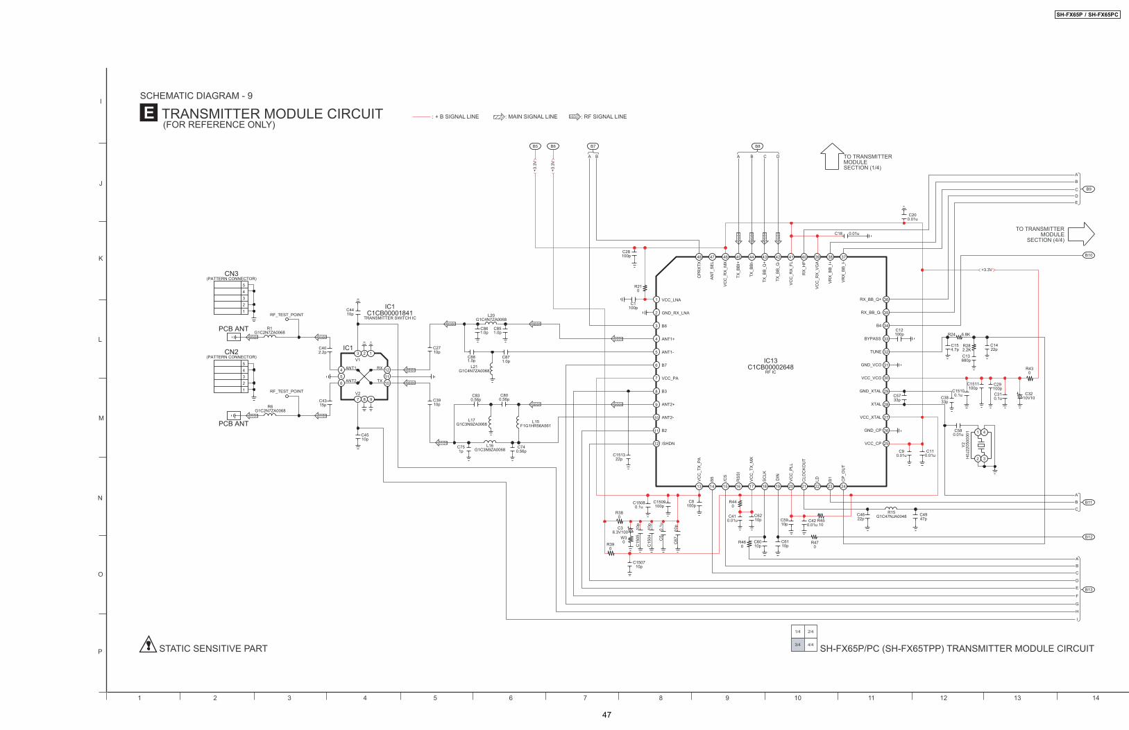
SCHEMATIC DIAGRAM - 9
SH-FX65P/PC (SH-FX65TPP) TRANSMITTER MODULE CIRCUIT3/4 4/4
1/4 2/4
TO TRANSMITTERMODULE
SECTION (4/4)
TO TRANSMITTERMODULESECTION (1/4)
TRANSMITTER MODULE CIRCUIT (FOR REFERENCE ONLY)
: + B SIGNAL LINE : MAIN SIGNAL LINE : RF SIGNAL LINE
STATIC SENSITIVE PART
SH-FX65P / SH-FX65PC
47
B10
B12
B13
AB
C
D
E
F
G
H
I
B11
A
B
C
B9
A
B
CDE
B14 B15 B16 B17 B18
A B C D
C1010K
R4110K
0R1507
C26
0.04
7u
R510
33pC66
R4
82K
0.04
7uC
22
0.04
7uC
24
0.04
7uC
23
321
4
Y1H0J12250003733p
C65
C54
10p
C53
10p
R1501 33
R1503 33
R1502 33
R1500 33
C56
10p
R1505 33
J0JCC0000278R1506
R1504 33
C55
10p
C17
10p
C52
10p
SD_OUT_A
SD_IN_B
SD_IN_A
B_CLK
LR_CLK
SD_OUT_B
AUDIOCLK
SDA
SCL
ASIC_RESET_(N)
INT
FRAME_CLK
DEBUG_TXDCONNECT
C360.01u
C300.01u
C340.01u
C330.01u
C370.01u
C210.01u
C256.3V4.7
23
58
45
44
47
48
46
30 31 32
43
40
41
35
37
36
33
34
39
38
42
2825 2624 27 29
5556 5051 495354 52576263 61
1918 20
3
2
5
4
6
8
7
1
64
15
16
9
13
10
12
11
14
17 2221
5960
IC10C1AB00002772
BASE BAND IC
BB
_RX
IPX
TAL_
2
VC
C2_
IOR
EFP
BB
_RX
INX
TAL_
1
VC
M
GP
IO_0
/ C
ON
SDA
A0
AGND_IO
VCC_3_IO
AUDIO_CLK_OUT
A1_TM_SEL0
GPIO_RESN
SCL
GP
IO_3
/ D
BG
_TX
D
GP
IO_1
/ FR
M_C
LK
GPIO_2 / INT
RS
ET
B4
BB
_RX
QN
BB
_RX
QP
LRCK
DIN_B
BCK
DIN_A
DOUT_B
DOUT_A
VC
C2_
A
GN
D_A
RE
FN
VC
C3A
_AD
CG
ND
_IO
TMO
GN
D_A
GN
D_K
VC
C3A
_RE
G
VCC_K
TX_ANT_A_EN
TX_DATA_I
TX_ANT_C_EN
TX_DATA_I_NOT
B2
SHDN
SPI_EN
SPI_CLK
VCC_3_IO
B5_MODE_PA
TX_ON
GND_IO
B3_AGC_RESET
RX
HP
CLK
_IN
SP
I_D
ATA
CLK
_OU
T
B1_
AG
CS
ET
B6_RX_ANT_B_EN
B6_RX_ANT_A_EN
TX_D
ATA
_Q
TX_D
ATA
_Q_N
OT
V25
GN
D_A
_AD
CV
CC
_K
+3.3V
15 16 17 18 19 20 21 22 23 24 25 26 27 28
I
J
L
M
N
P
O
K
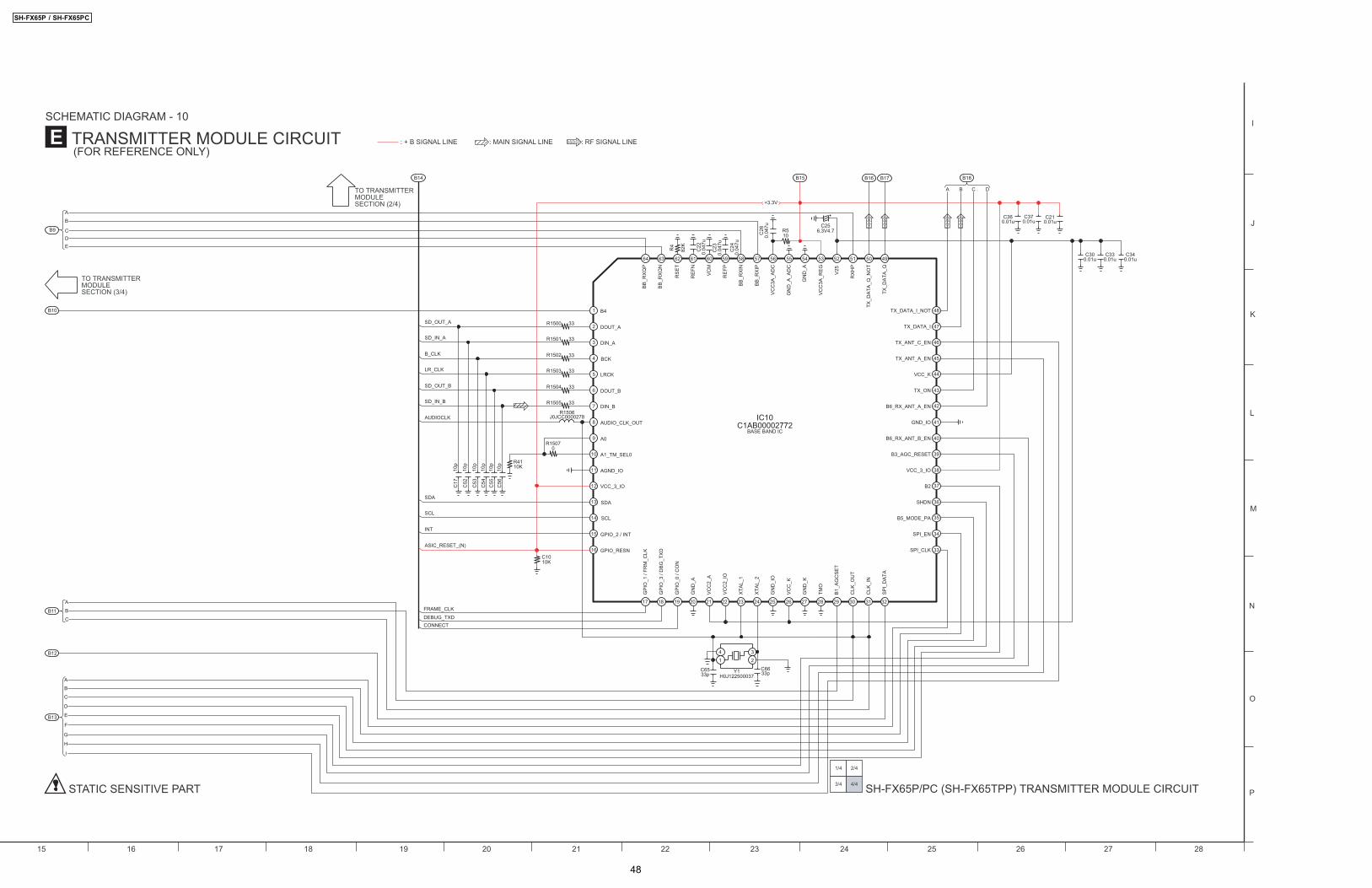
SCHEMATIC DIAGRAM - 10
SH-FX65P/PC (SH-FX65TPP) TRANSMITTER MODULE CIRCUIT3/4 4/4
1/4 2/4
TO TRANSMITTERMODULESECTION (3/4)
TO TRANSMITTERMODULESECTION (2/4)
TRANSMITTER MODULE CIRCUIT (FOR REFERENCE ONLY)
: + B SIGNAL LINE : MAIN SIGNAL LINE : RF SIGNAL LINE
STATIC SENSITIVE PART
SH-FX65P / SH-FX65PC
48
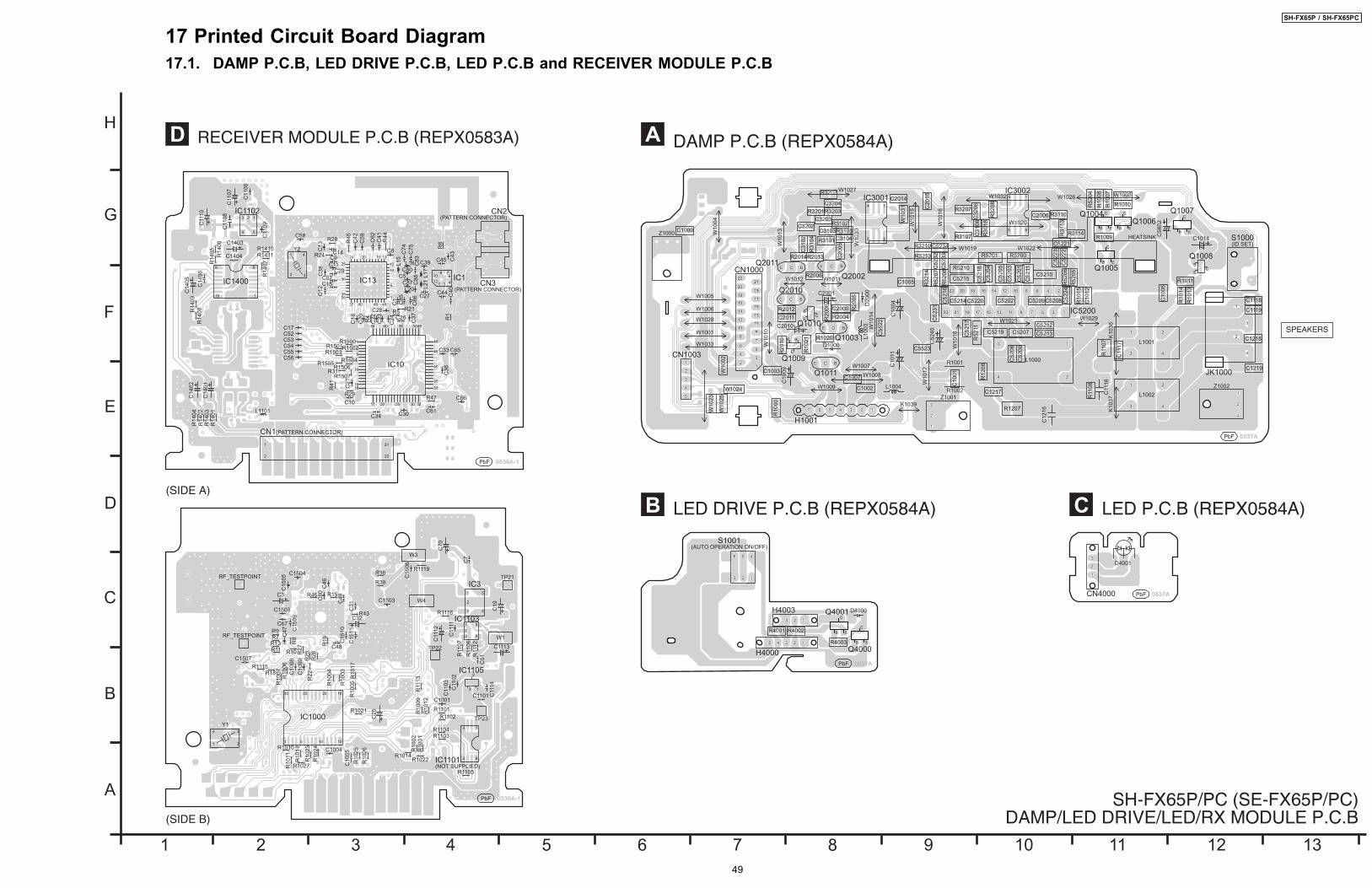
17 Printed Circuit Board Diagram17.1. DAMP P.C.B, LED DRIVE P.C.B, LED P.C.B and RECEIVER MODULE P.C.B
!
!
"
"
#
$
$
%
%
%
$
$
$
&'
$
$
'
'
'
$
$
$
$
$
$
$
!
'
SH-FX65P / SH-FX65PC
49
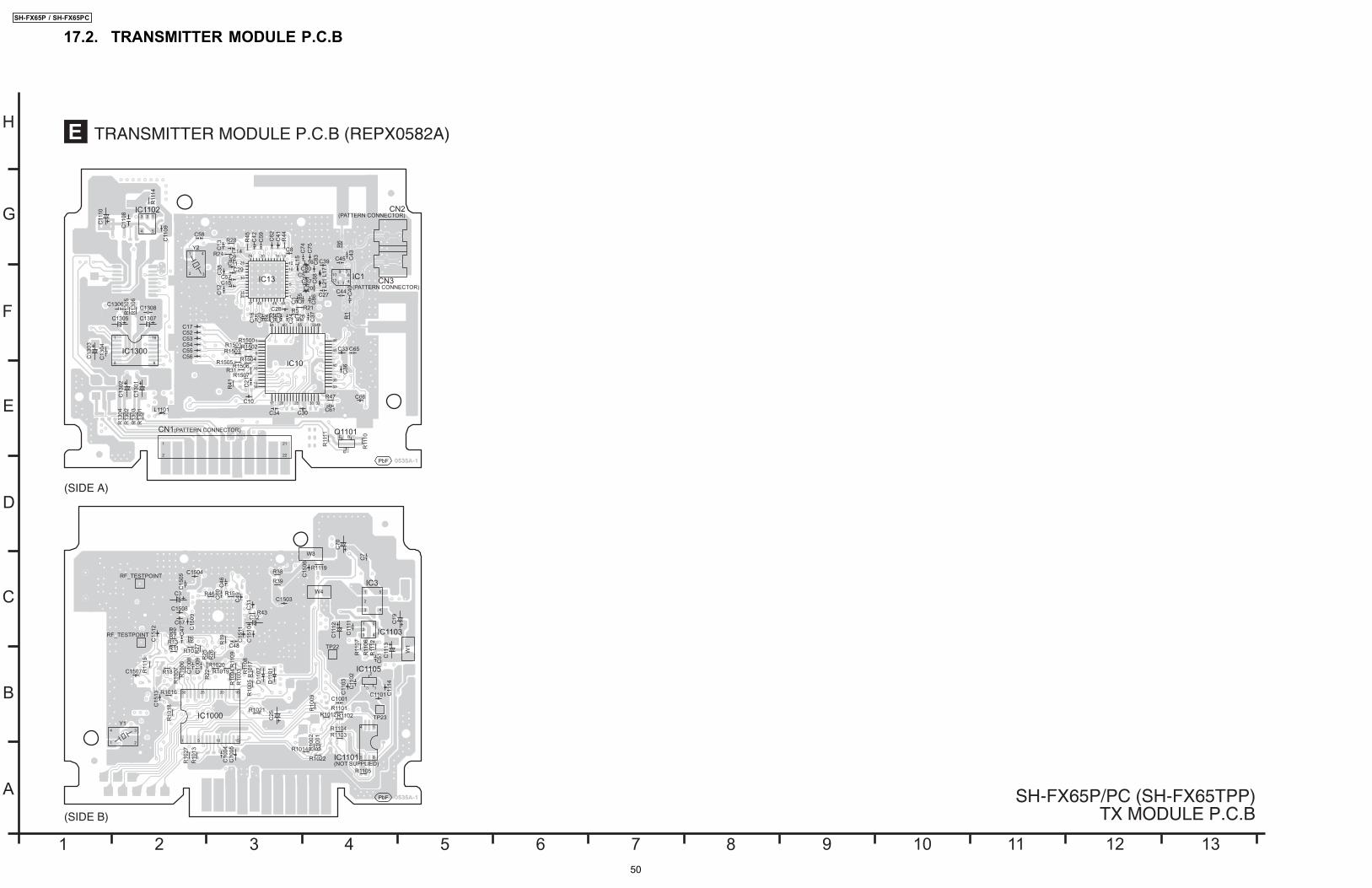
17.2. TRANSMITTER MODULE P.C.B
""
"#""
$
!
!
"
"
SH-FX65P / SH-FX65PC
50
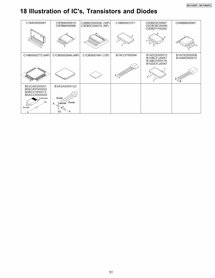
18 Illustration of IC's, Transistors and Diodes
51
SH-FX65P / SH-FX65PC
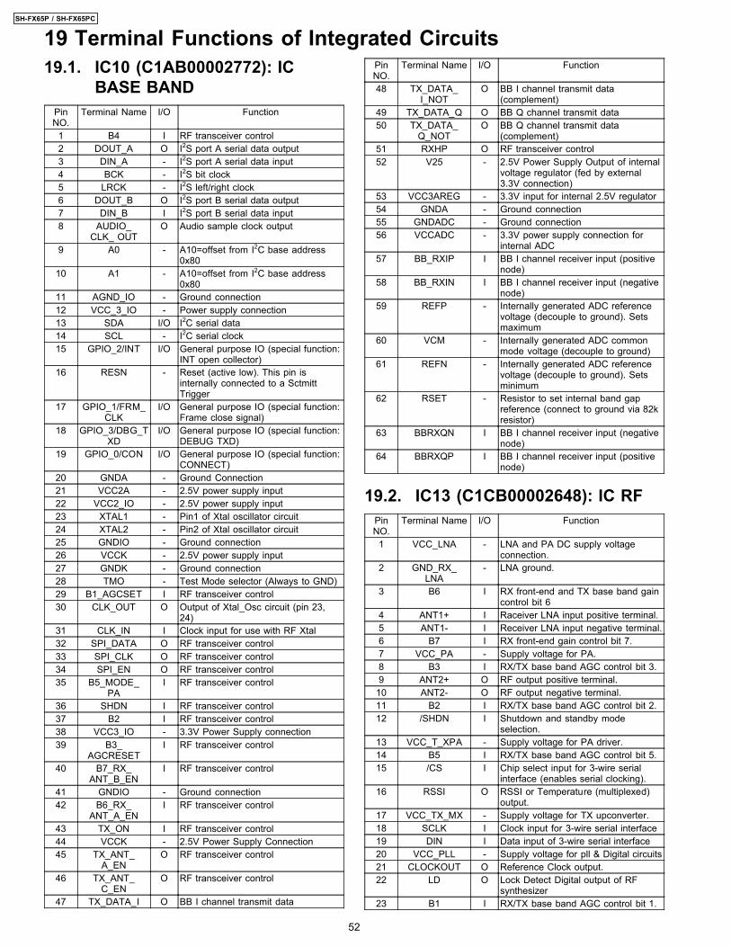
19.1. IC10 (C1AB00002772): ICBASE BAND
PinNO.
Terminal Name I/O Function
1 B4 I RF transceiver control2 DOUT_A O I2S port A serial data output3 DIN_A - I2S port A serial data input4 BCK - I2S bit clock5 LRCK - I2S left/right clock6 DOUT_B O I2S port B serial data output7 DIN_B I I2S port B serial data input8 AUDIO_
CLK_ OUTO Audio sample clock output
9 A0 - A10=offset from I2C base address0x80
10 A1 - A10=offset from I2C base address0x80
11 AGND_IO - Ground connection12 VCC_3_IO - Power supply connection13 SDA I/O I2C serial data14 SCL - I2C serial clock15 GPIO_2/INT I/O General purpose IO (special function:
INT open collector)16 RESN - Reset (active low). This pin is
internally connected to a SctmittTrigger
17 GPIO_1/FRM_CLK
I/O General purpose IO (special function:Frame close signal)
18 GPIO_3/DBG_TXD
I/O General purpose IO (special function:DEBUG TXD)
19 GPIO_0/CON I/O General purpose IO (special function:CONNECT)
20 GNDA - Ground Connection21 VCC2A - 2.5V power supply input22 VCC2_IO - 2.5V power supply input23 XTAL1 - Pin1 of Xtal oscillator circuit24 XTAL2 - Pin2 of Xtal oscillator circuit25 GNDIO - Ground connection26 VCCK - 2.5V power supply input27 GNDK - Ground connection28 TMO - Test Mode selector (Always to GND)29 B1_AGCSET I RF transceiver control30 CLK_OUT O Output of Xtal_Osc circuit (pin 23,
24)31 CLK_IN I Clock input for use with RF Xtal32 SPI_DATA O RF transceiver control33 SPI_CLK O RF transceiver control34 SPI_EN O RF transceiver control35 B5_MODE_
PAI RF transceiver control
36 SHDN I RF transceiver control37 B2 I RF transceiver control38 VCC3_IO - 3.3V Power Supply connection39 B3_
AGCRESETI RF transceiver control
40 B7_RX_ANT_B_EN
I RF transceiver control
41 GNDIO - Ground connection42 B6_RX_
ANT_A_ENI RF transceiver control
43 TX_ON I RF transceiver control44 VCCK - 2.5V Power Supply Connection45 TX_ANT_
A_ENO RF transceiver control
46 TX_ANT_C_EN
O RF transceiver control
47 TX_DATA_I O BB I channel transmit data
PinNO.
Terminal Name I/O Function
48 TX_DATA_I_NOT
O BB I channel transmit data(complement)
49 TX_DATA_Q O BB Q channel transmit data50 TX_DATA_
Q_NOTO BB Q channel transmit data
(complement)51 RXHP O RF transceiver control52 V25 - 2.5V Power Supply Output of internal
voltage regulator (fed by external3.3V connection)
53 VCC3AREG - 3.3V input for internal 2.5V regulator54 GNDA - Ground connection55 GNDADC - Ground connection56 VCCADC - 3.3V power supply connection for
internal ADC57 BB_RXIP I BB I channel receiver input (positive
node)58 BB_RXIN I BB I channel receiver input (negative
node)59 REFP - Internally generated ADC reference
voltage (decouple to ground). Setsmaximum
60 VCM - Internally generated ADC commonmode voltage (decouple to ground)
61 REFN - Internally generated ADC referencevoltage (decouple to ground). Setsminimum
62 RSET - Resistor to set internal band gapreference (connect to ground via 82kresistor)
63 BBRXQN I BB I channel receiver input (negativenode)
64 BBRXQP I BB I channel receiver input (positivenode)
19.2. IC13 (C1CB00002648): IC RFPinNO.
Terminal Name I/O Function
1 VCC_LNA - LNA and PA DC supply voltageconnection.
2 GND_RX_LNA
- LNA ground.
3 B6 I RX front-end and TX base band gaincontrol bit 6
4 ANT1+ I Raceiver LNA input positive terminal.5 ANT1- I Receiver LNA input negative terminal.6 B7 I RX front-end gain control bit 7.7 VCC_PA - Supply voltage for PA.8 B3 I RX/TX base band AGC control bit 3.9 ANT2+ O RF output positive terminal.10 ANT2- O RF output negative terminal.11 B2 I RX/TX base band AGC control bit 2.12 /SHDN I Shutdown and standby mode
selection.13 VCC_T_XPA - Supply voltage for PA driver.14 B5 I RX/TX base band AGC control bit 5.15 /CS I Chip select input for 3-wire serial
interface (enables serial clocking).16 RSSI O RSSI or Temperature (multiplexed)
output.17 VCC_TX_MX - Supply voltage for TX upconverter.18 SCLK I Clock input for 3-wire serial interface19 DIN I Data input of 3-wire serial interface20 VCC_PLL - Supply voltage for pll & Digital circuits21 CLOCKOUT O Reference Clock output.22 LD O Lock Detect Digital output of RF
synthesizer23 B1 I RX/TX base band AGC control bit 1.
19 Terminal Functions of Integrated Circuits
52
SH-FX65P / SH-FX65PC
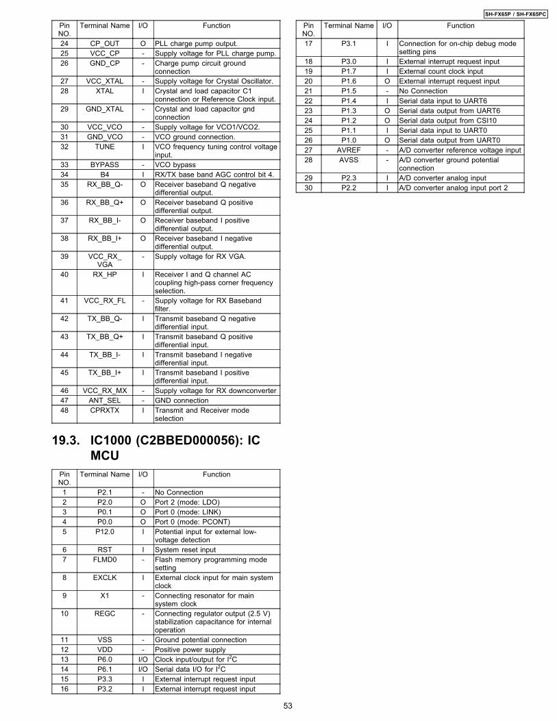
PinNO.
Terminal Name I/O Function
24 CP_OUT O PLL charge pump output.25 VCC_CP - Supply voltage for PLL charge pump.26 GND_CP - Charge pump circuit ground
connection27 VCC_XTAL - Supply voltage for Crystal Oscillator.28 XTAL I Crystal and load capacitor C1
connection or Reference Clock input.29 GND_XTAL - Crystal and load capacitor gnd
connection30 VCC_VCO - Supply voltage for VCO1/VCO2.31 GND_VCO - VCO ground connection.32 TUNE I VCO frequency tuning control voltage
input.33 BYPASS - VCO bypass34 B4 I RX/TX base band AGC control bit 4.35 RX_BB_Q- O Receiver baseband Q negative
differential output.36 RX_BB_Q+ O Receiver baseband Q positive
differential output.37 RX_BB_I- O Receiver baseband I positive
differential output.38 RX_BB_I+ O Receiver baseband I negative
differential output.39 VCC_RX_
VGA- Supply voltage for RX VGA.
40 RX_HP I Receiver I and Q channel ACcoupling high-pass corner frequencyselection.
41 VCC_RX_FL - Supply voltage for RX Basebandfilter.
42 TX_BB_Q- I Transmit baseband Q negativedifferential input.
43 TX_BB_Q+ I Transmit baseband Q positivedifferential input.
44 TX_BB_I- I Transmit baseband I negativedifferential input.
45 TX_BB_I+ I Transmit baseband I positivedifferential input.
46 VCC_RX_MX - Supply voltage for RX downconverter47 ANT_SEL - GND connection48 CPRXTX I Transmit and Receiver mode
selection
19.3. IC1000 (C2BBED000056): ICMCU
PinNO.
Terminal Name I/O Function
1 P2.1 - No Connection2 P2.0 O Port 2 (mode: LDO)3 P0.1 O Port 0 (mode: LINK)4 P0.0 O Port 0 (mode: PCONT)5 P12.0 I Potential input for external low-
voltage detection6 RST I System reset input7 FLMD0 - Flash memory programming mode
setting8 EXCLK I External clock input for main system
clock9 X1 - Connecting resonator for main
system clock10 REGC - Connecting regulator output (2.5 V)
stabilization capacitance for internaloperation
11 VSS - Ground potential connection12 VDD - Positive power supply13 P6.0 I/O Clock input/output for I2C14 P6.1 I/O Serial data I/O for I2C15 P3.3 I External interrupt request input16 P3.2 I External interrupt request input
PinNO.
Terminal Name I/O Function
17 P3.1 I Connection for on-chip debug modesetting pins
18 P3.0 I External interrupt request input19 P1.7 I External count clock input20 P1.6 O External interrupt request input21 P1.5 - No Connection22 P1.4 I Serial data input to UART623 P1.3 O Serial data output from UART624 P1.2 O Serial data output from CSI1025 P1.1 I Serial data input to UART026 P1.0 O Serial data output from UART027 AVREF - A/D converter reference voltage input28 AVSS - A/D converter ground potential
connection29 P2.3 I A/D converter analog input30 P2.2 I A/D converter analog input port 2
53
SH-FX65P / SH-FX65PC

54
SH-FX65P / SH-FX65PC
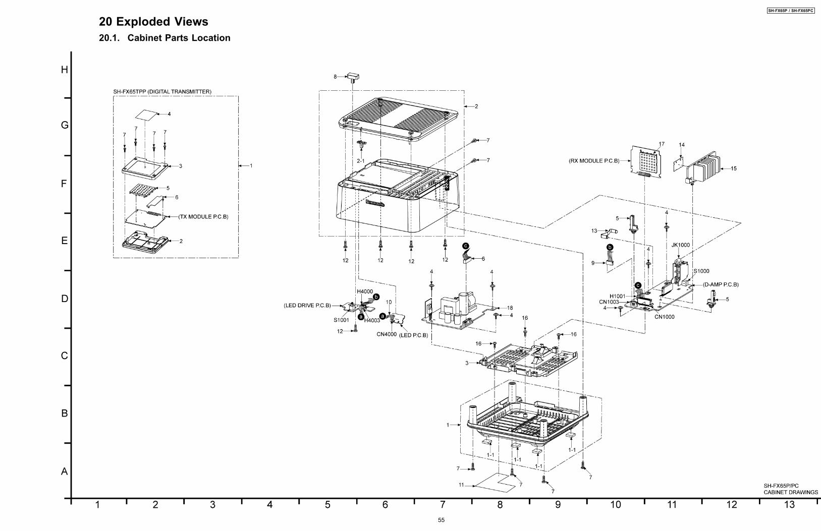
20 Exploded Views20.1. Cabinet Parts Location
SH-FX65P / SH-FX65PC
55
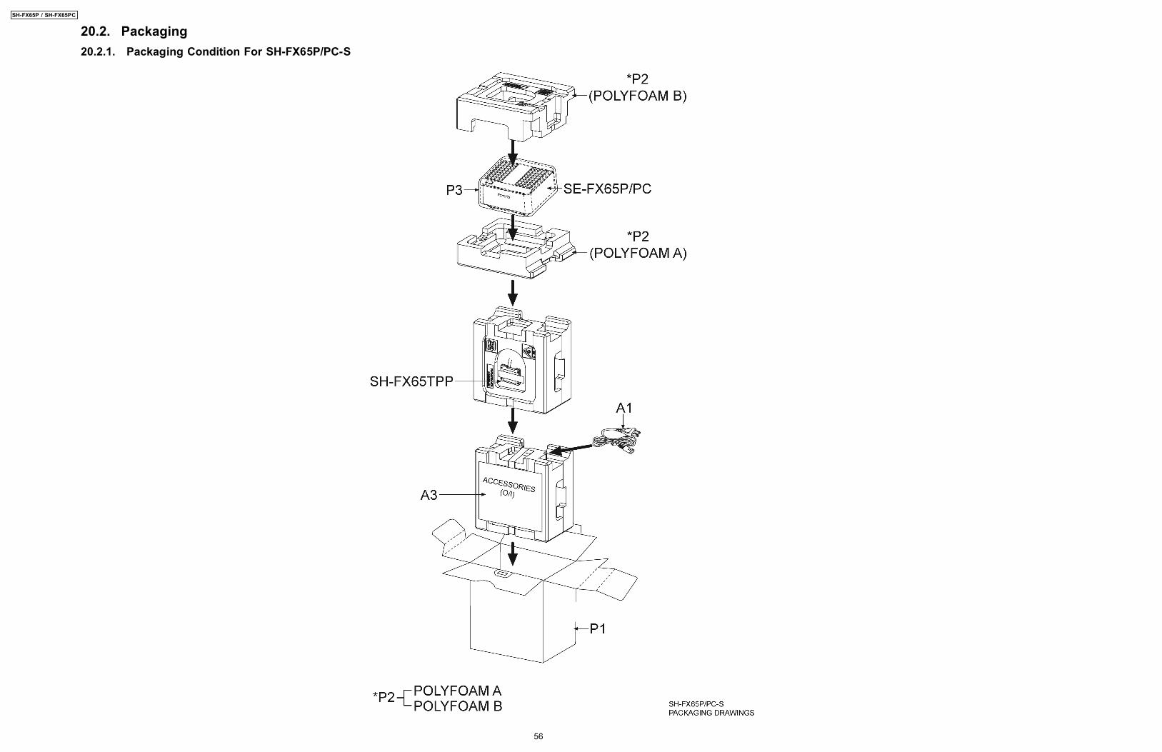
20.2. Packaging20.2.1. Packaging Condition For SH-FX65P/PC-S
SH-FX65P / SH-FX65PC
56
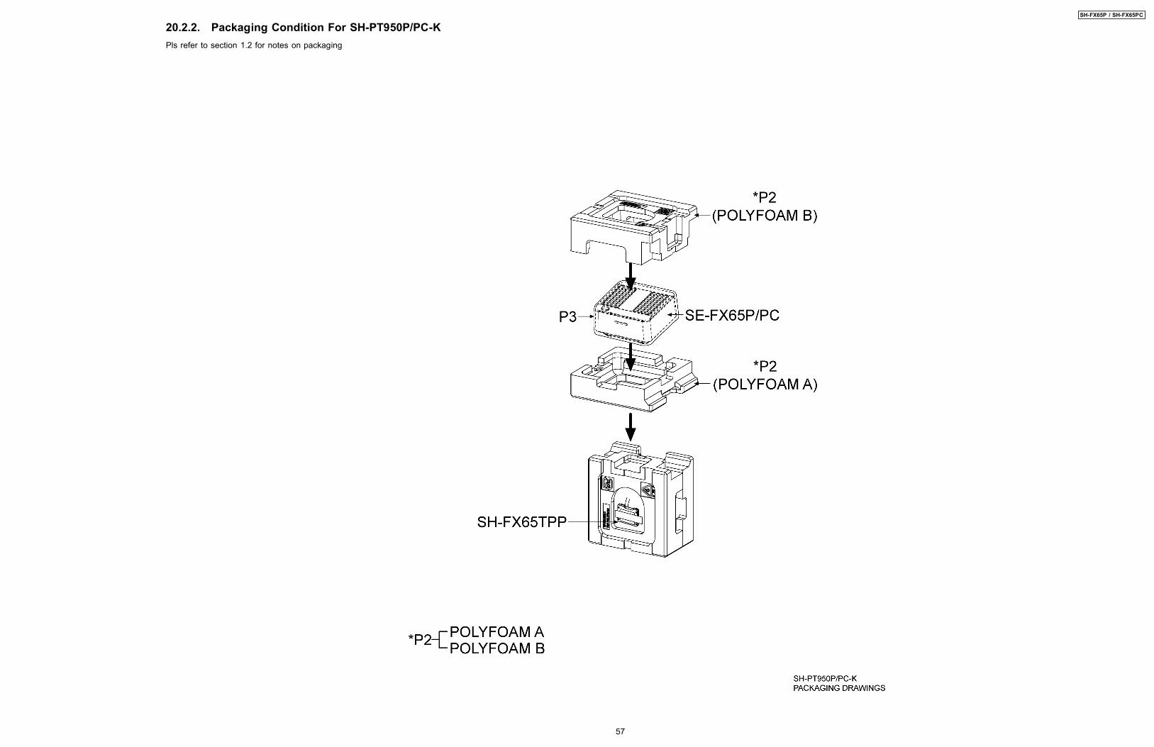
20.2.2. Packaging Condition For SH-PT950P/PC-KPls refer to section 1.2 for notes on packaging
SH-FX65P / SH-FX65PC
57
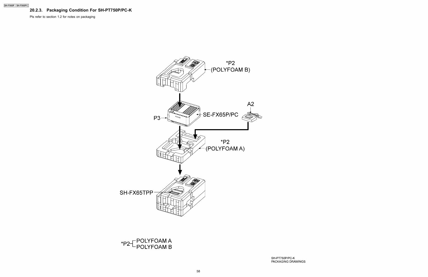
20.2.3. Packaging Condition For SH-PT750P/PC-KPls refer to section 1.2 for notes on packaging
SH-FX65P / SH-FX65PC
58
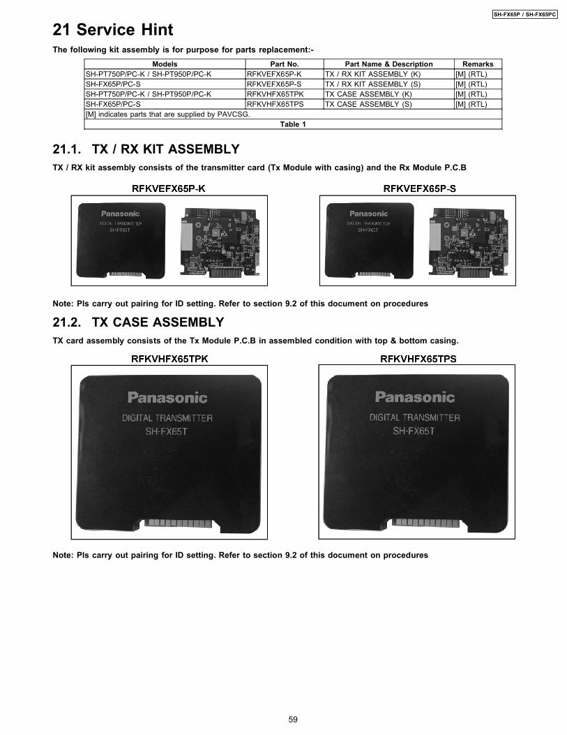
21 Service HintThe following kit assembly is for purpose for parts replacement:-
Models Part No. Part Name & Description RemarksSH-PT750P/PC-K / SH-PT950P/PC-K RFKVEFX65P-K TX / RX KIT ASSEMBLY (K) [M] (RTL)SH-FX65P/PC-S RFKVEFX65P-S TX / RX KIT ASSEMBLY (S) [M] (RTL)SH-PT750P/PC-K / SH-PT950P/PC-K RFKVHFX65TPK TX CASE ASSEMBLY (K) [M] (RTL)SH-FX65P/PC-S RFKVHFX65TPS TX CASE ASSEMBLY (S) [M] (RTL)[M] indicates parts that are supplied by PAVCSG.
Table 1
21.1. TX / RX KIT ASSEMBLYTX / RX kit assembly consists of the transmitter card (Tx Module with casing) and the Rx Module P.C.B
Note: Pls carry out pairing for ID setting. Refer to section 9.2 of this document on procedures
21.2. TX CASE ASSEMBLYTX card assembly consists of the Tx Module P.C.B in assembled condition with top & bottom casing.
Note: Pls carry out pairing for ID setting. Refer to section 9.2 of this document on procedures
59
SH-FX65P / SH-FX65PC
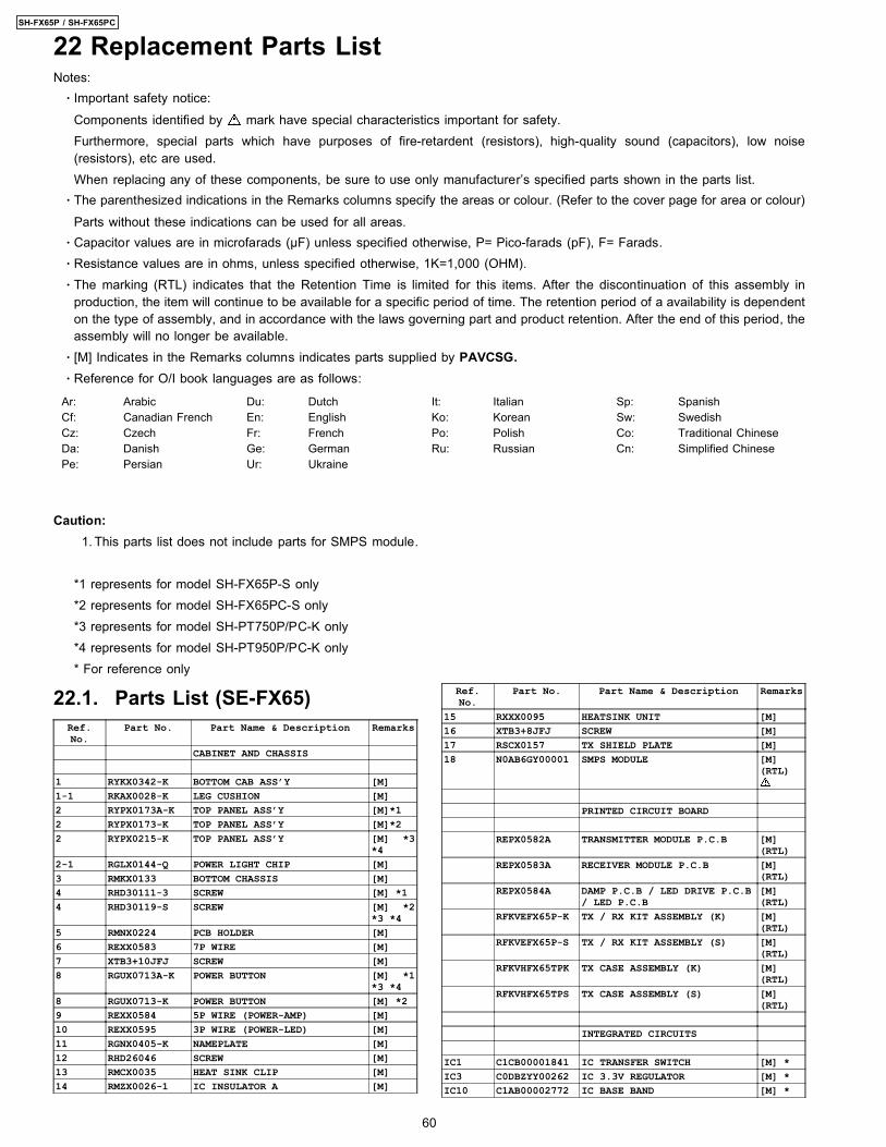
Notes:
22.1. Parts List (SE-FX65)Ref.No.
Part No. Part Name & Description Remarks
CABINET AND CHASSIS
1 RYKX0342-K BOTTOM CAB ASS’Y [M]1-1 RKAX0028-K LEG CUSHION [M]2 RYPX0173A-K TOP PANEL ASS’Y [M]*12 RYPX0173-K TOP PANEL ASS’Y [M]*22 RYPX0215-K TOP PANEL ASS’Y [M] *3
*42-1 RGLX0144-Q POWER LIGHT CHIP [M]3 RMKX0133 BOTTOM CHASSIS [M]4 RHD30111-3 SCREW [M] *14 RHD30119-S SCREW [M] *2
*3 *45 RMNX0224 PCB HOLDER [M]6 REXX0583 7P WIRE [M]7 XTB3+10JFJ SCREW [M]8 RGUX0713A-K POWER BUTTON [M] *1
*3 *48 RGUX0713-K POWER BUTTON [M] *29 REXX0584 5P WIRE (POWER-AMP) [M]10 REXX0595 3P WIRE (POWER-LED) [M]11 RGNX0405-K NAMEPLATE [M]12 RHD26046 SCREW [M]13 RMCX0035 HEAT SINK CLIP [M]14 RMZX0026-1 IC INSULATOR A [M]
Ref.No.
Part No. Part Name & Description Remarks
15 RXXX0095 HEATSINK UNIT [M]16 XTB3+8JFJ SCREW [M]17 RSCX0157 TX SHIELD PLATE [M]18 N0AB6GY00001 SMPS MODULE [M]
(RTL)
PRINTED CIRCUIT BOARD
REPX0582A TRANSMITTER MODULE P.C.B [M](RTL)
REPX0583A RECEIVER MODULE P.C.B [M](RTL)
REPX0584A DAMP P.C.B / LED DRIVE P.C.B/ LED P.C.B
[M](RTL)
RFKVEFX65P-K TX / RX KIT ASSEMBLY (K) [M](RTL)
RFKVEFX65P-S TX / RX KIT ASSEMBLY (S) [M](RTL)
RFKVHFX65TPK TX CASE ASSEMBLY (K) [M](RTL)
RFKVHFX65TPS TX CASE ASSEMBLY (S) [M](RTL)
INTEGRATED CIRCUITS
IC1 C1CB00001841 IC TRANSFER SWITCH [M] *IC3 C0DBZYY00262 IC 3.3V REGULATOR [M] *IC10 C1AB00002772 IC BASE BAND [M] *
22 Replacement Parts List
· Important safety notice:
Components identified by mark have special characteristics important for safety.Furthermore, special parts which have purposes of fire-retardent (resistors), high-quality sound (capacitors), low noise(resistors), etc are used.When replacing any of these components, be sure to use only manufacturer’s specified parts shown in the parts list.
· The parenthesized indications in the Remarks columns specify the areas or colour. (Refer to the cover page for area or colour)
Parts without these indications can be used for all areas. · Capacitor values are in microfarads (µF) unless specified otherwise, P= Pico-farads (pF), F= Farads. · Resistance values are in ohms, unless specified otherwise, 1K=1,000 (OHM). · The marking (RTL) indicates that the Retention Time is limited for this items. After the discontinuation of this assembly in
production, the item will continue to be available for a specific period of time. The retention period of a availability is dependenton the type of assembly, and in accordance with the laws governing part and product retention. After the end of this period, theassembly will no longer be available.
· [M] Indicates in the Remarks columns indicates parts supplied by PAVCSG. · Reference for O/I book languages are as follows:
Ar: Arabic Du: Dutch It: Italian Sp: SpanishCf: Canadian French En: English Ko: Korean Sw: SwedishCz: Czech Fr: French Po: Polish Co: Traditional ChineseDa: Danish Ge: German Ru: Russian Cn: Simplified ChinesePe: Persian Ur: Ukraine
Caution: 1. This parts list does not include parts for SMPS module.
*1 represents for model SH-FX65P-S only*2 represents for model SH-FX65PC-S only*3 represents for model SH-PT750P/PC-K only*4 represents for model SH-PT950P/PC-K only* For reference only
60
SH-FX65P / SH-FX65PC
Ref.No.
Part No. Part Name & Description Remarks
IC13 C1CB00002648 IC RF [M] *IC1000 C2BBED000056 IC MCU [M]IC1102 C0CBCBC00090 IC 3.3V REGULATOR [M]IC1103 C0CBCBC00090 IC 3.3V REGULATOR [M]IC1105 C1BB00001071 IC POWER ON RESET [M]IC1400 C0FBBK000066 IC DAC [M]IC3001 C0ABBB000067 IC OP AMP [M]IC3002 C0ABBB000067 IC OP AMP [M]IC5200 C1BA00000487 IC DIGITAL HIC (CLASS-D AMP) [M]
TRANSISTORS
Q1003 B1ACKD000006 TRANSISTOR [M]Q1004 B1ADCE000012 TRANSISTOR [M]Q1005 B1GBCFJJ0051 TRANSISTOR [M]Q1006 B1GBCFJJ0051 TRANSISTOR [M]Q1007 B1ABCF000176 TRANSISTOR [M]Q1008 B1ABCF000176 TRANSISTOR [M]Q1009 B1GBCFJJ0051 TRANSISTOR [M]Q1010 B1GDCFJJ0047 TRANSISTOR [M]Q1011 B1AAKD000012 TRANSISTOR [M]Q2002 B1AAKD000012 TRANSISTOR [M]Q2010 B1ACCF000094 TRANSISTOR [M]Q2011 B1ACKD000006 TRANSISTOR [M]Q4000 B1GBCFJJ0051 TRANSISTOR [M]Q4001 B1GDCFJJ0047 TRANSISTOR [M]
DIODES
D1000 B0ECKP000002 DIODE [M]D2000 B0BC01600013 DIODE [M]D4000 B0ACCK000005 DIODE [M]D4001 B3AGA0000122 DIODE [M]
SWITCHES
S1000 EVQPC105K SW ID SET [M]S1001 K0F122B00107 SW POWER [M]
CONNECTORS
CN1000 K1MY22A00003 TRAN/CARD CONNECTOR [M]CN1003 K1KA05AA0193 5P CONNECTOR [M]CN4000 K1YZ03000010 3P CABLE HOLDER [M]
COILS & TRANSFORMERS
L15 F1G1HR56A561 INDUCTOR [M] *L16 G1C3N9ZA0068 INDUCTOR [M] *L17 G1C3N9ZA0068 INDUCTOR [M] *L20 G1C4N7ZA0068 INDUCTOR [M] *L21 G1C4N7ZA0068 INDUCTOR [M] *L1000 G0A150L00003 LINE CHOKE COIL [M]L1001 G0B9R5K00003 LINE CHOKE COIL [M]L1002 G0B9R5K00003 LINE CHOKE COIL [M]L1003 J0JKB0000020 EMI BEAD CORE [M]L1004 J0JKB0000020 EMI BEAD CORE [M]L1101 ERJ2GE0R00X CHIP JUMPER [M]
COMPONENT COMBINATION
Z1000 K4CZ01000027 TERMINAL [M]Z1001 K4CZ01000027 TERMINAL [M]Z1002 K4CZ01000027 TERMINAL [M]
Y1 H0J122500037 CRYSTAL [M] *Y2 H0J220500001 CRYSTAL [M] *
HOLDERS
H1001 K1YF07000003 7P WIRE HOLDER [M]H4000 K1YZ05000005 5P CABLE HOLDER [M]H4003 K1YZ03000010 3P CABLE HOLDER [M]
Ref.No.
Part No. Part Name & Description Remarks
JACKS
JK1000 K4BC04B00107 JK SPEAKER [M]
WIRES
W1 ERJ6GEY0R00V CHIP RESISTOR [M] *W3 ERJ6GEY0R00V CHIP RESISTOR [M] *W4 ERJ6GEY0R00V CHIP RESISTOR [M] *W1002 ERJ3GEY0R00V CHIP JUMPER [M]W1003 ERJ3GEY0R00V CHIP JUMPER [M]W1023 ERJ6GEY0R00V CHIP RESISTOR [M]W1024 ERJ3GEY0R00V CHIP JUMPER [M]W1025 ERJ6GEY0R00V CHIP RESISTOR [M]W1031 ERJ3GEY0R00V CHIP JUMPER [M]
PACKING MATERIALS
P1 RPKX0038 GIFT BOX [M] *1P1 RPKX0039 GIFT BOX [M] *2P2 RPNX0459 POLYFOAM [M] *1
*2 *4P2 RPNX0466 POLYFOAM [M] *3P3 RPFX0203 MIRAMAT BAG [M]
ACCESSORIES
A1 K2CB2CB00018 AC CORD [M]*1 *2
A2 RFE0205 I-POD CRADLE [M] *3A3 RQTX0047-Y O/I BOOK [M] *1
*2
RESISTORS
R1 G1C2N7ZA0068 INDUCTOR [M] *R4 ERJ2GEJ823X 82K 1/32W [M] *R5 ERJ2GEJ100X 10 1/32W [M] *R6 G1C2N7ZA0068 INDUCTOR [M] *R7 ERJ2GEJ103X 10K 1/32W [M] *R8 ERJ2GEJ182X 1.8K 1/32W [M] *R9 ERJ2GEJ102X 1K 1/32W [M] *R10 ERJ2GEJ182X 1.8K 1/32W [M] *R11 ERJ2GEJ102X 1K 1/32W [M] *R13 ERJ2GEJ103X 10K 1/32W [M] *R15 G1C47NJA0048 INDUCTOR [M] *R18 ERJ2GEJ103X 10K 1/32W [M] *R19 ERJ2GEJ182X 1.8K 1/32W [M] *R21 ERJ2GE0R00X 0 1/32W [M] *R22 ERJ2GEJ102X 1K 1/32W [M] *R24 ERJ2GEJ682X 6.8K 1/32W [M] *R25 ERJ2GEJ182X 1.8K 1/32W [M] *R26 ERJ2GEJ102X 1K 1/32W [M] *R27 ERJ2GEJ103X 10K 1/32W [M] *R28 ERJ2GEJ222X 2.2K 1/32W [M] *R38 ERJ2GE0R00X 0 1/32W [M] *R39 ERJ2GE0R00X 0 1/32W [M] *R41 ERJ2GEJ103X 10K 1/32W [M] *R43 ERJ2GE0R00X 0 1/32W [M] *R44 ERJ2GE0R00X 0 1/32W [M] *R45 ERJ2GEJ100X 10 1/32W [M] *R46 ERJ2GE0R00X 0 1/32W [M] *R47 ERJ2GE0R00X 0 1/32W [M] *R1000 ERJ3GEYJ473V 47K 1/16W [M]R1001 ERG2SJ122E 1.2K 2W [M]R1001 ERJ2GEJ472X 4.7K 1/32W [M]R1002 ERG2SJ122E 1.2K 2W [M]R1002 ERJ2GEJ472X 4.7K 1/32W [M]R1003 ERJ2GEJ103X 10K 1/32W [M]R1004 ERJ2GEJ103X 10K 1/32W [M]R1005 ERJ2GEJ103X 10K 1/32W [M]R1006 ERJ2GEJ222X 2.2K 1/32W [M]R1007 ERJ2GEJ103X 10K 1/32W [M]
61
SH-FX65P / SH-FX65PC
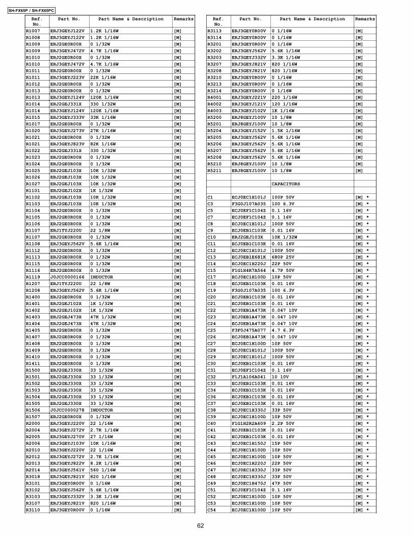
Ref.No.
Part No. Part Name & Description Remarks
R1007 ERJ3GEYJ122V 1.2K 1/16W [M]R1008 ERJ3GEYJ122V 1.2K 1/16W [M]R1009 ERJ2GE0R00X 0 1/32W [M]R1009 ERJ3GEYJ472V 4.7K 1/16W [M]R1010 ERJ2GE0R00X 0 1/32W [M]R1010 ERJ3GEYJ472V 4.7K 1/16W [M]R1011 ERJ2GE0R00X 0 1/32W [M]R1011 ERJ3GEYJ223V 22K 1/16W [M]R1012 ERJ2GE0R00X 0 1/32W [M]R1013 ERJ2GE0R00X 0 1/32W [M]R1013 ERJ3GEYJ124V 120K 1/16W [M]R1014 ERJ2GEJ331X 330 1/32W [M]R1014 ERJ3GEYJ124V 120K 1/16W [M]R1015 ERJ3GEYJ333V 33K 1/16W [M]R1017 ERJ2GE0R00X 0 1/32W [M]R1020 ERJ3GEYJ273V 27K 1/16W [M]R1021 ERJ2GE0R00X 0 1/32W [M]R1021 ERJ3GEYJ823V 82K 1/16W [M]R1022 ERJ2GEJ331X 330 1/32W [M]R1023 ERJ2GE0R00X 0 1/32W [M]R1024 ERJ2GE0R00X 0 1/32W [M]R1025 ERJ2GEJ103X 10K 1/32W [M]R1026 ERJ2GEJ103X 10K 1/32W [M]R1027 ERJ2GEJ103X 10K 1/32W [M]R1101 ERJ2GEJ102X 1K 1/32W [M]R1102 ERJ2GEJ103X 10K 1/32W [M]R1103 ERJ2GEJ103X 10K 1/32W [M]R1104 ERJ2GE0R00X 0 1/32W [M]R1105 ERJ2GE0R00X 0 1/32W [M]R1106 ERJ2GE0R00X 0 1/32W [M]R1107 ERJ1TYJ220U 22 1/8W [M]R1107 ERJ2GE0R00X 0 1/32W [M]R1108 ERJ3GEYJ562V 5.6K 1/16W [M]R1112 ERJ2GE0R00X 0 1/32W [M]R1113 ERJ2GE0R00X 0 1/32W [M]R1115 ERJ2GE0R00X 0 1/32W [M]R1116 ERJ2GE0R00X 0 1/32W [M]R1119 J0JCC0000166 INDUCTOR [M]R1207 ERJ1TYJ220U 22 1/8W [M]R1208 ERJ3GEYJ562V 5.6K 1/16W [M]R1400 ERJ2GE0R00X 0 1/32W [M]R1401 ERJ2GEJ102X 1K 1/32W [M]R1402 ERJ2GEJ102X 1K 1/32W [M]R1403 ERJ2GEJ473X 47K 1/32W [M]R1404 ERJ2GEJ473X 47K 1/32W [M]R1405 ERJ2GE0R00X 0 1/32W [M]R1407 ERJ2GE0R00X 0 1/32W [M]R1408 ERJ2GE0R00X 0 1/32W [M]R1409 ERJ2GE0R00X 0 1/32W [M]R1410 ERJ2GE0R00X 0 1/32W [M]R1411 ERJ2GE0R00X 0 1/32W [M]R1500 ERJ2GEJ330X 33 1/32W [M]R1501 ERJ2GEJ330X 33 1/32W [M]R1502 ERJ2GEJ330X 33 1/32W [M]R1503 ERJ2GEJ330X 33 1/32W [M]R1504 ERJ2GEJ330X 33 1/32W [M]R1505 ERJ2GEJ330X 33 1/32W [M]R1506 J0JCC0000278 INDUCTOR [M]R1507 ERJ2GE0R00X 0 1/32W [M]R2000 ERJ3GEYJ220V 22 1/16W [M]R2004 ERJ3GEYJ272V 2.7K 1/16W [M]R2005 ERJ3GEYJ270V 27 1/16W [M]R2006 ERJ3GEYJ103V 10K 1/16W [M]R2010 ERJ3GEYJ220V 22 1/16W [M]R2012 ERJ3GEYJ272V 2.7K 1/16W [M]R2013 ERJ3GEYJ822V 8.2K 1/16W [M]R2014 ERJ3GEYJ561V 560 1/16W [M]R3018 ERJ3GEYJ821V 820 1/16W [M]R3101 ERJ3GEY0R00V 0 1/16W [M]R3102 ERJ3GEYJ562V 5.6K 1/16W [M]R3103 ERJ3GEYJ332V 3.3K 1/16W [M]R3107 ERJ3GEYJ821V 820 1/16W [M]R3110 ERJ3GEY0R00V 0 1/16W [M]
Ref.No.
Part No. Part Name & Description Remarks
R3113 ERJ3GEY0R00V 0 1/16W [M]R3114 ERJ3GEY0R00V 0 1/16W [M]R3201 ERJ3GEY0R00V 0 1/16W [M]R3202 ERJ3GEYJ562V 5.6K 1/16W [M]R3203 ERJ3GEYJ332V 3.3K 1/16W [M]R3207 ERJ3GEYJ821V 820 1/16W [M]R3208 ERJ3GEYJ821V 820 1/16W [M]R3210 ERJ3GEY0R00V 0 1/16W [M]R3213 ERJ3GEY0R00V 0 1/16W [M]R3214 ERJ3GEY0R00V 0 1/16W [M]R4001 ERJ3GEYJ221V 220 1/16W [M]R4002 ERJ3GEYJ121V 120 1/16W [M]R4003 ERJ3GEYJ102V 1K 1/16W [M]R5200 ERJ8GEYJ100V 10 1/8W [M]R5201 ERJ8GEYJ100V 10 1/8W [M]R5204 ERJ3GEYJ152V 1.5K 1/16W [M]R5205 ERJ3GEYJ562V 5.6K 1/16W [M]R5206 ERJ3GEYJ562V 5.6K 1/16W [M]R5207 ERJ3GEYJ562V 5.6K 1/16W [M]R5208 ERJ3GEYJ562V 5.6K 1/16W [M]R5210 ERJ8GEYJ100V 10 1/8W [M]R5211 ERJ8GEYJ100V 10 1/8W [M]
CAPACITORS
C1 ECJ0EC1H101J 100P 50V [M] *C3 F3G0J107A035 100 6.3V [M] *C5 ECJ0EF1C104Z 0.1 16V [M] *C7 ECJ0EF1C104Z 0.1 16V [M] *C8 ECJ0EC1H101J 100P 50V [M] *C9 ECJ0EB1C103K 0.01 16V [M] *C10 ERJ2GEJ103X 10K 1/32W [M] *C11 ECJ0EB1C103K 0.01 16V [M] *C12 ECJ0EC1H101J 100P 50V [M] *C13 ECJ0EB1E681K 680P 25V [M] *C14 ECJ0EC1H220J 22P 50V [M] *C15 F1G1H4R7A564 4.7P 50V [M] *C17 ECJ0EC1H100D 10P 50V [M] *C18 ECJ0EB1C103K 0.01 16V [M] *C19 F3G0J107A035 100 6.3V [M] *C20 ECJ0EB1C103K 0.01 16V [M] *C21 ECJ0EB1C103K 0.01 16V [M] *C22 ECJ0EB1A473K 0.047 10V [M] *C23 ECJ0EB1A473K 0.047 10V [M] *C24 ECJ0EB1A473K 0.047 10V [M] *C25 F3F0J475A077 4.7 6.3V [M] *C26 ECJ0EB1A473K 0.047 10V [M] *C27 ECJ0EC1H100D 10P 50V [M] *C28 ECJ0EC1H101J 100P 50V [M] *C29 ECJ0EC1H101J 100P 50V [M] *C30 ECJ0EB1C103K 0.01 16V [M] *C31 ECJ0EF1C104Z 0.1 16V [M] *C32 F1J1A106A041 10 10V [M] *C33 ECJ0EB1C103K 0.01 16V [M] *C34 ECJ0EB1C103K 0.01 16V [M] *C36 ECJ0EB1C103K 0.01 16V [M] *C37 ECJ0EB1C103K 0.01 16V [M] *C38 ECJ0EC1H330J 33P 50V [M] *C39 ECJ0EC1H100D 10P 50V [M] *C40 F1G1H2R2A609 2.2P 50V [M] *C41 ECJ0EB1C103K 0.01 16V [M] *C42 ECJ0EB1C103K 0.01 16V [M] *C43 ECJ0EC1H150J 15P 50V [M] *C44 ECJ0EC1H100D 10P 50V [M] *C45 ECJ0EC1H100D 10P 50V [M] *C46 ECJ0EC1H220J 22P 50V [M] *C47 ECJ0EC1H330J 33P 50V [M] *C48 ECJ0EC1H330J 33P 50V [M] *C49 ECJ0EC1H470J 47P 50V [M] *C51 ECJ0EF1C104Z 0.1 16V [M] *C52 ECJ0EC1H100D 10P 50V [M] *C53 ECJ0EC1H100D 10P 50V [M] *C54 ECJ0EC1H100D 10P 50V [M] *
62
SH-FX65P / SH-FX65PC
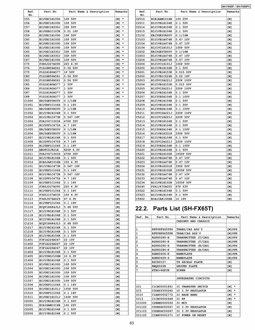
Ref.No.
Part No. Part Name & Description Remarks
C55 ECJ0EC1H100D 10P 50V [M] *C56 ECJ0EC1H100D 10P 50V [M] *C57 ECJ0EC1H330J 33P 50V [M] *C58 ECJ0EB1C103K 0.01 16V [M] *C59 ECJ0EC1H100D 10P 50V [M] *C60 ECJ0EC1H100D 10P 50V [M] *C61 ECJ0EC1H100D 10P 50V [M] *C62 ECJ0EC1H100D 10P 50V [M] *C65 ECJ0EC1H330J 33P 50V [M] *C66 ECJ0EC1H330J 33P 50V [M] *C67 ECJ0EC1H100D 10P 50V [M] *C70 F3H0J227A090 220 6.3V [M] *C74 F1G1HR56A561 0.56 50V [M] *C75 F1G1H1R0A577 1P 50V [M] *C80 F1G1HR56A561 0.56 50V [M] *C83 F1G1HR56A561 0.56 50V [M] *C85 F1G1H1R0A577 1 50V [M] *C86 F1G1H1R0A577 1 50V [M] *C87 F1G1H1R0A577 1 50V [M] *C88 F1G1H1R0A577 1 50V [M] *C1000 ERJ3GEY0R00V 0 1/16W [M]C1001 ECJ0EF1C104Z 0.1 16V [M]C1001 ERJ3GEY0R00V 0 1/16W [M]C1002 ECJ1VB1H104K 0.1 50V [M]C1004 ECJ1VB1C473K 0.047 16V [M]C1004 F2A1V4710036 470P 35V [M]C1005 ECJ2FF1C475Z 4.7 16V [M]C1005 ERJ3GEY0R00V 0 1/16W [M]C1006 ERJ3GEY0R00V 0 1/16W [M]C1007 ECJ1VB1H104K 0.1 50V [M]C1008 ECJ2FF1C475Z 4.7 16V [M]C1009 ECJ0EF1C104Z 0.1 16V [M]C1009 EEUFC0J821B 820P 6.3V [M]C1011 F2A1V4710036 470P 35V [M]C1012 ECJ1VB1H104K 0.1 50V [M]C1014 ECA0JAK101XB 100 6.3V [M]C1101 ECJ1VB1C473K 0.047 16V [M]C1102 ECJ0EF1C104Z 0.1 16V [M]C1103 ECJ1VB1C473K 0.047 16V [M]C1108 ECJ2FF1C475Z 4.7 16V [M]C1109 ECJ0EF1C104Z 0.1 16V [M]C1110 F3H0J227A090 220 6.3V [M]C1111 ECJ0EF1C104Z 0.1 16V [M]C1112 F3G0J107A035 100 6.3V [M]C1113 F3G0J476A029 47 6.3V [M]C1114 ECJ0EF1C104Z 0.1 16V [M]C1116 ECQV1H684JL3 0.68 50V [M]C1117 ECJ1VB1H104K 0.1 50V [M]C1118 ECJ1VB1H104K 0.1 50V [M]C1119 ECJ1VB1H104K 0.1 50V [M]C1216 ECQV1H684JL3 0.68 50V [M]C1217 ECJ1VB1H104K 0.1 50V [M]C1218 ECJ1VB1H104K 0.1 50V [M]C1219 ECJ1VB1H104K 0.1 50V [M]C1401 F3F1A226A047 22 10V [M]C1402 F3F1A226A047 22 10V [M]C1403 F3F1A226A047 22 10V [M]C1404 ECJ1VB1H104K 0.1 50V [M]C1405 ECJ3YB0J106M 10 6.3V [M]C1406 ECJ1VB1H104K 0.1 50V [M]C1503 ECJ0EC1H100D 10P 50V [M]C1504 ECJ0EC1H100D 10P 50V [M]C1505 ECJ0EC1H100D 10P 50V [M]C1506 ECJ0EC1H100D 10P 50V [M]C1507 ECJ0EC1H100D 10P 50V [M]C1508 ECJ0EF1C104Z 0.1 16V [M]C1509 ECJ0EC1H101J 100P 50V [M]C1510 ECJ0EF1C104Z 0.1 16V [M]C1511 ECJ0EC1H101J 100P 50V [M]C2000 ECJ1VB1H104K 0.1 50V [M]C2001 ECA1EAM101XB 100 25V [M]C2005 ECJ1VB1H104K 0.1 50V [M]C2006 ECJ1VB1H104K 0.1 50V [M]
Ref.No.
Part No. Part Name & Description Remarks
C2010 ECA1EAM101XB 100 25V [M]C2011 ECJ1VB1H104K 0.1 50V [M]C2014 ECJ1VB1H104K 0.1 50V [M]C2015 ECJ1VB1H104K 0.1 50V [M]C3102 ERJ3GEY0R00V 0 1/16W [M]C3103 ECJ1VB1A474K 0.47 10V [M]C3104 ECJ1VB1A474K 0.47 10V [M]C3106 ECJ1VC1H101J 100P 50V [M]C3202 ERJ3GEY0R00V 0 1/16W [M]C3203 ECJ1VB1A474K 0.47 10V [M]C3204 ECJ1VB1A474K 0.47 10V [M]C3206 ECJ1VC1H101J 100P 50V [M]C5200 ECJ1VB1H104K 0.1 50V [M]C5201 ECJ1VB1H153K 0.015 50V [M]C5202 ECJ1VB1C224K 0.22 16V [M]C5203 ECJ2VC2A221J 220P 100V [M]C5204 ECJ1VB1H153K 0.015 50V [M]C5205 ECJ2VC2A221J 220P 100V [M]C5206 ECJ1VB1H104K 0.1 50V [M]C5207 ECJ3YB2A104K 0.1 100V [M]C5208 ECJ1VB1H104K 0.1 50V [M]C5209 ECJ1VB1H104K 0.1 50V [M]C5210 ECJ3YB2A104K 0.1 100V [M]C5211 ECJ2VC2A221J 220P 100V [M]C5212 ECJ1VC1H221J 220P 50V [M]C5213 ECJ1VB1H104K 0.1 50V [M]C5214 ECJ1VB1H104K 0.1 50V [M]C5215 ECJ3YB2A104K 0.1 100V [M]C5216 ECJ1VB1H331K 330P 50V [M]C5217 ECJ1VB1H104K 0.1 50V [M]C5218 ECJ2VC2A221J 220P 100V [M]C5219 ECJ3YB2A104K 0.1 100V [M]C5220 ECJ1VB1H104K 0.1 50V [M]C5221 ECJ1VB1H102K 1000P 50V [M]C5222 ECJ1VB1A474K 0.47 10V [M]C5223 ECJ1VB1A474K 0.47 10V [M]C5224 ECJ1VB1H331K 330P 50V [M]C5231 ECJ1VB1H102K 1000P 50V [M]C5232 ECJ1VB1A474K 0.47 10V [M]C5233 ECJ1VB1A474K 0.47 10V [M]C5234 ECJ1VB1H102K 1000P 50V [M]C5240 F2A1J470A050 47P 63V [M]C5522 ECJ1VB1H104K 0.1 50V [M]C5523 ECJ1VB1H104K 0.1 50V [M]C5602 ECA1CAK100XB 10 16V [M]
22.2. Parts List (SH-FX65T)Ref. No. Part No. Part Name & Description Remarks
CABINET AND CHASSIS
1 RFKVHFX65TPS TRANS/CAS ASS’Y [M]PPS1 RFKVHFX65TPK TRAN/CAS ASS’Y [M]PPK2 RGPX0285-H TRANSMITTER (T/CAS) [M]PPS2 RGPX0285-K TRANSMITTER (T/CAS) [M]PPK3 RGPX0286-H TRANSMITTER (B/CAS) [M]PPS3 RGPX0286-K TRANSMITTER (B/CAS) [M]PPK4 RGNX0406-K NAMEPLATE [M]PPK4 RGNX0469-S NAMEPLATE [M]PPS5 RSCX0157 TX SHIELD PLATE [M]6 RMQX0268 GROUND PLATE [M]7 XTB2+6GFJK SCREW [M]
INTEGRATED CIRCUITS
IC1 C1CB00001841 IC TRANSFER SWITCH [M] *IC3 C0DBZYY00262 IC 3.3V REGULATOR [M] *IC10 C1AB00002772 IC BASE BAND [M] *IC13 C1CB00002648 IC RF [M] *IC1000 C2BBED000056 IC MCU [M]IC1102 C0DBZGC00067 IC 3.3V REGULATOR [M]IC1103 C0DBZGC00067 IC 3.3V REGULATOR [M]IC1105 C1BB00001071 IC POWER ON RESET [M]
63
SH-FX65P / SH-FX65PC
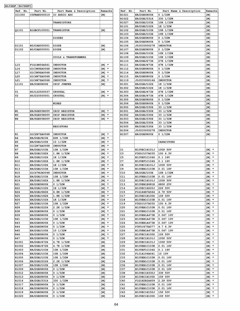
Ref. No. Part No. Part Name & Description RemarksIC1300 C0FBAK000019 IC AUDIO ADC [M]
TRANSISTORS
Q1101 B1GBCFJJ0051 TRANSISTOR [M]
DIODES
D1101 B0JCAE000001 DIODE [M]D1102 B0JCAE000001 DIODE [M]
COILS & TRANSFORMERS
L15 F1G1HR56A561 INDUCTOR [M] *L16 G1C3N9ZA0068 INDUCTOR [M] *L17 G1C3N9ZA0068 INDUCTOR [M] *L20 G1C4N7ZA0068 INDUCTOR [M] *L21 G1C4N7ZA0068 INDUCTOR [M] *L1101 ERJ2GE0R00X CHIP JUMPER [M]
Y1 H0J122500037 CRYSTAL [M] *Y2 H0J220500001 CRYSTAL [M] *
WIRES
W1 ERJ6GEY0R00V CHIP RESISTOR [M] *W3 ERJ6GEY0R00V CHIP RESISTOR [M] *W4 ERJ6GEY0R00V CHIP RESISTOR [M] *
RESISTORS
R1 G1C2N7ZA0068 INDUCTOR [M] *R4 ERJ2GEJ823X 82K 1/32W [M] *R5 ERJ2GEJ100X 10 1/32W [M] *R6 G1C2N7ZA0068 INDUCTOR [M] *R7 ERJ2GEJ103X 10K 1/32W [M] *R8 ERJ2GEJ182X 1.8K 1/32W [M] *R9 ERJ2GEJ102X 1K 1/32W [M] *R10 ERJ2GEJ182X 1.8K 1/32W [M] *R11 ERJ2GEJ102X 1K 1/32W [M] *R13 ERJ2GEJ103X 10K 1/32W [M] *R15 G1C47NJA0048 INDUCTOR [M] *R18 ERJ2GEJ103X 10K 1/32W [M] *R19 ERJ2GEJ182X 1.8K 1/32W [M] *R21 ERJ2GE0R00X 0 1/32W [M] *R22 ERJ2GEJ102X 1K 1/32W [M] *R24 ERJ2GEJ682X 6.8K 1/32W [M] *R25 ERJ2GEJ182X 1.8K 1/32W [M] *R26 ERJ2GEJ102X 1K 1/32W [M] *R27 ERJ2GEJ103X 10K 1/32W [M] *R28 ERJ2GEJ222X 2.2K 1/32W [M] *R38 ERJ2GE0R00X 0 1/32W [M] *R39 ERJ2GE0R00X 0 1/32W [M] *R41 ERJ2GEJ103X 10K 1/32W [M] *R43 ERJ2GE0R00X 0 1/32W [M] *R44 ERJ2GE0R00X 0 1/32W [M] *R45 ERJ2GEJ100X 10 1/32W [M] *R46 ERJ2GE0R00X 0 1/32W [M] *R47 ERJ2GE0R00X 0 1/32W [M] *R1001 ERJ2GEJ472X 4.7K 1/32W [M]R1002 ERJ2GEJ472X 4.7K 1/32W [M]R1003 ERJ2GEJ103X 10K 1/32W [M]R1004 ERJ2GEJ103X 10K 1/32W [M]R1005 ERJ2GEJ103X 10K 1/32W [M]R1006 ERJ2GEJ222X 2.2K 1/32W [M]R1007 ERJ2GEJ103X 10K 1/32W [M]R1009 ERJ2GE0R00X 0 1/32W [M]R1012 ERJ2GE0R00X 0 1/32W [M]R1013 ERJ2GE0R00X 0 1/32W [M]R1014 ERJ2GEJ331X 330 1/32W [M]R1017 ERJ2GE0R00X 0 1/32W [M]R1018 ERJ2GE0R00X 0 1/32W [M]R1019 ERJ2GE0R00X 0 1/32W [M]R1020 ERJ2GE0R00X 0 1/32W [M]
Ref. No. Part No. Part Name & Description RemarksR1021 ERJ2GE0R00X 0 1/32W [M]R1022 ERJ2GEJ331X 330 1/32W [M]R1027 ERJ2GEJ103X 10K 1/32W [M]R1101 ERJ2GEJ102X 1K 1/32W [M]R1102 ERJ2GEJ103X 10K 1/32W [M]R1103 ERJ2GEJ103X 10K 1/32W [M]R1104 ERJ2GE0R00X 0 1/32W [M]R1105 ERJ2GE0R00X 0 1/32W [M]R1106 J0JCC0000278 INDUCTOR [M]R1107 ERJ2GE0R00X 0 1/32W [M]R1108 ERJ2GEJ103X 10K 1/32W [M]R1109 ERJ2GEJ103X 10K 1/32W [M]R1110 ERJ2GEJ273X 27K 1/32W [M]R1111 ERJ2GEJ473X 47K 1/32W [M]R1112 ERJ2GE0R00X 0 1/32W [M]R1114 ERJ2GE0R00X 0 1/32W [M]R1115 ERJ2GE0R00X 0 1/32W [M]R1119 J0JCC0000166 INDUCTOR [M]R1301 ERJ2GEJ102X 1K 1/32W [M]R1302 ERJ2GEJ102X 1K 1/32W [M]R1303 ERJ2GEJ473X 47K 1/32W [M]R1304 ERJ2GEJ473X 47K 1/32W [M]R1305 ERJ2GE0R00X 0 1/32W [M]R1306 ERJ2GE0R00X 0 1/32W [M]R1500 ERJ2GEJ330X 33 1/32W [M]R1501 ERJ2GEJ330X 33 1/32W [M]R1502 ERJ2GEJ330X 33 1/32W [M]R1503 ERJ2GEJ330X 33 1/32W [M]R1504 ERJ2GEJ330X 33 1/32W [M]R1505 ERJ2GEJ330X 33 1/32W [M]R1506 J0JCC0000278 INDUCTOR [M]R1507 ERJ2GE0R00X 0 1/32W [M]
CAPACITORS
C1 ECJ0EC1H101J 100P 50V [M] *C3 F3G0J107A035 100 6.3V [M] *C5 ECJ0EF1C104Z 0.1 16V [M] *C7 ECJ0EF1C104Z 0.1 16V [M] *C8 ECJ0EC1H101J 100P 50V [M] *C9 ECJ0EB1C103K 0.01 16V [M] *C10 ERJ2GEJ103X 10K 1/32W [M] *C11 ECJ0EB1C103K 0.01 16V [M] *C12 ECJ0EC1H101J 100P 50V [M] *C13 ECJ0EB1E681K 680P 25V [M] *C14 ECJ0EC1H220J 22P 50V [M] *C15 F1G1H4R7A564 4.7P 50V [M] *C17 ECJ0EC1H100D 10P 50V [M] *C18 ECJ0EB1C103K 0.01 16V [M] *C19 F3G0J107A035 100 6.3V [M] *C20 ECJ0EB1C103K 0.01 16V [M] *C21 ECJ0EB1C103K 0.01 16V [M] *C22 ECJ0EB1A473K 0.047 10V [M] *C23 ECJ0EB1A473K 0.047 10V [M] *C24 ECJ0EB1A473K 0.047 10V [M] *C25 F3F0J475A077 4.7 6.3V [M] *C26 ECJ0EB1A473K 0.047 10V [M] *C27 ECJ0EC1H100D 10P 50V [M] *C28 ECJ0EC1H101J 100P 50V [M] *C29 ECJ0EC1H101J 100P 50V [M] *C30 ECJ0EB1C103K 0.01 16V [M] *C31 ECJ0EF1C104Z 0.1 16V [M] *C32 F1J1A106A041 10 10V [M] *C33 ECJ0EB1C103K 0.01 16V [M] *C34 ECJ0EB1C103K 0.01 16V [M] *C36 ECJ0EB1C103K 0.01 16V [M] *C37 ECJ0EB1C103K 0.01 16V [M] *C38 ECJ0EC1H330J 33P 50V [M] *C39 ECJ0EC1H100D 10P 50V [M] *C40 F1G1H2R2A609 2.2P 50V [M] *C41 ECJ0EB1C103K 0.01 16V [M] *C42 ECJ0EB1C103K 0.01 16V [M] *C43 ECJ0EC1H150J 15P 50V [M] *C44 ECJ0EC1H100D 10P 50V [M] *
64
SH-FX65P / SH-FX65PC
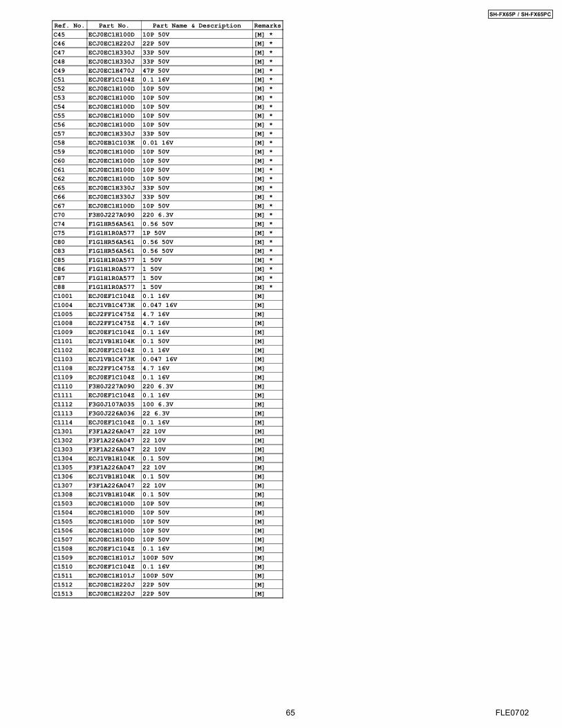
Ref. No. Part No. Part Name & Description RemarksC45 ECJ0EC1H100D 10P 50V [M] *C46 ECJ0EC1H220J 22P 50V [M] *C47 ECJ0EC1H330J 33P 50V [M] *C48 ECJ0EC1H330J 33P 50V [M] *C49 ECJ0EC1H470J 47P 50V [M] *C51 ECJ0EF1C104Z 0.1 16V [M] *C52 ECJ0EC1H100D 10P 50V [M] *C53 ECJ0EC1H100D 10P 50V [M] *C54 ECJ0EC1H100D 10P 50V [M] *C55 ECJ0EC1H100D 10P 50V [M] *C56 ECJ0EC1H100D 10P 50V [M] *C57 ECJ0EC1H330J 33P 50V [M] *C58 ECJ0EB1C103K 0.01 16V [M] *C59 ECJ0EC1H100D 10P 50V [M] *C60 ECJ0EC1H100D 10P 50V [M] *C61 ECJ0EC1H100D 10P 50V [M] *C62 ECJ0EC1H100D 10P 50V [M] *C65 ECJ0EC1H330J 33P 50V [M] *C66 ECJ0EC1H330J 33P 50V [M] *C67 ECJ0EC1H100D 10P 50V [M] *C70 F3H0J227A090 220 6.3V [M] *C74 F1G1HR56A561 0.56 50V [M] *C75 F1G1H1R0A577 1P 50V [M] *C80 F1G1HR56A561 0.56 50V [M] *C83 F1G1HR56A561 0.56 50V [M] *C85 F1G1H1R0A577 1 50V [M] *C86 F1G1H1R0A577 1 50V [M] *C87 F1G1H1R0A577 1 50V [M] *C88 F1G1H1R0A577 1 50V [M] *C1001 ECJ0EF1C104Z 0.1 16V [M]C1004 ECJ1VB1C473K 0.047 16V [M]C1005 ECJ2FF1C475Z 4.7 16V [M]C1008 ECJ2FF1C475Z 4.7 16V [M]C1009 ECJ0EF1C104Z 0.1 16V [M]C1101 ECJ1VB1H104K 0.1 50V [M]C1102 ECJ0EF1C104Z 0.1 16V [M]C1103 ECJ1VB1C473K 0.047 16V [M]C1108 ECJ2FF1C475Z 4.7 16V [M]C1109 ECJ0EF1C104Z 0.1 16V [M]C1110 F3H0J227A090 220 6.3V [M]C1111 ECJ0EF1C104Z 0.1 16V [M]C1112 F3G0J107A035 100 6.3V [M]C1113 F3G0J226A036 22 6.3V [M]C1114 ECJ0EF1C104Z 0.1 16V [M]C1301 F3F1A226A047 22 10V [M]C1302 F3F1A226A047 22 10V [M]C1303 F3F1A226A047 22 10V [M]C1304 ECJ1VB1H104K 0.1 50V [M]C1305 F3F1A226A047 22 10V [M]C1306 ECJ1VB1H104K 0.1 50V [M]C1307 F3F1A226A047 22 10V [M]C1308 ECJ1VB1H104K 0.1 50V [M]C1503 ECJ0EC1H100D 10P 50V [M]C1504 ECJ0EC1H100D 10P 50V [M]C1505 ECJ0EC1H100D 10P 50V [M]C1506 ECJ0EC1H100D 10P 50V [M]C1507 ECJ0EC1H100D 10P 50V [M]C1508 ECJ0EF1C104Z 0.1 16V [M]C1509 ECJ0EC1H101J 100P 50V [M]C1510 ECJ0EF1C104Z 0.1 16V [M]C1511 ECJ0EC1H101J 100P 50V [M]C1512 ECJ0EC1H220J 22P 50V [M]C1513 ECJ0EC1H220J 22P 50V [M]
65
SH-FX65P / SH-FX65PC
FLE0702