What to do with THz? - Wireless Communications · PDF fileWhat to do with THz? Ali M. Niknejad...
23
WCA Futures SIG What to do with THz? Ali M. Niknejad Berkeley Wireless Research Center University of California Berkeley
Transcript of What to do with THz? - Wireless Communications · PDF fileWhat to do with THz? Ali M. Niknejad...
WCA Futures SIG
What to do with THz?
Ali M. Niknejad
Berkeley Wireless Research Center
University of California Berkeley
Outline
• THz Overview
• Potential THz Applications
• THz Transceivers in Silicon?
• Application 1: THz Radar Transceiver
• Application 2: THz Short Range Communication
Slide 1
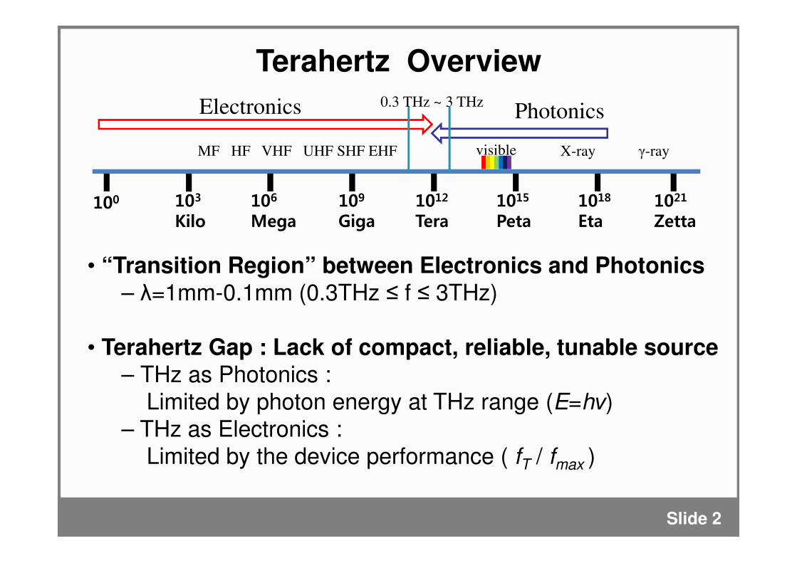
• “Transition Region” between Electronics and Photonics– λ=1mm-0.1mm (0.3THz ≤ f ≤ 3THz)
• Terahertz Gap : Lack of compact, reliable, tunable source – THz as Photonics :
Limited by photon energy at THz range (E=hν)– THz as Electronics :
Limited by the device performance ( fT / fmax )
Terahertz Overview
MF HF VHF UHF SHF EHF X-rayvisible
100 103
Kilo106
Mega109
Giga1012
Tera1015
Peta1018
Eta1021
Zetta
Electronics Photonics0.3 THz ~ 3 THz
γ-ray
Slide 2
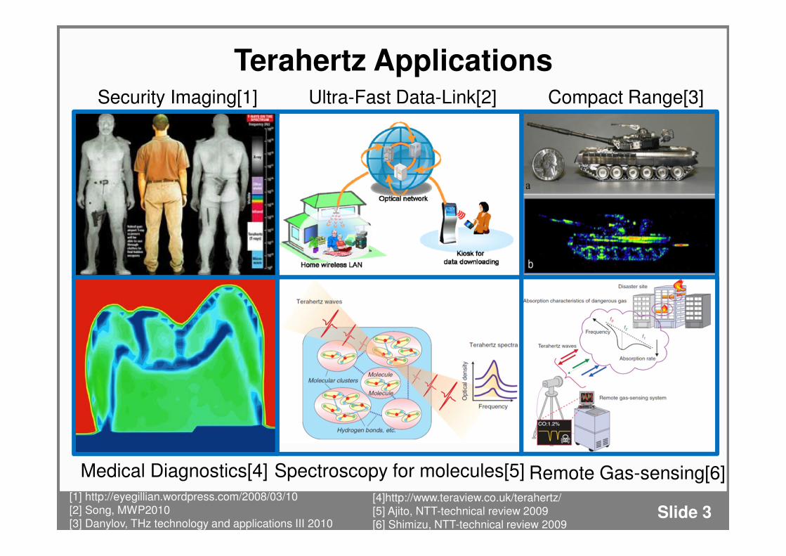
Terahertz Applications
Slide 3[1] http://eyegillian.wordpress.com/2008/03/10[2] Song, MWP2010[3] Danylov, THz technology and applications III 2010
[4]http://www.teraview.co.uk/terahertz/[5] Ajito, NTT-technical review 2009[6] Shimizu, NTT-technical review 2009
Security Imaging[1] Ultra-Fast Data-Link[2] Compact Range[3]
Medical Diagnostics[4] Spectroscopy for molecules[5] Remote Gas-sensing[6]
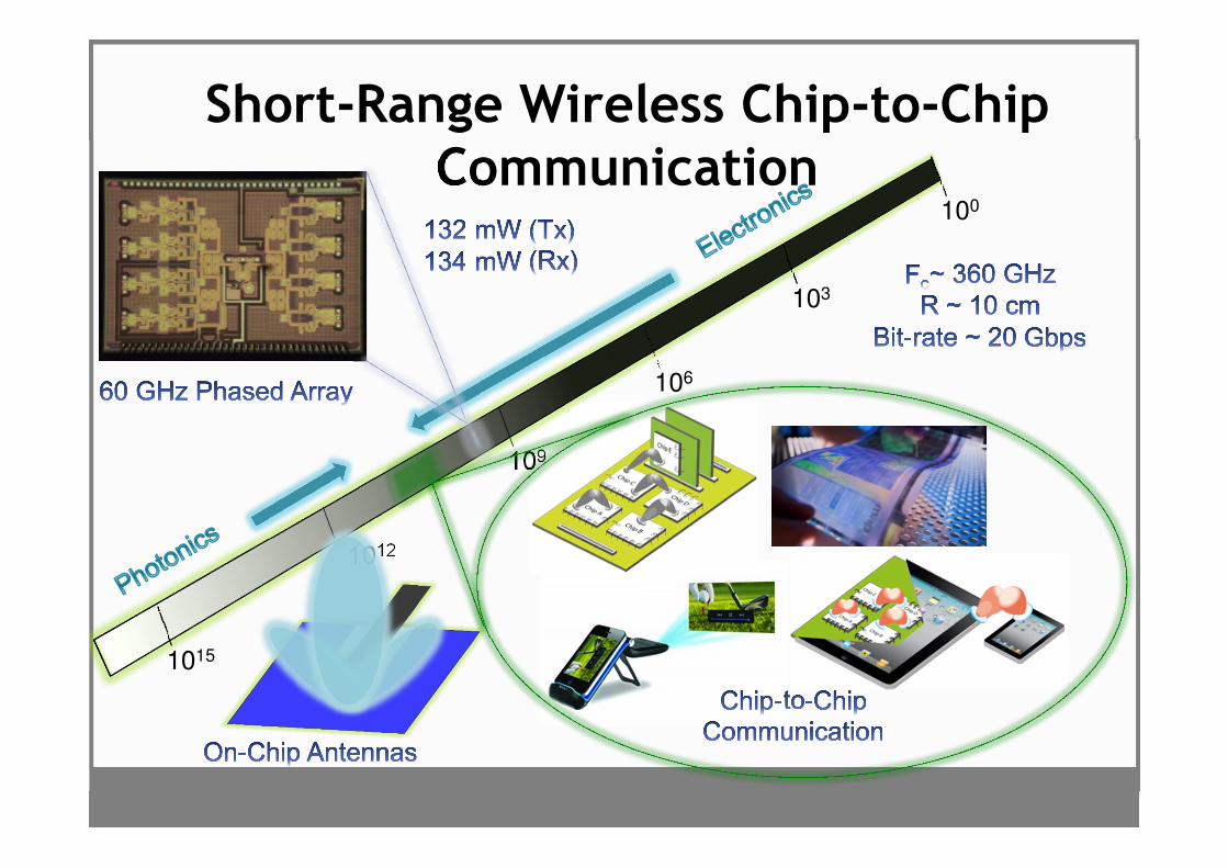
Short-Range Wireless Chip-to-Chip Communication
100
103
106
109
1012
1015
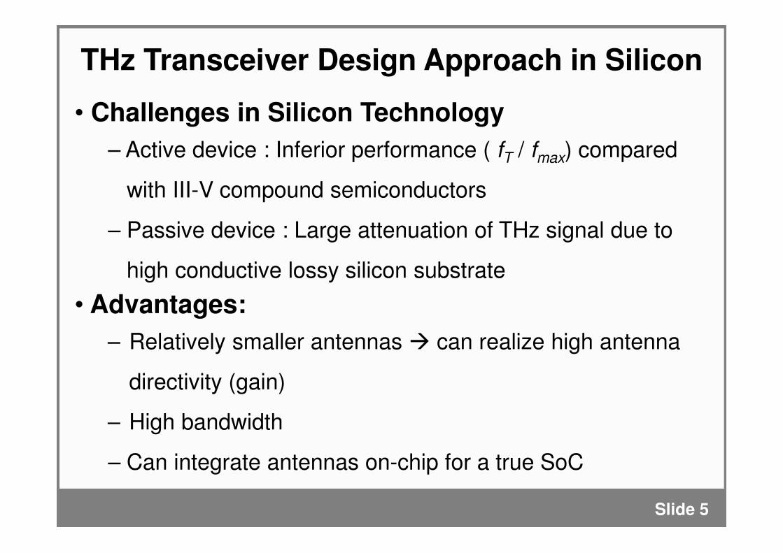
• Challenges in Silicon Technology
– Active device : Inferior performance ( fT / fmax) compared
with III-V compound semiconductors
– Passive device : Large attenuation of THz signal due to
high conductive lossy silicon substrate
• Advantages:
– Relatively smaller antennas � can realize high antenna
directivity (gain)
– High bandwidth
– Can integrate antennas on-chip for a true SoC
THz Transceiver Design Approach in Silicon
Slide 5
WCA Futures SIG
A “THz” Proof of Concept Radar
Jungdong Park, Shinwon Park, Ali M. Niknejad
Slide 6
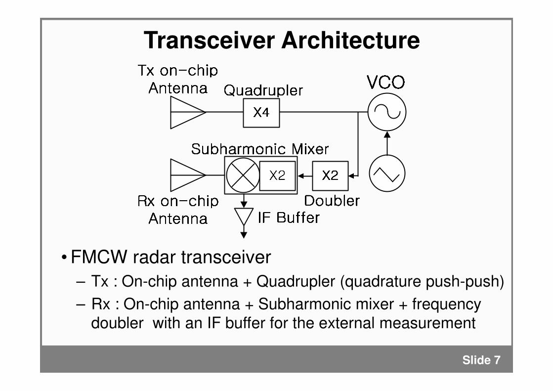
Transceiver Architecture
• FMCW radar transceiver
– Tx : On-chip antenna + Quadrupler (quadrature push-push)
– Rx : On-chip antenna + Subharmonic mixer + frequency doubler with an IF buffer for the external measurement
Slide 7
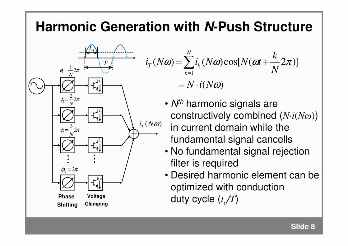
Harmonic Generation with N-Push Structure
Slide 8
)(
)]2(cos[)()(1
ω
πωωω
NiN
N
ktNNiNi
N
k
kT
⋅=
+=∑=
πφ 22
2N
=
πφ 21
1N
=
πφ 23
2N
=
πφ 2=N
••
•
••
•
Shifting
Phase
Clamping
Voltage
1i
2i
3i
Ni
T
0t
)( ωNiT
• Nth harmonic signals are constructively combined (N·i(Nω)) in current domain while the fundamental signal cancells
• No fundamental signal rejection filter is required
• Desired harmonic element can be optimized with conduction duty cycle (to/T)
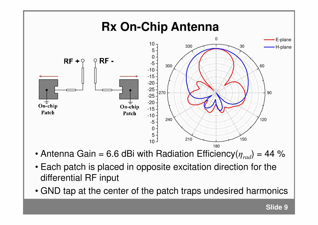
Rx On-Chip Antenna
-25
-20
-15
-10
-5
0
5
100
30
60
90
120
150
180
210
240
270
300
330
-25
-20
-15
-10
-5
0
5
10
E-plane
H-plane
• Antenna Gain = 6.6 dBi with Radiation Efficiency(ηrad) = 44 %
• Each patch is placed in opposite excitation direction for the differential RF input
• GND tap at the center of the patch traps undesired harmonics
Slide 9
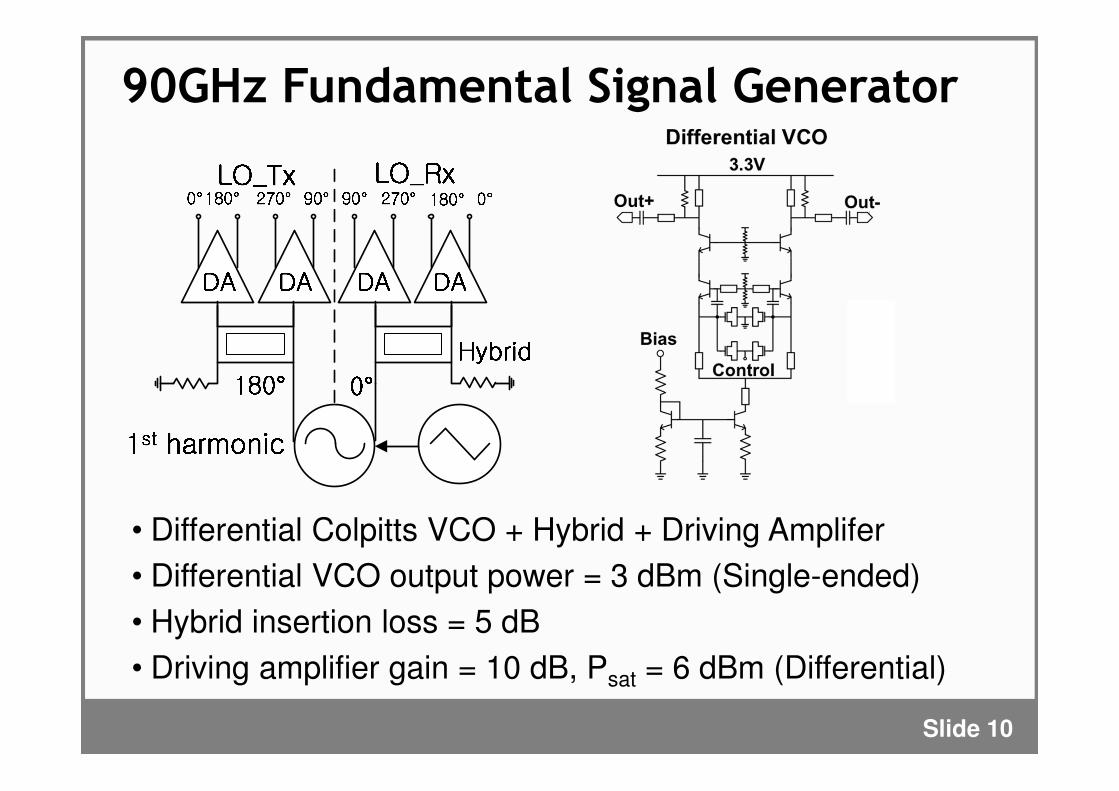
90GHz Fundamental Signal Generator
• Differential Colpitts VCO + Hybrid + Driving Amplifer
• Differential VCO output power = 3 dBm (Single-ended)
• Hybrid insertion loss = 5 dB
• Driving amplifier gain = 10 dB, Psat = 6 dBm (Differential)
Slide 10
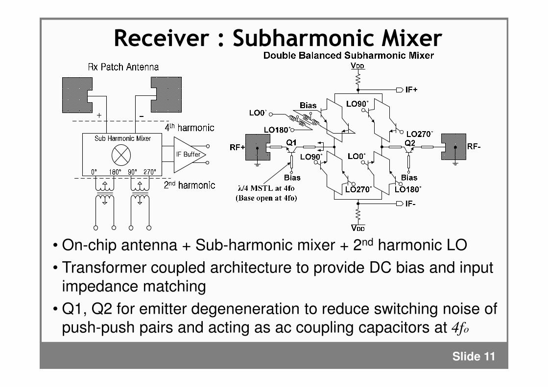
Receiver : Subharmonic Mixer
• On-chip antenna + Sub-harmonic mixer + 2nd harmonic LO
• Transformer coupled architecture to provide DC bias and input impedance matching
• Q1, Q2 for emitter degeneneration to reduce switching noise of push-push pairs and acting as ac coupling capacitors at 4fo
Slide 11
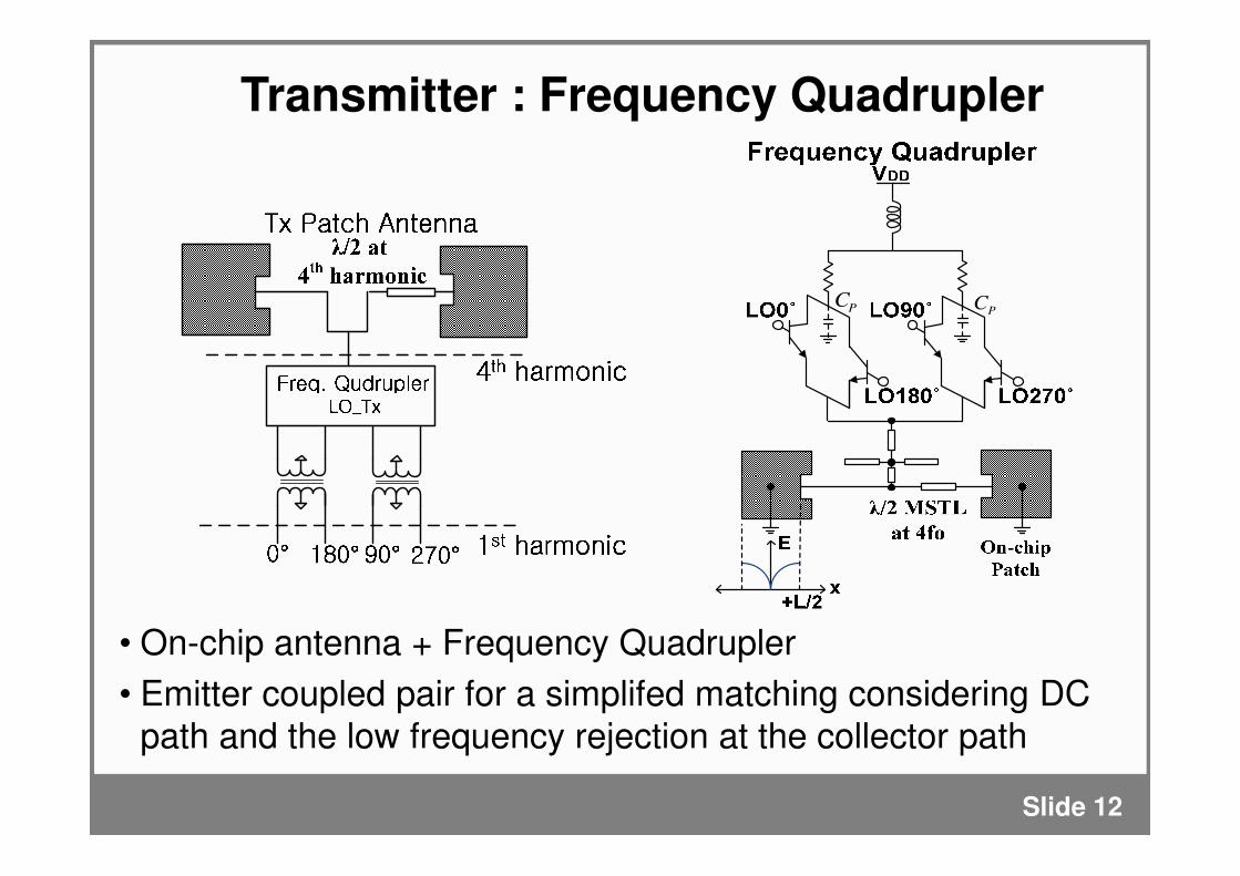
Transmitter : Frequency Quadrupler
• On-chip antenna + Frequency Quadrupler
• Emitter coupled pair for a simplifed matching considering DC path and the low frequency rejection at the collector path
PCPC
Slide 12
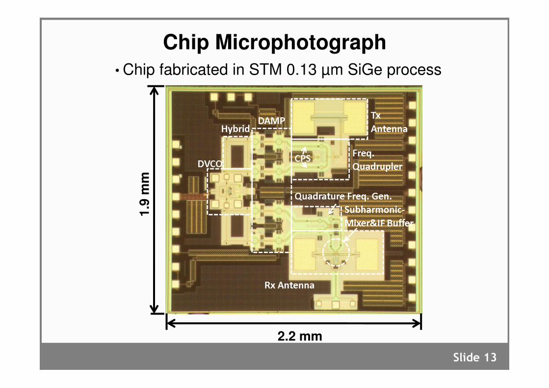
Chip Microphotograph
Slide 13
2.2 mm
1.9
mm
• Chip fabricated in STM 0.13 µm SiGe process
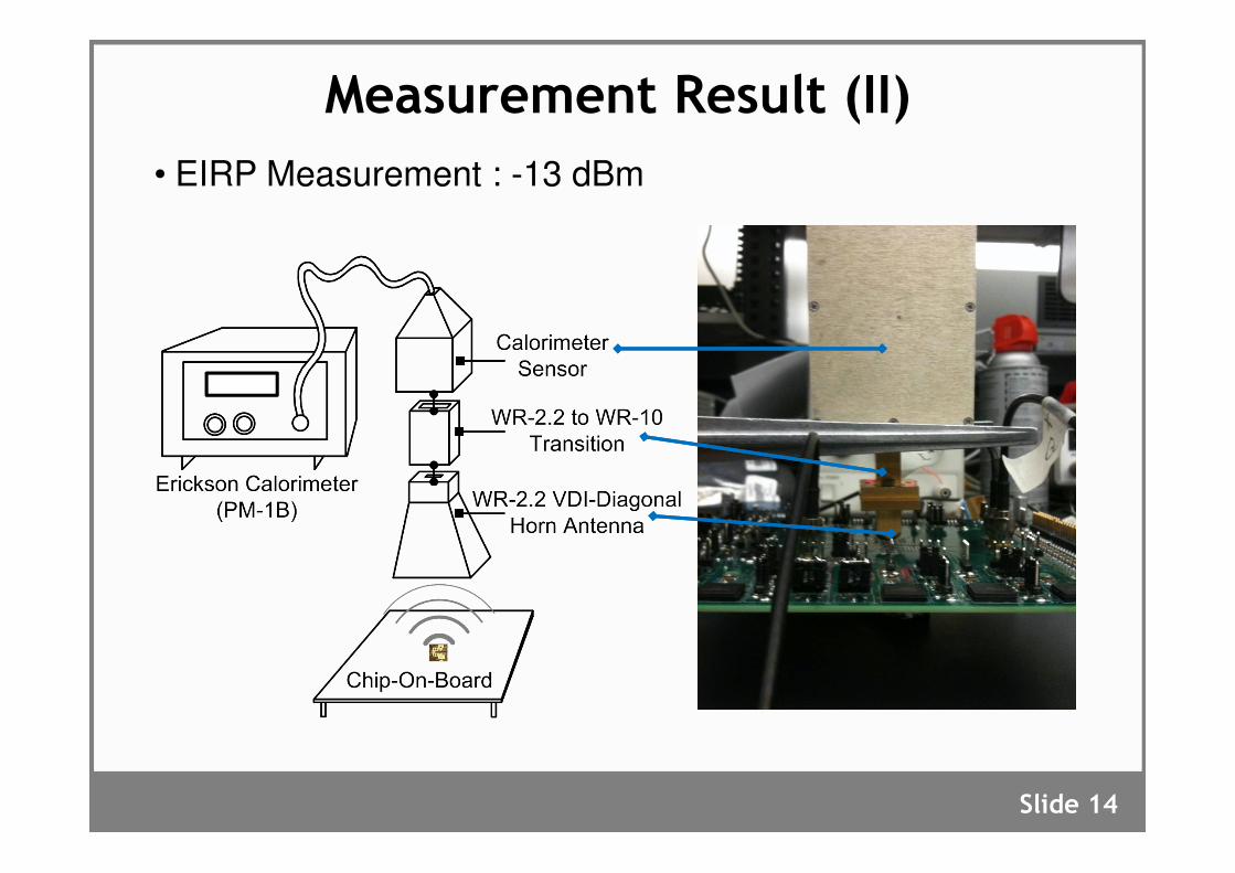
Measurement Result (II)
• EIRP Measurement : -13 dBm
Slide 14
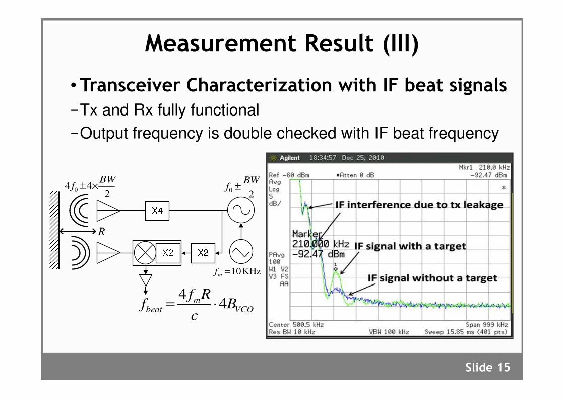
Measurement Result (III)
•Transceiver Characterization with IF beat signals
−Tx and Rx fully functional
−Output frequency is double checked with IF beat frequency
244 0
BWf ×±
20
BWf ±
KHz 10=mf
VCOm
beat Bc
Rff 4
4⋅=
R
Slide 15
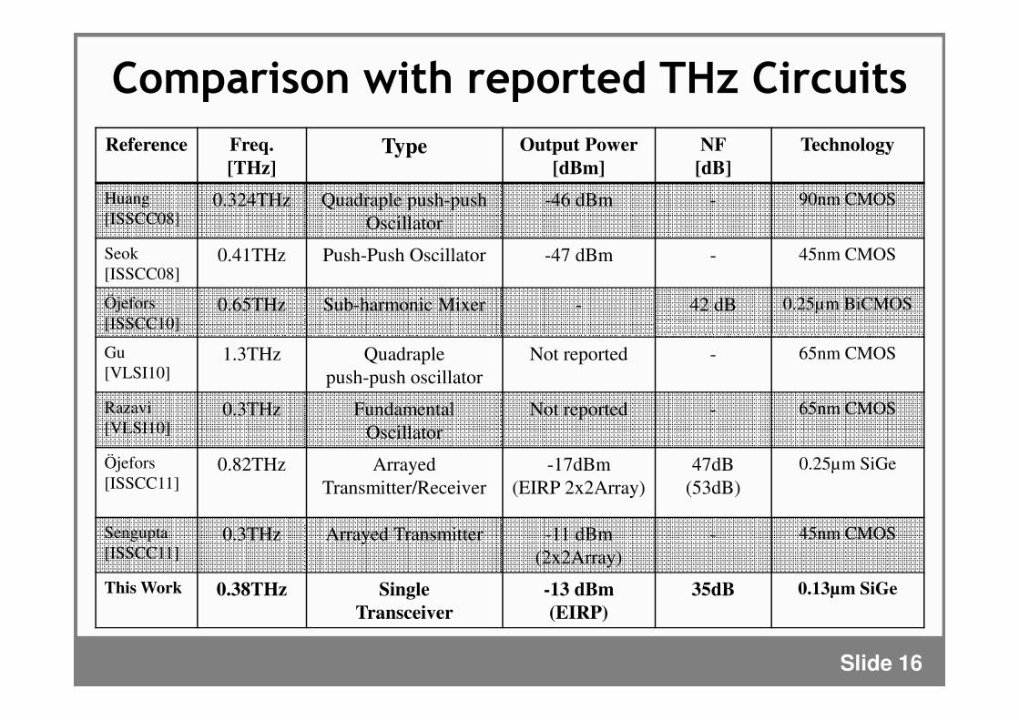
Comparison with reported THz Circuits
Reference Freq.
[THz]Type Output Power
[dBm]
NF
[dB]
Technology
Huang [ISSCC08]
0.324THz Quadraple push-push Oscillator
-46 dBm - 90nm CMOS
Seok [ISSCC08]
0.41THz Push-Push Oscillator -47 dBm - 45nm CMOS
Öjefors [ISSCC10]
0.65THz Sub-harmonic Mixer - 42 dB 0.25µm BiCMOS
Gu [VLSI10]
1.3THz Quadraple push-push oscillator
Not reported - 65nm CMOS
Razavi [VLSI10]
0.3THz Fundamental Oscillator
Not reported - 65nm CMOS
Öjefors [ISSCC11]
0.82THz Arrayed Transmitter/Receiver
-17dBm(EIRP 2x2Array)
47dB(53dB)
0.25µm SiGe
Sengupta [ISSCC11]
0.3THz Arrayed Transmitter -11 dBm (2x2Array)
- 45nm CMOS
This Work 0.38THz Single
Transceiver
-13 dBm
(EIRP)
35dB 0.13µm SiGe
Slide 16
WCA Futures SIG
Chip-to-Chip Communication
A “Wireless Bus”
J. Park, S. Kang, S. Thyagarajan,
E. Alon, A. Niknejad
Slide 17
Applications for very short range wireless
• If the bandwidth of a wireless bus is sufficiently high,
there are many interesting applications for such a
technology (chip-to-chip communication)
• Higher frequencies allow higher fractional bandwidths
and thus simple modulation schemes can be used to
realize high bandwidth links (50 Gbps).
• Higher frequencies (~300 GHz) also allow the on-chip
antennas to be smaller than pads, so there’s no extra
area overhead
• If the power consumption is ~ 0.5W, energy per bit is
about 10 pJ/bit, competitive with wired.
• Can it be done?
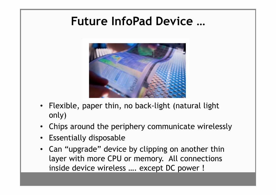
Future InfoPad Device …
• Flexible, paper thin, no back-light (natural light
only)
• Chips around the periphery communicate wirelessly
• Essentially disposable
• Can “upgrade” device by clipping on another thin
layer with more CPU or memory. All connections
inside device wireless …. except DC power !
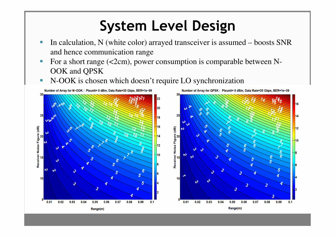
System Level Design� In calculation, N (white color) arrayed transceiver is assumed – boosts SNR
and hence communication range� For a short range (<2cm), power consumption is comparable between N-
OOK and QPSK� N-OOK is chosen which doesn’t require LO synchronization
Challenges
• Path loss at 240 GHz for ~1cm link is around ~36 dB – A reliable link requires high Equivalent Isotropically Radiated Power (EIRP)
• Requires design of efficient power amplifiers at mmwave frequencies to enhance EIRP
• Compared to conventional RF design, an LNA cannot be used at 240 GHz as it is beyond the fmax of the device – there is no power gain and very high noise figure
• Mixer design at 240 GHz needs to maximize the conversion gain with low noise figure. Elimination of LNA leads to very low available RF signal.
• IF Amplifier following the mixer at 60 GHz needs to provide high gain with high bandwidth to offset the effect of the LNA
• Testing requires design of on-chip PRBS at high data rates (~20 Gbps)
• Distribution of the data stream to the modulator blocks
Acknolodgement
• BWRC member companies
• Samsung Foundation
• NSF grant ECCS-0702037
• ST Microelectronics for chip donation
• NSF Infrastructure Grant No. 0403427
• “System IC2010” project of Korea Ministry of Knowledge Economy
Slide 22