Waveguide Basics - High-Speed Circuits & Systems Laboratory
23
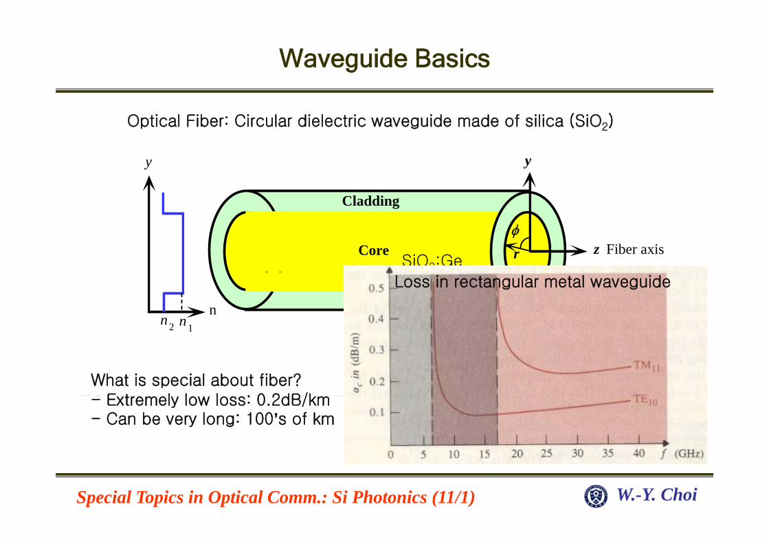
Waveguide Basics Optical Fiber: Circular dielectric waveguide made of silica (SiO 2 ) y Cladding y Core z r φ Fiber axis SiO 2 :Ge n n 2 n 1 Loss in rectangular metal waveguide What is special about fiber? Et l l l : 0 2dB/k use the coordinates r, φ , z to represent any point in the fiber. Cladding is normally much thicker than shown. ?1999 S.O. Kasap, Optoelectronics (Prentice Hall) - Extremely low loss: 0.2dB/km - Can be very long: 100’s of km Special Topics in Optical Comm.: Si Photonics (11/1) W.-Y. Choi
Transcript of Waveguide Basics - High-Speed Circuits & Systems Laboratory
Waveguide Basics
Optical Fiber: Circular dielectric waveguide made of silica (SiO2)
y
Cladding
y
Core zrφ
Fiber axisSiO2:Ge
nn2 n1
Loss in rectangular metal waveguide
The step index optical fiber. The central region, the core, has greater refractiveindex than the outer region, the cladding. The fiber has cylindrical symmetry. Weuse the coordinates r, φ, z to represent any point in the fiber. Cladding isWhat is special about fiber?
E t l l l : 0 2dB/kuse the coordinates r, φ, z to represent any point in the fiber. Cladding isnormally much thicker than shown.
?1999 S.O. Kasap, Optoelectronics (Prentice Hall)
- Extremely low loss: 0.2dB/km- Can be very long: 100’s of km
Special Topics in Optical Comm.: Si Photonics (11/1) W.-Y. Choi
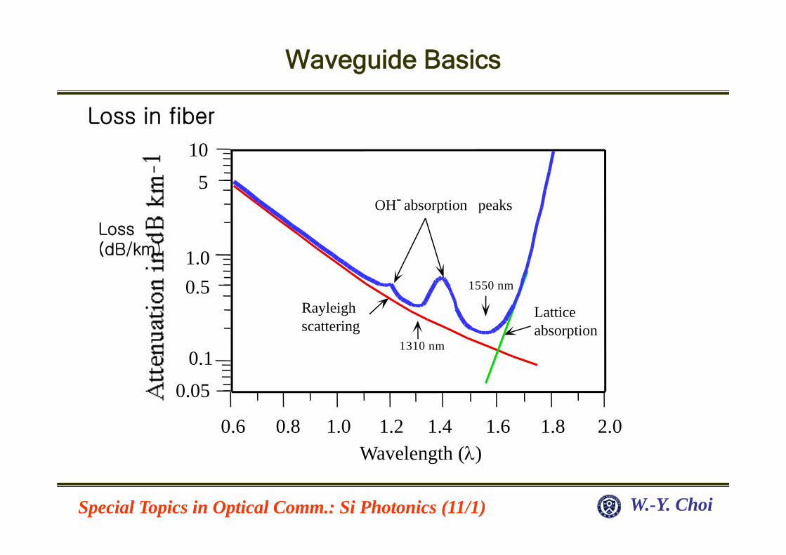
Waveguide Basics
Loss in fiber
10
5
10
OH- absorption peaks
1.0Loss(dB/km)
0.5Latticeabsorption
Rayleighscattering
1550 nm
0.05
0.11310 nm
0.6 0.8 1.0 1.2 1.4 1.6 1.8 2.0Wavelength (λ)
Special Topics in Optical Comm.: Si Photonics (11/1) W.-Y. Choi
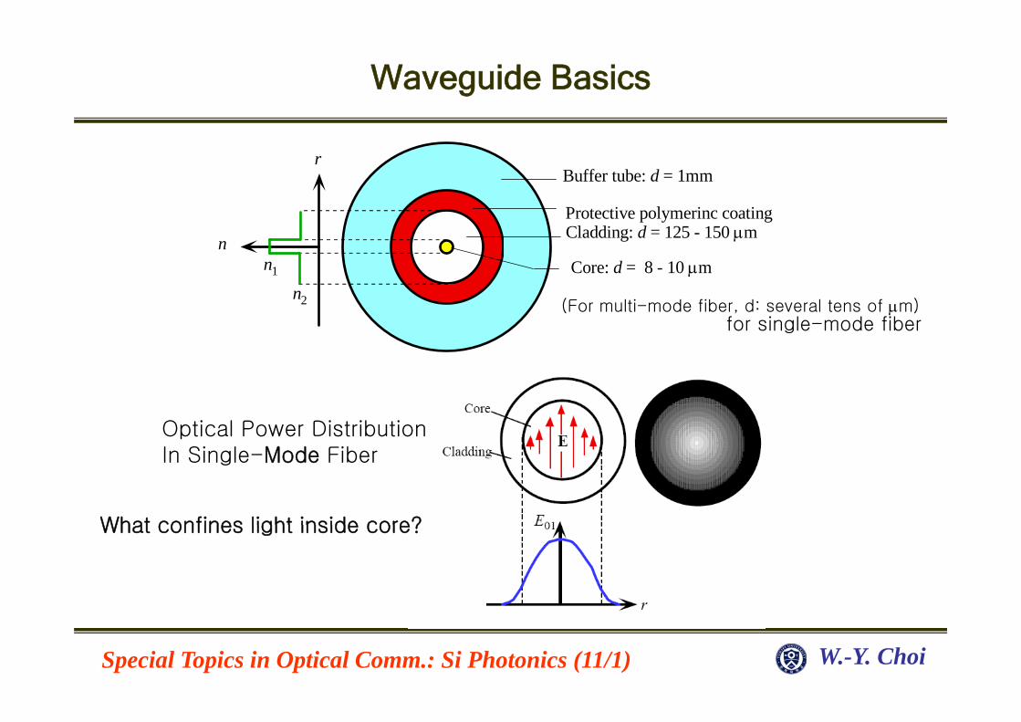
Waveguide Basics
Buffer tube: d = 1mmr
Protective polymerinc coatingCladding: d = 125 - 150 μm
Core: d = 8 - 10 μmn
n1
for single-mode fiber
n2 (For multi-mode fiber, d: several tens of μm)
The cross section of a typical single-mode fiber with a tight buffertube. (d = diameter)Optical Power Distribution
?1999 S.O. Kasap, Optoelectronics (Prentice Hall)In Single-Mode Fiber
What confines light inside core?What confines light inside core?
Special Topics in Optical Comm.: Si Photonics (11/1) W.-Y. Choi
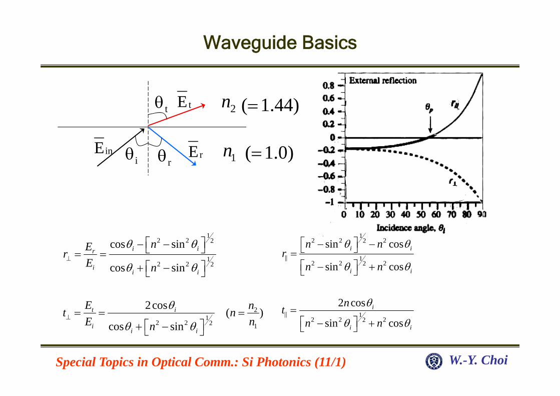
Waveguide Basics
tθ 2ntE ( 1 44)=
θ θ
t
n
2
inE E ( 1 0)=
( 1.44)=
iθ rθ 1ninE rE ( 1.0)=
12 2 2cos sinnE θ θ⎡ ⎤⎣ ⎦
12 2 22sin cosn nθ θ⎡ ⎤⎣ ⎦
12 2 2
cos sin
cos sin
i ir
ii i
nErE n
θ θ
θ θ⊥
⎡ ⎤− −⎣ ⎦= =⎡ ⎤+ −⎣ ⎦
|| 12 2 22
sin cos
sin cos
i i
i i
n nr
n n
θ θ
θ θ
⎡ ⎤− −⎣ ⎦=⎡ ⎤− +⎣ ⎦
21
2 2 2 1
2cos ( )cos sin
t i
ii i
E nt nE nn
θ
θ θ⊥ = = =
⎡ ⎤+ −⎣ ⎦
|| 12 2 22
2 cos
sin cosi
i i
ntn n
θ
θ θ=
⎡ ⎤− +⎣ ⎦
Special Topics in Optical Comm.: Si Photonics (11/1) W.-Y. Choi
i i⎣ ⎦
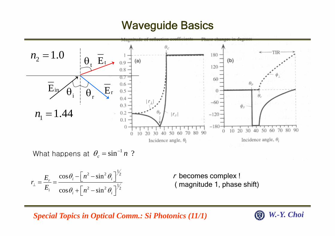
Waveguide Basics
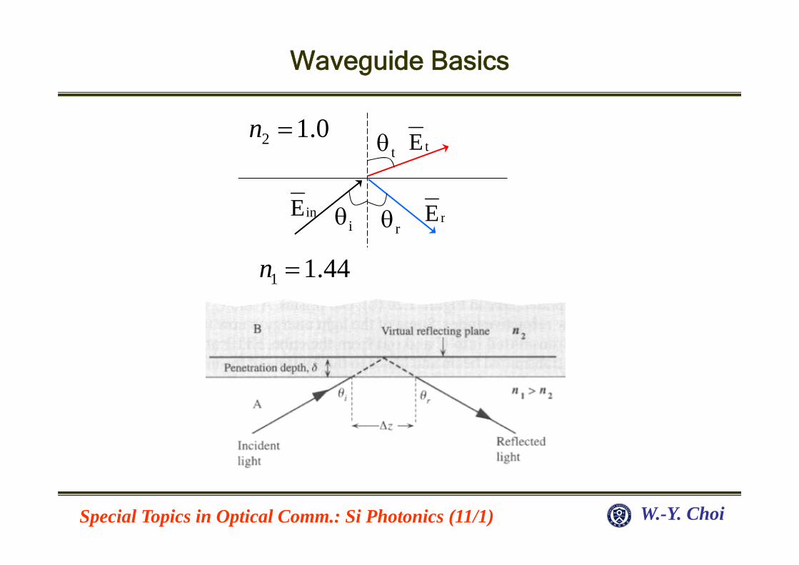
tθ2 1.0n =tE
θ θ
t
inE Eiθ rθ
1 1.44n =
inE rE
1
1⎡ ⎤
What happens at 1sin ?c nθ −=
12 2 2
12 2 2
cos sin
cos sin
i ir
ii i
nErE n
θ θ
θ θ⊥
⎡ ⎤− −⎣ ⎦= =⎡ ⎤+ −⎣ ⎦
r becomes complex !( magnitude 1, phase shift)
Special Topics in Optical Comm.: Si Photonics (11/1) W.-Y. Choi
Waveguide Basics
tθ2 1.0n =tE
θ θ
t
inE rEiθ rθ
1 1.44n =
rE
1
Special Topics in Optical Comm.: Si Photonics (11/1) W.-Y. Choi
Waveguide Basics
d
n2
0
y=d/2
y
z3 l di l t i uid d n1
n2
y=0
y=-d/2
z3-layer dielectric waveguide
Full analysis starting from wave equations.
22
2( , , ) ( , , )EE y z t y z tμε ∂∇ =
∂ 2( , , ) ( , , )y yt
μ∂
( ) ( )Assuming , , , , j tE y z t E y z e ω= ⋅
2 2 2 2( ) 0 h ( ) ( )k k
( ) for y ; claddingdk y n k= >
2 2 2 2( ) 0, where ( ) ( )E k y E k y yμε ω∇ + = =
2 0
1 0
( ) for y ; cladding2
( ) for y ; core2
k y n k
dk y n k
= >
= <
Special Topics in Optical Comm.: Si Photonics (11/1) W.-Y. Choi
1 0( ) y2
y
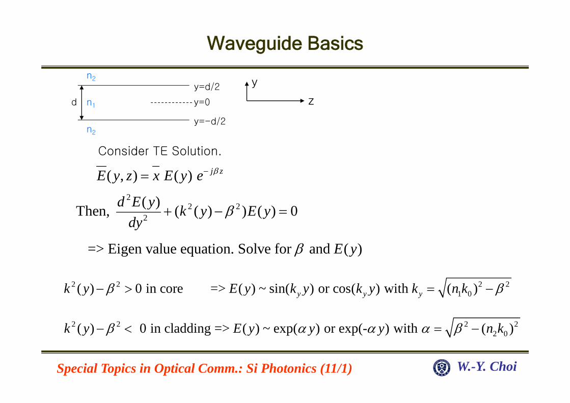
Waveguide Basics
d
n2
n1 y=0
y=d/2 y
z
Consider TE Solution.
n2
y=-d/2
( , ) ( ) j zE y z x E y e β−=2 ( )d E y 2 2
2
( )Then, ( ( ) ) ( ) 0d E y k y E ydy
β+ − =
=> Eigen value equation Solve for and ( )E yβ
2 2 2 21 0 ( ) 0 in core => ( ) ~ sin( ) or cos( ) with ( )y y yk y E y k y k y k n kβ β− > = −
=> Eigen value equation. Solve for and ( )E yβ
1 0( ) ( ) ( ) ( ) ( )y y yy y y yβ β
2 2 2 22 0( ) 0 in cladding => ( ) ~ exp( ) or exp(- ) with ( )k y E y y y n kβ α α α β− < = −
Special Topics in Optical Comm.: Si Photonics (11/1) W.-Y. Choi
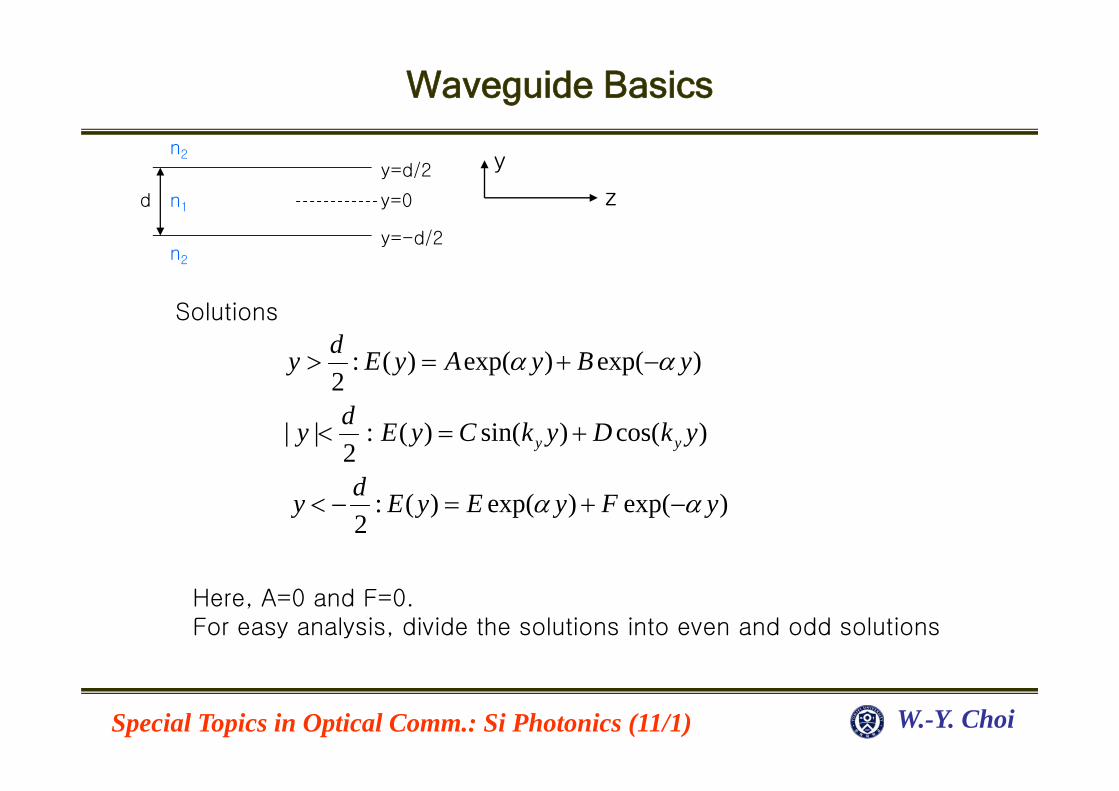
Waveguide Basics
d
n2
n1 y=0
y=d/2 y
z
n2
y=-d/2
S l tiSolutions
: ( ) exp( ) exp( )2dy E y A y B yα α> = + −
| | : ( ) sin( ) cos( )2 y ydy E y C k y D k y
d
< = +
: ( ) exp( ) exp( )2dy E y E y F yα α< − = + −
Here, A=0 and F=0.For easy analysis, divide the solutions into even and odd solutions
Special Topics in Optical Comm.: Si Photonics (11/1) W.-Y. Choi
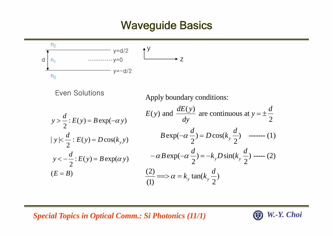
Waveguide Basics
d
n2
n1 y=0
y=d/2 y
z
n2
y=-d/2
E S l tiEven Solutions Apply boundary conditions:( )( ) and are continuous at
2dE y dE y y
d= ±
( ) ( )d E B 2
exp( ) cos( ) ------- (1)2 2y
dyd dB D kα− =
: ( ) exp( )2
| | : ( ) cos( )2 y
dy E y B y
dy E y D k y
α> = −
< =
exp( ) sin( ) ----- (2)2 2
(2)
y yd dB k D k
d
α α− − = −2
: ( ) exp( )2
( )
dy E y B y
E B
α< − =
(2) tan( )(1) 2y y
dk kα==> =( )E B=
Special Topics in Optical Comm.: Si Photonics (11/1) W.-Y. Choi
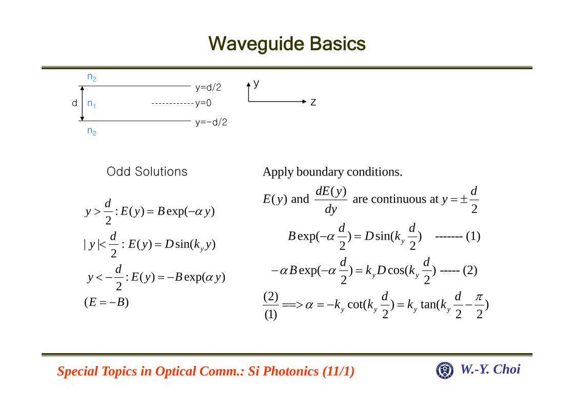
Waveguide Basics
d
n2
n1 y=0
y=d/2 y
z
n2
y=-d/2
Odd Solutions Apply boundary conditions.( )( ) and are continuous at dE y dE y y = ±d ( ) d e co uous
2
exp( ) sin( ) ------- (1)2 2y
y ydy
d dB D kα− =
: ( ) exp( )2
| | : ( ) sin( )2 y
dy E y B y
dy E y D k y
α> = −
< = 2 2
exp( ) cos( ) ----- (2)2 2
(2)
y yd dB k D k
d d
α α
π
− − =
| | ( ) ( )2
: ( ) exp( )2
yy y y
dy E y B yα< − = −
(2) cot( ) tan( )(1) 2 2 2y y y y
d dk k k k πα==> = − = −( )E B= −
Special Topics in Optical Comm.: Si Photonics (11/1) W.-Y. Choi
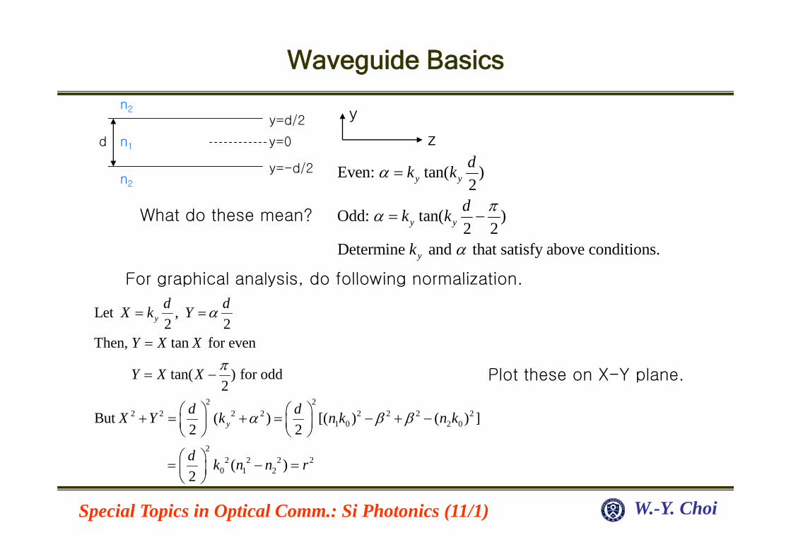
Waveguide Basics
d
n2
n1 y=0
y=d/2 y
z
n2
y=-d/2
What do these mean?
Even: tan( )2
Odd: tan( )
y ydk k
dk k
α
πα
=
=What do these mean? Odd: tan( )2 2
Determine and that satisfy above conditions.
y y
y
k k
k
α
α
= −
For graphical analysis do following normalizationFor graphical analysis, do following normalization.
Let ,2 2
Then tan for even
yd dX k Y
Y X X
α= =
=
2 2
Then, tan for even
tan( ) for odd2
Y X X
Y X X
d d
π=
= −
⎛ ⎞ ⎛ ⎞
Plot these on X-Y plane.
2 2 2 2 2 2 2 21 0 2 0
22 2 2 2
0 1 2
But ( ) [( ) ( ) ]2 2
( )
yd dX Y k n k n k
d k n n r
α β β⎛ ⎞ ⎛ ⎞+ = + = − + −⎜ ⎟ ⎜ ⎟⎝ ⎠ ⎝ ⎠
⎛ ⎞= − =⎜ ⎟⎝ ⎠
Special Topics in Optical Comm.: Si Photonics (11/1) W.-Y. Choi
0 1 2( )2⎜ ⎟
⎝ ⎠
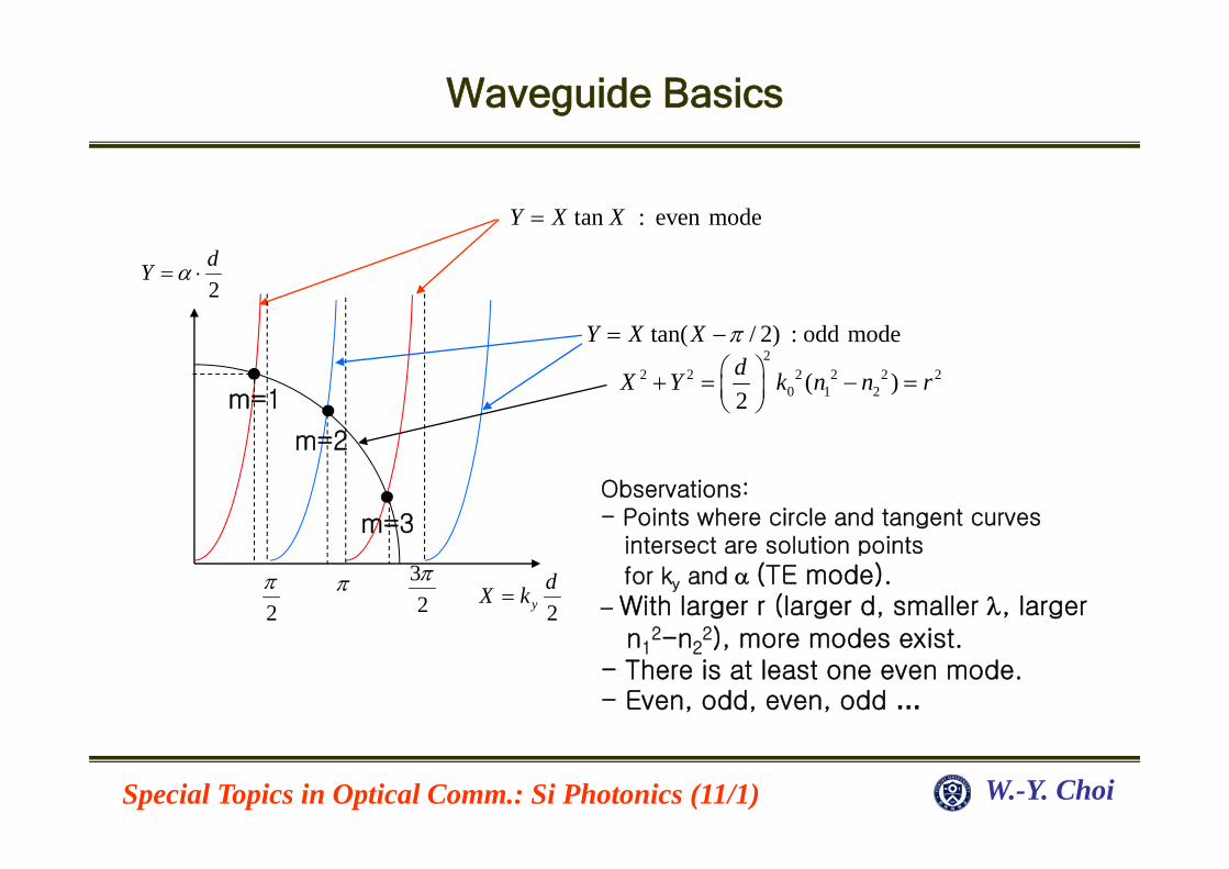
Waveguide Basics
tan : even modeY X X=
tan( / 2) : odd modeY X X π= −
2dY α= ⋅
tan( / 2) : odd modeY X X π= −2
2 2 2 2 2 20 1 2( )
2dX Y k n n r⎛ ⎞+ = − =⎜ ⎟
⎝ ⎠m=1
2
Observations:- Points where circle and tangent curvesm=3
m=2
2ydX k=
2π π 3
2π
intersect are solution points
for ky and α (TE mode).− With larger r (larger d, smaller λ, larger
2 2) d i tn12-n2
2), more modes exist.- There is at least one even mode.- Even, odd, even, odd …
Special Topics in Optical Comm.: Si Photonics (11/1) W.-Y. Choi
Waveguide Basics
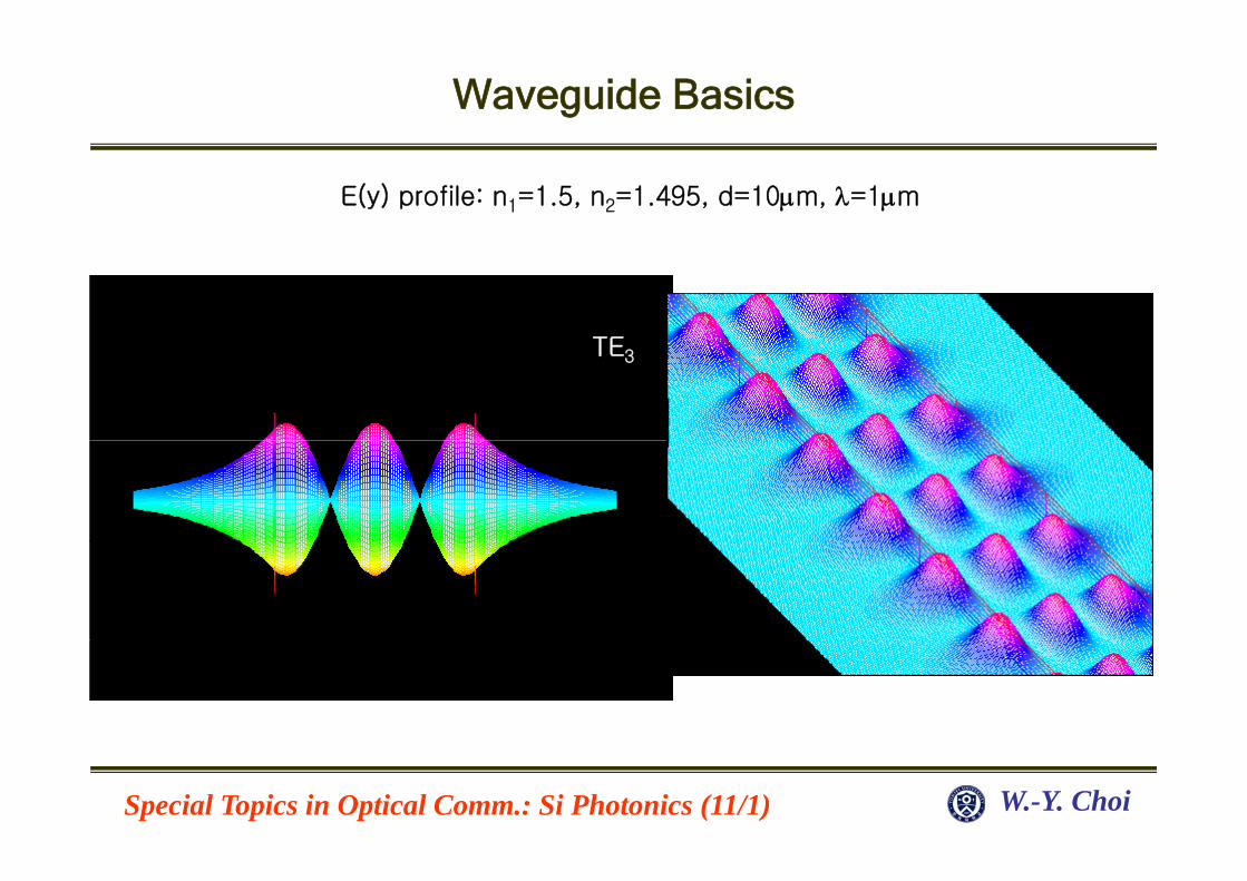
E(y) profile: n1=1.5, n2=1.495, d=10μm, λ=1μm
TE1 TETE1 TE2TE3
Special Topics in Optical Comm.: Si Photonics (11/1) W.-Y. Choi
Waveguide Basics
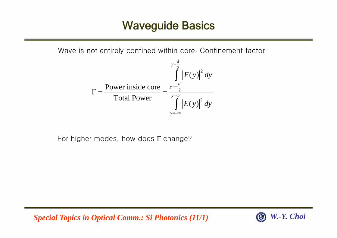
Wave is not entirely confined within core: Confinement factor
dy=2
2
2
( )Power inside core
y
dy
E y dy=−
Γ = =
∫
2Total Power( )
y
y
E y dy=∞
=−∞
Γ = =
∫
For higher modes, how does Γ change?
Special Topics in Optical Comm.: Si Photonics (11/1) W.-Y. Choi
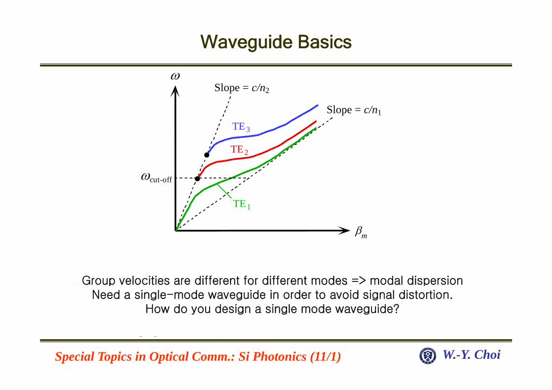
Waveguide Basics
ωSlope = c/n2
Sl /Slope = c/n1
TE2
TE3
ωcut-off
TE2
βm
TE1
Schematic dispersion diagram, ω vs. β for the slab waveguide for various TE m. modes.ωcut–off corresponds to V = π/2. The group velocity vg at any ω is the slope of the ω vs. βGroup velocities are different for different modes => modal dispersioncut off p g p y g y p βcurve at that frequency.
© 1999 S O K O l i (P i H ll)
Group velocities are different for different modes > modal dispersionNeed a single-mode waveguide in order to avoid signal distortion.
How do you design a single mode waveguide?
Special Topics in Optical Comm.: Si Photonics (11/1) W.-Y. Choi
© 1999 S.O. Kasap, Optoelectronics (Prentice Hall)
Waveguide Basics
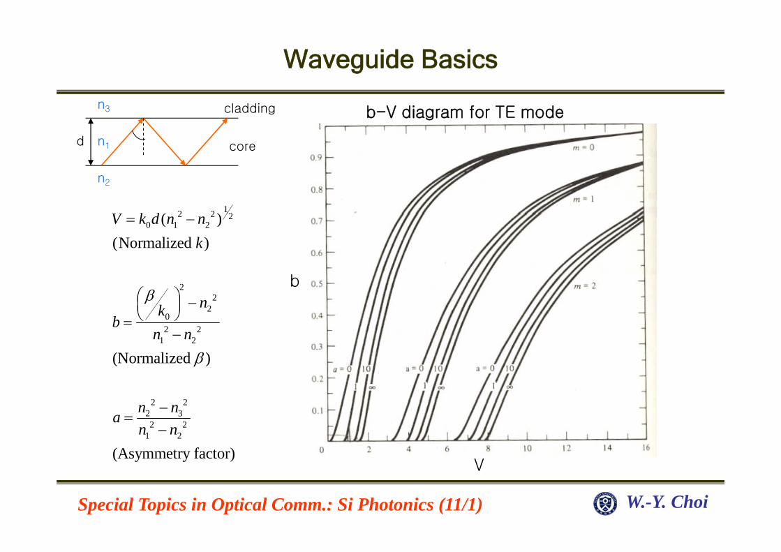
b-V diagram for TE mode
d
n3
n1 core
cladding
12 2 2( )k d
co e
n2
b
2 2 20 1 2( )
(Normalized )V k d n n
k= −
b22
202 2
1 2
nkb
n n
β⎛ ⎞ −⎜ ⎟⎝ ⎠=
−1 2
2 2
(Normalized )n n
β
V
2 22 32 2
1 2
(Asymmetry factor)
n nan n
−=
−
Special Topics in Optical Comm.: Si Photonics (11/1) W.-Y. Choi
V
Waveguide Basics
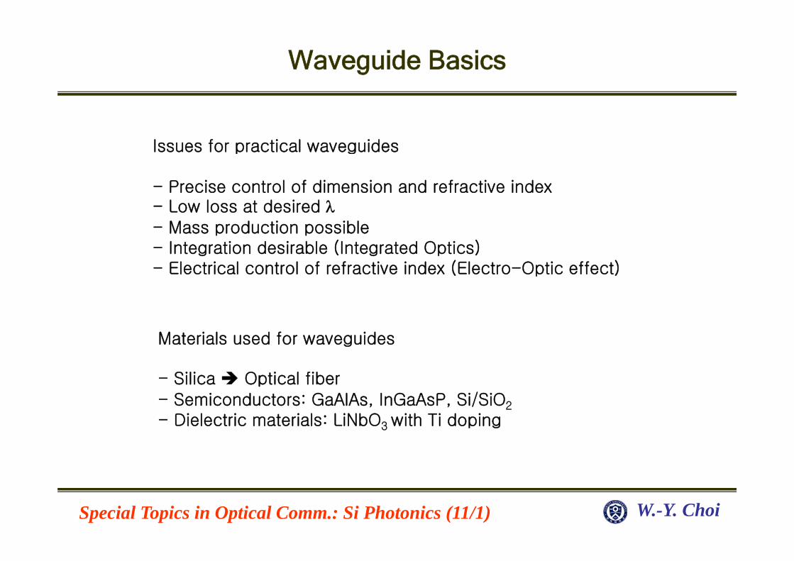
Issues for practical waveguidesp g
- Precise control of dimension and refractive index - Low loss at desired λ- Mass production possible- Integration desirable (Integrated Optics)- Electrical control of refractive index (Electro-Optic effect)
Materials used for waveguidesMaterials used for waveguides
- Silica Optical fiber- Semiconductors: GaAlAs, InGaAsP, Si/SiO22
- Dielectric materials: LiNbO3 with Ti doping
Special Topics in Optical Comm.: Si Photonics (11/1) W.-Y. Choi
Waveguide Basics
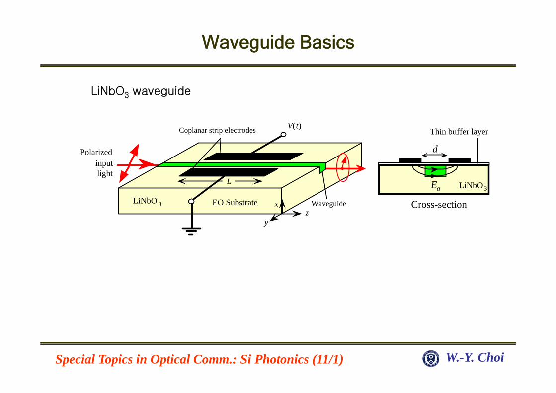
LiNbO3 waveguide
V(t)
d
Thin buffer layerCoplanar strip electrodes
Polarized
Ea LiNbO3
dPolarizedinputlight
L
Cross-sectionEO Substratez
y
x WaveguideLiNbO 3
Integrated tranverse Pockels cell phase modulator in which a waveguide is diffusedinto an electro-optic (EO) substrate. Coplanar strip electrodes apply a transversefield Ea through the waveguide. The substrate is an x-cut LiNbO3 and typically thereis a thin dielectric buffer layer (e.g. ~200 nm thick SiO2) between the surfaceelectrodes and the substrate to separate the electrodes away from the waveguide.?1999 S.O. Kasap, Optoelectronics (Prentice Hall)
Special Topics in Optical Comm.: Si Photonics (11/1) W.-Y. Choi
p, p ( )
Waveguide Basics
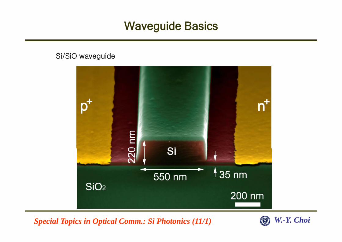
Si/SiO waveguide
Special Topics in Optical Comm.: Si Photonics (11/1) W.-Y. Choi
Waveguide Basics
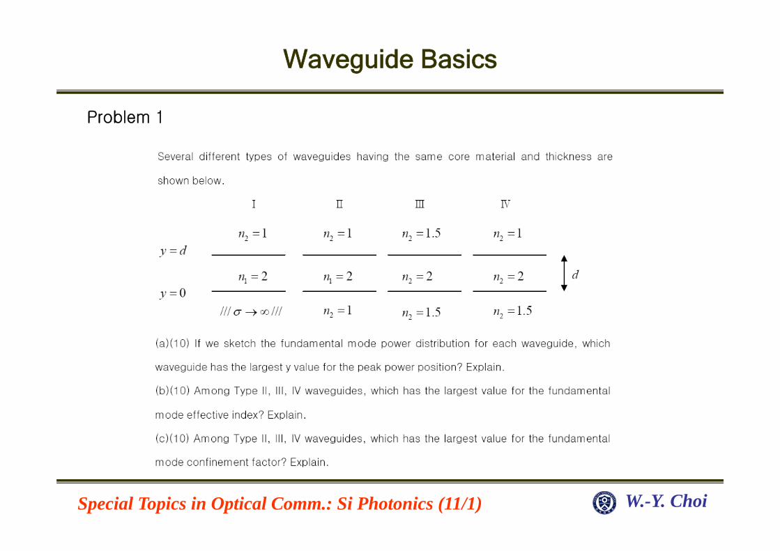
Problem 1
Special Topics in Optical Comm.: Si Photonics (11/1) W.-Y. Choi
Waveguide Basics
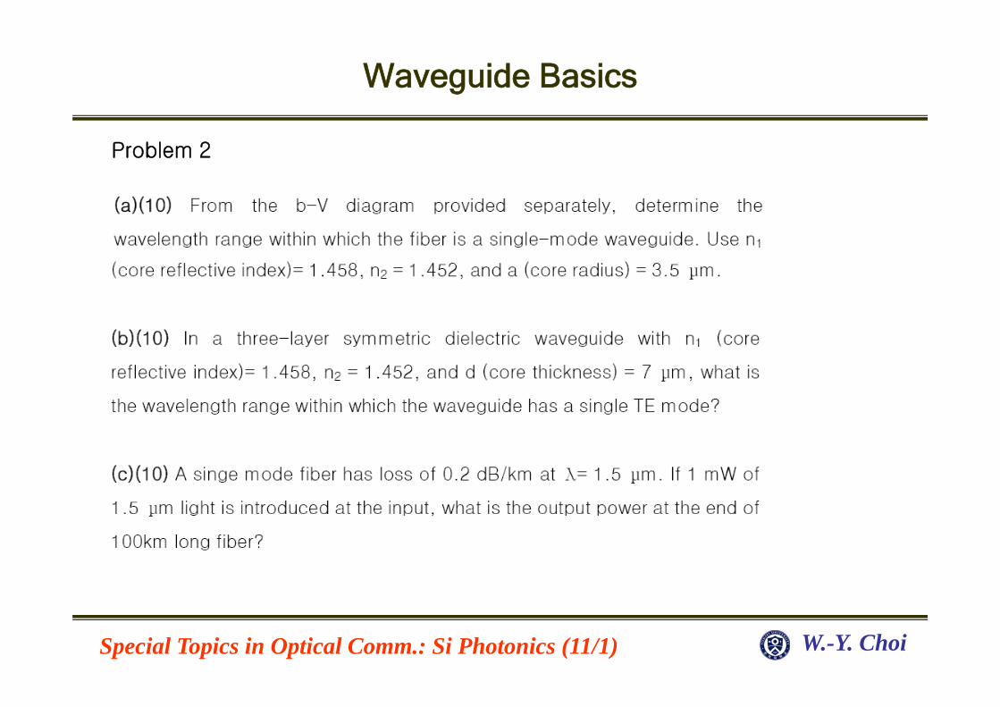
Problem 2
Special Topics in Optical Comm.: Si Photonics (11/1) W.-Y. Choi
Waveguide Basics
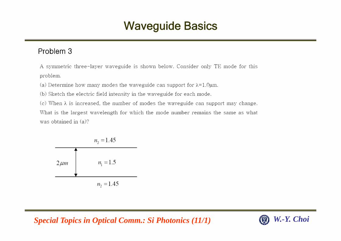
Problem 3
Special Topics in Optical Comm.: Si Photonics (11/1) W.-Y. Choi