
UMBC 1 (Nov. 19, 2001) - UNM
21
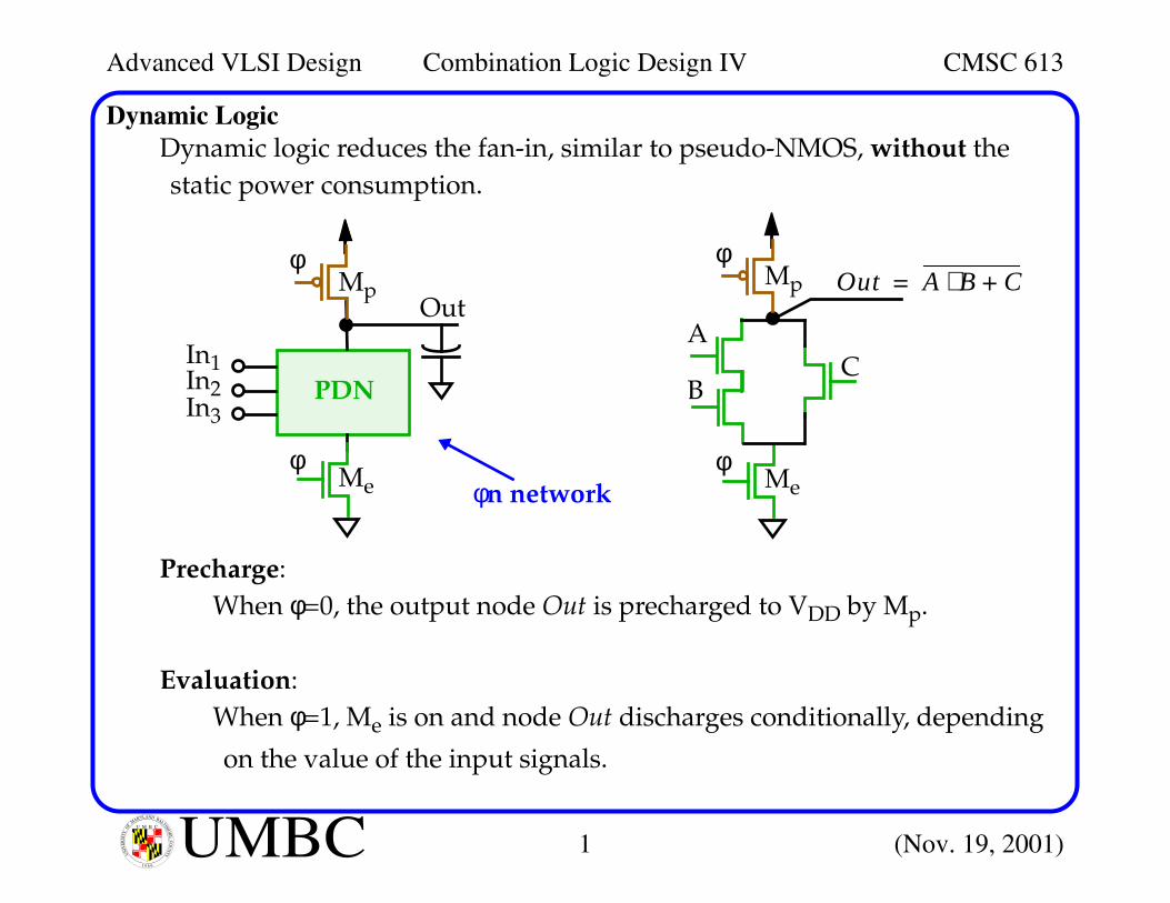
Advanced VLSI Design Combination Logic Design IV CMSC 613 1 (Nov. 19, 2001) UMBC U M B C UN IV E R S IT Y O F M A R Y L A N D B A L T I M O R E C O U N T Y 1 9 6 6 Dynamic Logic Dynamic logic reduces the fan-in, similar to pseudo-NMOS, without the static power consumption. Precharge: When φ=0, the output node Out is precharged to V DD by M p . Evaluation: When φ=1, M e is on and node Out discharges conditionally, depending on the value of the input signals. PDN In 1 In 2 In 3 Out φ φ M e M p φn network φ φ M e M p A B C Out A B ⋅ C + =
Transcript of UMBC 1 (Nov. 19, 2001) - UNM
Advanced VLSI Design Combination Logic Design IV CMSC 613
1 (Nov. 19, 2001)UMBCU M B C
UN
IVE
RSI
TY
OF
MARYLAND BALTIM
OR
E C
OU
NTY
1 9 6 6
Dynamic LogicDynamic logic reduces the fan-in, similar to pseudo-NMOS, without thestatic power consumption.
Precharge:When φ=0, the output node Out is precharged to VDD by Mp.
Evaluation:When φ=1, Me is on and node Out discharges conditionally, depending
on the value of the input signals.
PDNIn1In2In3
Out
φ
φMe
Mp
φn network
φ
φMe
Mp
A
BC
Out A B⋅ C+=
Advanced VLSI Design Combination Logic Design IV CMSC 613
2 (Nov. 19, 2001)UMBCU M B C
UN
IVE
RSI
TY
OF
MARYLAND BALTIM
OR
E C
OU
NTY
1 9 6 6
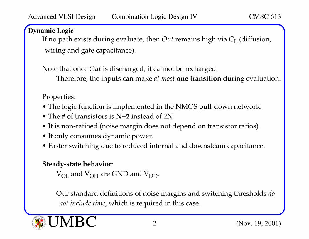
Dynamic LogicIf no path exists during evaluate, then Out remains high via CL (diffusion,
wiring and gate capacitance).
Note that once Out is discharged, it cannot be recharged.Therefore, the inputs can make at most one transition during evaluation.
Properties:• The logic function is implemented in the NMOS pull-down network.• The # of transistors is N+2 instead of 2N• It is non-ratioed (noise margin does not depend on transistor ratios).• It only consumes dynamic power.• Faster switching due to reduced internal and downsteam capacitance.
Steady-state behavior:VOL and VOH are GND and VDD.
Our standard definitions of noise margins and switching thresholds donot include time, which is required in this case.
Advanced VLSI Design Combination Logic Design IV CMSC 613
3 (Nov. 19, 2001)UMBCU M B C
UN
IVE
RSI
TY
OF
MARYLAND BALTIM
OR
E C
OU
NTY
1 9 6 6
Dynamic LogicSteady-state behavior (cont):
For example, noise margins depend on the length of the evaluate.If clk is too long, leakage affects the high output level significantly.
Since the pull down network starts to conduct when the input signalexceeds VTn, it is reasonable to set VM, VIH, VIL = VTn.
Therefore, NML is very low.
Note that this is a conservative estimate since subthreshold leakage occursfor inputs below VTn.
Also note that the high output level is sensitive to noise and couplingdisturbances because of its high output impedance.
The high value of NMH compensates for this increased sensitivity.
Advanced VLSI Design Combination Logic Design IV CMSC 613
4 (Nov. 19, 2001)UMBCU M B C
UN
IVE
RSI
TY
OF
MARYLAND BALTIM
OR
E C
OU
NTY
1 9 6 6
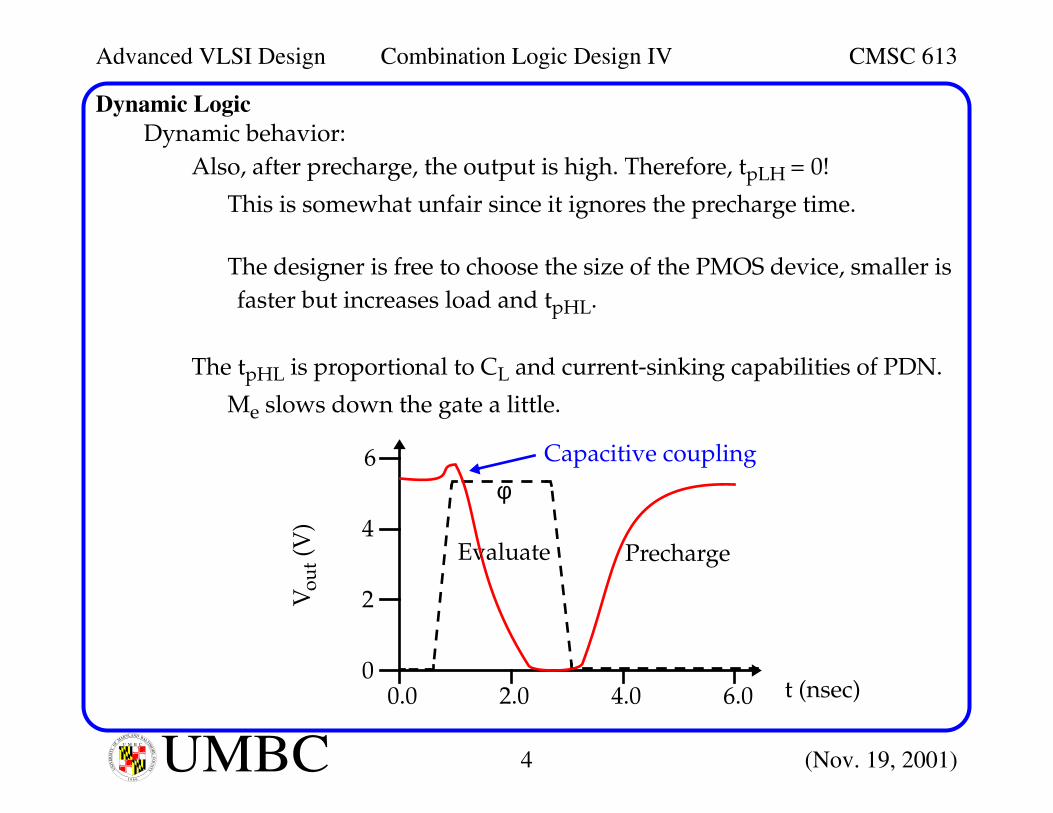
Dynamic LogicDynamic behavior:
Also, after precharge, the output is high. Therefore, tpLH = 0!
This is somewhat unfair since it ignores the precharge time.
The designer is free to choose the size of the PMOS device, smaller isfaster but increases load and tpHL.
The tpHL is proportional to CL and current-sinking capabilities of PDN.
Me slows down the gate a little.
0.00
2
4
6
Vou
t (V
)
2.0 4.0 6.0 t (nsec)
φCapacitive coupling
PrechargeEvaluate
Advanced VLSI Design Combination Logic Design IV CMSC 613
5 (Nov. 19, 2001)UMBCU M B C
UN
IVE
RSI
TY
OF
MARYLAND BALTIM
OR
E C
OU
NTY
1 9 6 6
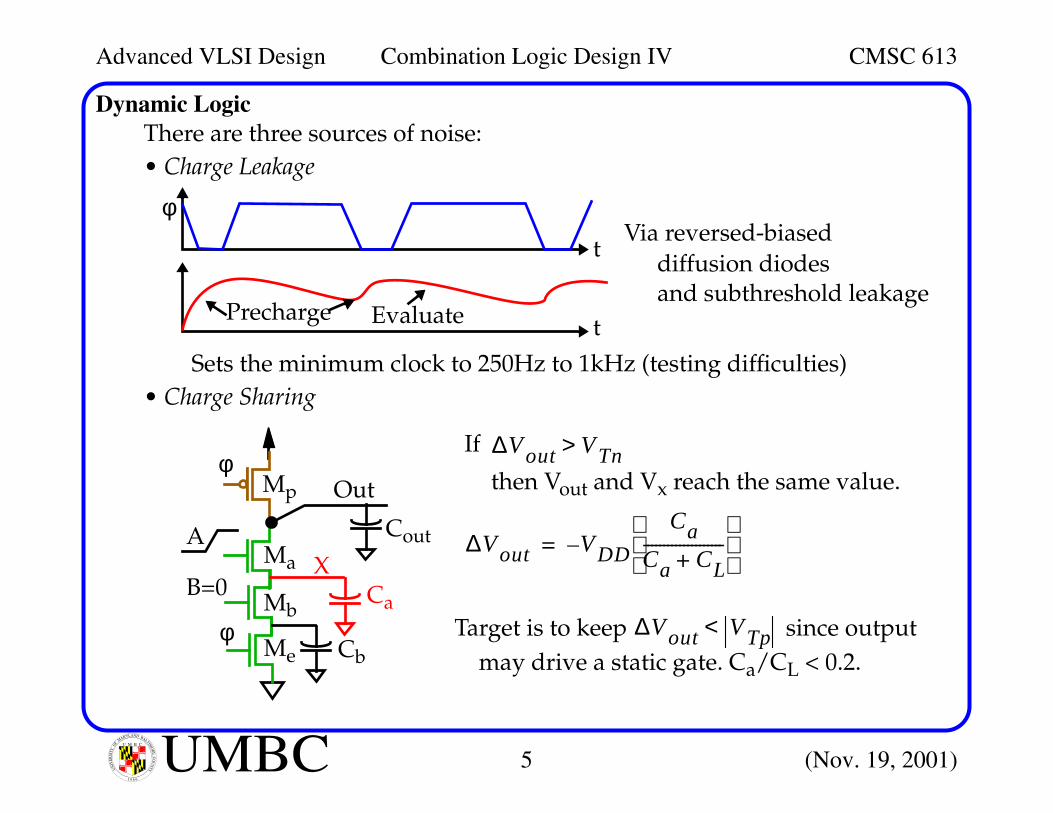
Dynamic LogicThere are three sources of noise:• Charge Leakage
Sets the minimum clock to 250Hz to 1kHz (testing difficulties)• Charge Sharing
t
φ
Precharge Evaluate
tVia reversed-biased
diffusion diodesand subthreshold leakage
φ
φMe
Mp
A
B=0
Out
Mb
Ma
Ca
Cb
Cout ∆Vout V DD–Ca
Ca CL+--------------------
=
∆Vout VTn>If
then Vout and Vx reach the same value.
X
Target is to keep ∆Vout VTp< since outputmay drive a static gate. Ca/CL < 0.2.
Advanced VLSI Design Combination Logic Design IV CMSC 613
6 (Nov. 19, 2001)UMBCU M B C
UN
IVE
RSI
TY
OF
MARYLAND BALTIM
OR
E C
OU
NTY
1 9 6 6
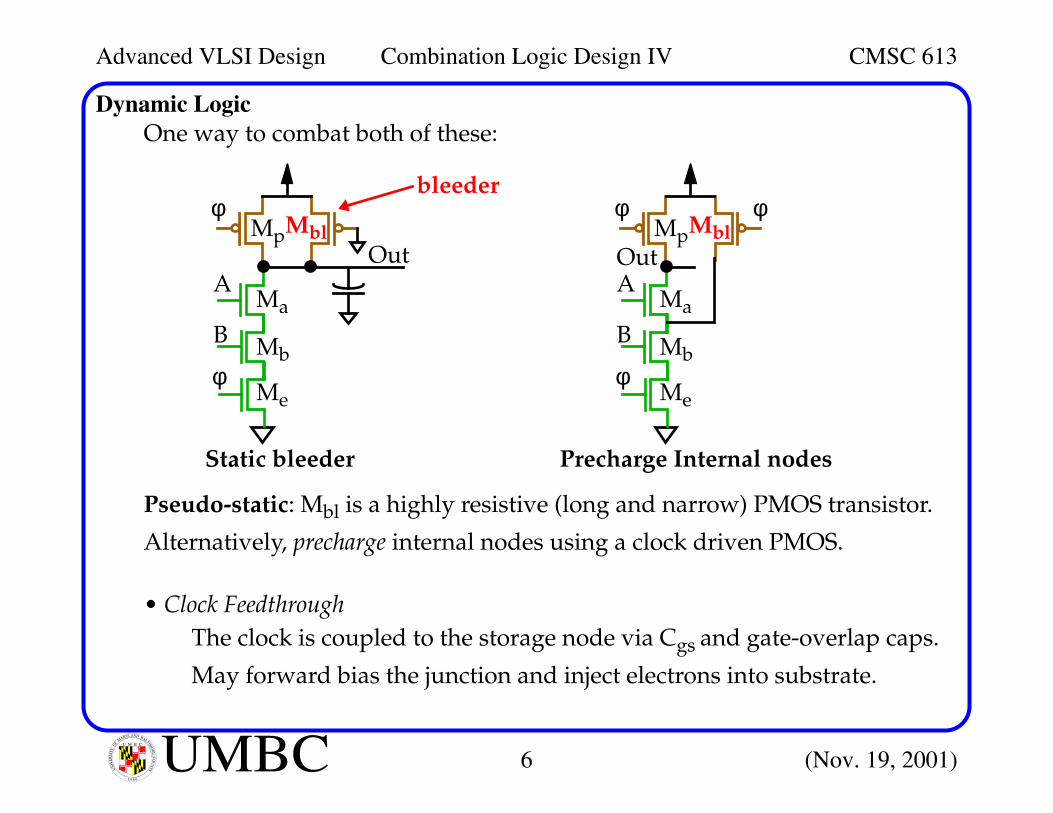
Dynamic LogicOne way to combat both of these:
Pseudo-static: Mbl is a highly resistive (long and narrow) PMOS transistor.
Alternatively, precharge internal nodes using a clock driven PMOS.
• Clock FeedthroughThe clock is coupled to the storage node via Cgs and gate-overlap caps.
May forward bias the junction and inject electrons into substrate.
φ
φMe
Mp
A
B
Out
Mb
Ma
Mbl
bleeder
Static bleeder
φ
φMe
Mp
A
B
Out
Mb
Ma
Mbl
Precharge Internal nodes
φ
Advanced VLSI Design Combination Logic Design IV CMSC 613
7 (Nov. 19, 2001)UMBCU M B C
UN
IVE
RSI
TY
OF
MARYLAND BALTIM
OR
E C
OU
NTY
1 9 6 6
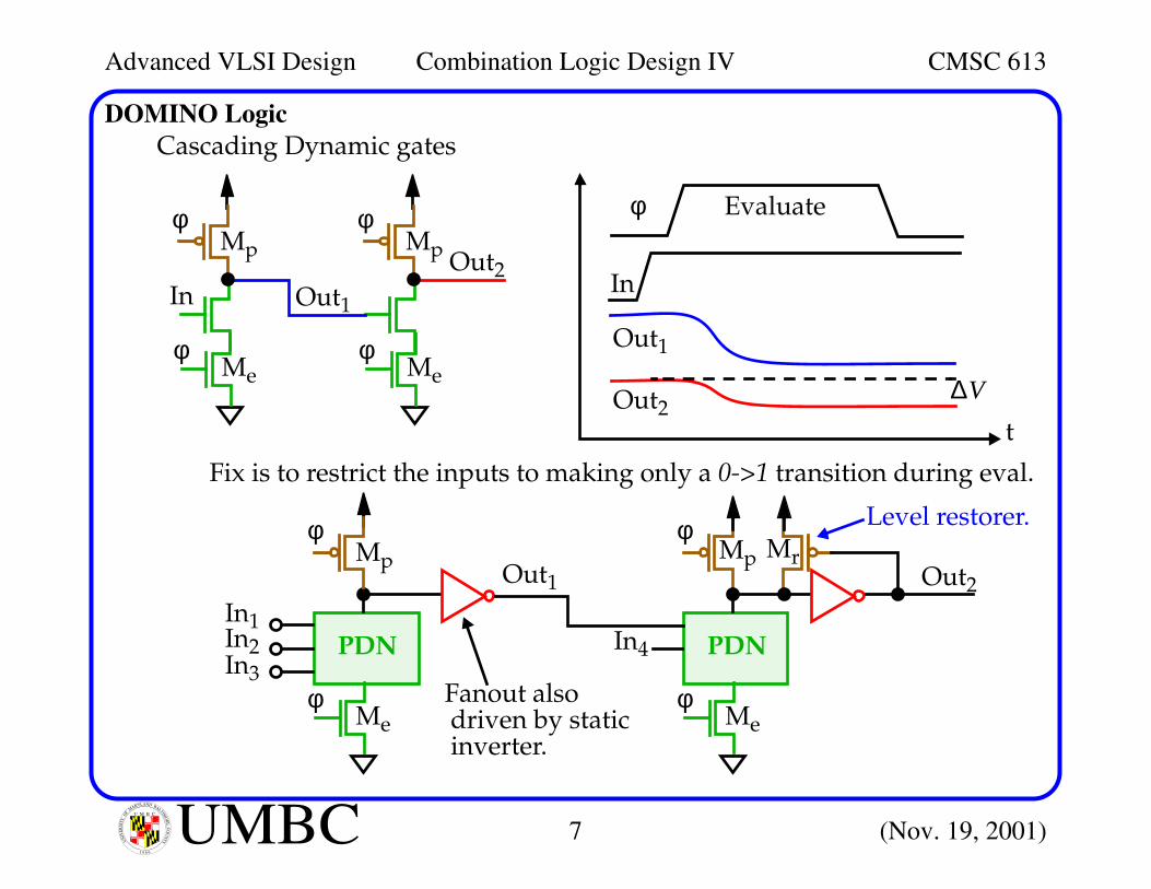
DOMINO LogicCascading Dynamic gates
Fix is to restrict the inputs to making only a 0->1 transition during eval.
φ
φMe
Mp
In
φ
φMe
Mp
Out1
Out2
φ Evaluate
In
Out1
Out2∆V
t
PDNIn1In2In3
Out1
φ
φMe
Mp
PDNIn4
φ
φMe
MpOut2
Mr
Fanout alsodriven by staticinverter.
Level restorer.
Advanced VLSI Design Combination Logic Design IV CMSC 613
8 (Nov. 19, 2001)UMBCU M B C
UN
IVE
RSI
TY
OF
MARYLAND BALTIM
OR
E C
OU
NTY
1 9 6 6
DOMINO LogicDuring evaluation, either the output of the first DOMINO stays at 0 (nodelay!) or makes a 0->1 transition.
The transition may ripple all the way down the chain.
Properties:• Only non-inverting logic can be implemented.• Appropriate for complex, large fan-out circuits such as ALUs or control cir-
cuits.• Very high speeds can be achieved, tpHL = 0.
In the past, DOMINO was used in the design of a number of high speed ICs.The first 32-bit microprocessor (BellMAC 32) used it.
Recently, pure DOMINO circuits are rare, mainly due to the non-invertinglogic property.
Advanced VLSI Design Combination Logic Design IV CMSC 613
9 (Nov. 19, 2001)UMBCU M B C
UN
IVE
RSI
TY
OF
MARYLAND BALTIM
OR
E C
OU
NTY
1 9 6 6
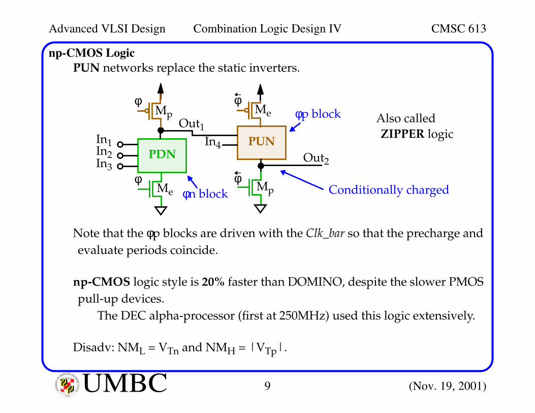
np-CMOS LogicPUN networks replace the static inverters.
Note that the φp blocks are driven with the Clk_bar so that the precharge andevaluate periods coincide.
np-CMOS logic style is 20% faster than DOMINO, despite the slower PMOSpull-up devices.
The DEC alpha-processor (first at 250MHz) used this logic extensively.
Disadv: NML = VTn and NMH = |VTp|.
PDNIn1In2In3
Out1
φ
φMe
Mp
PUNIn4
φ
φMp
Me
Out2
φp block
φn block
Also calledZIPPER logic
Conditionally charged
Advanced VLSI Design Combination Logic Design IV CMSC 613
10 (Nov. 19, 2001)UMBCU M B C
UN
IVE
RSI
TY
OF
MARYLAND BALTIM
OR
E C
OU
NTY
1 9 6 6
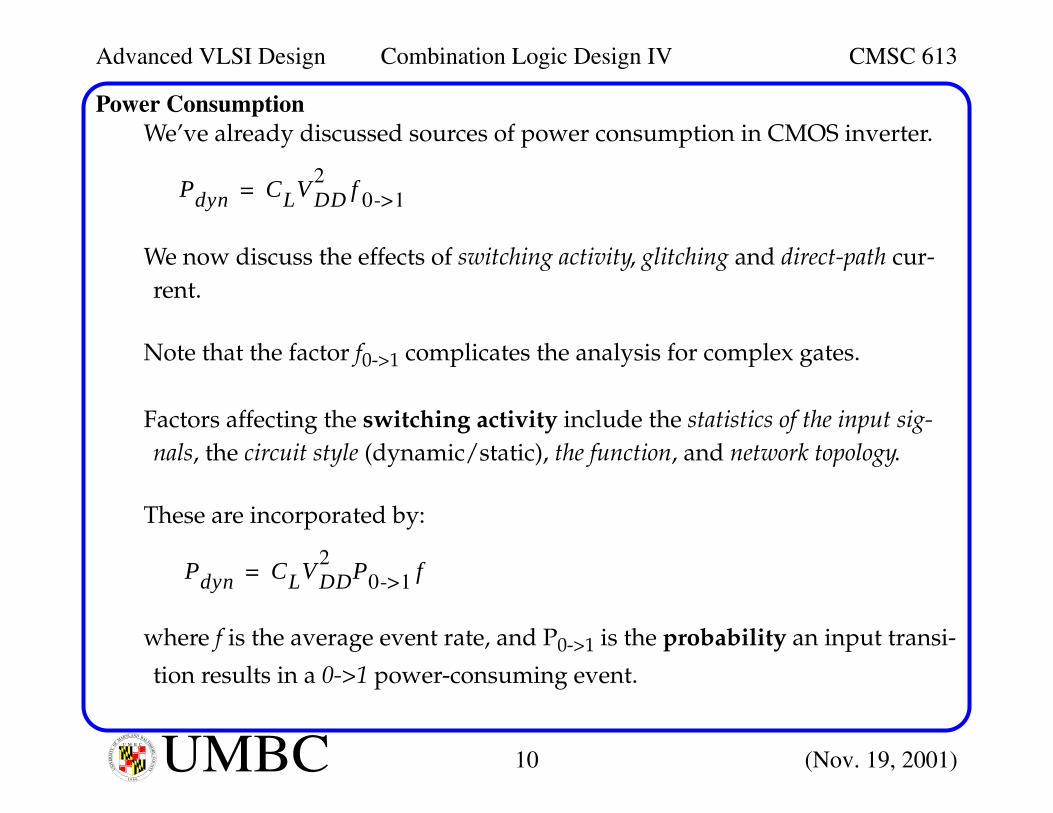
Power ConsumptionWe’ve already discussed sources of power consumption in CMOS inverter.
We now discuss the effects of switching activity, glitching and direct-path cur-rent.
Note that the factor f0->1 complicates the analysis for complex gates.
Factors affecting the switching activity include the statistics of the input sig-nals, the circuit style (dynamic/static), the function, and network topology.
These are incorporated by:
where f is the average event rate, and P0->1 is the probability an input transi-
tion results in a 0->1 power-consuming event.
Pdyn CLV DD2
f 0->1=
Pdyn CLV DD2
P0->1 f=
Advanced VLSI Design Combination Logic Design IV CMSC 613
11 (Nov. 19, 2001)UMBCU M B C
UN
IVE
RSI
TY
OF
MARYLAND BALTIM
OR
E C
OU
NTY
1 9 6 6
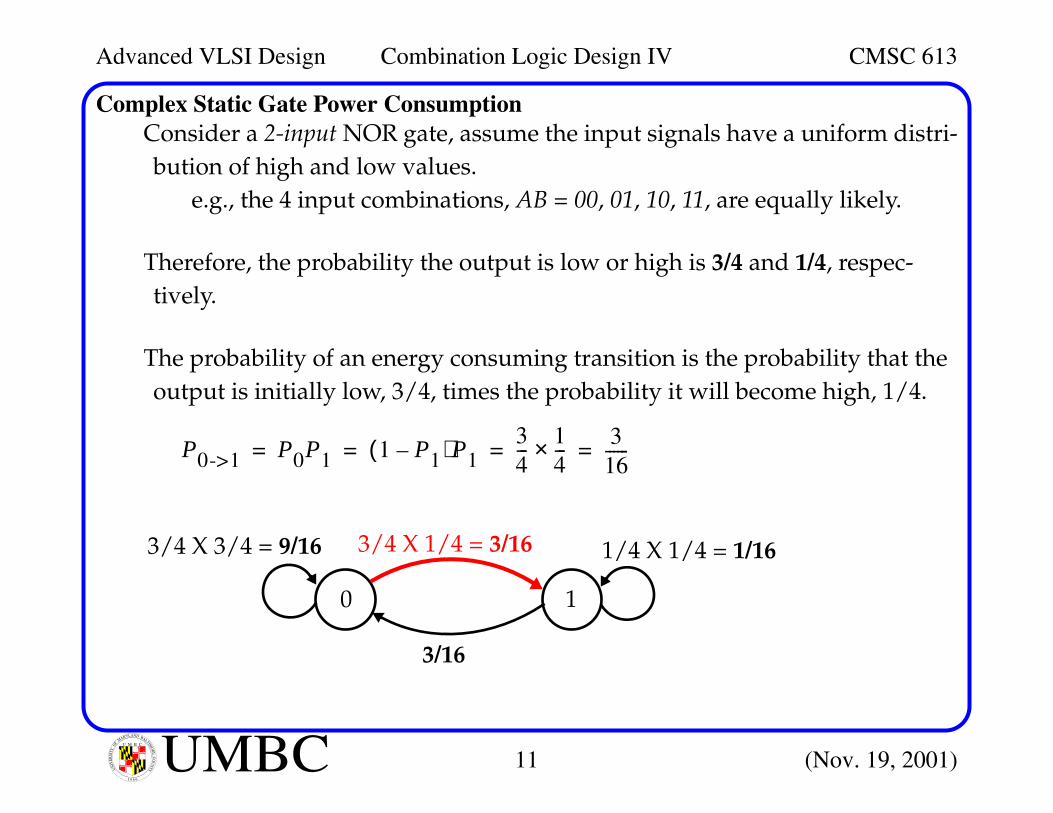
Complex Static Gate Power ConsumptionConsider a 2-input NOR gate, assume the input signals have a uniform distri-bution of high and low values.
e.g., the 4 input combinations, AB = 00, 01, 10, 11, are equally likely.
Therefore, the probability the output is low or high is 3/4 and 1/4, respec-tively.
The probability of an energy consuming transition is the probability that theoutput is initially low, 3/4, times the probability it will become high, 1/4.
P0->1 P0P1 1 P1–( )P134--- 1
4---× 3
16------= = = =
3/4 X 1/4 = 3/16
3/16
1/4 X 1/4 = 1/163/4 X 3/4 = 9/16
0 1
Advanced VLSI Design Combination Logic Design IV CMSC 613
12 (Nov. 19, 2001)UMBCU M B C
UN
IVE
RSI
TY
OF
MARYLAND BALTIM
OR
E C
OU
NTY
1 9 6 6
Complex Static Gate Power ConsumptionNote that the output probabilities are no longer uniform.
This suggests that the input signals are not uniform, since gates are typicallycascaded.
The probability that the output is 1 (P1) is a function of the input distributions,
PA and PB (the probabilities the inputs are 1).
The transition probability is then:
3-D graph shown in text.
Derive these expressions for AND, OR and XOR.
P1 1 PA–( ) 1 PB–( )= for the NOR gate.
P0->1 1 P1–( )P1 1 1 PA–( ) 1 PB–( )–[ ] 1 PA–( ) 1 PB–( )[ ]= =
Advanced VLSI Design Combination Logic Design IV CMSC 613
13 (Nov. 19, 2001)UMBCU M B C
UN
IVE
RSI
TY
OF
MARYLAND BALTIM
OR
E C
OU
NTY
1 9 6 6
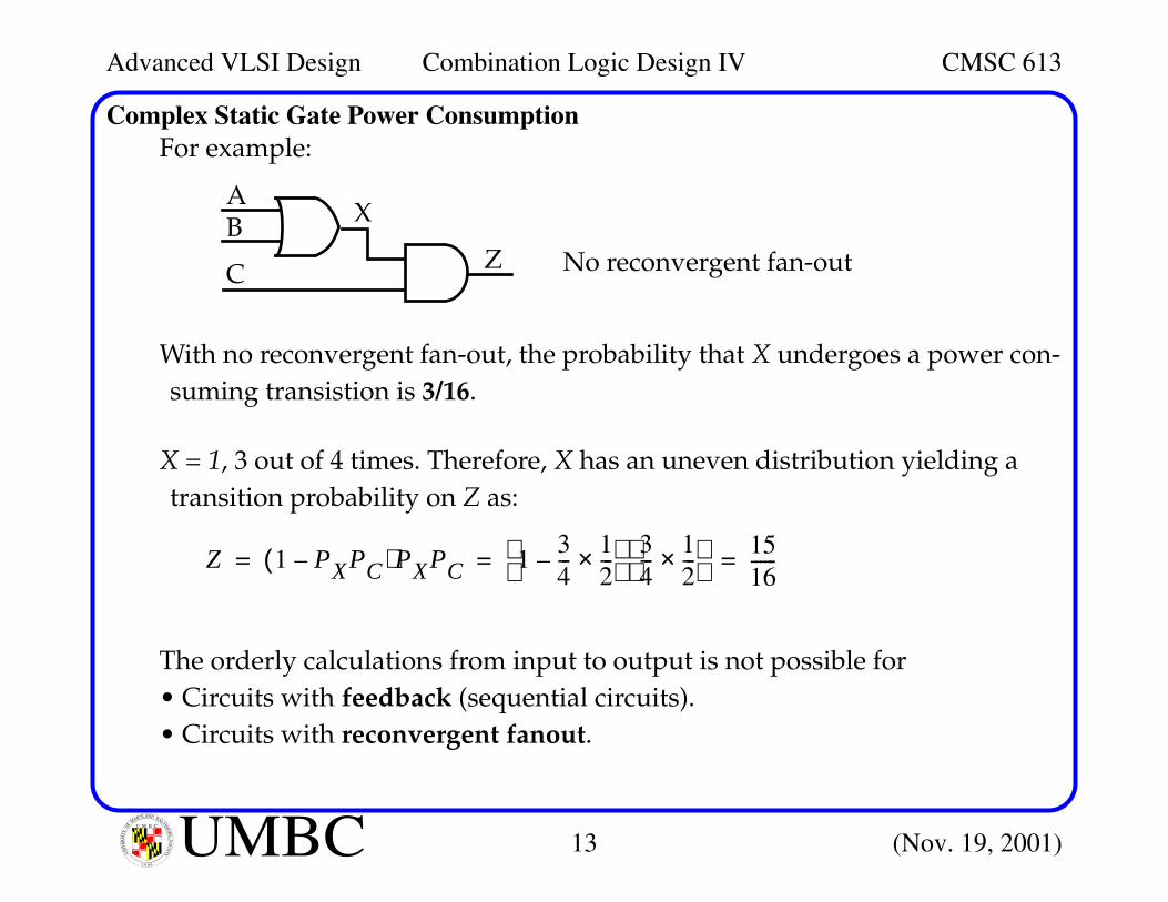
Complex Static Gate Power ConsumptionFor example:
With no reconvergent fan-out, the probability that X undergoes a power con-suming transistion is 3/16.
X = 1, 3 out of 4 times. Therefore, X has an uneven distribution yielding atransition probability on Z as:
The orderly calculations from input to output is not possible for• Circuits with feedback (sequential circuits).• Circuits with reconvergent fanout.
XAB
C Z No reconvergent fan-out
Z 1 PXPC–( )PXPC 134--- 1
2---×–
34--- 1
2---×
1516------= = =
Advanced VLSI Design Combination Logic Design IV CMSC 613
14 (Nov. 19, 2001)UMBCU M B C
UN
IVE
RSI
TY
OF
MARYLAND BALTIM
OR
E C
OU
NTY
1 9 6 6
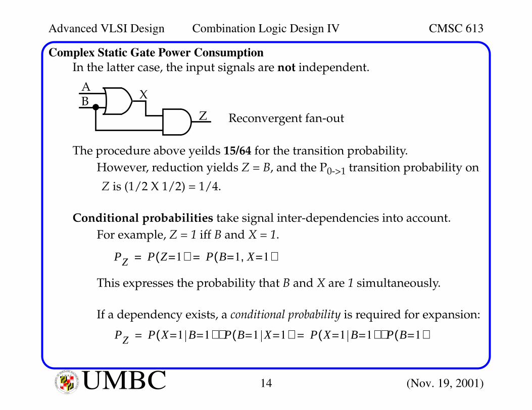
Complex Static Gate Power ConsumptionIn the latter case, the input signals are not independent.
The procedure above yeilds 15/64 for the transition probability.However, reduction yields Z = B, and the P0->1 transition probability on
Z is (1/2 X 1/2) = 1/4.
Conditional probabilities take signal inter-dependencies into account.For example, Z = 1 iff B and X = 1.
This expresses the probability that B and X are 1 simultaneously.
If a dependency exists, a conditional probability is required for expansion:
X
Z Reconvergent fan-out
AB
PZ P Z=1( ) P B=1 X=1,( )= =
PZ P X=1 B=1( ) P B=1 X=1( )⋅ P X=1 B=1( ) P B=1( )⋅= =
Advanced VLSI Design Combination Logic Design IV CMSC 613
15 (Nov. 19, 2001)UMBCU M B C
UN
IVE
RSI
TY
OF
MARYLAND BALTIM
OR
E C
OU
NTY
1 9 6 6
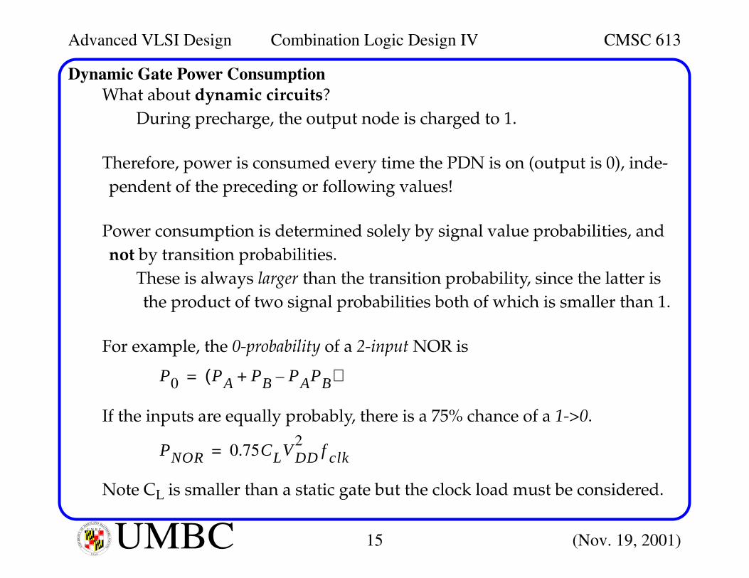
Dynamic Gate Power ConsumptionWhat about dynamic circuits?
During precharge, the output node is charged to 1.
Therefore, power is consumed every time the PDN is on (output is 0), inde-pendent of the preceding or following values!
Power consumption is determined solely by signal value probabilities, andnot by transition probabilities.
These is always larger than the transition probability, since the latter isthe product of two signal probabilities both of which is smaller than 1.
For example, the 0-probability of a 2-input NOR is
If the inputs are equally probably, there is a 75% chance of a 1->0.
Note CL is smaller than a static gate but the clock load must be considered.
P0 PA PB PAPB–+( )=
PNOR 0.75CLV DD2
f clk=
Advanced VLSI Design Combination Logic Design IV CMSC 613
16 (Nov. 19, 2001)UMBCU M B C
UN
IVE
RSI
TY
OF
MARYLAND BALTIM
OR
E C
OU
NTY
1 9 6 6
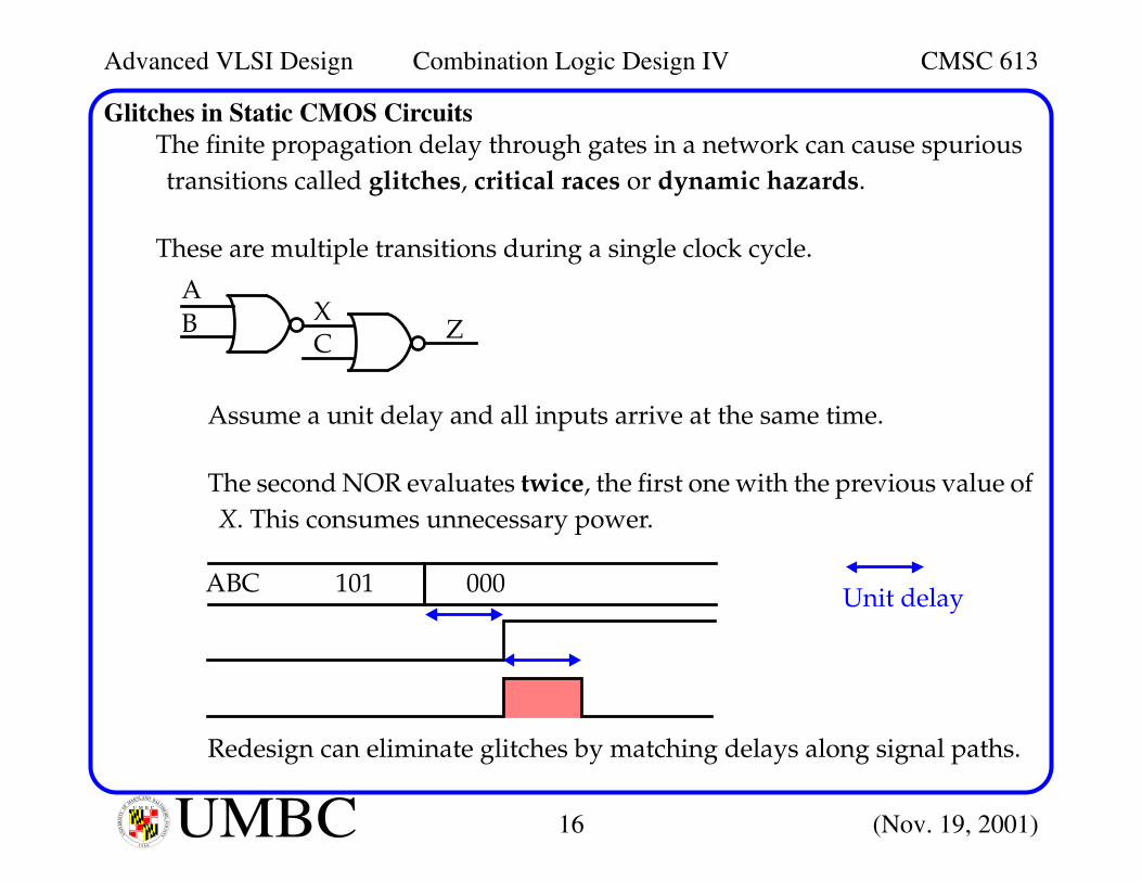
Glitches in Static CMOS CircuitsThe finite propagation delay through gates in a network can cause spurioustransitions called glitches, critical races or dynamic hazards.
These are multiple transitions during a single clock cycle.
Assume a unit delay and all inputs arrive at the same time.
The second NOR evaluates twice, the first one with the previous value ofX. This consumes unnecessary power.
Redesign can eliminate glitches by matching delays along signal paths.
AB
CX
Z
ABC 101 000 Unit delay
Advanced VLSI Design Combination Logic Design IV CMSC 613
17 (Nov. 19, 2001)UMBCU M B C
UN
IVE
RSI
TY
OF
MARYLAND BALTIM
OR
E C
OU
NTY
1 9 6 6
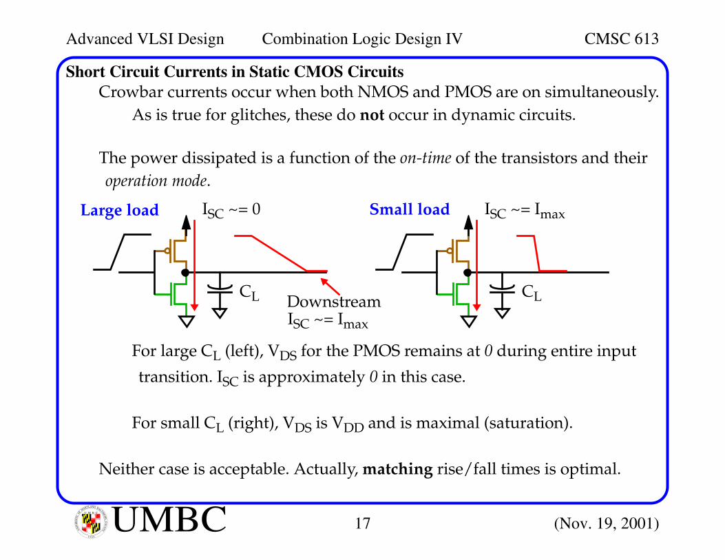
Short Circuit Currents in Static CMOS CircuitsCrowbar currents occur when both NMOS and PMOS are on simultaneously.
As is true for glitches, these do not occur in dynamic circuits.
The power dissipated is a function of the on-time of the transistors and theiroperation mode.
For large CL (left), VDS for the PMOS remains at 0 during entire input
transition. ISC is approximately 0 in this case.
For small CL (right), VDS is VDD and is maximal (saturation).
Neither case is acceptable. Actually, matching rise/fall times is optimal.
CL
ISC ~= 0
CL
ISC ~= Imax
DownstreamISC ~= Imax
Large load Small load
Advanced VLSI Design Combination Logic Design IV CMSC 613
18 (Nov. 19, 2001)UMBCU M B C
UN
IVE
RSI
TY
OF
MARYLAND BALTIM
OR
E C
OU
NTY
1 9 6 6
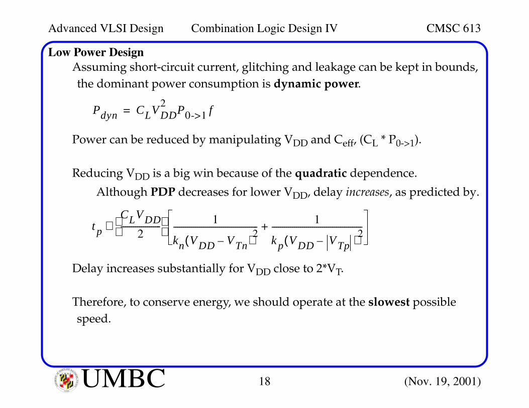
Low Power DesignAssuming short-circuit current, glitching and leakage can be kept in bounds,the dominant power consumption is dynamic power.
Power can be reduced by manipulating VDD and Ceff, (CL * P0->1).
Reducing VDD is a big win because of the quadratic dependence.
Although PDP decreases for lower VDD, delay increases, as predicted by.
Delay increases substantially for VDD close to 2*VT.
Therefore, to conserve energy, we should operate at the slowest possiblespeed.
Pdyn CLV DD2
P0->1 f=
t p
CLV DD2
-------------------- 1
kn V DD VTn–( )2------------------------------------------ 1
k p V DD VTp–( )2---------------------------------------------+∼
Advanced VLSI Design Combination Logic Design IV CMSC 613
19 (Nov. 19, 2001)UMBCU M B C
UN
IVE
RSI
TY
OF
MARYLAND BALTIM
OR
E C
OU
NTY
1 9 6 6
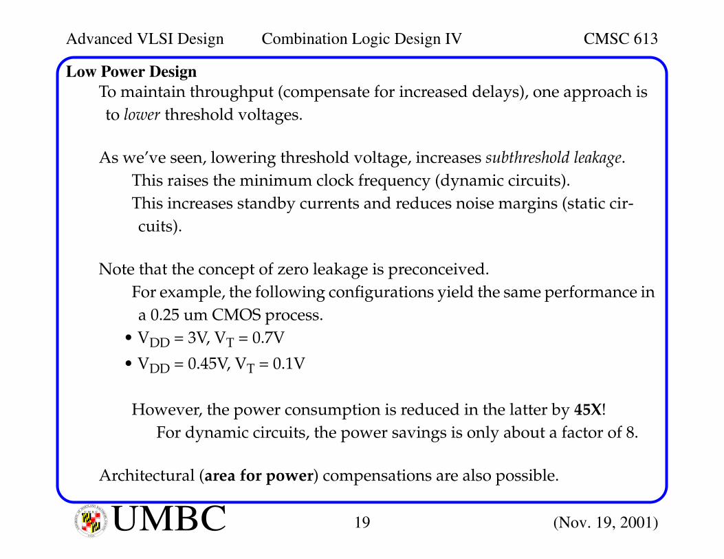
Low Power DesignTo maintain throughput (compensate for increased delays), one approach isto lower threshold voltages.
As we’ve seen, lowering threshold voltage, increases subthreshold leakage.This raises the minimum clock frequency (dynamic circuits).This increases standby currents and reduces noise margins (static cir-cuits).
Note that the concept of zero leakage is preconceived.For example, the following configurations yield the same performance ina 0.25 um CMOS process.
• VDD = 3V, VT = 0.7V
• VDD = 0.45V, VT = 0.1V
However, the power consumption is reduced in the latter by 45X!For dynamic circuits, the power savings is only about a factor of 8.
Architectural (area for power) compensations are also possible.

Advanced VLSI Design Combination Logic Design IV CMSC 613
20 (Nov. 19, 2001)UMBCU M B C
UN
IVE
RSI
TY
OF
MARYLAND BALTIM
OR
E C
OU
NTY
1 9 6 6
Low Power DesignWhen power supply voltage is lower bound due of external constraints orperformance, the only other means is to reduce Ceff.
This is achieved by reducing both the physical cap. and switching activity.
Lowering the physical cap. usually improves performance as well.For example, a CPL adder reportedly uses 30% less power (at 4V) com-pared with a static version.
Since most cap. is due to transistor cap. (diffusion and gate), this suggests theuse of minimum sized devices whenever possible.
Larger is only justified for large fan-outs and wiring capacitances.
Note this contradicts the standard cell philosophy which use larger tran-sistors in order to accommodate a wider ranges of loads.
Reducing switching activity can be accomplished by point-to-point buses andre-ordering inputs to gates (see text for examples).
Advanced VLSI Design Combination Logic Design IV CMSC 613
21 (Nov. 19, 2001)UMBCU M B C
UN
IVE
RSI
TY
OF
MARYLAND BALTIM
OR
E C
OU
NTY
1 9 6 6
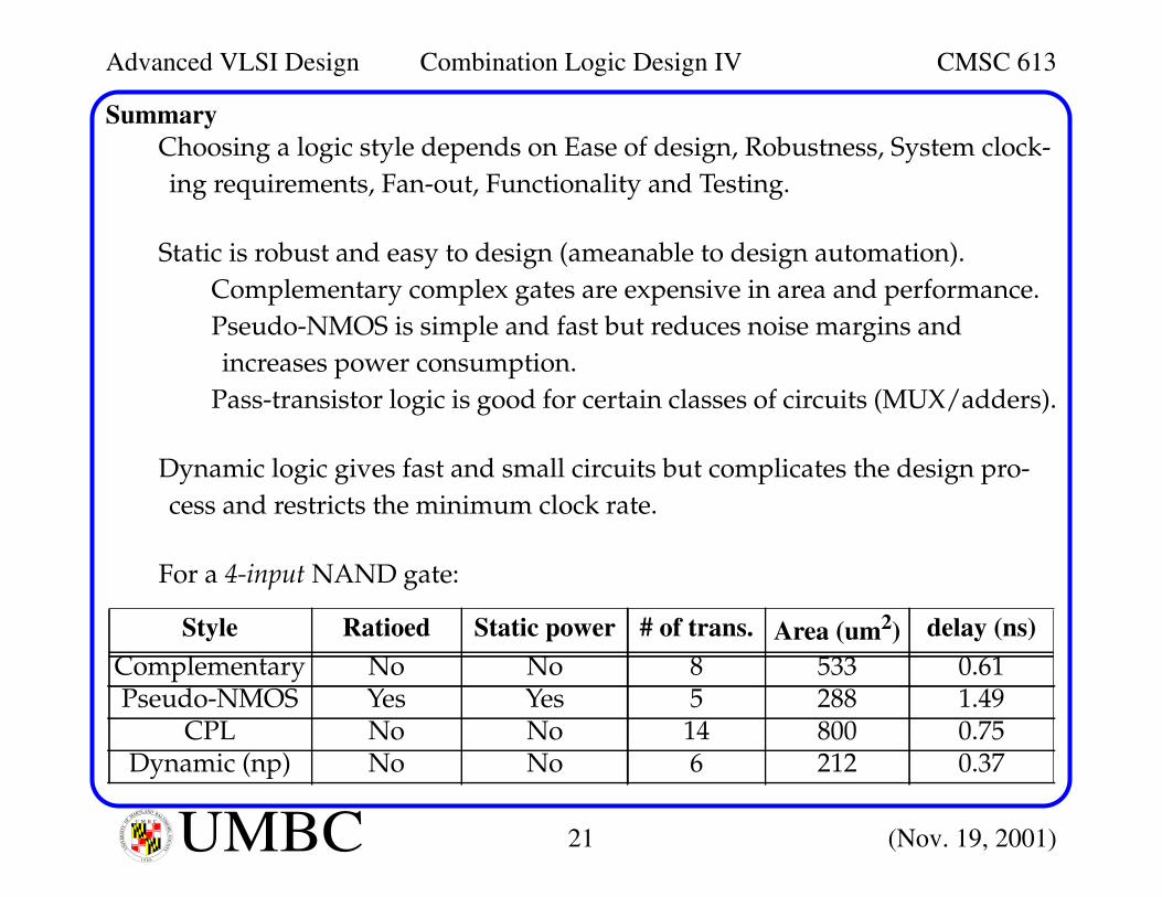
SummaryChoosing a logic style depends on Ease of design, Robustness, System clock-ing requirements, Fan-out, Functionality and Testing.
Static is robust and easy to design (ameanable to design automation).Complementary complex gates are expensive in area and performance.Pseudo-NMOS is simple and fast but reduces noise margins andincreases power consumption.
Pass-transistor logic is good for certain classes of circuits (MUX/adders).
Dynamic logic gives fast and small circuits but complicates the design pro-cess and restricts the minimum clock rate.
For a 4-input NAND gate:
Style Ratioed Static power # of trans. Area (um2) delay (ns)
Complementary No No 8 533 0.61Pseudo-NMOS Yes Yes 5 288 1.49
CPL No No 14 800 0.75Dynamic (np) No No 6 212 0.37
![arXiv:1409.6352v2 [math.NT] 22 Nov 2014](https://static.fdocument.org/doc/165x107/61f1fadb9b3b4b392434ee9b/arxiv14096352v2-mathnt-22-nov-2014.jpg)
![arXiv:2111.04391v1 [math.OC] 8 Nov 2021](https://static.fdocument.org/doc/165x107/61d35e3d10581779f3727cb5/arxiv211104391v1-mathoc-8-nov-2021.jpg)

![Abstract arXiv:1511.00361v1 [nucl-ex] 2 Nov 2015](https://static.fdocument.org/doc/165x107/628161d1545d83329c32cb69/abstract-arxiv151100361v1-nucl-ex-2-nov-2015.jpg)


![arXiv:2011.07066v1 [astro-ph.HE] 13 Nov 2020](https://static.fdocument.org/doc/165x107/6235792f1ae58523e26d2367/arxiv201107066v1-astro-phhe-13-nov-2020.jpg)


![arXiv:2011.08773v1 [math.NT] 17 Nov 2020](https://static.fdocument.org/doc/165x107/616893ffd394e9041f70c819/arxiv201108773v1-mathnt-17-nov-2020.jpg)

![arXiv:2110.15436v5 [math.DG] 15 Nov 2021](https://static.fdocument.org/doc/165x107/625351cd4a84c9358666c109/arxiv211015436v5-mathdg-15-nov-2021.jpg)
![arXiv:0911.2337v1 [cond-mat.mes-hall] 12 Nov 2009](https://static.fdocument.org/doc/165x107/620a9f233d6b396922728a08/arxiv09112337v1-cond-matmes-hall-12-nov-2009.jpg)
![arXiv:2012.00156v1 [astro-ph.HE] 30 Nov 2020](https://static.fdocument.org/doc/165x107/629625e8c97559211d768d53/arxiv201200156v1-astro-phhe-30-nov-2020.jpg)
![arXiv:2111.07374v1 [math.AP] 14 Nov 2021](https://static.fdocument.org/doc/165x107/6266f94462730772776e7a6b/arxiv211107374v1-mathap-14-nov-2021.jpg)
![arXiv:1408.3858v3 [math.CO] 30 Nov 2015](https://static.fdocument.org/doc/165x107/61aad0fff556580fb75f94c4/arxiv14083858v3-mathco-30-nov-2015.jpg)