TS5A23157 Dual 10-ΩSPDT Analog Switch - TI.com · TS5A23157 SCDS165E–MAY 2004–REVISED JUNE...
30
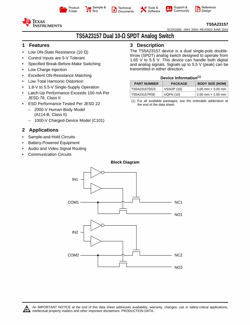
NC1 COM1 IN1 NO1 NC2 COM2 IN2 NO2 Product Folder Sample & Buy Technical Documents Tools & Software Support & Community Reference Design TS5A23157 SCDS165E – MAY 2004 – REVISED JUNE 2015 TS5A23157 Dual 10-Ω SPDT Analog Switch 1 Features 3 Description The TS5A23157 device is a dual single-pole double- 1• Low ON-State Resistance (10 Ω) throw (SPDT) analog switch designed to operate from • Control Inputs are 5-V Tolerant 1.65 V to 5.5 V. This device can handle both digital • Specified Break-Before-Make Switching and analog signals. Signals up to 5.5 V (peak) can be transmitted in either direction. • Low Charge Injection • Excellent ON-Resistance Matching Device Information (1) • Low Total Harmonic Distortion PART NUMBER PACKAGE BODY SIZE (NOM) • 1.8-V to 5.5-V Single-Supply Operation TS5A23157DGS VSSOP (10) 3.00 mm × 3.00 mm • Latch-Up Performance Exceeds 100 mA Per TS5A23157RSE UQFN (10) 2.00 mm × 1.50 mm JESD 78, Class II (1) For all available packages, see the orderable addendum at • ESD Performance Tested Per JESD 22 the end of the data sheet. – 2000-V Human-Body Model (A114-B, Class II) – 1000-V Charged-Device Model (C101) 2 Applications • Sample-and-Hold Circuits • Battery-Powered Equipment • Audio and Video Signal Routing • Communication Circuits Block Diagram 1 An IMPORTANT NOTICE at the end of this data sheet addresses availability, warranty, changes, use in safety-critical applications, intellectual property matters and other important disclaimers. PRODUCTION DATA.
Transcript of TS5A23157 Dual 10-ΩSPDT Analog Switch - TI.com · TS5A23157 SCDS165E–MAY 2004–REVISED JUNE...
NC1COM1
IN1
NO1
NC2COM2
IN2
NO2
Product
Folder
Sample &Buy
Technical
Documents
Tools &
Software
Support &Community
ReferenceDesign
TS5A23157SCDS165E –MAY 2004–REVISED JUNE 2015
TS5A23157 Dual 10-Ω SPDT Analog Switch1 Features 3 Description
The TS5A23157 device is a dual single-pole double-1• Low ON-State Resistance (10 Ω)
throw (SPDT) analog switch designed to operate from• Control Inputs are 5-V Tolerant 1.65 V to 5.5 V. This device can handle both digital• Specified Break-Before-Make Switching and analog signals. Signals up to 5.5 V (peak) can be
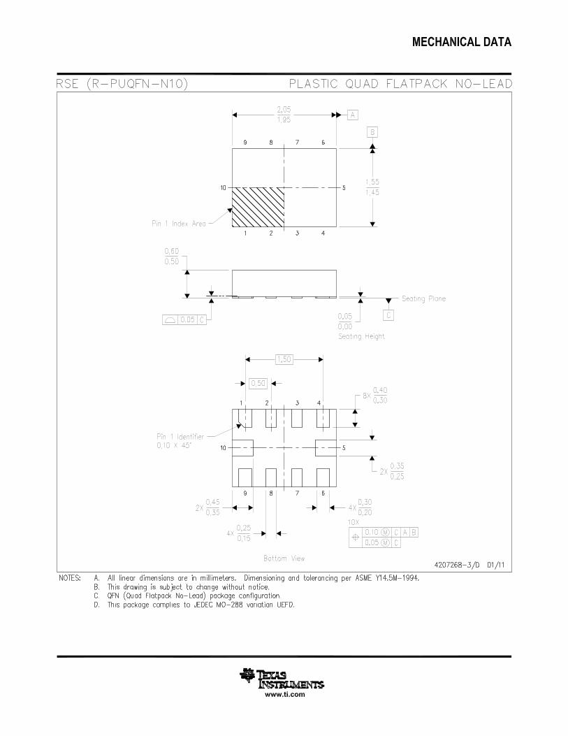
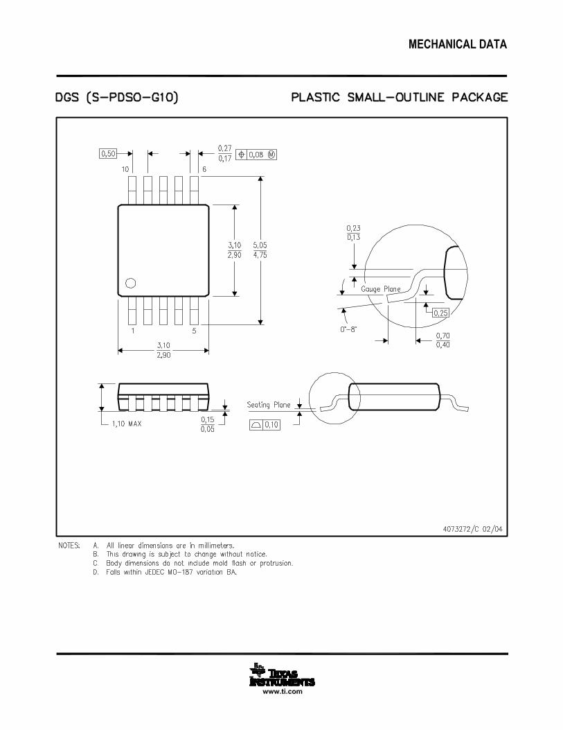
transmitted in either direction.• Low Charge Injection• Excellent ON-Resistance Matching Device Information(1)• Low Total Harmonic Distortion PART NUMBER PACKAGE BODY SIZE (NOM)• 1.8-V to 5.5-V Single-Supply Operation TS5A23157DGS VSSOP (10) 3.00 mm × 3.00 mm• Latch-Up Performance Exceeds 100 mA Per TS5A23157RSE UQFN (10) 2.00 mm × 1.50 mm
JESD 78, Class II(1) For all available packages, see the orderable addendum at
• ESD Performance Tested Per JESD 22 the end of the data sheet.– 2000-V Human-Body Model
(A114-B, Class II)– 1000-V Charged-Device Model (C101)
2 Applications• Sample-and-Hold Circuits• Battery-Powered Equipment• Audio and Video Signal Routing• Communication Circuits
Block Diagram
1
An IMPORTANT NOTICE at the end of this data sheet addresses availability, warranty, changes, use in safety-critical applications,intellectual property matters and other important disclaimers. PRODUCTION DATA.
TS5A23157SCDS165E –MAY 2004–REVISED JUNE 2015 www.ti.com
Table of Contents8.2 Functional Block Diagram ....................................... 161 Features .................................................................. 18.3 Feature Description................................................. 162 Applications ........................................................... 18.4 Device Functional Modes........................................ 163 Description ............................................................. 1
9 Application and Implementation ........................ 174 Revision History..................................................... 29.1 Application Information............................................ 175 Pin Configuration and Functions ......................... 39.2 Typical Application ................................................. 176 Specifications......................................................... 4
10 Power Supply Recommendations ..................... 186.1 Absolute Maximum Ratings ...................................... 411 Layout................................................................... 186.2 ESD Ratings.............................................................. 4
11.1 Layout Guidelines ................................................. 186.3 Recommended Operating Conditions....................... 411.2 Layout Example .................................................... 196.4 Thermal Information .................................................. 4
12 Device and Documentation Support ................. 196.5 Electrical Characteristics for 5-V Supply................... 512.1 Device Support .................................................... 196.6 Electrical Characteristics for 3.3-V Supply................ 612.2 Documentation Support ....................................... 216.7 Electrical Characteristics for 2.5-V Supply................ 712.3 Community Resources.......................................... 216.8 Electrical Characteristics for 1.8-V Supply................ 812.4 Trademarks ........................................................... 216.9 Typical Characteristics ............................................ 1012.5 Electrostatic Discharge Caution............................ 217 Parameter Measurement Information ................ 1212.6 Glossary ................................................................ 218 Detailed Description ............................................ 16
13 Mechanical, Packaging, and Orderable8.1 Overview ................................................................. 16Information ........................................................... 21
4 Revision HistoryNOTE: Page numbers for previous revisions may differ from page numbers in the current version.
Changes from Revision D (October 2013) to Revision E Page
• Added Pin Configuration and Functions section, ESD Ratings table, Feature Description section, Device FunctionalModes, Application and Implementation section, Power Supply Recommendations section, Layout section, Deviceand Documentation Support section, and Mechanical, Packaging, and Orderable Information section .............................. 1
2 Submit Documentation Feedback Copyright © 2004–2015, Texas Instruments Incorporated
Product Folder Links: TS5A23157
NC1
V+
NC2
COM2
IN1
NO1
GND
NO2
COM1
IN2
1
2
3
4 5 6
7
8
910
IN2
1
2
3
4
5
10
9
8
7
6
IN1
NO1
GND
NO2
V+
NC1
COM1
NC2
COM2
TS5A23157www.ti.com SCDS165E –MAY 2004–REVISED JUNE 2015
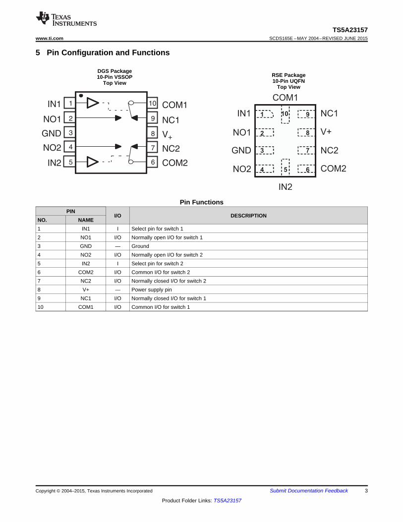
5 Pin Configuration and Functions
DGS PackageRSE Package10-Pin VSSOP10-Pin UQFNTop View
Top View
Pin FunctionsPIN
I/O DESCRIPTIONNO. NAME1 IN1 I Select pin for switch 12 NO1 I/O Normally open I/O for switch 13 GND — Ground4 NO2 I/O Normally open I/O for switch 25 IN2 I Select pin for switch 26 COM2 I/O Common I/O for switch 27 NC2 I/O Normally closed I/O for switch 28 V+ — Power supply pin9 NC1 I/O Normally closed I/O for switch 110 COM1 I/O Common I/O for switch 1
Copyright © 2004–2015, Texas Instruments Incorporated Submit Documentation Feedback 3
Product Folder Links: TS5A23157
TS5A23157SCDS165E –MAY 2004–REVISED JUNE 2015 www.ti.com
6 Specifications
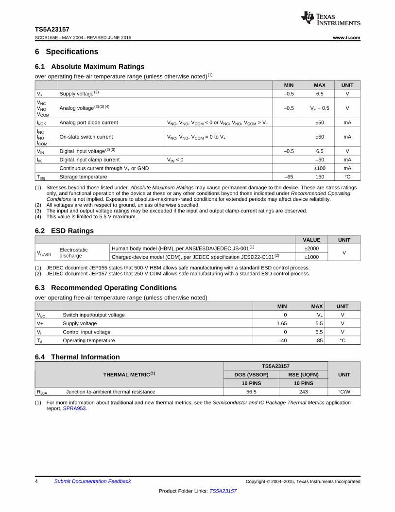
6.1 Absolute Maximum Ratingsover operating free-air temperature range (unless otherwise noted) (1)
MIN MAX UNITV+ Supply voltage (2) –0.5 6.5 VVNCVNO Analog voltage (2) (3) (4) –0.5 V+ + 0.5 VVCOM
II/OK Analog port diode current VNC, VNO, VCOM < 0 or VNC, VNO, VCOM > V+ ±50 mAINCINO On-state switch current VNC, VNO, VCOM = 0 to V+ ±50 mAICOM
VIN Digital input voltage (2) (3) –0.5 6.5 VIIK Digital input clamp current VIN < 0 –50 mA
Continuous current through V+ or GND ±100 mATstg Storage temperature –65 150 °C
(1) Stresses beyond those listed under Absolute Maximum Ratings may cause permanent damage to the device. These are stress ratingsonly, and functional operation of the device at these or any other conditions beyond those indicated under Recommended OperatingConditions is not implied. Exposure to absolute-maximum-rated conditions for extended periods may affect device reliability.
(2) All voltages are with respect to ground, unless otherwise specified.(3) The input and output voltage ratings may be exceeded if the input and output clamp-current ratings are observed.(4) This value is limited to 5.5 V maximum.
6.2 ESD RatingsVALUE UNIT
Human body model (HBM), per ANSI/ESDA/JEDEC JS-001 (1) ±2000ElectrostaticV(ESD) Vdischarge Charged-device model (CDM), per JEDEC specification JESD22-C101 (2) ±1000
(1) JEDEC document JEP155 states that 500-V HBM allows safe manufacturing with a standard ESD control process.(2) JEDEC document JEP157 states that 250-V CDM allows safe manufacturing with a standard ESD control process.
6.3 Recommended Operating Conditionsover operating free-air temperature range (unless otherwise noted)
MIN MAX UNITVI/O Switch input/output voltage 0 V+ VV+ Supply voltage 1.65 5.5 VVI Control input voltage 0 5.5 VTA Operating temperature –40 85 °C
6.4 Thermal InformationTS5A23157
THERMAL METRIC (1) DGS (VSSOP) RSE (UQFN) UNIT10 PINS 10 PINS
RθJA Junction-to-ambient thermal resistance 56.5 243 °C/W
(1) For more information about traditional and new thermal metrics, see the Semiconductor and IC Package Thermal Metrics applicationreport, SPRA953.
4 Submit Documentation Feedback Copyright © 2004–2015, Texas Instruments Incorporated
Product Folder Links: TS5A23157
TS5A23157www.ti.com SCDS165E –MAY 2004–REVISED JUNE 2015
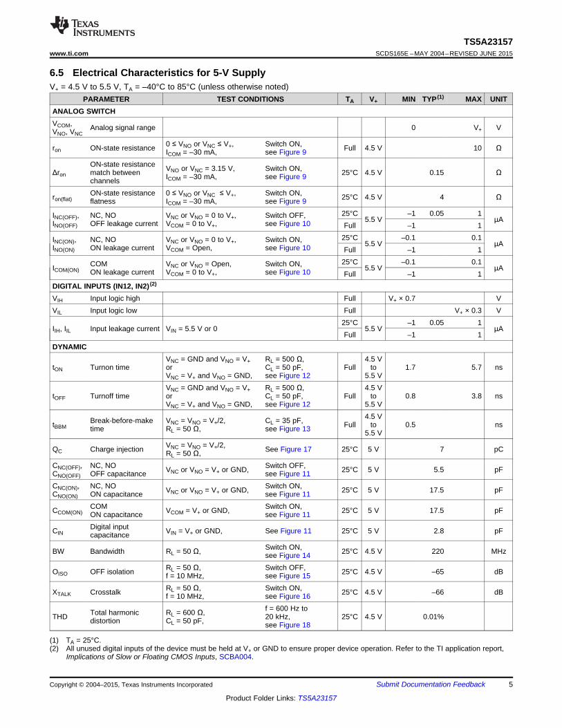
6.5 Electrical Characteristics for 5-V SupplyV+ = 4.5 V to 5.5 V, TA = –40°C to 85°C (unless otherwise noted)
PARAMETER TEST CONDITIONS TA V+ MIN TYP (1) MAX UNITANALOG SWITCHVCOM, Analog signal range 0 V+ VVNO, VNC
0 ≤ VNO or VNC ≤ V+, Switch ON,ron ON-state resistance Full 4.5 V 10 ΩICOM = –30 mA, see Figure 9ON-state resistance VNO or VNC = 3.15 V, Switch ON,Δron match between 25°C 4.5 V 0.15 ΩICOM = –30 mA, see Figure 9channelsON-state resistance 0 ≤ VNO or VNC ≤ V+, Switch ON,ron(flat) 25°C 4.5 V 4 Ωflatness ICOM = –30 mA, see Figure 9
25°C –1 0.05 1INC(OFF), NC, NO VNC or VNO = 0 to V+, Switch OFF, 5.5 V µAINO(OFF) OFF leakage current VCOM = 0 to V+, see Figure 10 Full –1 125°C –0.1 0.1INC(ON), NC, NO VNC or VNO = 0 to V+, Switch ON, 5.5 V µAINO(ON) ON leakage current VCOM = Open, see Figure 10 Full –1 125°C –0.1 0.1COM VNC or VNO = Open, Switch ON,ICOM(ON) 5.5 V µAON leakage current VCOM = 0 to V+, see Figure 10 Full –1 1
DIGITAL INPUTS (IN12, IN2) (2)
VIH Input logic high Full V+ × 0.7 VVIL Input logic low Full V+ × 0.3 V
25°C –1 0.05 1IIH, IIL Input leakage current VIN = 5.5 V or 0 5.5 V µA
Full –1 1DYNAMIC
VNC = GND and VNO = V+ RL = 500 Ω, 4.5 VtON Turnon time or CL = 50 pF, Full to 1.7 5.7 ns
VNC = V+ and VNO = GND, see Figure 12 5.5 VVNC = GND and VNO = V+ RL = 500 Ω, 4.5 V
tOFF Turnoff time or CL = 50 pF, Full to 0.8 3.8 nsVNC = V+ and VNO = GND, see Figure 12 5.5 V
4.5 VBreak-before-make VNC = VNO = V+/2, CL = 35 pF,tBBM Full to 0.5 nstime RL = 50 Ω, see Figure 13 5.5 VVNC = VNO = V+/2,QC Charge injection See Figure 17 25°C 5 V 7 pCRL = 50 Ω,
CNC(OFF), NC, NO Switch OFF,VNC or VNO = V+ or GND, 25°C 5 V 5.5 pFCNO(OFF) OFF capacitance see Figure 11CNC(ON), NC, NO Switch ON,VNC or VNO = V+ or GND, 25°C 5 V 17.5 pFCNO(ON) ON capacitance see Figure 11
COM Switch ON,CCOM(ON) VCOM = V+ or GND, 25°C 5 V 17.5 pFON capacitance see Figure 11Digital inputCIN VIN = V+ or GND, See Figure 11 25°C 5 V 2.8 pFcapacitance
Switch ON,BW Bandwidth RL = 50 Ω, 25°C 4.5 V 220 MHzsee Figure 14RL = 50 Ω, Switch OFF,OISO OFF isolation 25°C 4.5 V –65 dBf = 10 MHz, see Figure 15RL = 50 Ω, Switch ON,XTALK Crosstalk 25°C 4.5 V –66 dBf = 10 MHz, see Figure 16
f = 600 Hz toTotal harmonic RL = 600 Ω,THD 20 kHz, 25°C 4.5 V 0.01%distortion CL = 50 pF, see Figure 18
(1) TA = 25°C.(2) All unused digital inputs of the device must be held at V+ or GND to ensure proper device operation. Refer to the TI application report,
Implications of Slow or Floating CMOS Inputs, SCBA004.
Copyright © 2004–2015, Texas Instruments Incorporated Submit Documentation Feedback 5
Product Folder Links: TS5A23157
TS5A23157SCDS165E –MAY 2004–REVISED JUNE 2015 www.ti.com
Electrical Characteristics for 5-V Supply (continued)V+ = 4.5 V to 5.5 V, TA = –40°C to 85°C (unless otherwise noted)
PARAMETER TEST CONDITIONS TA V+ MIN TYP (1) MAX UNITSUPPLY
25°C 1Positive supplyI+ VIN = V+ or GND, Switch ON or OFF 5.5 V µAcurrent Full 10Change inΔI+ VIN = V+ – 0.6 V Full 5.5 V 500 µAsupply current
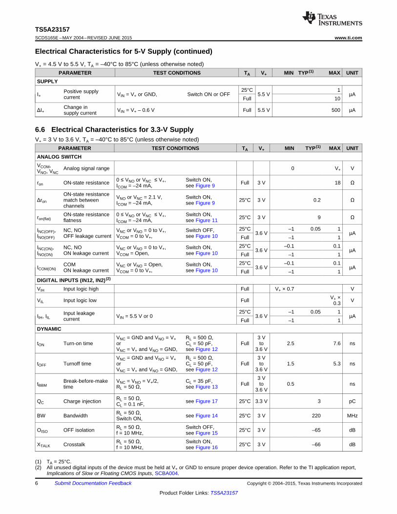
6.6 Electrical Characteristics for 3.3-V SupplyV+ = 3 V to 3.6 V, TA = –40°C to 85°C (unless otherwise noted)
PARAMETER TEST CONDITIONS TA V+ MIN TYP (1) MAX UNITANALOG SWITCHVCOM, Analog signal range 0 V+ VVNO, VNC
0 ≤ VNO or VNC ≤ V+, Switch ON,ron ON-state resistance Full 3 V 18 ΩICOM = –24 mA, see Figure 9ON-state resistance VNO or VNC = 2.1 V, Switch ON,Δron match between 25°C 3 V 0.2 ΩICOM = –24 mA, see Figure 9channelsON-state resistance 0 ≤ VNO or VNC ≤ V+, Switch ON,ron(flat) 25°C 3 V 9 Ωflatness ICOM = –24 mA, see Figure 11
25°C –1 0.05 1INC(OFF), NC, NO VNC or VNO = 0 to V+, Switch OFF, 3.6 V µAINO(OFF) OFF leakage current VCOM = 0 to V+, see Figure 10 Full –1 125°C –0.1 0.1INC(ON), NC, NO VNC or VNO = 0 to V+, Switch ON, 3.6 V µAINO(ON) ON leakage current VCOM = Open, see Figure 10 Full –1 125°C –0.1 0.1COM VNC or VNO = Open, Switch ON,ICOM(ON) 3.6 V µAON leakage current VCOM = 0 to V+, see Figure 10 Full –1 1
DIGITAL INPUTS (IN12, IN2) (2)
VIH Input logic high Full V+ × 0.7 VV+ ×VIL Input logic low Full V0.3
25°C –1 0.05 1Input leakageIIH, IIL VIN = 5.5 V or 0 3.6 V µAcurrent Full –1 1DYNAMIC
VNC = GND and VNO = V+ RL = 500 Ω, 3 VtON Turn-on time or CL = 50 pF, Full to 2.5 7.6 ns
VNC = V+ and VNO = GND, see Figure 12 3.6 VVNC = GND and VNO = V+ RL = 500 Ω, 3 V
tOFF Turnoff time or CL = 50 pF, Full to 1.5 5.3 nsVNC = V+ and VNO = GND, see Figure 12 3.6 V
3 VBreak-before-make VNC = VNO = V+/2, CL = 35 pF,tBBM Full to 0.5 nstime RL = 50 Ω, see Figure 13 3.6 VRL = 50 Ω,QC Charge injection see Figure 17 25°C 3.3 V 3 pCCL = 0.1 nF,RL = 50 Ω,BW Bandwidth see Figure 14 25°C 3 V 220 MHzSwitch ON,RL = 50 Ω, Switch OFF,OISO OFF isolation 25°C 3 V –65 dBf = 10 MHz, see Figure 15RL = 50 Ω, Switch ON,XTALK Crosstalk 25°C 3 V –66 dBf = 10 MHz, see Figure 16
(1) TA = 25°C.(2) All unused digital inputs of the device must be held at V+ or GND to ensure proper device operation. Refer to the TI application report,
Implications of Slow or Floating CMOS Inputs, SCBA004.
6 Submit Documentation Feedback Copyright © 2004–2015, Texas Instruments Incorporated
Product Folder Links: TS5A23157
TS5A23157www.ti.com SCDS165E –MAY 2004–REVISED JUNE 2015
Electrical Characteristics for 3.3-V Supply (continued)V+ = 3 V to 3.6 V, TA = –40°C to 85°C (unless otherwise noted)
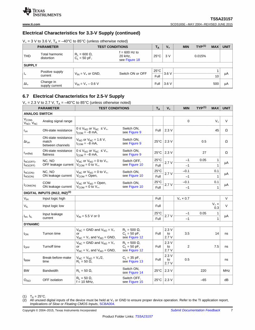
PARAMETER TEST CONDITIONS TA V+ MIN TYP (1) MAX UNITf = 600 Hz toTotal harmonic RL = 600 Ω,THD 20 kHz, 25°C 3 V 0.015%distortion CL = 50 pF, see Figure 18
SUPPLY25°C 1Positive supplyI+ VIN = V+ or GND, Switch ON or OFF 3.6 V µAcurrent Full 10
Change inΔI+ VIN = V+ – 0.6 V Full 3.6 V 500 µAsupply current
6.7 Electrical Characteristics for 2.5-V SupplyV+ = 2.3 V to 2.7 V, TA = –40°C to 85°C (unless otherwise noted)
PARAMETER TEST CONDITIONS TA V+ MIN TYP (1) MAX UNITANALOG SWITCHVCOM, Analog signal range 0 V+ VVNO, VNC
0 ≤ VNO or VNC ≤ V+, Switch ON,ron ON-state resistance Full 2.3 V 45 ΩICOM = –8 mA, see Figure 9ON-state resistance VNO or VNC = 1.6 V, Switch ON,Δron match 25°C 2.3 V 0.5 ΩICOM = –8 mA, see Figure 9between channelsON-state resistance 0 ≤ VNO or VNC ≤ V+, Switch ON,ron(flat) 25°C 2.3 V 27 Ωflatness ICOM = –8 mA, see Figure 9
25°C –1 0.05 1INC(OFF), NC, NO VNC or VNO = 0 to V+, Switch OFF, 2.7 V µAINO(OFF) OFF leakage current VCOM = 0 to V+, see Figure 10 Full –1 125°C –0.1 0.1INC(ON), NC, NO VNC or VNO = 0 to V+, Switch ON, 2.7 V µAINO(ON) ON leakage current VCOM = Open, see Figure 10 Full –1 125°C –0.1 0.1COM VNC or VNO = Open, Switch ON,ICOM(ON) 2.7 V µAON leakage current VCOM = 0 to V+, see Figure 10 Full –1 1
DIGITAL INPUTS (IN12, IN2) (2)
VIH Input logic high Full V+ × 0.7 VV+ ×VIL Input logic low Full V0.3
25°C –1 0.05 1Input leakageIIH, IIL VIN = 5.5 V or 0 2.7 V µAcurrent Full –1 1DYNAMIC
VNC = GND and VNO = V+ RL = 500 Ω, 2.3 VtON Turnon time or CL = 50 pF, Full to 3.5 14 ns
VNC = V+ and VNO = GND, see Figure 12 2.7 VVNC = GND and VNO = V+ RL = 500 Ω, 2.3 V
tOFF Turnoff time or CL = 50 pF, Full to 2 7.5 nsVNC = V+ and VNO = GND, see Figure 12 2.7 V
2.3 VBreak-before-make VNC = VNO = V+/2, CL = 35 pF,tBBM Full to 0.5 nstime RL = 50 Ω, see Figure 13 2.7 VSwitch ON,BW Bandwidth RL = 50 Ω, 25°C 2.3 V 220 MHzsee Figure 14
RL = 50 Ω, Switch OFF,OISO OFF isolation 25°C 2.3 V –65 dBf = 10 MHz, see Figure 15
(1) TA = 25°C.(2) All unused digital inputs of the device must be held at V+ or GND to ensure proper device operation. Refer to the TI application report,
Implications of Slow or Floating CMOS Inputs, SCBA004.
Copyright © 2004–2015, Texas Instruments Incorporated Submit Documentation Feedback 7
Product Folder Links: TS5A23157
TS5A23157SCDS165E –MAY 2004–REVISED JUNE 2015 www.ti.com
Electrical Characteristics for 2.5-V Supply (continued)V+ = 2.3 V to 2.7 V, TA = –40°C to 85°C (unless otherwise noted)
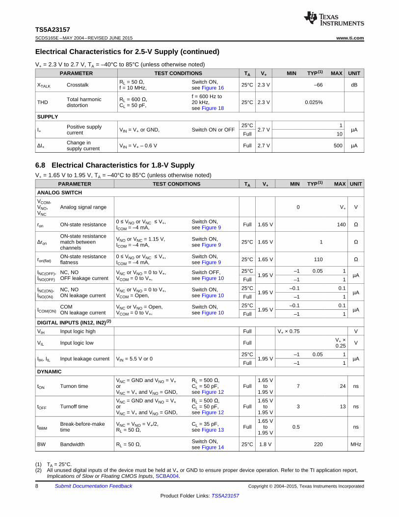
PARAMETER TEST CONDITIONS TA V+ MIN TYP (1) MAX UNITRL = 50 Ω, Switch ON,XTALK Crosstalk 25°C 2.3 V –66 dBf = 10 MHz, see Figure 16
f = 600 Hz toTotal harmonic RL = 600 Ω,THD 20 kHz, 25°C 2.3 V 0.025%distortion CL = 50 pF, see Figure 18SUPPLY
25°C 1Positive supplyI+ VIN = V+ or GND, Switch ON or OFF 2.7 V µAcurrent Full 10Change inΔI+ VIN = V+ – 0.6 V Full 2.7 V 500 µAsupply current
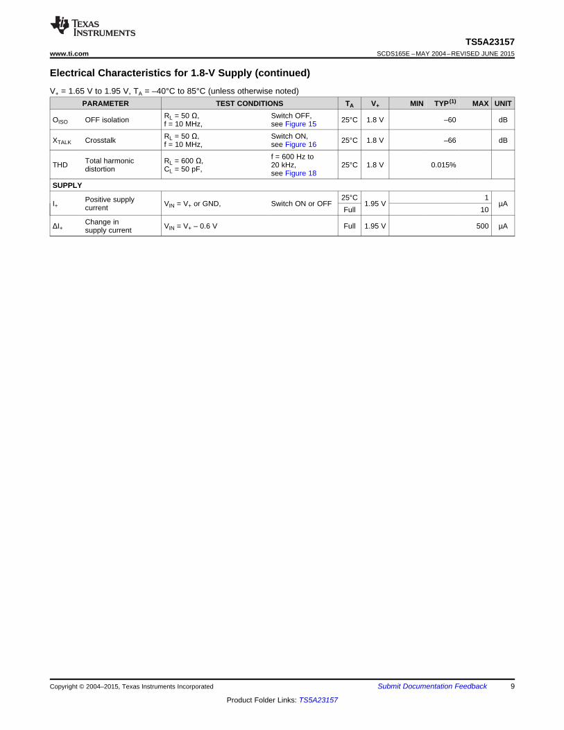
6.8 Electrical Characteristics for 1.8-V SupplyV+ = 1.65 V to 1.95 V, TA = –40°C to 85°C (unless otherwise noted)
PARAMETER TEST CONDITIONS TA V+ MIN TYP (1) MAX UNITANALOG SWITCHVCOM,VNO, Analog signal range 0 V+ VVNC
0 ≤ VNO or VNC ≤ V+, Switch ON,ron ON-state resistance Full 1.65 V 140 ΩICOM = –4 mA, see Figure 9ON-state resistance VNO or VNC = 1.15 V, Switch ON,Δron match between 25°C 1.65 V 1 ΩICOM = –4 mA, see Figure 9channelsON-state resistance 0 ≤ VNO or VNC ≤ V+, Switch ON,ron(flat) 25°C 1.65 V 110 Ωflatness ICOM = –4 mA, see Figure 9
25°C –1 0.05 1INC(OFF), NC, NO VNC or VNO = 0 to V+, Switch OFF, 1.95 V µAINO(OFF) OFF leakage current VCOM = 0 to V+, see Figure 10 Full –1 125°C –0.1 0.1INC(ON), NC, NO VNC or VNO = 0 to V+, Switch ON, 1.95 V µAINO(ON) ON leakage current VCOM = Open, see Figure 10 Full –1 125°C –0.1 0.1COM VNC or VNO = Open, Switch ON,ICOM(ON) 1.95 V µAON leakage current VCOM = 0 to V+, see Figure 10 Full –1 1
DIGITAL INPUTS (IN12, IN2) (2)
VIH Input logic high Full V+ × 0.75 VV+ ×VIL Input logic low Full V0.25
25°C –1 0.05 1IIH, IIL Input leakage current VIN = 5.5 V or 0 1.95 V µA
Full –1 1DYNAMIC
VNC = GND and VNO = V+ RL = 500 Ω, 1.65 VtON Turnon time or CL = 50 pF, Full to 7 24 ns
VNC = V+ and VNO = GND, see Figure 12 1.95 VVNC = GND and VNO = V+ RL = 500 Ω, 1.65 V
tOFF Turnoff time or CL = 50 pF, Full to 3 13 nsVNC = V+ and VNO = GND, see Figure 12 1.95 V
1.65 VBreak-before-make VNC = VNO = V+/2, CL = 35 pF,tBBM Full to 0.5 nstime RL = 50 Ω, see Figure 13 1.95 VSwitch ON,BW Bandwidth RL = 50 Ω, 25°C 1.8 V 220 MHzsee Figure 14
(1) TA = 25°C.(2) All unused digital inputs of the device must be held at V+ or GND to ensure proper device operation. Refer to the TI application report,
Implications of Slow or Floating CMOS Inputs, SCBA004.
8 Submit Documentation Feedback Copyright © 2004–2015, Texas Instruments Incorporated
Product Folder Links: TS5A23157
TS5A23157www.ti.com SCDS165E –MAY 2004–REVISED JUNE 2015
Electrical Characteristics for 1.8-V Supply (continued)V+ = 1.65 V to 1.95 V, TA = –40°C to 85°C (unless otherwise noted)
PARAMETER TEST CONDITIONS TA V+ MIN TYP (1) MAX UNITRL = 50 Ω, Switch OFF,OISO OFF isolation 25°C 1.8 V –60 dBf = 10 MHz, see Figure 15RL = 50 Ω, Switch ON,XTALK Crosstalk 25°C 1.8 V –66 dBf = 10 MHz, see Figure 16
f = 600 Hz toTotal harmonic RL = 600 Ω,THD 20 kHz, 25°C 1.8 V 0.015%distortion CL = 50 pF, see Figure 18SUPPLY
25°C 1Positive supplyI+ VIN = V+ or GND, Switch ON or OFF 1.95 V µAcurrent Full 10Change inΔI+ VIN = V+ – 0.6 V Full 1.95 V 500 µAsupply current
Copyright © 2004–2015, Texas Instruments Incorporated Submit Documentation Feedback 9
Product Folder Links: TS5A23157
0
1
2
3
4
5
−60 −40 −20 0 20 40 60 80 100
tON
tOFF
TA − Temperature − °C
t ON
/tO
FF
−n
s
tON
tOFF
0
2
4
6
8
10
12
1.5 2 2.5 3 3.5 4 4.5 5 5.5
V+ − Supply Voltage − V
t ON
/tO
FF
−n
s
TA = 25°C
4
6
8
10
0 1 2 3 4 5
VCOM − V
ro
n−
Ω
TA = +85°C
TA = +25°C
TA = −40°C
Temperature − °C
Leakag
e−
nA
−1
0
1
2
3
4
5
−60 −40 −20 0 20 40 60 80 100
INC(OFF), INO(OFF),
INC(ON), INO(ON), and
ICOM(ON)
OFF
ON
0
20
40
60
80
100
120
140
0 1 2 3 4 5
VCOM − V
V+ = 1.65 V
V+ = 2.3 V
V+ = 3 VV+ = 4.5 V
ro
n−
Ω
TA = 25°C
4
8
12
16
20
0 0.5 1 1.5 2 2.5 3 3.5
TA = +85 C°
TA = +25°C
TA = 40– °C
VCOM − V
ro
n−
Ω
TS5A23157SCDS165E –MAY 2004–REVISED JUNE 2015 www.ti.com
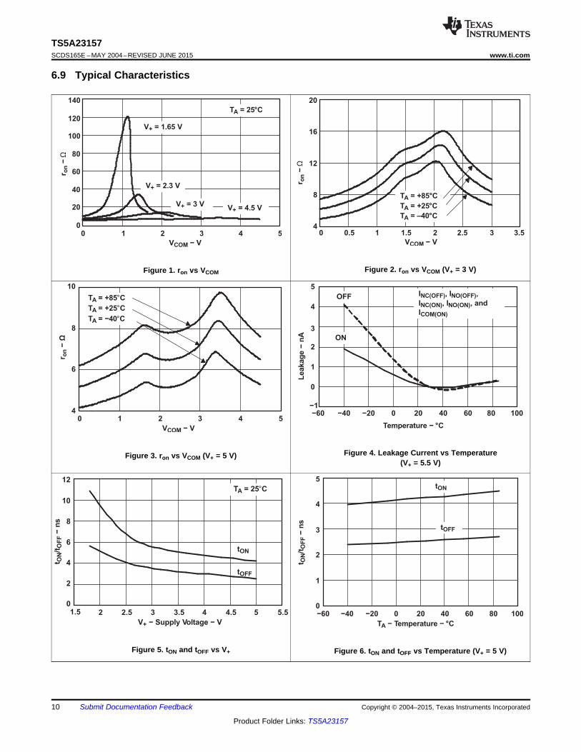
6.9 Typical Characteristics
Figure 2. ron vs VCOM (V+ = 3 V)Figure 1. ron vs VCOM
Figure 4. Leakage Current vs TemperatureFigure 3. ron vs VCOM (V+ = 5 V)(V+ = 5.5 V)
Figure 5. tON and tOFF vs V+ Figure 6. tON and tOFF vs Temperature (V+ = 5 V)
10 Submit Documentation Feedback Copyright © 2004–2015, Texas Instruments Incorporated
Product Folder Links: TS5A23157
−100
−90
−80
−70
−60
−50
−40
−30
−20
−10
0
10
0.1 1 10 100 1000Frequency − MHz
Lo
ss
−d
B
Bandwidth
Off-Isolation
Crosstalk
TA = 25°C
Frequency −Hz
TH
D +
No
ise
−%
0.0000
0.0002
0.0004
0.0006
0.0008
0.0010
0.0012
0.0014
0.0016
0.0018
0.0020
100 1000 10000
TA = 25°C
TS5A23157www.ti.com SCDS165E –MAY 2004–REVISED JUNE 2015
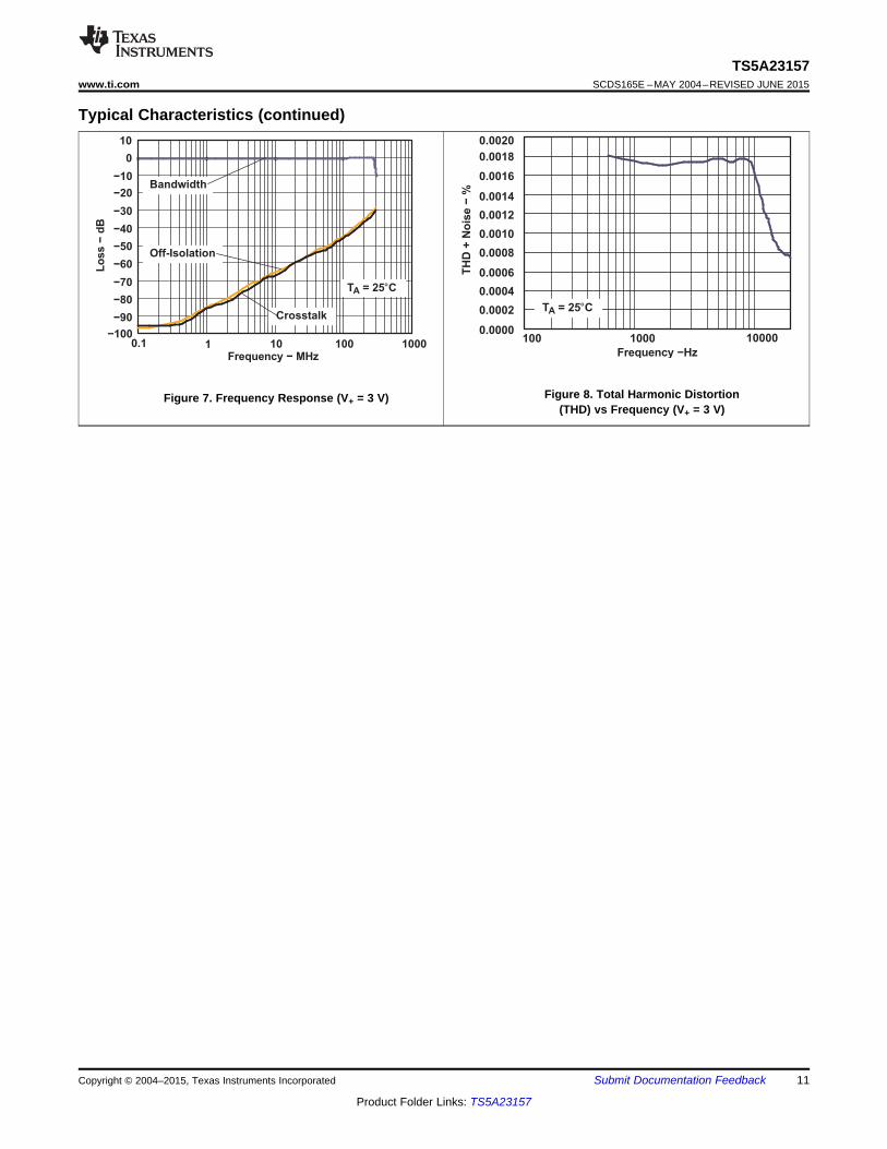
Typical Characteristics (continued)
Figure 8. Total Harmonic DistortionFigure 7. Frequency Response (V+ = 3 V)(THD) vs Frequency (V+ = 3 V)
Copyright © 2004–2015, Texas Instruments Incorporated Submit Documentation Feedback 11
Product Folder Links: TS5A23157
V+
GND
INVBIAS VIN
VIN = VIH or VIL
VBIAS = V+ or GND
Capacitance is measured at NC,
NO, COM, and IN inputs during
ON and OFF conditions.
Capacitance
Meter
VNO
VNC
VCOM
V+
GND
Channel OFF
NC
IN
VNC
VIN
NOCOM
VCOM
VCOM = 0 to V+
OFF-State Leakage Current
or
VIN = VIH or VIL
VNC or VNO = 0 to V+
Channel ON
VNC or VNO = Open, VCOM = 0 to V+
ON-State Leakage Current
or
VIN = VIH or VIL
VNC or VNO = 0 to V+, VCOM = Open
VNO
V+
ICOM
ron
VCOM
VNO /NC
ICOM
GND
Channel ON
NC
INVIN
NOCOM
VCOM
VIN = VIH or VIL
VNO
VNC
= Ω
TS5A23157SCDS165E –MAY 2004–REVISED JUNE 2015 www.ti.com
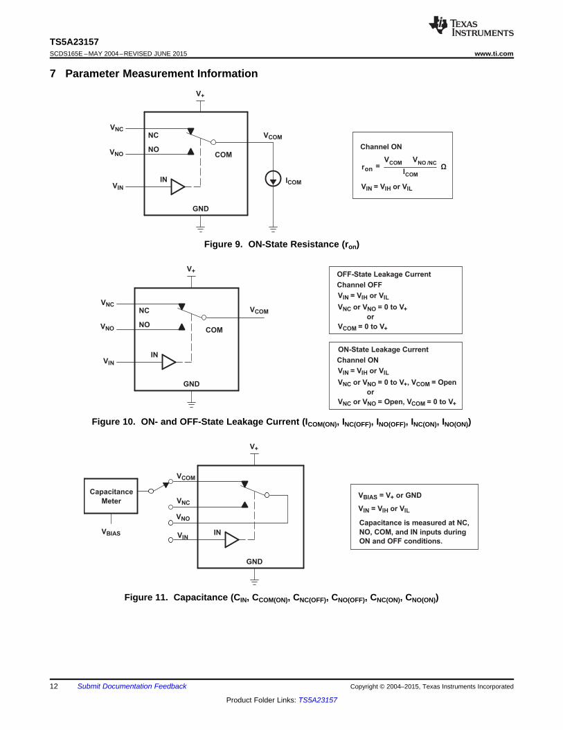
7 Parameter Measurement Information
Figure 9. ON-State Resistance (ron)
Figure 10. ON- and OFF-State Leakage Current (ICOM(ON), INC(OFF), INO(OFF), INC(ON), INO(ON))
Figure 11. Capacitance (CIN, CCOM(ON), CNC(OFF), CNO(OFF), CNC(ON), CNO(ON))
12 Submit Documentation Feedback Copyright © 2004–2015, Texas Instruments Incorporated
Product Folder Links: TS5A23157
V+
GND
NC
INVIN
NO
COM
50 Ω
50 Ω
VNC
VCOM
Gain = 20 logV
COM
VNC
dB
Channel ON: NC to COM
Network Analyzer Setup
Source Power = 0 dBM
DC Bias = 350 mV
Network Analyzer
Source
Signal
V+
GND
NC or NO
IN
VI
VIN
NC or NOCOM
VCOM
RL CLVCOM
tBBM
0
50%
90% 90%
VIN
tr < 5 ns
tf < 5 ns
VI = V+/2
RL = 50 Ω
CL = 35 pF
Logic
Input
Logic
Input
Switch
Output
V+
GND
NC or NO
IN
VNC or VNO
VIN
NC or NO COM
VCOM
RL CL
GND
V+
VNC
500 Ω
RL CL
50 pFV+
GND
VNO
tON
TEST
GND
V+500 Ω 50 pF
V+
GNDtOFF
50%
tON tOFF
VIN
VCOM
50%
90%
Logic
Input90%
Logic
Input
Switch
Output
TS5A23157www.ti.com SCDS165E –MAY 2004–REVISED JUNE 2015
Parameter Measurement Information (continued)
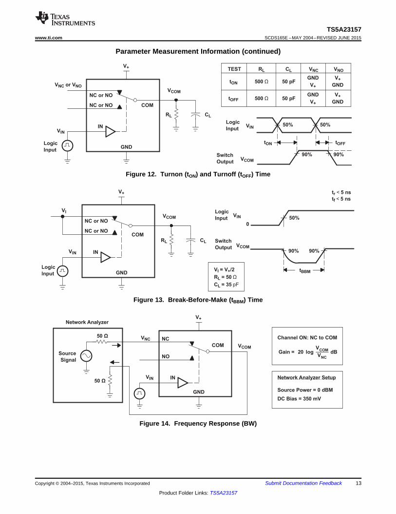
Figure 12. Turnon (tON) and Turnoff (tOFF) Time
Figure 13. Break-Before-Make (tBBM) Time
Figure 14. Frequency Response (BW)
Copyright © 2004–2015, Texas Instruments Incorporated Submit Documentation Feedback 13
Product Folder Links: TS5A23157
V+
GND
NC or NO
IN
RGEN
VIN
NC or NO COM
VOUT
RL CL
OFFVIN
VOUT
ON OFF
DVOUTVGEN
+
VIN = VIH or VIL
RL = 1 MΩ
CL = 35 pF
VGEN = 0
RGEN = 0
QC = CL × ΔVOUT
Logic
Input
VINH
VINL
Logic
Input
NC
NO
50 Ω
50 Ω
VNC
VCOMCrosstalk = 20 log
VNO
VNC
dB
Channel ON: NC to COM
Network Analyzer Setup
Source Power = 0 dBM
DC Bias = 350 mV
50 Ω
V+
GND
VNO
Source
Signal
Channel OFF: NO to COM
Network Analyzer
NC
NO
COM
VNC
VCOM OFF Isolation = 20 logV
COM
VNC
dB
Channel OFF: NC to COM
Network Analyzer Setup
Source Power = 0 dBM
DC Bias = 350 mV
50 Ω
V+
GND
50 Ω
50 Ω
Network Analyzer
Source
Signal
TS5A23157SCDS165E –MAY 2004–REVISED JUNE 2015 www.ti.com
Parameter Measurement Information (continued)
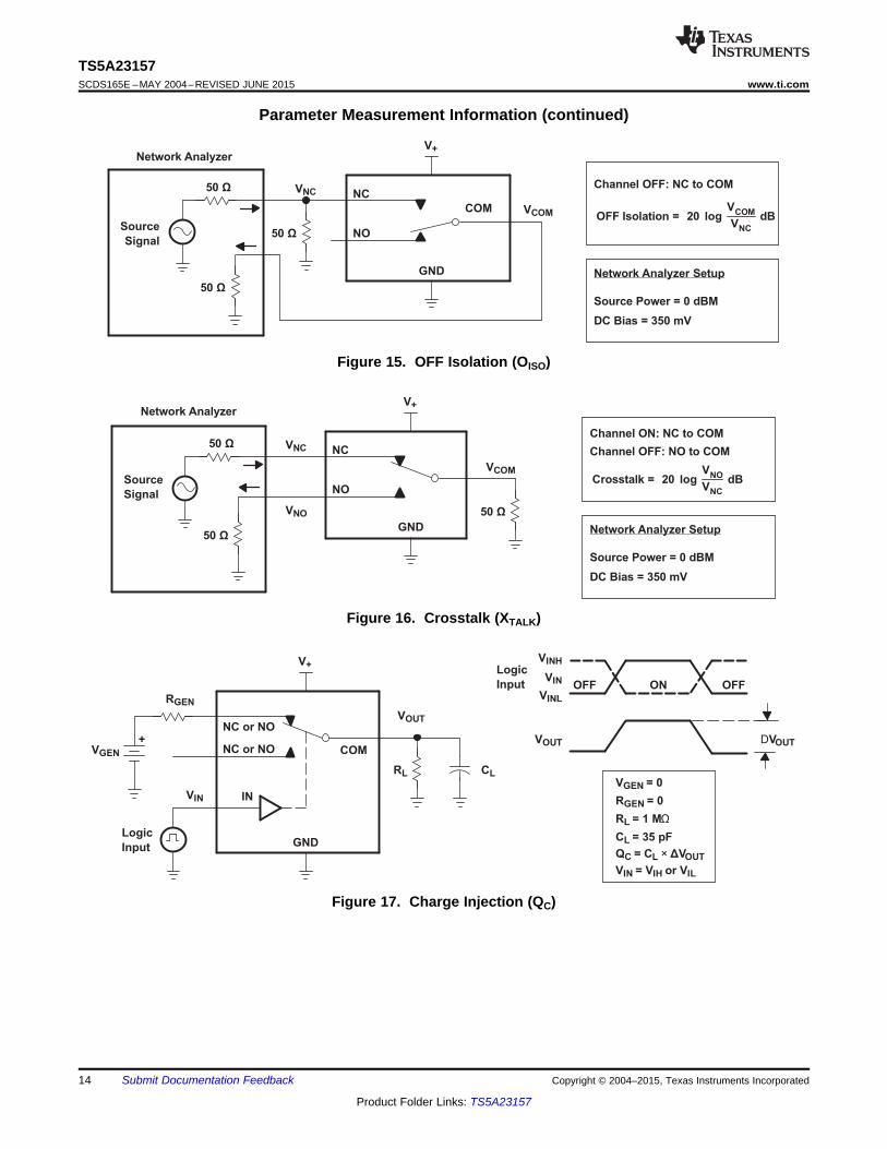
Figure 15. OFF Isolation (OISO)
Figure 16. Crosstalk (XTALK)
Figure 17. Charge Injection (QC)
14 Submit Documentation Feedback Copyright © 2004–2015, Texas Instruments Incorporated
Product Folder Links: TS5A23157
V+
GND
NC
NOCOM
10 µF
RL
CL
RL = 600 Ω
CL = 50 pF
VSOURCE = 0.5 V P-P
fSOURCE = 600 Hz to 20 kHzRL
VSOURCE
V+/2
Analyzer
10 µF
Channel ON: COM to NC
VO
TS5A23157www.ti.com SCDS165E –MAY 2004–REVISED JUNE 2015
Parameter Measurement Information (continued)
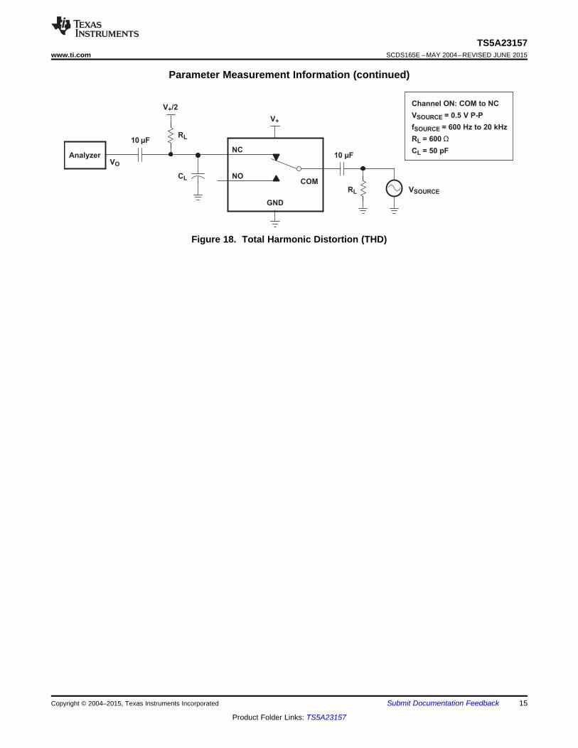
Figure 18. Total Harmonic Distortion (THD)
Copyright © 2004–2015, Texas Instruments Incorporated Submit Documentation Feedback 15
Product Folder Links: TS5A23157
NC1COM1
IN1
NO1
NC2COM2
IN2
NO2
TS5A23157SCDS165E –MAY 2004–REVISED JUNE 2015 www.ti.com
8 Detailed Description
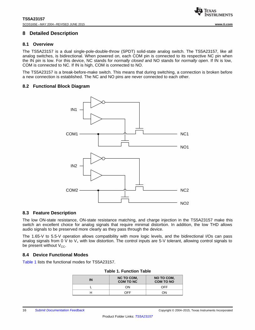
8.1 OverviewThe TS5A23157 is a dual single-pole-double-throw (SPDT) solid-state analog switch. The TS5A23157, like allanalog switches, is bidirectional. When powered on, each COM pin is connected to its respective NC pin whenthe IN pin is low. For this device, NC stands for normally closed and NO stands for normally open. If IN is low,COM is connected to NC. If IN is high, COM is connected to NO.
The TS5A23157 is a break-before-make switch. This means that during switching, a connection is broken beforea new connection is established. The NC and NO pins are never connected to each other.
8.2 Functional Block Diagram
8.3 Feature DescriptionThe low ON-state resistance, ON-state resistance matching, and charge injection in the TS5A23157 make thisswitch an excellent choice for analog signals that require minimal distortion. In addition, the low THD allowsaudio signals to be preserved more clearly as they pass through the device.
The 1.65-V to 5.5-V operation allows compatibility with more logic levels, and the bidirectional I/Os can passanalog signals from 0 V to V+ with low distortion. The control inputs are 5-V tolerant, allowing control signals tobe present without VCC.
8.4 Device Functional ModesTable 1 lists the functional modes for TS5A23157.
Table 1. Function TableNC TO COM, NO TO COM,IN COM TO NC COM TO NO
L ON OFFH OFF ON
16 Submit Documentation Feedback Copyright © 2004–2015, Texas Instruments Incorporated
Product Folder Links: TS5A23157
MCU or System Logic
1 COM1
NO1
NC1
GND
5 V
IN1
V+
To/From System 1
COM2
NO2
NC2
IN2
To/From System 2
MCU or System Logic
2
TS5A23157www.ti.com SCDS165E –MAY 2004–REVISED JUNE 2015
9 Application and Implementation
NOTEInformation in the following applications sections is not part of the TI componentspecification, and TI does not warrant its accuracy or completeness. TI’s customers areresponsible for determining suitability of components for their purposes. Customers shouldvalidate and test their design implementation to confirm system functionality.
9.1 Application InformationThe TS5A3157 can be used in a variety of customer systems. The TS5A3157 can be used anywhere multipleanalog or digital signals must be selected to pass across a single line.
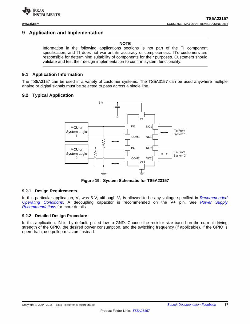
9.2 Typical Application
Figure 19. System Schematic for TS5A23157
9.2.1 Design RequirementsIn this particular application, V+ was 5 V, although V+ is allowed to be any voltage specified in RecommendedOperating Conditions. A decoupling capacitor is recommended on the V+ pin. See Power SupplyRecommendations for more details.
9.2.2 Detailed Design ProcedureIn this application, IN is, by default, pulled low to GND. Choose the resistor size based on the current drivingstrength of the GPIO, the desired power consumption, and the switching frequency (if applicable). If the GPIO isopen-drain, use pullup resistors instead.
Copyright © 2004–2015, Texas Instruments Incorporated Submit Documentation Feedback 17
Product Folder Links: TS5A23157
10
20
30
40
50
60
70
80
90
100
−60 −40 −20 0 20 40 60 80 1000
TA − Temperature − °C
I CC
+−
nA
TS5A23157SCDS165E –MAY 2004–REVISED JUNE 2015 www.ti.com
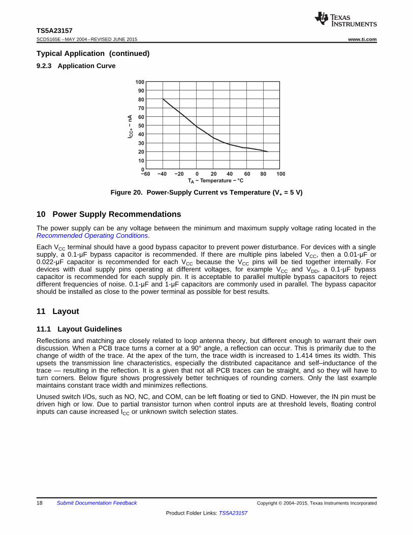
Typical Application (continued)9.2.3 Application Curve
Figure 20. Power-Supply Current vs Temperature (V+ = 5 V)
10 Power Supply RecommendationsThe power supply can be any voltage between the minimum and maximum supply voltage rating located in theRecommended Operating Conditions.
Each VCC terminal should have a good bypass capacitor to prevent power disturbance. For devices with a singlesupply, a 0.1-μF bypass capacitor is recommended. If there are multiple pins labeled VCC, then a 0.01-μF or0.022-μF capacitor is recommended for each VCC because the VCC pins will be tied together internally. Fordevices with dual supply pins operating at different voltages, for example VCC and VDD, a 0.1-µF bypasscapacitor is recommended for each supply pin. It is acceptable to parallel multiple bypass capacitors to rejectdifferent frequencies of noise. 0.1-μF and 1-μF capacitors are commonly used in parallel. The bypass capacitorshould be installed as close to the power terminal as possible for best results.
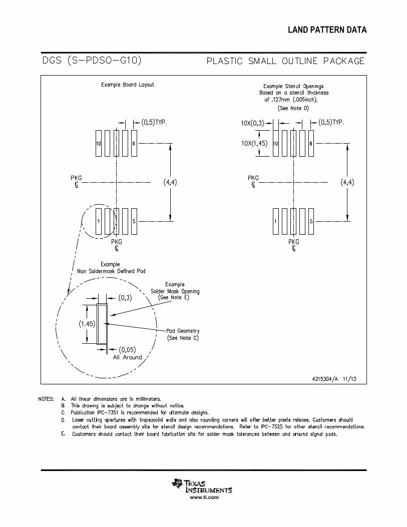
11 Layout
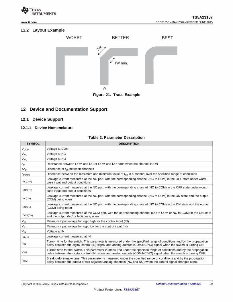
11.1 Layout GuidelinesReflections and matching are closely related to loop antenna theory, but different enough to warrant their owndiscussion. When a PCB trace turns a corner at a 90° angle, a reflection can occur. This is primarily due to thechange of width of the trace. At the apex of the turn, the trace width is increased to 1.414 times its width. Thisupsets the transmission line characteristics, especially the distributed capacitance and self–inductance of thetrace — resulting in the reflection. It is a given that not all PCB traces can be straight, and so they will have toturn corners. Below figure shows progressively better techniques of rounding corners. Only the last examplemaintains constant trace width and minimizes reflections.
Unused switch I/Os, such as NO, NC, and COM, can be left floating or tied to GND. However, the IN pin must bedriven high or low. Due to partial transistor turnon when control inputs are at threshold levels, floating controlinputs can cause increased ICC or unknown switch selection states.
18 Submit Documentation Feedback Copyright © 2004–2015, Texas Instruments Incorporated
Product Folder Links: TS5A23157
WORST BETTER BEST
1W min.
W
2W
TS5A23157www.ti.com SCDS165E –MAY 2004–REVISED JUNE 2015
11.2 Layout Example
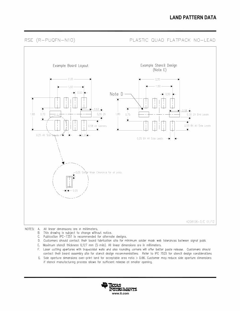
Figure 21. Trace Example
12 Device and Documentation Support
12.1 Device Support
12.1.1 Device Nomenclature
Table 2. Parameter DescriptionSYMBOL DESCRIPTION
VCOM Voltage at COMVNC Voltage at NCVNO Voltage at NOron Resistance between COM and NC or COM and NO ports when the channel is ONΔron Difference of ron between channelsron(flat) Difference between the maximum and minimum value of ron in a channel over the specified range of conditions
Leakage current measured at the NC port, with the corresponding channel (NC to COM) in the OFF state under worst-INC(OFF) case input and output conditionsLeakage current measured at the NO port, with the corresponding channel (NO to COM) in the OFF state under worst-INO(OFF) case input and output conditionsLeakage current measured at the NC port, with the corresponding channel (NC to COM) in the ON state and the outputINC(ON) (COM) being openLeakage current measured at the NO port, with the corresponding channel (NO to COM) in the ON state and the outputINO(ON) (COM) being openLeakage current measured at the COM port, with the corresponding channel (NO to COM or NC to COM) in the ON stateICOM(ON) and the output (NC or NO) being open
VIH Minimum input voltage for logic high for the control input (IN)VIL Minimum input voltage for logic low for the control input (IN)VIN Voltage at INIIH, IIL Leakage current measured at IN
Turnon time for the switch. This parameter is measured under the specified range of conditions and by the propagationtON delay between the digital control (IN) signal and analog outputs (COM/NC/NO) signal when the switch is turning ON.Turnoff time for the switch. This parameter is measured under the specified range of conditions and by the propagationtOFF delay between the digital control (IN) signal and analog outputs (COM/NC/NO) signal when the switch is turning OFF.Break-before-make time. This parameter is measured under the specified range of conditions and by the propagationtBBM delay between the output of two adjacent analog channels (NC and NO) when the control signal changes state.
Copyright © 2004–2015, Texas Instruments Incorporated Submit Documentation Feedback 19
Product Folder Links: TS5A23157
TS5A23157SCDS165E –MAY 2004–REVISED JUNE 2015 www.ti.com
Table 2. Parameter Description (continued)SYMBOL DESCRIPTION
Charge injection is a measurement of unwanted signal coupling from the control (IN) input to the analog (NC, NO, orCOM) output. This is measured in coulombs (C) and measured by the total charge induced due to switching of theQC control input. Charge injection, QC = CL× ΔVO, CL is the load capacitance and ΔVO is the change in analog outputvoltage.
CNC(OFF) Capacitance at the NC port when the corresponding channel (NC to COM) is OFFCNO(OFF) Capacitance at the NO port when the corresponding channel (NC to COM) is OFFCNC(ON) Capacitance at the NC port when the corresponding channel (NC to COM) is ONCNO(ON) Capacitance at the NO port when the corresponding channel (NC to COM) is ONCCOM(ON) Capacitance at the COM port when the corresponding channel (COM to NC or COM to NO) is ONCIN Capacitance of IN
OFF isolation of the switch is a measurement of OFF-state switch impedance. This is measured in dB in a specificOISO frequency, with the corresponding channel (NC to COM or NO to COM) in the OFF state. OFF isolation, OISO = 20 LOG
(VNC/VCOM) dB, VCOM is the input and VNC is the output.Crosstalk is a measurement of unwanted signal coupling from an ON channel to an OFF channel (NC to NO or NO to
XTALK NC). This is measured at a specific frequency and in dB. Crosstalk, XTALK = 20 log (VNC1/VNO1), VNO1 is the input andVNC1 is the output.Bandwidth of the switch. This is the frequency where the gain of an ON channel is –3 dB below the dc gain. Gain isBW measured from the equation, 20 log (VNC/VCOM) dB, where VNC is the output and VCOM is the input.
I+ Static power-supply current with the control (IN) pin at V+ or GNDΔI+ This is the increase in I+ for each control (IN) input that is at the specified voltage, rather than at V+ or GND.
Table 3. Summary of Characteristics2:1 MULTIPLEXER/DEMULTIPLEXERCONFIGURATION (2 × SPDT)
Number of channels 2ON-state resistance (ron) 10 ΩON-state resistance match between channels (Δron) 0.15 ΩON-state resistance flatness (ron(flat)) 4 ΩTurnon/turnoff time (tON/tOFF) 5.7 ns/3.8 nsBreak-before-make time (tBBM) 0.5 nsCharge injection (QC) 7 pCBandwidth (BW) 220 MHzOFF isolation (OSIO) –65 dB at 10 MHzCrosstalk 9XTALK) –66 dB at 10 MHzTotal harmo nic distortion (THD) 0.01%Leakage current (ICOM(OFF)/INC(OFF)) ±1 µAPackage options 10-pin DGS and RSE
20 Submit Documentation Feedback Copyright © 2004–2015, Texas Instruments Incorporated
Product Folder Links: TS5A23157
TS5A23157www.ti.com SCDS165E –MAY 2004–REVISED JUNE 2015
12.2 Documentation Support
12.2.1 Related DocumentationFor related documentation, see the following:• Implications of Slow or Floating CMOS Inputs, SCBA004
12.3 Community ResourcesThe following links connect to TI community resources. Linked contents are provided "AS IS" by the respectivecontributors. They do not constitute TI specifications and do not necessarily reflect TI's views; see TI's Terms ofUse.
TI E2E™ Online Community TI's Engineer-to-Engineer (E2E) Community. Created to foster collaborationamong engineers. At e2e.ti.com, you can ask questions, share knowledge, explore ideas and helpsolve problems with fellow engineers.
Design Support TI's Design Support Quickly find helpful E2E forums along with design support tools andcontact information for technical support.
12.4 TrademarksE2E is a trademark of Texas Instruments.All other trademarks are the property of their respective owners.
12.5 Electrostatic Discharge CautionThese devices have limited built-in ESD protection. The leads should be shorted together or the device placed in conductive foamduring storage or handling to prevent electrostatic damage to the MOS gates.
12.6 GlossarySLYZ022 — TI Glossary.
This glossary lists and explains terms, acronyms, and definitions.
13 Mechanical, Packaging, and Orderable InformationThe following pages include mechanical, packaging, and orderable information. This information is the mostcurrent data available for the designated devices. This data is subject to change without notice and revision ofthis document. For browser-based versions of this data sheet, refer to the left-hand navigation.
Copyright © 2004–2015, Texas Instruments Incorporated Submit Documentation Feedback 21
Product Folder Links: TS5A23157
PACKAGE OPTION ADDENDUM
www.ti.com 24-Aug-2018
Addendum-Page 1
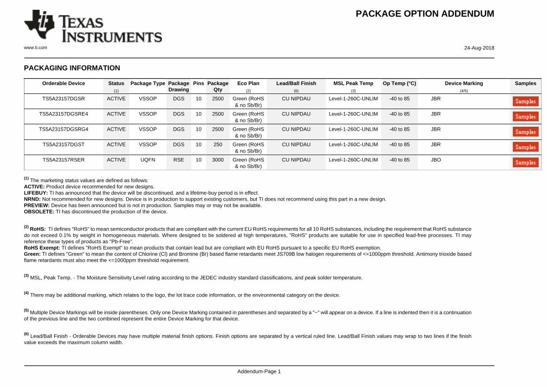
PACKAGING INFORMATION
Orderable Device Status(1)
Package Type PackageDrawing
Pins PackageQty
Eco Plan(2)
Lead/Ball Finish(6)
MSL Peak Temp(3)
Op Temp (°C) Device Marking(4/5)
Samples
TS5A23157DGSR ACTIVE VSSOP DGS 10 2500 Green (RoHS& no Sb/Br)
CU NIPDAU Level-1-260C-UNLIM -40 to 85 JBR
TS5A23157DGSRE4 ACTIVE VSSOP DGS 10 2500 Green (RoHS& no Sb/Br)
CU NIPDAU Level-1-260C-UNLIM -40 to 85 JBR
TS5A23157DGSRG4 ACTIVE VSSOP DGS 10 2500 Green (RoHS& no Sb/Br)
CU NIPDAU Level-1-260C-UNLIM -40 to 85 JBR
TS5A23157DGST ACTIVE VSSOP DGS 10 250 Green (RoHS& no Sb/Br)
CU NIPDAU Level-1-260C-UNLIM -40 to 85 JBR
TS5A23157RSER ACTIVE UQFN RSE 10 3000 Green (RoHS& no Sb/Br)
CU NIPDAU Level-1-260C-UNLIM -40 to 85 JBO
(1) The marketing status values are defined as follows:ACTIVE: Product device recommended for new designs.LIFEBUY: TI has announced that the device will be discontinued, and a lifetime-buy period is in effect.NRND: Not recommended for new designs. Device is in production to support existing customers, but TI does not recommend using this part in a new design.PREVIEW: Device has been announced but is not in production. Samples may or may not be available.OBSOLETE: TI has discontinued the production of the device.
(2) RoHS: TI defines "RoHS" to mean semiconductor products that are compliant with the current EU RoHS requirements for all 10 RoHS substances, including the requirement that RoHS substancedo not exceed 0.1% by weight in homogeneous materials. Where designed to be soldered at high temperatures, "RoHS" products are suitable for use in specified lead-free processes. TI mayreference these types of products as "Pb-Free".RoHS Exempt: TI defines "RoHS Exempt" to mean products that contain lead but are compliant with EU RoHS pursuant to a specific EU RoHS exemption.Green: TI defines "Green" to mean the content of Chlorine (Cl) and Bromine (Br) based flame retardants meet JS709B low halogen requirements of <=1000ppm threshold. Antimony trioxide basedflame retardants must also meet the <=1000ppm threshold requirement.
(3) MSL, Peak Temp. - The Moisture Sensitivity Level rating according to the JEDEC industry standard classifications, and peak solder temperature.
(4) There may be additional marking, which relates to the logo, the lot trace code information, or the environmental category on the device.
(5) Multiple Device Markings will be inside parentheses. Only one Device Marking contained in parentheses and separated by a "~" will appear on a device. If a line is indented then it is a continuationof the previous line and the two combined represent the entire Device Marking for that device.
(6) Lead/Ball Finish - Orderable Devices may have multiple material finish options. Finish options are separated by a vertical ruled line. Lead/Ball Finish values may wrap to two lines if the finishvalue exceeds the maximum column width.
PACKAGE OPTION ADDENDUM
www.ti.com 24-Aug-2018
Addendum-Page 2
Important Information and Disclaimer:The information provided on this page represents TI's knowledge and belief as of the date that it is provided. TI bases its knowledge and belief on informationprovided by third parties, and makes no representation or warranty as to the accuracy of such information. Efforts are underway to better integrate information from third parties. TI has taken andcontinues to take reasonable steps to provide representative and accurate information but may not have conducted destructive testing or chemical analysis on incoming materials and chemicals.TI and TI suppliers consider certain information to be proprietary, and thus CAS numbers and other limited information may not be available for release.
In no event shall TI's liability arising out of such information exceed the total purchase price of the TI part(s) at issue in this document sold by TI to Customer on an annual basis.
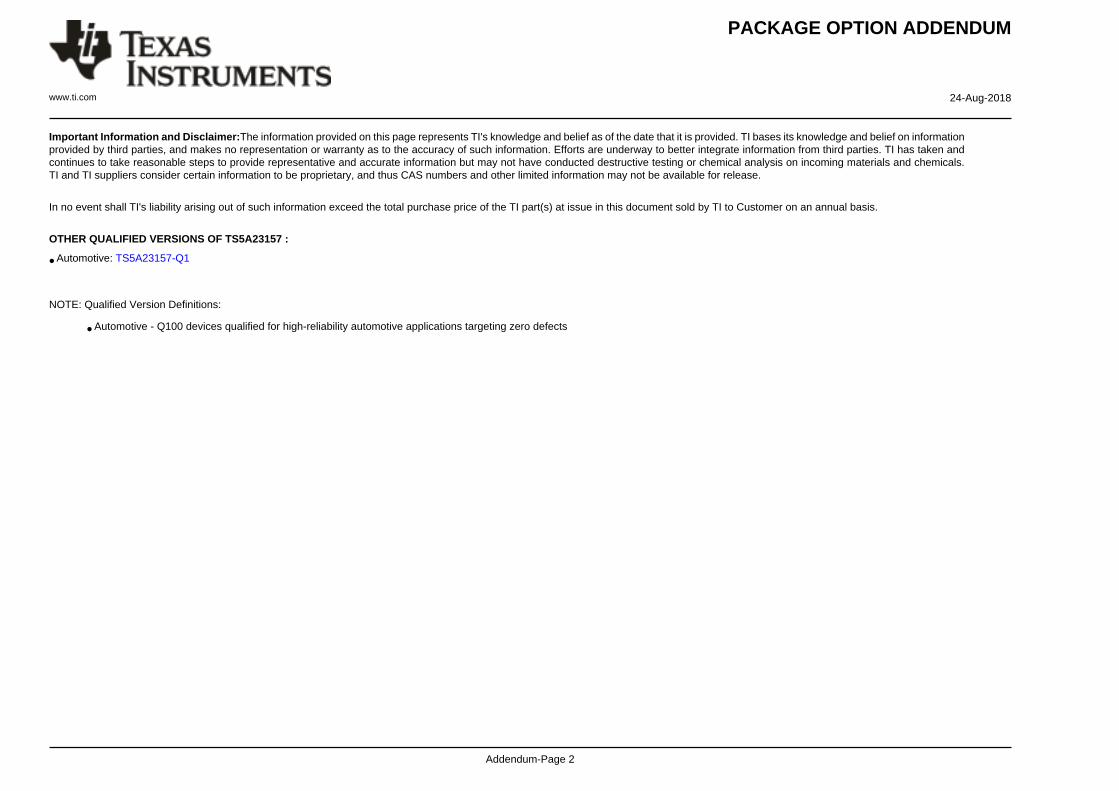
OTHER QUALIFIED VERSIONS OF TS5A23157 :
• Automotive: TS5A23157-Q1
NOTE: Qualified Version Definitions:
• Automotive - Q100 devices qualified for high-reliability automotive applications targeting zero defects
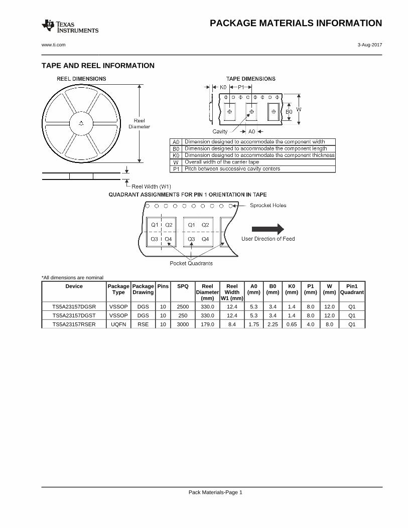
TAPE AND REEL INFORMATION
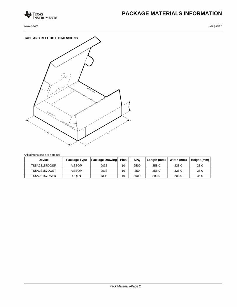
*All dimensions are nominal
Device PackageType
PackageDrawing
Pins SPQ ReelDiameter
(mm)
ReelWidth
W1 (mm)
A0(mm)
B0(mm)
K0(mm)
P1(mm)
W(mm)
Pin1Quadrant
TS5A23157DGSR VSSOP DGS 10 2500 330.0 12.4 5.3 3.4 1.4 8.0 12.0 Q1
TS5A23157DGST VSSOP DGS 10 250 330.0 12.4 5.3 3.4 1.4 8.0 12.0 Q1
TS5A23157RSER UQFN RSE 10 3000 179.0 8.4 1.75 2.25 0.65 4.0 8.0 Q1
PACKAGE MATERIALS INFORMATION
www.ti.com 3-Aug-2017
Pack Materials-Page 1
*All dimensions are nominal
Device Package Type Package Drawing Pins SPQ Length (mm) Width (mm) Height (mm)
TS5A23157DGSR VSSOP DGS 10 2500 358.0 335.0 35.0
TS5A23157DGST VSSOP DGS 10 250 358.0 335.0 35.0
TS5A23157RSER UQFN RSE 10 3000 203.0 203.0 35.0
PACKAGE MATERIALS INFORMATION
www.ti.com 3-Aug-2017
Pack Materials-Page 2
IMPORTANT NOTICE
Texas Instruments Incorporated (TI) reserves the right to make corrections, enhancements, improvements and other changes to itssemiconductor products and services per JESD46, latest issue, and to discontinue any product or service per JESD48, latest issue. Buyersshould obtain the latest relevant information before placing orders and should verify that such information is current and complete.TI’s published terms of sale for semiconductor products (http://www.ti.com/sc/docs/stdterms.htm) apply to the sale of packaged integratedcircuit products that TI has qualified and released to market. Additional terms may apply to the use or sale of other types of TI products andservices.Reproduction of significant portions of TI information in TI data sheets is permissible only if reproduction is without alteration and isaccompanied by all associated warranties, conditions, limitations, and notices. TI is not responsible or liable for such reproduceddocumentation. Information of third parties may be subject to additional restrictions. Resale of TI products or services with statementsdifferent from or beyond the parameters stated by TI for that product or service voids all express and any implied warranties for theassociated TI product or service and is an unfair and deceptive business practice. TI is not responsible or liable for any such statements.Buyers and others who are developing systems that incorporate TI products (collectively, “Designers”) understand and agree that Designersremain responsible for using their independent analysis, evaluation and judgment in designing their applications and that Designers havefull and exclusive responsibility to assure the safety of Designers' applications and compliance of their applications (and of all TI productsused in or for Designers’ applications) with all applicable regulations, laws and other applicable requirements. Designer represents that, withrespect to their applications, Designer has all the necessary expertise to create and implement safeguards that (1) anticipate dangerousconsequences of failures, (2) monitor failures and their consequences, and (3) lessen the likelihood of failures that might cause harm andtake appropriate actions. Designer agrees that prior to using or distributing any applications that include TI products, Designer willthoroughly test such applications and the functionality of such TI products as used in such applications.TI’s provision of technical, application or other design advice, quality characterization, reliability data or other services or information,including, but not limited to, reference designs and materials relating to evaluation modules, (collectively, “TI Resources”) are intended toassist designers who are developing applications that incorporate TI products; by downloading, accessing or using TI Resources in anyway, Designer (individually or, if Designer is acting on behalf of a company, Designer’s company) agrees to use any particular TI Resourcesolely for this purpose and subject to the terms of this Notice.TI’s provision of TI Resources does not expand or otherwise alter TI’s applicable published warranties or warranty disclaimers for TIproducts, and no additional obligations or liabilities arise from TI providing such TI Resources. TI reserves the right to make corrections,enhancements, improvements and other changes to its TI Resources. TI has not conducted any testing other than that specificallydescribed in the published documentation for a particular TI Resource.Designer is authorized to use, copy and modify any individual TI Resource only in connection with the development of applications thatinclude the TI product(s) identified in such TI Resource. NO OTHER LICENSE, EXPRESS OR IMPLIED, BY ESTOPPEL OR OTHERWISETO ANY OTHER TI INTELLECTUAL PROPERTY RIGHT, AND NO LICENSE TO ANY TECHNOLOGY OR INTELLECTUAL PROPERTYRIGHT OF TI OR ANY THIRD PARTY IS GRANTED HEREIN, including but not limited to any patent right, copyright, mask work right, orother intellectual property right relating to any combination, machine, or process in which TI products or services are used. Informationregarding or referencing third-party products or services does not constitute a license to use such products or services, or a warranty orendorsement thereof. Use of TI Resources may require a license from a third party under the patents or other intellectual property of thethird party, or a license from TI under the patents or other intellectual property of TI.TI RESOURCES ARE PROVIDED “AS IS” AND WITH ALL FAULTS. TI DISCLAIMS ALL OTHER WARRANTIES ORREPRESENTATIONS, EXPRESS OR IMPLIED, REGARDING RESOURCES OR USE THEREOF, INCLUDING BUT NOT LIMITED TOACCURACY OR COMPLETENESS, TITLE, ANY EPIDEMIC FAILURE WARRANTY AND ANY IMPLIED WARRANTIES OFMERCHANTABILITY, FITNESS FOR A PARTICULAR PURPOSE, AND NON-INFRINGEMENT OF ANY THIRD PARTY INTELLECTUALPROPERTY RIGHTS. TI SHALL NOT BE LIABLE FOR AND SHALL NOT DEFEND OR INDEMNIFY DESIGNER AGAINST ANY CLAIM,INCLUDING BUT NOT LIMITED TO ANY INFRINGEMENT CLAIM THAT RELATES TO OR IS BASED ON ANY COMBINATION OFPRODUCTS EVEN IF DESCRIBED IN TI RESOURCES OR OTHERWISE. IN NO EVENT SHALL TI BE LIABLE FOR ANY ACTUAL,DIRECT, SPECIAL, COLLATERAL, INDIRECT, PUNITIVE, INCIDENTAL, CONSEQUENTIAL OR EXEMPLARY DAMAGES INCONNECTION WITH OR ARISING OUT OF TI RESOURCES OR USE THEREOF, AND REGARDLESS OF WHETHER TI HAS BEENADVISED OF THE POSSIBILITY OF SUCH DAMAGES.Unless TI has explicitly designated an individual product as meeting the requirements of a particular industry standard (e.g., ISO/TS 16949and ISO 26262), TI is not responsible for any failure to meet such industry standard requirements.Where TI specifically promotes products as facilitating functional safety or as compliant with industry functional safety standards, suchproducts are intended to help enable customers to design and create their own applications that meet applicable functional safety standardsand requirements. Using products in an application does not by itself establish any safety features in the application. Designers mustensure compliance with safety-related requirements and standards applicable to their applications. Designer may not use any TI products inlife-critical medical equipment unless authorized officers of the parties have executed a special contract specifically governing such use.Life-critical medical equipment is medical equipment where failure of such equipment would cause serious bodily injury or death (e.g., lifesupport, pacemakers, defibrillators, heart pumps, neurostimulators, and implantables). Such equipment includes, without limitation, allmedical devices identified by the U.S. Food and Drug Administration as Class III devices and equivalent classifications outside the U.S.TI may expressly designate certain products as completing a particular qualification (e.g., Q100, Military Grade, or Enhanced Product).Designers agree that it has the necessary expertise to select the product with the appropriate qualification designation for their applicationsand that proper product selection is at Designers’ own risk. Designers are solely responsible for compliance with all legal and regulatoryrequirements in connection with such selection.Designer will fully indemnify TI and its representatives against any damages, costs, losses, and/or liabilities arising out of Designer’s non-compliance with the terms and provisions of this Notice.
Mailing Address: Texas Instruments, Post Office Box 655303, Dallas, Texas 75265Copyright © 2018, Texas Instruments Incorporated