TS3A24157 0.65-Ω2-Channel SPDT Analog Switch 2 Changed V+ pin name to VCC..... 3 • Added...
28
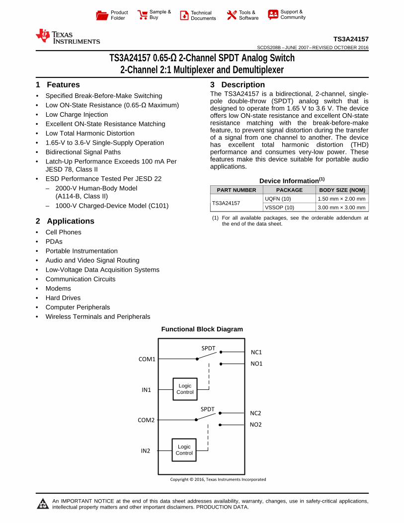
IN1 COM1 NC1 NO1 SPDT Logic Control IN2 COM2 NC2 NO2 SPDT Logic Control Copyright ' 2016, Texas Instruments Incorporated Product Folder Sample & Buy Technical Documents Tools & Software Support & Community An IMPORTANT NOTICE at the end of this data sheet addresses availability, warranty, changes, use in safety-critical applications, intellectual property matters and other important disclaimers. PRODUCTION DATA. TS3A24157 SCDS208B – JUNE 2007 – REVISED OCTOBER 2016 TS3A24157 0.65-Ω 2-Channel SPDT Analog Switch 2-Channel 2:1 Multiplexer and Demultiplexer 1 1 Features 1• Specified Break-Before-Make Switching • Low ON-State Resistance (0.65-Ω Maximum) • Low Charge Injection • Excellent ON-State Resistance Matching • Low Total Harmonic Distortion • 1.65-V to 3.6-V Single-Supply Operation • Bidirectional Signal Paths • Latch-Up Performance Exceeds 100 mA Per JESD 78, Class II • ESD Performance Tested Per JESD 22 – 2000-V Human-Body Model (A114-B, Class II) – 1000-V Charged-Device Model (C101) 2 Applications • Cell Phones • PDAs • Portable Instrumentation • Audio and Video Signal Routing • Low-Voltage Data Acquisition Systems • Communication Circuits • Modems • Hard Drives • Computer Peripherals • Wireless Terminals and Peripherals 3 Description The TS3A24157 is a bidirectional, 2-channel, single- pole double-throw (SPDT) analog switch that is designed to operate from 1.65 V to 3.6 V. The device offers low ON-state resistance and excellent ON-state resistance matching with the break-before-make feature, to prevent signal distortion during the transfer of a signal from one channel to another. The device has excellent total harmonic distortion (THD) performance and consumes very-low power. These features make this device suitable for portable audio applications. Device Information (1) PART NUMBER PACKAGE BODY SIZE (NOM) TS3A24157 UQFN (10) 1.50 mm × 2.00 mm VSSOP (10) 3.00 mm × 3.00 mm (1) For all available packages, see the orderable addendum at the end of the data sheet. Functional Block Diagram
Transcript of TS3A24157 0.65-Ω2-Channel SPDT Analog Switch 2 Changed V+ pin name to VCC..... 3 • Added...
IN1
COM1NC1
NO1
SPDT
Logic Control
IN2
COM2NC2
NO2
SPDT
Logic Control
Copyright © 2016, Texas Instruments Incorporated
Product
Folder
Sample &Buy
Technical
Documents
Tools &
Software
Support &Community
An IMPORTANT NOTICE at the end of this data sheet addresses availability, warranty, changes, use in safety-critical applications,intellectual property matters and other important disclaimers. PRODUCTION DATA.
TS3A24157SCDS208B –JUNE 2007–REVISED OCTOBER 2016
TS3A24157 0.65-Ω 2-Channel SPDT Analog Switch2-Channel 2:1 Multiplexer and Demultiplexer
1
1 Features1• Specified Break-Before-Make Switching• Low ON-State Resistance (0.65-Ω Maximum)• Low Charge Injection• Excellent ON-State Resistance Matching• Low Total Harmonic Distortion• 1.65-V to 3.6-V Single-Supply Operation• Bidirectional Signal Paths• Latch-Up Performance Exceeds 100 mA Per
JESD 78, Class II• ESD Performance Tested Per JESD 22
– 2000-V Human-Body Model(A114-B, Class II)
– 1000-V Charged-Device Model (C101)
2 Applications• Cell Phones• PDAs• Portable Instrumentation• Audio and Video Signal Routing• Low-Voltage Data Acquisition Systems• Communication Circuits• Modems• Hard Drives• Computer Peripherals• Wireless Terminals and Peripherals
3 DescriptionThe TS3A24157 is a bidirectional, 2-channel, single-pole double-throw (SPDT) analog switch that isdesigned to operate from 1.65 V to 3.6 V. The deviceoffers low ON-state resistance and excellent ON-stateresistance matching with the break-before-makefeature, to prevent signal distortion during the transferof a signal from one channel to another. The devicehas excellent total harmonic distortion (THD)performance and consumes very-low power. Thesefeatures make this device suitable for portable audioapplications.
Device Information(1)
PART NUMBER PACKAGE BODY SIZE (NOM)
TS3A24157UQFN (10) 1.50 mm × 2.00 mmVSSOP (10) 3.00 mm × 3.00 mm
(1) For all available packages, see the orderable addendum atthe end of the data sheet.
Functional Block Diagram
2
TS3A24157SCDS208B –JUNE 2007–REVISED OCTOBER 2016 www.ti.com
Product Folder Links: TS3A24157
Submit Documentation Feedback Copyright © 2007–2016, Texas Instruments Incorporated
Table of Contents1 Features .................................................................. 12 Applications ........................................................... 13 Description ............................................................. 14 Revision History..................................................... 25 Pin Configuration and Functions ......................... 36 Specifications......................................................... 4
6.1 Absolute Maximum Ratings ...................................... 46.2 ESD Ratings.............................................................. 46.3 Recommended Operating Conditions....................... 46.4 Thermal Information .................................................. 46.5 Electrical Characteristics: 3-V Supply ...................... 56.6 Electrical Characteristics: 2.5-V Supply .................... 66.7 Electrical Characteristics: 1.8-V Supply .................... 76.8 Typical Characteristics .............................................. 8
7 Parameter Measurement Information ................ 108 Detailed Description ............................................ 14
8.1 Overview ................................................................. 148.2 Functional Block Diagram ....................................... 14
8.3 Feature Description................................................. 148.4 Device Functional Modes........................................ 14
9 Application and Implementation ........................ 159.1 Application Information............................................ 159.2 Typical Application .................................................. 15
10 Power Supply Recommendations ..................... 1611 Layout................................................................... 16
11.1 Layout Guidelines ................................................. 1611.2 Layout Example .................................................... 16
12 Device and Documentation Support ................. 1712.1 Device Support...................................................... 1712.2 Documentation Support ........................................ 1812.3 Receiving Notification of Documentation Updates 1812.4 Community Resources.......................................... 1812.5 Trademarks ........................................................... 1812.6 Electrostatic Discharge Caution............................ 1812.7 Glossary ................................................................ 18
13 Mechanical, Packaging, and OrderableInformation ........................................................... 19
4 Revision HistoryNOTE: Page numbers for previous revisions may differ from page numbers in the current version.
Changes from Revision A (September 2007) to Revision B Page
• Added ESD Ratings table, Feature Description section, Device Functional Modes, Application and Implementationsection, Power Supply Recommendations section, Layout section, Device and Documentation Support section, andMechanical, Packaging, and Orderable Information section. ................................................................................................. 1
• Deleted Ordering Information table; see POA at the end of the data sheet........................................................................... 1• Deleted Summary of Characteristics table ............................................................................................................................. 1• Changed V+ pin name to VCC................................................................................................................................................ 3• Added Thermal Information table ........................................................................................................................................... 4
1NC1
2NO1
3NC2
4NO2
5G
ND
6 COM2
7 IN2
8 IN1
9 COM1
10
VC
C
Not to scale
1NC1 10 VCC
2NO1 9 COM1
3NC2 8 IN1
4NO2 7 IN2
5GND 6 COM2
Not to scale
3
TS3A24157www.ti.com SCDS208B –JUNE 2007–REVISED OCTOBER 2016
Product Folder Links: TS3A24157
Submit Documentation FeedbackCopyright © 2007–2016, Texas Instruments Incorporated
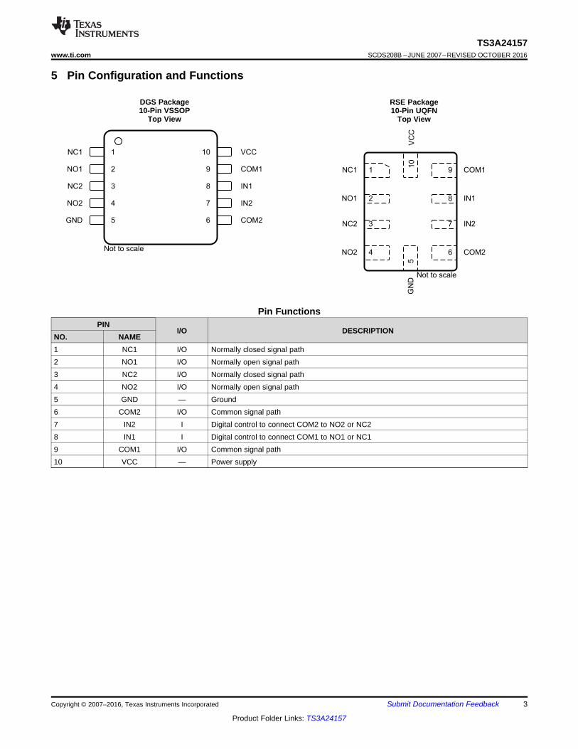
5 Pin Configuration and Functions
DGS Package10-Pin VSSOP
Top View
RSE Package10-Pin UQFN
Top View
Pin FunctionsPIN
I/O DESCRIPTIONNO. NAME1 NC1 I/O Normally closed signal path2 NO1 I/O Normally open signal path3 NC2 I/O Normally closed signal path4 NO2 I/O Normally open signal path5 GND — Ground6 COM2 I/O Common signal path7 IN2 I Digital control to connect COM2 to NO2 or NC28 IN1 I Digital control to connect COM1 to NO1 or NC19 COM1 I/O Common signal path10 VCC — Power supply
4
TS3A24157SCDS208B –JUNE 2007–REVISED OCTOBER 2016 www.ti.com
Product Folder Links: TS3A24157
Submit Documentation Feedback Copyright © 2007–2016, Texas Instruments Incorporated
(1) Stresses beyond those listed under Absolute Maximum Ratings may cause permanent damage to the device. These are stress ratingsonly, which do not imply functional operation of the device at these or any other conditions beyond those indicated under RecommendedOperating Conditions. Exposure to absolute-maximum-rated conditions for extended periods may affect device reliability.
(2) All voltages are with respect to ground, unless otherwise specified.(3) The algebraic convention, whereby the most negative value is a minimum and the most positive value is a maximum.(4) This value is limited to 5.5 V (maximum).(5) Pulse at 1-ms duration < 10% duty cycle.
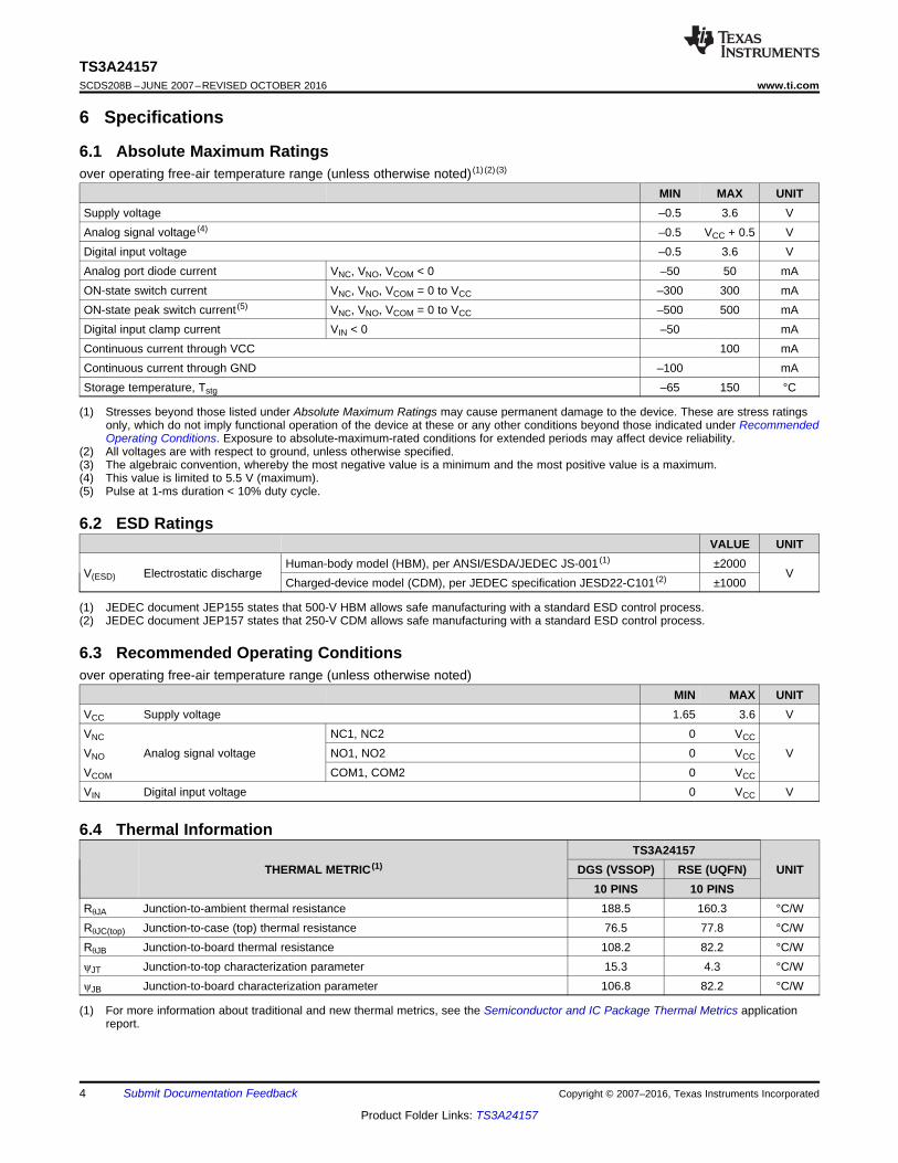
6 Specifications
6.1 Absolute Maximum Ratingsover operating free-air temperature range (unless otherwise noted) (1) (2) (3)
MIN MAX UNITSupply voltage –0.5 3.6 VAnalog signal voltage (4) –0.5 VCC + 0.5 VDigital input voltage –0.5 3.6 VAnalog port diode current VNC, VNO, VCOM < 0 –50 50 mAON-state switch current VNC, VNO, VCOM = 0 to VCC –300 300 mAON-state peak switch current (5) VNC, VNO, VCOM = 0 to VCC –500 500 mADigital input clamp current VIN < 0 –50 mAContinuous current through VCC 100 mAContinuous current through GND –100 mAStorage temperature, Tstg –65 150 °C
(1) JEDEC document JEP155 states that 500-V HBM allows safe manufacturing with a standard ESD control process.(2) JEDEC document JEP157 states that 250-V CDM allows safe manufacturing with a standard ESD control process.
6.2 ESD RatingsVALUE UNIT
V(ESD) Electrostatic dischargeHuman-body model (HBM), per ANSI/ESDA/JEDEC JS-001 (1) ±2000
VCharged-device model (CDM), per JEDEC specification JESD22-C101 (2) ±1000
6.3 Recommended Operating Conditionsover operating free-air temperature range (unless otherwise noted)
MIN MAX UNITVCC Supply voltage 1.65 3.6 VVNC
Analog signal voltageNC1, NC2 0 VCC
VVNO NO1, NO2 0 VCC
VCOM COM1, COM2 0 VCC
VIN Digital input voltage 0 VCC V
(1) For more information about traditional and new thermal metrics, see the Semiconductor and IC Package Thermal Metrics applicationreport.
6.4 Thermal Information
THERMAL METRIC (1)TS3A24157
UNITDGS (VSSOP) RSE (UQFN)10 PINS 10 PINS
RθJA Junction-to-ambient thermal resistance 188.5 160.3 °C/WRθJC(top) Junction-to-case (top) thermal resistance 76.5 77.8 °C/WRθJB Junction-to-board thermal resistance 108.2 82.2 °C/WψJT Junction-to-top characterization parameter 15.3 4.3 °C/WψJB Junction-to-board characterization parameter 106.8 82.2 °C/W
5
TS3A24157www.ti.com SCDS208B –JUNE 2007–REVISED OCTOBER 2016
Product Folder Links: TS3A24157
Submit Documentation FeedbackCopyright © 2007–2016, Texas Instruments Incorporated
(1) All unused digital inputs of the device must be held at VCCor GND to ensure proper device operation. See Implications of Slow orFloating CMOS Inputs.
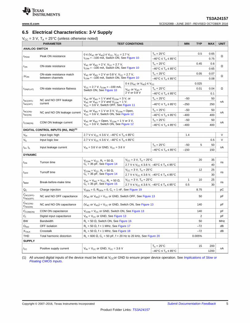
6.5 Electrical Characteristics: 3-V SupplyVCC = 3 V, TA = 25°C (unless otherwise noted)
PARAMETER TEST CONDITIONS MIN TYP MAX UNIT
ANALOG SWITCH
rPEAK Peak ON resistance 0 ≤ (VNC or VNO) ≤ VCC, VCC = 2.7 V,ICOM = –100 mA, Switch ON, See Figure 10
TA = 25°C 0.5 0.65Ω
–40°C ≤ TA ≤ 85°C 0.75
rON ON-state resistance VNC or VNO = 2 V, VCC = 2.7 V,ICOM = –100 mA, Switch ON, See Figure 10
TA = 25°C 0.45 0.6Ω
–40°C ≤ TA ≤ 85°C 0.65
ΔrONON-state resistance matchbetween channels
VNC or VNO = 2 V or 0.8 V, VCC = 2.7 V,ICOM = –100 mA, Switch ON, See Figure 10
TA = 25°C 0.05 0.07Ω
–40°C ≤ TA ≤ 85°C 0.08
rON(FLAT) ON-state resistance flatness VCC = 2.7 V, ICOM = –100 mA,Switch ON, See Figure 10
0 ≤ (VNC or VNO) ≤ VCC 0.025
ΩVNC or VNO =2 V or 0.8 V
TA = 25°C 0.01 0.04
–40°C ≤ TA ≤ 85°C 0.1
INC(OFF),INO(OFF)
NC and NO OFF leakagecurrent
VNC or VNO = 1 V and VCOM = 3 V, orVNC or VNO = 3 V and VCOM = 1 V;VCC = 3.6 V, Switch OFF, See Figure 11
TA = 25°C –50 50nA
–40°C ≤ TA ≤ 85°C –250 250
INC(ON),INO(ON)
NC and NO ON leakage current VNC or VNO = 1 V or 3 V, VCOM = Open,VCC = 3.6 V, Switch ON, See Figure 12
TA = 25°C –50 50nA
–40°C ≤ TA ≤ 85°C –400 400
ICOM(ON) COM ON leakage current VNC or VNO = Open, VCOM = 1 V or 3 V,VCC = 3.6 V, Switch ON, See Figure 12
TA = 25°C –50 50nA
–40°C ≤ TA ≤ 85°C –400 400
DIGITAL CONTROL INPUTS (IN1, IN2) (1)
VIH Input logic high 2.7 V ≤ VCC ≤ 3.6 V, –40°C ≤ TA ≤ 85°C 1.4 V
VIL Input logic low 2.7 V ≤ VCC ≤ 3.6 V, –40°C ≤ TA ≤ 85°C 0.5 V
IIH, IIL Input leakage current VIN = 3.6 V or GND, VCC = 3.6 VTA = 25°C –50 5 50
nA–40°C ≤ TA ≤ 85°C –150 150
DYNAMIC
tON Turnon time VCOM = VCC, RL = 50 Ω,CL = 35 pF, See Figure 14
VCC = 3 V, TA = 25°C 20 35ns
2.7 V ≤ VCC ≤ 3.6 V, –40°C ≤ TA ≤ 85°C 40
tOFF Turnoff time VCOM = VCC, RL = 50 Ω,CL = 35 pF, See Figure 14
VCC = 3 V, TA = 25°C 12 25ns
2.7 V ≤ VCC ≤ 3.6 V, –40°C ≤ TA ≤ 85°C 30
tBBM Break-before-make time VNC = VNO = VCC, RL = 50 Ω,CL = 35 pF, See Figure 15
VCC = 3 V, TA = 25°C 1 10 25ns
2.7 V ≤ VCC ≤ 3.6 V, –40°C ≤ TA ≤ 85°C 0.5 30
QC Charge injection VGEN = 0, RGEN = 0, CL = 1 nF, See Figure 19 8.75 pC
CNC(OFF),CNO(OFF)
NC and NO OFF capacitance (VNC or VNO) = VCC or GND, Switch OFF, See Figure 13 50 pF
CNC(ON),CNO(ON)
NC and NO ON capacitance (VNC or VNO) = VCC or GND, Switch ON, See Figure 13 140 pF
CCOM(ON) COM ON capacitance VCOM = VCC or GND, Switch ON, See Figure 13 140 pF
CI Digital input capacitance VIN = VCC or GND, See Figure 13 2 pF
BW Bandwidth RL = 50 Ω, Switch ON, See Figure 16 50 MHz
OISO OFF isolation RL = 50 Ω, f = 1 MHz, See Figure 17 –72 dB
XTALK Crosstalk RL = 50 Ω, f = 1 MHz, See Figure 18 –72 dB
THD Total harmonic distortion RL = 600 Ω, CL = 50 pF, f = 20 Hz to 20 kHz, See Figure 20 0.005%
SUPPLY
ICC Positive supply current VIN = VCC or GND, VCC = 3.6 VTA = 25°C 15 200
nA–40°C ≤ TA ≤ 85°C 1200
6
TS3A24157SCDS208B –JUNE 2007–REVISED OCTOBER 2016 www.ti.com
Product Folder Links: TS3A24157
Submit Documentation Feedback Copyright © 2007–2016, Texas Instruments Incorporated
(1) All unused digital inputs of the device must be held at VCCor GND to ensure proper device operation. See Implications of Slow orFloating CMOS Inputs.
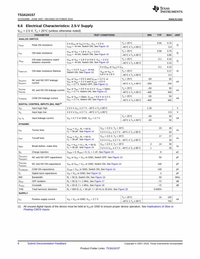
6.6 Electrical Characteristics: 2.5-V SupplyVCC = 2.5 V, TA = 25°C (unless otherwise noted)
PARAMETER TEST CONDITIONS MIN TYP MAX UNIT
ANALOG SWITCH
rPEAK Peak ON resistance 0 ≤ (VNO or VNC) ≤ VCC, VCC = 2.3 V,ICOM = –8 mA, Switch ON, See Figure 10
TA = 25°C 0.55 0.75Ω
–40°C ≤ TA ≤ 85°C 0.9
rON ON-state resistance VNO or VNC = 1.8 V, VCC = 2.3 V,ICOM = –8 mA, Switch ON, See Figure 10
TA = 25°C 0.56 0.75Ω
–40°C ≤ TA ≤ 85°C 0.85
ΔrONON-state resistance matchbetween channels
VNO or VNC = 1.8 V or 0.8 V, VCC = 2.3 V,ICOM = –8 mA, Switch ON, See Figure 10
TA = 25°C 0.1 0.15Ω
–40°C ≤ TA ≤ 85°C 0.15
rON(FLAT) ON-state resistance flatness VCC = 2.3 V, ICOM = –8 mA,Switch ON, See Figure 10
0 ≤ (VNO or VNC) ≤ VCC 0.1 0.15
ΩVNO or VNC =0.8 V or 1.8 V
TA = 25°C 0.17
–40°C ≤ TA ≤ 85°C 0.2
INC(OFF),INO(OFF)
NC and NO OFF leakagecurrent
VNC or VNO = 0.5 V and VCOM = 2.2 V, orVNC or VNO = 2.2 V and VCOM = 0.5 V;VCC = 2.7 V, Switch OFF, See Figure 11
TA = 25°C –50 50nA
–40°C ≤ TA ≤ 85°C –250 250
INC(ON),INO(ON)
NC and NO ON leakage current VNC or VNO = 0.5 V or 2.2 V, VCOM = Open,VCC = 2.7 V, Switch ON, See Figure 12
TA = 25°C –50 50nA
–40°C ≤ TA ≤ 85°C –400 400
ICOM(ON) COM ON leakage current VNC or VNO = Open, VCOM = 0.5 V or 2.2 V,VCC = 2.7 V, Switch ON, See Figure 12
TA = 25°C –50 50nA
–40°C ≤ TA ≤ 85°C –400 400
DIGITAL CONTROL INPUTS (IN1, IN2) (1)
VIH Input logic high 2.3 V ≤ VCC ≤ 2.7 V, –40°C ≤ TA ≤ 85°C 1.25 V
VIL Input logic low 2.3 V ≤ VCC ≤ 2.7 V, –40°C ≤ TA ≤ 85°C 0.5 V
IIH, IIL Input leakage current VIN = 2.7 V or GND, VCC = 2.7 VTA = 25°C –50 50
nA–40°C ≤ TA ≤ 85°C –50 50
DYNAMIC
tON Turnon time VCOM = VCC, RL = 50 Ω,CL = 35 pF, See Figure 14
VCC = 2.5 V, TA = 25°C 23 45ns
2.3 V ≤ VCC ≤ 2.7 V, –40°C ≤ TA ≤ 85°C 50
tOFF Turnoff time VCOM = VCC, RL = 50 Ω,CL = 35 pF, See Figure 14
VCC = 2.5 V, TA = 25°C 17 27ns
2.3 V ≤ VCC ≤ 2.7 V, –40°C ≤ TA ≤ 85°C 30
tBBM Break-before- make time VNC = VNO = VCC, RL = 50 Ω,CL = 35 pF, See Figure 15
VCC = 2.5 V, TA = 25°C 2 14 30ns
2.3 V ≤ VCC ≤ 2.7 V, –40°C ≤ TA ≤ 85°C 1 35
QC Charge injection VGEN = 0, RGEN = 0, CL = 1 nF, See Figure 19 8 pC
CNC(OFF),CNO(OFF)
NC and NO OFF capacitance VNC or VNO = VCC or GND, Switch OFF, See Figure 13 50 pF
CNC(ON),CNO(ON)
NC and NO ON capacitance VNC or VNO = VCC or GND, Switch ON, See Figure 13 140 pF
CCOM(ON) COM ON capacitance VCOM = VCC or GND, Switch ON, See Figure 13 140 pF
CI Digital input capacitance VIN = VCC or GND, See Figure 13 2 pF
BW Bandwidth RL = 50 Ω, Switch ON, See Figure 16 50 MHz
OISO OFF isolation RL = 50 Ω, f = 1 MHz, See Figure 17 –72 dB
XTALK Crosstalk RL = 50 Ω, f = 1 MHz, See Figure 18 –72 dB
THD Total harmonic distortion RL = 600 Ω, CL = 50 pF, f = 20 Hz to 20 kHz, See Figure 20 0.006%
SUPPLY
ICC Positive supply current VIN = VCC or GND, VCC = 2.7 VTA = 25°C 10 150
nA–40°C ≤ TA ≤ 85°C 700
7
TS3A24157www.ti.com SCDS208B –JUNE 2007–REVISED OCTOBER 2016
Product Folder Links: TS3A24157
Submit Documentation FeedbackCopyright © 2007–2016, Texas Instruments Incorporated
(1) All unused digital inputs of the device must be held at VCCor GND to ensure proper device operation. See Implications of Slow orFloating CMOS Inputs.
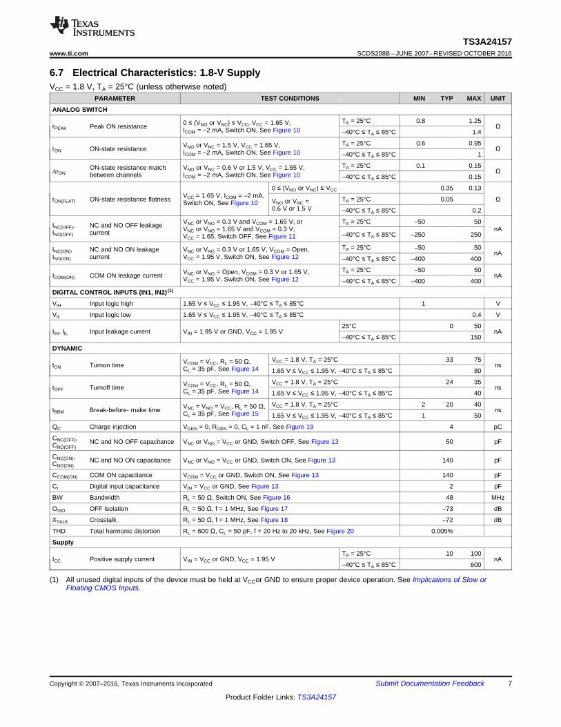
6.7 Electrical Characteristics: 1.8-V SupplyVCC = 1.8 V, TA = 25°C (unless otherwise noted)
PARAMETER TEST CONDITIONS MIN TYP MAX UNIT
ANALOG SWITCH
rPEAK Peak ON resistance 0 ≤ (VNO or VNC) ≤ VCC, VCC = 1.65 V,ICOM = –2 mA, Switch ON, See Figure 10
TA = 25°C 0.8 1.25Ω
–40°C ≤ TA ≤ 85°C 1.4
rON ON-state resistance VNO or VNC = 1.5 V, VCC = 1.65 V,ICOM = –2 mA, Switch ON, See Figure 10
TA = 25°C 0.6 0.95Ω
–40°C ≤ TA ≤ 85°C 1
ΔrONON-state resistance matchbetween channels
VNO or VNC = 0.6 V or 1.5 V, VCC = 1.65 V,ICOM = –2 mA, Switch ON, See Figure 10
TA = 25°C 0.1 0.15Ω
–40°C ≤ TA ≤ 85°C 0.15
rON(FLAT) ON-state resistance flatness VCC = 1.65 V, ICOM = –2 mA,Switch ON, See Figure 10
0 ≤ (VNO or VNC) ≤ VCC 0.35 0.13
ΩVNO or VNC =0.6 V or 1.5 V
TA = 25°C 0.05
–40°C ≤ TA ≤ 85°C 0.2
INC(OFF),INO(OFF)
NC and NO OFF leakagecurrent
VNC or VNO = 0.3 V and VCOM = 1.65 V, orVNC or VNO = 1.65 V and VCOM = 0.3 V;VCC = 1.65, Switch OFF, See Figure 11
TA = 25°C –50 50nA
–40°C ≤ TA ≤ 85°C –250 250
INC(ON),INO(ON)
NC and NO ON leakagecurrent
VNC or VNO = 0.3 V or 1.65 V, VCOM = Open,VCC = 1.95 V, Switch ON, See Figure 12
TA = 25°C –50 50nA
–40°C ≤ TA ≤ 85°C –400 400
ICOM(ON) COM ON leakage current VNC or VNO = Open, VCOM = 0.3 V or 1.65 V,VCC = 1.95 V, Switch ON, See Figure 12
TA = 25°C –50 50nA
–40°C ≤ TA ≤ 85°C –400 400
DIGITAL CONTROL INPUTS (IN1, IN2) (1)
VIH Input logic high 1.65 V ≤ VCC ≤ 1.95 V, –40°C ≤ TA ≤ 85°C 1 V
VIL Input logic low 1.65 V ≤ VCC ≤ 1.95 V, –40°C ≤ TA ≤ 85°C 0.4 V
IIH, IIL Input leakage current VIN = 1.95 V or GND, VCC = 1.95 V25°C 0 50
nA–40°C ≤ TA ≤ 85°C 150
DYNAMIC
tON Turnon time VCOM = VCC, RL = 50 Ω,CL = 35 pF, See Figure 14
VCC = 1.8 V, TA = 25°C 33 75ns
1.65 V ≤ VCC ≤ 1.95 V, –40°C ≤ TA ≤ 85°C 80
tOFF Turnoff time VCOM = VCC, RL = 50 Ω,CL = 35 pF, See Figure 14
VCC = 1.8 V, TA = 25°C 24 35ns
1.65 V ≤ VCC ≤ 1.95 V, –40°C ≤ TA ≤ 85°C 40
tBBM Break-before- make time VNC = VNO = VCC, RL = 50 Ω,CL = 35 pF, See Figure 15
VCC = 1.8 V, TA = 25°C 2 20 40ns
1.65 V ≤ VCC ≤ 1.95 V, –40°C ≤ TA ≤ 85°C 1 50
QC Charge injection VGEN = 0, RGEN = 0, CL = 1 nF, See Figure 19 4 pC
CNC(OFF),CNO(OFF)
NC and NO OFF capacitance VNC or VNO = VCC or GND, Switch OFF, See Figure 13 50 pF
CNC(ON),CNO(ON)
NC and NO ON capacitance VNC or VNO = VCC or GND, Switch ON, See Figure 13 140 pF
CCOM(ON) COM ON capacitance VCOM = VCC or GND, Switch ON, See Figure 13 140 pF
CI Digital input capacitance VIN = VCC or GND, See Figure 13 2 pF
BW Bandwidth RL = 50 Ω, Switch ON, See Figure 16 48 MHz
OISO OFF isolation RL = 50 Ω, f = 1 MHz, See Figure 17 –73 dB
XTALK Crosstalk RL = 50 Ω, f = 1 MHz, See Figure 18 –72 dB
THD Total harmonic distortion RL = 600 Ω, CL = 50 pF, f = 20 Hz to 20 kHz, See Figure 20 0.005%
Supply
ICC Positive supply current VIN = VCC or GND, VCC = 1.95 VTA = 25°C 10 100
nA–40°C ≤ TA ≤ 85°C 600
–16
–14
–12
–10
–8
–6
–4
–2
0
2
1.E+04 1.E+05 1.E+06 1.E+07 1.E+08 1.E+09
Frequency (Hz)
Ga
in (
dB
)
1.8 V
2.5 V
3 V
0
5
10
15
20
25
30
35
1.5 2 2.5 3 3.5
Supply Voltage (V)
t/t
(ns)
ON
OF
F
tOFF
tON
0
0.1
0.2
0.3
0.4
0.5
0.6
0 0.5 1 1.5 2 2.5 3
r(
)O
NΩ
–40 Cº
25ºC
85ºC
V (V)COM
–180
–160
–140
–120
–100
–80
–60
–40
–20
0
20
0 0.5 1 1.5 2 2.5 3 3.5
V (V)COM
Q(p
C)
C1.8 V
2.5 V
3 V
0
0.1
0.2
0.3
0.4
0.5
0.6
0.7
0 0.5 1 1.5 2 2.5
V (V)COM
r(
)O
NΩ
–40 Cº
25ºC
85ºC
0
0.1
0.2
0.3
0.4
0.5
0.6
0.7
0.8
0.9
0 0.2 0.4 0.6 0.8 1 1.2 1.4 1.6 1.8
V (V)COM
r(
)O
NΩ
–40 Cº
25ºC
85ºC
8
TS3A24157SCDS208B –JUNE 2007–REVISED OCTOBER 2016 www.ti.com
Product Folder Links: TS3A24157
Submit Documentation Feedback Copyright © 2007–2016, Texas Instruments Incorporated
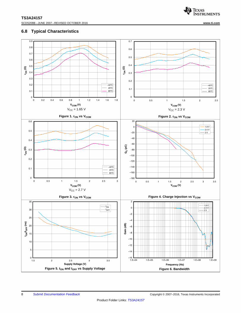
6.8 Typical Characteristics
VCC = 1.65 V
Figure 1. rON vs VCOM
VCC = 2.3 V
Figure 2. rON vs VCOM
VCC = 2.7 V
Figure 3. rON vs VCOM Figure 4. Charge Injection vs VCOM
Figure 5. tON and tOFF vs Supply Voltage Figure 6. Bandwidth
–5.E-08
0.E+00
5.E-08
1.E-07
2.E-07
2.E-07
3.E-07
3.E-07
4.E-07
4.E-07
0 0.5 1 1.5 2 2.5 3 3.5 4
V (V)+
I(A
)+
–40 Cº
25ºC
85ºC
–80
–70
–60
–50
–40
–30
–20
–10
0
1.E+03 1.E+04 1.E+05 1.E+06 1.E+07 1.E+08 1.E+09
Frequency (Hz)
Cro
ssta
lk (
dB
)
1.8 V
2.5 V
3 V
–9E+01
–8E+01
–7E+01
–6E+01
–5E+01
–4E+01
–3E+01
–2E+01
–1E+01
0E+00
1E+04 1E+05 1E+06 1E+07 1E+08 1E+09
Frequency (Hz)
Off
Iso
lati
on
(d
B)
1.8 V
2.5 V
3 V
9
TS3A24157www.ti.com SCDS208B –JUNE 2007–REVISED OCTOBER 2016
Product Folder Links: TS3A24157
Submit Documentation FeedbackCopyright © 2007–2016, Texas Instruments Incorporated
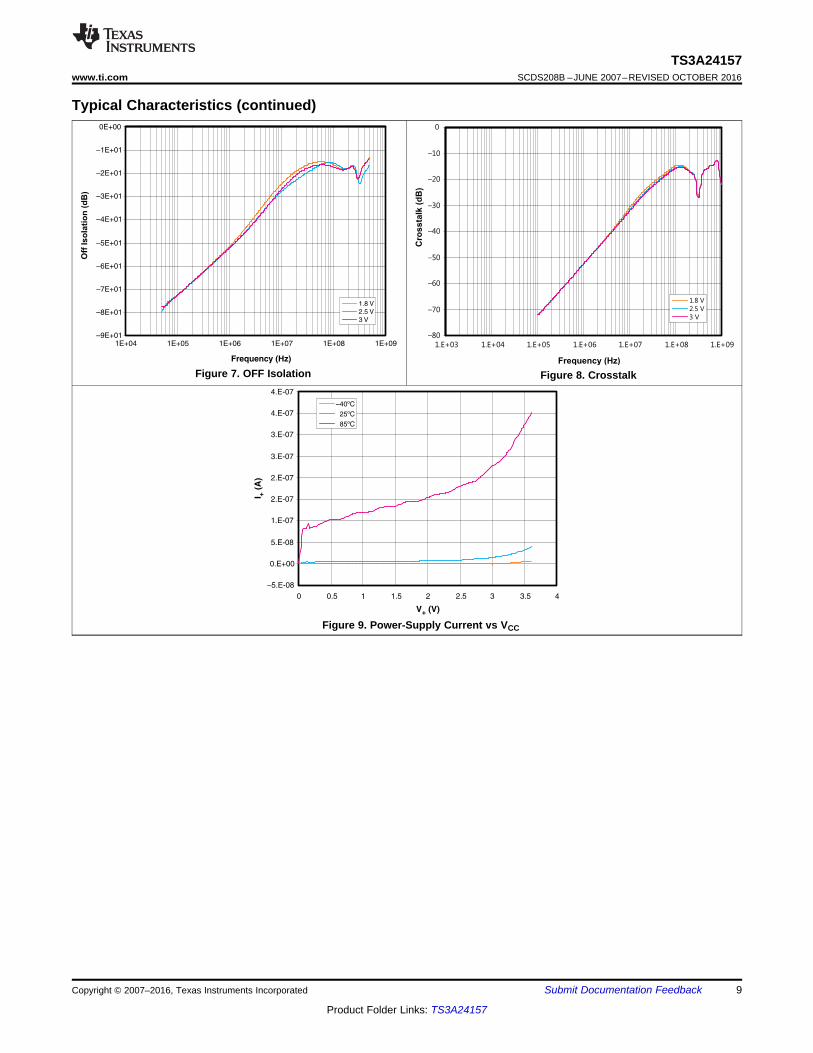
Typical Characteristics (continued)
Figure 7. OFF Isolation Figure 8. Crosstalk
Figure 9. Power-Supply Current vs VCC
Channel ON
ON-State Leakage Current
VI = VIH or V IL
VCC
GND
NC
VI
NO
COMVCOM
VNO
VNC
+
+
IN
Channel OFF
OFF-State Leakage Current
VI = VIH or V IL
VCC
GND
NC
VI
NO
COM VCOM
VNO
VNC
+
+
+
IN
VCC
ICOM
ron =
ICOM
GND
Channel ON
NC
VI
NO
COM VCOM
VI = VIH or V IL
VNO
VNC
+
+
IN
VCOM –VNO or VNC
10
TS3A24157SCDS208B –JUNE 2007–REVISED OCTOBER 2016 www.ti.com
Product Folder Links: TS3A24157
Submit Documentation Feedback Copyright © 2007–2016, Texas Instruments Incorporated
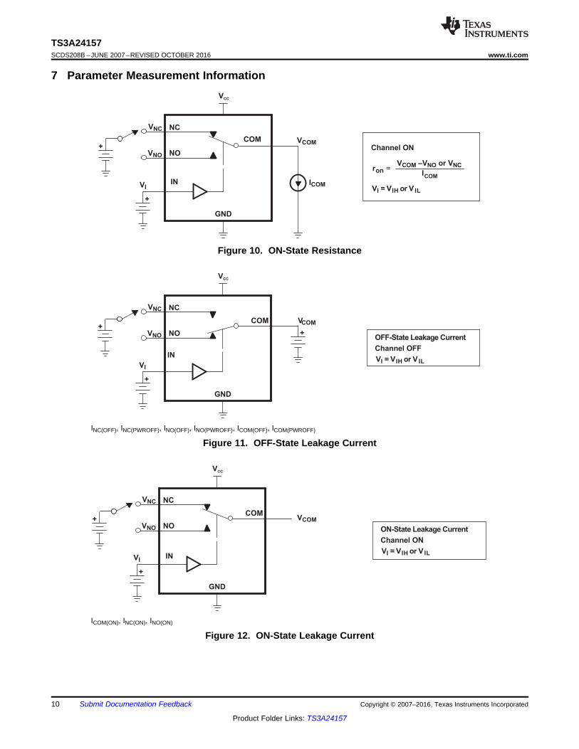
7 Parameter Measurement Information
Figure 10. ON-State Resistance
INC(OFF), INC(PWROFF), INO(OFF), INO(PWROFF), ICOM(OFF), ICOM(PWROFF)
Figure 11. OFF-State Leakage Current
ICOM(ON), INC(ON), INO(ON)
Figure 12. ON-State Leakage Current
CL(2) RL
VCOM
VCC
GND
NC or NO VNC or VNO
VI
NC or NO
COM
(1)
VCC
VCOM
50 Ω
RL CL
35 pFtON
TEST
VCC50 Ω 35 pFtOFF
50%
tON tOFF
50%
90% 90%
Logic
Input
(VI)
VCC
(VNC or VNO)
0
CL(2) RL
IN
VCC
GND
VBI AS
VI
VI = VCC or GND
VBI AS= VCC or GND
Capacitance is measured at NC,
NO, COM, and IN inputs during
ON and OFF conditions.
Capacitance
Meter
VCOM
VNO
VNC
COM
NO
NC
IN
11
TS3A24157www.ti.com SCDS208B –JUNE 2007–REVISED OCTOBER 2016
Product Folder Links: TS3A24157
Submit Documentation FeedbackCopyright © 2007–2016, Texas Instruments Incorporated
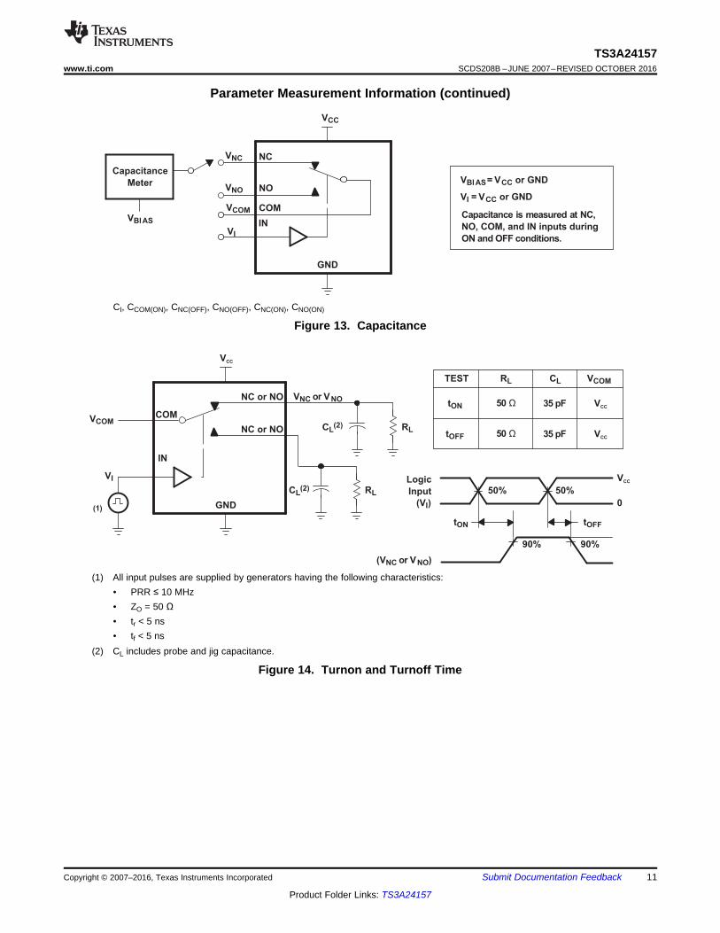
Parameter Measurement Information (continued)
CI, CCOM(ON), CNC(OFF), CNO(OFF), CNC(ON), CNO(ON)
Figure 13. Capacitance
(1) All input pulses are supplied by generators having the following characteristics:• PRR ≤ 10 MHz• ZO = 50 Ω• tr < 5 ns• tf < 5 ns
(2) CL includes probe and jig capacitance.
Figure 14. Turnon and Turnoff Time
NC
NO
COM
VNC
VCOM
Channel OFF: NC to COM
Network Analyzer Setup
Source Power = 0 dBm
(632-mV P-P at 50-Ωload)
50 Ω
VCC
GND
50 Ω
50 Ω
Network Analyzer
Source
Signal
VI
+
VI = VCC or GND
IN
DC Bias = 350 mV
VCC
GND
NC
VI
NO
COM
50 Ω
50 Ω
VNC
VCOM
Channel ON: NC to COM
Network Analyzer Setup
Source Power = 0 dBm
(632-mV P-P at 50-Ω load)
DC Bias = 350 mV
Network Analyzer
Source
Signal
+
VI = VCC or GND
IN
VCC
GND
NC or NO
VNC or VNO
VI
NC or NO
COM
VCOM
CL(2) RL
tBBM
50%
90% 90%
Logic
Input
(VI)
(VCOM)
V+
0
IN
VNC or VNO = VCC
RL = 50
CL = 35 pF
Logic
Input(1)
12
TS3A24157SCDS208B –JUNE 2007–REVISED OCTOBER 2016 www.ti.com
Product Folder Links: TS3A24157
Submit Documentation Feedback Copyright © 2007–2016, Texas Instruments Incorporated
Parameter Measurement Information (continued)
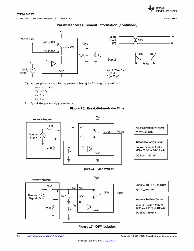
(1) All input pulses are supplied by generators having the following characteristics:• PRR ≤ 10 MHz• ZO = 50 Ω• tr < 5 ns• tf < 5 ns
A. CL includes probe and jig capacitance.
Figure 15. Break-Before-Make Time
Figure 16. Bandwidth
Figure 17. OFF Isolation
GND
NO
COM
10 µF
CL(1)
RL10 µF
INVI
600 Ω60 Ω0
60 Ω0
Audio Analyzer
Source
Signal
Source Signal = 20 Hz to 20 kHz
Channel ON: COM to NO VI = VIH or V IL RL = 600 Ω
CL = 50 pF
VCC /2
VCC
VSOURCE = VCCP-P
GND
NC or NO
IN
RGEN
VI
NC or NO
COM VCOM
CL(2)
OFF
VCOM
ON OFF
ΔVCOMVGEN
+
VI = VIH or V IL
CL = 1 nF
VGEN = 0 to VCC
RGEN = 0
QC = CL ×⋅ΔVCOM
VIH
VIL
Logic
Input
(VI)
Logic
Input(1)
VCC
NC
NO
50 Ω
50 Ω
VNC
VCOM
Channel ON: NC to COM
Network Analyzer Setup
Source Power = 0 dBm
(632-mV P-P at 50-Ω load)
50 Ω
GND
VNO
Source
Signal
Channel OFF: NO to COM
Network Analyzer
VI
+
VI = VCCor GND
IN
DC Bias = 350 mV
VCC
13
TS3A24157www.ti.com SCDS208B –JUNE 2007–REVISED OCTOBER 2016
Product Folder Links: TS3A24157
Submit Documentation FeedbackCopyright © 2007–2016, Texas Instruments Incorporated
Parameter Measurement Information (continued)
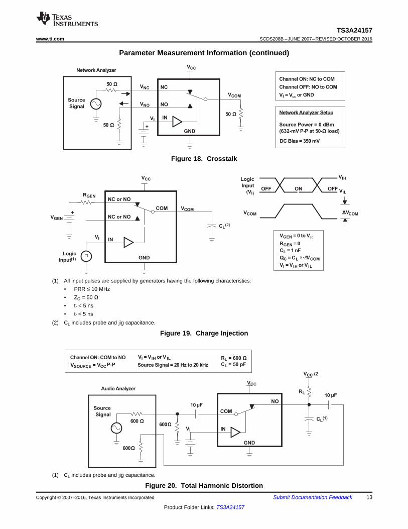
Figure 18. Crosstalk
(1) All input pulses are supplied by generators having the following characteristics:• PRR ≤ 10 MHz• ZO = 50 Ω• tr < 5 ns• tf < 5 ns
(2) CL includes probe and jig capacitance.
Figure 19. Charge Injection
(1) CL includes probe and jig capacitance.
Figure 20. Total Harmonic Distortion
IN1
COM1NC1
NO1
SPDT
Logic Control
IN2
COM2NC2
NO2
SPDT
Logic Control
Copyright © 2016, Texas Instruments Incorporated
14
TS3A24157SCDS208B –JUNE 2007–REVISED OCTOBER 2016 www.ti.com
Product Folder Links: TS3A24157
Submit Documentation Feedback Copyright © 2007–2016, Texas Instruments Incorporated
8 Detailed Description
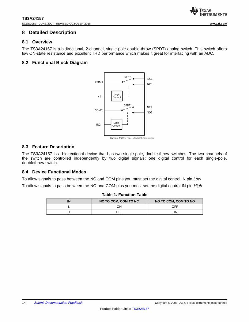
8.1 OverviewThe TS3A24157 is a bidirectional, 2-channel, single-pole double-throw (SPDT) analog switch. This switch offerslow ON-state resistance and excellent THD performance which makes it great for interfacing with an ADC.
8.2 Functional Block Diagram
8.3 Feature DescriptionThe TS3A24157 is a bidirectional device that has two single-pole, double-throw switches. The two channels ofthe switch are controlled independently by two digital signals; one digital control for each single-pole,doublethrow switch.
8.4 Device Functional ModesTo allow signals to pass between the NC and COM pins you must set the digital control IN pin Low
To allow signals to pass between the NO and COM pins you must set the digital control IN pin High
Table 1. Function TableIN NC TO COM, COM TO NC NO TO COM, COM TO NOL ON OFFH OFF ON
TS3A24157VCC
IN1IN2
COM1
COM4
GND
NO1
SystemController
Device 1
Device 2
0.1 mF0.1 mF
3.3 V
Signal Path
Switch Control Logic NC1
Device 3NO2
NC2 Device 4COM2
Copyright © 2016, Texas Instruments Incorporated
15
TS3A24157www.ti.com SCDS208B –JUNE 2007–REVISED OCTOBER 2016
Product Folder Links: TS3A24157
Submit Documentation FeedbackCopyright © 2007–2016, Texas Instruments Incorporated
9 Application and Implementation
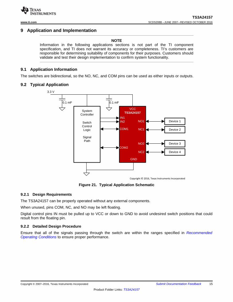
NOTEInformation in the following applications sections is not part of the TI componentspecification, and TI does not warrant its accuracy or completeness. TI’s customers areresponsible for determining suitability of components for their purposes. Customers shouldvalidate and test their design implementation to confirm system functionality.
9.1 Application InformationThe switches are bidirectional, so the NO, NC, and COM pins can be used as either inputs or outputs.
9.2 Typical Application
Figure 21. Typical Application Schematic
9.2.1 Design RequirementsThe TS3A24157 can be properly operated without any external components.
When unused, pins COM, NC, and NO may be left floating.
Digital control pins IN must be pulled up to VCC or down to GND to avoid undesired switch positions that couldresult from the floating pin.
9.2.2 Detailed Design ProcedureEnsure that all of the signals passing through the switch are within the ranges specified in RecommendedOperating Conditions to ensure proper performance.
0603 Cap
VC
C
= VIA to GND Plane
To Device 2
To Device 3NC2
To Device 3NO1
NC1
To Device 3NO2
To Device 3GND
To Device 3
To Device 4
To Device 1/2
To Device 3IN1
To Device 3COM1
To Device 3IN2
To Device 3COM2
To System
To System
To Device 3VCC
To Device 3/4
To Device 1
0
0.1
0.2
0.3
0.4
0.5
0.6
0 0.5 1 1.5 2 2.5 3
r(
)O
NΩ
–40 Cº
25ºC
85ºC
V (V)COM
16
TS3A24157SCDS208B –JUNE 2007–REVISED OCTOBER 2016 www.ti.com
Product Folder Links: TS3A24157
Submit Documentation Feedback Copyright © 2007–2016, Texas Instruments Incorporated
Typical Application (continued)9.2.3 Application Curves
VCC = 2.7 VFigure 22. rON vs VCOM
10 Power Supply RecommendationsTI recommends proper power-supply sequencing for all CMOS devices. Do not exceed the absolute-maximumratings, because stresses beyond the listed ratings can cause permanent damage to the device. Alwayssequence VCC on first, followed by NO, NC, or COM. Although it is not required, power-supply bypassingimproves noise margin and prevents switching noise propagation from the VCC supply to other components. A0.1-μF capacitor, connected from VCC to GND, is adequate for most applications
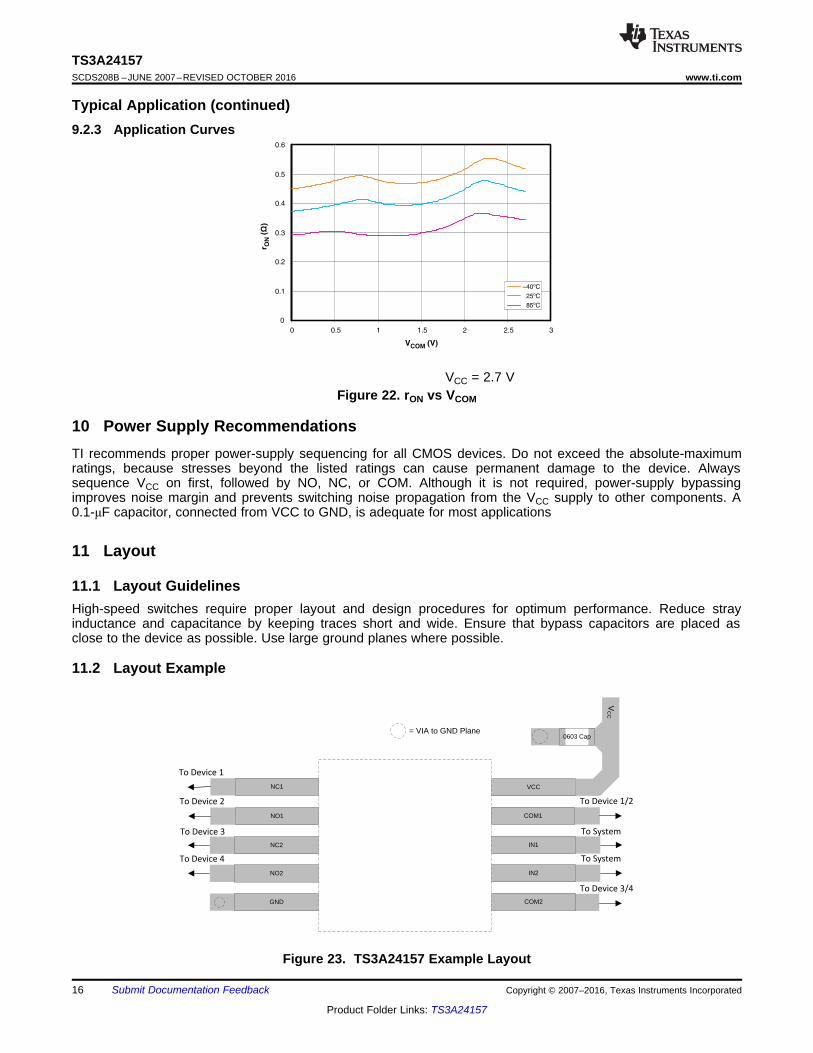
11 Layout
11.1 Layout GuidelinesHigh-speed switches require proper layout and design procedures for optimum performance. Reduce strayinductance and capacitance by keeping traces short and wide. Ensure that bypass capacitors are placed asclose to the device as possible. Use large ground planes where possible.
11.2 Layout Example
Figure 23. TS3A24157 Example Layout
17
TS3A24157www.ti.com SCDS208B –JUNE 2007–REVISED OCTOBER 2016
Product Folder Links: TS3A24157
Submit Documentation FeedbackCopyright © 2007–2016, Texas Instruments Incorporated
12 Device and Documentation Support
12.1 Device Support
12.1.1 Device NomenclatureVCOM Voltage at COM.
VNC Voltage at NC.
VNO Voltage at NO.
rON Resistance between COM and NC or COM and NO ports when the channel is ON.
rPEAK Peak ON-state resistance over a specified voltage range.
ΔrON Difference of rON between channels in a specific device.
rON(FLAT) Difference between the maximum and minimum value of rON in a channel over the specified rangeof conditions.
INC(OFF) Leakage current measured at the NC port, with the corresponding channel (NC to COM) in the OFFstate under worst-case input and output conditions.
INC(PWROFF) Leakage current measured at the NC port during the power-down condition (VCC = 0).
INO(OFF) Leakage current measured at the NO port, with the corresponding channel (NO to COM) in theOFF state under worst-case input and output conditions.
INO(PWROFF) Leakage current measured at the NO port during the power-down condition (VCC = 0).
INC(ON) Leakage current measured at the NC port, with the corresponding channel (NC to COM) in the ONstate and the output (COM) open.
INO(ON) Leakage current measured at the NO port, with the corresponding channel (NO to COM) in the ONstate and the output (COM) open.
ICOM(ON) Leakage current measured at the COM port, with the corresponding channel (COM to NO or COMto NC) in the ON state and the output (NC or NO) open.
ICOM(PWROFF) Leakage current measured at the COM port during the power-down condition (VCC = 0).
VIH Minimum input voltage for logic high for the control input (IN).
VIL Maximum input voltage for logic low for the control input (IN).
VI Voltage at the control input (IN).
IIH, IIL Leakage current measured at the control input (IN).
tON Turnon time for the switch. This parameter is measured under the specified range of conditions andby the propagation delay between the digital control (IN) signal and analog output (COM, NC, orNO) signal when the switch is turning ON.
tOFF Turnoff time for the switch. This parameter is measured under the specified range of conditions andby the propagation delay between the digital control (IN) signal and analog output (COM, NC, orNO) signal when the switch is turning OFF.
tBBM Break-before-make time. This parameter is measured under the specified range of conditions andby the propagation delay between the output of two adjacent analog channels (NC and NO) whenthe control signal changes state.
QC Charge injection is a measurement of unwanted signal coupling from the control (IN) input to theanalog (NC, NO, or COM) output. This is measured in coulomb (C) and measured by the totalcharge induced due to switching of the control input. Charge injection, QC = CL × ΔVCOM, CL is theload capacitance and ΔVCOM is the change in analog output voltage.
CNC(OFF) Capacitance at the NC port when the corresponding channel (NC to COM) is OFF.
CNO(OFF) Capacitance at the NO port when the corresponding channel (NO to COM) is OFF.
18
TS3A24157SCDS208B –JUNE 2007–REVISED OCTOBER 2016 www.ti.com
Product Folder Links: TS3A24157
Submit Documentation Feedback Copyright © 2007–2016, Texas Instruments Incorporated
Device Support (continued)CNC(ON) Capacitance at the NC port when the corresponding channel (NC to COM) is ON.
CNO(ON) Capacitance at the NO port when the corresponding channel (NO to COM) is ON.
CCOM(ON) Capacitance at the COM port when the corresponding channel (COM to NC or COM to NO) is ON.
CI Capacitance of control input (IN).
OISO OFF isolation of the switch is a measurement of OFF-state switch impedance. This is measured indB in a specific frequency, with the corresponding channel (NC to COM or NO to COM) in the OFFstate.
XTALK Crosstalk is a measurement of unwanted signal coupling from an ON channel to an OFF channel(NC to NO or NO to NC). This is measured in a specific frequency and in dB.
BW Bandwidth of the switch. This is the frequency in which the gain of an ON channel is –3 dB belowthe DC gain.
THD Total harmonic distortion describes the signal distortion caused by the analog switch. This isdefined as the ratio of root mean square (RMS) value of the second, third, and higher harmonic tothe absolute magnitude of the fundamental harmonic.
ICC Static power-supply current with the control (IN) pin at VCC or GND.
12.2 Documentation Support
12.2.1 Related DocumentationFor related documentation see the following:
Implications of Slow or Floating CMOS Inputs (SCBA004)
12.3 Receiving Notification of Documentation UpdatesTo receive notification of documentation updates, navigate to the device product folder on ti.com. In the upperright corner, click on Alert me to register and receive a weekly digest of any product information that haschanged. For change details, review the revision history included in any revised document.
12.4 Community ResourcesThe following links connect to TI community resources. Linked contents are provided "AS IS" by the respectivecontributors. They do not constitute TI specifications and do not necessarily reflect TI's views; see TI's Terms ofUse.
TI E2E™ Online Community TI's Engineer-to-Engineer (E2E) Community. Created to foster collaborationamong engineers. At e2e.ti.com, you can ask questions, share knowledge, explore ideas and helpsolve problems with fellow engineers.
Design Support TI's Design Support Quickly find helpful E2E forums along with design support tools andcontact information for technical support.
12.5 TrademarksE2E is a trademark of Texas Instruments.All other trademarks are the property of their respective owners.
12.6 Electrostatic Discharge CautionThese devices have limited built-in ESD protection. The leads should be shorted together or the device placed in conductive foamduring storage or handling to prevent electrostatic damage to the MOS gates.
12.7 GlossarySLYZ022 — TI Glossary.
This glossary lists and explains terms, acronyms, and definitions.
19
TS3A24157www.ti.com SCDS208B –JUNE 2007–REVISED OCTOBER 2016
Product Folder Links: TS3A24157
Submit Documentation FeedbackCopyright © 2007–2016, Texas Instruments Incorporated
13 Mechanical, Packaging, and Orderable InformationThe following pages include mechanical, packaging, and orderable information. This information is the mostcurrent data available for the designated devices. This data is subject to change without notice and revision ofthis document. For browser-based versions of this data sheet, refer to the left-hand navigation.
PACKAGE OPTION ADDENDUM
www.ti.com 15-Apr-2017
Addendum-Page 1
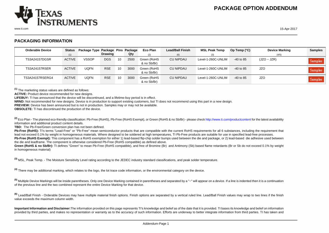
PACKAGING INFORMATION
Orderable Device Status(1)
Package Type PackageDrawing
Pins PackageQty
Eco Plan(2)
Lead/Ball Finish(6)
MSL Peak Temp(3)
Op Temp (°C) Device Marking(4/5)
Samples
TS3A24157DGSR ACTIVE VSSOP DGS 10 2500 Green (RoHS& no Sb/Br)
CU NIPDAU Level-1-260C-UNLIM -40 to 85 (JZO ~ JZR)
TS3A24157RSER ACTIVE UQFN RSE 10 3000 Green (RoHS& no Sb/Br)
CU NIPDAU Level-1-260C-UNLIM -40 to 85 JZO
TS3A24157RSERG4 ACTIVE UQFN RSE 10 3000 Green (RoHS& no Sb/Br)
CU NIPDAU Level-1-260C-UNLIM -40 to 85 JZO
(1) The marketing status values are defined as follows:ACTIVE: Product device recommended for new designs.LIFEBUY: TI has announced that the device will be discontinued, and a lifetime-buy period is in effect.NRND: Not recommended for new designs. Device is in production to support existing customers, but TI does not recommend using this part in a new design.PREVIEW: Device has been announced but is not in production. Samples may or may not be available.OBSOLETE: TI has discontinued the production of the device.
(2) Eco Plan - The planned eco-friendly classification: Pb-Free (RoHS), Pb-Free (RoHS Exempt), or Green (RoHS & no Sb/Br) - please check http://www.ti.com/productcontent for the latest availabilityinformation and additional product content details.TBD: The Pb-Free/Green conversion plan has not been defined.Pb-Free (RoHS): TI's terms "Lead-Free" or "Pb-Free" mean semiconductor products that are compatible with the current RoHS requirements for all 6 substances, including the requirement thatlead not exceed 0.1% by weight in homogeneous materials. Where designed to be soldered at high temperatures, TI Pb-Free products are suitable for use in specified lead-free processes.Pb-Free (RoHS Exempt): This component has a RoHS exemption for either 1) lead-based flip-chip solder bumps used between the die and package, or 2) lead-based die adhesive used betweenthe die and leadframe. The component is otherwise considered Pb-Free (RoHS compatible) as defined above.Green (RoHS & no Sb/Br): TI defines "Green" to mean Pb-Free (RoHS compatible), and free of Bromine (Br) and Antimony (Sb) based flame retardants (Br or Sb do not exceed 0.1% by weightin homogeneous material)
(3) MSL, Peak Temp. - The Moisture Sensitivity Level rating according to the JEDEC industry standard classifications, and peak solder temperature.
(4) There may be additional marking, which relates to the logo, the lot trace code information, or the environmental category on the device.
(5) Multiple Device Markings will be inside parentheses. Only one Device Marking contained in parentheses and separated by a "~" will appear on a device. If a line is indented then it is a continuationof the previous line and the two combined represent the entire Device Marking for that device.
(6) Lead/Ball Finish - Orderable Devices may have multiple material finish options. Finish options are separated by a vertical ruled line. Lead/Ball Finish values may wrap to two lines if the finishvalue exceeds the maximum column width.
Important Information and Disclaimer:The information provided on this page represents TI's knowledge and belief as of the date that it is provided. TI bases its knowledge and belief on informationprovided by third parties, and makes no representation or warranty as to the accuracy of such information. Efforts are underway to better integrate information from third parties. TI has taken and
PACKAGE OPTION ADDENDUM
www.ti.com 15-Apr-2017
Addendum-Page 2
continues to take reasonable steps to provide representative and accurate information but may not have conducted destructive testing or chemical analysis on incoming materials and chemicals.TI and TI suppliers consider certain information to be proprietary, and thus CAS numbers and other limited information may not be available for release.
In no event shall TI's liability arising out of such information exceed the total purchase price of the TI part(s) at issue in this document sold by TI to Customer on an annual basis.
TAPE AND REEL INFORMATION
*All dimensions are nominal
Device PackageType
PackageDrawing
Pins SPQ ReelDiameter
(mm)
ReelWidth
W1 (mm)
A0(mm)
B0(mm)
K0(mm)
P1(mm)
W(mm)
Pin1Quadrant
TS3A24157DGSR VSSOP DGS 10 2500 330.0 12.4 5.3 3.3 1.3 8.0 12.0 Q1
TS3A24157RSER UQFN RSE 10 3000 179.0 8.4 1.75 2.25 0.65 4.0 8.0 Q1
PACKAGE MATERIALS INFORMATION
www.ti.com 3-Aug-2017
Pack Materials-Page 1
*All dimensions are nominal
Device Package Type Package Drawing Pins SPQ Length (mm) Width (mm) Height (mm)
TS3A24157DGSR VSSOP DGS 10 2500 346.0 346.0 35.0
TS3A24157RSER UQFN RSE 10 3000 203.0 203.0 35.0
PACKAGE MATERIALS INFORMATION
www.ti.com 3-Aug-2017
Pack Materials-Page 2
IMPORTANT NOTICE
Texas Instruments Incorporated (TI) reserves the right to make corrections, enhancements, improvements and other changes to itssemiconductor products and services per JESD46, latest issue, and to discontinue any product or service per JESD48, latest issue. Buyersshould obtain the latest relevant information before placing orders and should verify that such information is current and complete.TI’s published terms of sale for semiconductor products (http://www.ti.com/sc/docs/stdterms.htm) apply to the sale of packaged integratedcircuit products that TI has qualified and released to market. Additional terms may apply to the use or sale of other types of TI products andservices.Reproduction of significant portions of TI information in TI data sheets is permissible only if reproduction is without alteration and isaccompanied by all associated warranties, conditions, limitations, and notices. TI is not responsible or liable for such reproduceddocumentation. Information of third parties may be subject to additional restrictions. Resale of TI products or services with statementsdifferent from or beyond the parameters stated by TI for that product or service voids all express and any implied warranties for theassociated TI product or service and is an unfair and deceptive business practice. TI is not responsible or liable for any such statements.Buyers and others who are developing systems that incorporate TI products (collectively, “Designers”) understand and agree that Designersremain responsible for using their independent analysis, evaluation and judgment in designing their applications and that Designers havefull and exclusive responsibility to assure the safety of Designers' applications and compliance of their applications (and of all TI productsused in or for Designers’ applications) with all applicable regulations, laws and other applicable requirements. Designer represents that, withrespect to their applications, Designer has all the necessary expertise to create and implement safeguards that (1) anticipate dangerousconsequences of failures, (2) monitor failures and their consequences, and (3) lessen the likelihood of failures that might cause harm andtake appropriate actions. Designer agrees that prior to using or distributing any applications that include TI products, Designer willthoroughly test such applications and the functionality of such TI products as used in such applications.TI’s provision of technical, application or other design advice, quality characterization, reliability data or other services or information,including, but not limited to, reference designs and materials relating to evaluation modules, (collectively, “TI Resources”) are intended toassist designers who are developing applications that incorporate TI products; by downloading, accessing or using TI Resources in anyway, Designer (individually or, if Designer is acting on behalf of a company, Designer’s company) agrees to use any particular TI Resourcesolely for this purpose and subject to the terms of this Notice.TI’s provision of TI Resources does not expand or otherwise alter TI’s applicable published warranties or warranty disclaimers for TIproducts, and no additional obligations or liabilities arise from TI providing such TI Resources. TI reserves the right to make corrections,enhancements, improvements and other changes to its TI Resources. TI has not conducted any testing other than that specificallydescribed in the published documentation for a particular TI Resource.Designer is authorized to use, copy and modify any individual TI Resource only in connection with the development of applications thatinclude the TI product(s) identified in such TI Resource. NO OTHER LICENSE, EXPRESS OR IMPLIED, BY ESTOPPEL OR OTHERWISETO ANY OTHER TI INTELLECTUAL PROPERTY RIGHT, AND NO LICENSE TO ANY TECHNOLOGY OR INTELLECTUAL PROPERTYRIGHT OF TI OR ANY THIRD PARTY IS GRANTED HEREIN, including but not limited to any patent right, copyright, mask work right, orother intellectual property right relating to any combination, machine, or process in which TI products or services are used. Informationregarding or referencing third-party products or services does not constitute a license to use such products or services, or a warranty orendorsement thereof. Use of TI Resources may require a license from a third party under the patents or other intellectual property of thethird party, or a license from TI under the patents or other intellectual property of TI.TI RESOURCES ARE PROVIDED “AS IS” AND WITH ALL FAULTS. TI DISCLAIMS ALL OTHER WARRANTIES ORREPRESENTATIONS, EXPRESS OR IMPLIED, REGARDING RESOURCES OR USE THEREOF, INCLUDING BUT NOT LIMITED TOACCURACY OR COMPLETENESS, TITLE, ANY EPIDEMIC FAILURE WARRANTY AND ANY IMPLIED WARRANTIES OFMERCHANTABILITY, FITNESS FOR A PARTICULAR PURPOSE, AND NON-INFRINGEMENT OF ANY THIRD PARTY INTELLECTUALPROPERTY RIGHTS. TI SHALL NOT BE LIABLE FOR AND SHALL NOT DEFEND OR INDEMNIFY DESIGNER AGAINST ANY CLAIM,INCLUDING BUT NOT LIMITED TO ANY INFRINGEMENT CLAIM THAT RELATES TO OR IS BASED ON ANY COMBINATION OFPRODUCTS EVEN IF DESCRIBED IN TI RESOURCES OR OTHERWISE. IN NO EVENT SHALL TI BE LIABLE FOR ANY ACTUAL,DIRECT, SPECIAL, COLLATERAL, INDIRECT, PUNITIVE, INCIDENTAL, CONSEQUENTIAL OR EXEMPLARY DAMAGES INCONNECTION WITH OR ARISING OUT OF TI RESOURCES OR USE THEREOF, AND REGARDLESS OF WHETHER TI HAS BEENADVISED OF THE POSSIBILITY OF SUCH DAMAGES.Unless TI has explicitly designated an individual product as meeting the requirements of a particular industry standard (e.g., ISO/TS 16949and ISO 26262), TI is not responsible for any failure to meet such industry standard requirements.Where TI specifically promotes products as facilitating functional safety or as compliant with industry functional safety standards, suchproducts are intended to help enable customers to design and create their own applications that meet applicable functional safety standardsand requirements. Using products in an application does not by itself establish any safety features in the application. Designers mustensure compliance with safety-related requirements and standards applicable to their applications. Designer may not use any TI products inlife-critical medical equipment unless authorized officers of the parties have executed a special contract specifically governing such use.Life-critical medical equipment is medical equipment where failure of such equipment would cause serious bodily injury or death (e.g., lifesupport, pacemakers, defibrillators, heart pumps, neurostimulators, and implantables). Such equipment includes, without limitation, allmedical devices identified by the U.S. Food and Drug Administration as Class III devices and equivalent classifications outside the U.S.TI may expressly designate certain products as completing a particular qualification (e.g., Q100, Military Grade, or Enhanced Product).Designers agree that it has the necessary expertise to select the product with the appropriate qualification designation for their applicationsand that proper product selection is at Designers’ own risk. Designers are solely responsible for compliance with all legal and regulatoryrequirements in connection with such selection.Designer will fully indemnify TI and its representatives against any damages, costs, losses, and/or liabilities arising out of Designer’s non-compliance with the terms and provisions of this Notice.
Mailing Address: Texas Instruments, Post Office Box 655303, Dallas, Texas 75265Copyright © 2017, Texas Instruments Incorporated