
TPS767xxQ Fast-Transient-Response 1-A Low-Dropout · PDF filethe end of the datasheet....
32
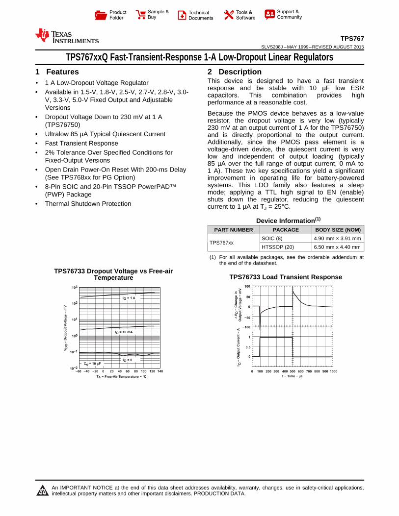
T A - Free-Air Temperature - °C -40 0 20 120 10 3 -60 40 60 80 100 - Dropout Voltage - mV V DO 10 2 10 1 10 0 10 -1 10 -2 -20 140 I O = 1 A I O = 10 mA I O = 0 C o = 10 μF t - Time - μs I - Output Current - A O V O - Change in Δ Output Voltage - mV 1 0.5 300 200 100 400 500 700 600 800 900 1000 0 0 0 50 100 -50 Product Folder Sample & Buy Technical Documents Tools & Software Support & Community TPS767 SLVS208J – MAY 1999 – REVISED AUGUST 2015 TPS767xxQ Fast-Transient-Response 1-A Low-Dropout Linear Regulators 1 Features 2 Description This device is designed to have a fast transient 1• 1 A Low-Dropout Voltage Regulator response and be stable with 10 μF low ESR • Available in 1.5-V, 1.8-V, 2.5-V, 2.7-V, 2.8-V, 3.0- capacitors. This combination provides high V, 3.3-V, 5.0-V Fixed Output and Adjustable performance at a reasonable cost. Versions Because the PMOS device behaves as a low-value • Dropout Voltage Down to 230 mV at 1 A resistor, the dropout voltage is very low (typically (TPS76750) 230 mV at an output current of 1 A for the TPS76750) • Ultralow 85 μA Typical Quiescent Current and is directly proportional to the output current. Additionally, since the PMOS pass element is a • Fast Transient Response voltage-driven device, the quiescent current is very • 2% Tolerance Over Specified Conditions for low and independent of output loading (typically Fixed-Output Versions 85 μA over the full range of output current, 0 mA to • Open Drain Power-On Reset With 200-ms Delay 1 A). These two key specifications yield a significant (See TPS768xx for PG Option) improvement in operating life for battery-powered systems. This LDO family also features a sleep • 8-Pin SOIC and 20-Pin TSSOP PowerPAD™ mode; applying a TTL high signal to EN (enable) (PWP) Package shuts down the regulator, reducing the quiescent • Thermal Shutdown Protection current to 1 μA at T J = 25°C. Device Information (1) PART NUMBER PACKAGE BODY SIZE (NOM) SOIC (8) 4.90 mm × 3.91 mm TPS767xx HTSSOP (20) 6.50 mm x 4.40 mm (1) For all available packages, see the orderable addendum at the end of the datasheet. TPS76733 Dropout Voltage vs Free-air TPS76733 Load Transient Response Temperature 1 An IMPORTANT NOTICE at the end of this data sheet addresses availability, warranty, changes, use in safety-critical applications, intellectual property matters and other important disclaimers. PRODUCTION DATA.
-
Upload
vuongkhanh -
Category
Documents
-
view
227 -
download
2
Transcript of TPS767xxQ Fast-Transient-Response 1-A Low-Dropout · PDF filethe end of the datasheet....
TA − Free-Air Temperature − °C
−40 0 20 120
103
−60 40 60 80 100
−D
rop
ou
tV
olt
ag
e−
mV
VD
O
102
101
100
10−1
10−2−20 140
IO = 1 A
IO = 10 mA
IO = 0Co = 10 μF
t − Time − μs
I−
Ou
tpu
t C
urr
en
t−
AO
VO
−C
han
ge in
∆
Ou
tpu
tV
olt
ag
e−
mV
1
0.5
300200100 400 500 700600 800 900 10000
0
0
50
100
−50
Product
Folder
Sample &Buy
Technical
Documents
Tools &
Software
Support &Community
TPS767SLVS208J –MAY 1999–REVISED AUGUST 2015
TPS767xxQ Fast-Transient-Response 1-A Low-Dropout Linear Regulators1 Features 2 Description
This device is designed to have a fast transient1• 1 A Low-Dropout Voltage Regulator
response and be stable with 10 µF low ESR• Available in 1.5-V, 1.8-V, 2.5-V, 2.7-V, 2.8-V, 3.0- capacitors. This combination provides highV, 3.3-V, 5.0-V Fixed Output and Adjustable performance at a reasonable cost.Versions
Because the PMOS device behaves as a low-value• Dropout Voltage Down to 230 mV at 1 A resistor, the dropout voltage is very low (typically(TPS76750) 230 mV at an output current of 1 A for the TPS76750)• Ultralow 85 µA Typical Quiescent Current and is directly proportional to the output current.
Additionally, since the PMOS pass element is a• Fast Transient Responsevoltage-driven device, the quiescent current is very• 2% Tolerance Over Specified Conditions for low and independent of output loading (typicallyFixed-Output Versions 85 µA over the full range of output current, 0 mA to
• Open Drain Power-On Reset With 200-ms Delay 1 A). These two key specifications yield a significant(See TPS768xx for PG Option) improvement in operating life for battery-powered
systems. This LDO family also features a sleep• 8-Pin SOIC and 20-Pin TSSOP PowerPAD™mode; applying a TTL high signal to EN (enable)(PWP) Packageshuts down the regulator, reducing the quiescent
• Thermal Shutdown Protection current to 1 µA at TJ = 25°C.
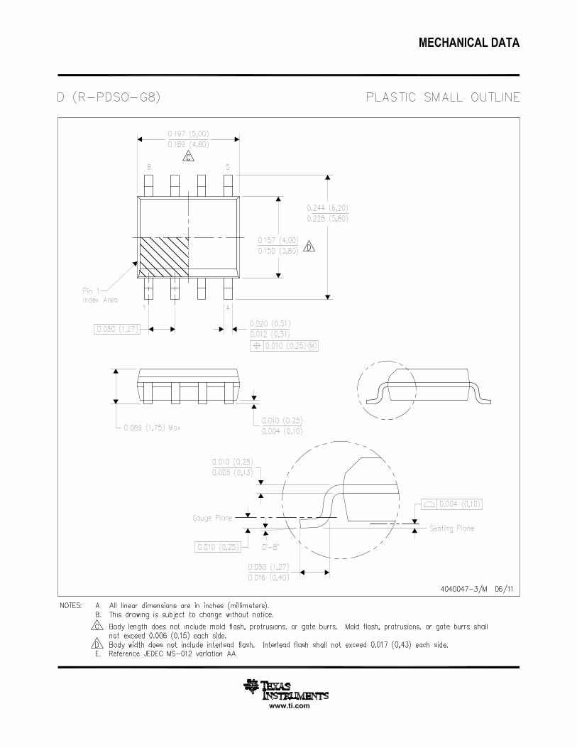
Device Information(1)
PART NUMBER PACKAGE BODY SIZE (NOM)SOIC (8) 4.90 mm × 3.91 mm
TPS767xxHTSSOP (20) 6.50 mm x 4.40 mm
(1) For all available packages, see the orderable addendum atthe end of the datasheet.
TPS76733 Dropout Voltage vs Free-airTPS76733 Load Transient ResponseTemperature
1
An IMPORTANT NOTICE at the end of this data sheet addresses availability, warranty, changes, use in safety-critical applications,intellectual property matters and other important disclaimers. PRODUCTION DATA.
TPS767SLVS208J –MAY 1999–REVISED AUGUST 2015 www.ti.com
Table of Contents9.2 Functional Block Diagram ....................................... 131 Features .................................................................. 19.3 Feature Description................................................. 142 Description ............................................................. 19.4 Device Functional Modes........................................ 153 Revision History..................................................... 29.5 Programming .......................................................... 154 Description (Continued) ........................................ 3
10 Application and Implementation........................ 165 Device Options....................................................... 310.1 Application Information.......................................... 166 Pin Configuration and Functions ......................... 410.2 Typical Application ............................................... 167 Specifications......................................................... 5 11 Layout................................................................... 187.1 Absolute Maximum Ratings ...................................... 511.1 Power Dissipation and Junction Temperature ...... 187.2 ESD Ratings.............................................................. 5
12 Device and Documentation Support ................. 197.3 Recommended Operating Conditions....................... 512.1 Related Links ........................................................ 197.4 Thermal Information .................................................. 512.2 Community Resources.......................................... 197.5 Electrical Characteristics........................................... 612.3 Trademarks ........................................................... 197.6 Typical Characteristics .............................................. 812.4 Electrostatic Discharge Caution............................ 198 Parameter Measurement Information ................ 1212.5 Glossary ................................................................ 199 Detailed Description ............................................ 13 13 Mechanical, Packaging, and Orderable9.1 Overview ................................................................. 13 Information ........................................................... 19
3 Revision History
Changes from Revision I (January 2004) to Revision J Page
• Added ESD Ratings table, Overview section, Feature Description section, Device Functional Modes, Applicationand Implementation section, Device and Documentation Support section, and Mechanical, Packaging, andOrderable Information section. .............................................................................................................................................. 1
2 Submit Documentation Feedback Copyright © 1999–2015, Texas Instruments Incorporated
TPS767www.ti.com SLVS208J –MAY 1999–REVISED AUGUST 2015
4 Description (Continued)The RESET output of the TPS767xx initiates a reset in microcomputer and microprocessor systems in the eventof an undervoltage condition. An internal comparator in the TPS767xx monitors the output voltage of theregulator to detect an undervoltage condition on the regulated output voltage.
The TPS767xx is offered in 1.5-V, 1.8-V, 2.5-V, 2.7-V, 2.8-V, 3.0-V, 3.3-V, and 5.0-V fixed-voltage versions andin an adjustable version (programmable over the range of 1.5 V to 5.5 V). Output voltage tolerance is specifiedas a maximum of 2% over line, load, and temperature ranges. The TPS767xx family is available in 8-pin SOICand 20-pin PWP packages.
5 Device Options
VOLTAGE OPTIONSPART NO. (1)(V)
TSSOP SOIC TYP(PWP) (D)TPS76750Q TPS76750Q 5TPS76733Q TPS76733Q 3.3TPS76730Q TPS76730Q 3TPS76728Q TPS76728Q 2.8TPS76727Q TPS76727Q 2.7TPS76725Q TPS76725Q 2.5TPS76718Q TPS76718Q 1.8TPS76715Q TPS76715Q 1.5TPS76701Q TPS76701Q Adjustable 1.5 V to 5.5 V
(1) The TPS76701 is programmable using an external resistor divider (see application information). The D and PWP packages are availabletaped and reeled. Add an R suffix to the device type (e.g., TPS76701QDR).
Copyright © 1999–2015, Texas Instruments Incorporated Submit Documentation Feedback 3
1
2
3
4
8
7
6
5
GND
EN
IN
IN
RESET
FB/NC
OUT
OUT
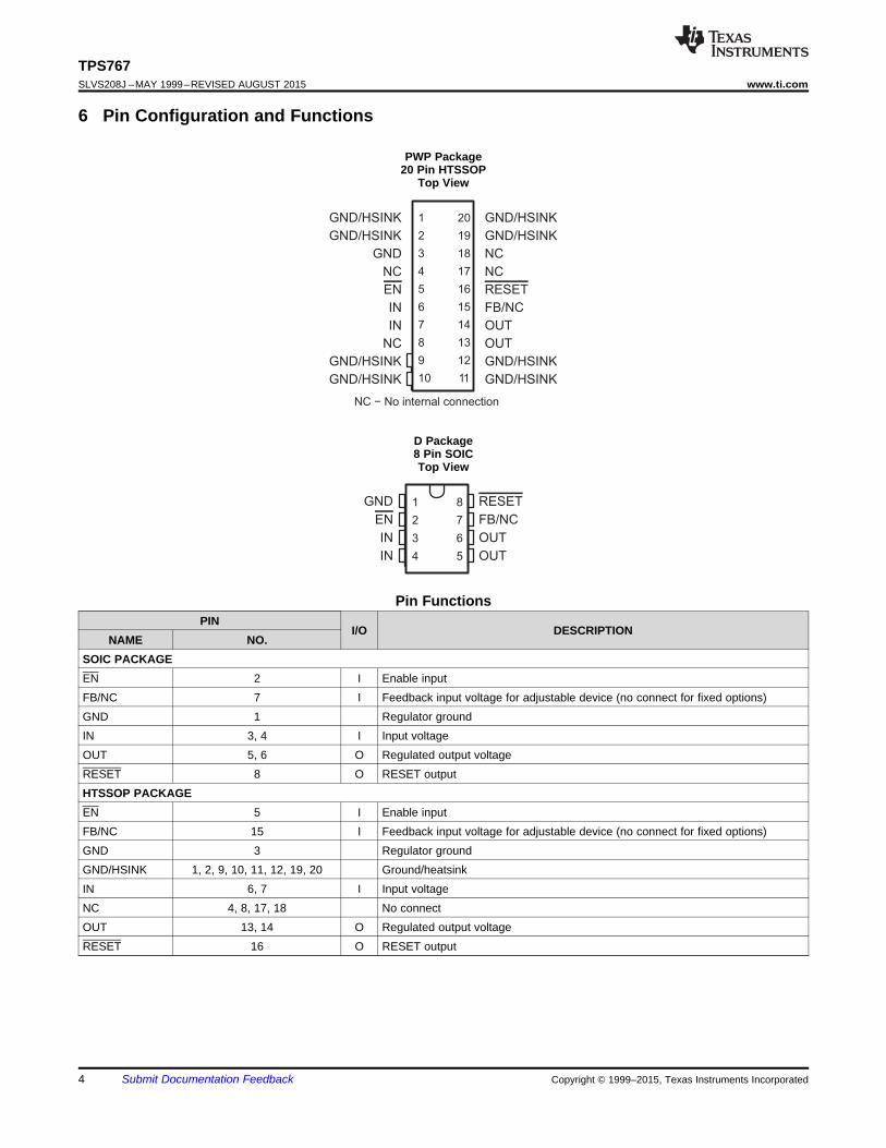
NC − No internal connection
1
2
3
4
5
6
7
8
9
10
20
19
18
17
16
15
14
13
12
11
GND/HSINK
GND/HSINK
GND
NC
EN
IN
IN
NC
GND/HSINK
GND/HSINK
GND/HSINK
GND/HSINK
NC
NC
RESET
FB/NC
OUT
OUT
GND/HSINK
GND/HSINK
TPS767SLVS208J –MAY 1999–REVISED AUGUST 2015 www.ti.com
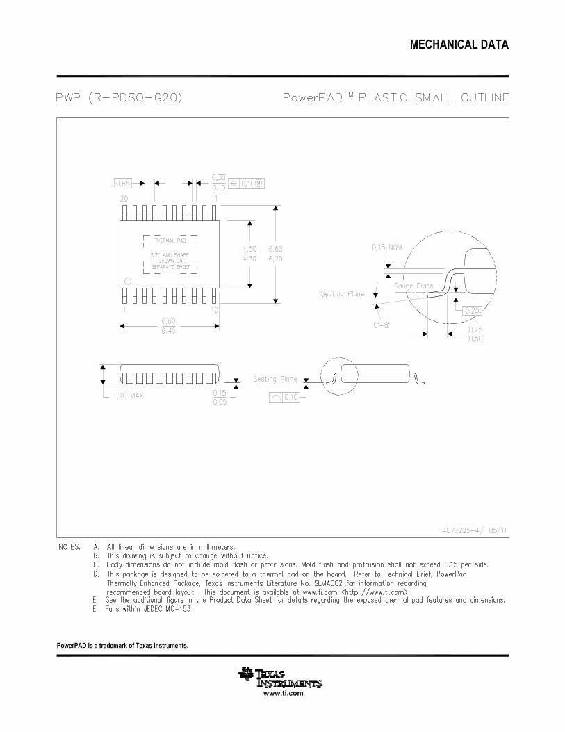
6 Pin Configuration and Functions
PWP Package20 Pin HTSSOP
Top View
D Package8 Pin SOICTop View
Pin FunctionsPIN
I/O DESCRIPTIONNAME NO.
SOIC PACKAGEEN 2 I Enable inputFB/NC 7 I Feedback input voltage for adjustable device (no connect for fixed options)GND 1 Regulator groundIN 3, 4 I Input voltageOUT 5, 6 O Regulated output voltageRESET 8 O RESET outputHTSSOP PACKAGEEN 5 I Enable inputFB/NC 15 I Feedback input voltage for adjustable device (no connect for fixed options)GND 3 Regulator groundGND/HSINK 1, 2, 9, 10, 11, 12, 19, 20 Ground/heatsinkIN 6, 7 I Input voltageNC 4, 8, 17, 18 No connectOUT 13, 14 O Regulated output voltageRESET 16 O RESET output
4 Submit Documentation Feedback Copyright © 1999–2015, Texas Instruments Incorporated
TPS767www.ti.com SLVS208J –MAY 1999–REVISED AUGUST 2015
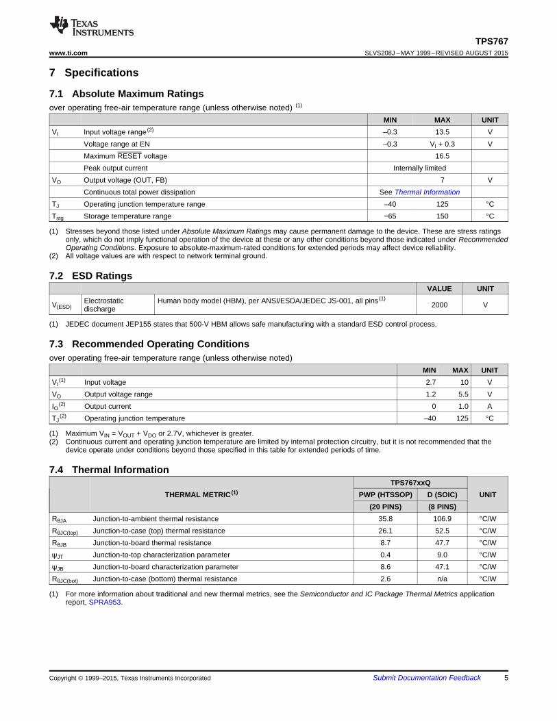
7 Specifications
7.1 Absolute Maximum Ratingsover operating free-air temperature range (unless otherwise noted) (1)
MIN MAX UNITVI Input voltage range (2) –0.3 13.5 V
Voltage range at EN –0.3 VI + 0.3 VMaximum RESET voltage 16.5Peak output current Internally limited
VO Output voltage (OUT, FB) 7 VContinuous total power dissipation See Thermal Information
TJ Operating junction temperature range –40 125 °CTstg Storage temperature range −65 150 °C
(1) Stresses beyond those listed under Absolute Maximum Ratings may cause permanent damage to the device. These are stress ratingsonly, which do not imply functional operation of the device at these or any other conditions beyond those indicated under RecommendedOperating Conditions. Exposure to absolute-maximum-rated conditions for extended periods may affect device reliability.
(2) All voltage values are with respect to network terminal ground.
7.2 ESD RatingsVALUE UNIT
Electrostatic Human body model (HBM), per ANSI/ESDA/JEDEC JS-001, all pins (1)V(ESD) 2000 Vdischarge
(1) JEDEC document JEP155 states that 500-V HBM allows safe manufacturing with a standard ESD control process.
7.3 Recommended Operating Conditionsover operating free-air temperature range (unless otherwise noted)
MIN MAX UNITVI
(1) Input voltage 2.7 10 VVO Output voltage range 1.2 5.5 VIO(2) Output current 0 1.0 ATJ
(2) Operating junction temperature –40 125 °C
(1) Maximum VIN = VOUT + VDO or 2.7V, whichever is greater.(2) Continuous current and operating junction temperature are limited by internal protection circuitry, but it is not recommended that the
device operate under conditions beyond those specified in this table for extended periods of time.
7.4 Thermal InformationTPS767xxQ
THERMAL METRIC (1) PWP (HTSSOP) D (SOIC) UNIT(20 PINS) (8 PINS)
RθJA Junction-to-ambient thermal resistance 35.8 106.9 °C/WRθJC(top) Junction-to-case (top) thermal resistance 26.1 52.5 °C/WRθJB Junction-to-board thermal resistance 8.7 47.7 °C/WψJT Junction-to-top characterization parameter 0.4 9.0 °C/WψJB Junction-to-board characterization parameter 8.6 47.1 °C/WRθJC(bot) Junction-to-case (bottom) thermal resistance 2.6 n/a °C/W
(1) For more information about traditional and new thermal metrics, see the Semiconductor and IC Package Thermal Metrics applicationreport, SPRA953.
Copyright © 1999–2015, Texas Instruments Incorporated Submit Documentation Feedback 5
TPS767SLVS208J –MAY 1999–REVISED AUGUST 2015 www.ti.com
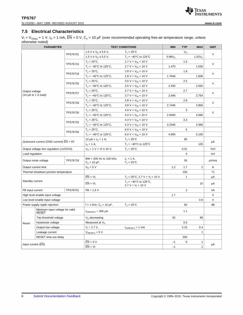
7.5 Electrical CharacteristicsVI = VO(typ) + 1 V, IO = 1 mA, EN = 0 V, Co = 10 µF (over recommended operating free-air temperature range, unlessotherwise noted)
PARAMETER TEST CONDITIONS MIN TYP MAX UNIT
1.5 V ≤ VO ≤ 5.5 V, TJ = 25°C VOTPS76701 V
1.5 V ≤ VO ≤ 5.5 V, TJ = −40°C to 125°C 0.98VO 1.02VO
TJ = 25°C, 2.7 V < VIN < 10 V 1.5TPS76715 V
TJ = −40°C to 125°C, 2.7 V < VIN < 10 V 1.470 1.530
TJ = 25°C, 2.8 V < VIN < 10 V 1.8TPS76718 V
TJ = −40°C to 125°C, 2.8 V < VIN < 10 V 1.7646 1.836
TJ = 25°C, 3.5 V < VIN < 10 V 2.5TPS76725 V
TJ = −40°C to 125°C, 3.5 V < VIN < 10 V 2.450 2.550
TJ = 25°C, 3.7 V < VIN < 10 V 2.7Output voltage TPS76727 V(10 µA to 1 A load) TJ = −40°C to 125°C, 3.7 V < VIN < 10 V 2.646 2.754
TJ = 25°C, 3.8 V < VIN < 10 V 2.8TPS76728 V
TJ = −40°C to 125°C, 3.8 V < VIN < 10 V 2.7446 2.856
TJ = 25°C, 4.0 V < VIN < 10 V 3TPS76730 V
TJ = −40°C to 125°C, 4.0 V < VIN < 10 V 2.9400 3.060
TJ = 25°C, 4.3 V < VIN < 10 V 3.3TPS76733
TJ = −40°C to 125°C, 4.3 V < VIN < 10 V 3.2346 3.366
TJ = 25°C, 6.0 V < VIN < 10 V 5TPS76750
TJ = −40°C to 125°C, 6.0 V < VIN < 10 V 4.900 5.100
10 µA < IO < 1 A, TJ = 25°C 85Quiescent current (GND current) EN = 0V µA
IO = 1 A, TJ = −40°C to 125°C 125
Output voltage line regulation (∆VO/VO) VO + 1 V < VI ≤ 10 V, TJ = 25°C 0.01 %/V
Load regulation 3 mV
BW = 200 Hz to 100 kHz, IC = 1 A,Output noise voltage TPS76718 55 µVrmsCo = 10 µF, TJ = 25°C
Output current limit VO = 0 V 1.2 1.7 2 A
Thermal shutdown junction temperature 150 °C
EN = VI, TJ = 25°C, 2.7 V < VI < 10 V 1 µAStandby current TJ = −40°C to 125°C,EN = VI, 10 µA2.7 V < VI < 10 V
FB input current TPS76701 FB = 1.5 V 2 nA
High level enable input voltage 1.7 V
Low level enable input voltage 0.9 V
Power supply ripple rejection f = 1 kHz, Co = 10 µF, TJ = 25°C 60 dB
Minimum input voltage for valid IO(RESET) = 300 μA 1.1RESET
Trip threshold voltage VO decreasing 92 98
Hysteresis voltage Measured at VO 0.5ResetOutput low voltage VI = 2.7 V, IO(RESET) = 1 mA 0.15 0.4
Leakage current V(RESET) = 5 V 1
RESET time-out delay 200
EN = 0 V –1 0 1Input current (EN) µA
EN = VI –1 1
6 Submit Documentation Feedback Copyright © 1999–2015, Texas Instruments Incorporated

VI
Vres(1) Vres
t
t
t
VO
Threshold
Voltage
RESET
Output 200 ms
Delay
200 ms
Delay
Output
Undefined
Output
Undefined
VIT+(2)
VIT−(2) VIT−
(2)
VIT+(2)
Less than 5% of the
output voltage
TPS767www.ti.com SLVS208J –MAY 1999–REVISED AUGUST 2015
Electrical Characteristics (continued)VI = VO(typ) + 1 V, IO = 1 mA, EN = 0 V, Co = 10 µF (over recommended operating free-air temperature range, unlessotherwise noted)
PARAMETER TEST CONDITIONS MIN TYP MAX UNIT
TJ = 25°C 500TPS76728 IO = 1 A mV
TJ = −40°C to 125°C 825
TJ = 25°C 450TPS76730 IO = 1 A mV
TJ = −40°C to 125°C 675Dropout voltage (1)
TJ = 25°C 350TPS76733 IO = 1 A mV
TJ = −40°C to 125°C 575
TJ = 25°C 230TPS76750 IO = 1 A mV
TJ = −40°C to 125°C 380
(1) IN voltage equals VO(typ) − 100 mV; TPS76701 output voltage set to 3.3 V nominal with external resistor divider. TPS76715, TPS76718,TPS76725, and TPS76727 dropout voltage limited by input voltage range limitations (i.e., TPS76730 input voltage needs to drop to 2.9V for purpose of this test).
Figure 1. Timing Diagram
Copyright © 1999–2015, Texas Instruments Incorporated Submit Documentation Feedback 7
IO − Output Current − A
1.4975
1.4960
1.4950
1.4970
1.4965
1.4955
1.4985
−O
utp
ut
Vo
ltag
e−
VV
O1.4980
0.1 0.30.2 0.8 10 0.90.4 0.5 0.6 0.7IO − Output Current − A
3.2830
3.2815
3.28000.1 0.3
3.2825
3.2820
3.2810
0.2 0.8 1
3.2835
0 0.9
−O
utp
ut
Vo
ltag
e−
VV
O
3.2805
0.4 0.5 0.6 0.7
TPS767SLVS208J –MAY 1999–REVISED AUGUST 2015 www.ti.com
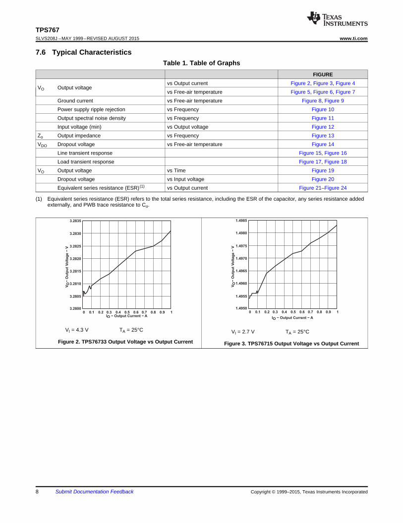
7.6 Typical CharacteristicsTable 1. Table of Graphs
FIGUREvs Output current Figure 2, Figure 3, Figure 4
VO Output voltagevs Free-air temperature Figure 5, Figure 6, Figure 7
Ground current vs Free-air temperature Figure 8, Figure 9Power supply ripple rejection vs Frequency Figure 10Output spectral noise density vs Frequency Figure 11Input voltage (min) vs Output voltage Figure 12
Zo Output impedance vs Frequency Figure 13VDO Dropout voltage vs Free-air temperature Figure 14
Line transient response Figure 15, Figure 16Load transient response Figure 17, Figure 18
VO Output voltage vs Time Figure 19Dropout voltage vs Input voltage Figure 20Equivalent series resistance (ESR) (1) vs Output current Figure 21–Figure 24
(1) Equivalent series resistance (ESR) refers to the total series resistance, including the ESR of the capacitor, any series resistance addedexternally, and PWB trace resistance to Co.
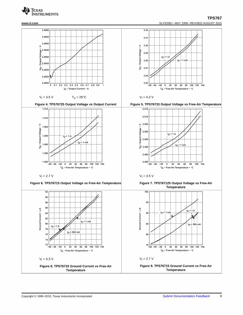
VI = 4.3 V TA = 25°C VI = 2.7 V TA = 25°C
Figure 2. TPS76733 Output Voltage vs Output Current Figure 3. TPS76715 Output Voltage vs Output Current
8 Submit Documentation Feedback Copyright © 1999–2015, Texas Instruments Incorporated
TA − Free-Air Temperature − °C
Gro
un
d C
urr
en
t−
Aμ
92
84
72
90
88
82
80
78
76
74
86
−40 0−20 100−60 12020 40 60 80 140
IO = 500 mA
IO = 1 A
IO = 1 mA
TA − Free-Air Temperature − °C
Gro
un
d C
urr
en
t−
Aμ
−40 0−20 100−60 12020 40 60 80 140
IO = 1 A
100
95
90
85
80
75
IO = 1 mA
IO = 500 mA
TA − Free-Air Temperature − °C
−O
utp
ut
Vo
ltag
e−
VV
O
1.515
1.500
1.485−40 0
1.510
1.505
1.495
−20 100−60 120
1.490
20 40 60 80
IO = 1 A
IO = 1 mA
140
TA − Free-Air Temperature − °C
−O
utp
ut
Vo
ltag
e−
VV
O
−40 0−20 100−60 12020 40 60 80
2.515
2.500
2.480
2.510
2.505
2.495
2.490
2.485
IO = 1 A
IO = 1 mA
IO − Output Current − A
2.4955
2.4940
2.49200.1 0.3
2.4950
2.4945
2.4935
0.2 0.4 0.6
2.4960
0 0.5
−O
utp
ut
Vo
ltag
e−
VV
O
2.4930
2.4925
0.80.7 0.9 1
TA − Free-Air Temperature − °C
−O
utp
ut
Vo
ltag
e−
VV
O
3.31
3.28
3.25−40 0
3.30
3.29
3.27
−20 100 140
3.32
−60 120
3.26
20 40 60 80
IO = 1 A
IO = 1 mA
TPS767www.ti.com SLVS208J –MAY 1999–REVISED AUGUST 2015
VI = 3.5 V TA = 25°C VI = 4.3 V
Figure 4. TPS76725 Output Voltage vs Output Current Figure 5. TPS76733 Output Voltage vs Free-Air Temperature
VI = 2.7 V VI = 3.5 V
Figure 6. TPS76715 Output Voltage vs Free-Air Temperature Figure 7. TPS767125 Output Voltage vs Free-AirTemperature
VI = 2.7 VVI = 4.3 V
Figure 9. TPS76715 Ground Current vs Free-AirFigure 8. TPS76733 Ground Current vs Free-AirTemperatureTemperature
Copyright © 1999–2015, Texas Instruments Incorporated Submit Documentation Feedback 9
TA − Free-Air Temperature − °C
−40 0 20 120
103
−60 40 60 80 100
−D
rop
ou
tV
olt
ag
e−
mV
VD
O
102
101
100
10−1
10−2−20 140
IO = 1 A
IO = 10 mA
IO = 0 VO
−C
han
ge in 10
0
3.7
2.7
VI
t − Time − μs
0 604020 80 100 140120 160 180 200
−In
pu
t V
olt
ag
e−
V∆
Ou
tpu
tV
olt
ag
e−
mV
−10
f − Frequency − kHz
−O
utp
ut
Imp
ed
an
ce
−Z
oΩ
101 102 105 106
0
10−1
10−2
104103
IO = 1 mA
IO = 1 A
3
2.7
21.5 1.75 2 2.25 2.5 2.75
−In
pu
t V
olt
ag
e (
Min
)−
V
4
3 3.25 3.5
TA = 25°C
VI
VO − Output Voltage − V
TA = 125°C
TA = −40°C
f − Frequency − Hz
102 103 104 105
10−5
10−6
10−8
10−7
IO = 7 mA
IO = 1 A
VH
zO
utp
ut
Sp
ectr
al
No
ise
Den
sit
y−
µ
100k10k
PS
RR
−P
ow
er
Su
pp
ly R
ipp
le R
eje
cti
on
−d
B
f − Frequency − Hz
60
50
40
30
20
10
0
−10
90
80
1k10010 1M
TPS767SLVS208J –MAY 1999–REVISED AUGUST 2015 www.ti.com
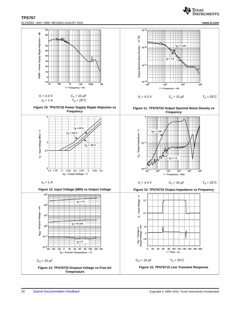
VI = 4.3 V Co = 10 µF VI = 4.3 V Co = 10 µF TA = 25°CIO = 1 A TA = 25°C
Figure 10. TPS76733 Power Supply Ripple Rejection vs Figure 11. TPS76733 Output Spectral Noise Density vsFrequency Frequency
IO = 1 A VI = 4.3 V Co = 10 µF TA = 25°C
Figure 12. Input Voltage (MIN) vs Output Voltage Figure 13. TPS76733 Output Impedance vs Frequency
CO = 10 µF TA = 25°CCO = 10 µF
Figure 15. TPS76715 Line Transient ResponseFigure 14. TPS76733 Dropout Voltage vs Free-AirTemperature
10 Submit Documentation Feedback Copyright © 1999–2015, Texas Instruments Incorporated
0.10 200 400 600 800 1000
10
IO − Output Current − mA
1
Region of Stability
Region of Instability
ES
R−
Eq
uiv
ale
nt
Seri
es R
esis
tan
ce
−Ω
VI − Input Voltage − V
600
300
03 4
500
400
200
3.52.5
−D
rop
ou
tV
olt
ag
e−
mV
100
4.5 5
VD
O
900
800
700
TA = 125°C
TA = −40°C
TA = 25°C
t − Time − μs
I−
Ou
tpu
t C
urr
en
t−
AO
VO
−C
han
ge
in
∆
Ou
tpu
tV
olt
ag
e−
mV
1
0.5
300200100 400 500 700600 800 900 10000
0
0
50
100
−50
−100
t − Time − ms
3
2
0.30.20.1 0.4 0.5 0.70.6 0.8 0.9 10
VO
−O
utp
ut
Vo
ltag
e−
V
0
1
4
En
ab
le P
uls
e−
V
0
t − Time − μs
I−
Ou
tpu
t C
urr
en
t−
AO
VO
−C
han
ge in
∆
Ou
tpu
tV
olt
ag
e−
mV
1
0.5
0
0 300200100 400 500 700600 800 900 1000
0
50
100
−50
−100
t − Time − μs
VO
−C
han
ge
in
VI
−In
pu
t V
olt
ag
e−
V∆
Ou
tpu
tV
olt
ag
e−
mV
5.3
604020 80 100 140120 160 180 2000
4.3
10
0
−10
TPS767www.ti.com SLVS208J –MAY 1999–REVISED AUGUST 2015
CO = 10 µF TA = 25°CCO = 10 µF TA = 25°C
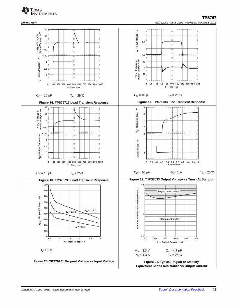
Figure 17. TPS76733 Line Transient ResponseFigure 16. TPS76715 Load Transient Response
CO = 10 µF IO = 1 A TA = 25°CCO = 10 µF TA = 25°C
Figure 19. TJPS7633 Output Voltage vs Time (At Startup)Figure 18. TPS76733 Load Transient Response
IO = 1 A VO = 3.3 V Co = 4.7 µFVI = 4.3 A TA = 25°C
Figure 20. TPS76701 Dropout Voltage vs Input Voltage Figure 21. Typical Region of StabilityEquivalent Series Resistance vs Output Current
Copyright © 1999–2015, Texas Instruments Incorporated Submit Documentation Feedback 11
IN
EN
OUT
+
GND
Co
ESR
RL
VITo Load
0.10 200 400 600 800 1000
10
1
IO − Output Current − mA
Region of Stability
Region of Instability
ES
R−
Eq
uiv
ale
nt
Seri
es R
esis
tan
ce
−Ω
IO − Output Current − mA
ES
R−
Eq
uiv
ale
nt
Seri
es R
esis
tan
ce
−Ω
0.10 200 400 600 800 1000
10
1
Region of Stability
Region of Instability
0.10 200 400 600 800 1000
10
IO − Output Current − mA
1
Region of Instability
Region of Stability
ES
R−
Eq
uiv
ale
nt
Seri
es
Resis
tan
ce
−Ω
TPS767SLVS208J –MAY 1999–REVISED AUGUST 2015 www.ti.com
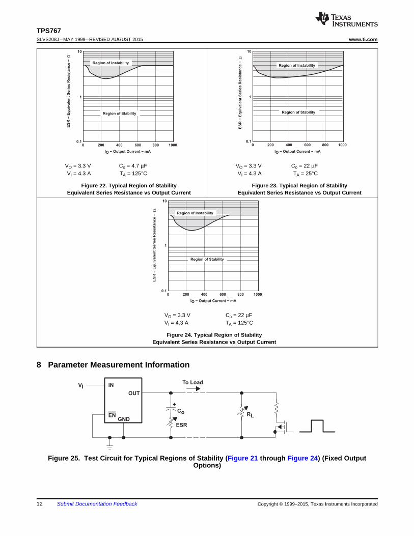
VO = 3.3 V Co = 4.7 µF VO = 3.3 V Co = 22 µFVI = 4.3 A TA = 125°C VI = 4.3 A TA = 25°C
Figure 22. Typical Region of Stability Figure 23. Typical Region of StabilityEquivalent Series Resistance vs Output Current Equivalent Series Resistance vs Output Current
VO = 3.3 V Co = 22 µFVI = 4.3 A TA = 125°C
Figure 24. Typical Region of StabilityEquivalent Series Resistance vs Output Current
8 Parameter Measurement Information
Figure 25. Test Circuit for Typical Regions of Stability (Figure 21 through Figure 24) (Fixed OutputOptions)
12 Submit Documentation Feedback Copyright © 1999–2015, Texas Instruments Incorporated
200 ms Delay
_
+
Vref = 1.1834 V
OUT
FB/NC
EN
GND
RESET
_
+
IN
External to the device
R1
R2
TPS767www.ti.com SLVS208J –MAY 1999–REVISED AUGUST 2015
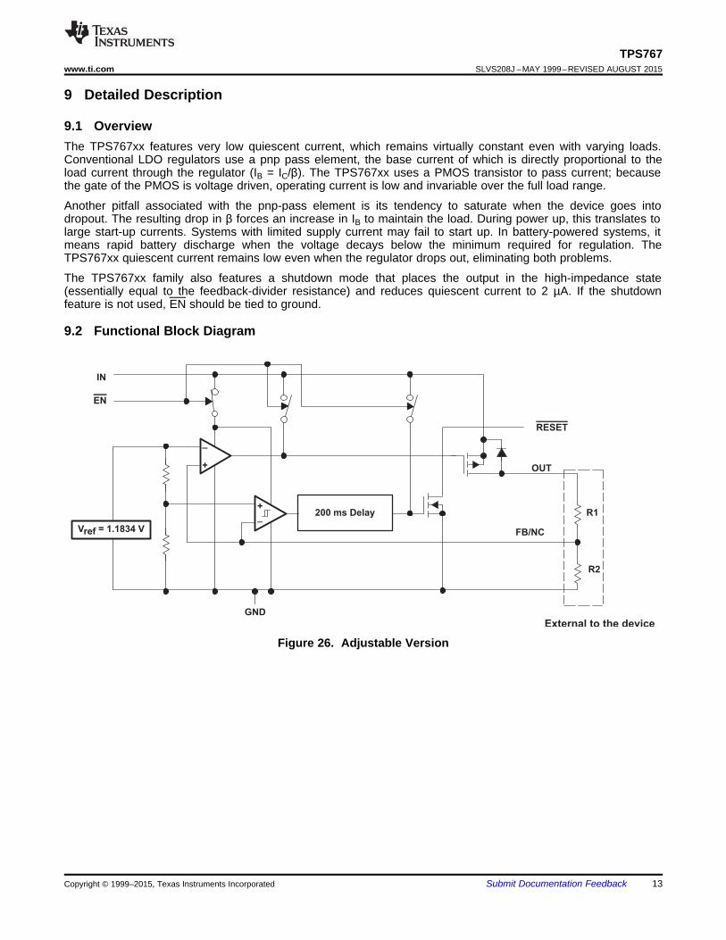
9 Detailed Description
9.1 OverviewThe TPS767xx features very low quiescent current, which remains virtually constant even with varying loads.Conventional LDO regulators use a pnp pass element, the base current of which is directly proportional to theload current through the regulator (IB = IC/β). The TPS767xx uses a PMOS transistor to pass current; becausethe gate of the PMOS is voltage driven, operating current is low and invariable over the full load range.
Another pitfall associated with the pnp-pass element is its tendency to saturate when the device goes intodropout. The resulting drop in β forces an increase in IB to maintain the load. During power up, this translates tolarge start-up currents. Systems with limited supply current may fail to start up. In battery-powered systems, itmeans rapid battery discharge when the voltage decays below the minimum required for regulation. TheTPS767xx quiescent current remains low even when the regulator drops out, eliminating both problems.
The TPS767xx family also features a shutdown mode that places the output in the high-impedance state(essentially equal to the feedback-divider resistance) and reduces quiescent current to 2 µA. If the shutdownfeature is not used, EN should be tied to ground.
9.2 Functional Block Diagram
Figure 26. Adjustable Version
Copyright © 1999–2015, Texas Instruments Incorporated Submit Documentation Feedback 13
_
+
Vref = 1.1834 V
OUT
EN
GND
R1
R2
RESET
_
+
IN
200 ms Delay
TPS767SLVS208J –MAY 1999–REVISED AUGUST 2015 www.ti.com
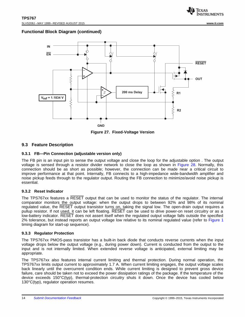
Functional Block Diagram (continued)
Figure 27. Fixed-Voltage Version
9.3 Feature Description
9.3.1 FB—Pin Connection (adjustable version only)The FB pin is an input pin to sense the output voltage and close the loop for the adjustable option . The outputvoltage is sensed through a resistor divider network to close the loop as shown in Figure 28. Normally, thisconnection should be as short as possible; however, the connection can be made near a critical circuit toimprove performance at that point. Internally, FB connects to a high-impedance wide-bandwidth amplifier andnoise pickup feeds through to the regulator output. Routing the FB connection to minimize/avoid noise pickup isessential.
9.3.2 Reset IndicatorThe TPS767xx features a RESET output that can be used to monitor the status of the regulator. The internalcomparator monitors the output voltage: when the output drops to between 92% and 98% of its nominalregulated value, the RESET output transistor turns on, taking the signal low. The open-drain output requires apullup resistor. If not used, it can be left floating. RESET can be used to drive power-on reset circuitry or as alow-battery indicator. RESET does not assert itself when the regulated output voltage falls outside the specified2% tolerance, but instead reports an output voltage low relative to its nominal regulated value (refer to Figure 1timing diagram for start-up sequence).
9.3.3 Regulator ProtectionThe TPS767xx PMOS-pass transistor has a built-in back diode that conducts reverse currents when the inputvoltage drops below the output voltage (e.g., during power down). Current is conducted from the output to theinput and is not internally limited. When extended reverse voltage is anticipated, external limiting may beappropriate.
The TPS767xx also features internal current limiting and thermal protection. During normal operation, theTPS767xx limits output current to approximately 1.7 A. When current limiting engages, the output voltage scalesback linearly until the overcurrent condition ends. While current limiting is designed to prevent gross devicefailure, care should be taken not to exceed the power dissipation ratings of the package. If the temperature of thedevice exceeds 150°C(typ), thermal-protection circuitry shuts it down. Once the device has cooled below130°C(typ), regulator operation resumes.
14 Submit Documentation Feedback Copyright © 1999–2015, Texas Instruments Incorporated
OUTPUT
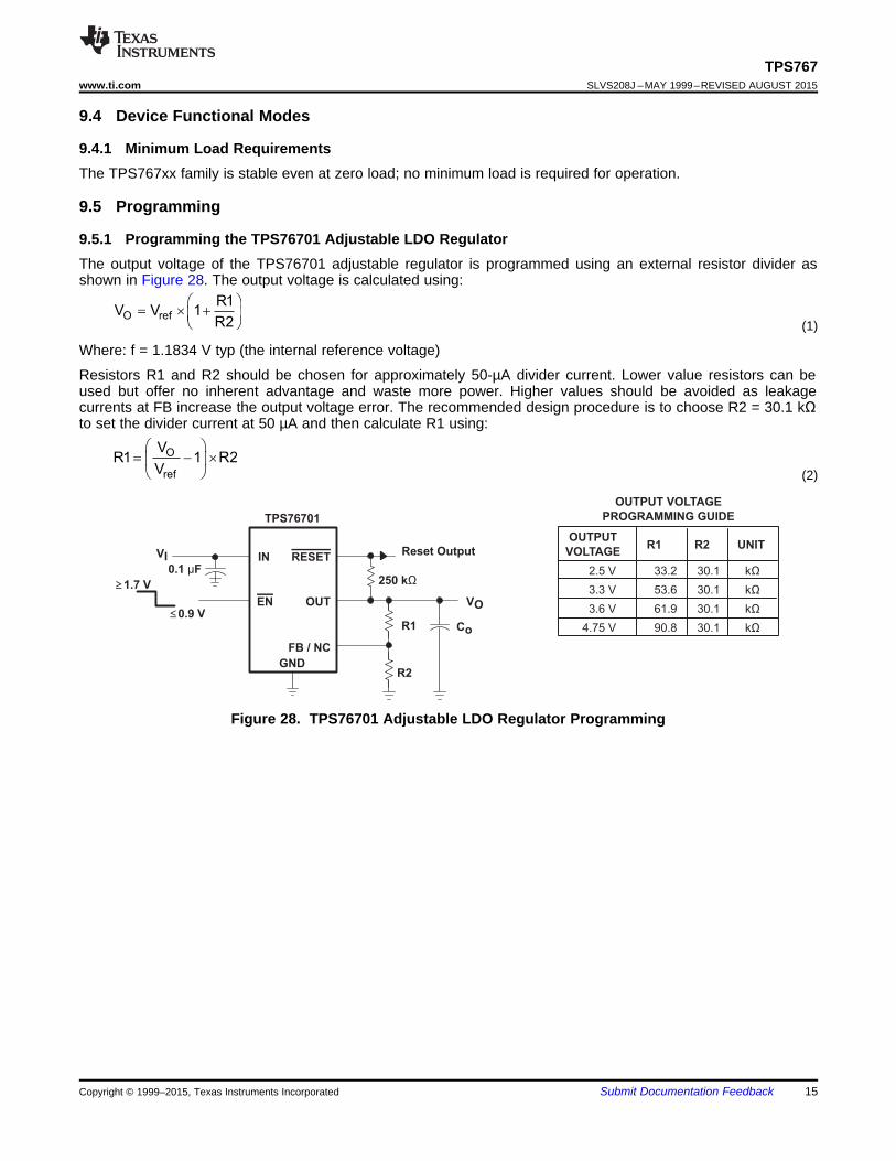
VOLTAGER1 R2
2.5 V
3.3 V
3.6 V
4.75 V
UNIT
33.2
53.6
61.9
90.8
30.1
30.1
30.1
30.1
kΩ
kΩ
kΩ
kΩ
OUTPUT VOLTAGE
PROGRAMMING GUIDE
VO
VI RESET
OUT
FB / NC
R1
R2GND
EN
IN
≤0.9 V
≥1.7 V
TPS76701
Reset Output
0.1 μF250 kΩ
Co
O
ref
VR1 1 R2
V
æ ö= - ´ç ÷
è ø
O ref
R1V V 1
R2
æ ö= ´ +ç ÷
è ø
TPS767www.ti.com SLVS208J –MAY 1999–REVISED AUGUST 2015
9.4 Device Functional Modes
9.4.1 Minimum Load RequirementsThe TPS767xx family is stable even at zero load; no minimum load is required for operation.
9.5 Programming
9.5.1 Programming the TPS76701 Adjustable LDO RegulatorThe output voltage of the TPS76701 adjustable regulator is programmed using an external resistor divider asshown in Figure 28. The output voltage is calculated using:
(1)
Where: f = 1.1834 V typ (the internal reference voltage)
Resistors R1 and R2 should be chosen for approximately 50-µA divider current. Lower value resistors can beused but offer no inherent advantage and waste more power. Higher values should be avoided as leakagecurrents at FB increase the output voltage error. The recommended design procedure is to choose R2 = 30.1 kΩto set the divider current at 50 µA and then calculate R1 using:
(2)
Figure 28. TPS76701 Adjustable LDO Regulator Programming
Copyright © 1999–2015, Texas Instruments Incorporated Submit Documentation Feedback 15
RESET
OUT
OUT
7
6
5
IN
IN
EN
GND
3
16
14
13
VI
C1
0.1 Fμ
RESET
VO
10 μF
+
TPS767xx
Co
250 kΩ
TPS767SLVS208J –MAY 1999–REVISED AUGUST 2015 www.ti.com
10 Application and Implementation
NOTEInformation in the following applications sections is not part of the TI componentspecification, and TI does not warrant its accuracy or completeness. TI’s customers areresponsible for determining suitability of components for their purposes. Customers shouldvalidate and test their design implementation to confirm system functionality.
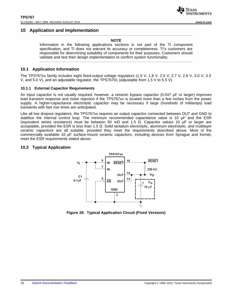
10.1 Application InformationThe TPS767xx family includes eight fixed-output voltage regulators (1.5 V, 1.8 V, 2.5 V, 2.7 V, 2.8 V, 3.0 V, 3.3V, and 5.0 V), and an adjustable regulator, the TPS76701 (adjustable from 1.5 V to 5.5 V).
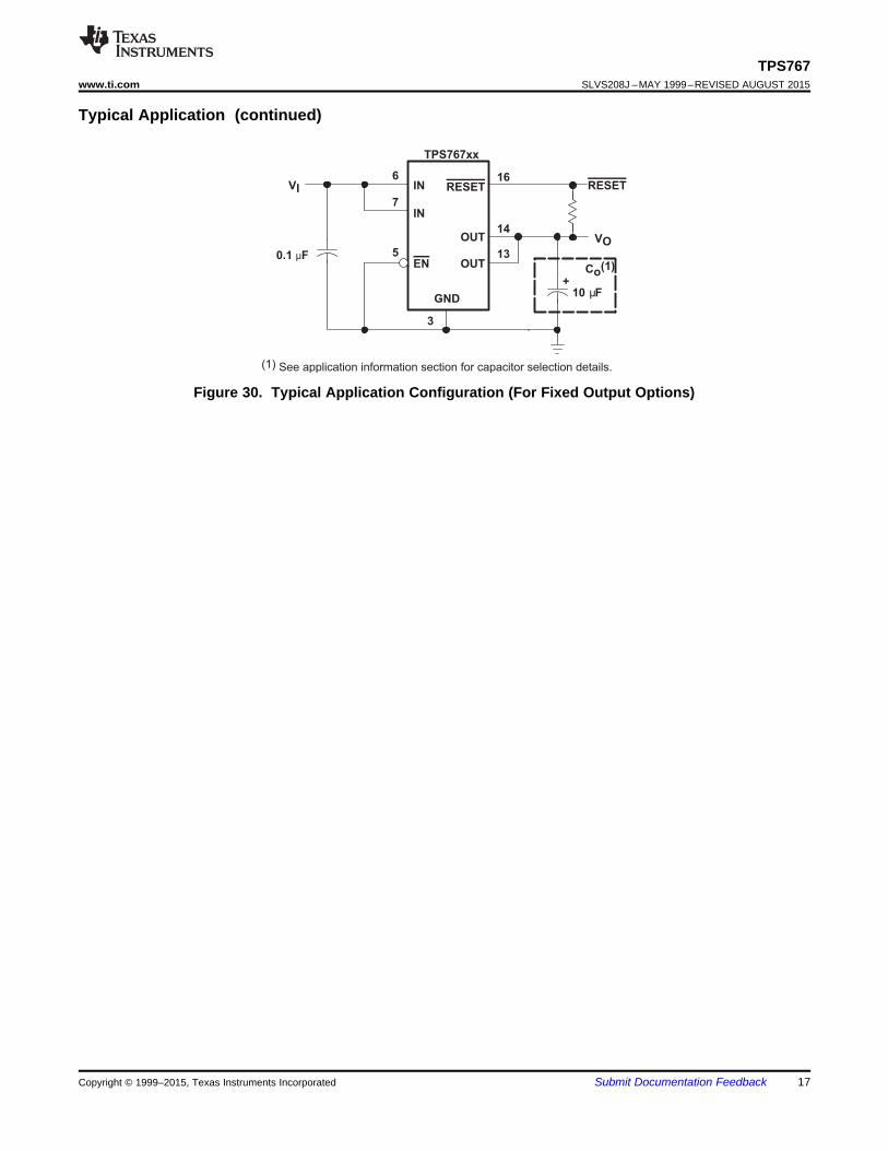
10.1.1 External Capacitor RequirementsAn input capacitor is not usually required; however, a ceramic bypass capacitor (0.047 µF or larger) improvesload transient response and noise rejection if the TPS767xx is located more than a few inches from the powersupply. A higher-capacitance electrolytic capacitor may be necessary if large (hundreds of milliamps) loadtransients with fast rise times are anticipated.
Like all low dropout regulators, the TPS767xx requires an output capacitor connected between OUT and GND tostabilize the internal control loop. The minimum recommended capacitance value is 10 µF and the ESR(equivalent series resistance) must be between 50 mΩ and 1.5 Ω. Capacitor values 10 µF or larger areacceptable, provided the ESR is less than 1.5 Ω. Solid tantalum electrolytic, aluminum electrolytic, and multilayerceramic capacitors are all suitable, provided they meet the requirements described above. Most of thecommercially available 10 µF surface-mount ceramic capacitors, including devices from Sprague and Kemet,meet the ESR requirements stated above.
10.2 Typical Application
Figure 29. Typical Application Circuit (Fixed Versions)
16 Submit Documentation Feedback Copyright © 1999–2015, Texas Instruments Incorporated
(1) See application information section for capacitor selection details.
RESET
OUT
OUT
7
6
5
IN
IN
EN
GND
3
16
14
13
VI
0.1 Fμ
RESET
VO
10 μF+
TPS767xx
Co(1)
TPS767www.ti.com SLVS208J –MAY 1999–REVISED AUGUST 2015
Typical Application (continued)
Figure 30. Typical Application Configuration (For Fixed Output Options)
Copyright © 1999–2015, Texas Instruments Incorporated Submit Documentation Feedback 17
( )D I O OP V V I= - ´
J AD(max)
JA
T max TP
Rq
-=
TPS767SLVS208J –MAY 1999–REVISED AUGUST 2015 www.ti.com
11 Layout
11.1 Power Dissipation and Junction TemperatureSpecified regulator operation is assured to a junction temperature of 125°C; the maximum junction temperatureshould be restricted to 125°C under normal operating conditions. This restriction limits the power dissipation theregulator can handle in any given application. To ensure the junction temperature is within acceptable limits,calculate the maximum allowable dissipation, PD(max), and the actual dissipation, PD, which must be less than orequal to PD(max).
The maximum-power-dissipation limit is determined using the following equation:
(3)
Where:TJmax is the maximum allowable junction temperature.RθJA is the thermal resistance junction-to-ambient for the package, i.e., 172°C/W for the 8-terminal SOIC andRθJA 32.6°C/W for the 20-terminal PWP with no airflow.TA is the ambient temperature.
The regulator dissipation is calculated using:
(4)
Power dissipation resulting from quiescent current is negligible. Excessive power dissipation will trigger thethermal protection circuit.
18 Submit Documentation Feedback Copyright © 1999–2015, Texas Instruments Incorporated
TPS767www.ti.com SLVS208J –MAY 1999–REVISED AUGUST 2015
12 Device and Documentation Support
12.1 Related LinksThe table below lists quick access links. Categories include technical documents, support and communityresources, tools and software, and quick access to sample or buy.
Table 2. Related LinksTECHNICAL TOOLS & SUPPORT &PARTS PRODUCT FOLDER SAMPLE & BUY DOCUMENTS SOFTWARE COMMUNITY
TPS76715 Click here Click here Click here Click here Click hereTPS76718 Click here Click here Click here Click here Click hereTPS76725 Click here Click here Click here Click here Click hereTPS76727 Click here Click here Click here Click here Click hereTPS76728 Click here Click here Click here Click here Click hereTPS76730 Click here Click here Click here Click here Click hereTPS76733 Click here Click here Click here Click here Click hereTPS76750 Click here Click here Click here Click here Click hereTPS76701 Click here Click here Click here Click here Click here
12.2 Community ResourcesThe following links connect to TI community resources. Linked contents are provided "AS IS" by the respectivecontributors. They do not constitute TI specifications and do not necessarily reflect TI's views; see TI's Terms ofUse.
TI E2E™ Online Community TI's Engineer-to-Engineer (E2E) Community. Created to foster collaborationamong engineers. At e2e.ti.com, you can ask questions, share knowledge, explore ideas and helpsolve problems with fellow engineers.
Design Support TI's Design Support Quickly find helpful E2E forums along with design support tools andcontact information for technical support.
12.3 TrademarksPowerPAD, E2E are trademarks of Texas Instruments.All other trademarks are the property of their respective owners.
12.4 Electrostatic Discharge CautionThese devices have limited built-in ESD protection. The leads should be shorted together or the device placed in conductive foamduring storage or handling to prevent electrostatic damage to the MOS gates.
12.5 GlossarySLYZ022 — TI Glossary.
This glossary lists and explains terms, acronyms, and definitions.
13 Mechanical, Packaging, and Orderable InformationThe following pages include mechanical, packaging, and orderable information. This information is the mostcurrent data available for the designated devices. This data is subject to change without notice and revision ofthis document. For browser-based versions of this data sheet, refer to the left-hand navigation.
Copyright © 1999–2015, Texas Instruments Incorporated Submit Documentation Feedback 19
PACKAGE OPTION ADDENDUM
www.ti.com 2-Jun-2017
Addendum-Page 1
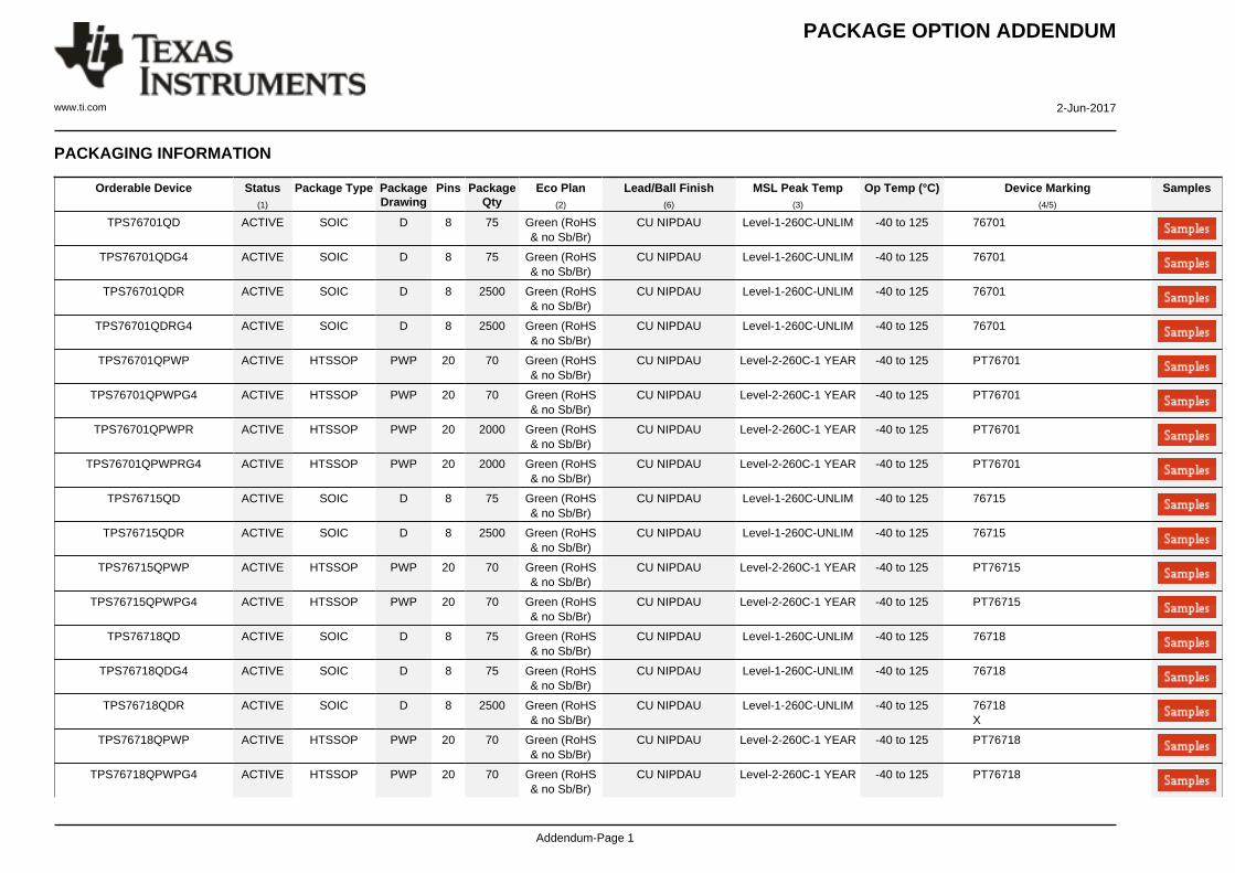
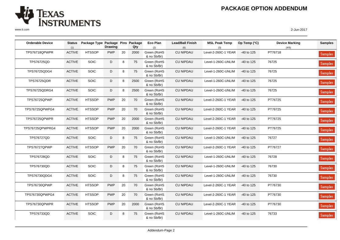
PACKAGING INFORMATION
Orderable Device Status(1)
Package Type PackageDrawing
Pins PackageQty
Eco Plan(2)
Lead/Ball Finish(6)
MSL Peak Temp(3)
Op Temp (°C) Device Marking(4/5)
Samples
TPS76701QD ACTIVE SOIC D 8 75 Green (RoHS& no Sb/Br)
CU NIPDAU Level-1-260C-UNLIM -40 to 125 76701
TPS76701QDG4 ACTIVE SOIC D 8 75 Green (RoHS& no Sb/Br)
CU NIPDAU Level-1-260C-UNLIM -40 to 125 76701
TPS76701QDR ACTIVE SOIC D 8 2500 Green (RoHS& no Sb/Br)
CU NIPDAU Level-1-260C-UNLIM -40 to 125 76701
TPS76701QDRG4 ACTIVE SOIC D 8 2500 Green (RoHS& no Sb/Br)
CU NIPDAU Level-1-260C-UNLIM -40 to 125 76701
TPS76701QPWP ACTIVE HTSSOP PWP 20 70 Green (RoHS& no Sb/Br)
CU NIPDAU Level-2-260C-1 YEAR -40 to 125 PT76701
TPS76701QPWPG4 ACTIVE HTSSOP PWP 20 70 Green (RoHS& no Sb/Br)
CU NIPDAU Level-2-260C-1 YEAR -40 to 125 PT76701
TPS76701QPWPR ACTIVE HTSSOP PWP 20 2000 Green (RoHS& no Sb/Br)
CU NIPDAU Level-2-260C-1 YEAR -40 to 125 PT76701
TPS76701QPWPRG4 ACTIVE HTSSOP PWP 20 2000 Green (RoHS& no Sb/Br)
CU NIPDAU Level-2-260C-1 YEAR -40 to 125 PT76701
TPS76715QD ACTIVE SOIC D 8 75 Green (RoHS& no Sb/Br)
CU NIPDAU Level-1-260C-UNLIM -40 to 125 76715
TPS76715QDR ACTIVE SOIC D 8 2500 Green (RoHS& no Sb/Br)
CU NIPDAU Level-1-260C-UNLIM -40 to 125 76715
TPS76715QPWP ACTIVE HTSSOP PWP 20 70 Green (RoHS& no Sb/Br)
CU NIPDAU Level-2-260C-1 YEAR -40 to 125 PT76715
TPS76715QPWPG4 ACTIVE HTSSOP PWP 20 70 Green (RoHS& no Sb/Br)
CU NIPDAU Level-2-260C-1 YEAR -40 to 125 PT76715
TPS76718QD ACTIVE SOIC D 8 75 Green (RoHS& no Sb/Br)
CU NIPDAU Level-1-260C-UNLIM -40 to 125 76718
TPS76718QDG4 ACTIVE SOIC D 8 75 Green (RoHS& no Sb/Br)
CU NIPDAU Level-1-260C-UNLIM -40 to 125 76718
TPS76718QDR ACTIVE SOIC D 8 2500 Green (RoHS& no Sb/Br)
CU NIPDAU Level-1-260C-UNLIM -40 to 125 76718X
TPS76718QPWP ACTIVE HTSSOP PWP 20 70 Green (RoHS& no Sb/Br)
CU NIPDAU Level-2-260C-1 YEAR -40 to 125 PT76718
TPS76718QPWPG4 ACTIVE HTSSOP PWP 20 70 Green (RoHS& no Sb/Br)
CU NIPDAU Level-2-260C-1 YEAR -40 to 125 PT76718
PACKAGE OPTION ADDENDUM
www.ti.com 2-Jun-2017
Addendum-Page 2
Orderable Device Status(1)
Package Type PackageDrawing
Pins PackageQty
Eco Plan(2)
Lead/Ball Finish(6)
MSL Peak Temp(3)
Op Temp (°C) Device Marking(4/5)
Samples
TPS76718QPWPR ACTIVE HTSSOP PWP 20 2000 Green (RoHS& no Sb/Br)
CU NIPDAU Level-2-260C-1 YEAR -40 to 125 PT76718
TPS76725QD ACTIVE SOIC D 8 75 Green (RoHS& no Sb/Br)
CU NIPDAU Level-1-260C-UNLIM -40 to 125 76725
TPS76725QDG4 ACTIVE SOIC D 8 75 Green (RoHS& no Sb/Br)
CU NIPDAU Level-1-260C-UNLIM -40 to 125 76725
TPS76725QDR ACTIVE SOIC D 8 2500 Green (RoHS& no Sb/Br)
CU NIPDAU Level-1-260C-UNLIM -40 to 125 76725
TPS76725QDRG4 ACTIVE SOIC D 8 2500 Green (RoHS& no Sb/Br)
CU NIPDAU Level-1-260C-UNLIM -40 to 125 76725
TPS76725QPWP ACTIVE HTSSOP PWP 20 70 Green (RoHS& no Sb/Br)
CU NIPDAU Level-2-260C-1 YEAR -40 to 125 PT76725
TPS76725QPWPG4 ACTIVE HTSSOP PWP 20 70 Green (RoHS& no Sb/Br)
CU NIPDAU Level-2-260C-1 YEAR -40 to 125 PT76725
TPS76725QPWPR ACTIVE HTSSOP PWP 20 2000 Green (RoHS& no Sb/Br)
CU NIPDAU Level-2-260C-1 YEAR -40 to 125 PT76725
TPS76725QPWPRG4 ACTIVE HTSSOP PWP 20 2000 Green (RoHS& no Sb/Br)
CU NIPDAU Level-2-260C-1 YEAR -40 to 125 PT76725
TPS76727QD ACTIVE SOIC D 8 75 Green (RoHS& no Sb/Br)
CU NIPDAU Level-1-260C-UNLIM -40 to 125 76727
TPS76727QPWP ACTIVE HTSSOP PWP 20 70 Green (RoHS& no Sb/Br)
CU NIPDAU Level-2-260C-1 YEAR -40 to 125 PT76727
TPS76728QD ACTIVE SOIC D 8 75 Green (RoHS& no Sb/Br)
CU NIPDAU Level-1-260C-UNLIM -40 to 125 76728
TPS76730QD ACTIVE SOIC D 8 75 Green (RoHS& no Sb/Br)
CU NIPDAU Level-1-260C-UNLIM -40 to 125 76730
TPS76730QDG4 ACTIVE SOIC D 8 75 Green (RoHS& no Sb/Br)
CU NIPDAU Level-1-260C-UNLIM -40 to 125 76730
TPS76730QPWP ACTIVE HTSSOP PWP 20 70 Green (RoHS& no Sb/Br)
CU NIPDAU Level-2-260C-1 YEAR -40 to 125 PT76730
TPS76730QPWPG4 ACTIVE HTSSOP PWP 20 70 Green (RoHS& no Sb/Br)
CU NIPDAU Level-2-260C-1 YEAR -40 to 125 PT76730
TPS76730QPWPR ACTIVE HTSSOP PWP 20 2000 Green (RoHS& no Sb/Br)
CU NIPDAU Level-2-260C-1 YEAR -40 to 125 PT76730
TPS76733QD ACTIVE SOIC D 8 75 Green (RoHS& no Sb/Br)
CU NIPDAU Level-1-260C-UNLIM -40 to 125 76733
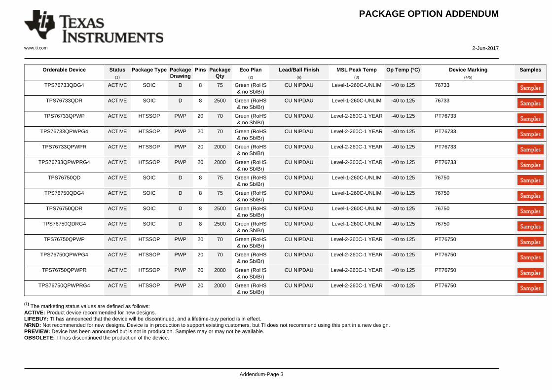
PACKAGE OPTION ADDENDUM
www.ti.com 2-Jun-2017
Addendum-Page 3
Orderable Device Status(1)
Package Type PackageDrawing
Pins PackageQty
Eco Plan(2)
Lead/Ball Finish(6)
MSL Peak Temp(3)
Op Temp (°C) Device Marking(4/5)
Samples
TPS76733QDG4 ACTIVE SOIC D 8 75 Green (RoHS& no Sb/Br)
CU NIPDAU Level-1-260C-UNLIM -40 to 125 76733
TPS76733QDR ACTIVE SOIC D 8 2500 Green (RoHS& no Sb/Br)
CU NIPDAU Level-1-260C-UNLIM -40 to 125 76733
TPS76733QPWP ACTIVE HTSSOP PWP 20 70 Green (RoHS& no Sb/Br)
CU NIPDAU Level-2-260C-1 YEAR -40 to 125 PT76733
TPS76733QPWPG4 ACTIVE HTSSOP PWP 20 70 Green (RoHS& no Sb/Br)
CU NIPDAU Level-2-260C-1 YEAR -40 to 125 PT76733
TPS76733QPWPR ACTIVE HTSSOP PWP 20 2000 Green (RoHS& no Sb/Br)
CU NIPDAU Level-2-260C-1 YEAR -40 to 125 PT76733
TPS76733QPWPRG4 ACTIVE HTSSOP PWP 20 2000 Green (RoHS& no Sb/Br)
CU NIPDAU Level-2-260C-1 YEAR -40 to 125 PT76733
TPS76750QD ACTIVE SOIC D 8 75 Green (RoHS& no Sb/Br)
CU NIPDAU Level-1-260C-UNLIM -40 to 125 76750
TPS76750QDG4 ACTIVE SOIC D 8 75 Green (RoHS& no Sb/Br)
CU NIPDAU Level-1-260C-UNLIM -40 to 125 76750
TPS76750QDR ACTIVE SOIC D 8 2500 Green (RoHS& no Sb/Br)
CU NIPDAU Level-1-260C-UNLIM -40 to 125 76750
TPS76750QDRG4 ACTIVE SOIC D 8 2500 Green (RoHS& no Sb/Br)
CU NIPDAU Level-1-260C-UNLIM -40 to 125 76750
TPS76750QPWP ACTIVE HTSSOP PWP 20 70 Green (RoHS& no Sb/Br)
CU NIPDAU Level-2-260C-1 YEAR -40 to 125 PT76750
TPS76750QPWPG4 ACTIVE HTSSOP PWP 20 70 Green (RoHS& no Sb/Br)
CU NIPDAU Level-2-260C-1 YEAR -40 to 125 PT76750
TPS76750QPWPR ACTIVE HTSSOP PWP 20 2000 Green (RoHS& no Sb/Br)
CU NIPDAU Level-2-260C-1 YEAR -40 to 125 PT76750
TPS76750QPWPRG4 ACTIVE HTSSOP PWP 20 2000 Green (RoHS& no Sb/Br)
CU NIPDAU Level-2-260C-1 YEAR -40 to 125 PT76750
(1) The marketing status values are defined as follows:ACTIVE: Product device recommended for new designs.LIFEBUY: TI has announced that the device will be discontinued, and a lifetime-buy period is in effect.NRND: Not recommended for new designs. Device is in production to support existing customers, but TI does not recommend using this part in a new design.PREVIEW: Device has been announced but is not in production. Samples may or may not be available.OBSOLETE: TI has discontinued the production of the device.
PACKAGE OPTION ADDENDUM
www.ti.com 2-Jun-2017
Addendum-Page 4
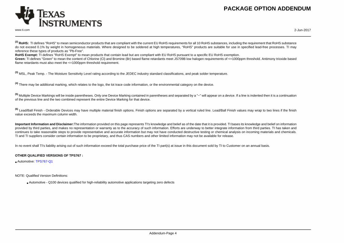
(2) RoHS: TI defines "RoHS" to mean semiconductor products that are compliant with the current EU RoHS requirements for all 10 RoHS substances, including the requirement that RoHS substancedo not exceed 0.1% by weight in homogeneous materials. Where designed to be soldered at high temperatures, "RoHS" products are suitable for use in specified lead-free processes. TI mayreference these types of products as "Pb-Free".RoHS Exempt: TI defines "RoHS Exempt" to mean products that contain lead but are compliant with EU RoHS pursuant to a specific EU RoHS exemption.Green: TI defines "Green" to mean the content of Chlorine (Cl) and Bromine (Br) based flame retardants meet JS709B low halogen requirements of <=1000ppm threshold. Antimony trioxide basedflame retardants must also meet the <=1000ppm threshold requirement.
(3) MSL, Peak Temp. - The Moisture Sensitivity Level rating according to the JEDEC industry standard classifications, and peak solder temperature.
(4) There may be additional marking, which relates to the logo, the lot trace code information, or the environmental category on the device.
(5) Multiple Device Markings will be inside parentheses. Only one Device Marking contained in parentheses and separated by a "~" will appear on a device. If a line is indented then it is a continuationof the previous line and the two combined represent the entire Device Marking for that device.
(6) Lead/Ball Finish - Orderable Devices may have multiple material finish options. Finish options are separated by a vertical ruled line. Lead/Ball Finish values may wrap to two lines if the finishvalue exceeds the maximum column width.
Important Information and Disclaimer:The information provided on this page represents TI's knowledge and belief as of the date that it is provided. TI bases its knowledge and belief on informationprovided by third parties, and makes no representation or warranty as to the accuracy of such information. Efforts are underway to better integrate information from third parties. TI has taken andcontinues to take reasonable steps to provide representative and accurate information but may not have conducted destructive testing or chemical analysis on incoming materials and chemicals.TI and TI suppliers consider certain information to be proprietary, and thus CAS numbers and other limited information may not be available for release.
In no event shall TI's liability arising out of such information exceed the total purchase price of the TI part(s) at issue in this document sold by TI to Customer on an annual basis.
OTHER QUALIFIED VERSIONS OF TPS767 :
• Automotive: TPS767-Q1
NOTE: Qualified Version Definitions:
• Automotive - Q100 devices qualified for high-reliability automotive applications targeting zero defects
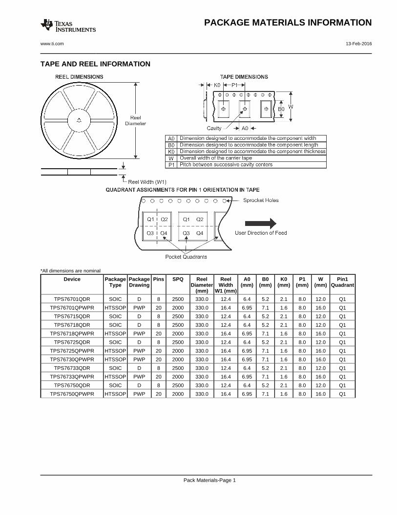
TAPE AND REEL INFORMATION
*All dimensions are nominal
Device PackageType
PackageDrawing
Pins SPQ ReelDiameter
(mm)
ReelWidth
W1 (mm)
A0(mm)
B0(mm)
K0(mm)
P1(mm)
W(mm)
Pin1Quadrant
TPS76701QDR SOIC D 8 2500 330.0 12.4 6.4 5.2 2.1 8.0 12.0 Q1
TPS76701QPWPR HTSSOP PWP 20 2000 330.0 16.4 6.95 7.1 1.6 8.0 16.0 Q1
TPS76715QDR SOIC D 8 2500 330.0 12.4 6.4 5.2 2.1 8.0 12.0 Q1
TPS76718QDR SOIC D 8 2500 330.0 12.4 6.4 5.2 2.1 8.0 12.0 Q1
TPS76718QPWPR HTSSOP PWP 20 2000 330.0 16.4 6.95 7.1 1.6 8.0 16.0 Q1
TPS76725QDR SOIC D 8 2500 330.0 12.4 6.4 5.2 2.1 8.0 12.0 Q1
TPS76725QPWPR HTSSOP PWP 20 2000 330.0 16.4 6.95 7.1 1.6 8.0 16.0 Q1
TPS76730QPWPR HTSSOP PWP 20 2000 330.0 16.4 6.95 7.1 1.6 8.0 16.0 Q1
TPS76733QDR SOIC D 8 2500 330.0 12.4 6.4 5.2 2.1 8.0 12.0 Q1
TPS76733QPWPR HTSSOP PWP 20 2000 330.0 16.4 6.95 7.1 1.6 8.0 16.0 Q1
TPS76750QDR SOIC D 8 2500 330.0 12.4 6.4 5.2 2.1 8.0 12.0 Q1
TPS76750QPWPR HTSSOP PWP 20 2000 330.0 16.4 6.95 7.1 1.6 8.0 16.0 Q1
PACKAGE MATERIALS INFORMATION
www.ti.com 13-Feb-2016
Pack Materials-Page 1
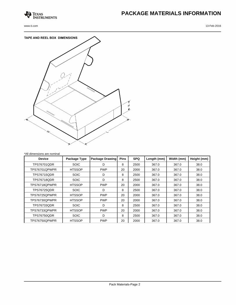
*All dimensions are nominal
Device Package Type Package Drawing Pins SPQ Length (mm) Width (mm) Height (mm)
TPS76701QDR SOIC D 8 2500 367.0 367.0 38.0
TPS76701QPWPR HTSSOP PWP 20 2000 367.0 367.0 38.0
TPS76715QDR SOIC D 8 2500 367.0 367.0 38.0
TPS76718QDR SOIC D 8 2500 367.0 367.0 38.0
TPS76718QPWPR HTSSOP PWP 20 2000 367.0 367.0 38.0
TPS76725QDR SOIC D 8 2500 367.0 367.0 38.0
TPS76725QPWPR HTSSOP PWP 20 2000 367.0 367.0 38.0
TPS76730QPWPR HTSSOP PWP 20 2000 367.0 367.0 38.0
TPS76733QDR SOIC D 8 2500 367.0 367.0 38.0
TPS76733QPWPR HTSSOP PWP 20 2000 367.0 367.0 38.0
TPS76750QDR SOIC D 8 2500 367.0 367.0 38.0
TPS76750QPWPR HTSSOP PWP 20 2000 367.0 367.0 38.0
PACKAGE MATERIALS INFORMATION
www.ti.com 13-Feb-2016
Pack Materials-Page 2
IMPORTANT NOTICE
Texas Instruments Incorporated (TI) reserves the right to make corrections, enhancements, improvements and other changes to itssemiconductor products and services per JESD46, latest issue, and to discontinue any product or service per JESD48, latest issue. Buyersshould obtain the latest relevant information before placing orders and should verify that such information is current and complete.TI’s published terms of sale for semiconductor products (http://www.ti.com/sc/docs/stdterms.htm) apply to the sale of packaged integratedcircuit products that TI has qualified and released to market. Additional terms may apply to the use or sale of other types of TI products andservices.Reproduction of significant portions of TI information in TI data sheets is permissible only if reproduction is without alteration and isaccompanied by all associated warranties, conditions, limitations, and notices. TI is not responsible or liable for such reproduceddocumentation. Information of third parties may be subject to additional restrictions. Resale of TI products or services with statementsdifferent from or beyond the parameters stated by TI for that product or service voids all express and any implied warranties for theassociated TI product or service and is an unfair and deceptive business practice. TI is not responsible or liable for any such statements.Buyers and others who are developing systems that incorporate TI products (collectively, “Designers”) understand and agree that Designersremain responsible for using their independent analysis, evaluation and judgment in designing their applications and that Designers havefull and exclusive responsibility to assure the safety of Designers' applications and compliance of their applications (and of all TI productsused in or for Designers’ applications) with all applicable regulations, laws and other applicable requirements. Designer represents that, withrespect to their applications, Designer has all the necessary expertise to create and implement safeguards that (1) anticipate dangerousconsequences of failures, (2) monitor failures and their consequences, and (3) lessen the likelihood of failures that might cause harm andtake appropriate actions. Designer agrees that prior to using or distributing any applications that include TI products, Designer willthoroughly test such applications and the functionality of such TI products as used in such applications.TI’s provision of technical, application or other design advice, quality characterization, reliability data or other services or information,including, but not limited to, reference designs and materials relating to evaluation modules, (collectively, “TI Resources”) are intended toassist designers who are developing applications that incorporate TI products; by downloading, accessing or using TI Resources in anyway, Designer (individually or, if Designer is acting on behalf of a company, Designer’s company) agrees to use any particular TI Resourcesolely for this purpose and subject to the terms of this Notice.TI’s provision of TI Resources does not expand or otherwise alter TI’s applicable published warranties or warranty disclaimers for TIproducts, and no additional obligations or liabilities arise from TI providing such TI Resources. TI reserves the right to make corrections,enhancements, improvements and other changes to its TI Resources. TI has not conducted any testing other than that specificallydescribed in the published documentation for a particular TI Resource.Designer is authorized to use, copy and modify any individual TI Resource only in connection with the development of applications thatinclude the TI product(s) identified in such TI Resource. NO OTHER LICENSE, EXPRESS OR IMPLIED, BY ESTOPPEL OR OTHERWISETO ANY OTHER TI INTELLECTUAL PROPERTY RIGHT, AND NO LICENSE TO ANY TECHNOLOGY OR INTELLECTUAL PROPERTYRIGHT OF TI OR ANY THIRD PARTY IS GRANTED HEREIN, including but not limited to any patent right, copyright, mask work right, orother intellectual property right relating to any combination, machine, or process in which TI products or services are used. Informationregarding or referencing third-party products or services does not constitute a license to use such products or services, or a warranty orendorsement thereof. Use of TI Resources may require a license from a third party under the patents or other intellectual property of thethird party, or a license from TI under the patents or other intellectual property of TI.TI RESOURCES ARE PROVIDED “AS IS” AND WITH ALL FAULTS. TI DISCLAIMS ALL OTHER WARRANTIES ORREPRESENTATIONS, EXPRESS OR IMPLIED, REGARDING RESOURCES OR USE THEREOF, INCLUDING BUT NOT LIMITED TOACCURACY OR COMPLETENESS, TITLE, ANY EPIDEMIC FAILURE WARRANTY AND ANY IMPLIED WARRANTIES OFMERCHANTABILITY, FITNESS FOR A PARTICULAR PURPOSE, AND NON-INFRINGEMENT OF ANY THIRD PARTY INTELLECTUALPROPERTY RIGHTS. TI SHALL NOT BE LIABLE FOR AND SHALL NOT DEFEND OR INDEMNIFY DESIGNER AGAINST ANY CLAIM,INCLUDING BUT NOT LIMITED TO ANY INFRINGEMENT CLAIM THAT RELATES TO OR IS BASED ON ANY COMBINATION OFPRODUCTS EVEN IF DESCRIBED IN TI RESOURCES OR OTHERWISE. IN NO EVENT SHALL TI BE LIABLE FOR ANY ACTUAL,DIRECT, SPECIAL, COLLATERAL, INDIRECT, PUNITIVE, INCIDENTAL, CONSEQUENTIAL OR EXEMPLARY DAMAGES INCONNECTION WITH OR ARISING OUT OF TI RESOURCES OR USE THEREOF, AND REGARDLESS OF WHETHER TI HAS BEENADVISED OF THE POSSIBILITY OF SUCH DAMAGES.Unless TI has explicitly designated an individual product as meeting the requirements of a particular industry standard (e.g., ISO/TS 16949and ISO 26262), TI is not responsible for any failure to meet such industry standard requirements.Where TI specifically promotes products as facilitating functional safety or as compliant with industry functional safety standards, suchproducts are intended to help enable customers to design and create their own applications that meet applicable functional safety standardsand requirements. Using products in an application does not by itself establish any safety features in the application. Designers mustensure compliance with safety-related requirements and standards applicable to their applications. Designer may not use any TI products inlife-critical medical equipment unless authorized officers of the parties have executed a special contract specifically governing such use.Life-critical medical equipment is medical equipment where failure of such equipment would cause serious bodily injury or death (e.g., lifesupport, pacemakers, defibrillators, heart pumps, neurostimulators, and implantables). Such equipment includes, without limitation, allmedical devices identified by the U.S. Food and Drug Administration as Class III devices and equivalent classifications outside the U.S.TI may expressly designate certain products as completing a particular qualification (e.g., Q100, Military Grade, or Enhanced Product).Designers agree that it has the necessary expertise to select the product with the appropriate qualification designation for their applicationsand that proper product selection is at Designers’ own risk. Designers are solely responsible for compliance with all legal and regulatoryrequirements in connection with such selection.Designer will fully indemnify TI and its representatives against any damages, costs, losses, and/or liabilities arising out of Designer’s non-compliance with the terms and provisions of this Notice.
Mailing Address: Texas Instruments, Post Office Box 655303, Dallas, Texas 75265Copyright © 2017, Texas Instruments Incorporated