TPDxF003 Four-, Six-, and Eight-Channel EMI Filters With … · · 2018-02-16Ch5_Out Ch6_Out...
27
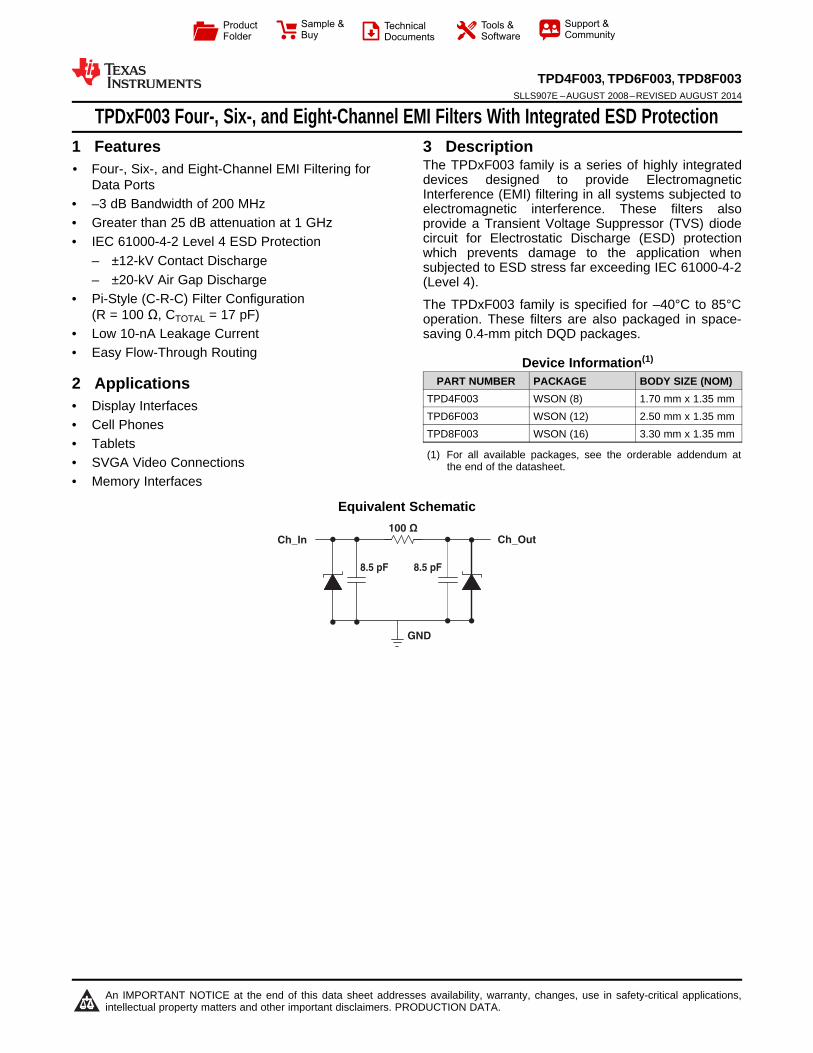
100 Ω GND Ch_In Ch_Out 8.5 pF 8.5 pF Product Folder Sample & Buy Technical Documents Tools & Software Support & Community TPD4F003, TPD6F003, TPD8F003 SLLS907E – AUGUST 2008 – REVISED AUGUST 2014 TPDxF003 Four-, Six-, and Eight-Channel EMI Filters With Integrated ESD Protection 1 Features 3 Description The TPDxF003 family is a series of highly integrated 1• Four-, Six-, and Eight-Channel EMI Filtering for devices designed to provide Electromagnetic Data Ports Interference (EMI) filtering in all systems subjected to • –3 dB Bandwidth of 200 MHz electromagnetic interference. These filters also • Greater than 25 dB attenuation at 1 GHz provide a Transient Voltage Suppressor (TVS) diode circuit for Electrostatic Discharge (ESD) protection • IEC 61000-4-2 Level 4 ESD Protection which prevents damage to the application when – ±12-kV Contact Discharge subjected to ESD stress far exceeding IEC 61000-4-2 – ±20-kV Air Gap Discharge (Level 4). • Pi-Style (C-R-C) Filter Configuration The TPDxF003 family is specified for –40°C to 85°C (R = 100 Ω,C TOTAL = 17 pF) operation. These filters are also packaged in space- • Low 10-nA Leakage Current saving 0.4-mm pitch DQD packages. • Easy Flow-Through Routing Device Information (1) PART NUMBER PACKAGE BODY SIZE (NOM) 2 Applications TPD4F003 WSON (8) 1.70 mm x 1.35 mm • Display Interfaces TPD6F003 WSON (12) 2.50 mm x 1.35 mm • Cell Phones TPD8F003 WSON (16) 3.30 mm x 1.35 mm • Tablets (1) For all available packages, see the orderable addendum at • SVGA Video Connections the end of the datasheet. • Memory Interfaces Equivalent Schematic 1 An IMPORTANT NOTICE at the end of this data sheet addresses availability, warranty, changes, use in safety-critical applications, intellectual property matters and other important disclaimers. PRODUCTION DATA.
Transcript of TPDxF003 Four-, Six-, and Eight-Channel EMI Filters With … · · 2018-02-16Ch5_Out Ch6_Out...
100 Ω
GND
Ch_In Ch_Out
8.5 pF 8.5 pF
Product
Folder
Sample &Buy
Technical
Documents
Tools &
Software
Support &Community
TPD4F003, TPD6F003, TPD8F003SLLS907E –AUGUST 2008–REVISED AUGUST 2014
TPDxF003 Four-, Six-, and Eight-Channel EMI Filters With Integrated ESD Protection1 Features 3 Description
The TPDxF003 family is a series of highly integrated1• Four-, Six-, and Eight-Channel EMI Filtering for
devices designed to provide ElectromagneticData PortsInterference (EMI) filtering in all systems subjected to
• –3 dB Bandwidth of 200 MHz electromagnetic interference. These filters also• Greater than 25 dB attenuation at 1 GHz provide a Transient Voltage Suppressor (TVS) diode
circuit for Electrostatic Discharge (ESD) protection• IEC 61000-4-2 Level 4 ESD Protectionwhich prevents damage to the application when– ±12-kV Contact Discharge subjected to ESD stress far exceeding IEC 61000-4-2
– ±20-kV Air Gap Discharge (Level 4).• Pi-Style (C-R-C) Filter Configuration The TPDxF003 family is specified for –40°C to 85°C
(R = 100 Ω, CTOTAL = 17 pF) operation. These filters are also packaged in space-• Low 10-nA Leakage Current saving 0.4-mm pitch DQD packages.• Easy Flow-Through Routing
Device Information(1)
PART NUMBER PACKAGE BODY SIZE (NOM)2 ApplicationsTPD4F003 WSON (8) 1.70 mm x 1.35 mm• Display InterfacesTPD6F003 WSON (12) 2.50 mm x 1.35 mm
• Cell PhonesTPD8F003 WSON (16) 3.30 mm x 1.35 mm
• Tablets(1) For all available packages, see the orderable addendum at• SVGA Video Connections the end of the datasheet.
• Memory Interfaces
Equivalent Schematic
1
An IMPORTANT NOTICE at the end of this data sheet addresses availability, warranty, changes, use in safety-critical applications,intellectual property matters and other important disclaimers. PRODUCTION DATA.
TPD4F003, TPD6F003, TPD8F003SLLS907E –AUGUST 2008–REVISED AUGUST 2014 www.ti.com
Table of Contents7.3 Feature Description................................................... 71 Features .................................................................. 17.4 Device Functional Modes.......................................... 82 Applications ........................................................... 1
8 Applications and Implementation ........................ 93 Description ............................................................. 18.1 Application Information.............................................. 94 Revision History..................................................... 28.2 Typical Application .................................................... 95 Pin Configuration and Functions ......................... 3
9 Power Supply Recommendations ...................... 116 Specifications......................................................... 410 Layout................................................................... 116.1 Absolute Maximum Ratings ..................................... 4
10.1 Layout Guidelines ................................................. 116.2 Handling Ratings....................................................... 410.2 Layout Example .................................................... 116.3 Recommended Operating Conditions....................... 4
11 Device and Documentation Support ................. 126.4 Thermal Information .................................................. 411.1 Related Links ........................................................ 126.5 Electrical Characteristics........................................... 411.2 Trademarks ........................................................... 126.6 Typical Characteristics .............................................. 511.3 Electrostatic Discharge Caution............................ 127 Detailed Description .............................................. 711.4 Glossary ................................................................ 127.1 Overview ................................................................... 7
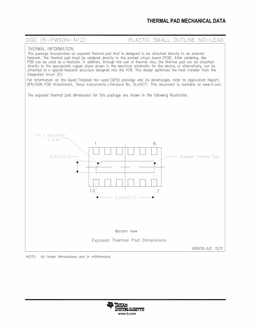
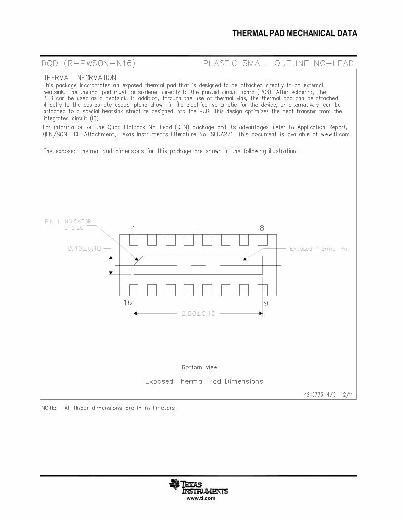
12 Mechanical, Packaging, and Orderable7.2 Functional Block Diagram ......................................... 7Information ........................................................... 12
4 Revision History
Changes from Revision D (January 2010) to Revision E Page
• Added Handling Rating table, Feature Description section, Device Functional Modes, Application andImplementation section, Power Supply Recommendations section, Layout section, Device and DocumentationSupport section, and Mechanical, Packaging, and Orderable Information section ............................................................... 1
2 Submit Documentation Feedback Copyright © 2008–2014, Texas Instruments Incorporated
Product Folder Links: TPD4F003 TPD6F003 TPD8F003
Ch1_In 161
Ch2_In 152
Ch3_In 143
Ch4_In 134
Ch5_In 125
Ch6_In 116
Ch1_Out
Ch2_Out
Ch3_Out
Ch4_Out
Ch5_Out
Ch6_Out
Ch7_In 107
Ch8_In
GN
D
98
Ch7_Out
Ch8_Out
TPD8F003
3.3 mm x 1.35 mm x 0.75 mm(0.4-mm pitch)
Ch1_In 121
Ch2_In 112
Ch3_In 103
Ch4_In 94
Ch5_In 85
Ch6_In 76
Ch1_Out
Ch2_Out
Ch3_Out
Ch4_Out
Ch5_Out
Ch6_Out
GN
D
TPD6F003
2.5 mm x 1.35 mm x 0.75 mm(0.4-mm pitch)
Ch1_In 81
Ch2_In 72
Ch3_In 63
Ch4_In 54
Ch1_Out
Ch2_Out
Ch3_Out
Ch4_Out
GN
DTPD4F003
1.7 mm x 1.35 mm x 0.75 mm(0.4-mm pitch)
TPD4F003, TPD6F003, TPD8F003www.ti.com SLLS907E –AUGUST 2008–REVISED AUGUST 2014
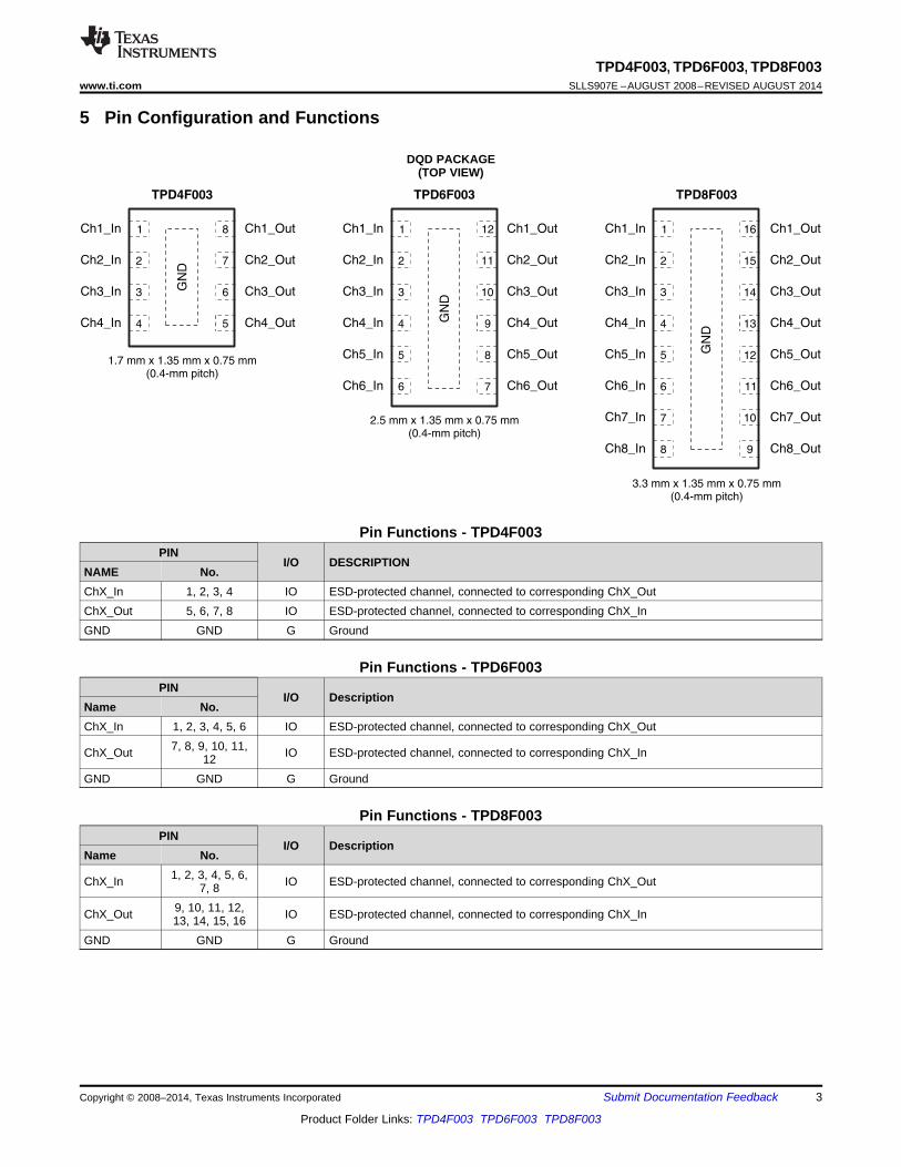
5 Pin Configuration and Functions
DQD PACKAGE(TOP VIEW)
Pin Functions - TPD4F003PIN
I/O DESCRIPTIONNAME No.ChX_In 1, 2, 3, 4 IO ESD-protected channel, connected to corresponding ChX_OutChX_Out 5, 6, 7, 8 IO ESD-protected channel, connected to corresponding ChX_InGND GND G Ground
Pin Functions - TPD6F003PIN
I/O DescriptionName No.ChX_In 1, 2, 3, 4, 5, 6 IO ESD-protected channel, connected to corresponding ChX_Out
7, 8, 9, 10, 11,ChX_Out IO ESD-protected channel, connected to corresponding ChX_In12GND GND G Ground
Pin Functions - TPD8F003PIN
I/O DescriptionName No.
1, 2, 3, 4, 5, 6,ChX_In IO ESD-protected channel, connected to corresponding ChX_Out7, 89, 10, 11, 12,ChX_Out IO ESD-protected channel, connected to corresponding ChX_In13, 14, 15, 16
GND GND G Ground
Copyright © 2008–2014, Texas Instruments Incorporated Submit Documentation Feedback 3
Product Folder Links: TPD4F003 TPD6F003 TPD8F003
TPD4F003, TPD6F003, TPD8F003SLLS907E –AUGUST 2008–REVISED AUGUST 2014 www.ti.com
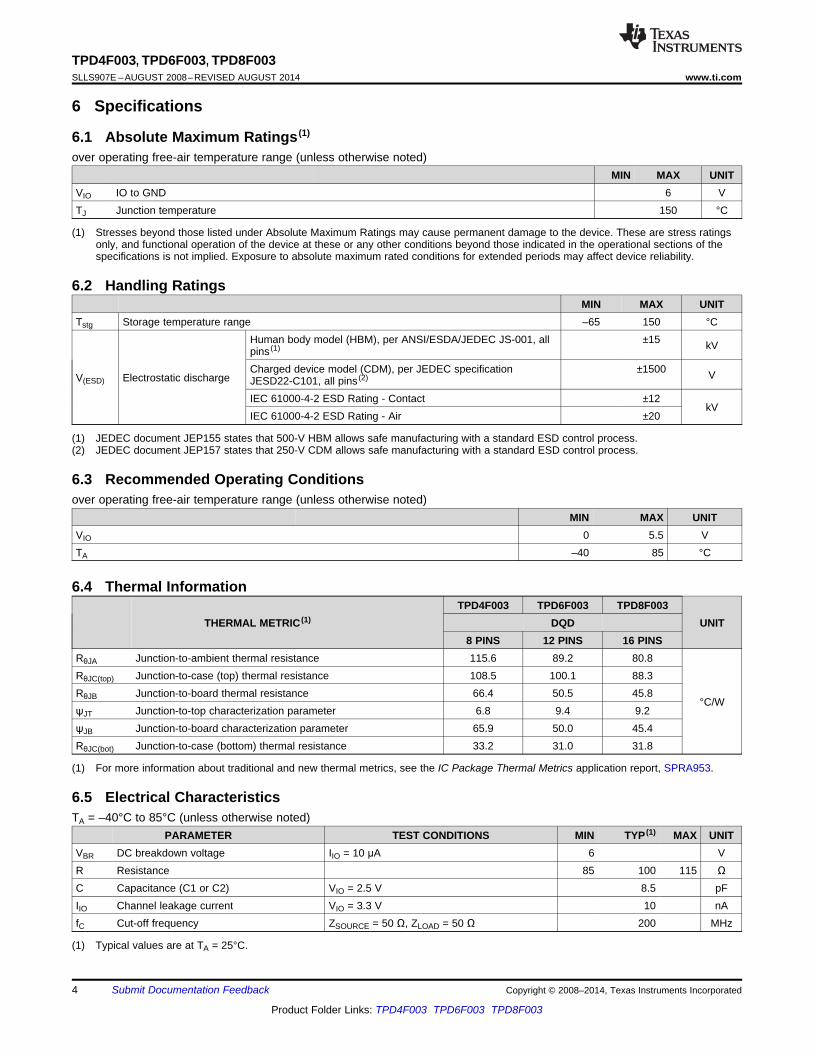
6 Specifications
6.1 Absolute Maximum Ratings (1)
over operating free-air temperature range (unless otherwise noted)MIN MAX UNIT
VIO IO to GND 6 VTJ Junction temperature 150 °C
(1) Stresses beyond those listed under Absolute Maximum Ratings may cause permanent damage to the device. These are stress ratingsonly, and functional operation of the device at these or any other conditions beyond those indicated in the operational sections of thespecifications is not implied. Exposure to absolute maximum rated conditions for extended periods may affect device reliability.
6.2 Handling RatingsMIN MAX UNIT
Tstg Storage temperature range –65 150 °CHuman body model (HBM), per ANSI/ESDA/JEDEC JS-001, all ±15 kVpins (1)
Charged device model (CDM), per JEDEC specification ±1500 VV(ESD) Electrostatic discharge JESD22-C101, all pins (2)
IEC 61000-4-2 ESD Rating - Contact ±12kV
IEC 61000-4-2 ESD Rating - Air ±20
(1) JEDEC document JEP155 states that 500-V HBM allows safe manufacturing with a standard ESD control process.(2) JEDEC document JEP157 states that 250-V CDM allows safe manufacturing with a standard ESD control process.
6.3 Recommended Operating Conditionsover operating free-air temperature range (unless otherwise noted)
MIN MAX UNITVIO 0 5.5 VTA –40 85 °C
6.4 Thermal InformationTPD4F003 TPD6F003 TPD8F003
THERMAL METRIC (1) DQD UNIT8 PINS 12 PINS 16 PINS
RθJA Junction-to-ambient thermal resistance 115.6 89.2 80.8RθJC(top) Junction-to-case (top) thermal resistance 108.5 100.1 88.3RθJB Junction-to-board thermal resistance 66.4 50.5 45.8
°C/WψJT Junction-to-top characterization parameter 6.8 9.4 9.2ψJB Junction-to-board characterization parameter 65.9 50.0 45.4RθJC(bot) Junction-to-case (bottom) thermal resistance 33.2 31.0 31.8
(1) For more information about traditional and new thermal metrics, see the IC Package Thermal Metrics application report, SPRA953.
6.5 Electrical CharacteristicsTA = –40°C to 85°C (unless otherwise noted)
PARAMETER TEST CONDITIONS MIN TYP (1) MAX UNITVBR DC breakdown voltage IIO = 10 μA 6 VR Resistance 85 100 115 ΩC Capacitance (C1 or C2) VIO = 2.5 V 8.5 pFIIO Channel leakage current VIO = 3.3 V 10 nAfC Cut-off frequency ZSOURCE = 50 Ω, ZLOAD = 50 Ω 200 MHz
(1) Typical values are at TA = 25°C.
4 Submit Documentation Feedback Copyright © 2008–2014, Texas Instruments Incorporated
Product Folder Links: TPD4F003 TPD6F003 TPD8F003

-0.001
-0.0008
-0.0006
-0.0004
-0.0002
0
0.0002
0.0004
0.0006
0.0008
0.001
-4 -2 0 2 4 6 8
Voltage (V)
Curr
ent(m
A)
-50
-45
-40
-35
-30
-25
-20
-15
-10
-5
0
1.00E+06 1.00E+07 1.00E+08 1.00E+09 1.00E+10
Frequency (Hz)
Insert
ion
Loss
(dB
)
TPD8F003 TPD6F003 TPD4F003
TPD8F003
3dB drop/Bias of 0.0V
-3dB = 198MHz
Peak/Freq/Db = 2.57/45 GHz/dB
TPD6F003
3dB drop/Bias of 0.0V
-3dB = 197MHz
Peak/Freq/Db = 2.30/47 GHz/dB
TPD4F003
3dB drop/Bias of 0.0V
-3dB = 197MHz
Peak/Freq/Db = 2.25/45 GHz/dB
-140
-120
-100
-80
-60
-40
-20
0
20
40
0 25 50 75 100 125 150 175 200
Time (ns)
Am
plit
ud
e(V
)
Ch_In Ch_Out
-140
-120
-100
-80
-60
-40
-20
0
20
40
0 25 50 75 100 125 150 175 200
Time (ns)
Am
plit
ud
e(V
)
Ch_In Ch_Out
-40
-20
0
20
40
60
80
100
120
140
0 25 50 75 100 125 150 175 200
Time (ns)
Am
plit
ud
e(V
)
Ch_In Ch_Out
-40
-20
0
20
40
60
80
100
120
140
0 25 50 75 100 125 150 175 200
Time (ns)
Am
plit
ud
e(V
)
Ch_In Ch_Out
TPD4F003, TPD6F003, TPD8F003www.ti.com SLLS907E –AUGUST 2008–REVISED AUGUST 2014
6.6 Typical Characteristics
6.6.1 IEC Clamping Waveforms(clamp voltage measured both at Ch_Out and Ch_In)
Figure 2. With 12 kV Contact ESD Stress at Ch_OutFigure 1. With 8 kV Contact ESD Stress at Ch_Out
Figure 3. With -8 kV Contact ESD Stress at Ch_Out Figure 4. With -12 kV Contact ESD Stress at Ch_Out
Figure 6. DC Voltage-Current Sweep Across Input/OutputFigure 5. Frequency ResponsePins
Copyright © 2008–2014, Texas Instruments Incorporated Submit Documentation Feedback 5
Product Folder Links: TPD4F003 TPD6F003 TPD8F003
-110
-105
-100
-95
-90
-85
-80
-75
-70
-65
-60
-55
-50
-45
-40
-35
-30
-25
-20
-15
-10
-5
0
1.00E+05 1.00E+06 1.00E+07 1.00E+08 1.00E+09 1.00E+10
Frequency (Hz)
Cro
ssta
lk(d
B)
Adjacent Signal pair Farthest Signal Pair
-110
-105
-100
-95
-90
-85
-80
-75
-70
-65
-60
-55
-50
-45
-40
-35
-30
-25
-20
-15
-10
-5
0
1.00E+05 1.00E+06 1.00E+07 1.00E+08 1.00E+09 1.00E+10
Frequency (Hz)
Cro
ssta
lk(d
B)
Adjacent Signal Pair Farthest Signal Pair
-110
-105
-100
-95
-90
-85
-80
-75
-70
-65
-60
-55
-50
-45
-40
-35
-30
-25
-20
-15
-10
-5
0
1.00E+05 1.00E+06 1.00E+07 1.00E+08 1.00E+09 1.00E+10
Frequency (Hz)
Cro
ssta
lk(d
B)
Adjacent Signal Pair Farthest Signal Pair
TPD4F003, TPD6F003, TPD8F003SLLS907E –AUGUST 2008–REVISED AUGUST 2014 www.ti.com
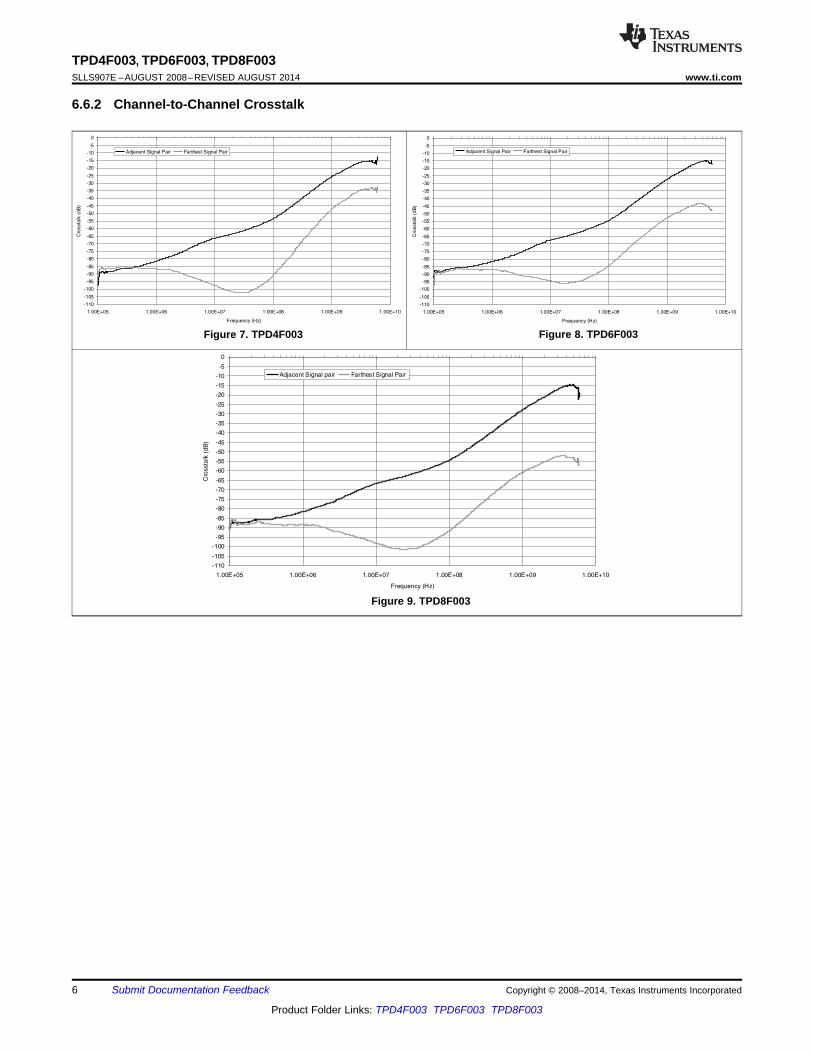
6.6.2 Channel-to-Channel Crosstalk
Figure 8. TPD6F003Figure 7. TPD4F003
Figure 9. TPD8F003
6 Submit Documentation Feedback Copyright © 2008–2014, Texas Instruments Incorporated
Product Folder Links: TPD4F003 TPD6F003 TPD8F003
100 Ω
GND
Ch_In Ch_Out
8.5 pF 8.5 pF
TPD4F003, TPD6F003, TPD8F003www.ti.com SLLS907E –AUGUST 2008–REVISED AUGUST 2014
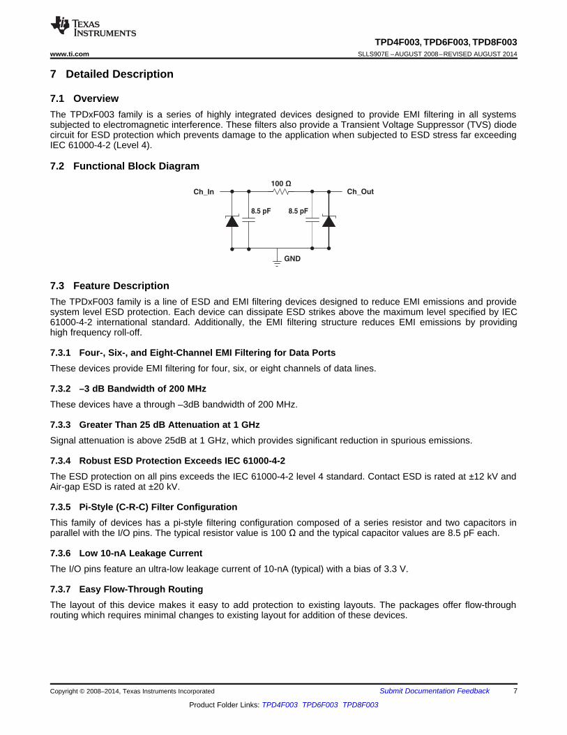
7 Detailed Description
7.1 OverviewThe TPDxF003 family is a series of highly integrated devices designed to provide EMI filtering in all systemssubjected to electromagnetic interference. These filters also provide a Transient Voltage Suppressor (TVS) diodecircuit for ESD protection which prevents damage to the application when subjected to ESD stress far exceedingIEC 61000-4-2 (Level 4).
7.2 Functional Block Diagram
7.3 Feature DescriptionThe TPDxF003 family is a line of ESD and EMI filtering devices designed to reduce EMI emissions and providesystem level ESD protection. Each device can dissipate ESD strikes above the maximum level specified by IEC61000-4-2 international standard. Additionally, the EMI filtering structure reduces EMI emissions by providinghigh frequency roll-off.
7.3.1 Four-, Six-, and Eight-Channel EMI Filtering for Data PortsThese devices provide EMI filtering for four, six, or eight channels of data lines.
7.3.2 –3 dB Bandwidth of 200 MHzThese devices have a through –3dB bandwidth of 200 MHz.
7.3.3 Greater Than 25 dB Attenuation at 1 GHzSignal attenuation is above 25dB at 1 GHz, which provides significant reduction in spurious emissions.
7.3.4 Robust ESD Protection Exceeds IEC 61000-4-2The ESD protection on all pins exceeds the IEC 61000-4-2 level 4 standard. Contact ESD is rated at ±12 kV andAir-gap ESD is rated at ±20 kV.
7.3.5 Pi-Style (C-R-C) Filter ConfigurationThis family of devices has a pi-style filtering configuration composed of a series resistor and two capacitors inparallel with the I/O pins. The typical resistor value is 100 Ω and the typical capacitor values are 8.5 pF each.
7.3.6 Low 10-nA Leakage CurrentThe I/O pins feature an ultra-low leakage current of 10-nA (typical) with a bias of 3.3 V.
7.3.7 Easy Flow-Through RoutingThe layout of this device makes it easy to add protection to existing layouts. The packages offer flow-throughrouting which requires minimal changes to existing layout for addition of these devices.
Copyright © 2008–2014, Texas Instruments Incorporated Submit Documentation Feedback 7
Product Folder Links: TPD4F003 TPD6F003 TPD8F003
TPD4F003, TPD6F003, TPD8F003SLLS907E –AUGUST 2008–REVISED AUGUST 2014 www.ti.com
7.4 Device Functional ModesThe TPDxF003 family of devices are passive integrated circuits that passively filter EMI and trigger whenvoltages are above VBR or below the lower diode voltage (–0.6 V). During ESD events, voltages as high as ±20kV (air) can be directed to ground via the internal diode network. Once the voltages on the protected line fallbelow the trigger levels, the device reverts to passive.
8 Submit Documentation Feedback Copyright © 2008–2014, Texas Instruments Incorporated
Product Folder Links: TPD4F003 TPD6F003 TPD8F003

1
2
3
4
5
6 7
8
12
11
10
9
GND
TPD6F003
1
2
3
4
5
6 7
8
12
11
10
9
GND
TPD6F003
1
2
3
4
5
6 7
8
12
11
10
9
GND
TPD6F003
Con
nect
or
Dis
play
Pan
el C
onne
ctor
R0
R1
R2
R3
R4
R5
G0
G1
G2
G3
G4
G5
B0
B1
B2
B3
B4
B5
TPD4F003, TPD6F003, TPD8F003www.ti.com SLLS907E –AUGUST 2008–REVISED AUGUST 2014
8 Applications and Implementation
8.1 Application InformationThe TPDxF003 family are diode type TVS' integrated with series resistors for filtering emitted EMI. As signalpasses through the device, higher frequency components are filtered out. This device also provides a path toground during ESD events and isolates the protected IC. As the current from ESD passes through the TVS, onlya small voltage drop is present across the diode. This is the voltage presented to the protected IC. In particular,these filters are ideal for EMI filtering and protecting data lines from ESD at the display, keypad, and memoryinterfaces.
8.2 Typical Application
Figure 10. Display Panel Schematic
Copyright © 2008–2014, Texas Instruments Incorporated Submit Documentation Feedback 9
Product Folder Links: TPD4F003 TPD6F003 TPD8F003
±50
±45
±40
±35
±30
±25
±20
±15
±10
±5
0
1.E+05 1.E+06 1.E+07 1.E+08 1.E+09 1.E+10
Inse
rtio
n Lo
ss (
dB)
Frequency (Hz)
Channel 1
Channel 2
Channel 3
Channel 4
Channel 5
Channel 6
C001
TPD4F003, TPD6F003, TPD8F003SLLS907E –AUGUST 2008–REVISED AUGUST 2014 www.ti.com
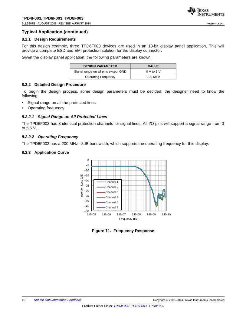
Typical Application (continued)8.2.1 Design RequirementsFor this design example, three TPD6F003 devices are used in an 18-bit display panel application. This willprovide a complete ESD and EMI protection solution for the display connector.
Given the display panel application, the following parameters are known.
DESIGN PARAMETER VALUESignal range on all pins except GND 0 V to 5 V
Operating Frequency 100 MHz
8.2.2 Detailed Design ProcedureTo begin the design process, some design parameters must be decided; the designer need to know thefollowing:
• Signal range on all the protected lines• Operating frequency
8.2.2.1 Signal Range on All Protected LinesThe TPD6F003 has 8 identical protection channels for signal lines. All I/O pins will support a signal range from 0to 5.5 V.
8.2.2.2 Operating FrequencyThe TPD6F003 has a 200 MHz –3dB bandwidth, which supports the operating frequency for this display.
8.2.3 Application Curve
Figure 11. Frequency Response
10 Submit Documentation Feedback Copyright © 2008–2014, Texas Instruments Incorporated
Product Folder Links: TPD4F003 TPD6F003 TPD8F003
123456
121110987
GND
123456
121110987
GND
123456
121110987
GND
R0
R1
R2
R3
R4
R5
G0
G1
G2
G3
G4
G5
B0
B1
B2
B3
B4
B5
VIA to GND Plane
TPD4F003, TPD6F003, TPD8F003www.ti.com SLLS907E –AUGUST 2008–REVISED AUGUST 2014
9 Power Supply Recommendations
This family of devices are passive EMI and ESD devices so there is no need to power them. Care should betaken to not violate the recommended VIO specification (5.5 V) to ensure the device functions properly.
10 Layout
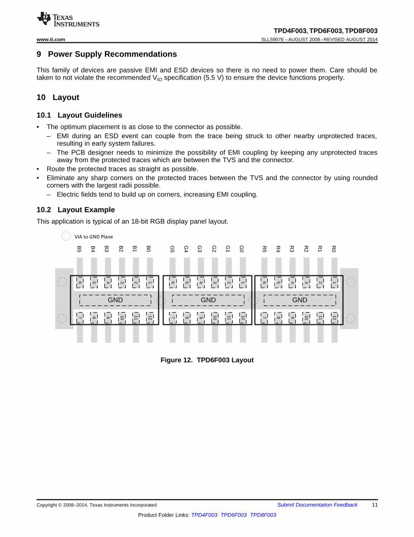
10.1 Layout Guidelines• The optimum placement is as close to the connector as possible.
– EMI during an ESD event can couple from the trace being struck to other nearby unprotected traces,resulting in early system failures.
– The PCB designer needs to minimize the possibility of EMI coupling by keeping any unprotected tracesaway from the protected traces which are between the TVS and the connector.
• Route the protected traces as straight as possible.• Eliminate any sharp corners on the protected traces between the TVS and the connector by using rounded
corners with the largest radii possible.– Electric fields tend to build up on corners, increasing EMI coupling.
10.2 Layout ExampleThis application is typical of an 18-bit RGB display panel layout.
Figure 12. TPD6F003 Layout
Copyright © 2008–2014, Texas Instruments Incorporated Submit Documentation Feedback 11
Product Folder Links: TPD4F003 TPD6F003 TPD8F003
TPD4F003, TPD6F003, TPD8F003SLLS907E –AUGUST 2008–REVISED AUGUST 2014 www.ti.com
11 Device and Documentation Support
11.1 Related LinksThe table below lists quick access links. Categories include technical documents, support and communityresources, tools and software, and quick access to sample or buy.
Table 1. Related LinksTECHNICAL TOOLS & SUPPORT &PARTS PRODUCT FOLDER SAMPLE & BUY DOCUMENTS SOFTWARE COMMUNITY
TPD4F003 Click here Click here Click here Click here Click hereTPD6F003 Click here Click here Click here Click here Click hereTPD8F003 Click here Click here Click here Click here Click here
11.2 TrademarksAll trademarks are the property of their respective owners.
11.3 Electrostatic Discharge CautionThese devices have limited built-in ESD protection. The leads should be shorted together or the device placed in conductive foamduring storage or handling to prevent electrostatic damage to the MOS gates.
11.4 GlossarySLYZ022 — TI Glossary.
This glossary lists and explains terms, acronyms, and definitions.
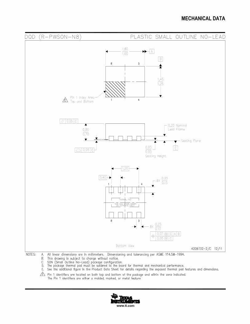
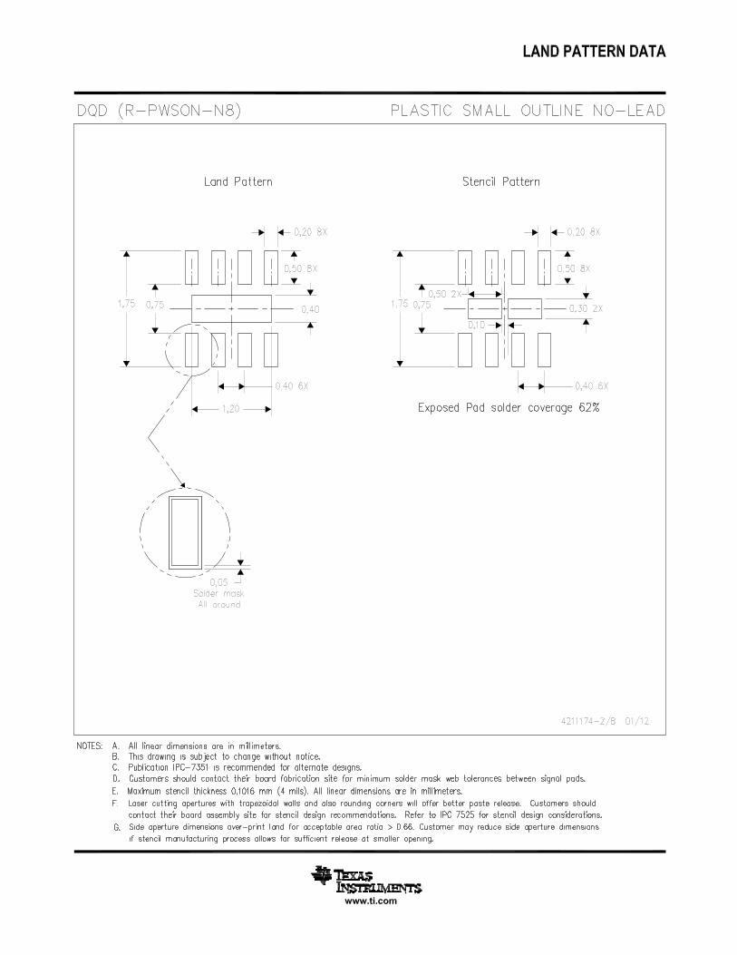
12 Mechanical, Packaging, and Orderable InformationThe following pages include mechanical, packaging, and orderable information. This information is the mostcurrent data available for the designated devices. This data is subject to change without notice and revision ofthis document. For browser-based versions of this data sheet, refer to the left-hand navigation.
12 Submit Documentation Feedback Copyright © 2008–2014, Texas Instruments Incorporated
Product Folder Links: TPD4F003 TPD6F003 TPD8F003
PACKAGE OPTION ADDENDUM
www.ti.com 5-May-2017
Addendum-Page 1
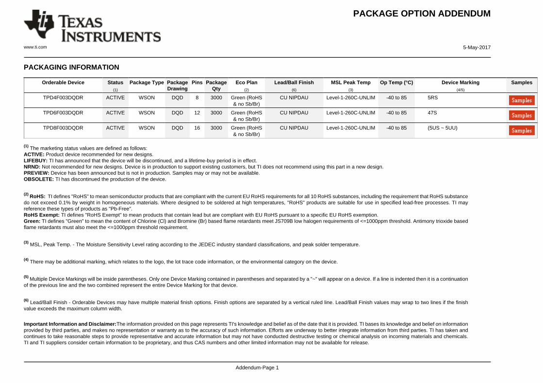
PACKAGING INFORMATION
Orderable Device Status(1)
Package Type PackageDrawing
Pins PackageQty
Eco Plan(2)
Lead/Ball Finish(6)
MSL Peak Temp(3)
Op Temp (°C) Device Marking(4/5)
Samples
TPD4F003DQDR ACTIVE WSON DQD 8 3000 Green (RoHS& no Sb/Br)
CU NIPDAU Level-1-260C-UNLIM -40 to 85 5RS
TPD6F003DQDR ACTIVE WSON DQD 12 3000 Green (RoHS& no Sb/Br)
CU NIPDAU Level-1-260C-UNLIM -40 to 85 47S
TPD8F003DQDR ACTIVE WSON DQD 16 3000 Green (RoHS& no Sb/Br)
CU NIPDAU Level-1-260C-UNLIM -40 to 85 (5US ~ 5UU)
(1) The marketing status values are defined as follows:ACTIVE: Product device recommended for new designs.LIFEBUY: TI has announced that the device will be discontinued, and a lifetime-buy period is in effect.NRND: Not recommended for new designs. Device is in production to support existing customers, but TI does not recommend using this part in a new design.PREVIEW: Device has been announced but is not in production. Samples may or may not be available.OBSOLETE: TI has discontinued the production of the device.
(2) RoHS: TI defines "RoHS" to mean semiconductor products that are compliant with the current EU RoHS requirements for all 10 RoHS substances, including the requirement that RoHS substancedo not exceed 0.1% by weight in homogeneous materials. Where designed to be soldered at high temperatures, "RoHS" products are suitable for use in specified lead-free processes. TI mayreference these types of products as "Pb-Free".RoHS Exempt: TI defines "RoHS Exempt" to mean products that contain lead but are compliant with EU RoHS pursuant to a specific EU RoHS exemption.Green: TI defines "Green" to mean the content of Chlorine (Cl) and Bromine (Br) based flame retardants meet JS709B low halogen requirements of <=1000ppm threshold. Antimony trioxide basedflame retardants must also meet the <=1000ppm threshold requirement.
(3) MSL, Peak Temp. - The Moisture Sensitivity Level rating according to the JEDEC industry standard classifications, and peak solder temperature.
(4) There may be additional marking, which relates to the logo, the lot trace code information, or the environmental category on the device.
(5) Multiple Device Markings will be inside parentheses. Only one Device Marking contained in parentheses and separated by a "~" will appear on a device. If a line is indented then it is a continuationof the previous line and the two combined represent the entire Device Marking for that device.
(6) Lead/Ball Finish - Orderable Devices may have multiple material finish options. Finish options are separated by a vertical ruled line. Lead/Ball Finish values may wrap to two lines if the finishvalue exceeds the maximum column width.
Important Information and Disclaimer:The information provided on this page represents TI's knowledge and belief as of the date that it is provided. TI bases its knowledge and belief on informationprovided by third parties, and makes no representation or warranty as to the accuracy of such information. Efforts are underway to better integrate information from third parties. TI has taken andcontinues to take reasonable steps to provide representative and accurate information but may not have conducted destructive testing or chemical analysis on incoming materials and chemicals.TI and TI suppliers consider certain information to be proprietary, and thus CAS numbers and other limited information may not be available for release.
PACKAGE OPTION ADDENDUM
www.ti.com 5-May-2017
Addendum-Page 2
In no event shall TI's liability arising out of such information exceed the total purchase price of the TI part(s) at issue in this document sold by TI to Customer on an annual basis.
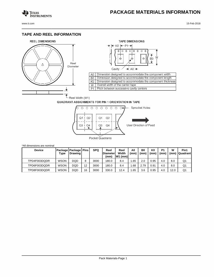
TAPE AND REEL INFORMATION
*All dimensions are nominal
Device PackageType
PackageDrawing
Pins SPQ ReelDiameter
(mm)
ReelWidth
W1 (mm)
A0(mm)
B0(mm)
K0(mm)
P1(mm)
W(mm)
Pin1Quadrant
TPD4F003DQDR WSON DQD 8 3000 180.0 8.4 1.65 2.0 0.95 4.0 8.0 Q1
TPD6F003DQDR WSON DQD 12 3000 180.0 8.4 1.68 2.79 0.91 4.0 8.0 Q1
TPD8F003DQDR WSON DQD 16 3000 330.0 12.4 1.65 3.6 0.95 4.0 12.0 Q1
PACKAGE MATERIALS INFORMATION
www.ti.com 15-Feb-2018
Pack Materials-Page 1
*All dimensions are nominal
Device Package Type Package Drawing Pins SPQ Length (mm) Width (mm) Height (mm)
TPD4F003DQDR WSON DQD 8 3000 183.0 183.0 20.0
TPD6F003DQDR WSON DQD 12 3000 183.0 183.0 20.0
TPD8F003DQDR WSON DQD 16 3000 358.0 335.0 35.0
PACKAGE MATERIALS INFORMATION
www.ti.com 15-Feb-2018
Pack Materials-Page 2

IMPORTANT NOTICE
Texas Instruments Incorporated (TI) reserves the right to make corrections, enhancements, improvements and other changes to itssemiconductor products and services per JESD46, latest issue, and to discontinue any product or service per JESD48, latest issue. Buyersshould obtain the latest relevant information before placing orders and should verify that such information is current and complete.TI’s published terms of sale for semiconductor products (http://www.ti.com/sc/docs/stdterms.htm) apply to the sale of packaged integratedcircuit products that TI has qualified and released to market. Additional terms may apply to the use or sale of other types of TI products andservices.Reproduction of significant portions of TI information in TI data sheets is permissible only if reproduction is without alteration and isaccompanied by all associated warranties, conditions, limitations, and notices. TI is not responsible or liable for such reproduceddocumentation. Information of third parties may be subject to additional restrictions. Resale of TI products or services with statementsdifferent from or beyond the parameters stated by TI for that product or service voids all express and any implied warranties for theassociated TI product or service and is an unfair and deceptive business practice. TI is not responsible or liable for any such statements.Buyers and others who are developing systems that incorporate TI products (collectively, “Designers”) understand and agree that Designersremain responsible for using their independent analysis, evaluation and judgment in designing their applications and that Designers havefull and exclusive responsibility to assure the safety of Designers' applications and compliance of their applications (and of all TI productsused in or for Designers’ applications) with all applicable regulations, laws and other applicable requirements. Designer represents that, withrespect to their applications, Designer has all the necessary expertise to create and implement safeguards that (1) anticipate dangerousconsequences of failures, (2) monitor failures and their consequences, and (3) lessen the likelihood of failures that might cause harm andtake appropriate actions. Designer agrees that prior to using or distributing any applications that include TI products, Designer willthoroughly test such applications and the functionality of such TI products as used in such applications.TI’s provision of technical, application or other design advice, quality characterization, reliability data or other services or information,including, but not limited to, reference designs and materials relating to evaluation modules, (collectively, “TI Resources”) are intended toassist designers who are developing applications that incorporate TI products; by downloading, accessing or using TI Resources in anyway, Designer (individually or, if Designer is acting on behalf of a company, Designer’s company) agrees to use any particular TI Resourcesolely for this purpose and subject to the terms of this Notice.TI’s provision of TI Resources does not expand or otherwise alter TI’s applicable published warranties or warranty disclaimers for TIproducts, and no additional obligations or liabilities arise from TI providing such TI Resources. TI reserves the right to make corrections,enhancements, improvements and other changes to its TI Resources. TI has not conducted any testing other than that specificallydescribed in the published documentation for a particular TI Resource.Designer is authorized to use, copy and modify any individual TI Resource only in connection with the development of applications thatinclude the TI product(s) identified in such TI Resource. NO OTHER LICENSE, EXPRESS OR IMPLIED, BY ESTOPPEL OR OTHERWISETO ANY OTHER TI INTELLECTUAL PROPERTY RIGHT, AND NO LICENSE TO ANY TECHNOLOGY OR INTELLECTUAL PROPERTYRIGHT OF TI OR ANY THIRD PARTY IS GRANTED HEREIN, including but not limited to any patent right, copyright, mask work right, orother intellectual property right relating to any combination, machine, or process in which TI products or services are used. Informationregarding or referencing third-party products or services does not constitute a license to use such products or services, or a warranty orendorsement thereof. Use of TI Resources may require a license from a third party under the patents or other intellectual property of thethird party, or a license from TI under the patents or other intellectual property of TI.TI RESOURCES ARE PROVIDED “AS IS” AND WITH ALL FAULTS. TI DISCLAIMS ALL OTHER WARRANTIES ORREPRESENTATIONS, EXPRESS OR IMPLIED, REGARDING RESOURCES OR USE THEREOF, INCLUDING BUT NOT LIMITED TOACCURACY OR COMPLETENESS, TITLE, ANY EPIDEMIC FAILURE WARRANTY AND ANY IMPLIED WARRANTIES OFMERCHANTABILITY, FITNESS FOR A PARTICULAR PURPOSE, AND NON-INFRINGEMENT OF ANY THIRD PARTY INTELLECTUALPROPERTY RIGHTS. TI SHALL NOT BE LIABLE FOR AND SHALL NOT DEFEND OR INDEMNIFY DESIGNER AGAINST ANY CLAIM,INCLUDING BUT NOT LIMITED TO ANY INFRINGEMENT CLAIM THAT RELATES TO OR IS BASED ON ANY COMBINATION OFPRODUCTS EVEN IF DESCRIBED IN TI RESOURCES OR OTHERWISE. IN NO EVENT SHALL TI BE LIABLE FOR ANY ACTUAL,DIRECT, SPECIAL, COLLATERAL, INDIRECT, PUNITIVE, INCIDENTAL, CONSEQUENTIAL OR EXEMPLARY DAMAGES INCONNECTION WITH OR ARISING OUT OF TI RESOURCES OR USE THEREOF, AND REGARDLESS OF WHETHER TI HAS BEENADVISED OF THE POSSIBILITY OF SUCH DAMAGES.Unless TI has explicitly designated an individual product as meeting the requirements of a particular industry standard (e.g., ISO/TS 16949and ISO 26262), TI is not responsible for any failure to meet such industry standard requirements.Where TI specifically promotes products as facilitating functional safety or as compliant with industry functional safety standards, suchproducts are intended to help enable customers to design and create their own applications that meet applicable functional safety standardsand requirements. Using products in an application does not by itself establish any safety features in the application. Designers mustensure compliance with safety-related requirements and standards applicable to their applications. Designer may not use any TI products inlife-critical medical equipment unless authorized officers of the parties have executed a special contract specifically governing such use.Life-critical medical equipment is medical equipment where failure of such equipment would cause serious bodily injury or death (e.g., lifesupport, pacemakers, defibrillators, heart pumps, neurostimulators, and implantables). Such equipment includes, without limitation, allmedical devices identified by the U.S. Food and Drug Administration as Class III devices and equivalent classifications outside the U.S.TI may expressly designate certain products as completing a particular qualification (e.g., Q100, Military Grade, or Enhanced Product).Designers agree that it has the necessary expertise to select the product with the appropriate qualification designation for their applicationsand that proper product selection is at Designers’ own risk. Designers are solely responsible for compliance with all legal and regulatoryrequirements in connection with such selection.Designer will fully indemnify TI and its representatives against any damages, costs, losses, and/or liabilities arising out of Designer’s non-compliance with the terms and provisions of this Notice.
Mailing Address: Texas Instruments, Post Office Box 655303, Dallas, Texas 75265Copyright © 2018, Texas Instruments Incorporated