Thin Film Photovoltaics By Justin Hibbard. What is a thin film photovoltaic? Thin film voltaics are...
9
Thin Film Photovoltaics By Justin Hibbard
-
date post
22-Dec-2015 -
Category
Documents
-
view
220 -
download
0
Transcript of Thin Film Photovoltaics By Justin Hibbard. What is a thin film photovoltaic? Thin film voltaics are...
Thin Film Photovoltaics
By Justin Hibbard
• What is a thin film photovoltaic?• Thin film voltaics are materials that have a light
absorbing thickness that is less than 10 μm.• The thin film material can converting sunlight to
electricity.• Thin films are predicted to be as efficient as
monocrystalline Si wafer cells with more R & D.• Need more R & D to evolve from the laboratory
to the marketplace. • Two competing materials are
(CIGS):Cu(In,Ga)Se2 and CdTe.
Thin Film Photovoltaics
Thin film photovoltaic devices take advantage of absorption of ir-vis-ir light by semiconductors and converts the light to power.
What is a semiconductor?Semiconductors are materials that require a “turn on” energy to conduct energy
≈ current. Semiconductors share the electrons respectively with the individual atomic
nuclei and require a minimum voltage to make the electrons mobile. Whereas metals are materials that are referred to as conductors and have “free” electrons that respond to a small voltage.
Semiconductors are materials that prefer a Lewis/closed shell structure.This rule may be deviated with the addition of element(s) that differ by group
number ±1,0. Which may give the material an extra or a missing (hole) valence electron. This atomic substitution allows the material scientist to “tune” the material by manipulation of the conduction properties of the material.
Semiconductors are preferable because of the ability to tune the eV with the right elemental mixture and the small amount of material needed.
Thin Film Photovoltaics
Thin Film PhotovoltaicsThin films technologies have a common device/module structure: substrate, base electrode, absorber, junction layer, top electrode, patterning steps for monolithic
integration and encapsulation but in a reverse order. Thin film photovoltaics are cheap if the elements are not rare. They are becoming
cheaper to produce and will become cheaper with time be R & D. Monocrystalline Si is expensive to grow. Amorphous and polycrystalline silicon
are not very efficient. Thin film CIGS cell and modules are 19.5% and 13% efficient and CdTe cells and modules are 16.5% and 10.2% efficient. CdTe and
CIGS PV modules have the potential to reach cost effective PV-generated electricity.
They have transitioned from the laboratory to the market place. Pilot production/first-time manufacturing (US) ~ 25 MW. CdTe
technology ramping to 75 MW. Enjoying a flux of venture capital funding.Transitioning from the lab to manufacturing has been much more difficult
than anticipated.
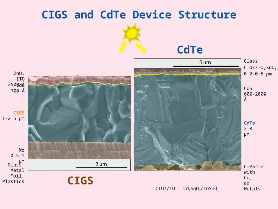
ZnO, ITO2500 Å
CdS700 Å
Mo0.5-1 µm
Glass,Metal Foil,
Plastics
Glass
CTO/ZTO,SnO2
0.2-0.5 µm
CdS600-2000 Å
CdTe2-8 µm
CIGS1-2.5 µm
C-Pastewith Cu,or Metals
CIGS and CdTe Device Structure
CTO/ZTO = Cd2SnO4/ZnSnOx
CIGS
CdTe
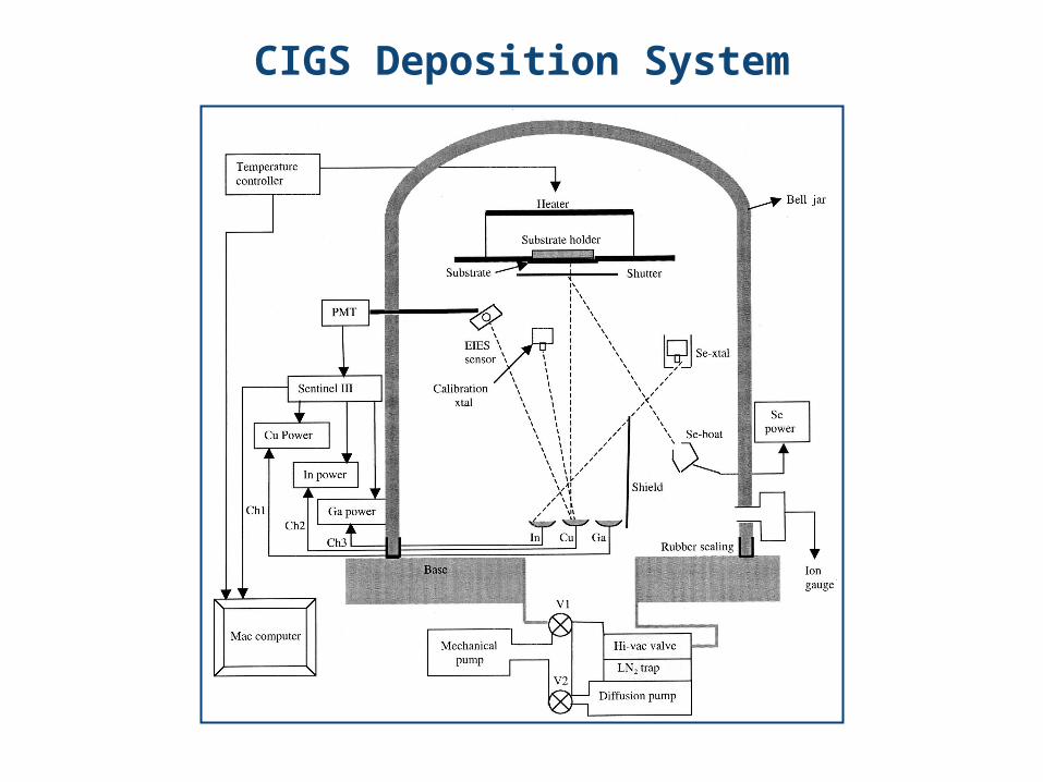
CIGS Deposition System
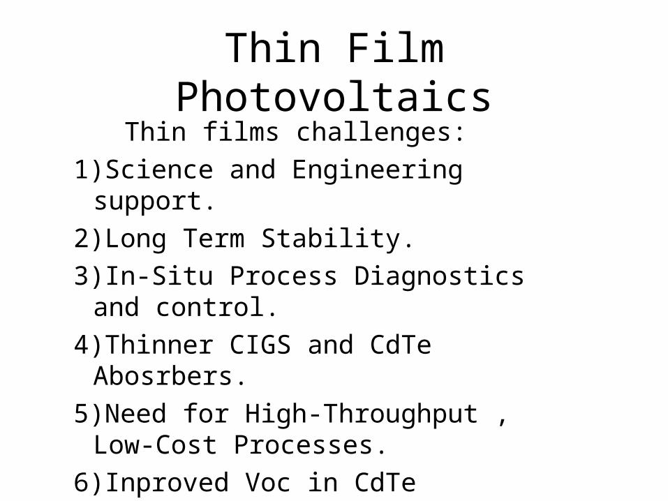
Thin Film PhotovoltaicsThin films challenges:
1)Science and Engineering support.
2)Long Term Stability.
3)In-Situ Process Diagnostics and control.
4)Thinner CIGS and CdTe Abosrbers.
5)Need for High-Throughput , Low-Cost Processes.
6)Inproved Voc in CdTe devices.
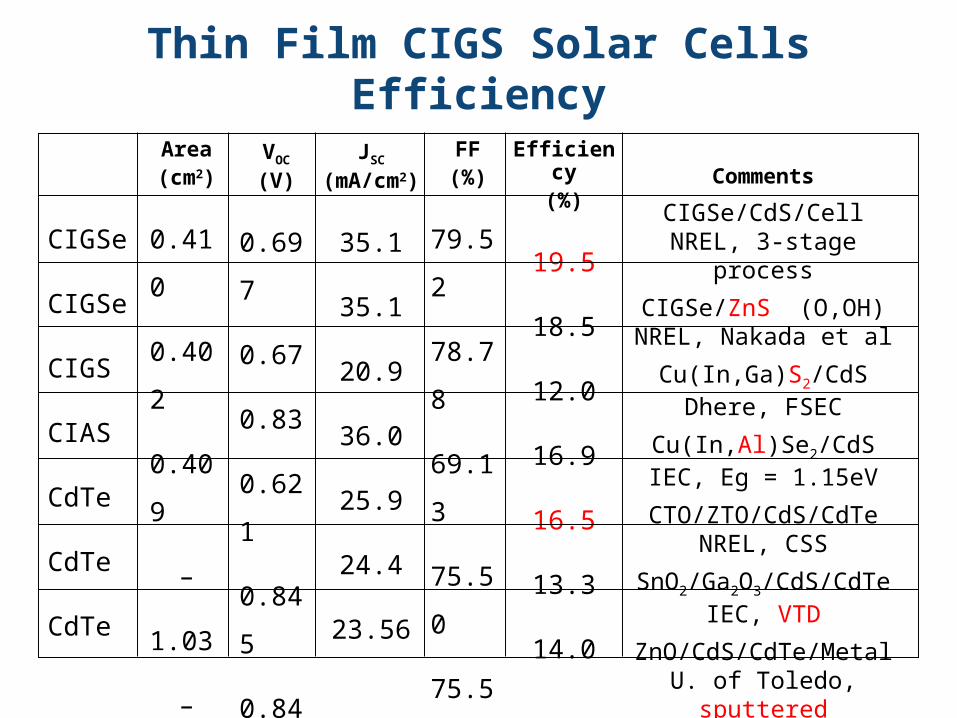
Thin Film CIGS Solar CellsEfficiency
Area(cm2)
CIGSe
CIGSe
CIGS
CIAS
CdTe
CdTe
CdTe
Area(cm2)
0.410
0.402
0.409
–
1.03
–
0.16
VOC
(V)
0.697
0.67
0.83
0.621
0.845
0.840
0.814
JSC
(mA/cm2)
35.1
35.1
20.9
36.0
25.9
24.4
23.56
FF(%)
79.52
78.78
69.13
75.50
75.51
65.00
73.25
Efficiency(%)
19.5
18.5
12.0
16.9
16.5
13.3
14.0
Comments
CIGSe/CdS/CellNREL, 3-stage process
CIGSe/ZnS (O,OH)NREL, Nakada et al
Cu(In,Ga)S2/CdSDhere, FSEC
Cu(In,Al)Se2/CdSIEC, Eg = 1.15eV
CTO/ZTO/CdS/CdTeNREL, CSS
SnO2/Ga2O3/CdS/CdTeIEC, VTD
ZnO/CdS/CdTe/MetalU. of Toledo, sputtered
Thin Film Photovoltaics
Justin Hibbard thanks the nrel.gov webpage for pictures and
information.