theoretical study for photocatalytic hydrogen evolution ... · Back-illuminated Si photocathode: a...
17
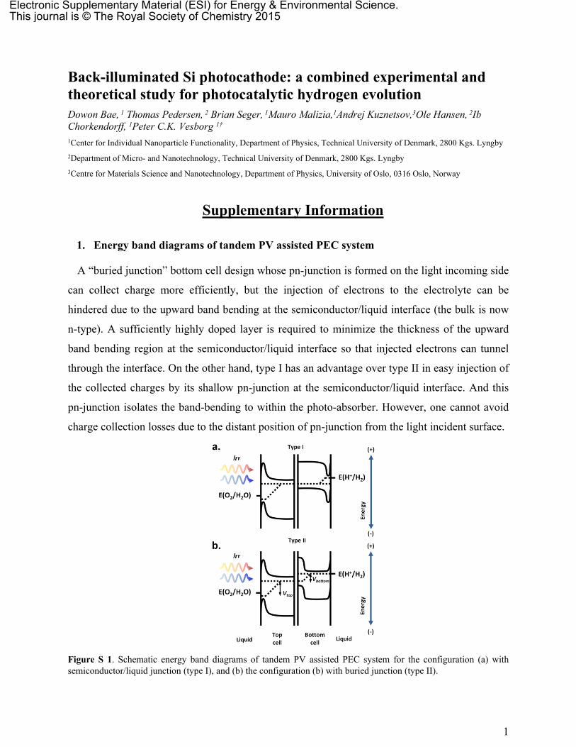
Back-illuminated Si photocathode: a combined experimental and theoretical study for photocatalytic hydrogen evolution Dowon Bae, 1 Thomas Pedersen, 2 Brian Seger, 1 Mauro Malizia, 1 Andrej Kuznetsov, 3 Ole Hansen, 2 Ib Chorkendorff, 1 Peter C.K. Vesborg 1† 1 Center for Individual Nanoparticle Functionality, Department of Physics, Technical University of Denmark, 2800 Kgs. Lyngby 2 Department of Micro- and Nanotechnology, Technical University of Denmark, 2800 Kgs. Lyngby 3 Centre for Materials Science and Nanotechnology, Department of Physics, University of Oslo, 0316 Oslo, Norway Supplementary Information 1. Energy band diagrams of tandem PV assisted PEC system A “buried junction” bottom cell design whose pn-junction is formed on the light incoming side can collect charge more efficiently, but the injection of electrons to the electrolyte can be hindered due to the upward band bending at the semiconductor/liquid interface (the bulk is now n-type). A sufficiently highly doped layer is required to minimize the thickness of the upward band bending region at the semiconductor/liquid interface so that injected electrons can tunnel through the interface. On the other hand, type I has an advantage over type II in easy injection of the collected charges by its shallow pn-junction at the semiconductor/liquid interface. And this pn-junction isolates the band-bending to within the photo-absorber. However, one cannot avoid charge collection losses due to the distant position of pn-junction from the light incident surface. Figure S 1. Schematic energy band diagrams of tandem PV assisted PEC system for the configuration (a) with semiconductor/liquid junction (type I), and (b) the configuration (b) with buried junction (type II). 1 Electronic Supplementary Material (ESI) for Energy & Environmental Science. This journal is © The Royal Society of Chemistry 2015
Transcript of theoretical study for photocatalytic hydrogen evolution ... · Back-illuminated Si photocathode: a...
Back-illuminated Si photocathode: a combined experimental and theoretical study for photocatalytic hydrogen evolution Dowon Bae, 1 Thomas Pedersen, 2 Brian Seger, 1Mauro Malizia,1Andrej Kuznetsov,3Ole Hansen, 2Ib Chorkendorff, 1Peter C.K. Vesborg 1†
1Center for Individual Nanoparticle Functionality, Department of Physics, Technical University of Denmark, 2800 Kgs. Lyngby2Department of Micro- and Nanotechnology, Technical University of Denmark, 2800 Kgs. Lyngby3Centre for Materials Science and Nanotechnology, Department of Physics, University of Oslo, 0316 Oslo, Norway
Supplementary Information
1. Energy band diagrams of tandem PV assisted PEC system
A “buried junction” bottom cell design whose pn-junction is formed on the light incoming side
can collect charge more efficiently, but the injection of electrons to the electrolyte can be
hindered due to the upward band bending at the semiconductor/liquid interface (the bulk is now
n-type). A sufficiently highly doped layer is required to minimize the thickness of the upward
band bending region at the semiconductor/liquid interface so that injected electrons can tunnel
through the interface. On the other hand, type I has an advantage over type II in easy injection of
the collected charges by its shallow pn-junction at the semiconductor/liquid interface. And this
pn-junction isolates the band-bending to within the photo-absorber. However, one cannot avoid
charge collection losses due to the distant position of pn-junction from the light incident surface.
Figure S 1. Schematic energy band diagrams of tandem PV assisted PEC system for the configuration (a) with semiconductor/liquid junction (type I), and (b) the configuration (b) with buried junction (type II).
1
Electronic Supplementary Material (ESI) for Energy & Environmental Science.This journal is © The Royal Society of Chemistry 2015
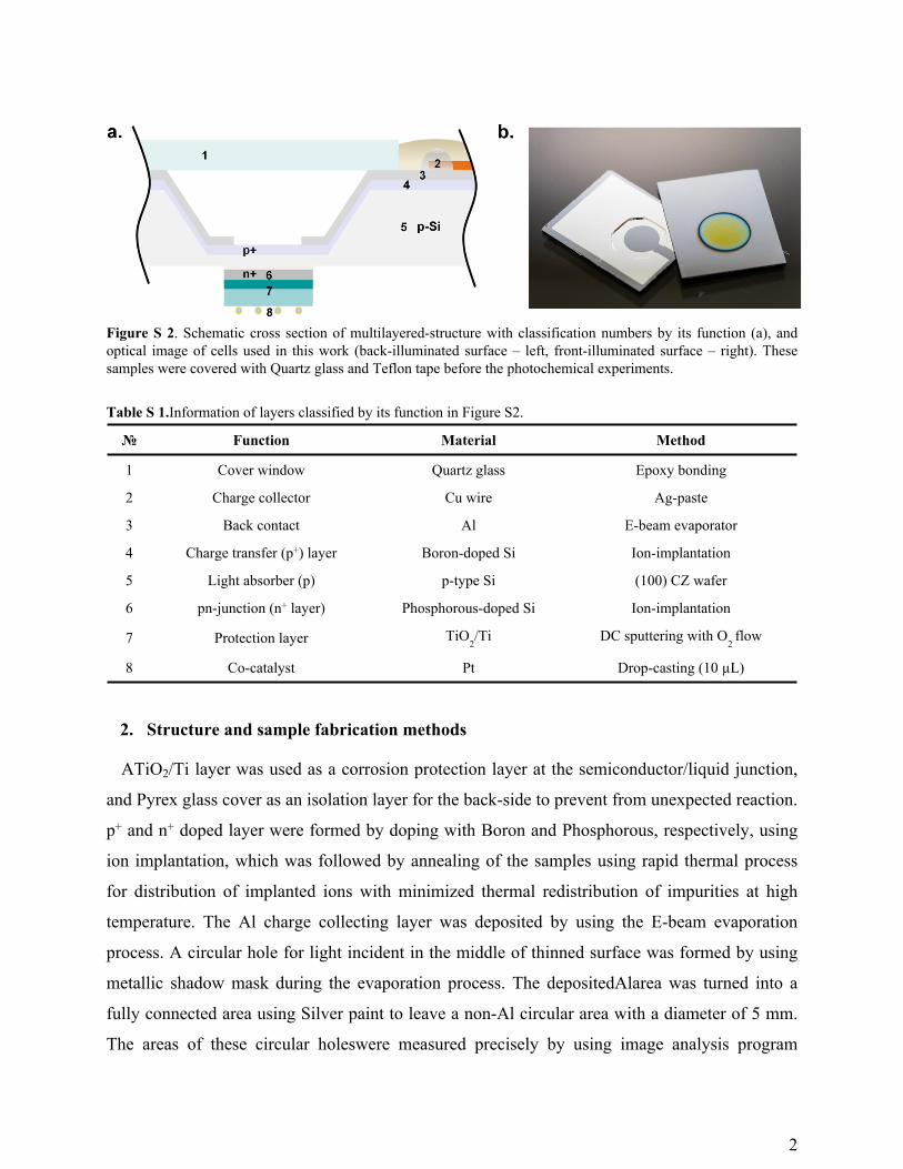
Figure S 2. Schematic cross section of multilayered-structure with classification numbers by its function (a), and optical image of cells used in this work (back-illuminated surface – left, front-illuminated surface – right). These samples were covered with Quartz glass and Teflon tape before the photochemical experiments.
Table S 1.Information of layers classified by its function in Figure S2.
2. Structure and sample fabrication methods
ATiO2/Ti layer was used as a corrosion protection layer at the semiconductor/liquid junction,
and Pyrex glass cover as an isolation layer for the back-side to prevent from unexpected reaction.
p+ and n+ doped layer were formed by doping with Boron and Phosphorous, respectively, using
ion implantation, which was followed by annealing of the samples using rapid thermal process
for distribution of implanted ions with minimized thermal redistribution of impurities at high
temperature. The Al charge collecting layer was deposited by using the E-beam evaporation
process. A circular hole for light incident in the middle of thinned surface was formed by using
metallic shadow mask during the evaporation process. The depositedAlarea was turned into a
fully connected area using Silver paint to leave a non-Al circular area with a diameter of 5 mm.
The areas of these circular holeswere measured precisely by using image analysis program
2
№ Function Material Method
1 Cover window Quartz glass Epoxy bonding
2 Charge collector Cu wire Ag-paste
3 Back contact Al E-beam evaporator
4 Charge transfer (p+) layer Boron-doped Si Ion-implantation
5 Light absorber (p) p-type Si (100) CZ wafer
6 pn-junction (n+ layer) Phosphorous-doped Si Ion-implantation
7 Protection layer TiO2/Ti DC sputtering with O
2 flow
8 Co-catalyst Pt Drop-casting (10 µL)

ImageJ 1.46r. The front surfaces (bottom surface in Figure S2a) were covered by hole punched
(Ø 5 mm) Teflon tape, and these holes were also measured precisely using the image analysis
program. The Pt was drop-casted as a last step onto the opened TiO2 surface.The detailed
information of layers classified by its function can be found in Table S1.
3. Calculation for band diagram
3.1. Calculation at pn+-junction
Most of this band diagram has already been demonstrated in our previous works1. In
explaining the band diagram, we will start from the pn-junction of electrode and move towards
the electrolyte. The p-Si wafer has a band gap (Eg) of 1.124 eV, an acceptor density (NA) of
3·1015 cm-3. The bulk p-Si valence band (VB) can be determined as a function of working
potential (E):
𝐸𝑉, 𝑝 ‒ 𝑆𝑖 = 𝐸 ‒𝑘𝑇𝑒
𝑙𝑛(𝑁𝐴,𝑝 ‒ 𝑆𝑖
𝑁𝑉, 𝑆𝑖)
In figure S3the working potential corresponds to the hole quasi-Fermi level. k is Boltzmann’s
constant, T is temperature (298 K), e is the elementary charge, and NV, Si is the density of states in
the valence band, which is 1.8·1019 cm-3 for Si2. Assuming the pinning of the band edges of the
semiconductor at the interface (0 V vs. RHE) the EV, p-Siis 0.22 V.
The Surface of the p-Si was doped with phosphorous by ion implantation process and n+ emitter
layer was formed at the surface. The process simulation program (Athena, SILVACO) was used
to determine the donor density (ND), which is approximately 5·1019 cm-3. The bulk valence band
of the n+ Si can be determined via equation:
𝐸𝐶, 𝑛 ‒ 𝑆𝑖 = 𝐸 +𝑘𝑇𝑒
𝑙𝑛(𝑁𝐷,𝑛 ‒ 𝑆𝑖
𝑁𝐶, 𝑆𝑖)
where NC stands for the density of states in the conduction band, which is 2.8·1019 cm-3 for Si2.
Under the same assumption as above the EC,n-Si is 0.015 V.
At the pn+-junction a built-in potential will be formed which can be determined in the dark via
equation:
𝑉𝑏𝑖 =𝑘𝑇𝑒
𝐿𝑛(𝑁𝐷,𝑛 ‒ 𝑆𝑖 ∙ 𝑁𝐴,𝑝 ‒ 𝑆𝑖
𝑛2𝑖
)
3
where ni is intrinsic carrier density of Si, which is approximately 1.5·1010 cm-3 at room
temperature, and Vbi was found to be 0.9 V. Under illumination Vbiat open circuit voltage
conditions will simply be the Vbi in the dark minus the photo voltage (Vph):
𝑉𝑏𝑖, 𝑂𝐶𝑉 = 𝑉𝑏𝑖 ‒ 𝑉𝑝ℎ
If it is assumed that there are no interfacial losses at the pn+-junction, the Vbias is distributed
between the p-Si and n+-Si as followed:
𝑉𝑏𝑖, 𝑝 ‒ 𝑆𝑖 = 𝑉𝑏𝑖,𝑂𝐶𝑉
𝑁𝐷,𝑛 ‒ 𝑆𝑖
𝑁𝐴,𝑝 ‒ 𝑆𝑖 + 𝑁𝐷,𝑛 ‒ 𝑆𝑖
𝑉𝑏𝑖,𝑛 ‒ 𝑆𝑖 = 𝑉𝑏𝑖,𝑂𝐶𝑉
𝑁𝐴,𝑝 ‒ 𝑆𝑖
𝑁𝐴,𝑝 ‒ 𝑆𝑖 + 𝑁𝐷,𝑛 ‒ 𝑆𝑖
Using above equations, the Vbi,p-Si is 0.43 V and Vbi,n-Si is 1.3·10-5 V.
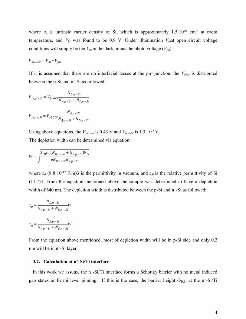
The depletion width can be determined via equation:
𝑊 =2𝜀0𝜀𝑆𝑖(𝑁𝐷,𝑛 ‒ 𝑆𝑖 + 𝑁𝐴,𝑝 ‒ 𝑆𝑖)𝑉𝑏𝑖
𝑒𝑁𝐷,𝑛 ‒ 𝑆𝑖𝑁𝐴,𝑝 ‒ 𝑆𝑖
where ε0 (8.8·10-12 F/m)3 is the permittivity in vacuum, and εSi is the relative permittivity of Si
(11.7)4. From the equation mentioned above the sample was determined to have a depletion
width of 640 nm. The depletion width is distributed between the p-Si and n+-Si as followed:
𝑥𝑝 =𝑁𝐷,𝑛 ‒ 𝑆𝑖
𝑁𝐴,𝑝 ‒ 𝑆𝑖 + 𝑁𝐷,𝑛 ‒ 𝑆𝑖𝑊
𝑥𝑛 =𝑁𝐴,𝑝 ‒ 𝑆𝑖
𝑁𝐴,𝑝 ‒ 𝑆𝑖 + 𝑁𝐷,𝑛 ‒ 𝑆𝑖𝑊
From the equation above mentioned, most of depletion width will be in p-Si side and only 0.2
nm will be in n+-Si layer.
3.2. Calculation at n+-Si/Ti interface
In this work we assume the n+-Si/Ti interface forms a Schottky barrier with no metal induced
gap states or Fermi level pinning. If this is the case, the barrier height ΦB,Si at the n+-Si/Ti
4
interface is the difference between the Ti work function (ΦTi = 4.33 V)5 and the n+-Si ionization
energy (Φn+-Si) plus the deviation between the flat band potential and the conduction band.
Assuming that Φn+-Si is close to the electron affinity of Si (χSi = 4.15 V)6This is shown in
equation below:
𝐵,𝑆𝑖 =𝑇𝑖 ‒𝑆𝑖 +𝑘𝑇𝑒
𝑙𝑛( 𝑁𝐶,𝑆𝑖
𝑁𝐷,𝑛 ‒ 𝑆𝑖)
ΦB,Si was found to be 0.15 V. Since Ti is a metallic layer, and has a high carrier density
compared to the Si, thus the bias will be distributed entirely over the n+ Si region. The band
bending distance in the n+-Si can be determined by equation:
𝑊𝑛 + 𝑆𝑖/𝑇𝑖
=2𝜀𝑆𝑖𝜀0Φ𝐵
𝑒𝑁𝐷,𝑛 ‒ 𝑆𝑖
The barrier width was found to be approximately 1.4 nm, and electron transfer from the Si to the
Ti would most probably have to occur through tunneling.
3.3. Calculation at TiO2/liquid interface
From the Mott-Schottky analysis the TiO2 conduction band was determined to be -0.09 V vs.
RHE, the donor density was 4.5·1019 cm-3, and the flat band potential was -0.07 V vs. RHE.
Since the EFB, TiO2 is very close to the work function of Ti, thus it can be assumed this junction
will show Ohmic behavior. From our previous works we have seen that TiO2-Pt system forms an
Ohmic contact, thus there shouldn’t be a barrier at the interface1.
The depletion region width of TiO2 at the interface is given by:
𝑊𝑇𝑖𝑂2/𝑙𝑖𝑞𝑢𝑖𝑑 =2𝜀𝑜𝜀𝑇𝑖𝑂2Φ𝐵,𝑇𝑖𝑂2
𝑒𝑁𝐷,𝑇𝑖𝑂2
εTiO2 is the relative permittivity of TiO2 (75)7, ND,TiO2is the doping density of TiO2 obtained from
Mott-Shottky analysis (4.5·1019 cm-3). 𝛷B,TiO2 is the barrier height at TiO2/liquid interface, and it
can be simply calculated by:
Φ𝐵,𝑇𝑖𝑂2= 𝐸
𝐻2/𝐻2‒ 𝐸𝐹𝐵,𝑇𝑖𝑂2
+𝑘𝑇𝑒
𝑙𝑛(𝑁𝐷,𝑇𝑖𝑂2
𝑁𝐶,𝑇𝑖𝑂2)
5
where NC,TiO2 is the density of states in the conduction band, which is 6.8·1020 cm-3 for TiO28.
Since we assume that interface forms Fermi level pinning, above-mentioned equation results in
ΦB,TiO2 of 0.038 V. Applying this values results in WTiO2/liquid of 1.02 nm.
3.4. Calculation at p+p-junction
The shallow doped p+-Si VB can be determined through the flat band:
𝐸𝑉, 𝑝 + ‒ 𝑆𝑖
= 𝐸 ‒𝑘𝑇𝑒
𝑙𝑛(𝑁𝐴,𝑝 + ‒ 𝑆𝑖
𝑁𝑉, 𝑆𝑖 )Using acceptor density values of p+ Si NA,p+-Si (1·1020 cm-3), the valence band of p+ layer is 0.04
V. There are no simple expressions predicting the depletion width, but the width is on the order
of a Debye length:
𝐿𝐷 =𝜀0𝜀𝑆𝑖𝑘𝑇
𝑒2𝑁𝐴,𝑝 ‒ 𝑆𝑖
Considering all values used above, the depletion width is approximately 75 nm.
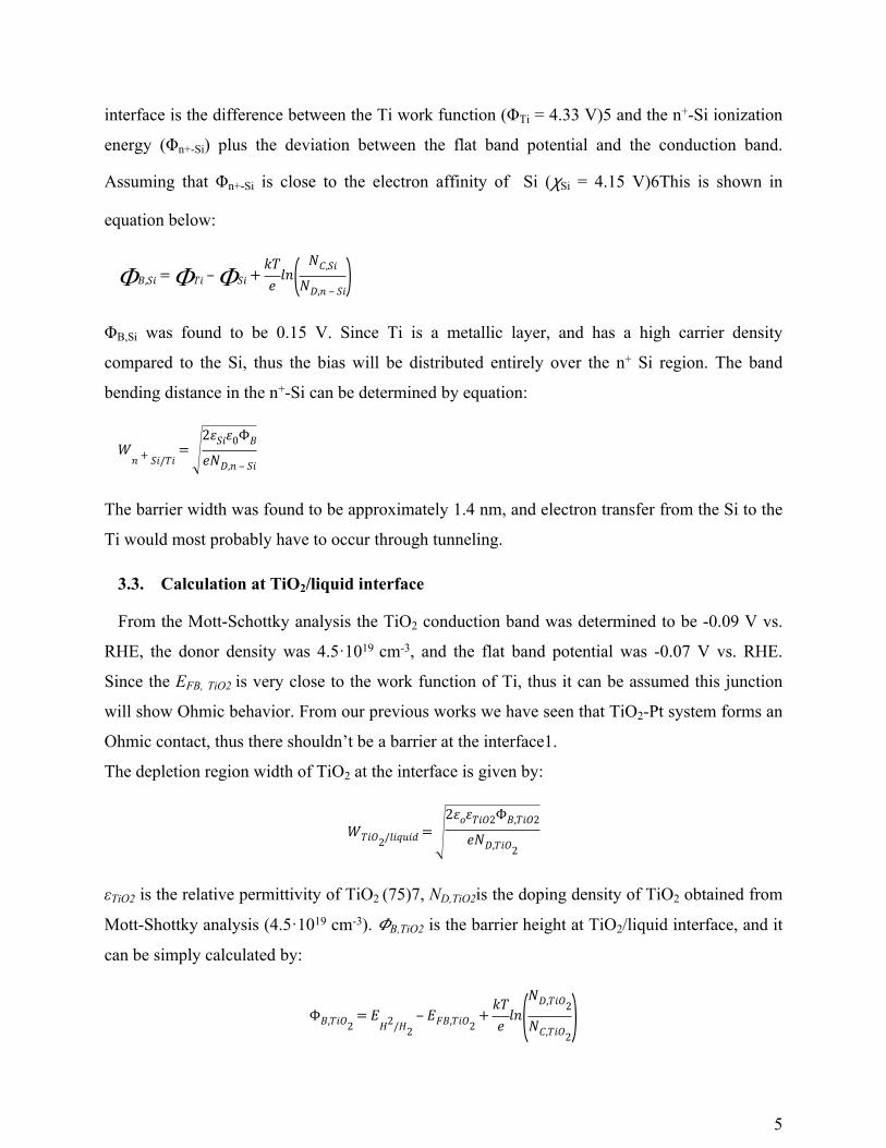
Figure S 3.Schematic energy diagram of the pn+ Si with Ti-TiO2 surface in the dark in equilibrium with the H+/H2 reaction (a), and illuminated condition with photovoltage (b).
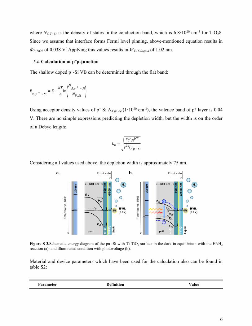
Material and device parameters which have been used for the calculation also can be found in table S2:
6
Parameter Definition Value
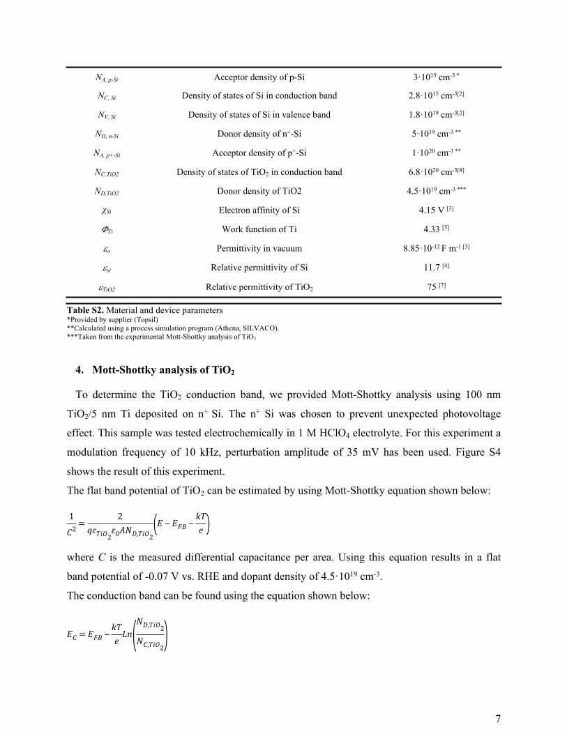
Table S2. Material and device parameters*Provided by supplier (Topsil)**Calculated using a process simulation program (Athena, SILVACO).***Taken from the experimental Mott-Shottky analysis of TiO2
4. Mott-Shottky analysis of TiO2
To determine the TiO2 conduction band, we provided Mott-Shottky analysis using 100 nm
TiO2/5 nm Ti deposited on n+ Si. The n+ Si was chosen to prevent unexpected photovoltage
effect. This sample was tested electrochemically in 1 M HClO4 electrolyte. For this experiment a
modulation frequency of 10 kHz, perturbation amplitude of 35 mV has been used. Figure S4
shows the result of this experiment.
The flat band potential of TiO2 can be estimated by using Mott-Shottky equation shown below:
1
𝐶2=
2𝑞𝜀𝑇𝑖𝑂2
𝜀0𝐴𝑁𝐷,𝑇𝑖𝑂2(𝐸 ‒ 𝐸𝐹𝐵 ‒
𝑘𝑇𝑒 )
where C is the measured differential capacitance per area. Using this equation results in a flat
band potential of -0.07 V vs. RHE and dopant density of 4.5·1019 cm-3.
The conduction band can be found using the equation shown below:
𝐸𝐶 = 𝐸𝐹𝐵 ‒𝑘𝑇𝑒
𝐿𝑛(𝑁𝐷,𝑇𝑖𝑂2
𝑁𝐶,𝑇𝑖𝑂2)
7
NA, p-Si Acceptor density of p-Si 3·1015 cm-3 *
NC, Si Density of states of Si in conduction band 2.8·1015 cm-3[2]
NV, Si Density of states of Si in valence band 1.8·1019 cm-3[2]
ND, n-Si Donor density of n+-Si 5·1019 cm-3 **
NA, p+-Si Acceptor density of p+-Si 1·1020 cm-3 **
NC,TiO2 Density of states of TiO2 in conduction band 6.8·1020 cm-3[8]
ND,TiO2 Donor density of TiO2 4.5·1019 cm-3 ***
χSi Electron affinity of Si 4.15 V [3]
𝛷Ti Work function of Ti 4.33 [5]
o Permittivity in vacuum 8.85·10-12 F m-1 [3]
si Relative permittivity of Si 11.7 [4]
TiO2 Relative permittivity of TiO2 75 [7]
The equation results in a conduction band at -0.09 V vs. RHE.
Figure S 4.Mott-Schottky plot of sputtered 100 nm TiO2/5 nm Ti on n+ Si surface.
5. Role of p+ layer
Some samples were fabricated without p+ doped layer to demonstrate the importance of having
a p+ sheet-conducting layer. The schematic cross sections of these samples can be found in
Figure S5. All layers are fabricated using same process as mentioned in table S1. Figure S6
shows the cyclic voltammogram (CV) for photocatalytic H2 evolution of the pn+-Si electrodes
with direct back contact at the middle of the sample and back contact on Al charge collector
under front side illumination. H2 could be visually observed bubbling off from the
semiconductor/liquid interface as the current increased, and it was confirmed by GC
measurement that hydrogen is produced with high Faradaic efficiency (Figure S9 in SI†). Both
samples have open circuit voltage (Voc) well in excess the H+/H2 redox potential (0 V vs. RHE).
8
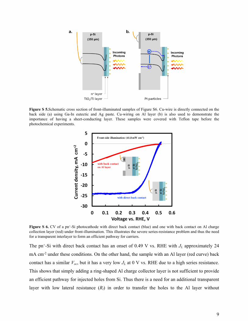
Figure S 5.Schematic cross section of front-illuminated samples of Figure S6. Cu-wire is directly connected on the back side (a) using Ga-In eutectic and Ag paste. Cu-wiring on Al layer (b) is also used to demonstrate the importance of having a sheet-conducting layer. These samples were covered with Teflon tape before the photochemical experiments.
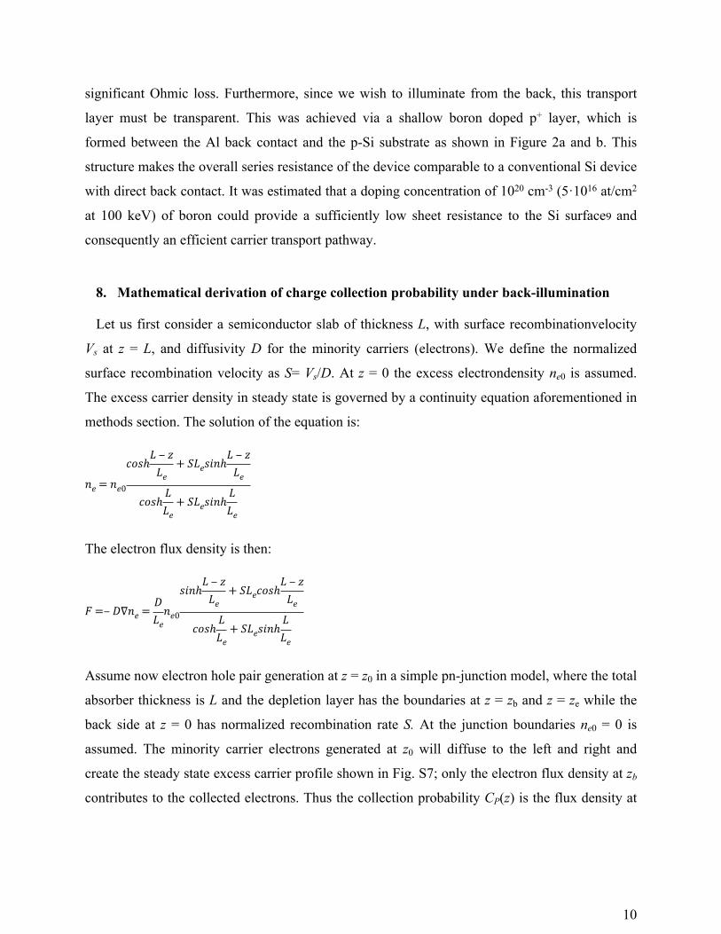
Figure S 6. CV of a pn+-Si photocathode with direct back contact (blue) and one with back contact on Al charge collection layer (red) under front-illumination. This illustrates the severe series-resistance problem and thus the need for a transparent interlayer to form an efficient pathway for carriers.
The pn+-Si with direct back contact has an onset of 0.49 V vs. RHE with JL approximately 24
mA cm-2 under these conditions. On the other hand, the sample with an Al layer (red curve) back
contact has a similar Voc, but it has a very low JL at 0 V vs. RHE due to a high series resistance.
This shows that simply adding a ring-shaped Al charge collector layer is not sufficient to provide
an efficient pathway for injected holes from Si. Thus there is a need for an additional transparent
layer with low lateral resistance (Rl) in order to transfer the holes to the Al layer without
9
significant Ohmic loss. Furthermore, since we wish to illuminate from the back, this transport
layer must be transparent. This was achieved via a shallow boron doped p+ layer, which is
formed between the Al back contact and the p-Si substrate as shown in Figure 2a and b. This
structure makes the overall series resistance of the device comparable to a conventional Si device
with direct back contact. It was estimated that a doping concentration of 1020 cm-3 (5·1016 at/cm2
at 100 keV) of boron could provide a sufficiently low sheet resistance to the Si surface9 and
consequently an efficient carrier transport pathway.
8. Mathematical derivation of charge collection probability under back-illumination
Let us first consider a semiconductor slab of thickness L, with surface recombinationvelocity
Vs at z = L, and diffusivity D for the minority carriers (electrons). We define the normalized
surface recombination velocity as S= Vs/D. At z = 0 the excess electrondensity ne0 is assumed.
The excess carrier density in steady state is governed by a continuity equation aforementioned in
methods section. The solution of the equation is:
𝑛𝑒 = 𝑛𝑒0
𝑐𝑜𝑠ℎ𝐿 ‒ 𝑧
𝐿𝑒+ 𝑆𝐿𝑒𝑠𝑖𝑛ℎ
𝐿 ‒ 𝑧𝐿𝑒
𝑐𝑜𝑠ℎ𝐿𝐿𝑒
+ 𝑆𝐿𝑒𝑠𝑖𝑛ℎ𝐿𝐿𝑒
The electron flux density is then:
𝐹 =‒ 𝐷∇𝑛𝑒 =𝐷𝐿𝑒
𝑛𝑒0
𝑠𝑖𝑛ℎ𝐿 ‒ 𝑧
𝐿𝑒+ 𝑆𝐿𝑒𝑐𝑜𝑠ℎ
𝐿 ‒ 𝑧𝐿𝑒
𝑐𝑜𝑠ℎ𝐿𝐿𝑒
+ 𝑆𝐿𝑒𝑠𝑖𝑛ℎ𝐿𝐿𝑒
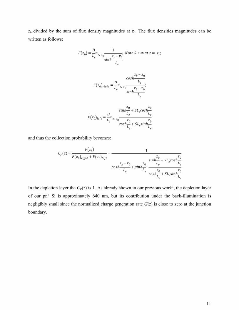
Assume now electron hole pair generation at z = z0 in a simple pn-junction model, where the total
absorber thickness is L and the depletion layer has the boundaries at z = zb and z = ze while the
back side at z = 0 has normalized recombination rate S. At the junction boundaries ne0 = 0 is
assumed. The minority carrier electrons generated at z0 will diffuse to the left and right and
create the steady state excess carrier profile shown in Fig. S7; only the electron flux density at zb
contributes to the collected electrons. Thus the collection probability CP(z) is the flux density at
10
zb divided by the sum of flux density magnitudes at z0. The flux densities magnitudes can be
written as follows:
𝐹(𝑧𝑏) =𝐷𝐿𝑒
𝑛𝑒, 𝑧0
1
𝑠𝑖𝑛ℎ𝑧𝑏 ‒ 𝑧0
𝐿𝑒
, 𝑁𝑜𝑡𝑒 𝑆→ ∞ 𝑎𝑡 𝑧 = 𝑧𝑏;
𝐹(𝑧0)𝑟𝑖𝑔ℎ𝑡 =𝐷𝐿𝑒
𝑛𝑒, 𝑧0
𝑐𝑜𝑠ℎ𝑧𝑏 ‒ 𝑧0
𝐿𝑒
𝑠𝑖𝑛ℎ𝑧𝑏 ‒ 𝑧0
𝐿𝑒
;
𝐹(𝑧0)𝑙𝑒𝑓𝑡 =𝐷𝐿𝑒
𝑛𝑒, 𝑧0
𝑠𝑖𝑛ℎ𝑧0
𝐿𝑒+ 𝑆𝐿𝑒𝑐𝑜𝑠ℎ
𝑧0
𝐿𝑒
𝑐𝑜𝑠ℎ𝑧0
𝐿𝑒+ 𝑆𝐿𝑒𝑠𝑖𝑛ℎ
𝑧0
𝐿𝑒
and thus the collection probability becomes:
𝐶𝑃(𝑧) =𝐹(𝑧𝑏)
𝐹(𝑧0)𝑟𝑖𝑔ℎ𝑡 + 𝐹(𝑧0)𝑙𝑒𝑓𝑡=
1
𝑐𝑜𝑠ℎ𝑧𝑏 ‒ 𝑧0
𝐿𝑒+ 𝑠𝑖𝑛ℎ
𝑧0
𝐿𝑒∙
𝑠𝑖𝑛ℎ𝑧0
𝐿𝑒+ 𝑆𝐿𝑒𝑐𝑜𝑠ℎ
𝑧0
𝐿𝑒
𝑐𝑜𝑠ℎ𝑧0
𝐿𝑒+ 𝑆𝐿𝑒𝑠𝑖𝑛ℎ
𝑧0
𝐿𝑒
In the depletion layer the CP(z) is 1. As already shown in our previous work3, the depletion layer
of our pn+ Si is approximately 640 nm, but its contribution under the back-illumination is
negligibly small since the normalized charge generation rate G(z) is close to zero at the junction
boundary.
11
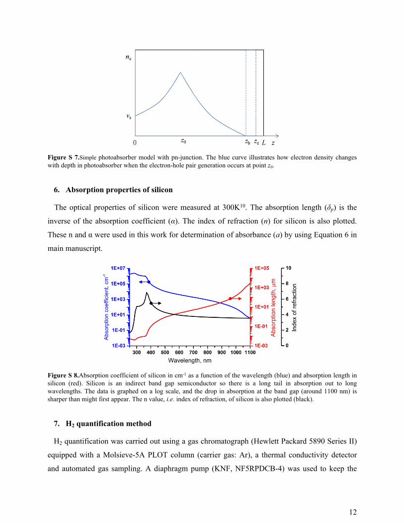
Figure S 7.Simple photoabsorber model with pn-junction. The blue curve illustrates how electron density changes with depth in photoabsorber when the electron-hole pair generation occurs at point z0.
6. Absorption properties of silicon
The optical properties of silicon were measured at 300K10. The absorption length (δp) is the
inverse of the absorption coefficient (α). The index of refraction (n) for silicon is also plotted.
These n and α were used in this work for determination of absorbance (a) by using Equation 6 in
main manuscript.
Figure S 8.Absorption coefficient of silicon in cm-1 as a function of the wavelength (blue) and absorption length in silicon (red). Silicon is an indirect band gap semiconductor so there is a long tail in absorption out to long wavelengths. The data is graphed on a log scale, and the drop in absorption at the band gap (around 1100 nm) is sharper than might first appear. The n value, i.e. index of refraction, of silicon is also plotted (black).
7. H2 quantification method
H2 quantification was carried out using a gas chromatograph (Hewlett Packard 5890 Series II)
equipped with a Molsieve-5A PLOT column (carrier gas: Ar), a thermal conductivity detector
and automated gas sampling. A diaphragm pump (KNF, NF5RPDCB-4) was used to keep the
12
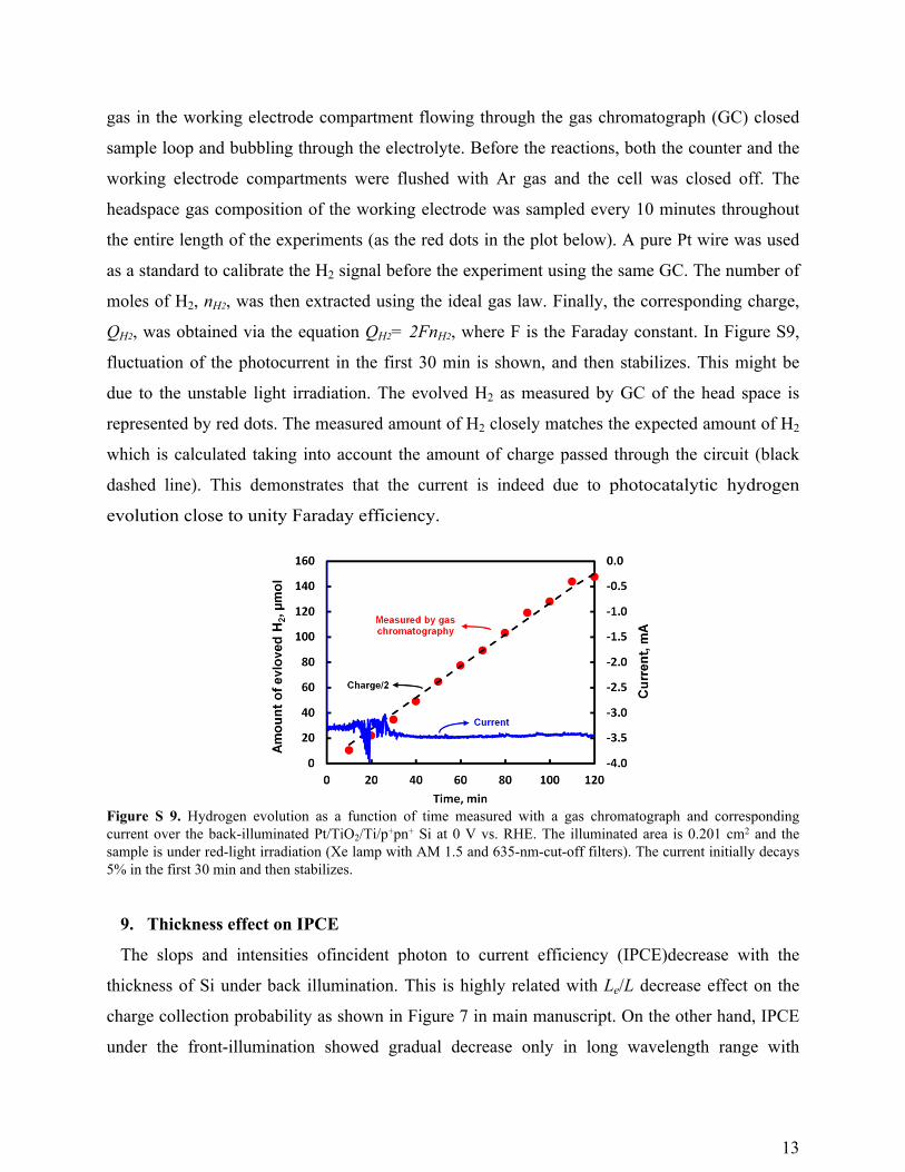
gas in the working electrode compartment flowing through the gas chromatograph (GC) closed
sample loop and bubbling through the electrolyte. Before the reactions, both the counter and the
working electrode compartments were flushed with Ar gas and the cell was closed off. The
headspace gas composition of the working electrode was sampled every 10 minutes throughout
the entire length of the experiments (as the red dots in the plot below). A pure Pt wire was used
as a standard to calibrate the H2 signal before the experiment using the same GC. The number of
moles of H2, nH2, was then extracted using the ideal gas law. Finally, the corresponding charge,
QH2, was obtained via the equation QH2= 2FnH2, where F is the Faraday constant. In Figure S9,
fluctuation of the photocurrent in the first 30 min is shown, and then stabilizes. This might be
due to the unstable light irradiation. The evolved H2 as measured by GC of the head space is
represented by red dots. The measured amount of H2 closely matches the expected amount of H2
which is calculated taking into account the amount of charge passed through the circuit (black
dashed line). This demonstrates that the current is indeed due to photocatalytic hydrogen
evolution close to unity Faraday efficiency.
Figure S 9. Hydrogen evolution as a function of time measured with a gas chromatograph and corresponding current over the back-illuminated Pt/TiO2/Ti/p+pn+ Si at 0 V vs. RHE. The illuminated area is 0.201 cm2 and the sample is under red-light irradiation (Xe lamp with AM 1.5 and 635-nm-cut-off filters). The current initially decays 5% in the first 30 min and then stabilizes.
9. Thickness effect on IPCE
The slops and intensities ofincident photon to current efficiency (IPCE)decrease with the
thickness of Si under back illumination. This is highly related with Le/L decrease effect on the
charge collection probability as shown in Figure 7 in main manuscript. On the other hand, IPCE
under the front-illumination showed gradual decrease only in long wavelength range with
13
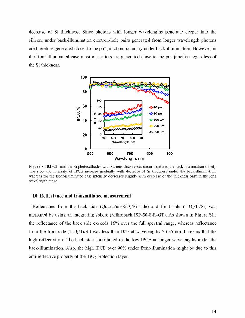
decrease of Si thickness. Since photons with longer wavelengths penetrate deeper into the
silicon, under back-illumination electron-hole pairs generated from longer wavelength photons
are therefore generated closer to the pn+-junction boundary under back-illumination. However, in
the front illuminated case most of carriers are generated close to the pn+-junction regardless of
the Si thickness.
Figure S 10.IPCEfrom the Si photocathodes with various thicknesses under front and the back-illumination (inset). The slop and intensity of IPCE increase gradually with decrease of Si thickness under the back-illumination, whereas for the front-illuminated case intensity decreases slightly with decrease of the thickness only in the long wavelength range.
10. Reflectance and transmittance measurement
Reflectance from the back side (Quartz/air/SiO2/Si side) and front side (TiO2/Ti/Si) was
measured by using an integrating sphere (Mikropack ISP-50-8-R-GT). As shown in Figure S11
the reflectance of the back side exceeds 16% over the full spectral range, whereas reflectance
from the front side (TiO2/Ti/Si) was less than 10% at wavelengths ≥ 635 nm. It seems that the
high reflectivity of the back side contributed to the low IPCE at longer wavelengths under the
back-illumination. Also, the high IPCE over 90% under front-illumination might be due to this
anti-reflective property of the TiO2 protection layer.
14
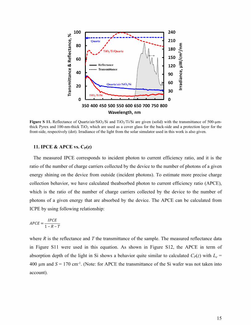
Figure S 11. Reflectance of Quartz/air/SiO2/Si and TiO2/Ti/Si are given (solid) with the transmittance of 500-µm-thick Pyrex and 100-nm-thick TiO2 which are used as a cover glass for the back-side and a protection layer for the front-side, respectively (dot). Irradiance of the light from the solar simulator used in this work is also given.
11. IPCE & APCE vs. CP(z)
The measured IPCE corresponds to incident photon to current efficiency ratio, and it is the
ratio of the number of charge carriers collected by the device to the number of photons of a given
energy shining on the device from outside (incident photons). To estimate more precise charge
collection behavior, we have calculated theabsorbed photon to current efficiency ratio (APCE),
which is the ratio of the number of charge carriers collected by the device to the number of
photons of a given energy that are absorbed by the device. The APCE can be calculated from
ICPE by using following relationship:
𝐴𝑃𝐶𝐸 =𝐼𝑃𝐶𝐸
1 ‒ 𝑅 ‒ 𝑇
where R is the reflectance and T the transmittance of the sample. The measured reflectance data
in Figure S11 were used in this equation. As shown in Figure S12, the APCE in term of
absorption depth of the light in Si shows a behavior quite similar to calculated CP(z) with Le =
400 µm and S = 170 cm-1. (Note: for APCE the transmittance of the Si wafer was not taken into
account).
15
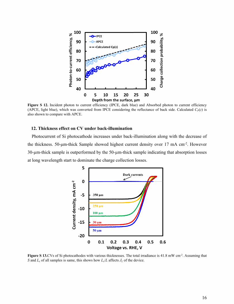
Figure S 12. Incident photon to current efficiency (IPCE, dark blue) and Absorbed photon to current efficiency (APCE, light blue), which was converted from IPCE considering the reflectance of back side. Calculated CP(z) is also shown to compare with APCE.
12. Thickness effect on CV under back-illumination
Photocurrent of Si photocathode increases under back-illumination along with the decrease of
the thickness. 50-μm-thick Sample showed highest current density over 17 mA cm-2. However
30-µm-thick sample is outperformed by the 50-µm-thick sample indicating that absorption losses
at long wavelength start to dominate the charge collection losses.
Figure S 13.CVs of Si photocathodes with various thicknesses. The total irradiance is 41.8 mW cm-2. Assuming that S and Le of all samples is same, this shows how Le/L affects JL of the device.
16
1. B. Seger, T. Pedersen, A. B. Laursen, P. C. K. Vesborg, O. Hansen, I. Chorkendorff, Using TiO2 as a conductive protective layer for photocathodic H2 evolution, J. Am. Chem. Soc., 2013, 135, 1057−1064.
2. L. Vivien, L. Pavesi, Handbook of silicon photonics, Taylor & Francis, Boca Raton, 2013, ch. 1.3., p. 26.3. The NIST reference on constants, units, and uncertainty, http://physics.nist.gov/cgi-bin/cuu/Value?ep0 (accessed Nov. 24, 2014).4. M. –K. Lee, H. –C. Lee, C. –M. Hsu, High dielectric constant titanium oxide grown on amorphous silicon by metal-organic chemical vapour
deposition, Semicond. Sci. Technol., 2006, 21, 604-607.5. H. P. R. Frederikse, CRC Handbook of Chemistry and physics, ed. by D. R. Lide, 78th edition, 1997, pp 12.6. N. Dasgupta, A. Dasgupta, Semiconductor devices: modeling and technology, Prentice-Hall, New Delhi, 2004, ch. 1.3.10., pp. 30.7. D. M. King, X. Du, A. S. Cavanagh, A. Weimer, Confinement in amorphous TiO2 films studied using atomic layer deposition,
Nanotechnology, 2008, 19, 445401-445406.8. J. Bisquert, A. Zaban, M. Greenshtein, I. Mora-Sero, Determination of rate constants for charge transfer and the distribution of
semiconductor and electrolyte electronic energy levels in dye-sensitized solar cells by open-circuit photovoltage decay method, J. Am. Chem. Soc., 2004, 126, 13550-13559.
9. W. R. Thurber, R. L. Mattis, Y. M. Liu, J. J. Filliben, Resistivity-dopant density relationship for boron-doped silicon, J. Electrochem. Soc., 1980, 127, 2291-2294.
10. M. A. Green, M. J. Keevers, Optical properties of intrinsic silicon at 300 K, Prog. Photovoltaics, 1995, 3, 189-192.
17