The Optical Energy Domain - Signals and Systems, Uppsala
28
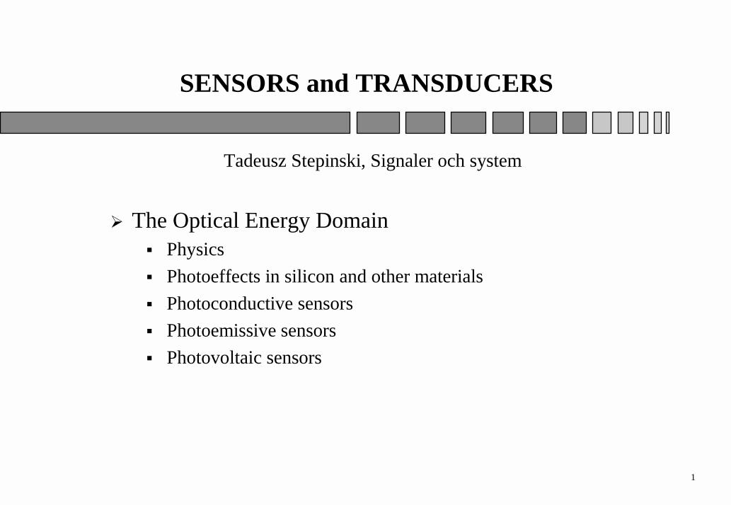
SENSORS and TRANSDUCERS ! The Optical Energy Domain " Physics " Photoeffects in silicon and other materials " Photoconductive sensors " Photoemissive sensors " Photovoltaic sensors Tadeusz Stepinski, Signaler och system 1
Transcript of The Optical Energy Domain - Signals and Systems, Uppsala
SENSORS and TRANSDUCERS
! The Optical Energy Domain" Physics " Photoeffects in silicon and other materials" Photoconductive sensors" Photoemissive sensors" Photovoltaic sensors
Tadeusz Stepinski, Signaler och system
1
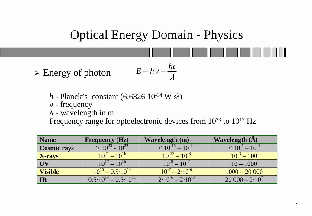
Optical Energy Domain - Physics
! Energy of photon
h - Planck’s constant (6.6326 10-34 W s2)ν - frequencyλ - wavelength in mFrequency range for optoelectronic devices from 1023 to 1012 Hz
2
E = hν = hcλ
Name Frequency (Hz) Wavelength (m) Wavelength (Å) Cosmic rays > 1023 - 1022 < 10-15 – 10-14 < 10-5 – 10-4 X-rays 1021 – 1016 10-13 – 10-8 10-3 – 100 UV 1017 – 1015 10-9 – 10-7 10 – 1000 Visible 1015 – 0.5·1014 10-7 – 2·10-6 1000 – 20 000 IR 0.5·1014 – 0.5·1011 2·10-6 – 2·10-3 20 000 – 2·107
Optical Energy Domain - Physics
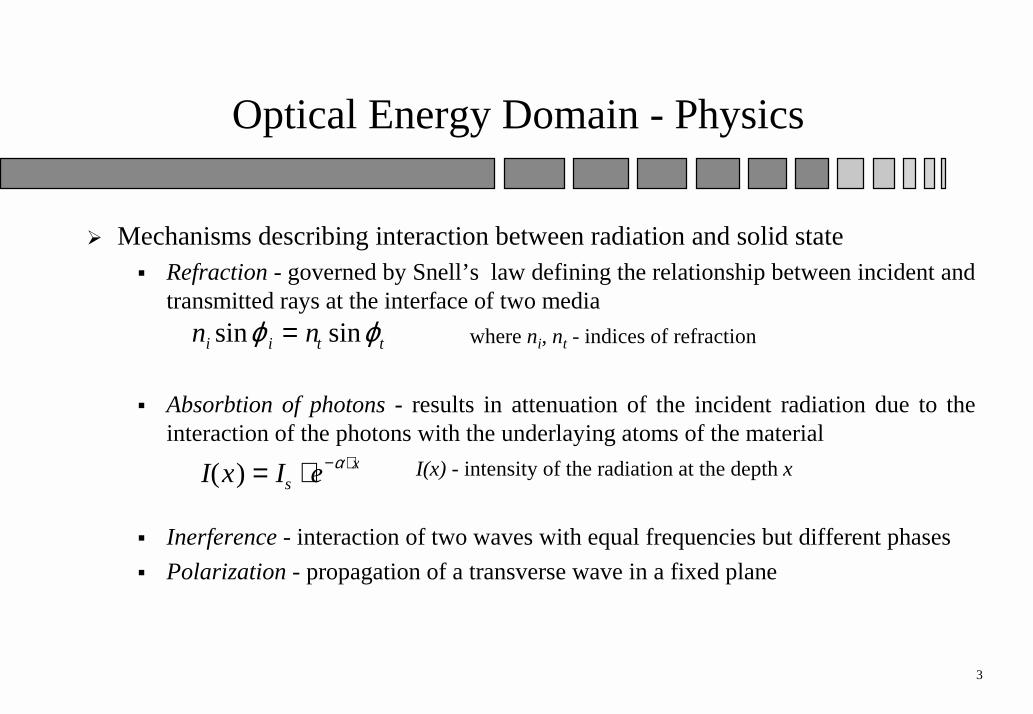
! Mechanisms describing interaction between radiation and solid state" Refraction - governed by Snell’s law defining the relationship between incident and
transmitted rays at the interface of two mediawhere ni, nt - indices of refraction
" Absorbtion of photons - results in attenuation of the incident radiation due to the interaction of the photons with the underlaying atoms of the material
I(x) - intensity of the radiation at the depth x
" Inerference - interaction of two waves with equal frequencies but different phases" Polarization - propagation of a transverse wave in a fixed plane
3
ni sinϕ i = nt sinϕt
I(x) = Is ⋅ e−α ⋅ x
Optical Energy Domain - Physics
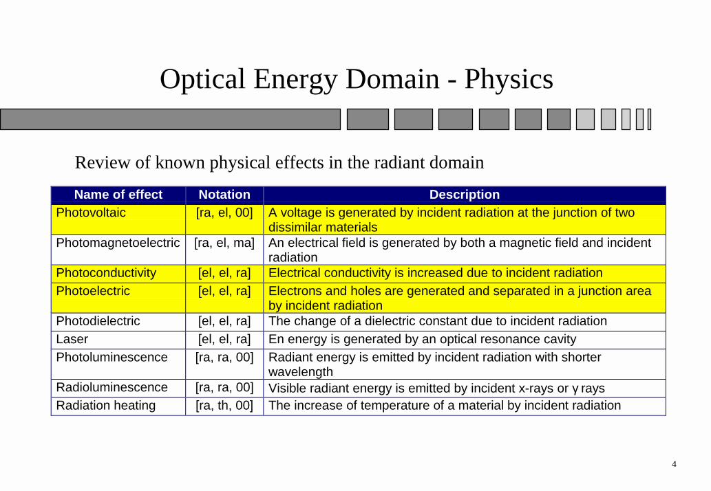
Review of known physical effects in the radiant domain
4
Name of effect Notation DescriptionPhotovoltaic [ra, el, 00] A voltage is generated by incident radiation at the junction of two
dissimilar materialsPhotomagnetoelectric [ra, el, ma] An electrical field is generated by both a magnetic field and incident
radiationPhotoconductivity [el, el, ra] Electrical conductivity is increased due to incident radiationPhotoelectric [el, el, ra] Electrons and holes are generated and separated in a junction area
by incident radiationPhotodielectric [el, el, ra] The change of a dielectric constant due to incident radiationLaser [el, el, ra] En energy is generated by an optical resonance cavityPhotoluminescence [ra, ra, 00] Radiant energy is emitted by incident radiation with shorter
wavelengthRadioluminescence [ra, ra, 00] Visible radiant energy is emitted by incident x-rays or γ raysRadiation heating [ra, th, 00] The increase of temperature of a material by incident radiation
Optical Energy Domain - Physics
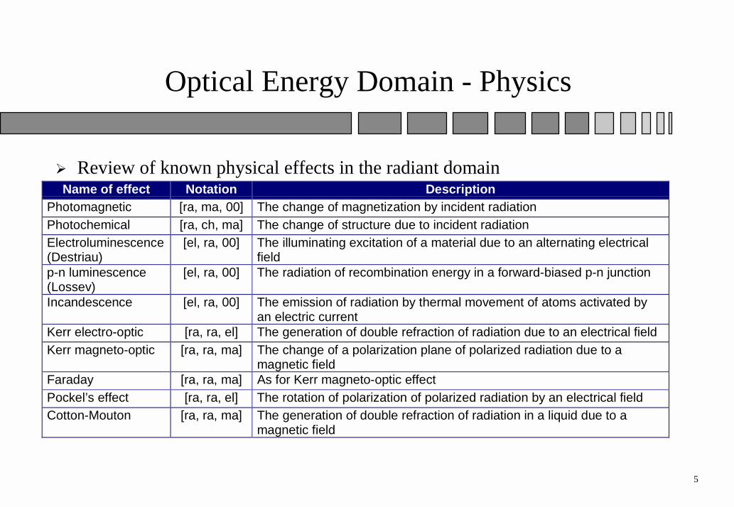
! Review of known physical effects in the radiant domain
5
Name of effect Notation DescriptionPhotomagnetic [ra, ma, 00] The change of magnetization by incident radiationPhotochemical [ra, ch, ma] The change of structure due to incident radiationElectroluminescence(Destriau)
[el, ra, 00] The illuminating excitation of a material due to an alternating electricalfield
p-n luminescence(Lossev)
[el, ra, 00] The radiation of recombination energy in a forward-biased p-n junction
Incandescence [el, ra, 00] The emission of radiation by thermal movement of atoms activated byan electric current
Kerr electro-optic [ra, ra, el] The generation of double refraction of radiation due to an electrical fieldKerr magneto-optic [ra, ra, ma] The change of a polarization plane of polarized radiation due to a
magnetic fieldFaraday [ra, ra, ma] As for Kerr magneto-optic effectPockel’s effect [ra, ra, el] The rotation of polarization of polarized radiation by an electrical fieldCotton-Mouton [ra, ra, ma] The generation of double refraction of radiation in a liquid due to a
magnetic field
Photoconductive sensors
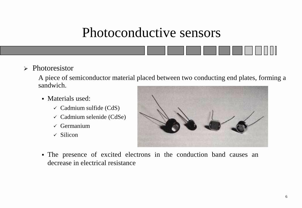
! PhotoresistorA piece of semiconductor material placed between two conducting end plates, forming a sandwich.
6
" Materials used:# Cadmium sulfide (CdS)# Cadmium selenide (CdSe)# Germanium# Silicon
" The presence of excited electrons in the conduction band causes an decrease in electrical resistance
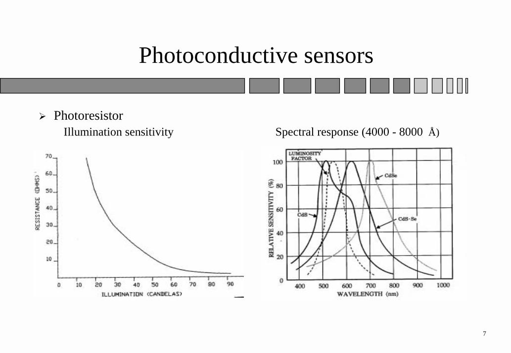
Photoconductive sensors
! PhotoresistorIllumination sensitivity Spectral response (4000 - 8000 Å)
7
Photoconductive sensors
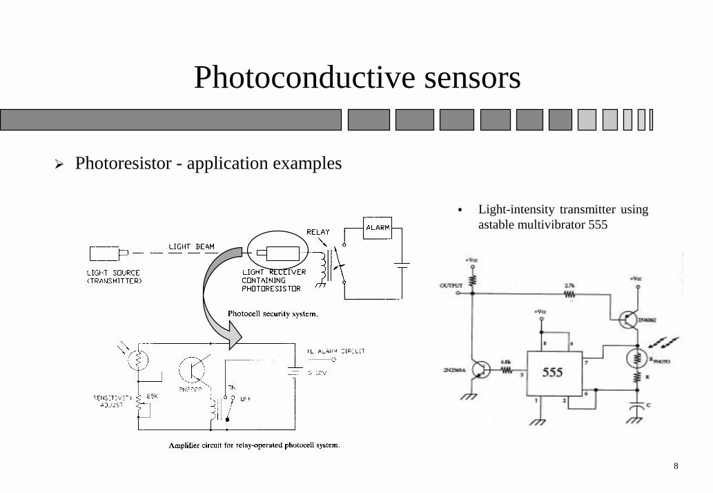
! Photoresistor - application examples
8
" Light-intensity transmitter using astable multivibrator 555
Photoconductive sensors
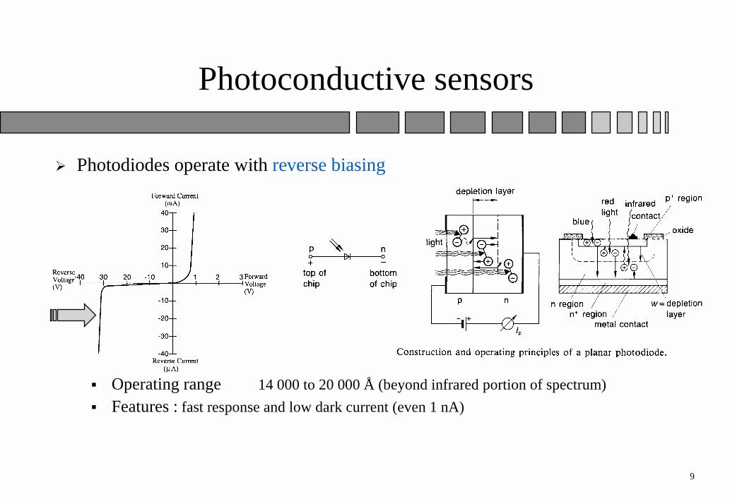
! Photodiodes operate with reverse biasing
" Operating range 14 000 to 20 000 Å (beyond infrared portion of spectrum)" Features : fast response and low dark current (even 1 nA)
9
Photoconductive sensors
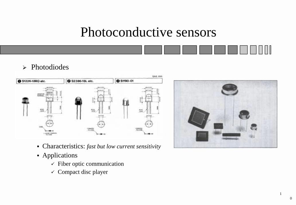
! Photodiodes
" Characteristics: fast but low current sensitivity" Applications
# Fiber optic communication# Compact disc player
10
Photoconductive sensors
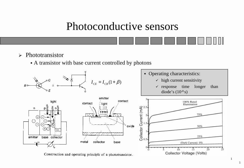
! Phototransistor" A transistor with base current controlled by photons
11
)1( β+= CBCE II
" Operating characteristics:# high current sensitivity# response time longer than
diode’s (10-8 s)
Photoconductive sensors
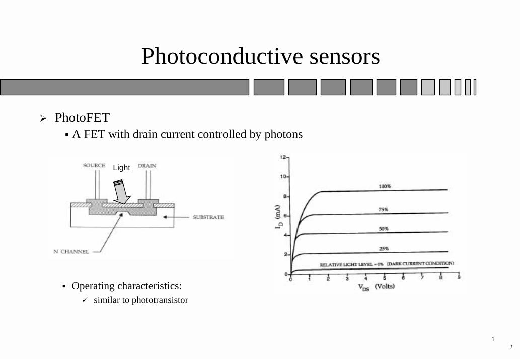
! PhotoFET" A FET with drain current controlled by photons
12
Light
" Operating characteristics:# similar to phototransistor
Photoconductive sensors
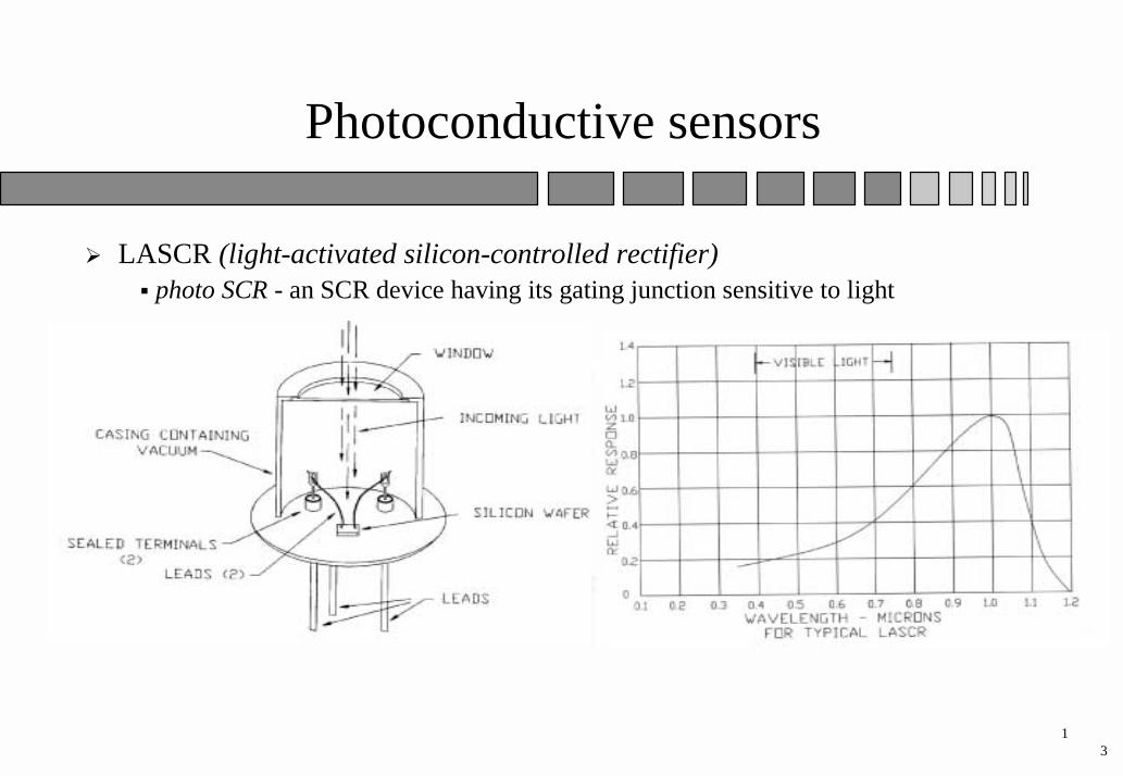
! LASCR (light-activated silicon-controlled rectifier)" photo SCR - an SCR device having its gating junction sensitive to light
13
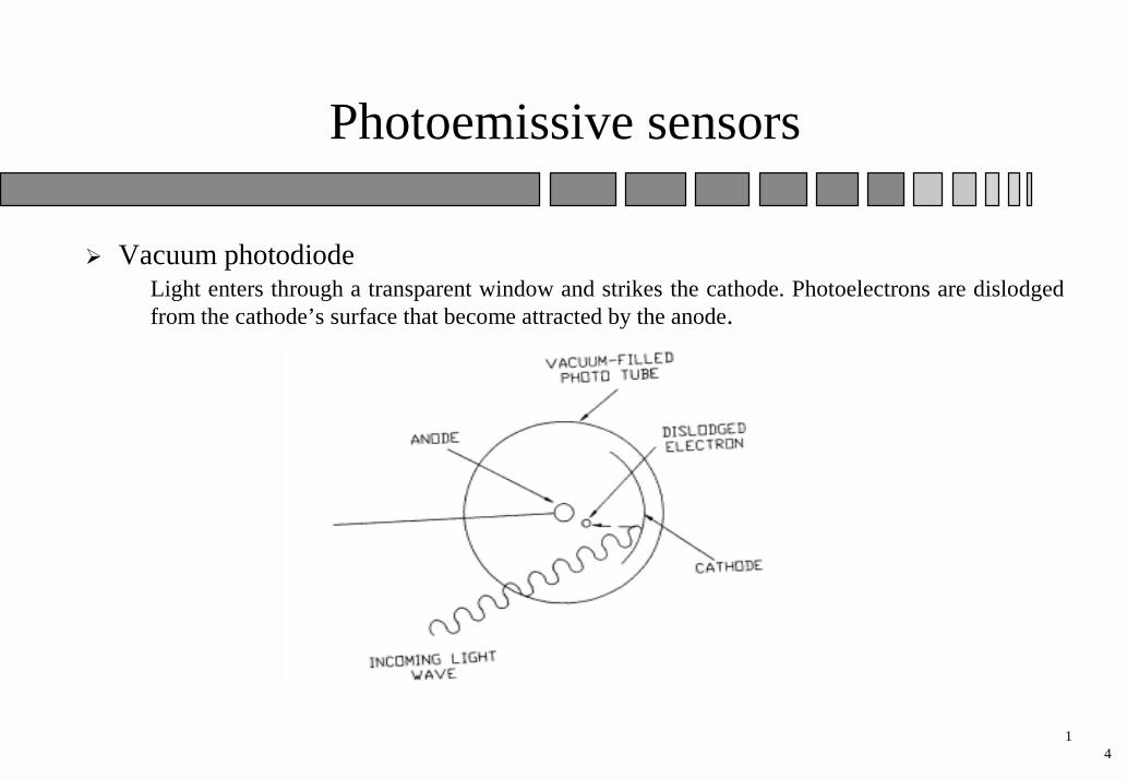
Photoemissive sensors
! Vacuum photodiodeLight enters through a transparent window and strikes the cathode. Photoelectrons are dislodged from the cathode’s surface that become attracted by the anode.
14
Michelson Interferometer
15
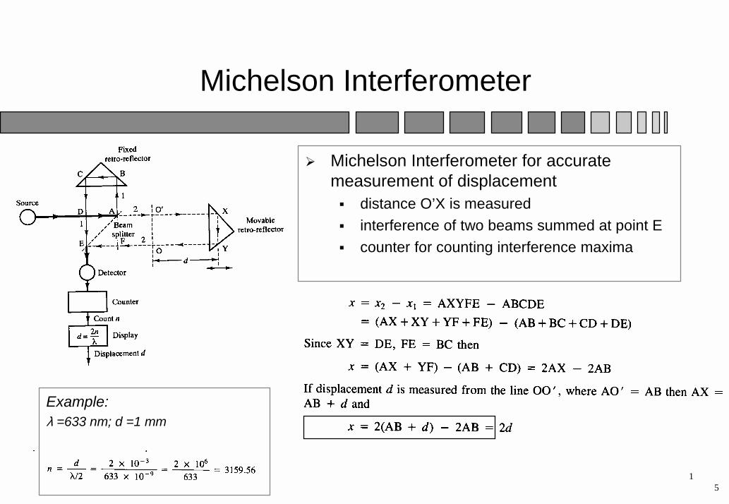
! Michelson Interferometer for accurate measurement of displacement" distance O’X is measured " interference of two beams summed at point E" counter for counting interference maxima
Example:λ =633 nm; d =1 mm
Interferometers
16
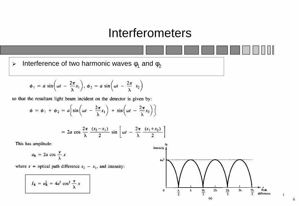
! Interference of two harmonic waves φ1 and φ2
Photoemissive sensors
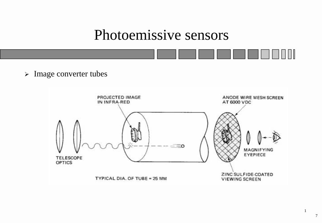
! Image converter tubes
17
Photoemissive sensors
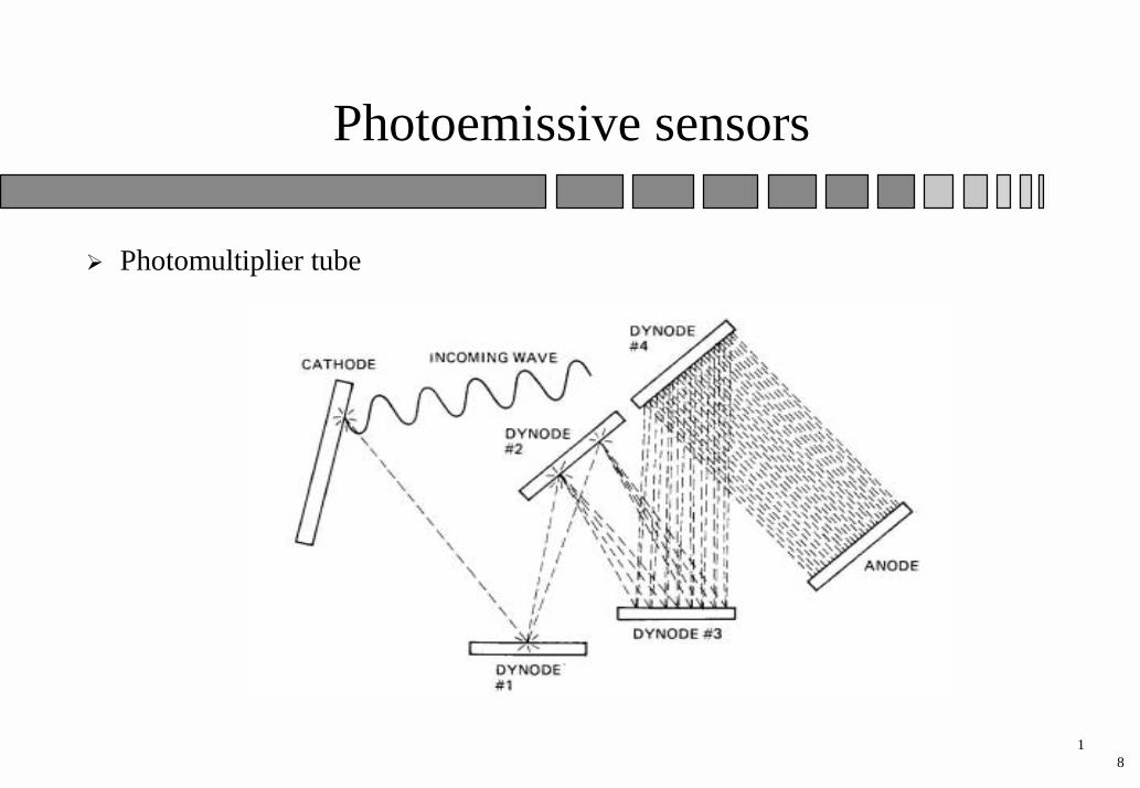
! Photomultiplier tube
18
Photoemissive sensors
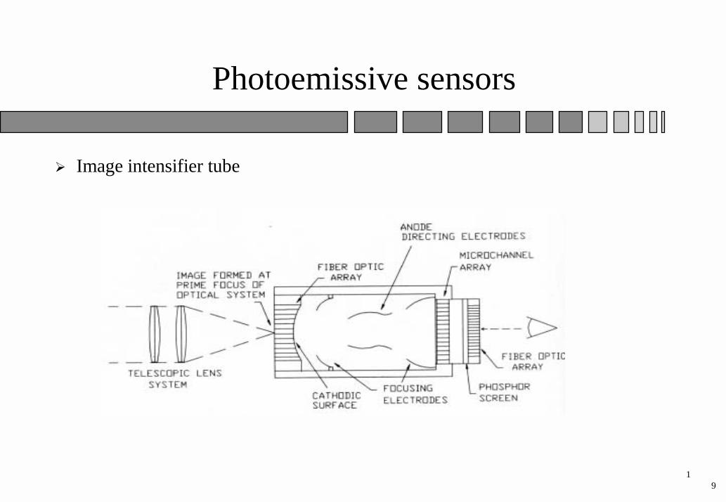
! Image intensifier tube
19
Photoemissive sensors
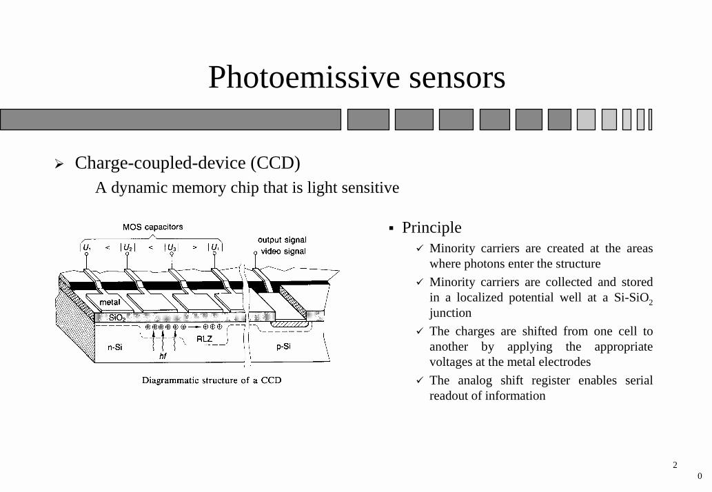
! Charge-coupled-device (CCD)A dynamic memory chip that is light sensitive
20
" Principle# Minority carriers are created at the areas
where photons enter the structure# Minority carriers are collected and stored
in a localized potential well at a Si-SiO2junction
# The charges are shifted from one cell to another by applying the appropriate voltages at the metal electrodes
# The analog shift register enables serial readout of information
Photovoltaic sensors
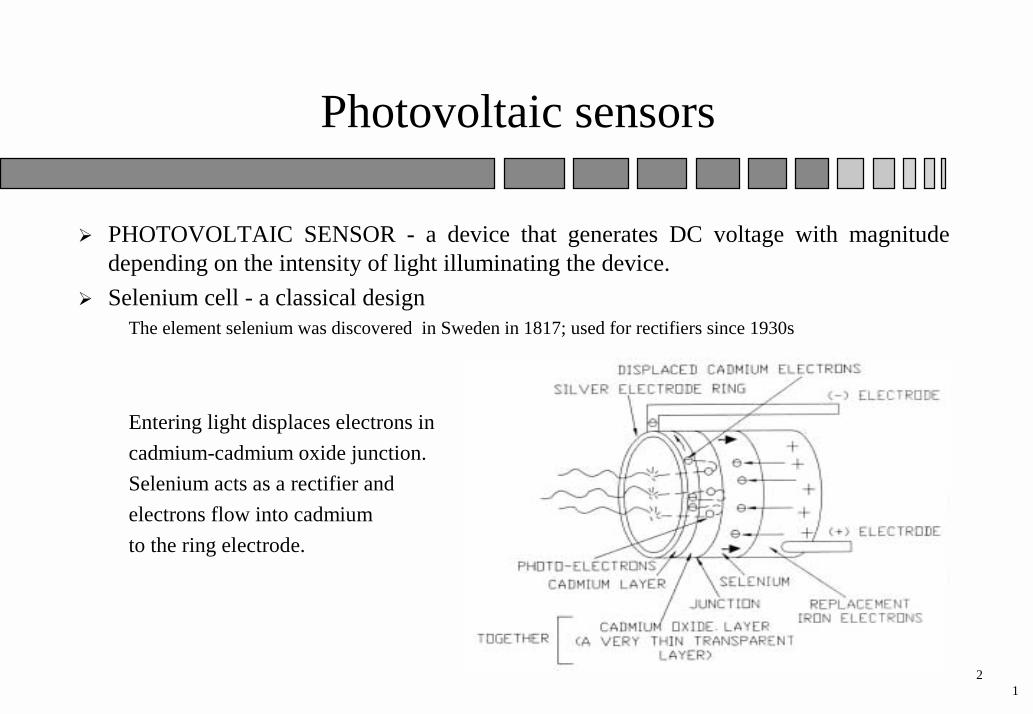
! PHOTOVOLTAIC SENSOR - a device that generates DC voltage with magnitude depending on the intensity of light illuminating the device.
! Selenium cell - a classical designThe element selenium was discovered in Sweden in 1817; used for rectifiers since 1930s
Entering light displaces electrons in cadmium-cadmium oxide junction.Selenium acts as a rectifier and electrons flow into cadmium to the ring electrode.
21
Photovoltaic sensors
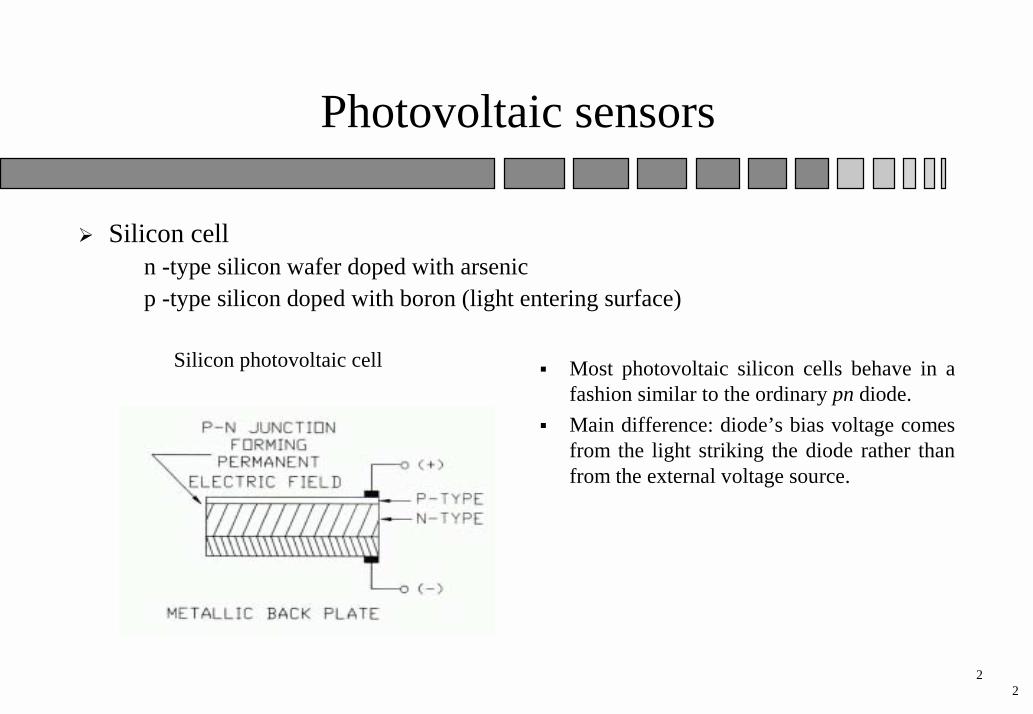
! Silicon celln -type silicon wafer doped with arsenicp -type silicon doped with boron (light entering surface)
Silicon photovoltaic cell
22
" Most photovoltaic silicon cells behave in a fashion similar to the ordinary pn diode.
" Main difference: diode’s bias voltage comes from the light striking the diode rather than from the external voltage source.
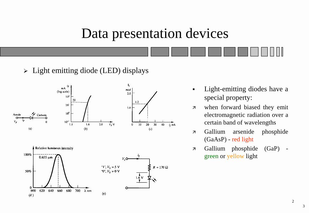
Data presentation devices
! Light emitting diode (LED) displays
23
" Light-emitting diodes have a special property:
$ when forward biased they emit electromagnetic radiation over a certain band of wavelengths
$ Gallium arsenide phosphide (GaAsP) - red light
$ Gallium phosphide (GaP) -green or yellow light
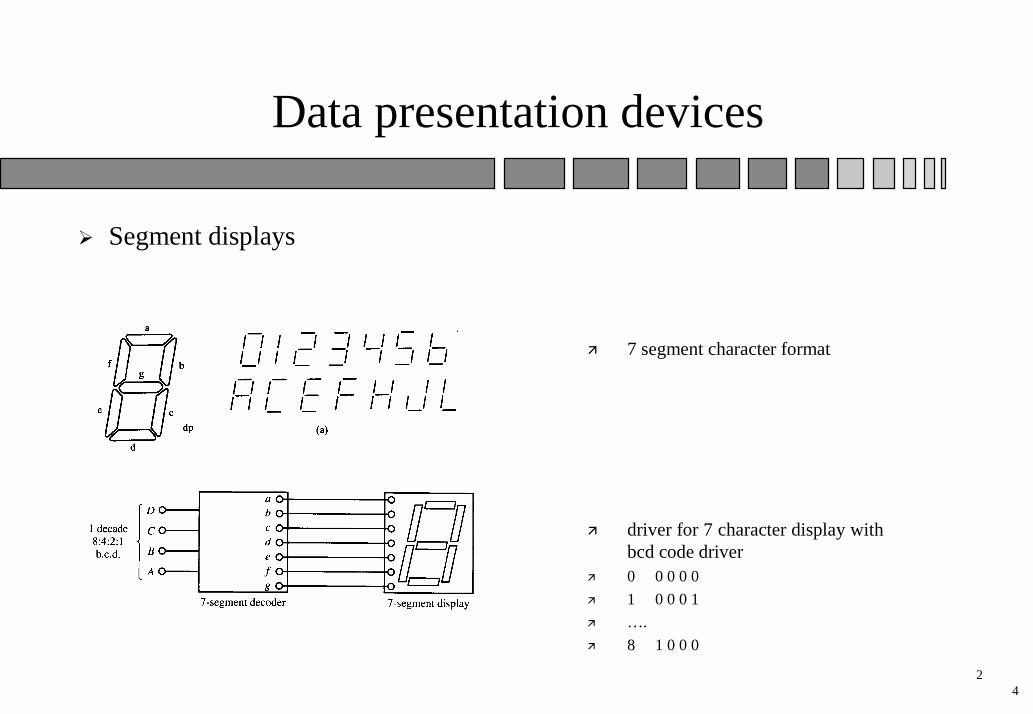
Data presentation devices
! Segment displays
24
$ 7 segment character format
$ driver for 7 character display with bcd code driver
$ 0 0 0 0 0$ 1 0 0 0 1$ ….$ 8 1 0 0 0
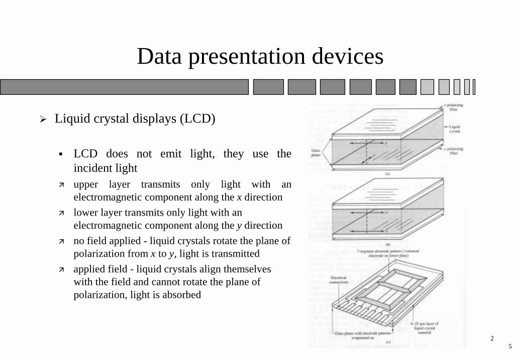
Data presentation devices
! Liquid crystal displays (LCD)
25
" LCD does not emit light, they use the incident light
$ upper layer transmits only light with an electromagnetic component along the x direction
$ lower layer transmits only light with an electromagnetic component along the y direction
$ no field applied - liquid crystals rotate the plane of polarization from x to y, light is transmitted
$ applied field - liquid crystals align themselves with the field and cannot rotate the plane of polarization, light is absorbed
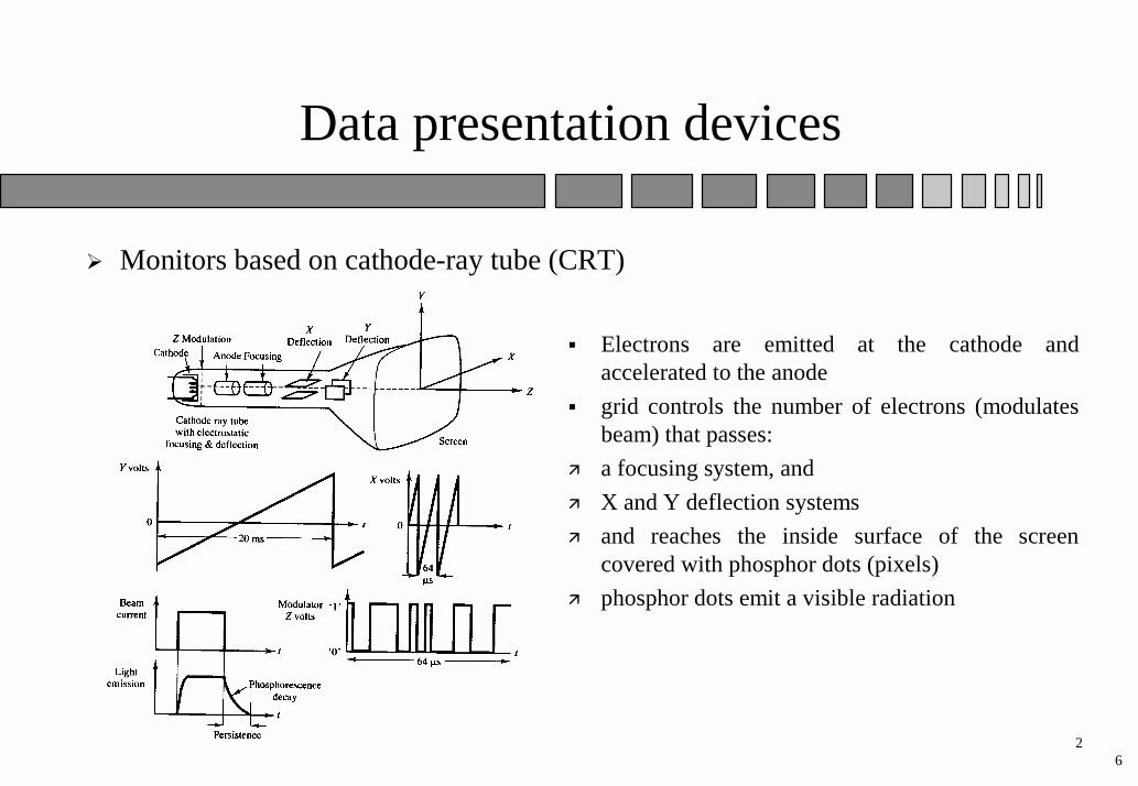
Data presentation devices
! Monitors based on cathode-ray tube (CRT)
26
" Electrons are emitted at the cathode and accelerated to the anode
" grid controls the number of electrons (modulates beam) that passes:
$ a focusing system, and $ X and Y deflection systems $ and reaches the inside surface of the screen
covered with phosphor dots (pixels)$ phosphor dots emit a visible radiation
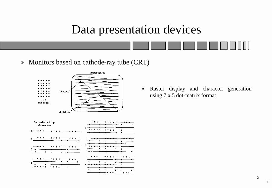
Data presentation devices
! Monitors based on cathode-ray tube (CRT)
27
" Raster display and character generation using 7 x 5 dot-matrix format
Optical Energy Domain - Review questions
" Explain difference between photovoltaic and photoelectric effect, define Miller index for both" Explain function of a photoconductive sensor" Explain the nature of photodiodes dark current" Advantages of phototransistor comparing to photodiode" Operation principle of image converter" What is the purpose of dynode in a photoemission tube " Operation principle of CCD" Operation principle of a photovoltaic sensor (selenium or silicon cell)
28