The Nonlinear Optical Properties of Semiconductors - University of
39
Research Group Optoelectronics GLASGOW UNIVERSITY OF The Nonlinear Optical Properties of Semiconductors David C. Hutchings [email protected] Dept. of Electronics and Electrical Engineering The Nonlinear Optical Properties of Semiconductors – p. 1/39
Transcript of The Nonlinear Optical Properties of Semiconductors - University of
Research GroupOptoelectronics
GLASGOWUNIVERSITY OF
The Nonlinear Optical Properties ofSemiconductors
David C. Hutchings
Dept. of Electronics and Electrical Engineering
The Nonlinear Optical Properties of Semiconductors – p. 1/39
Research GroupOptoelectronics
GLASGOWUNIVERSITY OF
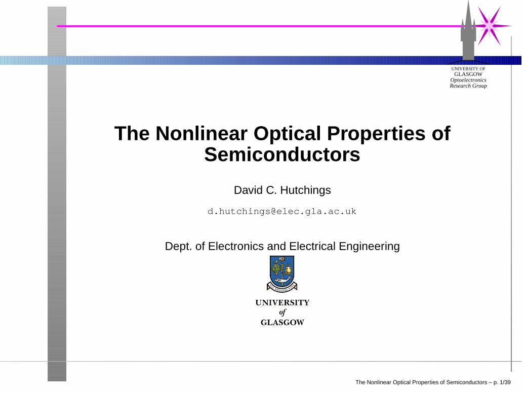
Optical Susceptibility Tensor
P = ε0
[
χ(1)E + χ(2)EE + χ(3)EEE + . . .]
χ(1)ij ω Linear refraction and absorption
χ(2)ijk ω1 + ω2 Sum frequency generation
ω1 − ω2 Difference frequency generation, rectification
ω + 0 Electro-optic (Pockel’s) effect
χ(3)ijkl ω + ω + ω Third harmonic generation
ω − ω + ω Nonlinear refraction and absorption, 4WM
ω + 0 + 0 Kerr electro-optic effect (DC)
The Nonlinear Optical Properties of Semiconductors – p. 2/39
Research GroupOptoelectronics
GLASGOWUNIVERSITY OF
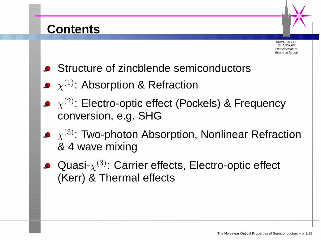
Contents
Structure of zincblende semiconductors
χ(1): Absorption & Refraction
χ(2): Electro-optic effect (Pockels) & Frequencyconversion, e.g. SHG
χ(3): Two-photon Absorption, Nonlinear Refraction& 4 wave mixing
Quasi-χ(3): Carrier effects, Electro-optic effect(Kerr) & Thermal effects
The Nonlinear Optical Properties of Semiconductors – p. 3/39

Research GroupOptoelectronics
GLASGOWUNIVERSITY OF
Waveguide geometry
Slab or rib waveguides
Assume weakly guiding
Also assume nonlinearity weak such thattransverse guided mode unchanged
Conventional orientation with [001] growth and [110]cleavage:
x y
z
The Nonlinear Optical Properties of Semiconductors – p. 4/39

Research GroupOptoelectronics
GLASGOWUNIVERSITY OF
Crystal Symmetries
Common compound semiconductors in photonicshave a zinc-blende (cubic) structure 43m
Note different layer ordering for 111 and 111
Introducing heterostructure, e.g. quantum well,breaks translational invariance in one direction
The Nonlinear Optical Properties of Semiconductors – p. 5/39
Research GroupOptoelectronics
GLASGOWUNIVERSITY OF
Bandstructure models
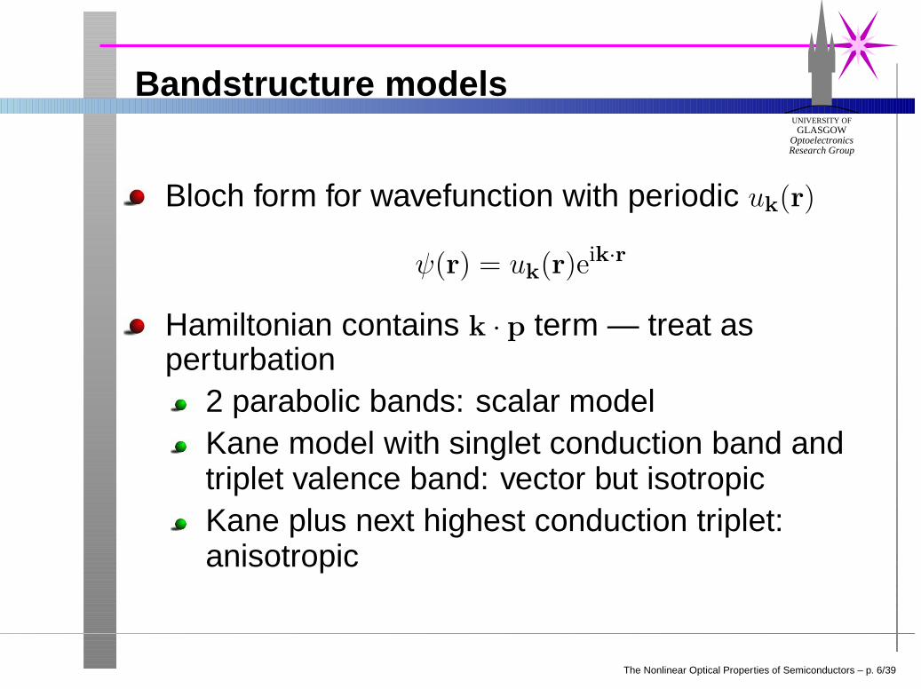
Bloch form for wavefunction with periodic uk(r)
ψ(r) = uk(r)eik·r
Hamiltonian contains k · p term — treat asperturbation
2 parabolic bands: scalar modelKane model with singlet conduction band andtriplet valence band: vector but isotropicKane plus next highest conduction triplet:anisotropic
The Nonlinear Optical Properties of Semiconductors – p. 6/39

Research GroupOptoelectronics
GLASGOWUNIVERSITY OF
AlGaAs bandstructure
AlxGa1−xAs direct bandgap for x < 0.45
The Nonlinear Optical Properties of Semiconductors – p. 7/39

Research GroupOptoelectronics
GLASGOWUNIVERSITY OF
k · p models
∆
∆Γ
Γ
Γ
15
15
1
c
c
v
1
0
E
E
v
c
cE’
The Nonlinear Optical Properties of Semiconductors – p. 8/39
Research GroupOptoelectronics
GLASGOWUNIVERSITY OF
Quantum Theory of χ(n)
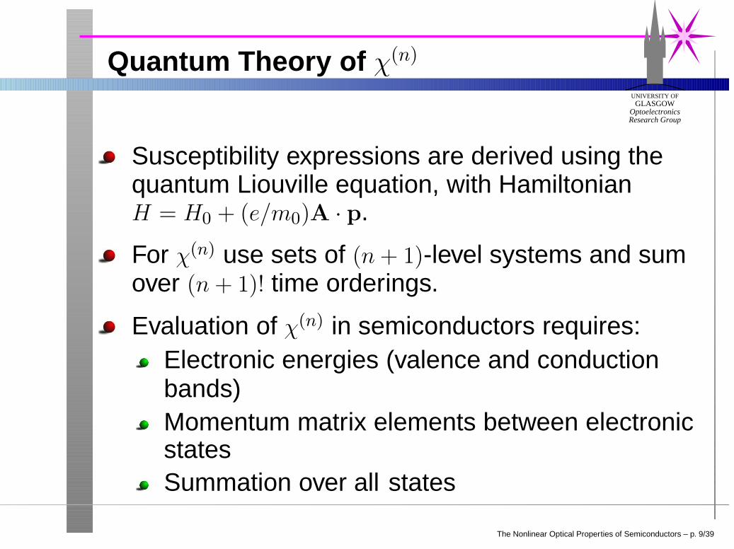
Susceptibility expressions are derived using thequantum Liouville equation, with HamiltonianH = H0 + (e/m0)A · p.
For χ(n) use sets of (n+ 1)-level systems and sumover (n+ 1)! time orderings.
Evaluation of χ(n) in semiconductors requires:Electronic energies (valence and conductionbands)Momentum matrix elements between electronicstatesSummation over all states
The Nonlinear Optical Properties of Semiconductors – p. 9/39
Research GroupOptoelectronics
GLASGOWUNIVERSITY OF
Linear absorption and refraction
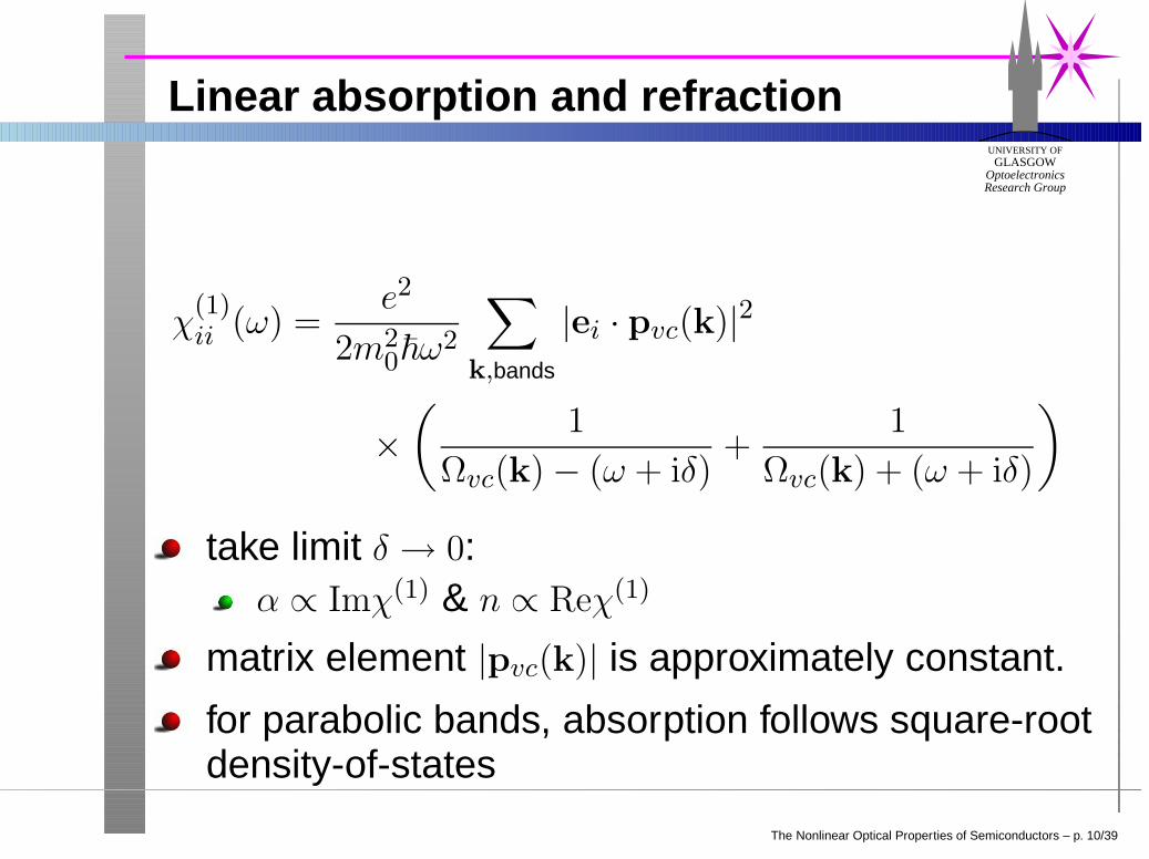
χ(1)ii (ω) =
e2
2m20~ω
2
∑
k,bands
|ei · pvc(k)|2
×(
1
Ωvc(k) − (ω + iδ)+
1
Ωvc(k) + (ω + iδ)
)
take limit δ → 0:α ∝ Imχ(1) & n ∝ Reχ(1)
matrix element |pvc(k)| is approximately constant.
for parabolic bands, absorption follows square-rootdensity-of-states
The Nonlinear Optical Properties of Semiconductors – p. 10/39

Research GroupOptoelectronics
GLASGOWUNIVERSITY OF
χ(1) for 2-level system
-7.5 -5 -2.5 2.5 5 7.5HΩ-WL∆
-0.4
-0.2
0.2
0.4
0.6
0.8
1
The Nonlinear Optical Properties of Semiconductors – p. 11/39

Research GroupOptoelectronics
GLASGOWUNIVERSITY OF
Linear refraction
Dispersion with parabolic bands gives Adachi formula
ε(ω) = A
f(X) +1
2
[
Eg
Eg + ∆
]3/2
f(Xso)
+B
f(X) = Re(2 −√
1 +X −√
1 −X)/X2 n =√ε
X =~ω
Eg=λg
λXso =
~ω
Eg + ∆
A(x) = 6.3 + 19.0x B(x) = 9.4 − 10.2x
Eg = (1.425 + 1.155x+ 0.37x2) eV ∆ = 0.34 eV
The Nonlinear Optical Properties of Semiconductors – p. 12/39

Research GroupOptoelectronics
GLASGOWUNIVERSITY OF
Linear refraction (300K)
800 1000 1200 1400 1600
3.3
3.4
3.5
3.6
3.7
3.8
Refractive index vs wavelength (nm)x =0, 0.1, 0.2, 0.3
The Nonlinear Optical Properties of Semiconductors – p. 13/39
Research GroupOptoelectronics
GLASGOWUNIVERSITY OF
Slowly varying envelope approx.
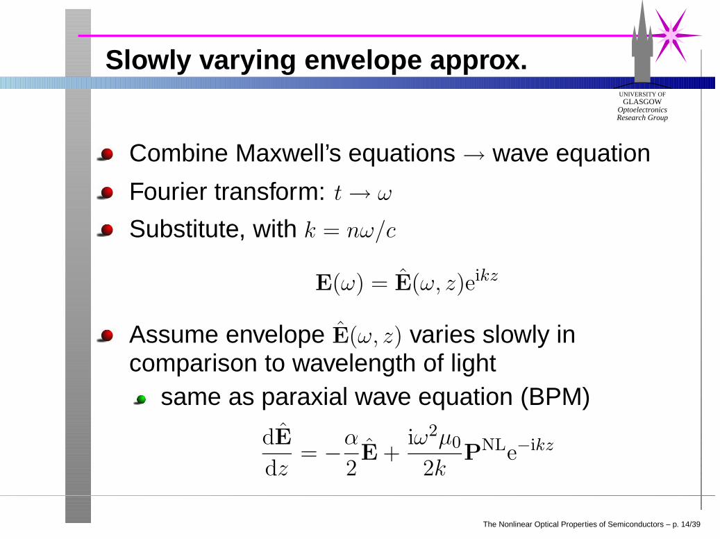
Combine Maxwell’s equations → wave equation
Fourier transform: t→ ω
Substitute, with k = nω/c
E(ω) = E(ω, z)eikz
Assume envelope E(ω, z) varies slowly incomparison to wavelength of light
same as paraxial wave equation (BPM)
dE
dz= −α
2E +
iω2µ0
2kPNLe−ikz
The Nonlinear Optical Properties of Semiconductors – p. 14/39

Research GroupOptoelectronics
GLASGOWUNIVERSITY OF
Second-order nonlinearities
No second-order nonlinearity in media withinversion symmetry
Crystal symmetry in cubic semiconductorsspecifies that the only non-zero tensor elementsare
χ(2)xyz = χ
(2)yzx = χ
(2)zxy
More independent tensor elements inheterostructures and at surfaces
The Nonlinear Optical Properties of Semiconductors – p. 15/39
Research GroupOptoelectronics
GLASGOWUNIVERSITY OF
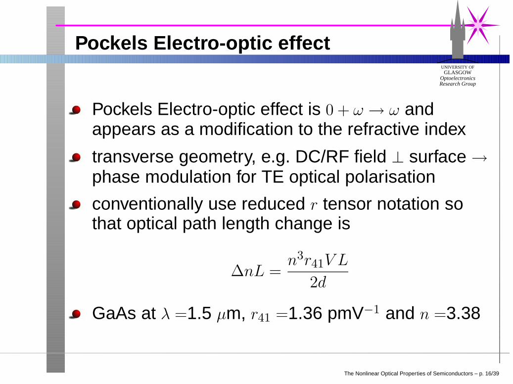
Pockels Electro-optic effect
Pockels Electro-optic effect is 0 + ω → ω andappears as a modification to the refractive index
transverse geometry, e.g. DC/RF field ⊥ surface →phase modulation for TE optical polarisation
conventionally use reduced r tensor notation sothat optical path length change is
∆nL =n3r41V L
2d
GaAs at λ =1.5 µm, r41 =1.36 pmV−1 and n =3.38
The Nonlinear Optical Properties of Semiconductors – p. 16/39

Research GroupOptoelectronics
GLASGOWUNIVERSITY OF
Frequency conversion by χ(2)
Optical frequency conversion (define ω3 = ω1 + ω2)sum frequency generation: ω1 + ω2 → ω3
second-harmonic generation: ω + ω → 2ω
difference frequency generation: ω3 − ω1 → ω2
parametric amplification: ω3 − ω1 → amplifies ω1
reduced d tensor notation, d = χ(2)(ω, ω)/2.
For epitaxial GaAs at λ =4.1 µm, d14 =94 pmV−1.
For continual forward energy conversion, requirePhase-matching, i.e. phase velocities ofgenerating and generated waves must be identical.
The Nonlinear Optical Properties of Semiconductors – p. 17/39
Research GroupOptoelectronics
GLASGOWUNIVERSITY OF
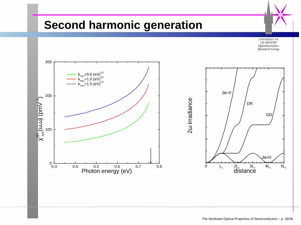
Second harmonic generation
0.3 0.4 0.5 0.6 0.7 0.8Photon energy (eV)
0
100
200
300
χ(2) xyz(
ω,ω
) (p
mV
−1 )
kmax=0.6 (eV)1/2
kmax=1.0 (eV)1/2
kmax=1.5 (eV)1/2
0 Lc 2Lc 3Lc 4Lc 5Lc
distance0.0
10.0
20.0
30.0
40.0
2ω Ir
radi
ance
∆k=0
DR
DD
∆k= / 0
The Nonlinear Optical Properties of Semiconductors – p. 18/39
Research GroupOptoelectronics
GLASGOWUNIVERSITY OF
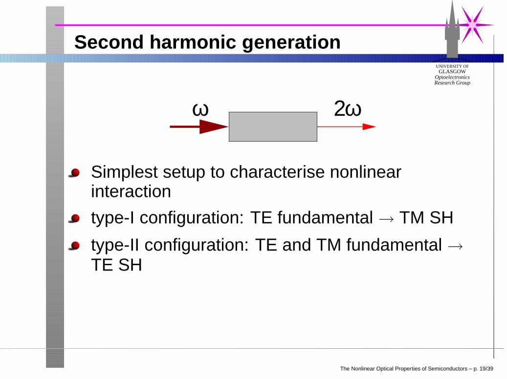
Second harmonic generation
ω 2ω
Simplest setup to characterise nonlinearinteraction
type-I configuration: TE fundamental → TM SH
type-II configuration: TE and TM fundamental →TE SH
The Nonlinear Optical Properties of Semiconductors – p. 19/39
Research GroupOptoelectronics
GLASGOWUNIVERSITY OF
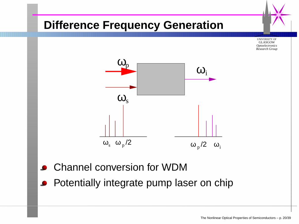
Difference Frequency Generation
ωs pω /2 ωipω /2
ωp ωi
ωs
Channel conversion for WDM
Potentially integrate pump laser on chip
The Nonlinear Optical Properties of Semiconductors – p. 20/39
Research GroupOptoelectronics
GLASGOWUNIVERSITY OF
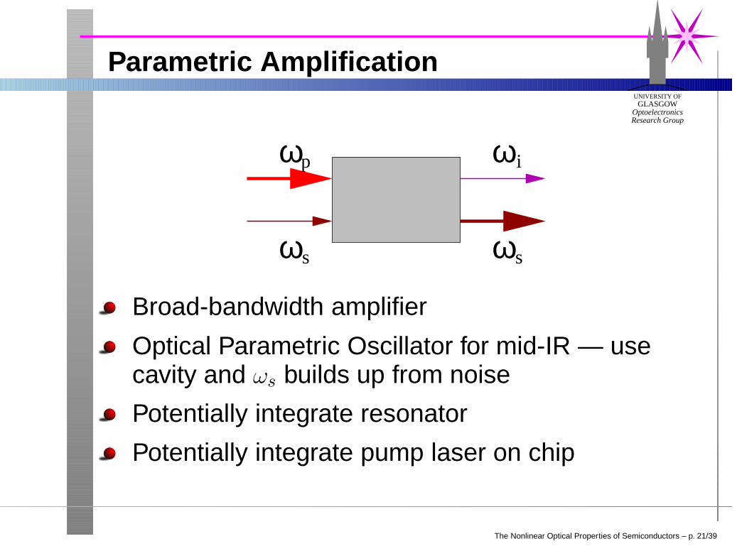
Parametric Amplification
ωp
ωs
ωi
ωs
Broad-bandwidth amplifier
Optical Parametric Oscillator for mid-IR — usecavity and ωs builds up from noise
Potentially integrate resonator
Potentially integrate pump laser on chip
The Nonlinear Optical Properties of Semiconductors – p. 21/39
Research GroupOptoelectronics
GLASGOWUNIVERSITY OF
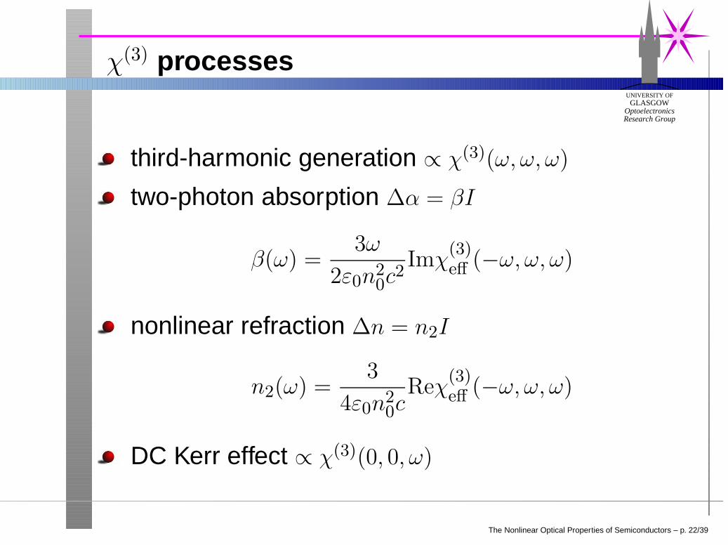
χ(3) processes
third-harmonic generation ∝ χ(3)(ω, ω, ω)
two-photon absorption ∆α = βI
β(ω) =3ω
2ε0n20c
2Imχ
(3)eff (−ω, ω, ω)
nonlinear refraction ∆n = n2I
n2(ω) =3
4ε0n20c
Reχ(3)eff (−ω, ω, ω)
DC Kerr effect ∝ χ(3)(0, 0, ω)
The Nonlinear Optical Properties of Semiconductors – p. 22/39

Research GroupOptoelectronics
GLASGOWUNIVERSITY OF
χ(3) symmetry considerations
4 independent nonzero tensor elements for bulksemiconductors
3 for single ω
χ(3)xxxx(−ω, ω, ω), χ(3)
xyxy(−ω, ω, ω), χ(3)xxyy(−ω, ω, ω)
Three measurements required to completelycharacterise each nonlinear process
Breaking symmetry, e.g. heterostructureintroduces many more independent nonzerotensor elements
The Nonlinear Optical Properties of Semiconductors – p. 23/39

Research GroupOptoelectronics
GLASGOWUNIVERSITY OF
Two-photon Absorption
0.7 0.8 0.9 1.0 1.1 1.2 1.3 1.4 1.5Photon Energy (eV)
0
2x10⁻¹⁹
4x10⁻¹⁹
6x10⁻¹⁹
8x10⁻¹⁹
Imχ(3
) (m
2 V−
2 )
xxxx
xyxy
xxyy
0.7 0.8 0.9 1.0 1.1 1.2 1.3 1.4 1.5Photon Energy (eV)
0
5
10
15
20
25
30
Tw
o-ph
oton
abs
orpt
ion
(cm
/GW
)
E||[111]
E||[011]
E||[001]
k||[111]
k||[011]
k||[001]
Calculated Imχ(3) tensor elements and spectra of βfor GaAs.
Scales as E−3g .
The Nonlinear Optical Properties of Semiconductors – p. 24/39

Research GroupOptoelectronics
GLASGOWUNIVERSITY OF
Ultrafast Nonlinear Refraction
Three measurements completely characterisenonlinear refraction in bulk (cubic) semiconductor
Strength nL2 [001] ∆n/I|[001]
Anisotropy σ 2
nL2 [001] − nL
2 [011]
/nL2 [001]
Biref. param. δ
nL2 [001] − nC
2 (k ‖ [100])
/nL2 [001]
n2 scales as E−4g
For isotropic Kleinmann: σ = 0, δ = 1/3
GaAs at the half-gap (theory): σ = −0.82, δ = 0.08
AlGaAs at the half-gap (exper.): σ = −0.54, δ = 0.18
The Nonlinear Optical Properties of Semiconductors – p. 25/39

Research GroupOptoelectronics
GLASGOWUNIVERSITY OF
Coupled Propagation Equations
Usual configuration in semiconductor slabwaveguides has TE‖[110] (cleavage planes) andTM‖[001].
i∂u
∂z+
∂2u
∂x2+ γu +
h
1 −
σ
2
uu∗
+
1 − δ −
σ
2
vv∗
iu +
δ −
σ
2
u∗v2= 0
i∂v
∂z+
∂2v
∂x2− γv +
h1 − δ −
σ
2
uu∗
+ vv∗
iv +
δ −
σ
2
u2v∗ = 0
u and v are the scaled electric field amplitudes forTE and TM.
γ is proportional to the (structurally induced)birefringence nTM − nTE.
The Nonlinear Optical Properties of Semiconductors – p. 26/39
Research GroupOptoelectronics
GLASGOWUNIVERSITY OF
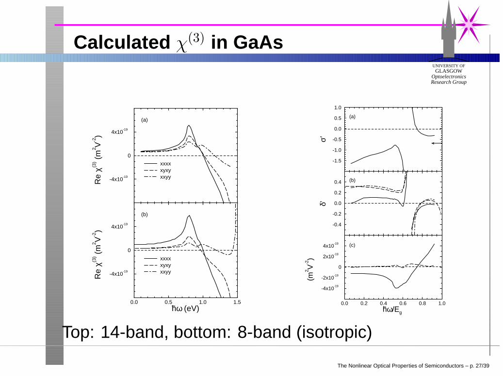
Calculated χ(3) in GaAs
-4x10-19
0
4x10-19
Re
χ(3) (
m2 V
-2)
xxxxxyxyxxyy
0.0 0.5 1.0 1.5hω (eV)
-4x10-19
0
4x10-19
Re
χ(3) (
m2 V
-2)
xxxxxyxyxxyy
(b)
(a)
-1.5
-1.0
-0.5
0.0
0.5
1.0
σ’
-0.4
-0.2
0.0
0.2
0.4
δ’
0.0 0.2 0.4 0.6 0.8 1.0hω/Eg
-4x10-19
-2x10-19
0
2x10-19
4x10-19
(m2 V
-2)
(c)
(b)
(a)
Top: 14-band, bottom: 8-band (isotropic)
The Nonlinear Optical Properties of Semiconductors – p. 27/39

Research GroupOptoelectronics
GLASGOWUNIVERSITY OF
n2 in Al 0.18Ga0.82As
1.4 1.5 1.6 1.7Wavelength (µm)
0
1x10-13
2x10-13
3x10-13
n 2 (c
m2 W
-1)
0.4 0.5 0.6 0.7 0.8 0.9
Photon energy (eV)
0
50000
100000
150000
200000
250000
300000
Reχ
(3) (
pm/V
)2
xxxxxxyyxyxy
Measured dispersion of n2 in Al0.18Ga0.82As andcalculated Reχ(3) tensor components
The Nonlinear Optical Properties of Semiconductors – p. 28/39
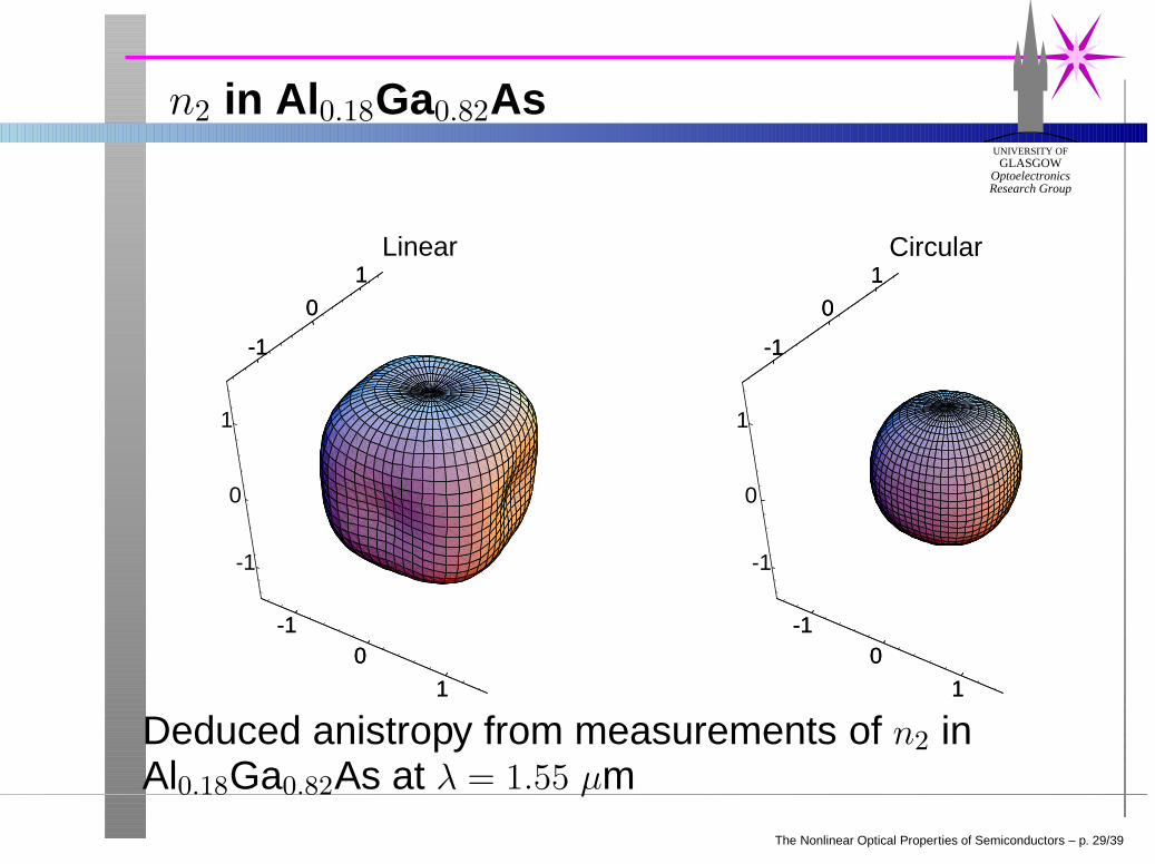
Research GroupOptoelectronics
GLASGOWUNIVERSITY OF
n2 in Al 0.18Ga0.82As
Linear
-10
1
-1
0
1
-1
0
1
-10
1
-1
0
1Circular
-10
1
-1
0
1
-1
0
1
-10
1
-1
0
1
Deduced anistropy from measurements of n2 inAl0.18Ga0.82As at λ = 1.55 µm
The Nonlinear Optical Properties of Semiconductors – p. 29/39

Research GroupOptoelectronics
GLASGOWUNIVERSITY OF
Figure-of-merit for NLR applications
light absorbed inlength α−1
phase change2π|∆n|L/λ ∼ 2π forNLO applications
therefore requirefigure-of-merit|∆n|/(αλ) > 1
for χ(3) only, figure-of-merit |n2|/(βλ) ∝|Reχ(3)|/Imχ(3)
0.5 0.6 0.7 0.8 0.9 1.0hω/Eg
0.1
1.0
10.0
100.0
|Reχ
(3) |/I
mχ(3
)
NLDC
FP
The Nonlinear Optical Properties of Semiconductors – p. 30/39
Research GroupOptoelectronics
GLASGOWUNIVERSITY OF
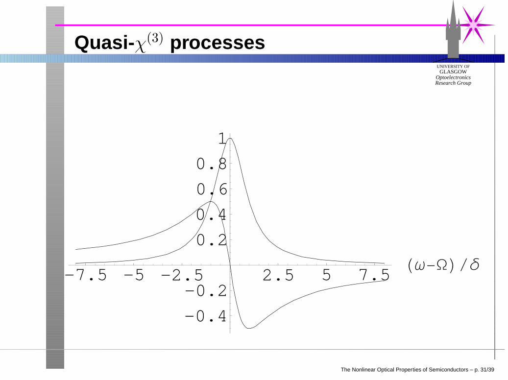
Quasi-χ(3) processes
-7.5 -5 -2.5 2.5 5 7.5HΩ-WL∆
-0.4
-0.2
0.2
0.4
0.6
0.8
1
The Nonlinear Optical Properties of Semiconductors – p. 31/39

Research GroupOptoelectronics
GLASGOWUNIVERSITY OF
Carrier nonlinearities
Free carrier absorption: N ↑, α ↑Absorption saturation (bandfilling) in passivedevice: N ↑, α ↓, n ↓Gain saturation in active device: N ↓, gain↓, n ↑Exciton absorption saturation (phase-space filling+ screening): N ↑, α ↓, n ↓
N.B. effects on n are for below bandgap frequencies
The Nonlinear Optical Properties of Semiconductors – p. 32/39

Research GroupOptoelectronics
GLASGOWUNIVERSITY OF
Example: bandfilling
Assuming equal populations N of electrons andheavy-holes which have quasi-equilibrium Boltzmannthermal distribution, we get ∆n = σnN
σn(ω) = −4√π
n0
∣
∣
∣
∣
epvc
m0ωg
∣
∣
∣
∣
21
kBT
∑
j=hh,lh
mrj
meJ
(
mrj
me
~(ω − ωg)
kBT
)
The Nonlinear Optical Properties of Semiconductors – p. 33/39
Research GroupOptoelectronics
GLASGOWUNIVERSITY OF
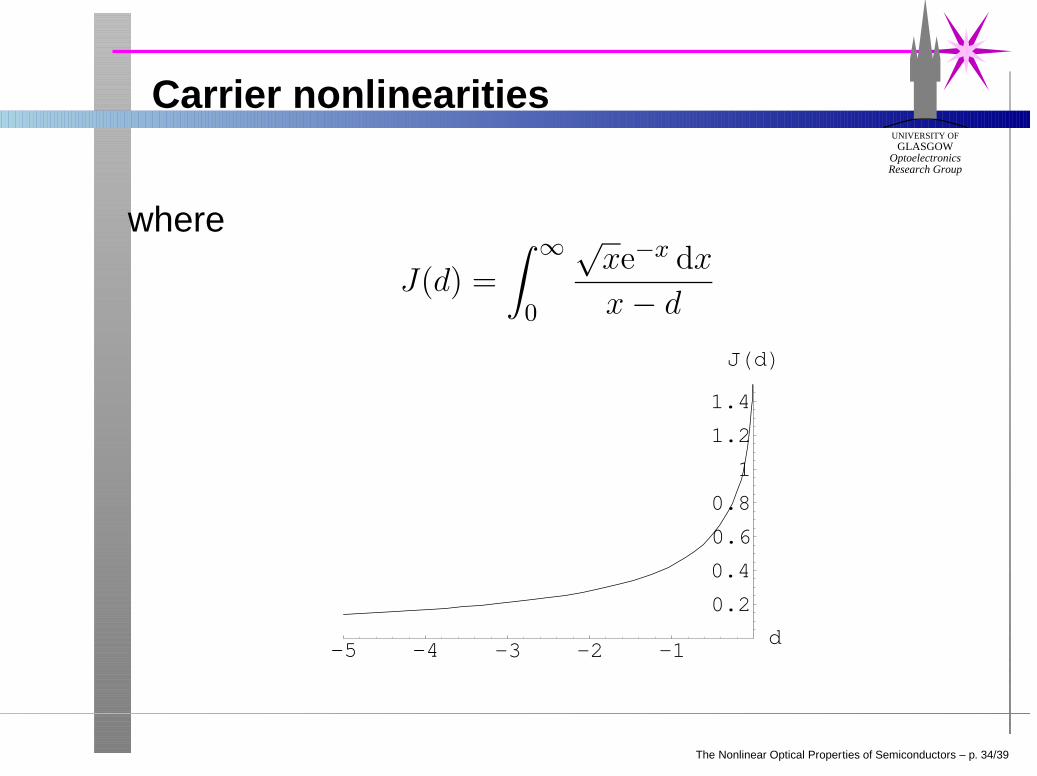
Carrier nonlinearities
where
J(d) =
∫
∞
0
√xe−x dx
x− d
-5 -4 -3 -2 -1d
0.2
0.4
0.6
0.8
1
1.2
1.4
JHdL
The Nonlinear Optical Properties of Semiconductors – p. 34/39
Research GroupOptoelectronics
GLASGOWUNIVERSITY OF
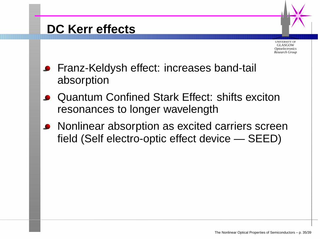
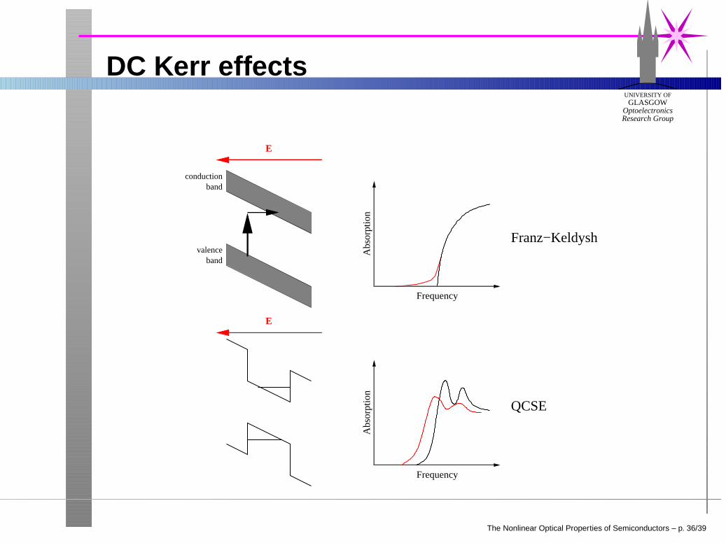
DC Kerr effects
Franz-Keldysh effect: increases band-tailabsorption
Quantum Confined Stark Effect: shifts excitonresonances to longer wavelength
Nonlinear absorption as excited carriers screenfield (Self electro-optic effect device — SEED)
The Nonlinear Optical Properties of Semiconductors – p. 35/39
Research GroupOptoelectronics
GLASGOWUNIVERSITY OF
DC Kerr effects
QCSE
Frequency
Abs
orpt
ion
Frequency
Abs
orpt
ion
conductionband
valenceband
E
E
Franz−Keldysh
The Nonlinear Optical Properties of Semiconductors – p. 36/39

Research GroupOptoelectronics
GLASGOWUNIVERSITY OF
Thermal effects
Absorbed light results in heating of medium andchanges linear optical properties
∂n
∂T=
∂n
∂Eg
∂Eg
∂T
For AlxGa1−xAs∂Eg/∂T = −(3.95 + 1.15x) × 10−4 eVK−1.
Can differentiate Adachi formula for ∂n/∂Eg
∂n/∂Eg < 0 below bandgapgiving ∂n/∂T > 0 generallye.g. 6.5 × 10⁻⁵ K−1 in GaAs at 1.5 µm
The Nonlinear Optical Properties of Semiconductors – p. 37/39
Research GroupOptoelectronics
GLASGOWUNIVERSITY OF
Bibliography (materials)
1. S. Adachi, “GaAs, AlAs and AlxGa1−xAs: Material parameters for use in researchand device applications”, J. Appl. Phys. 58, R1 (1985).
2. “Properties of Gallium Arsenide”, INSPEC (1990).
3. Ioffe Physico-Technical Institute Electronic Archive on Semiconductorshttp://www.ioffe.rssi.ru/SVA/NSM/
4. E. O. Kane, J. Phys. Chem. Solids 1, 249 (1957).
5. P. Pfeffer & W. Zawadzki, “Conduction electrons in GaAs — 5-level k.p theory andpolaron effects”, Phys. Rev. B 41, 1561 (1990).
6. G. Bastard, “Wave mechanics applied to semiconductor heterostructures” (LesEditions de Physique, 1989).
The Nonlinear Optical Properties of Semiconductors – p. 38/39

Research GroupOptoelectronics
GLASGOWUNIVERSITY OF
Bibliography (NLO)
1. P. N. Butcher & D. Cotter, “The Elements of Nonlinear Optics” (CambridgeUniversity Press, 1990).
2. Y. R. Shen, “The Principles of Nonlinear Optics” (Wiley, 1984).
3. A. Yariv, “Quantum Electronics” (Wiley, 1989).
4. D. C. Hutchings, “Applied Nonlinear Optics”,http://userweb.elec.gla.ac.uk/d/dch/course.pdf
5. D. C. Hutchings, et al, “Kramers-Krönig relations in nonlinear optics”, Opt. andQuant. Electr. 24, 1 (1992).
6. D. C. Hutchings & B. S. Wherrett, “Theory of Anisotropy of Two-Photon Absorptionin Zinc-Blende Semiconductors”, Phys. Rev. B 49, 2418 (1994).
7. D. C. Hutchings & B. S. Wherrett, “Theory of the Anisotropy of Ultrafast NonlinearRefraction in Zinc-Blende Semiconductors”, Phys. Rev. B 52, 8150 (1995).
8. J. S. Aitchison, et al, “The Nonlinear Optical Properties of AlGaAs at theHalf-Band-Gap”, IEEE J. Quantum Electron. 33, 341 (1997).
The Nonlinear Optical Properties of Semiconductors – p. 39/39