TDA7375A - Octopartdatasheet.octopart.com/TDA7375AV-STMicroelectronics-datasheet... · TDA7375A...
15
1/15 TDA7375A March 2005 1 FEATURES ■ HIGH OUTPUT POWER CAPABILITY: – 2 x 43W max./4Ω – 2 x 37W/4Ω EIAJ – 2 x 26W/4Ω @14.4V, 1KHz, 10% – 4 x 7W/4Ω @14.4V,1KHz, 10% – 4 x 12W/2Ω @14.4V, 1KHz, 10% ■ MINIMUM EXTERNAL COMPONENTS COUNT: – NO BOOTSTRAP CAPACITORS – NO BOUCHEROT CELLS – INTERNALLY FIXED GAIN (26dB BTL) ■ ST-BY FUNCTION (CMOS COMPATIBLE) ■ NO AUDIBLE POP DURING ST-BY OPERATIONS ■ DIAGNOSTICS FACILITY FOR: – CLIPPING – OUT TO GND SHORT – OUT TO V S SHORT – SOFT SHORT AT TURN-ON – THERMAL SHUTDOWN PROXIMITY 2 PROTECTIONS: ■ OUPUT AC/DC SHORT CIRCUIT – TO GND – TO V S – ACROSS THE LOAD ■ SOFT SHORT AT TURN-ON ■ OVERRATING CHIP TEMPERATURE WITH SOFT THERMAL LIMITER ■ LOAD DUMP VOLTAGE SURGE ■ VERY INDUCTIVE LOADS ■ FORTUITOUS OPEN GND ■ REVERSED BATTERY ■ ESD 2 X 37W DUAL/QUAD POWER AMPLIFIER FOR CAR RADIO Figure 2. Block Diagram Rev. 2 Figure 1. Package Table 1. Order Codes Part Number Package TDA7375AV MULTIWATT 15 (Vertical) MULTIWATT15
Transcript of TDA7375A - Octopartdatasheet.octopart.com/TDA7375AV-STMicroelectronics-datasheet... · TDA7375A...
TDA7375A
March 2005
2 X 37W DUAL/QUAD POWER AMPLIFIER FOR CAR RADIO
Figure 1. Package
Table 1. Order Codes
Part Number Package
TDA7375AV MULTIWATT 15 (Vertical)
MULTIWATT15
1 FEATURES HIGH OUTPUT POWER CAPABILITY:
– 2 x 43W max./4Ω– 2 x 37W/4Ω EIAJ– 2 x 26W/4Ω @14.4V, 1KHz, 10%– 4 x 7W/4Ω @14.4V,1KHz, 10%– 4 x 12W/2Ω @14.4V, 1KHz, 10%
MINIMUM EXTERNAL COMPONENTS COUNT:
– NO BOOTSTRAP CAPACITORS– NO BOUCHEROT CELLS– INTERNALLY FIXED GAIN (26dB BTL)
ST-BY FUNCTION (CMOS COMPATIBLE)
NO AUDIBLE POP DURING ST-BY OPERATIONS
DIAGNOSTICS FACILITY FOR:
– CLIPPING– OUT TO GND SHORT– OUT TO VS SHORT– SOFT SHORT AT TURN-ON– THERMAL SHUTDOWN PROXIMITY
2 PROTECTIONS: OUPUT AC/DC SHORT CIRCUIT
– TO GND– TO VS– ACROSS THE LOAD
SOFT SHORT AT TURN-ON OVERRATING CHIP TEMPERATURE WITH
SOFT THERMAL LIMITER LOAD DUMP VOLTAGE SURGE VERY INDUCTIVE LOADS FORTUITOUS OPEN GND REVERSED BATTERY ESD
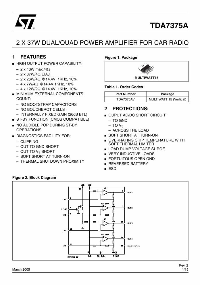
Figure 2. Block Diagram
1/15Rev. 2
TDA7375A
3 DESCRIPTIONThe TDA7375A is a new technology class AB car radio amplifier able to work either in DUAL BRIDGE orQUAD SINGLE ENDED configuration.
The exclusive fully complementary structure of the output stage and the internally fixed gain guarantee thehighest possible power performances with extremely reduced component count.
The on-board clip detector simplifies gain compression operation. The fault diagnostics makes it possibleto detect mistakes during car radio set assembly and wiring in the car.
Table 2. Absolute Maximum Ratings
Table 3. Thermal Data
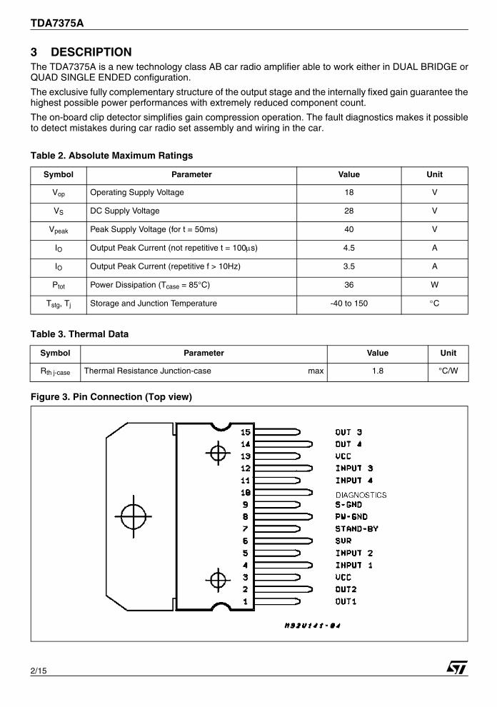
Figure 3. Pin Connection (Top view)
Symbol Parameter Value Unit
Vop Operating Supply Voltage 18 V
VS DC Supply Voltage 28 V
Vpeak Peak Supply Voltage (for t = 50ms) 40 V
IO Output Peak Current (not repetitive t = 100µs) 4.5 A
IO Output Peak Current (repetitive f > 10Hz) 3.5 A
Ptot Power Dissipation (Tcase = 85°C) 36 W
Tstg, Tj Storage and Junction Temperature -40 to 150 °C
Symbol Parameter Value Unit
Rth j-case Thermal Resistance Junction-case max 1.8 °C/W
2/15
TDA7375A
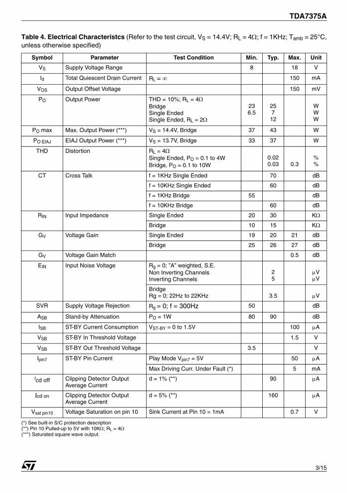
Table 4. Electrical Characteristcs (Refer to the test circuit, VS = 14.4V; RL = 4Ω; f = 1KHz; Tamb = 25°C,unless otherwise specified)
(*) See built-in S/C protection description(**) Pin 10 Pulled-up to 5V with 10KΩ; RL = 4Ω(***) Saturated square wave output.
Symbol Parameter Test Condition Min. Typ. Max. Unit
VS Supply Voltage Range 8 18 V
Id Total Quiescent Drain Current RL = ∞ 150 mA
VOS Output Offset Voltage 150 mV
PO Output Power THD = 10%; RL = 4ΩBridgeSingle EndedSingle Ended, RL = 2Ω
236.5
25712
WWW
PO max Max. Output Power (***) VS = 14.4V, Bridge 37 43 W
PO EIAJ EIAJ Output Power (***) VS = 13.7V, Bridge 33 37 W
THD Distortion RL = 4ΩSingle Ended, PO = 0.1 to 4WBridge, PO = 0.1 to 10W
0.020.03 0.3
%%
CT Cross Talk f = 1KHz Single Ended 70 dB
f = 10KHz Single Ended 60 dB
f = 1KHz Bridge 55 dB
f = 10KHz Bridge 60 dB
RIN Input Impedance Single Ended 20 30 KΩ
Bridge 10 15 KΩ
GV Voltage Gain Single Ended 19 20 21 dB
Bridge 25 26 27 dB
GV Voltage Gain Match 0.5 dB
EIN Input Noise Voltage Rg = 0; ”A” weighted, S.E.Non Inverting ChannelsInverting Channels
25
µVµV
BridgeRg = 0; 22Hz to 22KHz 3.5 µV
SVR Supply Voltage Rejection Rg = 0; f = 300Hz 50 dB
ASB Stand-by Attenuation PO = 1W 80 90 dB
ISB ST-BY Current Consumption VST-BY = 0 to 1.5V 100 µA
VSB ST-BY In Threshold Voltage 1.5 V
VSB ST-BY Out Threshold Voltage 3.5 V
Ipin7 ST-BY Pin Current Play Mode Vpin7 = 5V 50 µA
Max Driving Curr. Under Fault (*) 5 mA
Icd off Clipping Detector Output Average Current
d = 1% (**) 90 µA
Icd on Clipping Detector Output Average Current
d = 5% (**) 160 µA
Vsat pin10 Voltage Saturation on pin 10 Sink Current at Pin 10 = 1mA 0.7 V
3/15
TDA7375A
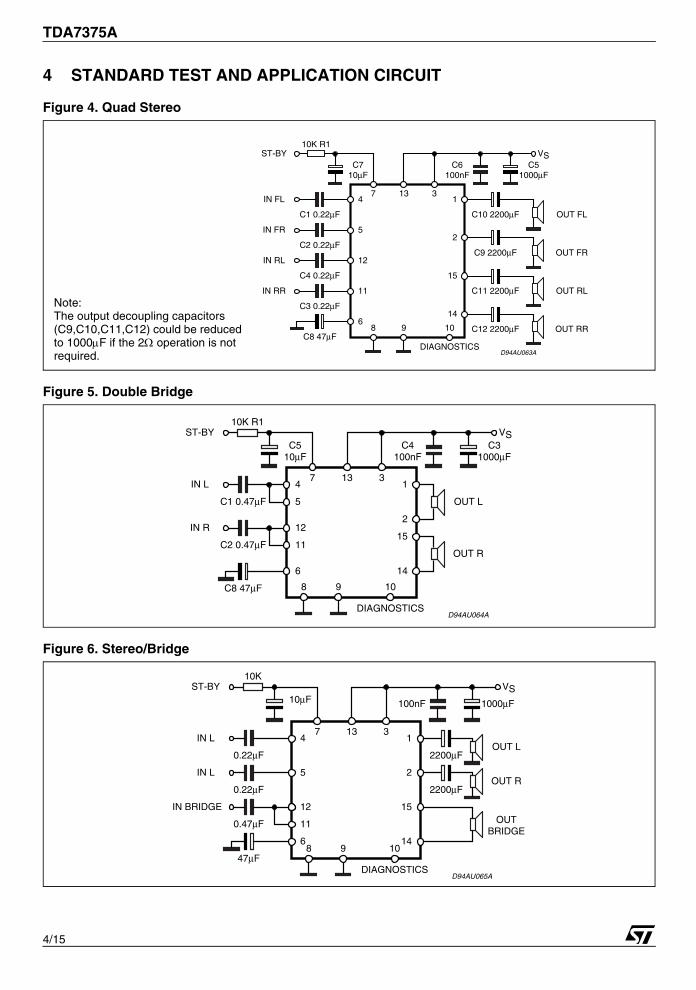
4 STANDARD TEST AND APPLICATION CIRCUIT
Figure 4. Quad Stereo
Figure 5. Double Bridge
Figure 6. Stereo/Bridge
C1 0.22µF
1
DIAGNOSTICS
47
C10 2200µF
D94AU063A
C710µF
10K R1ST-BY
IN FL
C2 0.22µF
IN FR 5
C4 0.22µF
12IN RL
C3 0.22µF
IN RR 11
C8 47µF
6
13
C51000µF
C6100nF
3
VS
C9 2200µF
2
15
C11 2200µF
C12 2200µF
14
OUT FL
OUT FR
OUT RL
OUT RR8 9 10
Note:The output decoupling capacitors(C9,C10,C11,C12) could be reduced to 1000µF if the 2Ω operation is notrequired.
C1 0.47µF
1
DIAGNOSTICS
47
D94AU064A
C510µF
10K R1ST-BY
IN L
C2 0.47µF
5
12IN R
11
C8 47µF
6
13
C31000µF
C4100nF
3
VS
2
15
14
OUT L
8 9 10
OUT R
0.22µF
1
DIAGNOSTICS
47
D94AU065A
10µF
10KST-BY
IN L
0.47µF
5
IN BRIDGE 12
47µF
6
13
1000µF100nF
3
VS
2
15
14
OUT L
8 9 10
OUTBRIDGE
11
0.22µF
IN LOUT R
2200µF
2200µF
4/15
TDA7375A
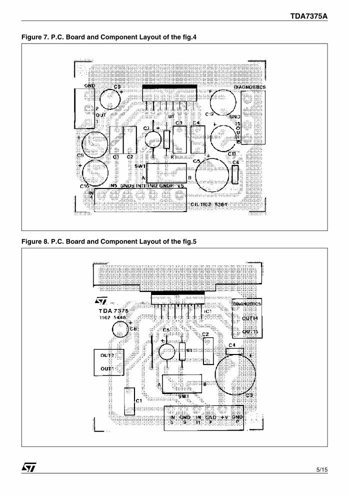
Figure 7. P.C. Board and Component Layout of the fig.4
Figure 8. P.C. Board and Component Layout of the fig.5
5/15
TDA7375A
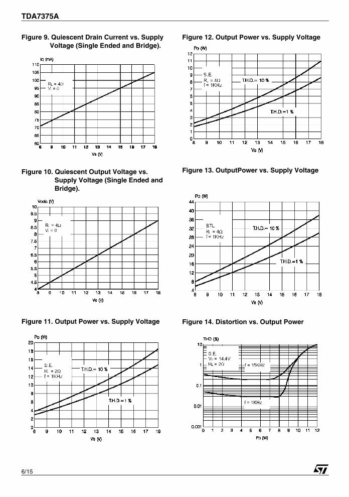
Figure 9. Quiescent Drain Current vs. Supply Voltage (Single Ended and Bridge).
Figure 10. Quiescent Output Voltage vs. Supply Voltage (Single Ended and Bridge).
Figure 11. Output Power vs. Supply Voltage
Figure 12. Output Power vs. Supply Voltage
Figure 13. OutputPower vs. Supply Voltage
Figure 14. Distortion vs. Output Power
6/15
TDA7375A
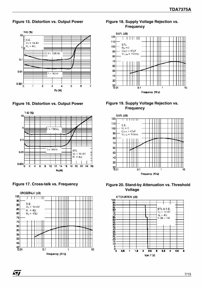
Figure 15. Distortion vs. Output Power
Figure 16. Distortion vs. Output Power
Figure 17. Cross-talk vs. Frequency
Figure 18. Supply Voltage Rejection vs. Frequency
Figure 19. Supply Voltage Rejection vs. Frequency
Figure 20. Stand-by Attenuation vs. Threshold Voltage
7/15
TDA7375A
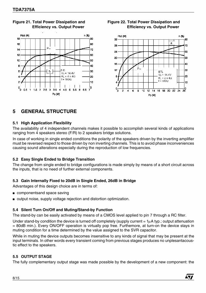
Figure 21. Total Power Dissipation and Efficiency vs. Output Power
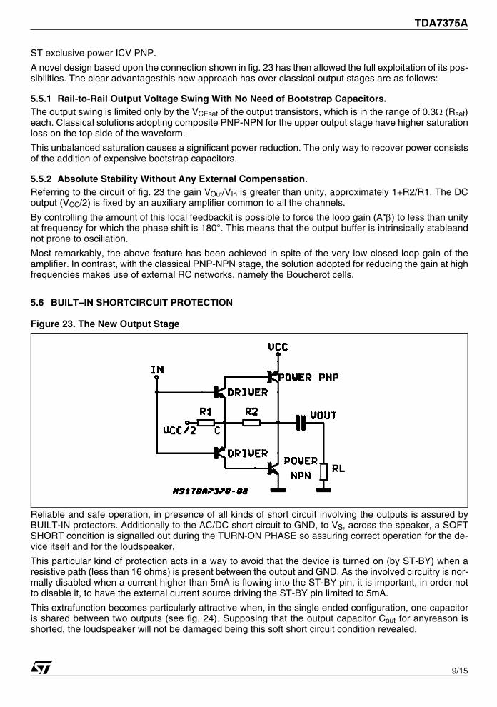
Figure 22. Total Power Dissipation and Efficiency vs. Output Power
5 GENERAL STRUCTURE
5.1 High Application FlexibilityThe availability of 4 independent channels makes it possible to accomplish several kinds of applicationsranging from 4 speakers stereo (F/R) to 2 speakers bridge solutions.
In case of working in single ended conditions the polarity of the speakers driven by the inverting amplifiermust be reversed respect to those driven by non inverting channels. This is to avoid phase inconveniencescausing sound alterations especially during the reproduction of low frequencies.
5.2 Easy Single Ended to Bridge TransitionThe change from single ended to bridge configurations is made simply by means of a short circuit acrossthe inputs, that is no need of further external components.
5.3 Gain Internally Fixed to 20dB in Single Ended, 26dB in BridgeAdvantages of this design choice are in terms of:
componentsand space saving
output noise, supply voltage rejection and distortion optimization.
5.4 Silent Turn On/Off and Muting/Stand-by FunctionThe stand-by can be easily activated by means of a CMOS level applied to pin 7 through a RC filter.
Under stand-by condition the device is turned off completely (supply current = 1µA typ.; output attenuation= 80dB min.). Every ON/OFF operation is virtually pop free. Furthemore, at turn-on the device stays inmuting condition for a time determined by the value assigned to the SVR capacitor.
While in muting the device outputs becomes insensitive to any kinds of signal that may be present at theinput terminals. In other words every transient coming from previous stages produces no unplesantacous-tic effect to the speakers.
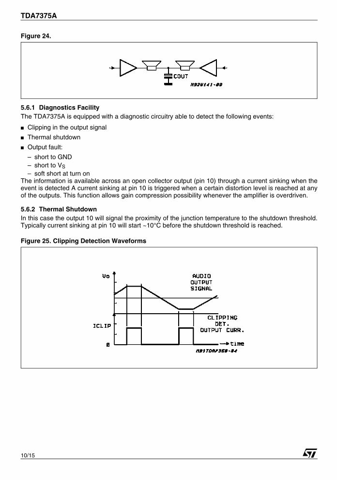
5.5 OUTPUT STAGEThe fully complementary output stage was made possible by the development of a new component: the
8/15
TDA7375A
ST exclusive power ICV PNP.
A novel design based upon the connection shown in fig. 23 has then allowed the full exploitation of its pos-sibilities. The clear advantagesthis new approach has over classical output stages are as follows:
5.5.1 Rail-to-Rail Output Voltage Swing With No Need of Bootstrap Capacitors.The output swing is limited only by the VCEsat of the output transistors, which is in the range of 0.3Ω (Rsat)each. Classical solutions adopting composite PNP-NPN for the upper output stage have higher saturationloss on the top side of the waveform.
This unbalanced saturation causes a significant power reduction. The only way to recover power consistsof the addition of expensive bootstrap capacitors.
5.5.2 Absolute Stability Without Any External Compensation.Referring to the circuit of fig. 23 the gain VOut/VIn is greater than unity, approximately 1+R2/R1. The DCoutput (VCC/2) is fixed by an auxiliary amplifier common to all the channels.
By controlling the amount of this local feedbackit is possible to force the loop gain (A*β) to less than unityat frequency for which the phase shift is 180°. This means that the output buffer is intrinsically stableandnot prone to oscillation.
Most remarkably, the above feature has been achieved in spite of the very low closed loop gain of theamplifier. In contrast, with the classical PNP-NPN stage, the solution adopted for reducing the gain at highfrequencies makes use of external RC networks, namely the Boucherot cells.
5.6 BUILT–IN SHORTCIRCUIT PROTECTION
Figure 23. The New Output Stage
Reliable and safe operation, in presence of all kinds of short circuit involving the outputs is assured byBUILT-IN protectors. Additionally to the AC/DC short circuit to GND, to VS, across the speaker, a SOFTSHORT condition is signalled out during the TURN-ON PHASE so assuring correct operation for the de-vice itself and for the loudspeaker.
This particular kind of protection acts in a way to avoid that the device is turned on (by ST-BY) when aresistive path (less than 16 ohms) is present between the output and GND. As the involved circuitry is nor-mally disabled when a current higher than 5mA is flowing into the ST-BY pin, it is important, in order notto disable it, to have the external current source driving the ST-BY pin limited to 5mA.
This extrafunction becomes particularly attractive when, in the single ended configuration, one capacitoris shared between two outputs (see fig. 24). Supposing that the output capacitor Cout for anyreason isshorted, the loudspeaker will not be damaged being this soft short circuit condition revealed.
9/15
TDA7375A
Figure 24.
5.6.1 Diagnostics FacilityThe TDA7375A is equipped with a diagnostic circuitry able to detect the following events:
Clipping in the output signal
Thermal shutdown
Output fault:
– short to GND– short to VS– soft short at turn on
The information is available across an open collector output (pin 10) through a current sinking when theevent is detected A current sinking at pin 10 is triggered when a certain distortion level is reached at anyof the outputs. This function allows gain compression possibility whenever the amplifier is overdriven.
5.6.2 Thermal ShutdownIn this case the output 10 will signal the proximity of the junction temperature to the shutdown threshold.Typically current sinking at pin 10 will start ~10°C before the shutdown threshold is reached.
Figure 25. Clipping Detection Waveforms
10/15

TDA7375A
Figure 26. Output Fault Waveforms (see fig. 27)
Figure 27. Fault Waveforms
5.7 HANDLING OF THE DIAGNOSTICS INFORMATIONAs various kinds of information is available at the same pin (clipping detection, output fault, thermal prox-imity), this signal must be handled properly in order to discriminate each event.
This could be done by taking into account the different timing of the diagnostic output during each case.
Normally the clip detector signalling produces a low level at pin 10 that is shorter referred to everyt kind offault detection; based on this assumption an interface circuitry to differentiate the information
11/15
TDA7375A
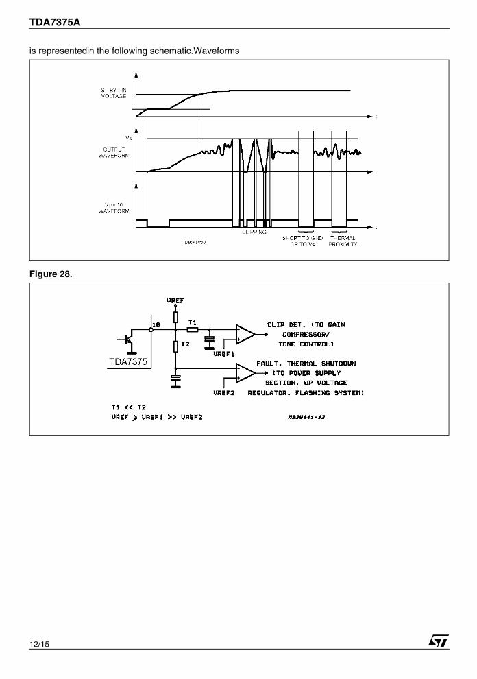
is representedin the following schematic.Waveforms
Figure 28.
12/15
TDA7375A
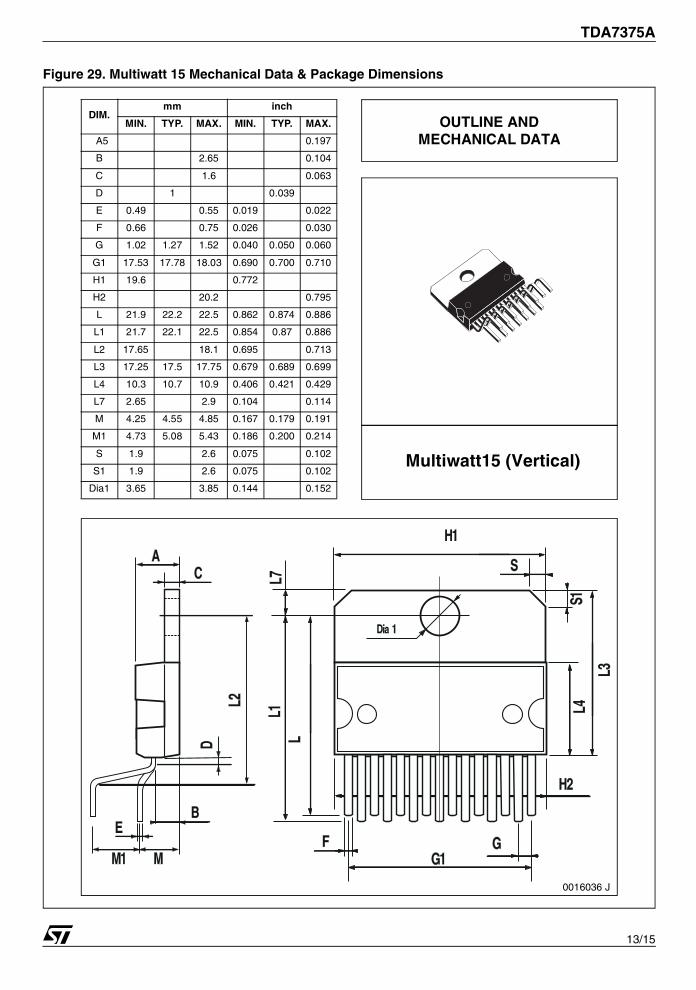
Figure 29. Multiwatt 15 Mechanical Data & Package Dimensions
OUTLINE ANDMECHANICAL DATA
0016036 J
DIM.mm inch
MIN. TYP. MAX. MIN. TYP. MAX.
A5 0.197
B 2.65 0.104
C 1.6 0.063
D 1 0.039
E 0.49 0.55 0.019 0.022
F 0.66 0.75 0.026 0.030
G 1.02 1.27 1.52 0.040 0.050 0.060
G1 17.53 17.78 18.03 0.690 0.700 0.710
H1 19.6 0.772
H2 20.2 0.795
L 21.9 22.2 22.5 0.862 0.874 0.886
L1 21.7 22.1 22.5 0.854 0.87 0.886
L2 17.65 18.1 0.695 0.713
L3 17.25 17.5 17.75 0.679 0.689 0.699
L4 10.3 10.7 10.9 0.406 0.421 0.429
L7 2.65 2.9 0.104 0.114
M 4.25 4.55 4.85 0.167 0.179 0.191
M1 4.73 5.08 5.43 0.186 0.200 0.214
S 1.9 2.6 0.075 0.102
S1 1.9 2.6 0.075 0.102
Dia1 3.65 3.85 0.144 0.152
Multiwatt15 (Vertical)
13/15
TDA7375A
6 REVISION HISTORY
Table 5. Revision History
Date Revision Description of Changes
July 2004 1 First Issue in EDOCS
March 2005 2 Changed the Style-sheet in compliance to the new “Corporate Technical Pubblications Design Guide”.Deleted package Mukltiwatt15 Horizontal
14/15
Information furnished is believed to be accurate and reliable. However, STMicroelectronics assumes no responsibility for the consequencesof use of such information nor for any infringement of patents or other rights of third parties which may result from its use. No license is grantedby implication or otherwise under any patent or patent rights of STMicroelectronics. Specifications mentioned in this publication are subjectto change without notice. This publication supersedes and replaces all information previously supplied. STMicroelectronics products are notauthorized for use as critical components in life support devices or systems without express written approval of STMicroelectronics.
The ST logo is a registered trademark of STMicroelectronics.All other names are the property of their respective owners
© 2005 STMicroelectronics - All rights reserved
STMicroelectronics group of companiesAustralia - Belgium - Brazil - Canada - China - Czech Republic - Finland - France - Germany - Hong Kong - India - Israel - Italy - Japan -
Malaysia - Malta - Morocco - Singapore - Spain - Sweden - Switzerland - United Kingdom - United States of Americawww.st.com
15/15
TDA7375A