TAS5182: 100-W Stereo Digital Amplifier Power Stage ... · 100−w stereo digital amplifier power...
19
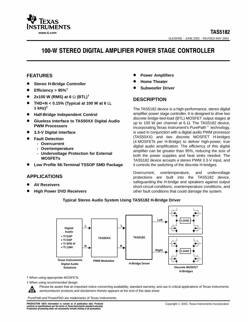
TAS5182 SLES045E - JUNE 2002 - REVISED MAY 2004 100-W STEREO DIGITAL AMPLIFIER POWER STAGE CONTROLLER FEATURES D Stereo H-Bridge Controller D Efficiency > 95% † D 2x100 W (RMS) at 6 Ω (BTL) † D THD+N < 0.15% (Typical at 100 W at 6 Ω, 1 kHz) ‡ D Half-Bridge Independent Control D Glueless Interface to TAS50XX Digital Audio PWM Processors D 3.3-V Digital Interface D Fault Detection - Overcurrent - Overtemperature - Undervoltage Protection for External MOSFETs D Low Profile 56-Terminal TSSOP SMD Package APPLICATIONS D AV Receivers D High Power DVD Receivers D Power Amplifiers D Home Theater D Subwoofer Driver DESCRIPTION The TAS5182 device is a high-performance, stereo digital amplifier power stage controller. It is designed to drive two discrete bridge-tied-load (BTL) MOSFET output stages at up to 100 W per channel at 6 Ω. The TAS5182 device, incorporating Texas Instrument’s PurePatht technology, is used in conjunction with a digital audio PWM processor (TAS50XX) and two discrete MOSFET H-bridges (4 MOSFETs per H-Bridge) to deliver high-power, true digital audio amplification. The efficiency of this digital amplifier can be greater than 95%, reducing the size of both the power supplies and heat sinks needed. The TAS5182 device accepts a stereo PWM 3.3-V input, and it controls the switching of the discrete H-bridges. Overcurrent, overtemperature, and undervoltage protections are built into the TAS5182 device, safeguarding the H-bridge and speakers against output short-circuit conditions, overtemperature conditions, and other fault conditions that could damage the system. Left Right PWM Modulator H-Bridges Texas Instruments Digital Audio Solutions TAS50XX TAS5182 Discrete MOSFET L L R R LOAD LOAD Digital Audio • TI DAP • TI DSP • TI SPD IF • TI 1394 H-Bridge Driver Typical Stereo Audio System Using TAS5182 H-Bridge Driver † When using appropriate MOSFETs. ‡ When using recommended design. Please be aware that an important notice concerning availability, standard warranty, and use in critical applications of Texas Instruments semiconductor products and disclaimers thereto appears at the end of this data sheet. www.ti.com Copyright 2003, Texas Instruments Incorporated PRODUCTION DATA information is current as of publication date. Products conform to specifications per the terms of Texas Instruments standard warranty. Production processing does not necessarily include testing of all parameters. PurePath and PowerPAD are trademarks of Texas Instruments.
Transcript of TAS5182: 100-W Stereo Digital Amplifier Power Stage ... · 100−w stereo digital amplifier power...
TAS5182SLES045E - JUNE 2002 - REVISED MAY 2004
100−W STEREO DIGITAL AMPLIFIER POWER STAGE CONTROLLER
FEATURES
Stereo H-Bridge Controller
Efficiency > 95%†
2x100 W (RMS) at 6 Ω (BTL)†
THD+N < 0.15% (Typical at 100 W at 6 Ω,1 kHz)‡
Half-Bridge Independent Control
Glueless Interface to TAS50XX Digital AudioPWM Processors
3.3-V Digital Interface
Fault Detection- Overcurrent- Overtemperature- Undervoltage Protection for External
MOSFETs
Low Profile 56-Terminal TSSOP SMD Package
APPLICATIONS
AV Receivers
High Power DVD Receivers
Power Amplifiers
Home Theater
Subwoofer Driver
DESCRIPTION
The TAS5182 device is a high-performance, stereo digitalamplifier power stage controller. It is designed to drive twodiscrete bridge-tied-load (BTL) MOSFET output stages atup to 100 W per channel at 6 Ω. The TAS5182 device,incorporating Texas Instrument’s PurePath technology,is used in conjunction with a digital audio PWM processor(TAS50XX) and two discrete MOSFET H-bridges(4 MOSFETs per H-Bridge) to deliver high-power, truedigital audio amplification. The efficiency of this digitalamplifier can be greater than 95%, reducing the size ofboth the power supplies and heat sinks needed. TheTAS5182 device accepts a stereo PWM 3.3-V input, andit controls the switching of the discrete H-bridges.
Overcurrent, overtemperature, and undervoltageprotections are built into the TAS5182 device,safeguarding the H-bridge and speakers against outputshort-circuit conditions, overtemperature conditions, andother fault conditions that could damage the system.
Left
Right
PWM Modulator
H-Bridges
Texas InstrumentsDigital Audio
Solutions
TAS50XX TAS5182
Discrete MOSFET
L L
R R
LOAD
LOAD
DigitalAudio
• TI DAP• TI DSP• TI SPD IF• TI 1394
H-Bridge Driver
Typical Stereo Audio System Using TAS5182 H-Bridge Driver
† When using appropriate MOSFETs.
‡ When using recommended design.Please be aware that an important notice concerning availability, standard warranty, and use in critical applications of Texas Instrumentssemiconductor products and disclaimers thereto appears at the end of this data sheet.
www.ti.com
Copyright 2003, Texas Instruments IncorporatedPRODUCTION DATA information is current as of publication date. Productsconform to specifications per the terms of Texas Instruments standard warranty.Production processing does not necessarily include testing of all parameters.
PurePath and PowerPAD are trademarks of Texas Instruments.
TAS5182SLES045E - JUNE 2002 - REVISED MAY 2004
www.ti.com
2
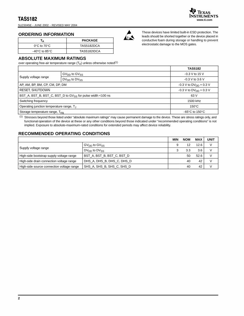
ORDERING INFORMATIONTA PACKAGE
0°C to 70°C TAS5182DCA
-40°C to 85°C TAS5182IDCA
These devices have limited built-in ESD protection. Theleads should be shorted together or the device placed inconductive foam during storage or handling to preventelectrostatic damage to the MOS gates.
ABSOLUTE MAXIMUM RATINGSover operating free-air temperature range (TA) unless otherwise noted(1)
TAS5182
Supply voltage rangeGVDD to GVSS -0.3 V to 15 V
Supply voltage rangeDVDD to DVSS -0.3 V to 3.6 V
AP, AM, BP, BM, CP, CM, DP, DM -0.3 V to DVDD + 0.3 V
RESET, SHUTDOWN -0.3 V to DVDD + 0.3 V
BST_A, BST_B, BST_C, BST_D to GVSS for pulse width <100 ns 63 V
Switching frequency 1500 kHz
Operating junction temperature range, TJ 150°C
Storage temperature range, Tstg -65°C to 150°C(1) Stresses beyond those listed under “absolute maximum ratings” may cause permanent damage to the device. These are stress ratings only, and
functional operation of the device at these or any other conditions beyond those indicated under “recommended operating conditions” is notimplied. Exposure to absolute-maximum-rated conditions for extended periods may affect device reliability.
RECOMMENDED OPERATING CONDITIONSMIN NOM MAX UNIT
Supply voltage rangeGVDD to GVSS 9 12 12.6 V
Supply voltage rangeDVDD to DVSS 3 3.3 3.6 V
High-side bootstrap supply voltage range BST_A, BST_B, BST_C, BST_D 50 52.6 V
High-side drain connection voltage range DHS_A, DHS_B, DHS_C, DHS_D 40 42 V
High-side source connection voltage range SHS_A, SHS_B, SHS_C, SHS_D 40 42 V
TAS5182SLES045E - JUNE 2002 - REVISED MAY 2004
www.ti.com
3
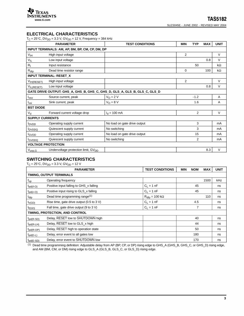
ELECTRICAL CHARACTERISTICS TC = 25°C, DVDD = 3.3 V, GVDD = 12 V, Frequency = 384 kHz
PARAMETER TEST CONDITIONS MIN TYP MAX UNIT
INPUT TERMINALS: AM, AP, BM, BP, CM, CP, DM, DP
VIH High input voltage 2 V
VIL Low input voltage 0.8 V
RI Input resistance 50 kΩ
Rdtp Dead time resistor range 0 100 kΩ
INPUT TERMINAL: RESET_X
VIH(RESET) High input voltage 2 V
VIL(RESET) Low input voltage 0.8 V
GATE DRIVE OUTPUT: GHS_A, GHS_B, GHS_C, GHS_D, GLS_A, GLS_B, GLS_C, GLS_D
Ioso Source current, peak VO = 2 V -1.2 A
Iosi Sink current, peak VO = 8 V 1.6 A
BST DIODE
Vd Forward current voltage drop Id = 100 mA 2 V
SUPPLY CURRENTS
IDVDD Operating supply current No load on gate drive output 3 mA
IDVDDQ Quiescent supply current No switching 3 mA
IGVDD Operating supply current No load on gate drive output 15 mA
IGVDDQ Quiescent supply current No switching 2 mA
VOLTAGE PROTECTION
Vuvp,G Undervoltage protection limit, GVDD 8.3 V
SWITCHING CHARACTERISTICS TC = 25°C, DVDD = 3.3 V, GVDD = 12 V
PARAMETER TEST CONDITIONS MIN NOM MAX UNIT
TIMING, OUTPUT TERMINALS
fop Operating frequency 1500 kHz
tpd(if-O) Positive input falling to GHS_x falling CL = 1 nF 45 ns
tpd(ir-O) Positive input rising to GLS_x falling CL = 1 nF 45 ns
tdtp Dead time programming range(1) Rdfp = 100 kΩ 110 ns
tr(GD) Rise time, gate drive output (0.5 to 3 V) CL = 1 nF 4.5 ns
tf(GD) Fall time, gate drive output (9 to 3 V) CL = 1 nF 7 ns
TIMING, PROTECTION, AND CONTROL
tpd(R-SD) Delay, RESET low to SHUTDOWN high 40 ns
tpd(R-LH) Delay, RESET low to GLS_x high 44 ns
tpd(R-OP) Delay, RESET high to operation state 50 ns
tpd(E-L) Delay, error event to all gates low 180 ns
tpd(E-SD) Delay, error event to SHUTDOWN low 170 ns(1) Dead time programming definition: Adjustable delay from AP (BP, CP, or DP) rising edge to GHS_A (GHS_B, GHS_C, or GHS_D) rising edge,
and AM (BM, CM, or DM) rising edge to GLS_A (GLS_B, GLS_C, or GLS_D) rising edge.
TAS5182SLES045E - JUNE 2002 - REVISED MAY 2004
www.ti.com
4
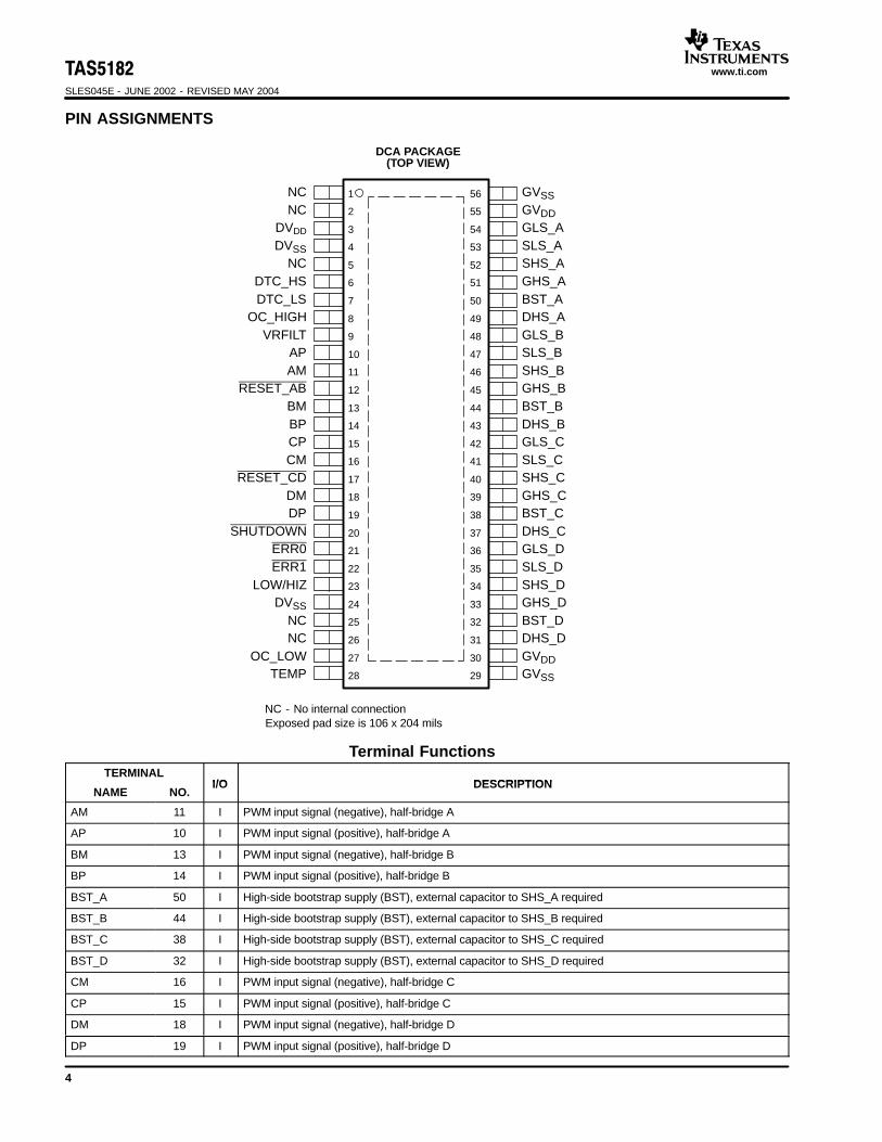
PIN ASSIGNMENTS
1
2
3
4
5
6
7
8
9
10
11
12
13
14
15
16
17
18
19
20
21
22
23
24
25
26
27
28
56
55
54
53
52
51
50
49
48
47
46
45
44
43
42
41
40
39
38
37
36
35
34
33
32
31
30
29
NCNC
DVDD
DVSSNC
DTC_HSDTC_LS
OC_HIGHVRFILT
APAM
RESET_ABBMBPCPCM
RESET_CDDMDP
SHUTDOWNERR0ERR1
LOW/HIZDVSS
NCNC
OC_LOWTEMP
GVSS
GVDDGLS_ASLS_ASHS_AGHS_ABST_ADHS_AGLS_BSLS_BSHS_BGHS_BBST_BDHS_BGLS_CSLS_CSHS_CGHS_CBST_CDHS_CGLS_DSLS_DSHS_DGHS_DBST_DDHS_DGVDDGVSS
DCA PACKAGE(TOP VIEW)
NC - No internal connectionExposed pad size is 106 x 204 mils
Terminal Functions TERMINAL
I/O DESCRIPTIONNAME NO.
I/O DESCRIPTION
AM 11 I PWM input signal (negative), half-bridge A
AP 10 I PWM input signal (positive), half-bridge A
BM 13 I PWM input signal (negative), half-bridge B
BP 14 I PWM input signal (positive), half-bridge B
BST_A 50 I High-side bootstrap supply (BST), external capacitor to SHS_A required
BST_B 44 I High-side bootstrap supply (BST), external capacitor to SHS_B required
BST_C 38 I High-side bootstrap supply (BST), external capacitor to SHS_C required
BST_D 32 I High-side bootstrap supply (BST), external capacitor to SHS_D required
CM 16 I PWM input signal (negative), half-bridge C
CP 15 I PWM input signal (positive), half-bridge C
DM 18 I PWM input signal (negative), half-bridge D
DP 19 I PWM input signal (positive), half-bridge D
TAS5182SLES045E - JUNE 2002 - REVISED MAY 2004
www.ti.com
5
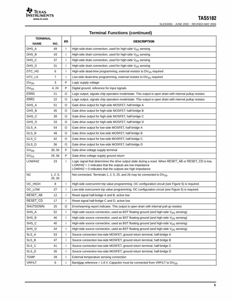
Terminal Functions (continued)TERMINAL
DESCRIPTIONI/ONAME
DESCRIPTIONI/ONO.
DHS_A 49 I High-side drain connection, used for high-side VDS sensing
DHS_B 43 I High-side drain connection, used for high-side VDS sensing
DHS_C 37 I High-side drain connection, used for high-side VDS sensing
DHS_D 31 I High-side drain connection, used for high-side VDS sensing
DTC_HS 6 I High-side dead-time programming, external resistor to DVSS required
DTC_LS 7 I Low-side dead-time programming, external resistor to DVSS required
DVDD 3 P Logic supply voltage
DVSS 4, 24 P Digital ground, reference for input signals
ERR0 21 O Logic output, signals chip operation mode/state. This output is open drain with internal pullup resistor.
ERR1 22 O Logic output, signals chip operation mode/state. This output is open drain with internal pullup resistor.
GHS_A 51 O Gate drive output for high-side MOSFET, half-bridge A
GHS_B 45 O Gate drive output for high-side MOSFET, half-bridge B
GHS_C 39 O Gate drive output for high-side MOSFET, half-bridge C
GHS_D 33 O Gate drive output for high-side MOSFET, half-bridge D
GLS_A 54 O Gate drive output for low-side MOSFET, half-bridge A
GLS_B 48 O Gate drive output for low-side MOSFET, half-bridge B
GLS_C 42 O Gate drive output for low-side MOSFET, half-bridge C
GLS_D 36 O Gate drive output for low-side MOSFET, half-bridge D
GVDD 30, 55 P Gate drive voltage supply terminal
GVSS 29, 56 P Gate drive voltage supply ground return
LOW/HIZ 23 I Logic signal that determines the drive output state during a reset. When RESET_AB or RESET_CD is low,LOW/HIZ = 1 indicates that the outputs are low impedanceLOW/HIZ = 0 indicates that the outputs are high impedance
NC 1, 2, 5,25, 26
Not connected. Terminals 1, 2, 5, 25, and 26 may be connected to DVSS.
OC_HIGH 8 I High-side overcurrent trip value programming. OC configuration circuit (see Figure 5) is required.
OC_LOW 27 I Low-side overcurrent trip value programming. OC configuration circuit (see Figure 5) is required.
RESET_AB 12 I Reset signal half-bridge A and B, active low
RESET_CD 17 I Reset signal half-bridge C and D, active low
SHUTDOWN 20 O Error/warning report indicator. This output is open drain with internal pull-up resistor.
SHS_A 52 I High-side source connection, used as BST floating ground (and high-side VDS sensing)
SHS_B 46 I High-side source connection, used as BST floating ground (and high-side VDS sensing)
SHS_C 40 I High-side source connection, used as BST floating ground (and high-side VDS sensing)
SHS_D 34 I High-side source connection, used as BST floating ground (and high-side VDS sensing)
SLS_A 53 I Source connection low-side MOSFET, ground return terminal, half-bridge A
SLS_B 47 I Source connection low-side MOSFET, ground return terminal, half-bridge B
SLS_C 41 I Source connection low-side MOSFET, ground return terminal, half-bridge C
SLS_D 35 I Source connection low-side MOSFET, ground return terminal, half-bridge D
TEMP 28 I External temperature sensing connection
VRFILT 9 I Bandgap reference = 1.8 V. Capacitor must be connected from VRFILT to DVSS.
TAS5182SLES045E - JUNE 2002 - REVISED MAY 2004
www.ti.com
6
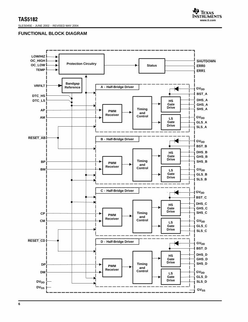
FUNCTIONAL BLOCK DIAGRAM
DP
DM
BST_D
DHS_DGHS_DSHS_D
GLS_DSLS_D
CP
CM
BST_C
DHS_CGHS_CSHS_C
GLS_C
SLS_C
BP
BM
BST_B
DHS_BGHS_B
SHS_B
GLS_B
SLS_B
PWMReceiver
Timingand
Control
HSGateDrive
LSGateDrive
AP
AM
BST_A
DHS_AGHS_ASHS_A
GLS_ASLS_A
Protection Circuitry Status
BandgapReferenceVRFILT
DTC_HSDTC_LS
OC_HIGH
TEMP
LOW/HIZ
A - Half-Bridge Driver
PWMReceiver
Timingand
Control
HSGateDrive
LSGateDrive
PWMReceiver
Timingand
Control
HSGateDrive
LSGateDrive
PWMReceiver
Timingand
Control
HSGateDrive
LSGateDrive
B - Half-Bridge Driver
C - Half-Bridge Driver
D - Half-Bridge Driver
RESET_AB
RESET_CD
SHUTDOWNERR0
ERR1
DVDD
DVSS
GVDD
GVSS
GVDD
GVDD
GVDD
GVDD
GVDD
GVDD
GVDD
OC_LOW
TAS5182SLES045E - JUNE 2002 - REVISED MAY 2004
www.ti.com
7
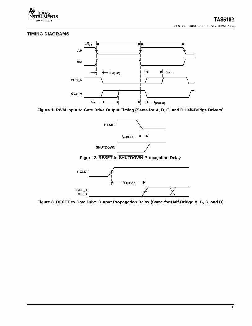
TIMING DIAGRAMS
AP
GHS_A
AM
GLS_A
1/fop
tpd(if-O) tdtp
tdtp tpd(ir-O)
Figure 1. PWM Input to Gate Drive Output Timing (Same for A, B, C, and D Half-Bridge Drivers)
tpd(R-SD)
RESET
SHUTDOWN
Figure 2. RESET to SHUTDOWN Propagation Delay
GHS_AGLS_A
tpd(R-OP)
RESET
Figure 3. RESET to Gate Drive Output Propagation Delay (Same for Half-Bridge A, B, C, and D)
TAS5182SLES045E - JUNE 2002 - REVISED MAY 2004
www.ti.com
8
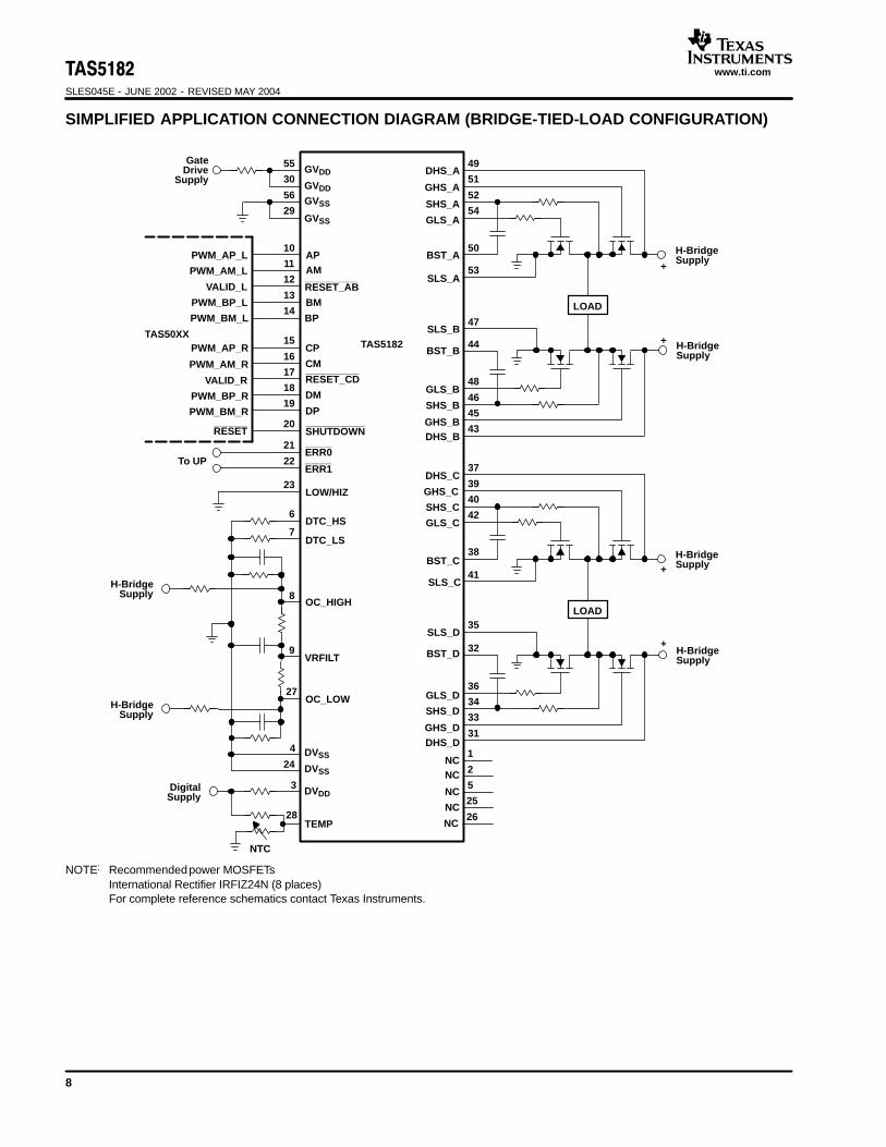
SIMPLIFIED APPLICATION CONNECTION DIAGRAM (BRIDGE-TIED-LOAD CONFIGURATION)
55
30
56
29
49
51
52
54
LOAD
48
46
45
43
37
39
40
42
LOAD
36
34
33
31
50
53
47
44
38
41
35
32
DigitalSupply
GateDrive
Supply
10
11
12
13
14
15
16
17
18
19
20
21
22
23
6
7
8
9
4
24
3
28
PWM_AP_L
PWM_AM_L
VALID_L
PWM_BP_L
PWM_BM_L
PWM_AP_R
PWM_AM_R
VALID_R
PWM_BP_R
PWM_BM_R
TAS50XX
+
+
+
+
H-BridgeSupply
H-BridgeSupply
To UP
1
2
5
25
26
NTC
27
DHS_A
GHS_A
SHS_A
GLS_A
DHS_BGHS_B
SHS_B
APAM
BM
BP
CP
CM
DM
DP
LOW/HIZ
DTC_HS
DTC_LS
OC_HIGH
VRFILT
TEMP
BST_A
SLS_A
GLS_B
SLS_B
BST_B
DHS_C
GHS_C
SHS_C
GLS_C
BST_C
SLS_C
SLS_D
BST_D
DHS_DGHS_D
SHS_D
GLS_D
TAS5182
DVDD
DVSS
DVSS
GVSS
GVDD
GVDD
GVSS
NCNC
NC
NC
NC
OC_LOWH-BridgeSupply
H-BridgeSupply
H-BridgeSupply
H-BridgeSupply
ERR0
RESET_AB
RESET_CD
ERR1
SHUTDOWNRESET
NOTE: Recommended power MOSFETsInternational Rectifier IRFIZ24N (8 places)For complete reference schematics contact Texas Instruments.
TAS5182
SLES045E - JUNE 2002 - REVISED MAY 2004
www.ti.com
9
FUNCTIONAL DESCRIPTION
Power Stage Protection
The TAS5182 device provides overcurrent,overtemperature, and undervoltage protection for theMOSFET power stage.
Overcurrent Protection (OCP)
To protect the power stage from damage due to highcurrents, a VDS sensing system is implemented in theTAS5182 device. Based on RDS(on) of the powerMOSFETs and the maximum allowed IDS, a voltagethreshold can be calculated which, when exceeded,triggers the protection latch, causing the SHUTDOWNterminal to go low. This voltage threshold is resistorprogrammable. See the Calculation of OvercurrentResistor Values section for more details.
Overtemperature Protection (OTP)
The TAS5182 device has a temperature protection systemthat uses an external negative temperature coefficient(NTC) resistor as a temperature sensor. See theOvertemperature Programming Circuit section forimplementation details.
Undervoltage Protection (UVP)
To protect the power output stage during start-up,shutdown, and other possible undervoltage conditions, theTAS5182 device provides power stage undervoltageprotection by driving its outputs low whenever GVDD isunder 7 V. With the TAS5182 outputs driven low, theMOSFETs go to a high-impedance state.
Control Terminals
The TAS5182 device provides input control terminals toreset each audio channel and also to control the electricalcharacteristics of the MOSFET output power stage.
Channel Reset
The reset function enables operation after power up,re-enables operation after an error event, and disables theMOSFET output stage switching during power down andmute. The falling edge of RESET_AB (left audio channel)or RESET_CD (right audio channel) causes the TAS5182device to reset. The rising edge of RESET_AB orRESET_CD causes the TAS5182 device to clear the errorlatch and resume normal operation.
MOSFET Output Reset Control
The LOW/HIZ control terminal selects whether theMOSFET output stage goes into a high-impedance (HI-Z)state or LOW-LOW state when RESET_AB orRESET_CD is enabled. In the high-impedance state, thelow-side and high-side MOSFETs are turned off causingno current flow through the MOSFETs. This effectivelydisconnects the load from the power supply rail. In theLOW-LOW state, the low-side MOSFETs are turned on,while the high-side MOSFETs are turned off. This causesa low or ground signal to be output to the load.
Status Terminals
The TAS5182 device provides output status terminals toreport overcurrent, overtemperature, and undervoltagewarnings and errors.
Shutdown Indicator
The SHUTDOWN terminal indicates an error event hasoccurred such as overcurrent, overtemperature, orundervoltage. The SHUTDOWN terminal is pulled highwhen RESET_AB or RESET_CD is asserted. ERR0 andERR1 terminals along with the SHUTDOWN terminalindicate the type of warnings and errors. Note thatSHUTDOWN is an open-drain signal. See Table 1 for afunctional description of these signals.
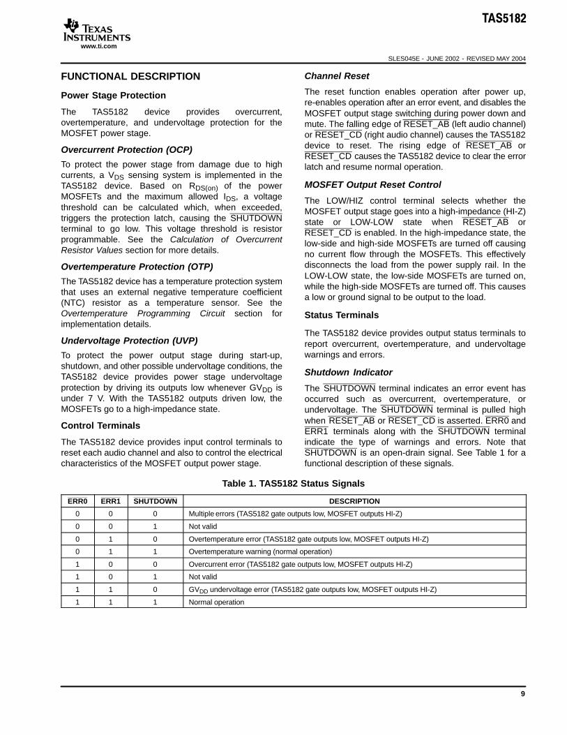
Table 1. TAS5182 Status Signals
ERR0 ERR1 SHUTDOWN DESCRIPTION
0 0 0 Multiple errors (TAS5182 gate outputs low, MOSFET outputs HI-Z)
0 0 1 Not valid
0 1 0 Overtemperature error (TAS5182 gate outputs low, MOSFET outputs HI-Z)
0 1 1 Overtemperature warning (normal operation)
1 0 0 Overcurrent error (TAS5182 gate outputs low, MOSFET outputs HI-Z)
1 0 1 Not valid
1 1 0 GVDD undervoltage error (TAS5182 gate outputs low, MOSFET outputs HI-Z)
1 1 1 Normal operation
TAS5182
SLES045E - JUNE 2002 - REVISED MAY 2004
www.ti.com
10
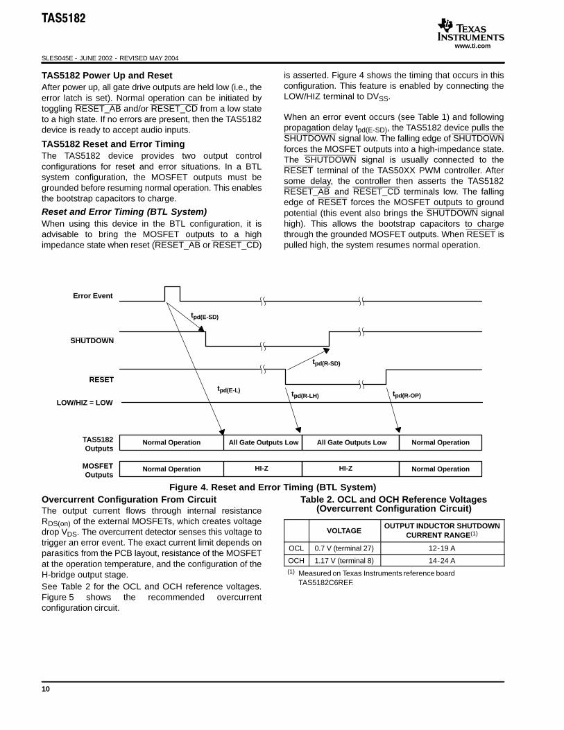
TAS5182 Power Up and ResetAfter power up, all gate drive outputs are held low (i.e., theerror latch is set). Normal operation can be initiated bytoggling RESET_AB and/or RESET_CD from a low stateto a high state. If no errors are present, then the TAS5182device is ready to accept audio inputs.
TAS5182 Reset and Error TimingThe TAS5182 device provides two output controlconfigurations for reset and error situations. In a BTLsystem configuration, the MOSFET outputs must begrounded before resuming normal operation. This enablesthe bootstrap capacitors to charge.
Reset and Error Timing (BTL System)When using this device in the BTL configuration, it isadvisable to bring the MOSFET outputs to a highimpedance state when reset (RESET_AB or RESET_CD)
is asserted. Figure 4 shows the timing that occurs in thisconfiguration. This feature is enabled by connecting theLOW/HIZ terminal to DVSS.
When an error event occurs (see Table 1) and followingpropagation delay tpd(E-SD), the TAS5182 device pulls theSHUTDOWN signal low. The falling edge of SHUTDOWNforces the MOSFET outputs into a high-impedance state.The SHUTDOWN signal is usually connected to theRESET terminal of the TAS50XX PWM controller. Aftersome delay, the controller then asserts the TAS5182RESET_AB and RESET_CD terminals low. The fallingedge of RESET forces the MOSFET outputs to groundpotential (this event also brings the SHUTDOWN signalhigh). This allows the bootstrap capacitors to chargethrough the grounded MOSFET outputs. When RESET ispulled high, the system resumes normal operation.
TAS5182Outputs
Error Event
LOW/HIZ = LOW
MOSFETOutputs
HI-Z HI-Z
SHUTDOWN
RESET
Normal Operation
Normal Operation
All Gate Outputs Low All Gate Outputs Low Normal Operation
Normal Operation
tpd(E-SD)
tpd(E-L) tpd(R-LH)
tpd(R-SD)
tpd(R-OP)
Figure 4. Reset and Error Timing (BTL System)Overcurrent Configuration From CircuitThe output current flows through internal resistanceRDS(on) of the external MOSFETs, which creates voltagedrop VDS. The overcurrent detector senses this voltage totrigger an error event. The exact current limit depends onparasitics from the PCB layout, resistance of the MOSFETat the operation temperature, and the configuration of theH-bridge output stage.See Table 2 for the OCL and OCH reference voltages.Figure 5 shows the recommended overcurrentconfiguration circuit.
Table 2. OCL and OCH Reference Voltages(Overcurrent Configuration Circuit)
VOLTAGEOUTPUT INDUCTOR SHUTDOWN
CURRENT RANGE(1)
OCL 0.7 V (terminal 27) 12-19 A
OCH 1.17 V (terminal 8) 14-24 A(1) Measured on Texas Instruments reference board
TAS5182C6REF.
TAS5182
SLES045E - JUNE 2002 - REVISED MAY 2004
www.ti.com
11
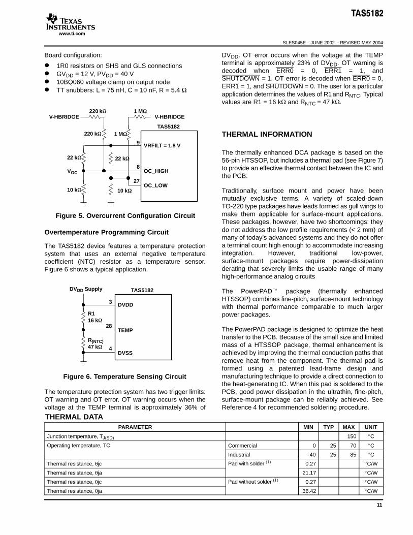
Board configuration:
1R0 resistors on SHS and GLS connections GVDD = 12 V, PVDD = 40 V 10BQ060 voltage clamp on output node TT snubbers: L = 75 nH, C = 10 nF, R = 5.4 Ω
OC_HIGH
VRFILT = 1.8 V
TAS5182
9
8VOC
Figure 5. Overcurrent Configuration Circuit
OC_LOW27
V-HBRIDGE V-HBRIDGE220 k
220 k
22 k 22 k
10 k 10 k
1 M
1 M
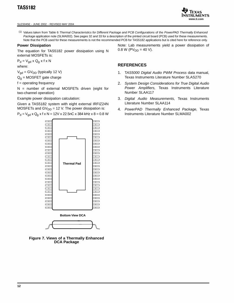
Overtemperature Programming Circuit
The TAS5182 device features a temperature protectionsystem that uses an external negative temperaturecoefficient (NTC) resistor as a temperature sensor.Figure 6 shows a typical application.
Figure 6. Temperature Sensing Circuit
TEMP
DVDD
TAS5182
3
28
DVSS4
R(NTC)47 k
DVDD Supply
R116 k
The temperature protection system has two trigger limits:OT warning and OT error. OT warning occurs when thevoltage at the TEMP terminal is approximately 36% of
DVDD. OT error occurs when the voltage at the TEMPterminal is approximately 23% of DVDD. OT warning isdecoded when ERR0 = 0, ERR1 = 1, andSHUTDOWN = 1. OT error is decoded when ERR0 = 0,ERR1 = 1, and SHUTDOWN = 0. The user for a particularapplication determines the values of R1 and RNTC. Typicalvalues are R1 = 16 kΩ and RNTC = 47 kΩ.
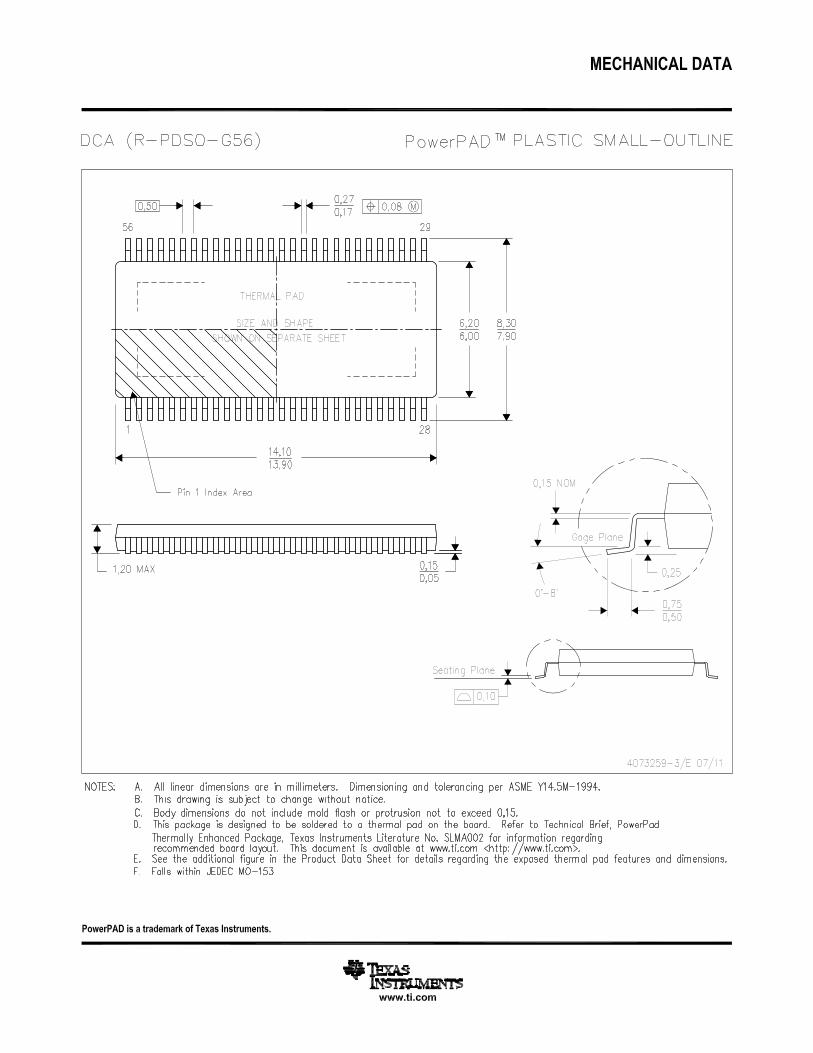
THERMAL INFORMATION
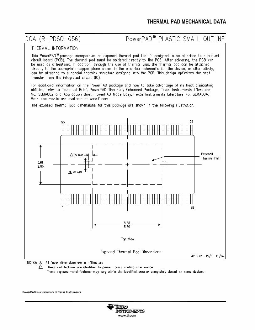
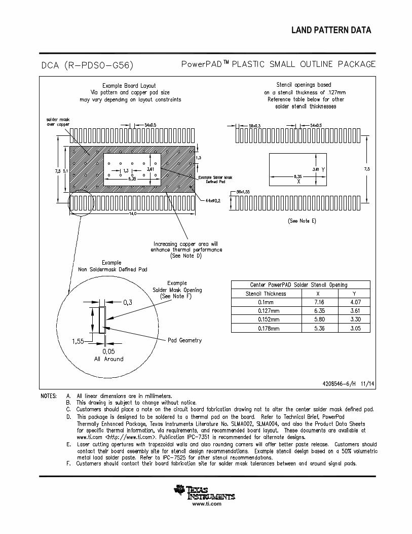
The thermally enhanced DCA package is based on the56-pin HTSSOP, but includes a thermal pad (see Figure 7)to provide an effective thermal contact between the IC andthe PCB.
Traditionally, surface mount and power have beenmutually exclusive terms. A variety of scaled-downTO-220 type packages have leads formed as gull wings tomake them applicable for surface-mount applications.These packages, however, have two shortcomings: theydo not address the low profile requirements (< 2 mm) ofmany of today’s advanced systems and they do not offera terminal count high enough to accommodate increasingintegration. However, traditional low-power,surface-mount packages require power-dissipationderating that severely limits the usable range of manyhigh-performance analog circuits
The PowerPAD package (thermally enhancedHTSSOP) combines fine-pitch, surface-mount technologywith thermal performance comparable to much largerpower packages.
The PowerPAD package is designed to optimize the heattransfer to the PCB. Because of the small size and limitedmass of a HTSSOP package, thermal enhancement isachieved by improving the thermal conduction paths thatremove heat from the component. The thermal pad isformed using a patented lead-frame design andmanufacturing technique to provide a direct connection tothe heat-generating IC. When this pad is soldered to thePCB, good power dissipation in the ultrathin, fine-pitch,surface-mount package can be reliably achieved. SeeReference 4 for recommended soldering procedure.
THERMAL DATAPARAMETER MIN TYP MAX UNIT
Junction temperature, TJ(SD) 150 C
Operating temperature, TC Commercial 0 25 70 Cp g p ,
Industrial -40 25 85 C
Thermal resistance, θjc Pad with solder (1) 0.27 C/W
Thermal resistance, θja 21.17 C/W
Thermal resistance, θjc Pad without solder (1) 0.27 C/W
Thermal resistance, θja 36.42 C/W
TAS5182
SLES045E - JUNE 2002 - REVISED MAY 2004
www.ti.com
12
(1) Values taken from Table 6 Thermal Characteristics for Different Package and PCB Configurations of the PowerPAD Thermally EnhancedPackage application note (SLMA002). See pages 32 and 33 for a description of the printed circuit board (PCB) used for these measurements.Note that the PCB used for these measurements is not the recommended PCB for TAS5182 applications but is cited here for reference only.
Power DissipationThe equation for TAS5182 power dissipation using Nexternal MOSFETs is:
Pd = Vgd x Qg x f x N
where:
Vgd = GVDD (typically 12 V)
Qg = MOSFET gate charge
f = operating frequency
N = number of external MOSFETs driven (eight fortwo-channel operation)
Example power dissipation calculation:
Given a TAS5182 system with eight external IRFIZ24NMOSFETs and GVDD = 12 V. The power dissipation is:
Pd = Vgd x Qg x f x N = 12V x 22.5nC x 384 kHz x 8 = 0.8 W
Note: Lab measurements yield a power dissipation of0.8 W (PVDD = 40 V).
REFERENCES
1. TAS5000 Digital Audio PWM Process data manual,Texas Instruments Literature Number SLAS270
2. System Design Considerations for True Digital AudioPower Amplifiers, Texas Instruments LiteratureNumber SLAA117
3. Digital Audio Measurements, Texas InstrumentsLiterature Number SLAA114
4. PowerPAD Thermally Enhanced Package, TexasInstruments Literature Number SLMA002
Bottom View DCA
Thermal Pad
Figure 7. Views of a Thermally EnhancedDCA Package
5
5
4
4
3
3
2
2
1
1
D D
C C
B B
A A
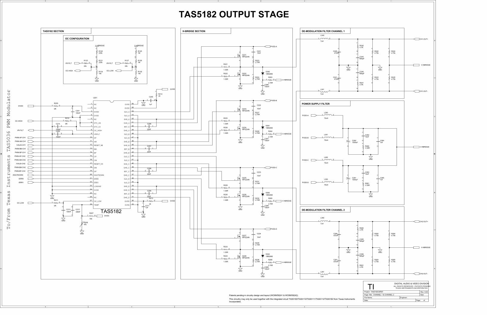
POWER SUPPLY FILTER
DE-MODULATION FILTER CHANNEL 1
DE-MODULATION FILTER CHANNEL 2
Patents pending in circuitry design and layout (WO99/59241 & WO99/59242).
This circuitry may only be used together with the integrated circuit TAS5100/TAS5110/TAS5111/TAS5112/TAS5182 from Texas InstrumentsIncorporated.
TAS5182 SECTION H-BRIDGE SECTION
TAS5182 OUTPUT STAGE
OC CONFIGURATION
To/From Texas Instruments TAS5036 PWM Modulator
6.00CHANNEL 1 & CHANNEL 2
TAS5182C6REF Rev:Page Title:
TI DIGITAL AUDIO & VIDEO DIVISIONALL RIGHTS RESERVED - PATENTS PENDING
TEXAS INSTRUMENTS INCORPORATED
Project:
File Name:Date:
Engineer:Page: of
Size:
GND
GND
GND
GND
GND
GND
GND
GND
GND
GND
GND
GND
GND
GND
GND
GND
GND
GND
V-HBRIDGE
GND
GND
GND
V-HBRIDGE
C26210nF
21
C208
22nF
2 1
C267100nF
21
C223
10nF
21
C2641nF
21
R2404.7R
12
C2601000uF
12
D26210BQ060
R205
0R
1 2
C241470nF
21
R2424.70k
12
R2272.70R
12
C245680pF
21
R2844.70k
12
R2352.70R
12
R225
1.00R
1 2
R2814.7R
12
C240470nF
21
R233
1.00R
1 2
R2242.70R
12
C202
100nF
21
Q226IRFIZ24N1
23
U201
TAS5182
1
2
3
4
5
6
7
8
9
10
11
12
13
14
15
16
18
19
20
21
22
23
24
25
26
27
28 29
30
31
32
17
56
55
54
53
52
51
50
49
48
47
46
45
44
43
42
41
40
39
38
37
36
35
34
33
NC
NC
DVDD
DVSS
NC
DTC_HS
DTC_LS
OC_HIGH
VRFILT
AP
AM
RESET_AB
BM
BP
CP
CM
DM
DP
SHUTDOWN
ERR0
ERR1
LOW/HIZ
DVSS
NC
NC
OC_LOW
TEMP GVSS
GVDD
DHS_D
BST_D
RESET_CD
GVSS
GVDD
GLS_A
SLS_A
SHS_A
GHS_A
BST_A
DHS_A
GLS_B
SLS_B
SHS_B
GHS_B
BST_B
DHS_B
GLS_C
SLS_C
SHS_C
GHS_C
BST_C
DHS_C
GLS_D
SLS_D
SHS_D
GHS_D
C280470nF
21
D26110BQ060
L240
7uH1 2
C212100nF
21
C246680pF
21
R266
2.70R
1 2
R264
2.70R
1 2
L281
7uH
12
L262
75nH
1 2
R265
2.70R
1 2R213
1R
1 2
R2804.7R
12
L261
75nH
1 2
C209
22nF
2 1
C2111uF
21
R2282.70R
12
R2613.30R
12
R2362.70R
12
R226
1.00R
1 2
C206
22nF
2 1
C266100nF
21
R234
1.00R
1 2
D26310BQ060
C286680pF
21
Q223IRFIZ24N1
23
R207
16k
1 2
L241
7uH
12
R2444.70k
12
R2854.70k
12
Q227IRFIZ24N1
23
R2121R
12
C22110nF
21
R2824.70k
12
C205
1uF
21
R221
1.00R
1 2
R2312.70R
12
R2603.30R
12
L260
75nH
1 2
R229
1.00R
1 2
C222
10nF
21
Q222IRFIZ24N1
23
C285680pF
21
C224
10nF
21
R2434.70k
12
C2611000uF
12
C268100nF
21
C214
100nF
21
R263
2.70R
1 2
C281470nF
21
C207
22nF
2 1
C213100nF
21
C201100nF
21
C26310nF
21
R210
0R
1 2
R2834.70k
12
Q221IRFIZ24N1
23
Q224IRFIZ24N1
23
D26010BQ060R222
1.00R
1 2
C2651nF
21
Q228IRFIZ24N1
23
R2322.70R
12
R2454.70k
12
R230
1.00R
1 2
R211
0R
1 2
Q225IRFIZ24N1
23
R2414.7R
12
L263
75nH
1 2
R2232.70R
12
L280
7uH1 2
R1261M
12
R1251M
12
R127
22k
1 2R123
22k
1 2
R12410k
12
R121220k
12
C269100nF
21
R12810k
12
R120220k
12
R20847k
21
V-HBRIDGE
/VALID-CH2
DVDD
/VALID-CH1
/ERR0
DVDD
/SHUTDOWN
/ERR1
PWM-BP-CH1
PWM-BM-CH1
PWM-AM-CH1
PWM-AP-CH1
PVDD-A
PVDD-A
PVDD-B
CH1-OUT+
CH1-OUT-
PWM-BP-CH2
PWM-BM-CH2
PWM-AM-CH2
PWM-AP-CH2
CH2-OUT+
CH2-OUT-
PVDD-D
PVDD-C
PVDD-B
PVDD-C
PVDD-D
GVDD
GVDD
V-HBRIDGE
V-HBRIDGE
OC-HIGH
OC-LOW
VR-FILT
V-HBRIDGE
V-HBRIDGE
V-HBRIDGE
V-HBRIDGE
OC-HIGH
VR-FILT VR-FILT
OC-LOW
PACKAGE OPTION ADDENDUM
www.ti.com 10-Jun-2014
Addendum-Page 1
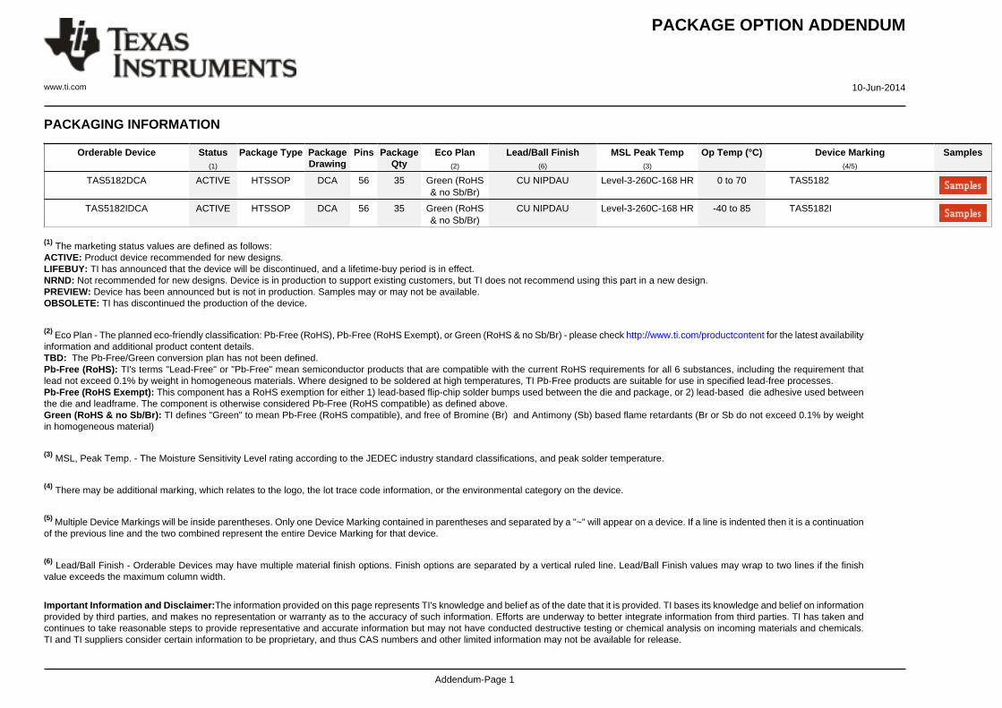
PACKAGING INFORMATION
Orderable Device Status(1)
Package Type PackageDrawing
Pins PackageQty
Eco Plan(2)
Lead/Ball Finish(6)
MSL Peak Temp(3)
Op Temp (°C) Device Marking(4/5)
Samples
TAS5182DCA ACTIVE HTSSOP DCA 56 35 Green (RoHS& no Sb/Br)
CU NIPDAU Level-3-260C-168 HR 0 to 70 TAS5182
TAS5182IDCA ACTIVE HTSSOP DCA 56 35 Green (RoHS& no Sb/Br)
CU NIPDAU Level-3-260C-168 HR -40 to 85 TAS5182I
(1) The marketing status values are defined as follows:ACTIVE: Product device recommended for new designs.LIFEBUY: TI has announced that the device will be discontinued, and a lifetime-buy period is in effect.NRND: Not recommended for new designs. Device is in production to support existing customers, but TI does not recommend using this part in a new design.PREVIEW: Device has been announced but is not in production. Samples may or may not be available.OBSOLETE: TI has discontinued the production of the device.
(2) Eco Plan - The planned eco-friendly classification: Pb-Free (RoHS), Pb-Free (RoHS Exempt), or Green (RoHS & no Sb/Br) - please check http://www.ti.com/productcontent for the latest availabilityinformation and additional product content details.TBD: The Pb-Free/Green conversion plan has not been defined.Pb-Free (RoHS): TI's terms "Lead-Free" or "Pb-Free" mean semiconductor products that are compatible with the current RoHS requirements for all 6 substances, including the requirement thatlead not exceed 0.1% by weight in homogeneous materials. Where designed to be soldered at high temperatures, TI Pb-Free products are suitable for use in specified lead-free processes.Pb-Free (RoHS Exempt): This component has a RoHS exemption for either 1) lead-based flip-chip solder bumps used between the die and package, or 2) lead-based die adhesive used betweenthe die and leadframe. The component is otherwise considered Pb-Free (RoHS compatible) as defined above.Green (RoHS & no Sb/Br): TI defines "Green" to mean Pb-Free (RoHS compatible), and free of Bromine (Br) and Antimony (Sb) based flame retardants (Br or Sb do not exceed 0.1% by weightin homogeneous material)
(3) MSL, Peak Temp. - The Moisture Sensitivity Level rating according to the JEDEC industry standard classifications, and peak solder temperature.
(4) There may be additional marking, which relates to the logo, the lot trace code information, or the environmental category on the device.
(5) Multiple Device Markings will be inside parentheses. Only one Device Marking contained in parentheses and separated by a "~" will appear on a device. If a line is indented then it is a continuationof the previous line and the two combined represent the entire Device Marking for that device.
(6) Lead/Ball Finish - Orderable Devices may have multiple material finish options. Finish options are separated by a vertical ruled line. Lead/Ball Finish values may wrap to two lines if the finishvalue exceeds the maximum column width.
Important Information and Disclaimer:The information provided on this page represents TI's knowledge and belief as of the date that it is provided. TI bases its knowledge and belief on informationprovided by third parties, and makes no representation or warranty as to the accuracy of such information. Efforts are underway to better integrate information from third parties. TI has taken andcontinues to take reasonable steps to provide representative and accurate information but may not have conducted destructive testing or chemical analysis on incoming materials and chemicals.TI and TI suppliers consider certain information to be proprietary, and thus CAS numbers and other limited information may not be available for release.

PACKAGE OPTION ADDENDUM
www.ti.com 10-Jun-2014
Addendum-Page 2
In no event shall TI's liability arising out of such information exceed the total purchase price of the TI part(s) at issue in this document sold by TI to Customer on an annual basis.
IMPORTANT NOTICETexas Instruments Incorporated and its subsidiaries (TI) reserve the right to make corrections, enhancements, improvements and otherchanges to its semiconductor products and services per JESD46, latest issue, and to discontinue any product or service per JESD48, latestissue. Buyers should obtain the latest relevant information before placing orders and should verify that such information is current andcomplete. All semiconductor products (also referred to herein as “components”) are sold subject to TI’s terms and conditions of salesupplied at the time of order acknowledgment.TI warrants performance of its components to the specifications applicable at the time of sale, in accordance with the warranty in TI’s termsand conditions of sale of semiconductor products. Testing and other quality control techniques are used to the extent TI deems necessaryto support this warranty. Except where mandated by applicable law, testing of all parameters of each component is not necessarilyperformed.TI assumes no liability for applications assistance or the design of Buyers’ products. Buyers are responsible for their products andapplications using TI components. To minimize the risks associated with Buyers’ products and applications, Buyers should provideadequate design and operating safeguards.TI does not warrant or represent that any license, either express or implied, is granted under any patent right, copyright, mask work right, orother intellectual property right relating to any combination, machine, or process in which TI components or services are used. Informationpublished by TI regarding third-party products or services does not constitute a license to use such products or services or a warranty orendorsement thereof. Use of such information may require a license from a third party under the patents or other intellectual property of thethird party, or a license from TI under the patents or other intellectual property of TI.Reproduction of significant portions of TI information in TI data books or data sheets is permissible only if reproduction is without alterationand is accompanied by all associated warranties, conditions, limitations, and notices. TI is not responsible or liable for such altereddocumentation. Information of third parties may be subject to additional restrictions.Resale of TI components or services with statements different from or beyond the parameters stated by TI for that component or servicevoids all express and any implied warranties for the associated TI component or service and is an unfair and deceptive business practice.TI is not responsible or liable for any such statements.Buyer acknowledges and agrees that it is solely responsible for compliance with all legal, regulatory and safety-related requirementsconcerning its products, and any use of TI components in its applications, notwithstanding any applications-related information or supportthat may be provided by TI. Buyer represents and agrees that it has all the necessary expertise to create and implement safeguards whichanticipate dangerous consequences of failures, monitor failures and their consequences, lessen the likelihood of failures that might causeharm and take appropriate remedial actions. Buyer will fully indemnify TI and its representatives against any damages arising out of the useof any TI components in safety-critical applications.In some cases, TI components may be promoted specifically to facilitate safety-related applications. With such components, TI’s goal is tohelp enable customers to design and create their own end-product solutions that meet applicable functional safety standards andrequirements. Nonetheless, such components are subject to these terms.No TI components are authorized for use in FDA Class III (or similar life-critical medical equipment) unless authorized officers of the partieshave executed a special agreement specifically governing such use.Only those TI components which TI has specifically designated as military grade or “enhanced plastic” are designed and intended for use inmilitary/aerospace applications or environments. Buyer acknowledges and agrees that any military or aerospace use of TI componentswhich have not been so designated is solely at the Buyer's risk, and that Buyer is solely responsible for compliance with all legal andregulatory requirements in connection with such use.TI has specifically designated certain components as meeting ISO/TS16949 requirements, mainly for automotive use. In any case of use ofnon-designated products, TI will not be responsible for any failure to meet ISO/TS16949.Products ApplicationsAudio www.ti.com/audio Automotive and Transportation www.ti.com/automotiveAmplifiers amplifier.ti.com Communications and Telecom www.ti.com/communicationsData Converters dataconverter.ti.com Computers and Peripherals www.ti.com/computersDLP® Products www.dlp.com Consumer Electronics www.ti.com/consumer-appsDSP dsp.ti.com Energy and Lighting www.ti.com/energyClocks and Timers www.ti.com/clocks Industrial www.ti.com/industrialInterface interface.ti.com Medical www.ti.com/medicalLogic logic.ti.com Security www.ti.com/securityPower Mgmt power.ti.com Space, Avionics and Defense www.ti.com/space-avionics-defenseMicrocontrollers microcontroller.ti.com Video and Imaging www.ti.com/videoRFID www.ti-rfid.comOMAP Applications Processors www.ti.com/omap TI E2E Community e2e.ti.comWireless Connectivity www.ti.com/wirelessconnectivity
Mailing Address: Texas Instruments, Post Office Box 655303, Dallas, Texas 75265Copyright © 2014, Texas Instruments Incorporated