Tao Wang, Huili Liang,* Zuyin Han, Yanxin Sui, and Zengxia ...
7
2000945 (1 of 7) © 2021 Wiley-VCH GmbH www.advmattechnol.de FULL PAPER Integrated Flexible Ga 2 O 3 Deep UV Photodetectors Powered by Environmental Electromagnetic Radiation Energy Tao Wang, Huili Liang,* Zuyin Han, Yanxin Sui, and Zengxia Mei* DOI: 10.1002/admt.202000945 gallium oxide (β-Ga 2 O 3 ), amorphous Ga 2 O 3 (a-Ga 2 O 3 ) has captured growing attention for its superior compatibility with low-temperature fabrication process and prospects in wearable and flexible electronics. [7] It also gained momentum in other core technology such as phototran- sistors, [8] X-ray detectors, [16] and gas sen- sors. [17] In many application scenarios of wearable electronics, however, the bulky power supply component greatly limits user experience. Therefore, self-powered UV PDs are more preferred. Much of the research on self-powered Ga 2 O 3 UV PDs is based on crystal Ga 2 O 3 , utilizing the photovoltaic effect inside the heterojunctions or Schottky junc- tions. [18–23] Beside the common problem of high preparation temperature, perfor- mance of this kind of PDs also strongly depends on the interface quality or Schottky barrier height, which are extremely restricted by the crystal quality and lat- tice matching between two different materials, or the differ- ence between metal work function and electron affinity of Ga 2 O 3 . [24] That gives rise to a low photoresponsivity, usually below the level of ≈10 −2 A W −1 , as a major obstacle to their practical applications considering high sensitivity is one of the bases for PDs to capture weak signals. [25] One solution to the existing issue is finding a new power source. It is well-known that the human body is a kind of dielectric medium that can couple with electromagnetic field of certain frequency, the 50 Hz electromagnetic field from China standard electric grid, for instance. Accordingly, an induced current will be generated inside human body. [26–28] Such electrical signals are intuitively considered as interference in electrical systems which need to be shielded via special designs. In this work, however, the weak energy is subtly collected and applied as a power source to drive the a-Ga 2 O 3 PD. Specifically, the self-powered UV photodetection system is organized with an integration of a receiving electrode, a full-wave rectifier, and an a-Ga 2 O 3 UV PD with metal– semiconductor–metal (MSM) structure. The receiving elec- trode is used to harvest the energy coming from the coupling between human body and environmental electromagnetic radiation via its contact with human hand, and the downstream full-wave rectifier composed of four thin film diodes (TFDs) converts the alternating current (AC) into direct current (DC) signal. [29,30] Note that these diodes show a high rectification This work reports an integrated flexible deep ultraviolet (UV) photodetection system hosting an amorphous Ga 2 O 3 (a-Ga 2 O 3 ) photodetector (PD) and an energy harvesting component including a receiving electrode and a full-wave rectifier. An alternating signal is induced by the coupling of human body with environmental electromagnetic radiation through human hand’s contact with the receiving electrode. The signal is subsequently converted into direct current (DC) by the rectifier which is composed of four thin-film diodes with high rectification ratio (≈10 6 ) and fast response time (rising time ≈240 µs and falling time ≈680 µs). Driven by the DC output, the a-Ga 2 O 3 PD achieves a photoresponsivity of 0.10 A W −1 and a detectivity of 2.24 × 10 11 Jones under 254 nm UV illumination. The integrated flexible a-Ga 2 O 3 UV PD manifests a repeatable and pleasurable response behavior with a bending radius of 15 mm, providing a new paradigm for utilizing the environmental energy as the power source in wearable electronics. T. Wang, Prof. H. Liang, Z. Han, Y. Sui, Prof. Z. Mei Key Laboratory for Renewable Energy Beijing Key Laboratory for New Energy Materials and Devices Institute of Physics Chinese Academy of Sciences Beijing 100190, China E-mail: [email protected]; [email protected] T. Wang, Prof. H. Liang, Z. Han, Y. Sui, Prof. Z. Mei Songshan Lake Materials Laboratory Dongguan, Guangdong 523808, China T. Wang, Z. Han, Y. Sui School of Physical Sciences University of Chinese Academy of Sciences Beijing 100049, China The ORCID identification number(s) for the author(s) of this article can be found under https://doi.org/10.1002/admt.202000945. 1. Introduction Deep ultraviolet (UV) photodetectors (PDs) have broad appli- cations including air/water purification, flame/engine con- trol, space communication, and so on. A host of materials like MgZnO, [1–3] AlGaN, [4,5] diamond, [6] and Ga 2 O 3 [7–13] have been extensively investigated to accomplish the challenging task. Among them, Ga 2 O 3 is considered as an ideal candidate owing to the merits of ultrawide direct bandgap (≈4.9 eV) and high absorption coefficient (>10 5 cm −1 near band edge) with no need of tricky alloying work. [14,15] Apart from monoclinic Adv. Mater. Technol. 2021, 6, 2000945
Transcript of Tao Wang, Huili Liang,* Zuyin Han, Yanxin Sui, and Zengxia ...
2000945 (1 of 7) © 2021 Wiley-VCH GmbH
www.advmattechnol.de
Full PaPer
Integrated Flexible Ga2O3 Deep UV Photodetectors Powered by Environmental Electromagnetic Radiation Energy
Tao Wang, Huili Liang,* Zuyin Han, Yanxin Sui, and Zengxia Mei*
DOI: 10.1002/admt.202000945
gallium oxide (β-Ga2O3), amorphous Ga2O3 (a-Ga2O3) has captured growing attention for its superior compatibility with low-temperature fabrication process and prospects in wearable and flexible electronics.[7] It also gained momentum in other core technology such as phototran-sistors,[8] X-ray detectors,[16] and gas sen-sors.[17] In many application scenarios of wearable electronics, however, the bulky power supply component greatly limits user experience. Therefore, self-powered UV PDs are more preferred.
Much of the research on self-powered Ga2O3 UV PDs is based on crystal Ga2O3, utilizing the photovoltaic effect inside the heterojunctions or Schottky junc-tions.[18–23] Beside the common problem of high preparation temperature, perfor-mance of this kind of PDs also strongly
depends on the interface quality or Schottky barrier height, which are extremely restricted by the crystal quality and lat-tice matching between two different materials, or the differ-ence between metal work function and electron affinity of Ga2O3.[24] That gives rise to a low photoresponsivity, usually below the level of ≈10−2 A W−1, as a major obstacle to their practical applications considering high sensitivity is one of the bases for PDs to capture weak signals.[25] One solution to the existing issue is finding a new power source. It is well-known that the human body is a kind of dielectric medium that can couple with electromagnetic field of certain frequency, the 50 Hz electromagnetic field from China standard electric grid, for instance. Accordingly, an induced current will be generated inside human body.[26–28] Such electrical signals are intuitively considered as interference in electrical systems which need to be shielded via special designs. In this work, however, the weak energy is subtly collected and applied as a power source to drive the a-Ga2O3 PD.
Specifically, the self-powered UV photodetection system is organized with an integration of a receiving electrode, a full-wave rectifier, and an a-Ga2O3 UV PD with metal–semiconductor–metal (MSM) structure. The receiving elec-trode is used to harvest the energy coming from the coupling between human body and environmental electromagnetic radiation via its contact with human hand, and the downstream full-wave rectifier composed of four thin film diodes (TFDs) converts the alternating current (AC) into direct current (DC) signal.[29,30] Note that these diodes show a high rectification
This work reports an integrated flexible deep ultraviolet (UV) photodetection system hosting an amorphous Ga2O3 (a-Ga2O3) photodetector (PD) and an energy harvesting component including a receiving electrode and a full-wave rectifier. An alternating signal is induced by the coupling of human body with environmental electromagnetic radiation through human hand’s contact with the receiving electrode. The signal is subsequently converted into direct current (DC) by the rectifier which is composed of four thin-film diodes with high rectification ratio (≈106) and fast response time (rising time ≈240 µs and falling time ≈680 µs). Driven by the DC output, the a-Ga2O3 PD achieves a photoresponsivity of 0.10 A W−1 and a detectivity of 2.24 × 10¹¹ Jones under 254 nm UV illumination. The integrated flexible a-Ga2O3 UV PD manifests a repeatable and pleasurable response behavior with a bending radius of 15 mm, providing a new paradigm for utilizing the environmental energy as the power source in wearable electronics.
T. Wang, Prof. H. Liang, Z. Han, Y. Sui, Prof. Z. MeiKey Laboratory for Renewable EnergyBeijing Key Laboratory for New Energy Materials and DevicesInstitute of PhysicsChinese Academy of SciencesBeijing 100190, ChinaE-mail: [email protected]; [email protected]. Wang, Prof. H. Liang, Z. Han, Y. Sui, Prof. Z. MeiSongshan Lake Materials LaboratoryDongguan, Guangdong 523808, ChinaT. Wang, Z. Han, Y. SuiSchool of Physical SciencesUniversity of Chinese Academy of SciencesBeijing 100049, China
The ORCID identification number(s) for the author(s) of this article can be found under https://doi.org/10.1002/admt.202000945.
1. Introduction
Deep ultraviolet (UV) photodetectors (PDs) have broad appli-cations including air/water purification, flame/engine con-trol, space communication, and so on. A host of materials like MgZnO,[1–3] AlGaN,[4,5] diamond,[6] and Ga2O3
[7–13] have been extensively investigated to accomplish the challenging task. Among them, Ga2O3 is considered as an ideal candidate owing to the merits of ultrawide direct bandgap (≈4.9 eV) and high absorption coefficient (>105 cm−1 near band edge) with no need of tricky alloying work.[14,15] Apart from monoclinic
Adv. Mater. Technol. 2021, 6, 2000945
www.advancedsciencenews.com
© 2021 Wiley-VCH GmbH2000945 (2 of 7)
www.advmattechnol.de
ratio (Rr) of ≈106 as well as fast rising time of 240 µs and falling time of 680 µs. After rectification, the collected energy is uti-lized to power the a-Ga2O3 UV PD with no need of any external bias, exhibiting a decent UV detection performance with a light-to-dark ratio of 8.31, a responsivity of 0.10 A W−1, and a detectivity of 2.24 × 10¹¹ Jones under 254 nm UV illumination.
2. Results and Discussion
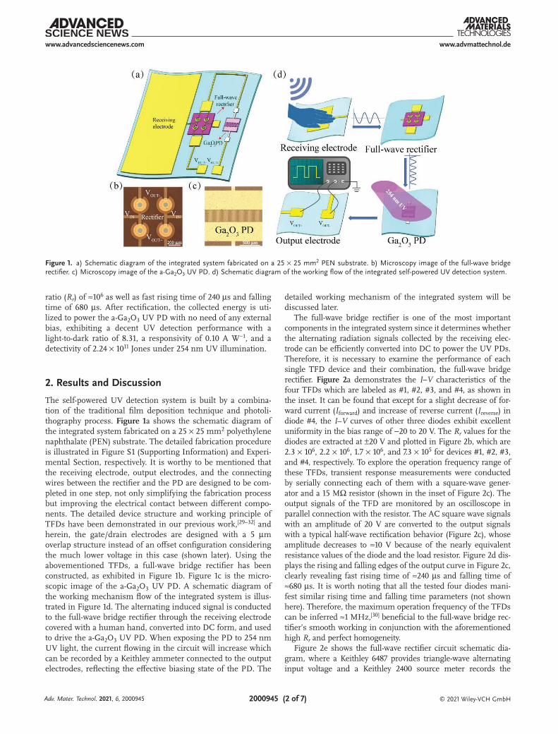
The self-powered UV detection system is built by a combina-tion of the traditional film deposition technique and photoli-thography process. Figure 1a shows the schematic diagram of the integrated system fabricated on a 25 × 25 mm2 polyethylene naphthalate (PEN) substrate. The detailed fabrication procedure is illustrated in Figure S1 (Supporting Information) and Experi-mental Section, respectively. It is worthy to be mentioned that the receiving electrode, output electrodes, and the connecting wires between the rectifier and the PD are designed to be com-pleted in one step, not only simplifying the fabrication process but improving the electrical contact between different compo-nents. The detailed device structure and working principle of TFDs have been demonstrated in our previous work,[29–32] and herein, the gate/drain electrodes are designed with a 5 µm overlap structure instead of an offset configuration considering the much lower voltage in this case (shown later). Using the abovementioned TFDs, a full-wave bridge rectifier has been constructed, as exhibited in Figure 1b. Figure 1c is the micro-scopic image of the a-Ga2O3 UV PD. A schematic diagram of the working mechanism flow of the integrated system is illus-trated in Figure 1d. The alternating induced signal is conducted to the full-wave bridge rectifier through the receiving electrode covered with a human hand, converted into DC form, and used to drive the a-Ga2O3 UV PD. When exposing the PD to 254 nm UV light, the current flowing in the circuit will increase which can be recorded by a Keithley ammeter connected to the output electrodes, reflecting the effective biasing state of the PD. The
detailed working mechanism of the integrated system will be discussed later.
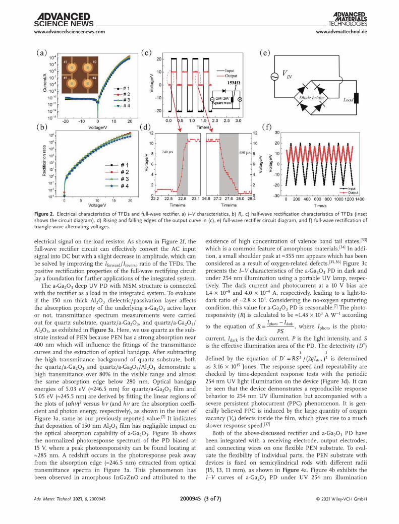
The full-wave bridge rectifier is one of the most important components in the integrated system since it determines whether the alternating radiation signals collected by the receiving elec-trode can be efficiently converted into DC to power the UV PDs. Therefore, it is necessary to examine the performance of each single TFD device and their combination, the full-wave bridge rectifier. Figure 2a demonstrates the I–V characteristics of the four TFDs which are labeled as #1, #2, #3, and #4, as shown in the inset. It can be found that except for a slight decrease of for-ward current (Iforward) and increase of reverse current (Ireverse) in diode #4, the I–V curves of other three diodes exhibit excellent uniformity in the bias range of −20 to 20 V. The Rr values for the diodes are extracted at ±20 V and plotted in Figure 2b, which are 2.3 × 10⁶, 2.2 × 10⁶, 1.7 × 10⁶, and 7.3 × 10⁵ for devices #1, #2, #3, and #4, respectively. To explore the operation frequency range of these TFDs, transient response measurements were conducted by serially connecting each of them with a square-wave gener-ator and a 15 MΩ resistor (shown in the inset of Figure 2c). The output signals of the TFD are monitored by an oscilloscope in parallel connection with the resistor. The AC square wave signals with an amplitude of 20 V are converted to the output signals with a typical half-wave rectification behavior (Figure 2c), whose amplitude decreases to ≈10 V because of the nearly equivalent resistance values of the diode and the load resistor. Figure 2d dis-plays the rising and falling edges of the output curve in Figure 2c, clearly revealing fast rising time of ≈240 µs and falling time of ≈680 µs. It is worth noting that all the tested four diodes mani-fest similar rising time and falling time parameters (not shown here). Therefore, the maximum operation frequency of the TFDs can be inferred ≈1 MHz,[30] beneficial to the full-wave bridge rec-tifier’s smooth working in conjunction with the aforementioned high Rr and perfect homogeneity.
Figure 2e shows the full-wave rectifier circuit schematic dia-gram, where a Keithley 6487 provides triangle-wave alternating input voltage and a Keithley 2400 source meter records the
Figure 1. a) Schematic diagram of the integrated system fabricated on a 25 × 25 mm2 PEN substrate. b) Microscopy image of the full-wave bridge rectifier. c) Microscopy image of the a-Ga2O3 UV PD. d) Schematic diagram of the working flow of the integrated self-powered UV detection system.
Adv. Mater. Technol. 2021, 6, 2000945
www.advancedsciencenews.com
© 2021 Wiley-VCH GmbH2000945 (3 of 7)
www.advmattechnol.de
electrical signal on the load resistor. As shown in Figure 2f, the full-wave rectifier circuit can effectively convert the AC input signal into DC but with a slight decrease in amplitude, which can be solved by improving the Iforward/Ireverse ratio of the TFDs. The positive rectification properties of the full-wave rectifying circuit lay a foundation for further applications of the integrated system.
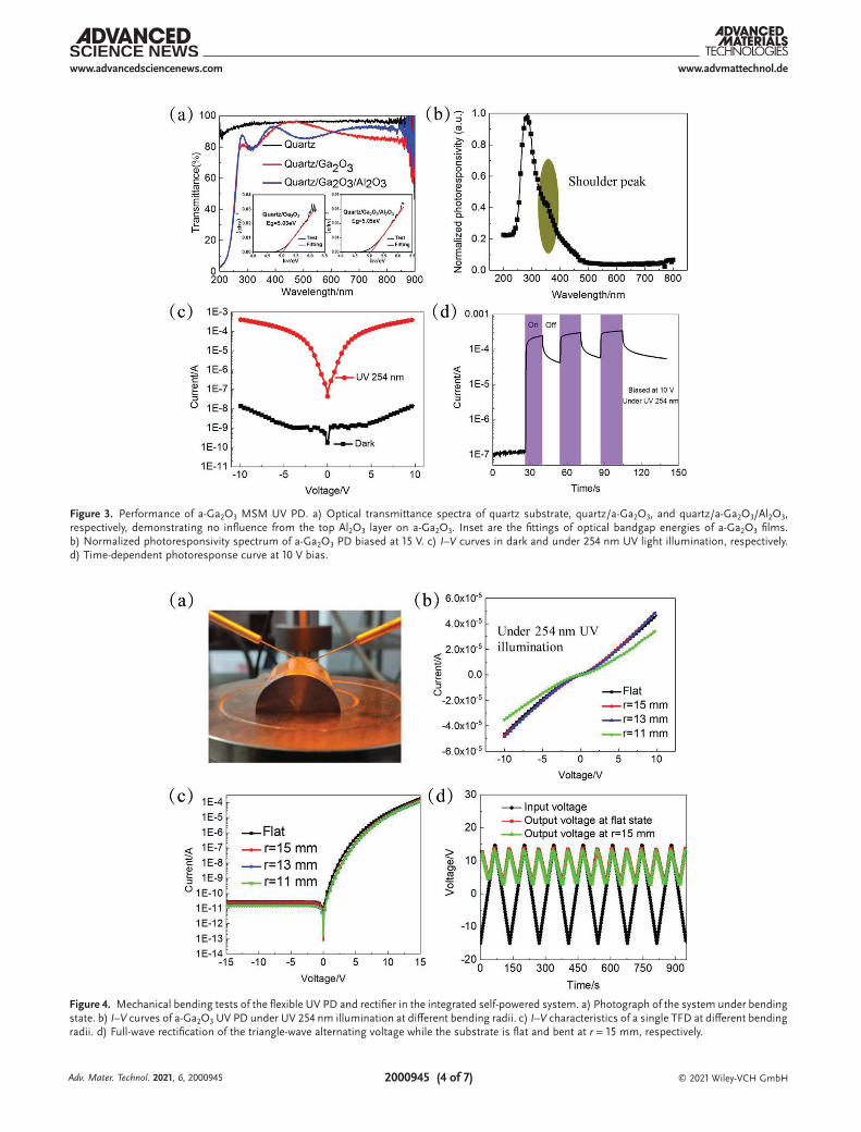
The a-Ga2O3 deep UV PD with MSM structure is connected with the rectifier as a load in the integrated system. To evaluate if the 150 nm thick Al2O3 dielectric/passivation layer affects the absorption property of the underlying a-Ga2O3 active layer or not, transmittance spectrum measurements were carried out for quartz substrate, quartz/a-Ga2O3, and quartz/a-Ga2O3/Al2O3, as exhibited in Figure 3a. Here, we use quartz as the sub-strate instead of PEN because PEN has a strong absorption near 400 nm which will influence the fittings of the transmittance curves and the extraction of optical bandgap. After subtracting the high transmittance background of quartz substrate, both the quartz/a-Ga2O3 and quartz/a-Ga2O3/Al2O3 demonstrate a high transmittance over 80% in the visible range and almost the same absorption edge below 280 nm. Optical bandgap energies of 5.03 eV (≈246.5 nm) for quartz/a-Ga2O3 film and 5.05 eV (≈245.5 nm) are derived by fitting the linear regions of the plots of (αhν)2 versus hν (and hν are the absorption coeffi-cient and photon energy, respectively), as shown in the inset of Figure 3a, same as our previously reported value.[7] It indicates that deposition of 150 nm Al2O3 film has negligible impact on the optical absorption capability of a-Ga2O3. Figure 3b shows the normalized photoresponse spectrum of the PD biased at 15 V, where a peak photoresponsivity can be found locating at ≈285 nm. A redshift occurs in the photoresponse peak away from the absorption edge (≈246.5 nm) extracted from optical transmittance spectra in Figure 3a. This phenomenon has been observed in amorphous InGaZnO and attributed to the
existence of high concentration of valence band tail states,[33] which is a common feature of amorphous materials.[34] In addi-tion, a small shoulder peak at ≈355 nm appears which has been considered as a result of oxygen-related defects.[35,36] Figure 3c presents the I–V characteristics of the a-Ga2O3 PD in dark and under 254 nm illumination using a portable UV lamp, respec-tively. The dark current and photocurrent at a 10 V bias are 1.4 × 10⁻⁸ and 4.0 × 10⁻⁴ A, respectively, leading to a light-to-dark ratio of ≈2.8 × 10⁴. Considering the no-oxygen sputtering condition, this value for a-Ga2O3 PD is reasonable.[7] The photo-responsivity (R) is calculated to be ≈1.43 × 10³ A W−1 according
to the equation of RI I
PSphoto dark=
−, where Iphoto is the photo-
current, Idark is the dark current, P is the light intensity, and S is the effective illumination area of the PD. The detectivity (D*)
defined by the equation of D RS qI/(2 )12
dark
12=∗ is determined
as 3.16 × 10¹⁵ Jones. The response speed and repeatability are checked by time-dependent response tests with the periodic 254 nm UV light illumination on the device (Figure 3d). It can be seen that the device demonstrates a reproducible response behavior to 254 nm UV illumination but accompanied with a severe persistent photocurrent (PPC) phenomenon. It is gen-erally believed PPC is induced by the large quantity of oxygen vacancy (Vo) defects inside the film, which gives rise to a much slower response speed.[37]
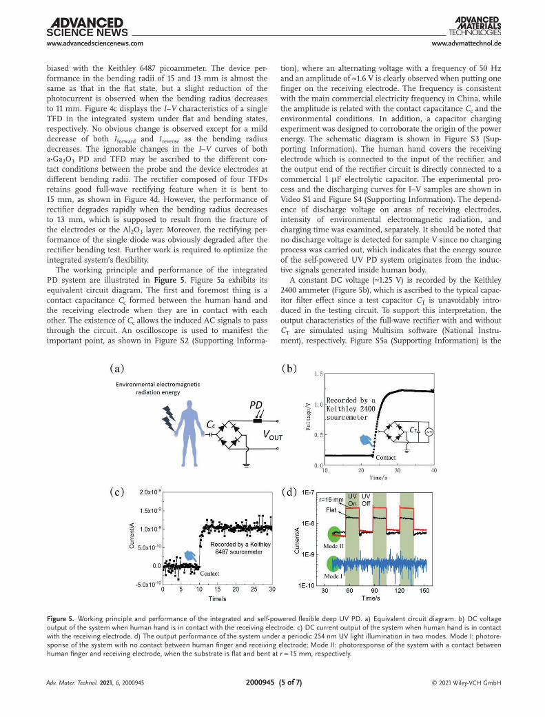
Both of the above-discussed rectifier and a-Ga2O3 PD have been integrated with a receiving electrode, output electrodes, and connecting wires on one flexible PEN substrate. To eval-uate the flexibility of individual parts, the PEN substrate with devices is fixed on semicylindrical rods with different radii (15, 13, 11 mm), as shown in Figure 4a. Figure 4b exhibits the I–V curves of a-Ga2O3 PD under UV 254 nm illumination
Figure 2. Electrical characteristics of TFDs and full-wave rectifier. a) I–V characteristics, b) Rr, c) half-wave rectification characteristics of TFDs (inset shows the circuit diagram). d) Rising and falling edges of the output curve in (c), e) full-wave rectifier circuit diagram, and f) full-wave rectification of triangle-wave alternating voltages.
Adv. Mater. Technol. 2021, 6, 2000945
www.advancedsciencenews.com
© 2021 Wiley-VCH GmbH2000945 (4 of 7)
www.advmattechnol.de
Figure 4. Mechanical bending tests of the flexible UV PD and rectifier in the integrated self-powered system. a) Photograph of the system under bending state. b) I–V curves of a-Ga2O3 UV PD under UV 254 nm illumination at different bending radii. c) I–V characteristics of a single TFD at different bending radii. d) Full-wave rectification of the triangle-wave alternating voltage while the substrate is flat and bent at r = 15 mm, respectively.
Figure 3. Performance of a-Ga2O3 MSM UV PD. a) Optical transmittance spectra of quartz substrate, quartz/a-Ga2O3, and quartz/a-Ga2O3/Al2O3, respectively, demonstrating no influence from the top Al2O3 layer on a-Ga2O3. Inset are the fittings of optical bandgap energies of a-Ga2O3 films. b) Normalized photoresponsivity spectrum of a-Ga2O3 PD biased at 15 V. c) I–V curves in dark and under 254 nm UV light illumination, respectively. d) Time-dependent photoresponse curve at 10 V bias.
Adv. Mater. Technol. 2021, 6, 2000945
www.advancedsciencenews.com
© 2021 Wiley-VCH GmbH2000945 (5 of 7)
www.advmattechnol.de
biased with the Keithley 6487 picoammeter. The device per-formance in the bending radii of 15 and 13 mm is almost the same as that in the flat state, but a slight reduction of the photocurrent is observed when the bending radius decreases to 11 mm. Figure 4c displays the I–V characteristics of a single TFD in the integrated system under flat and bending states, respectively. No obvious change is observed except for a mild decrease of both Iforward and Ireverse as the bending radius decreases. The ignorable changes in the I–V curves of both a-Ga2O3 PD and TFD may be ascribed to the different con-tact conditions between the probe and the device electrodes at different bending radii. The rectifier composed of four TFDs retains good full-wave rectifying feature when it is bent to 15 mm, as shown in Figure 4d. However, the performance of rectifier degrades rapidly when the bending radius decreases to 13 mm, which is supposed to result from the fracture of the electrodes or the Al2O3 layer. Moreover, the rectifying per-formance of the single diode was obviously degraded after the rectifier bending test. Further work is required to optimize the integrated system’s flexibility.
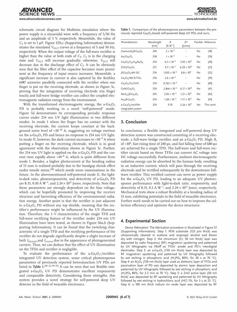
The working principle and performance of the integrated PD system are illustrated in Figure 5. Figure 5a exhibits its equivalent circuit diagram. The first and foremost thing is a contact capacitance Cc formed between the human hand and the receiving electrode when they are in contact with each other. The existence of Cc allows the induced AC signals to pass through the circuit. An oscilloscope is used to manifest the important point, as shown in Figure S2 (Supporting Informa-
tion), where an alternating voltage with a frequency of 50 Hz and an amplitude of ≈1.6 V is clearly observed when putting one finger on the receiving electrode. The frequency is consistent with the main commercial electricity frequency in China, while the amplitude is related with the contact capacitance Cc and the environmental conditions. In addition, a capacitor charging experiment was designed to corroborate the origin of the power energy. The schematic diagram is shown in Figure S3 (Sup-porting Information). The human hand covers the receiving electrode which is connected to the input of the rectifier, and the output end of the rectifier circuit is directly connected to a commercial 1 µF electrolytic capacitor. The experimental pro-cess and the discharging curves for I–V samples are shown in Video S1 and Figure S4 (Supporting Information). The depend-ence of discharge voltage on areas of receiving electrodes, intensity of environmental electromagnetic radiation, and charging time was examined, separately. It should be noted that no discharge voltage is detected for sample V since no charging process was carried out, which indicates that the energy source of the self-powered UV PD system originates from the induc-tive signals generated inside human body.
A constant DC voltage (≈1.25 V) is recorded by the Keithley 2400 ammeter (Figure 5b), which is ascribed to the typical capac-itor filter effect since a test capacitor CT is unavoidably intro-duced in the testing circuit. To support this interpretation, the output characteristics of the full-wave rectifier with and without CT are simulated using Multisim software (National Instru-ment), respectively. Figure S5a (Supporting Information) is the
Figure 5. Working principle and performance of the integrated and self-powered flexible deep UV PD. a) Equivalent circuit diagram. b) DC voltage output of the system when human hand is in contact with the receiving electrode. c) DC current output of the system when human hand is in contact with the receiving electrode. d) The output performance of the system under a periodic 254 nm UV light illumination in two modes. Mode I: photore-sponse of the system with no contact between human finger and receiving electrode; Mode II: photoresponse of the system with a contact between human finger and receiving electrode, when the substrate is flat and bent at r = 15 mm, respectively.
Adv. Mater. Technol. 2021, 6, 2000945
www.advancedsciencenews.com
© 2021 Wiley-VCH GmbH2000945 (6 of 7)
www.advmattechnol.de
schematic circuit diagram for Multisim simulation where the power supply is a sinusoidal wave with a frequency of 5/50 Hz and an amplitude of 5 V, respectively. Meanwhile, the value of CT is set to 1 µF. Figure S5b,c (Supporting Information) demon-strates the simulated VOUT curves at a frequency of 5 and 50 Hz, respectively. When the output voltage of the full-wave rectifier is higher than the value at both ends of CT, CT is in the charging state and VOUT will increase gradually; otherwise, VOUT will decrease due to the discharge effect of CT. It can be obviously seen that the filter effect of the capacitor becomes more promi-nent as the frequency of input source increases. Meanwhile, a significant increase in current is also captured by the Keithley 6487 ammeter parallelly connected with the rectifier when one finger is put on the receiving electrode, as shown in Figure 5c, proving that the integration of receiving electrode (via finger touch) and full-wave bridge rectifier can collect the coupled elec-tromagnetic radiation energy from the environment.
With the transformed electromagnetic energy, the a-Ga2O3 PD is probably working in a novel “self-powered” mode. Figure 5d demonstrates its corresponding periodic response curves under 254 nm UV light illumination in two different modes. In mode I where the finger has no contact with the receiving electrode, the current keeps constant at the back-ground noise level of ≈10−10 A, suggesting no voltage exertion on the a-Ga2O3 PD and hence no response to 254 nm UV light. In mode II, however, the dark current increases to ≈10−9 A when putting a finger on the receiving electrode, which is in good agreement with the observation shown in Figure 5c. Further, the 254 nm UV light is applied on the a-Ga2O3 PD and the cur-rent rises rapidly above ≈10−8 A, which is quite different from mode I. Besides, a higher photocurrent at the bending radius of 15 mm is realized probably due to the bandgap shrink effect under tensile stress,[38] which needs more examinations in the future. In the abovementioned self-powered mode II, the light-to-dark ratio, photoresponsivity, and detectivity of a-Ga2O3 PD are 8.31, 0.10 A W−1, and 2.24 × 10¹¹ Jones, respectively. Note that these parameters are strongly dependent on the bias voltage, which can be hopefully promoted by improving the receiver structure and harvesting efficiency of the environmental radia-tion energy. Another point is that the rectifier is just adjacent to a-Ga2O3 PD without any top shields, meaning that the rec-tifier’s performance might be influenced by the UV illumina-tion. Therefore, the I–V characteristics of the single TFD and full-wave rectifying feature of the rectifier under 254 nm UV illumination have been tested, as shown in Figure S6a,b (Sup-porting Information). It can be found that the switching char-acteristic of a single TFD and the rectifying performance of the rectifier do not degrade significantly despite a slight increase of both Iforward and Ireverse due to the appearance of photogenerated carriers. Thus, we can deduce that the effect of UV illumination on the TFDs and rectifier is negligible.
To evaluate the performance of the a-Ga2O3-/rectifier-integrated UV detection system, some critical photoresponse parameters of previously reported heterojunction UV PDs are listed in Table 1.[18–22,39–43] It can be seen that our flexible inte-grated a-Ga2O3 UV PD demonstrates excellent responsivity and comparable detectivity. Considering these strengths, this system provides a novel strategy for self-powered deep UV detector in the field of wearable electronics.
3. Conclusion
In conclusion, a flexible integrated and self-powered deep UV detection system was constructed consisting of a receiving elec-trode, a full-wave bridge rectifier, and an a-Ga2O3 PD. High Rr of ≈106, fast rising time of 240 µs, and fast falling time of 680 µs are achieved for a single TFD. The half-wave and full-wave rec-tifier circuit based on these TFDs can convert AC voltage into DC voltage successfully. Furthermore, ambient electromagnetic radiation energy can be absorbed by the human body, resulting in an inductive current, which will pass through the receiving electrode and be rectified subsequently by the downstream full-wave rectifier. This rectified current can serve as power supply for the a-Ga2O3 UV PD, leading to an adequate UV photore-sponse performance with light-to-dark ratio, responsivity, and detectivity of 8.31, 0.1 A W−1, and 2.24 × 10¹¹ Jones, respectively. Mechanical tests show a robust flexibility at a bending radius of 15 mm, exhibiting potentials in the field of wearable electronics. Further work needs to be carried out on how to improve the col-lection efficiency and optimize the device structures.
4. Experimental SectionDevice Fabrication: The fabrication procedure is illustrated in Figure S1
(Supporting Information). Step 1: PEN substrate (125 µm thick) was ultrasonically cleaned in acetone and isopropyl alcohol and blown dry with nitrogen. Step 2: the chromium (Cr, 50 nm thick) layer was deposited by radio frequency (RF) magnetron sputtering and patterned by UV lithography via liftoff as TFDs’ anode and PD’s interdigital electrodes. Step 3: an a-Ga2O3 (150 nm thick) layer was deposited by RF magnetron sputtering and patterned by UV lithography followed by wet etching in phosphoric acid (H3PO4 80%, for 30 s at 70 °C). Step 4: an Al2O3 (150 nm thick) layer used as dielectric layer of TFDs and passivation layer of PD was deposited by atomic layer deposition and patterned by UV lithography followed by wet etching in phosphoric acid (H3PO4 80%, for 2.5 min at 70 °C). Step 5: a ZnO active layer (50 nm thick) was deposited by RF sputtering and patterned by UV lithography followed by wet etching in hydrochloric acid (HCl 1%, for 3 s at 25 °C). Step 6: a 100 nm thick indium tin oxide layer was deposited by RF
Table 1. Comparison of the photoresponse parameters between the pre-viously reported Ga2O3-based self-powered deep UV PDs and ours.
Photodetector Wavelength [nm]
R [A W−1]
D* [Jones]
Flexible Reference
Diamond/β-Ga2O3 244 2 × 10⁻⁴ – No [18]
Au/Ga2O3 258 1 × 10⁻⁵ – No [19]
Ga2O3/C81H68N4O8 254 6.5 × 10⁻² 3.95 × 10¹¹ No [20]
ZnO/Ga2O3 251 9.7 × 10⁻³ 6.29 × 10¹² No [21]
β-Ga2O3/4H-SiC 254 1.035 × 10⁻² 8.8 × 10⁹ No [22]
Ga2O3/Nb:SrTiO3 254 2.6 × 10⁻³ – No [39]
Ga2O3/Ga:ZnO 254 0.763 × 10⁻³ – No [40]
GaN/Ga2O3 254 2.844 × 10⁻² 6.17 × 10¹⁰ No [41]
MoS2/β-Ga2O3 245 2.05 × 10⁻³ 1.21 × 10¹¹ No [42]
Au/β-Ga2O3 254 1.28 × 10⁻³ 1.77 × 10¹¹ No [43]
a-Ga2O3/rectifier integrated system
254 0.10 2.24 × 10¹¹ Yes This work
Adv. Mater. Technol. 2021, 6, 2000945
www.advancedsciencenews.com
© 2021 Wiley-VCH GmbH2000945 (7 of 7)
www.advmattechnol.de
magnetron sputtering and also patterned by UV lithography together with a liftoff process to define the top contacts of TFDs and form the electrical connection between full-wave rectifier circuit and the PD as well as the receiving electrode.
Device Characterization: The electrical properties of the TFDs were analyzed using a Keithley 4200 semiconductor characterization system. The half-wave rectification characteristics of a single TFD and full-wave rectification characteristics of a rectifier were tested by an oscilloscope (Tektronix TDS1000B-SC) via P2220 passive voltage probes. The electrical characteristic measurements of a-Ga2O3 UV PD were carried out using a Keithley 6487 picoammeter and a handheld 254 nm UV lamp (ZF-5) as the light source. Photoresponsivity measurements were performed using a Xe lamp monochromatized by the Omni-λ 180i grating spectrometer as the light source and Keithley 6487 picoammeter as the photocurrent monitor.
Supporting InformationSupporting Information is available from the Wiley Online Library or from the author.
AcknowledgementsThis work was supported by the National Natural Science Foundation of China (Grant Nos. 11675280, 11674405, 61874139, 11875088, and 61904201).
Conflict of InterestThe authors declare no conflict of interest.
Keywordsamorphous gallium oxide, environmental electromagnetic radiation energy, flexible self-powered system, UV photodetectors
Received: September 22, 2020Revised: November 14, 2020
Published online: February 8, 2021
[1] X. Du, Z. Mei, Z. Liu, Y. Guo, T. Zhang, Y. Hou, Z. Zhang, Q. Xue, A. Y. Kuznetsov, Adv. Mater. 2009, 21, 4625.
[2] Y. N. Hou, Z. X. Mei, H. L. Liang, D. Q. Ye, C. Z. Gu, X. L. Du, Appl. Phys. Lett. 2013, 102, 153510.
[3] Y. N. Hou, Z. X. Mei, H. L. Liang, C. Z. Gu, X. L. Du, Appl. Phys. Lett. 2014, 105, 133510.
[4] E. Cicek, R. McClintock, C. Y. Cho, B. Rahnema, M. Razeghi, Appl. Phys. Lett. 2013, 103, 191108.
[5] D. Walker, V. Kumar, K. Mi, P. Sandvik, P. Kung, X. H. Zhang, M. Razeghi, Appl. Phys. Lett. 2000, 76, 403.
[6] F. Foulon, P. Bergonzo, C. Borel, R. D. Marshall, C. Jany, L. Besombes, A. Brambilla, D. Riedel, L. Museur, M. C. Castex, A. Gicquel, J. Appl. Phys. 1998, 84, 5331.
[7] S. Cui, Z. Mei, Y. Zhang, H. Liang, X. Du, Adv. Opt. Mater. 2017, 5, 1700454.
[8] Z. Han, H. Liang, W. Huo, X. Zhu, X. Du, Z. Mei, Adv. Opt. Mater. 2020, 8, 1901833.
[9] W.-Y. Kong, G.-A. Wu, K.-Y. Wang, T.-F. Zhang, Y.-F. Zou, D.-D. Wang, L.-B. Luo, Adv. Mater. 2016, 28, 10725.
[10] Y. Teng, L. X. Song, A. Ponchel, Z. K. Yang, J. Xia, Adv. Mater. 2014, 26, 6238.
[11] Y. Li, T. Tokizono, M. Liao, M. Zhong, Y. Koide, I. Yamada, J.-J. Delaunay, Adv. Funct. Mater. 2010, 20, 3972.
[12] R. Zou, Z. Zhang, Q. Liu, J. Hu, L. Sang, M. Liao, W. Zhang, Small 2014, 10, 1848.
[13] X. Chen, F. Ren, S. Gu, J. Ye, Photonics Res. 2019, 7, 381.[14] Y. Kokubun, K. Miura, F. Endo, S. Nakagomi, Appl. Phys. Lett. 2007,
90, 031912.[15] B. Zhao, F. Wang, H. Chen, Y. Wang, M. Jiang, X. Fang, D. Zhao,
Nano Lett. 2015, 15, 3988.[16] H. Liang, S. Cui, R. Su, P. Guan, Y. He, L. Yang, L. Chen, Y. Zhang,
Z. Mei, X. Du, ACS Photonics 2019, 6, 351.[17] Y. Sui, H. Liang, Q. Chen, W. Huo, X. Du, Z. Mei, ACS Appl. Mater.
Interfaces 2020, 12, 8929.[18] Y.-C. Chen, Y.-J. Lu, C.-N. Lin, Y.-Z. Tian, C.-J. Gao, L. Dong,
C.-X. Shan, J. Mater. Chem. C 2018, 6, 5727.[19] X. Chen, K. Liu, Z. Zhang, C. Wang, B. Li, H. Zhao, D. Zhao,
D. Shen, ACS Appl. Mater. Interfaces 2016, 8, 4185.[20] Z. Yan, S. Li, Z. Liu, Y. Zhi, J. Dai, X. Sun, S. Sun, D. Guo, X. Wang,
P. Li, Z. Wu, L. Li, W. Tang, J. Mater. Chem. C 2020, 8, 4502.[21] B. Zhao, F. Wang, H. Chen, L. Zheng, L. Su, D. Zhao, X. Fang, Adv.
Funct. Mater. 2017, 27, 1700264.[22] J. Yu, L. Dong, B. Peng, L. Yuan, Y. Huang, L. Zhang, Y. Zhang,
R. Jia, J. Alloys Compd. 2020, 821, 153532.[23] J. Xu, W. Zheng, F. Huang, J. Mater. Chem. C 2019, 7, 8753.[24] M. M. Muhammed, M. Peres, Y. Yamashita, Y. Morishima, S. Sato,
N. Franco, K. Lorenz, A. Kuramata, I. S. Roqan, Appl. Phys. Lett. 2014, 105, 042112.
[25] Y. Li, W. Zhong, W. Zheng, F. Huang, IEEE Electron Device Lett. 2020, 41, 1316.
[26] D. Poljak, C. Y. Tham, N. Kovac, Eng. Anal. Boundary Elem. 2003, 27, 999.
[27] M. Cavagnaro, E. Pittella, S. Pisa, Int. J. Antennas Propag. 2013, 2013, 1.
[28] H. Wang, IEEE Open J. Antennas Propag. 2020, 1, 113.[29] Y. Zhang, Z. Mei, S. Cui, H. Liang, Y. Liu, X. Du, Adv. Electron.
Mater. 2016, 2, 1500486.[30] Y. Zhang, Z. Mei, T. Wang, W. Huo, S. Cui, H. Liang, X. Du, Nano
Energy 2017, 40, 289.[31] Y. Zhang, Z. Mei, W. Huo, T. Wang, H. Liang, X. Du, J. Phys. D: Appl.
Phys. 2018, 51, 175102.[32] Y. Zhang, Z. Mei, W. Huo, T. Wang, H. Liang, X. Du, Microelectron.
Eng. 2018, 199, 92.[33] Y. Kang, H. Song, H.-H. Nahm, S. H. Jeon, Y. Cho, S. Han, APL
Mater. 2014, 2, 032108.[34] E. A. Davis, N. F. Mott, Philos. Mag. 1970, 22, 0903.[35] G. Schmitz, P. Gassmann, R. Franchy, J. Appl. Phys. 1998, 83,
2533.[36] Z. Hajnal, J. Miró, G. Kiss, F. Réti, P. Deák, R. C. Herndon,
J. M. Kuperberg, J. Appl. Phys. 1999, 86, 3792.[37] L. Huang, Q. Feng, G. Han, F. Li, X. Li, L. Fang, X. Xing, J. Zhang,
Y. Hao, IEEE Photonics J. 2017, 9, 1.[38] W. S. Yun, S. W. Han, S. C. Hong, I. G. Kim, J. D. Lee, Phys. Rev. B
2012, 85, 033305.[39] D. Guo, H. Liu, P. Li, Z. Wu, S. Wang, C. Cui, C. Li, W. Tang, ACS
Appl. Mater. Interfaces 2017, 9, 1619.[40] Z. Wu, L. Jiao, X. Wang, D. Guo, W. Li, L. Li, F. Huang, W. Tang, J.
Mater. Chem. C 2017, 5, 8688.[41] P. Li, H. Shi, K. Chen, D. Guo, W. Cui, Y. Zhi, S. Wang, Z. Wu,
Z. Chen, W. Tang, J. Mater. Chem. C 2017, 5, 10562.[42] R. Zhuo, D. Wu, Y. Wang, E. Wu, C. Jia, Z. Shi, T. Xu, Y. Tian, X. Li, J.
Mater. Chem. C 2018, 6, 10982.[43] L. Dong, J. Yu, R. Jia, J. Hu, Y. Zhang, J. Sun, Opt. Mater. Express
2019, 9, 1191.
Adv. Mater. Technol. 2021, 6, 2000945