![Hybrid Monte-Carlo simulations of electronic properties of graphene [ ArXiv:1206.0619]](https://static.fdocument.org/doc/165x107/56816623550346895dd97a94/hybrid-monte-carlo-simulations-of-electronic-properties-of-graphene-arxiv12060619-56cd59ad91d40.jpg)
Hybrid Monte-Carlo simulations of electronic properties of graphene [ ArXiv:1206.0619]
Published: October 27, 2011
r 2011 American Chemical Society 2897 dx.doi.org/10.1021/jz201273r | J. Phys. Chem. Lett. 2011, 2, 2897–2905
PERSPECTIVE
pubs.acs.org/JPCL
Tailoring Electronic Properties of Graphene by π�π Stacking withAromatic MoleculesZengxing Zhang,† Helin Huang,‡ Xiaomei Yang,‡ and Ling Zang*,‡
†Shanghai Key Laboratory of Special Artificial Microstructure Materials and Technology & Department of Physics, Tongji University,Shanghai 200092, China‡Department of Materials Science and Engineering, University of Utah, Salt Lake City, Utah 84108, United States
Graphene, a single atomic layer of SP2-hybridized carbonatoms with honeycomb structure, has been attracting great
deal of research interest due to its variable applications. Severalperspective articles have already highlighted the recent researchprogress of graphene, particularly from the point of view ofphysical chemistry.1�6 Distinct from these perspectives, weherein specifically focus on how to tailor the electronic propertiesof graphene through noncovalent π�π stacking with aromaticmolecules, which ismainly determined by theπ�π interaction inconjunction with electron donor�acceptor (charge transfer)interaction. Different types of molecules (functioning as eitherelectron donor or acceptor) as reported in recent literature arepresented regarding surface patterning, bandgap engineering,surface doping, as well as applications in nanodevices, particularlyfield-effect transistors (FETs).
Graphene possesses unique properties of high carriermobility, long phase coherence length, high thermal con-ductivity, and strong mechanical behavior, which combinedmake it a promising material for future carbon-based nano-electronics.7�12 However, the valence and conduction bands ofintrinsic graphene intersect at the Dirac point in the corners of ahexagonal Brillouin zone, making graphene a semimetal or so-called zero bandgap semiconductor. This hinders the develop-ment of graphene for application in nanoelectronics. In order toapproach high-performance electronic devices, it is essential togenerate bandgap in graphene to enable its semiconductingbehavior and precisely control the charge carrier type (p-type vsn-type) and density.
So far, several approaches have been attempted to tailor theelectronic properties of graphene. Atomic doping (e.g., by boronor nitrogen) as employed in traditional semiconductors hasproven to be able to open the bandgap and make p-type orn-type graphene.13�15 However, the doping is usually difficultto control and often introduces defects and thus destroys theband structure. Another way is to modify graphene by covalent
modification, where the absorbed molecules form chemicalbonds to the graphene surface.14,16,17 This type of chemicalmodification can usually generate stable structures, and repre-sents one of the most promising methods for increasing thesolution processability for printable graphene electronics. However,the covalent bonding changes the graphene’s carbon hybridizationfrom SP2 to SP3, often leading to unwanted alteration or evendestruction of the basic electronic properties of graphene.
Alternatively, the electronic properties of graphene can betuned by noncovalent modification. Under such conditions, theinteraction between absorbates and graphene surface are dis-persive, which can preserve the desired electronic properties ofgraphene by minimizing the damage to the carbon lattice. Due tothe large specific surface area of graphene sheet, the electroniceffect caused by this kind of surface modification could besignificant, providing a simple, but effective way to tailor thebandgap structure of graphene. Moreover, in the past decades,aromatic molecules have often been employed to modifythe electronic properties of carbon nanotubes (CNTs).18,19
In order to approach high-perfor-mance electronic devices, it is es-sential to generate bandgap ingraphene to enable its semicon-
ducting behavior.
Received: September 19, 2011Accepted: October 27, 2011
ABSTRACT: Intrinsic graphene is a semimetal or zero bandgap semiconductor, which hinders itsapplications for nanoelectronics. To develop high-performance nanodevices with graphene, it isnecessary to open the bandgap and precisely control the charge carrier type and density. In thisperspective, we focus on tailoring the electronic properties of graphene by noncovalent stacking witharomatic molecules through π�π interaction. Different types of molecules (functioning as either anelectron donor or acceptor when stacked with graphene) as reported in recent literature are presentedregarding surface patterning, bandgap engineering, surface doping, aswell as applications in nanodevices,particularly the field-effect transistors (FETs). On the basis of the current progress along this researchline, future issues and challenges are also briefly discussed.
2898 dx.doi.org/10.1021/jz201273r |J. Phys. Chem. Lett. 2011, 2, 2897–2905
The Journal of Physical Chemistry Letters PERSPECTIVE
The molecules interact with the sidewall of CNTs by means ofthe so-named π�π stacking, a kind of van der Waals forcerelating to their π-electron backbone system, to form a stablehybrid structure and improve their electronic properties. Theπ�π stacking modification has been demonstrated to do muchto preserve the desired properties. Graphene surface has a similargraphitic structure to the sidewall of CNTs; however, graphenepossesses a planar π-surface that is more conducive to cofacialπ�π stacking. It is thus expected that the noncovalent π�πstacking will open a promising way to precisely tailor theelectronic properties of graphene so as to be suited for futureapplication in nanoelectronics.
Stacking Aromatic Molecules on a Graphene Surface. Aromaticmolecules, such as tetrafluorotetracyanoquinodimethanes (F4-TCNQ), perylene-3,4,9,10-tetracarboxylic-3,4,9,10-diimide (PTCDI),and its precursor perylene-3,4,9,10-tetracarboxylic-3,4,9,10-di-anhydride (PTCDA), have been widely used in organic semi-conductors, as these molecules are proven effective for inter-molecular π�π stacking through self-assembly processing.20,21
Recently, these aromatic molecules have been investigated forπ�π stacking assembly on a graphene surface, where significantchange of the electronic properties of graphene was observed,accompanied by efficient interfacial charge transfer.22�24 Thesearomatic molecules can be assembled on a graphene surface bythe physical vapor deposition (PVD) method in an ultrahighvacuum (UHV) chamber.25,26 By this method, the surface cover-age and layers of molecules can be controlled by the depositingtime, the molecular pressure, and the state of the graphene surfaceincluding temperature, undulation, defects, and so on. Thearomatic molecules can also be transferred on graphene surfaceby drop-casting the solutions or immersing graphene samples inthe solutions.With either ofmethods, the surface coverage can beadjusted by the concentration, the contacting time, and the rinsingafterward. The strong π�π stacking between the graphenesurface and the aromatic molecules usually makes the surfacestacking quite stable against rinsing or other solution processing.
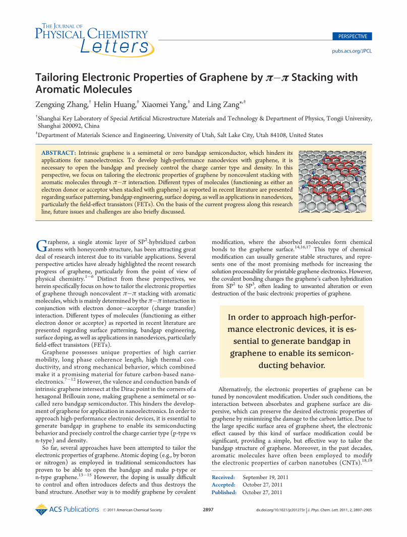
By using scanning tunneling microscopy (STM), severalgroups investigated self-assembled PTCDA molecules on agraphene surface.23,25,26 PTCDA is a planar molecule based ona perylene backbone with a conjugated shape-persistent π-electron system (as shown in Figure 1a), which is highly suitedfor stacking onto a graphene surface. Besides tailoring theelectronic properties, PTCDA derivatives were found to playan important role in the deposition of uniform ultrathin Al2O3
film that could act as high-k dielectrics for future nano-electronics.27 By low-temperature STM, Lauffer et al. found thatPTCDA molecules can self-assemble on a bilayer graphenesurface with a nonplanar brick-wall structure at a high density.23
Although this specific phase may not be stable under ambient
conditions, as they could only exit at 4.7 K, a stable, well-ordered,uniform monolayer of PTCDA molecules with herringbonestructure was self-assembled on a graphene surface at 77 K oreven room temperature.25,26
Figure 1b,c show room-temperature STM images of mono-layer PTCDA molecules self-assembled on a graphene surface.The PTCDA molecules are well-ordered with large domainsover hundreds of nanometers. Figure 1c is a molecular-resolu-tion STM image. A herringbone structure of PTCDAmoleculeswas clearly observed, where PTCDA molecules lie flatly on thegraphene surface with their π-planes parallel to the surface,exhibiting clear evidence that the PTCDA molecules areassembled on the graphene surface through π�π interaction.Furthermore, the herringbone monolayer of PTCDA mole-cules on graphene is stable even under laboratory ambientconditions.25
Figure 1. (a) Molecular structure of PTCDA. (b) STM image of thePTCDA monolayer assembled on a graphene surface. (c) Molecular-resolution STM image of the PTCDA monolayer. (d) Schematicherringbone unit cell of the PTCDA monolayer. (Adapted from ref 25with permission. Copyright 2009, Macmillan Publishers Ltd.)
Graphene surface has a similar gra-phitic structure to the sidewall ofCNTs; however, graphene possessesa planar π-surface that is more
conducive to cofacial π�π stacking.
2899 dx.doi.org/10.1021/jz201273r |J. Phys. Chem. Lett. 2011, 2, 2897–2905
The Journal of Physical Chemistry Letters PERSPECTIVE
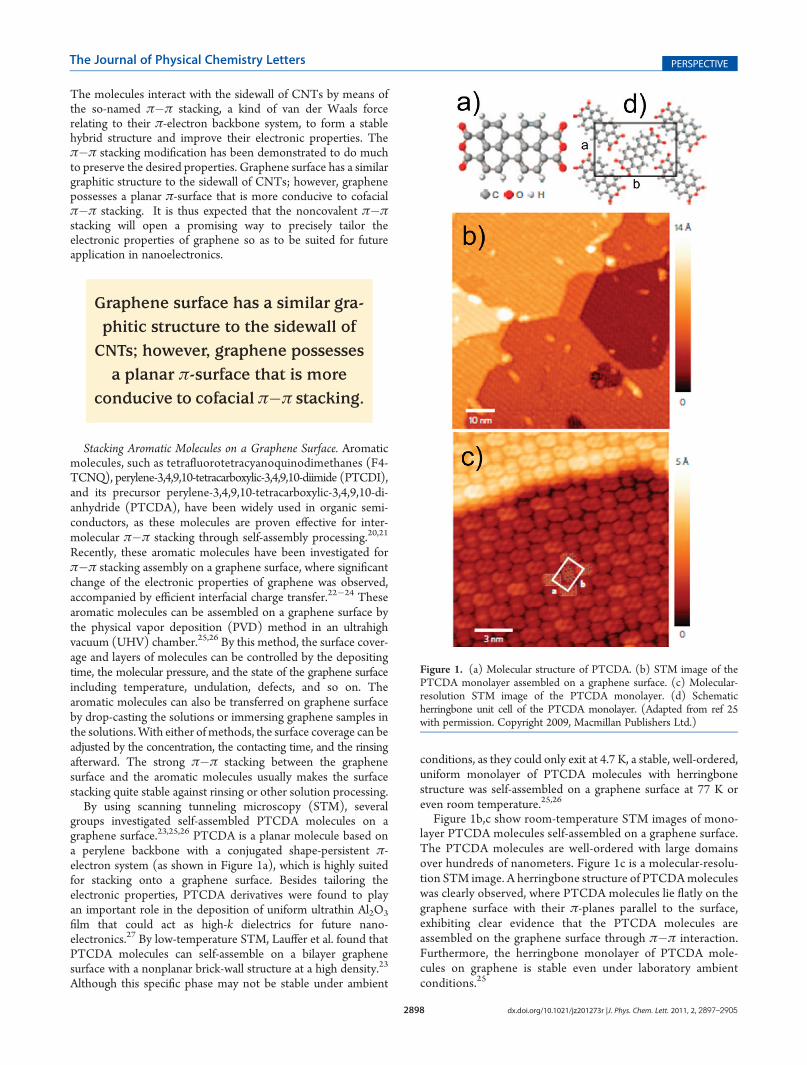
The assembly of PTCDA molecules as stacked on a graphenesurface was also studied by density functional theory (DFT)-based ab initio calculation.28 The results exhibit that a singlePTCDA molecule is thermodynamically stable with the geome-try configuration as shown in Figure 2a. In such a situation, theaverage distance between PTCDA molecules and the graphenesurface is around 3.11 Å, and the absorption energy is 1.20 eV,which is the largest among other stacking configurations.Figure 2b shows an optimized structure of PTCDA moleculeswhen forming a complete monolayer on a graphene surface. Herethe PTCDA molecules form a herringbone structure, which isconsistent with the experimental results obtained by STMimaging (Figure 1).25,26 These molecules are stabilized by two typesof interactions, in-plane intermolecular interaction between thePTCDA molecules, and the PTCDA�graphene π�π interaction.
Bandgap Engineering. Some of the aromatic molecules such asPTCDI, 1,10-azobis(cyanocyclohexane) (ACN), F4-TCNQ and1,3,6,8-pyrenetetrasulfonic acid (TPA) can induce bandgap ingraphene when they stack onto a graphene surface by π�πinteraction.29�32 This noncovalent modification does not lead to
damage of the desired electronic properties of graphene, thusopening a simple way to engineer the bandgap of graphene.
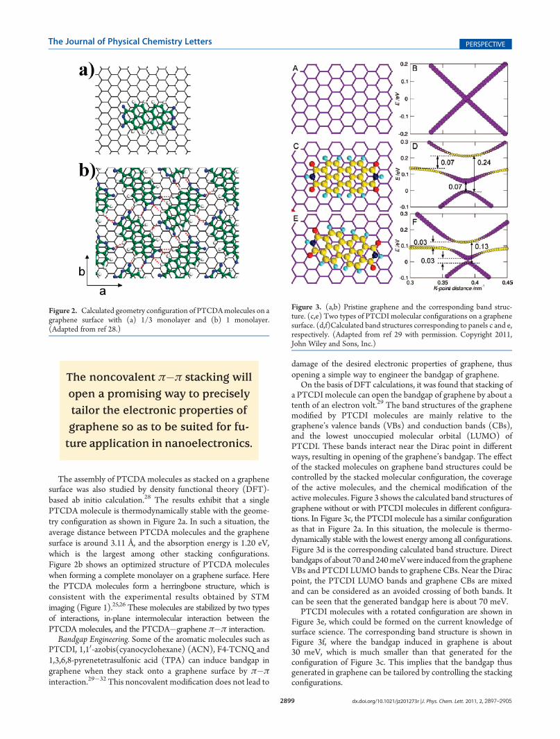
On the basis of DFT calculations, it was found that stacking ofa PTCDI molecule can open the bandgap of graphene by about atenth of an electron volt.29 The band structures of the graphenemodified by PTCDI molecules are mainly relative to thegraphene’s valence bands (VBs) and conduction bands (CBs),and the lowest unoccupied molecular orbital (LUMO) ofPTCDI. These bands interact near the Dirac point in differentways, resulting in opening of the graphene’s bandgap. The effectof the stacked molecules on graphene band structures could becontrolled by the stacked molecular configuration, the coverageof the active molecules, and the chemical modification of theactivemolecules. Figure 3 shows the calculated band structures ofgraphene without or with PTCDI molecules in different configura-tions. In Figure 3c, the PTCDI molecule has a similar configurationas that in Figure 2a. In this situation, the molecule is thermo-dynamically stable with the lowest energy among all configurations.Figure 3d is the corresponding calculated band structure. Directbandgaps of about 70 and 240meVwere induced from the grapheneVBs and PTCDI LUMO bands to graphene CBs. Near the Diracpoint, the PTCDI LUMO bands and graphene CBs are mixedand can be considered as an avoided crossing of both bands. Itcan be seen that the generated bandgap here is about 70 meV.
PTCDI molecules with a rotated configuration are shown inFigure 3e, which could be formed on the current knowledge ofsurface science. The corresponding band structure is shown inFigure 3f, where the bandgap induced in graphene is about30 meV, which is much smaller than that generated for theconfiguration of Figure 3c. This implies that the bandgap thusgenerated in graphene can be tailored by controlling the stackingconfigurations.
Figure 3. (a,b) Pristine graphene and the corresponding band struc-ture. (c,e) Two types of PTCDI molecular configurations on a graphenesurface. (d,f)Calculated band structures corresponding to panels c and e,respectively. (Adapted from ref 29 with permission. Copyright 2011,John Wiley and Sons, Inc.)
Figure 2. Calculated geometry configuration of PTCDAmolecules on agraphene surface with (a) 1/3 monolayer and (b) 1 monolayer.(Adapted from ref 28.)
The noncovalent π�π stacking willopen a promising way to preciselytailor the electronic properties ofgraphene so as to be suited for fu-ture application in nanoelectronics.
2900 dx.doi.org/10.1021/jz201273r |J. Phys. Chem. Lett. 2011, 2, 2897–2905
The Journal of Physical Chemistry Letters PERSPECTIVE
The induced bandgap of graphene can also be tuned by thecoverage of PTCDI molecules. The above-mentioned PTCDImolecular coverage on graphene surface is about 0.388 mole-cules/nm2. Herringbone and brick-wall configuration are twotypical structures observed for PTCDI molecules when stackedon a graphene surface at higher coverage of 0.677 and 0.595molecules/nm2, respectively. The herringbone structure leads to abandgap of about 80 meV near the Dirac point, and the brick-wallstructure leads to a bandgap of about 90 meV.29 These calculatedresults confirm that the bandgap generated within graphene issomehow dependent on the surface coverage of active molecules.
Since the PTCDI LUMO band plays an important role intuning the bandgap of graphene, one may attempt to gain thedesired LUMO level by chemical modification of PTCDImolecules as shown in Table 1. The bay area of PTCDI isfeasible for substitution with variable electron donor or acceptormoieties so as to shift the LUMO up or down. For the fourmolecules shown in Table 1, the LUMO can be tuned as large as0.6 eV, while the bandgap remains almost unchanged around2.5 eV. In the past decade, various PTCDI derivatives have beendesigned and synthesized in our lab, and the self π�π stackinginteractions of these molecules have been extensivelystudied.20,33�40 The wide range of LUMO levels as attained forthese modified PTCDI molecules will likely enable furtheradjustment of the bandgap of graphene. Moreover, the enhancedelectron accepting capability of the cyano-substituted PTCDI isconducive to the lc p-type doping of graphene.
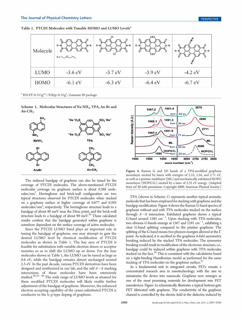
TPA (shown in Scheme 1) represents another typical aromaticmolecule that has been employed for stackingwith graphene and thebandgapmodification. Figure 4 shows the RamanG-band spectra ofgraphene without and with TPA molecules stacked on the surfacethrough π�π interaction. Exfoliated graphene shows a typicalG-band around 1585 cm�1. Upon stacking with TPA molecules,two obvious G-bands emerge at 1567 and 1591 cm�1, exhibiting aclear G-band splitting compared to the pristine graphene. Thesplitting of theG-bandmeans two phonon energies allowed at theΓpoint. As indicated, it is ascribed to the graphene 6-fold asymmetrybreaking induced by the stacked TPA molecules. The symmetrybreaking would result inmodification of the electronic structure, i.e.,bandgap could be induced within graphene with TPA moleculesstacked on the face.30 This is consistent with the calculations basedon a tight-binding Hamiltonian model as performed for the samestacking of TPA molecules on the graphene surface.31
As a fundamental unit in integrated circuits, FETs remain aconcentrated research area in nanotechnology, with the aim tominiaturize the device into nanoscale. Graphene now emerges asone of the most promising materials for development into FETnanodevices. Figure 5a schematically illustrates a typical bottom-gateFET fabricated with graphene. The conductivity of the graphenechannel is controlled by the electric field in the dielectric induced by
Table 1. PTCDI Molecules with Tunable HOMO and LUMO Levelsa
aB3LYP/6-311g**//b3lyp/6-31g*, Gaussian 09 package.
Scheme 1. Molecular Structures of Na-NH2, TPA, An-Br andAn-CH3
Figure 4. Raman G and 2D bands of a TPA-modified graphenemonolayer excited by lasers with energies of 2.33, 2.54, and 2.71 eV,as well as a pristine multilayer (ML) and mechanically exfoliated HOPGmonolayer (HOPG1L) excited by a laser of 2.33 eV energy. (Adaptedfrom ref 30 with permission. Copyright 2009, American Physical Society.)
2901 dx.doi.org/10.1021/jz201273r |J. Phys. Chem. Lett. 2011, 2, 2897–2905
The Journal of Physical Chemistry Letters PERSPECTIVE
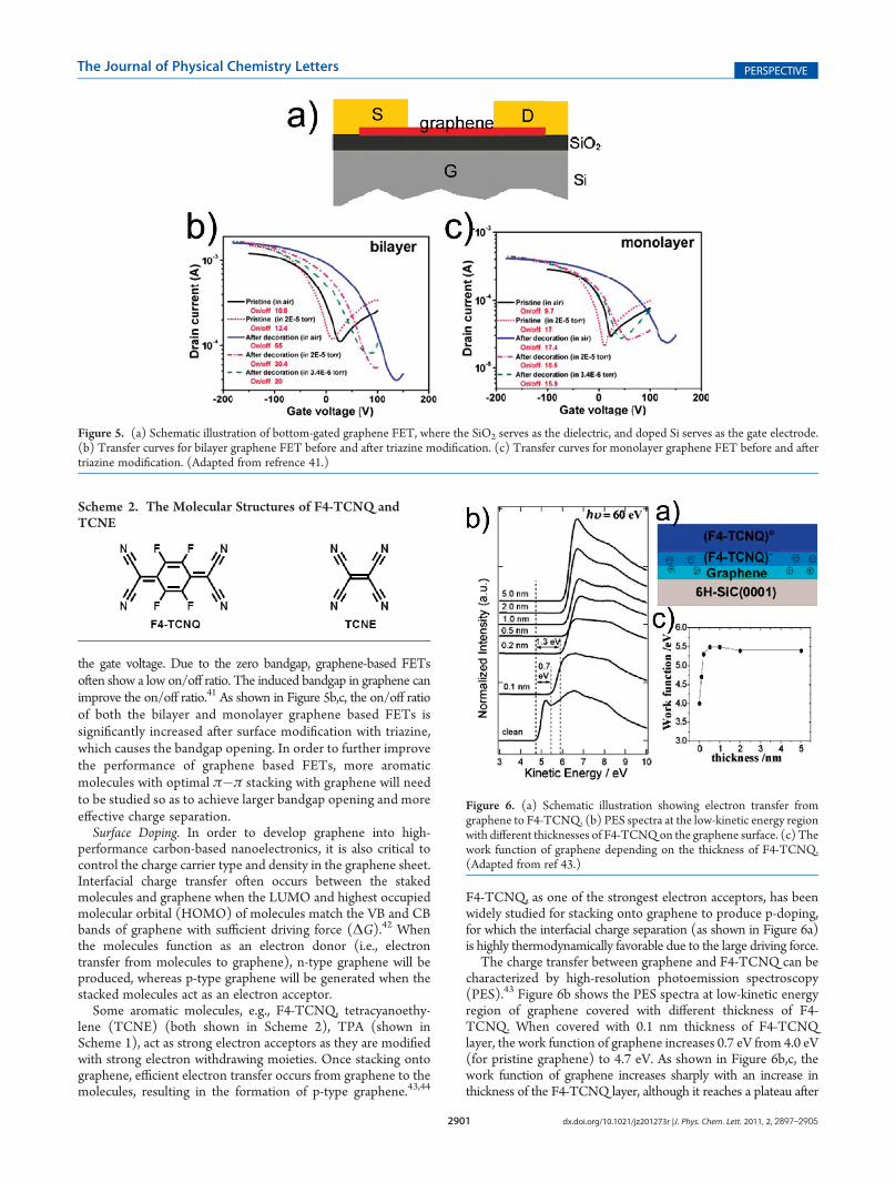
the gate voltage. Due to the zero bandgap, graphene-based FETsoften show a low on/off ratio. The induced bandgap in graphene canimprove the on/off ratio.41 As shown in Figure 5b,c, the on/off ratioof both the bilayer and monolayer graphene based FETs issignificantly increased after surface modification with triazine,which causes the bandgap opening. In order to further improvethe performance of graphene based FETs, more aromaticmolecules with optimal π�π stacking with graphene will needto be studied so as to achieve larger bandgap opening and moreeffective charge separation.
Surface Doping. In order to develop graphene into high-performance carbon-based nanoelectronics, it is also critical tocontrol the charge carrier type and density in the graphene sheet.Interfacial charge transfer often occurs between the stakedmolecules and graphene when the LUMO and highest occupiedmolecular orbital (HOMO) of molecules match the VB and CBbands of graphene with sufficient driving force (ΔG).42 Whenthe molecules function as an electron donor (i.e., electrontransfer from molecules to graphene), n-type graphene will beproduced, whereas p-type graphene will be generated when thestacked molecules act as an electron acceptor.
Some aromatic molecules, e.g., F4-TCNQ, tetracyanoethy-lene (TCNE) (both shown in Scheme 2), TPA (shown inScheme 1), act as strong electron acceptors as they are modifiedwith strong electron withdrawing moieties. Once stacking ontographene, efficient electron transfer occurs from graphene to themolecules, resulting in the formation of p-type graphene.43,44
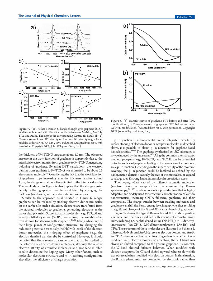
F4-TCNQ, as one of the strongest electron acceptors, has beenwidely studied for stacking onto graphene to produce p-doping,for which the interfacial charge separation (as shown in Figure 6a)is highly thermodynamically favorable due to the large driving force.
The charge transfer between graphene and F4-TCNQ can becharacterized by high-resolution photoemission spectroscopy(PES).43 Figure 6b shows the PES spectra at low-kinetic energyregion of graphene covered with different thickness of F4-TCNQ. When covered with 0.1 nm thickness of F4-TCNQlayer, the work function of graphene increases 0.7 eV from 4.0 eV(for pristine graphene) to 4.7 eV. As shown in Figure 6b,c, thework function of graphene increases sharply with an increase inthickness of the F4-TCNQ layer, although it reaches a plateau after
Figure 5. (a) Schematic illustration of bottom-gated graphene FET, where the SiO2 serves as the dielectric, and doped Si serves as the gate electrode.(b) Transfer curves for bilayer graphene FET before and after triazine modification. (c) Transfer curves for monolayer graphene FET before and aftertriazine modification. (Adapted from refrence 41.)
Scheme 2. The Molecular Structures of F4-TCNQ andTCNE
Figure 6. (a) Schematic illustration showing electron transfer fromgraphene to F4-TCNQ. (b) PES spectra at the low-kinetic energy regionwith different thicknesses of F4-TCNQon the graphene surface. (c) Thework function of graphene depending on the thickness of F4-TCNQ.(Adapted from ref 43.)
2902 dx.doi.org/10.1021/jz201273r |J. Phys. Chem. Lett. 2011, 2, 2897–2905
The Journal of Physical Chemistry Letters PERSPECTIVE
the thickness of F4-TCNQ surpasses about 1.0 nm. The observedincrease in the work function of graphene is apparently due to theinterfacial electron transfer from graphene to F4-TCNQ, generatingp-doping of graphene. By using DFT calculations, the electrontransfer from graphene to F4-TCNQwas estimated to be about 0.3electron permolecule.44 Considering the fact that the work functionof graphene stops increasing after the thickness reaches around1 nm, the charge separation is likely limited to the interface domain.The result shown in Figure 6 also implies that the charge carrierdensity within graphene may be modulated by changing thethickness (or density) of the surface stacked molecules.
Similar to the approach as illustrated in Figure 6, n-typegraphene can be realized by stacking electron donor moleculeson the surface. In such a situation, electrons are transferred fromthe stacked molecules to graphene, generating electrons as themajor charge carrier. Some aromatic molecules, e.g., PTCDI andvanadyl-phthalocyamine (VOPc) are among the suitable elec-tron donors for stacking with graphene,23,42 taking advantage oftheir large planar π-configuration structure. By changing thereduction potential (essentially the HOMO level) of the electrondonor molecules, the n-doping effect of graphene (e.g., theelectron density) can thereby be controlled. However, it shouldbe noted that there seems no simple rule that can be applied tothe selection of effective doping molecules, although the relativeelectron affinity of aromatic molecules and graphene is oftenused to determine the doping type. Many other factors, such asmolecular electronic structure and π�π stacking configuration,also affect the efficiency of charge separation.
p�n junction is a fundamental unit in integrated circuits. Bysurface stacking of electron donor or acceptor molecules as describedabove, it is possible to obtain p�n junctions for graphene-basednanoelectronics.45,46 The graphene synthesized on SiC substrates isn-type induced by the substrates.47 Using the common thermal vapormethod, p-dopants, e.g., F4-TCNQ and TCNE, can be assembledonto the surface of graphene, leading to the formation of a molecularscale p�n junction.Depending on the surface density of themoleculecoverage, the p�n junction could be localized as defined by thenanojunction domain (basically the size of the molecule), or expandto a large area if strong lateral intermolecular association exists.
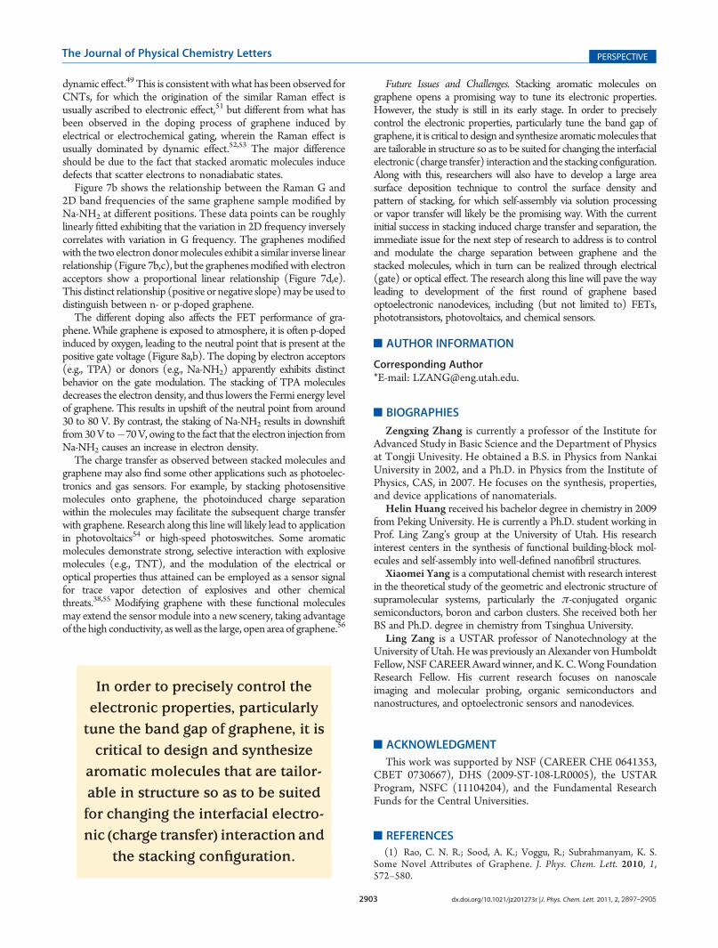
The doping effect caused by different aromatic molecules(electron donor vs acceptor) can be examined by Ramanspectroscopy,48�50 which represents a powerful tool that is highlyadaptable and widely used for structural characterization of carbonnanostructures, including CNTs, fullerene, graphene, and theircomposites. The charge transfer between stacking molecules andgraphene can shift the Fermi energy level in graphene, thus resultingin significant change of the G and 2D Raman bands of graphene.
Figure 7a shows the typical Raman G and 2D bands of pristinegraphene and the ones modified with a series of aromatic mole-cules, including 1,5-naphthalenediamine (Na-NH2), 9,10-dimethy-lanthracene (An-CH3), 9,10-dibromoanthracene (An-Br), andTPA. The structures of these molecules are illustrated in Scheme 1.Therein, Na-NH2 andAn-CH3 serve as electron donors, and An-Brand TPA serve as electron acceptors. Regardless of whether it wasmodified with electron donors or acceptors, the 2D band wasalways up-shifted compared to the pristine graphene. By contrast,the G band showed different behavior. When modified withelectron acceptors, the G band shifted upward, whereas downshiftwas observedwhenmodifiedwith electron donors. In this situation,the Raman phenomena are dominated by electronic rather than
Figure 7. (a) The left is Raman G bands of single layer graphene (SLG)modifiedwithout andwith different aromaticmolecules ofNa-NH2,An-CH3,TPA, and An-Br. The right is the corresponding Raman 2D bands. (b�e)Curves showingRaman2D intensity as a functionofG intensity for graphenesmodifiedwithNa-NH2,An-CH3,TPA, andAn-Br. (Adapted fromref 49withpermission. Copyright 2009, John Wiley and Sons, Inc.)
Figure 8. (a) Transfer curves of graphene FET before and after TPAmodification. (b) Transfer curves of graphene FET before and afterNa-NH2modification. (Adapted from ref 49 with permission. Copyright2009, John Wiley and Sons, Inc.)
2903 dx.doi.org/10.1021/jz201273r |J. Phys. Chem. Lett. 2011, 2, 2897–2905
The Journal of Physical Chemistry Letters PERSPECTIVE
dynamic effect.49 This is consistentwithwhat has been observed forCNTs, for which the origination of the similar Raman effect isusually ascribed to electronic effect,51 but different from what hasbeen observed in the doping process of graphene induced byelectrical or electrochemical gating, wherein the Raman effect isusually dominated by dynamic effect.52,53 The major differenceshould be due to the fact that stacked aromatic molecules inducedefects that scatter electrons to nonadiabatic states.
Figure 7b shows the relationship between the Raman G and2D band frequencies of the same graphene sample modified byNa-NH2 at different positions. These data points can be roughlylinearly fitted exhibiting that the variation in 2D frequency inverselycorrelates with variation in G frequency. The graphenes modifiedwith the two electron donormolecules exhibit a similar inverse linearrelationship (Figure 7b,c), but the graphenesmodifiedwith electronacceptors show a proportional linear relationship (Figure 7d,e).This distinct relationship (positive or negative slope)may be used todistinguish between n- or p-doped graphene.
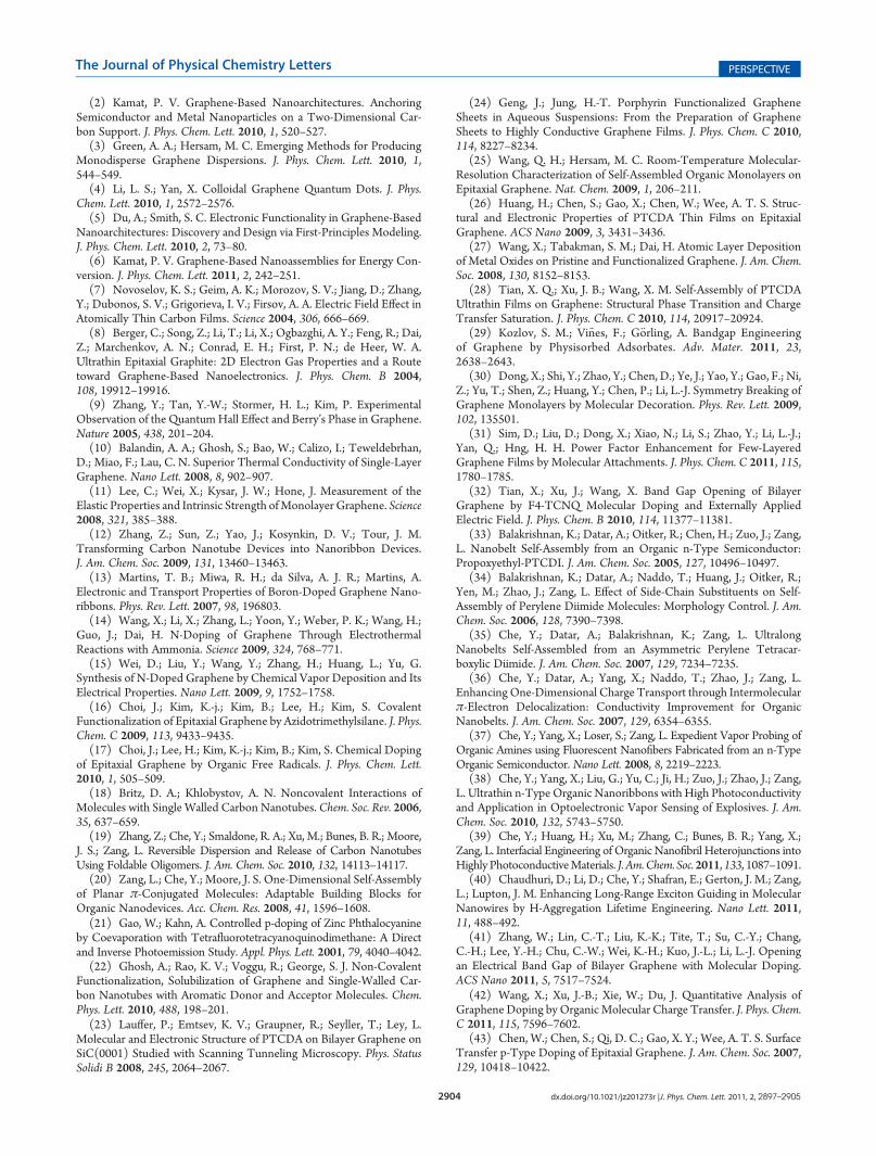
The different doping also affects the FET performance of gra-phene. While graphene is exposed to atmosphere, it is often p-dopedinduced by oxygen, leading to the neutral point that is present at thepositive gate voltage (Figure 8a,b). The doping by electron acceptors(e.g., TPA) or donors (e.g., Na-NH2) apparently exhibits distinctbehavior on the gate modulation. The stacking of TPA moleculesdecreases the electron density, and thus lowers the Fermi energy levelof graphene. This results in upshift of the neutral point from around30 to 80 V. By contrast, the staking of Na-NH2 results in downshiftfrom30V to�70V, owing to the fact that the electron injection fromNa-NH2 causes an increase in electron density.
The charge transfer as observed between stacked molecules andgraphene may also find some other applications such as photoelec-tronics and gas sensors. For example, by stacking photosensitivemolecules onto graphene, the photoinduced charge separationwithin the molecules may facilitate the subsequent charge transferwith graphene. Research along this line will likely lead to applicationin photovoltaics54 or high-speed photoswitches. Some aromaticmolecules demonstrate strong, selective interaction with explosivemolecules (e.g., TNT), and the modulation of the electrical oroptical properties thus attained can be employed as a sensor signalfor trace vapor detection of explosives and other chemicalthreats.38,55 Modifying graphene with these functional moleculesmay extend the sensor module into a new scenery, taking advantageof the high conductivity, as well as the large, open area of graphene.56
Future Issues and Challenges. Stacking aromatic molecules ongraphene opens a promising way to tune its electronic properties.However, the study is still in its early stage. In order to preciselycontrol the electronic properties, particularly tune the band gap ofgraphene, it is critical to design and synthesize aromaticmolecules thatare tailorable in structure so as to be suited for changing the interfacialelectronic (charge transfer) interaction and the stacking configuration.Along with this, researchers will also have to develop a large areasurface deposition technique to control the surface density andpattern of stacking, for which self-assembly via solution processingor vapor transfer will likely be the promising way. With the currentinitial success in stacking induced charge transfer and separation, theimmediate issue for the next step of research to address is to controland modulate the charge separation between graphene and thestacked molecules, which in turn can be realized through electrical(gate) or optical effect. The research along this line will pave the wayleading to development of the first round of graphene basedoptoelectronic nanodevices, including (but not limited to) FETs,phototransistors, photovoltaics, and chemical sensors.
’AUTHOR INFORMATION
Corresponding Author*E-mail: [email protected].
’BIOGRAPHIES
Zengxing Zhang is currently a professor of the Institute forAdvanced Study in Basic Science and the Department of Physicsat Tongji Univesity. He obtained a B.S. in Physics from NankaiUniversity in 2002, and a Ph.D. in Physics from the Institute ofPhysics, CAS, in 2007. He focuses on the synthesis, properties,and device applications of nanomaterials.
Helin Huang received his bachelor degree in chemistry in 2009from Peking University. He is currently a Ph.D. student working inProf. Ling Zang’s group at the University of Utah. His researchinterest centers in the synthesis of functional building-block mol-ecules and self-assembly into well-defined nanofibril structures.
Xiaomei Yang is a computational chemist with research interestin the theoretical study of the geometric and electronic structure ofsupramolecular systems, particularly the π-conjugated organicsemiconductors, boron and carbon clusters. She received both herBS and Ph.D. degree in chemistry from Tsinghua University.
Ling Zang is a USTAR professor of Nanotechnology at theUniversity of Utah. Hewas previously an Alexander vonHumboldtFellow, NSFCAREERAwardwinner, andK.C.Wong FoundationResearch Fellow. His current research focuses on nanoscaleimaging and molecular probing, organic semiconductors andnanostructures, and optoelectronic sensors and nanodevices.
’ACKNOWLEDGMENT
This work was supported by NSF (CAREER CHE 0641353,CBET 0730667), DHS (2009-ST-108-LR0005), the USTARProgram, NSFC (11104204), and the Fundamental ResearchFunds for the Central Universities.
’REFERENCES
(1) Rao, C. N. R.; Sood, A. K.; Voggu, R.; Subrahmanyam, K. S.Some Novel Attributes of Graphene. J. Phys. Chem. Lett. 2010, 1,572–580.
In order to precisely control theelectronic properties, particularlytune the band gap of graphene, it iscritical to design and synthesize
aromatic molecules that are tailor-able in structure so as to be suitedfor changing the interfacial electro-nic (charge transfer) interaction and
the stacking configuration.
2904 dx.doi.org/10.1021/jz201273r |J. Phys. Chem. Lett. 2011, 2, 2897–2905
The Journal of Physical Chemistry Letters PERSPECTIVE
(2) Kamat, P. V. Graphene-Based Nanoarchitectures. AnchoringSemiconductor and Metal Nanoparticles on a Two-Dimensional Car-bon Support. J. Phys. Chem. Lett. 2010, 1, 520–527.(3) Green, A. A.; Hersam, M. C. Emerging Methods for Producing
Monodisperse Graphene Dispersions. J. Phys. Chem. Lett. 2010, 1,544–549.(4) Li, L. S.; Yan, X. Colloidal Graphene Quantum Dots. J. Phys.
Chem. Lett. 2010, 1, 2572–2576.(5) Du, A.; Smith, S. C. Electronic Functionality in Graphene-Based
Nanoarchitectures: Discovery and Design via First-Principles Modeling.J. Phys. Chem. Lett. 2010, 2, 73–80.(6) Kamat, P. V. Graphene-Based Nanoassemblies for Energy Con-
version. J. Phys. Chem. Lett. 2011, 2, 242–251.(7) Novoselov, K. S.; Geim, A. K.; Morozov, S. V.; Jiang, D.; Zhang,
Y.; Dubonos, S. V.; Grigorieva, I. V.; Firsov, A. A. Electric Field Effect inAtomically Thin Carbon Films. Science 2004, 306, 666–669.(8) Berger, C.; Song, Z.; Li, T.; Li, X.; Ogbazghi, A. Y.; Feng, R.; Dai,
Z.; Marchenkov, A. N.; Conrad, E. H.; First, P. N.; de Heer, W. A.Ultrathin Epitaxial Graphite: 2D Electron Gas Properties and a Routetoward Graphene-Based Nanoelectronics. J. Phys. Chem. B 2004,108, 19912–19916.(9) Zhang, Y.; Tan, Y.-W.; Stormer, H. L.; Kim, P. Experimental
Observation of the QuantumHall Effect and Berry’s Phase in Graphene.Nature 2005, 438, 201–204.(10) Balandin, A. A.; Ghosh, S.; Bao, W.; Calizo, I.; Teweldebrhan,
D.; Miao, F.; Lau, C. N. Superior Thermal Conductivity of Single-LayerGraphene. Nano Lett. 2008, 8, 902–907.(11) Lee, C.; Wei, X.; Kysar, J. W.; Hone, J. Measurement of the
Elastic Properties and Intrinsic Strength ofMonolayer Graphene. Science2008, 321, 385–388.(12) Zhang, Z.; Sun, Z.; Yao, J.; Kosynkin, D. V.; Tour, J. M.
Transforming Carbon Nanotube Devices into Nanoribbon Devices.J. Am. Chem. Soc. 2009, 131, 13460–13463.(13) Martins, T. B.; Miwa, R. H.; da Silva, A. J. R.; Martins, A.
Electronic and Transport Properties of Boron-Doped Graphene Nano-ribbons. Phys. Rev. Lett. 2007, 98, 196803.(14) Wang, X.; Li, X.; Zhang, L.; Yoon, Y.; Weber, P. K.; Wang, H.;
Guo, J.; Dai, H. N-Doping of Graphene Through ElectrothermalReactions with Ammonia. Science 2009, 324, 768–771.(15) Wei, D.; Liu, Y.; Wang, Y.; Zhang, H.; Huang, L.; Yu, G.
Synthesis of N-Doped Graphene by Chemical Vapor Deposition and ItsElectrical Properties. Nano Lett. 2009, 9, 1752–1758.(16) Choi, J.; Kim, K.-j.; Kim, B.; Lee, H.; Kim, S. Covalent
Functionalization of Epitaxial Graphene by Azidotrimethylsilane. J. Phys.Chem. C 2009, 113, 9433–9435.(17) Choi, J.; Lee, H.; Kim, K.-j.; Kim, B.; Kim, S. Chemical Doping
of Epitaxial Graphene by Organic Free Radicals. J. Phys. Chem. Lett.2010, 1, 505–509.(18) Britz, D. A.; Khlobystov, A. N. Noncovalent Interactions of
Molecules with Single Walled Carbon Nanotubes. Chem. Soc. Rev. 2006,35, 637–659.(19) Zhang, Z.; Che, Y.; Smaldone, R. A.; Xu, M.; Bunes, B. R.; Moore,
J. S.; Zang, L. Reversible Dispersion and Release of Carbon NanotubesUsing Foldable Oligomers. J. Am. Chem. Soc. 2010, 132, 14113–14117.(20) Zang, L.; Che, Y.; Moore, J. S. One-Dimensional Self-Assembly
of Planar π-Conjugated Molecules: Adaptable Building Blocks forOrganic Nanodevices. Acc. Chem. Res. 2008, 41, 1596–1608.(21) Gao, W.; Kahn, A. Controlled p-doping of Zinc Phthalocyanine
by Coevaporation with Tetrafluorotetracyanoquinodimethane: A Directand Inverse Photoemission Study. Appl. Phys. Lett. 2001, 79, 4040–4042.(22) Ghosh, A.; Rao, K. V.; Voggu, R.; George, S. J. Non-Covalent
Functionalization, Solubilization of Graphene and Single-Walled Car-bon Nanotubes with Aromatic Donor and Acceptor Molecules. Chem.Phys. Lett. 2010, 488, 198–201.(23) Lauffer, P.; Emtsev, K. V.; Graupner, R.; Seyller, T.; Ley, L.
Molecular and Electronic Structure of PTCDA on Bilayer Graphene onSiC(0001) Studied with Scanning Tunneling Microscopy. Phys. StatusSolidi B 2008, 245, 2064–2067.
(24) Geng, J.; Jung, H.-T. Porphyrin Functionalized GrapheneSheets in Aqueous Suspensions: From the Preparation of GrapheneSheets to Highly Conductive Graphene Films. J. Phys. Chem. C 2010,114, 8227–8234.
(25) Wang, Q. H.; Hersam, M. C. Room-Temperature Molecular-Resolution Characterization of Self-Assembled Organic Monolayers onEpitaxial Graphene. Nat. Chem. 2009, 1, 206–211.
(26) Huang, H.; Chen, S.; Gao, X.; Chen, W.; Wee, A. T. S. Struc-tural and Electronic Properties of PTCDA Thin Films on EpitaxialGraphene. ACS Nano 2009, 3, 3431–3436.
(27) Wang, X.; Tabakman, S. M.; Dai, H. Atomic Layer Depositionof Metal Oxides on Pristine and Functionalized Graphene. J. Am. Chem.Soc. 2008, 130, 8152–8153.
(28) Tian, X. Q.; Xu, J. B.; Wang, X. M. Self-Assembly of PTCDAUltrathin Films on Graphene: Structural Phase Transition and ChargeTransfer Saturation. J. Phys. Chem. C 2010, 114, 20917–20924.
(29) Kozlov, S. M.; Vi~nes, F.; G€orling, A. Bandgap Engineeringof Graphene by Physisorbed Adsorbates. Adv. Mater. 2011, 23,2638–2643.
(30) Dong, X.; Shi, Y.; Zhao, Y.; Chen, D.; Ye, J.; Yao, Y.; Gao, F.; Ni,Z.; Yu, T.; Shen, Z.; Huang, Y.; Chen, P.; Li, L.-J. Symmetry Breaking ofGraphene Monolayers by Molecular Decoration. Phys. Rev. Lett. 2009,102, 135501.
(31) Sim, D.; Liu, D.; Dong, X.; Xiao, N.; Li, S.; Zhao, Y.; Li, L.-J.;Yan, Q.; Hng, H. H. Power Factor Enhancement for Few-LayeredGraphene Films by Molecular Attachments. J. Phys. Chem. C 2011, 115,1780–1785.
(32) Tian, X.; Xu, J.; Wang, X. Band Gap Opening of BilayerGraphene by F4-TCNQ Molecular Doping and Externally AppliedElectric Field. J. Phys. Chem. B 2010, 114, 11377–11381.
(33) Balakrishnan, K.; Datar, A.; Oitker, R.; Chen, H.; Zuo, J.; Zang,L. Nanobelt Self-Assembly from an Organic n-Type Semiconductor:Propoxyethyl-PTCDI. J. Am. Chem. Soc. 2005, 127, 10496–10497.
(34) Balakrishnan, K.; Datar, A.; Naddo, T.; Huang, J.; Oitker, R.;Yen, M.; Zhao, J.; Zang, L. Effect of Side-Chain Substituents on Self-Assembly of Perylene Diimide Molecules: Morphology Control. J. Am.Chem. Soc. 2006, 128, 7390–7398.
(35) Che, Y.; Datar, A.; Balakrishnan, K.; Zang, L. UltralongNanobelts Self-Assembled from an Asymmetric Perylene Tetracar-boxylic Diimide. J. Am. Chem. Soc. 2007, 129, 7234–7235.
(36) Che, Y.; Datar, A.; Yang, X.; Naddo, T.; Zhao, J.; Zang, L.Enhancing One-Dimensional Charge Transport through Intermolecularπ-Electron Delocalization: Conductivity Improvement for OrganicNanobelts. J. Am. Chem. Soc. 2007, 129, 6354–6355.
(37) Che, Y.; Yang, X.; Loser, S.; Zang, L. Expedient Vapor Probing ofOrganic Amines using Fluorescent Nanofibers Fabricated from an n-TypeOrganic Semiconductor. Nano Lett. 2008, 8, 2219–2223.
(38) Che, Y.; Yang, X.; Liu, G.; Yu, C.; Ji, H.; Zuo, J.; Zhao, J.; Zang,L. Ultrathin n-Type Organic Nanoribbons with High Photoconductivityand Application in Optoelectronic Vapor Sensing of Explosives. J. Am.Chem. Soc. 2010, 132, 5743–5750.
(39) Che, Y.; Huang, H.; Xu, M.; Zhang, C.; Bunes, B. R.; Yang, X.;Zang, L. Interfacial Engineering of Organic Nanofibril Heterojunctions intoHighly PhotoconductiveMaterials. J. Am.Chem. Soc.2011,133, 1087–1091.
(40) Chaudhuri, D.; Li, D.; Che, Y.; Shafran, E.; Gerton, J. M.; Zang,L.; Lupton, J. M. Enhancing Long-Range Exciton Guiding in MolecularNanowires by H-Aggregation Lifetime Engineering. Nano Lett. 2011,11, 488–492.
(41) Zhang, W.; Lin, C.-T.; Liu, K.-K.; Tite, T.; Su, C.-Y.; Chang,C.-H.; Lee, Y.-H.; Chu, C.-W.; Wei, K.-H.; Kuo, J.-L.; Li, L.-J. Openingan Electrical Band Gap of Bilayer Graphene with Molecular Doping.ACS Nano 2011, 5, 7517–7524.
(42) Wang, X.; Xu, J.-B.; Xie, W.; Du, J. Quantitative Analysis ofGraphene Doping by Organic Molecular Charge Transfer. J. Phys. Chem.C 2011, 115, 7596–7602.
(43) Chen, W.; Chen, S.; Qi, D. C.; Gao, X. Y.; Wee, A. T. S. SurfaceTransfer p-Type Doping of Epitaxial Graphene. J. Am. Chem. Soc. 2007,129, 10418–10422.
2905 dx.doi.org/10.1021/jz201273r |J. Phys. Chem. Lett. 2011, 2, 2897–2905
The Journal of Physical Chemistry Letters PERSPECTIVE
(44) Pinto, H.; Jones, R.; Goss, J. P.; Briddon, P. R. p-Type Dopingof Graphene with F4-TCNQ. J. Phys.: Condens. Matter 2009, 21, 402001.(45) Lu, Y. H.; Chen, W.; Feng, Y. P.; He, P. M. Tuning the
Electronic Structure of Graphene by an Organic Molecule. J. Phys.Chem. B 2009, 113, 2–5.(46) Manna, A. K.; Pati, S. K. Tuning the Electronic Structure of
Graphene by Molecular Charge Transfer: A Computational Study.Chem.—Asian J. 2009, 4, 855–860.(47) Zhou, S. Y.; Gweon, G. H.; Fedorov, A. V.; First, P. N.; de Heer,
W. A.; Lee, D. H.; Guinea, F.; Castro Neto, A. H.; Lanzara, A. Substrate-Induced Bandgap Opening in Epitaxial Graphene. Nat. Mater. 2007,6, 770–775.(48) Das, B.; Voggu, R.; Rout, C. S.; Rao, C. N. R. Changes in the
Electronic Structure and Properties of Graphene Induced by MolecularCharge-Transfer. Chem. Commun. 2008, 5155–5157.(49) Dong, X.; Fu, D.; Fang, W.; Shi, Y.; Chen, P.; Li, L.-J. Doping
Single-Layer Graphene with Aromatic Molecules. Small 2009, 5,1422–1426.(50) Dong, X.; Shi, Y.; Chen, P.; Ling, Q.; Huang, W. Aromatic
Molecules Doping in Single-Layer Graphene Probed by Raman Spec-troscopy and Electrostatic Force Microscopy. Jpn. J. Appl. Phys. 2010,49, 01AH04.(51) Shin, H.-J.; Kim, S. M.; Yoon, S.-M.; Benayad, A.; Kim, K. K.;
Kim, S. J.; Park, H. K.; Choi, J.-Y.; Lee, Y. H. Tailoring ElectronicStructures of Carbon Nanotubes by Solvent with Electron-Donatingand -Withdrawing Groups. J. Am. Chem. Soc. 2008, 130, 2062–2066.(52) Yan, J.; Zhang, Y.; Kim, P.; Pinczuk, A. Electric Field Effect
Tuning of Electron�Phonon Coupling in Graphene. Phys. Rev. Lett.2007, 98, 166802.(53) Das, A.; Pisana, S.; Chakraborty, B.; Piscanec, S.; Saha, S. K.;
Waghmare, U. V.; Novoselov, K. S.; Krishnamurthy, H. R.; Geim, A. K.;Ferrari, A. C.; Sood, A. K. Monitoring Dopants by Raman Scattering inan Electrochemically Top-Gated Graphene Transistor. Nat. Nanotech-nol. 2008, 3, 210–215.(54) Ramakrishna Matte, H. S. S.; Subrahmanyam, K. S.; Venkata
Rao, K.; George, S. J.; Rao, C. N. R. Quenching of Fluorescence ofAromatic Molecules by Graphene due to Electron Transfer. Chem. Phys.Lett. 2011, 506, 260–264.(55) Naddo, T.; Che, Y.; Zhang, W.; Balakrishnan, K.; Yang, X.; Yen,
M.; Zhao, J.; Moore, J. S.; Zang, L. Detection of Explosives with aFluorescent Nanofibril Film. J. Am. Chem. Soc. 2007, 129, 6978–6979.(56) Al-Mashat, L.; Shin, K.; Kalantar-zadeh, K.; Plessis, J. D.; Han,
S. H.; Kojima, R. W.; Kaner, R. B.; Li, D.; Gou, X.; Ippolito, S. J.;Wlodarski, W. Graphene/Polyaniline Nanocomposite for HydrogenSensing. J. Phys. Chem. C 2010, 114, 16168–16173.