Super Low Power Series - Digchipapplication-notes.digchip.com/017/17-38134.pdfSuper Low Power Series...
161
User's Guide REJ05B0780-0200/Rev.2.00 September 2006 Page 1 of 161 Super Low Power Series ∆Σ A/D Converter User's Guide Contents 1. Basic Principles of the Delta Sigma Architecture .............................................................................. 3 1.1 Successive-Approximation-Type A/D Converters and ∆Σ A/D Converters ................................ 3 1.1.1 Successive-Approximation-Type A/D Converters ............................................................... 3 1.1.2 ∆Σ-Type A/D Converter ....................................................................................................... 3 1.2 Overview of the ∆Σ A/D Converter ............................................................................................. 4 1.2.1 Measurement of Direct Current Voltage.............................................................................. 4 1.3 Advantages of the ∆Σ A/D Converter ......................................................................................... 6 1.3.1 Successive-Approximation-Type A/D Converter ................................................................. 6 1.3.2 ∆Σ-Type A/D Converter ....................................................................................................... 6 2. ∆Σ A/D Converter .............................................................................................................................. 7 2.1 Configuration .............................................................................................................................. 7 2.2 ∆ Modulator................................................................................................................................. 7 2.3 ∆Σ Modulator (Integrator + ∆ Modulator) .................................................................................... 8 2.4 First- and Second-Order ∆Σ Modulators..................................................................................... 9 2.5 Second-Order ∆Σ A/D Converter .............................................................................................. 10 3. Filter................................................................................................................................................. 11 3.1 Digital Filter ............................................................................................................................... 11 3.2 Quantization Error .................................................................................................................... 12 3.3 Aliasing Noise ........................................................................................................................... 13 3.4 Impulse Response .................................................................................................................... 14 3.5 Noise Reduction by Digital Filtering.......................................................................................... 15 3.6 Methods of Digital Filtering ....................................................................................................... 16 4. Errors and Methods of Correction ................................................................................................... 17 4.1 Errors in A/D Converter ............................................................................................................ 17 4.1.1 Successive Approximation A/D Converter ........................................................................ 17 4.1.2 Double-Integrating A/D Converter ..................................................................................... 17 4.1.3 ∆Σ-Type A/D Converter ..................................................................................................... 17 4.1.4 Differential Nonlinearity Error ............................................................................................ 18 4.1.5 Integral Nonlinearity Error ................................................................................................. 19 4.2 Correction of Offset and Full-Scale Errors ............................................................................... 20 4.2.1 Approach to Correction ..................................................................................................... 20 4.2.2 Correcting Offset and Full-Scale Errors ............................................................................ 20 4.3 Sample Program Code for Offset/Full-Scale Error Correction ................................................. 21 5. Recommended Usage Conditions and Usage Notes ..................................................................... 22 5.1 Recommended Condition 1: Programmable Gain Amplifier (PGA) Bypassed (with no Low-Pass Filtering Circuit) .......................................................................................... 22 5.1.1 Operating Conditions......................................................................................................... 22 5.1.2 External Circuit .................................................................................................................. 22 5.2 Recommended Condition 2: PGA = Gain 1 (with Low-Pass Filtering Circuit) .......................... 23
Transcript of Super Low Power Series - Digchipapplication-notes.digchip.com/017/17-38134.pdfSuper Low Power Series...
User's Guide
REJ05B0780-0200/Rev.2.00 September 2006 Page 1 of 161
Super Low Power Series ∆Σ A/D Converter User's Guide
Contents
1. Basic Principles of the Delta Sigma Architecture.............................................................................. 3 1.1 Successive-Approximation-Type A/D Converters and ∆Σ A/D Converters ................................ 3
1.1.1 Successive-Approximation-Type A/D Converters............................................................... 3 1.1.2 ∆Σ-Type A/D Converter ....................................................................................................... 3
1.2 Overview of the ∆Σ A/D Converter ............................................................................................. 4 1.2.1 Measurement of Direct Current Voltage.............................................................................. 4
1.3 Advantages of the ∆Σ A/D Converter ......................................................................................... 6 1.3.1 Successive-Approximation-Type A/D Converter................................................................. 6 1.3.2 ∆Σ-Type A/D Converter ....................................................................................................... 6
2. ∆Σ A/D Converter .............................................................................................................................. 7 2.1 Configuration .............................................................................................................................. 7 2.2 ∆ Modulator................................................................................................................................. 7 2.3 ∆Σ Modulator (Integrator + ∆ Modulator) .................................................................................... 8 2.4 First- and Second-Order ∆Σ Modulators..................................................................................... 9 2.5 Second-Order ∆Σ A/D Converter.............................................................................................. 10
3. Filter................................................................................................................................................. 11 3.1 Digital Filter............................................................................................................................... 11 3.2 Quantization Error .................................................................................................................... 12 3.3 Aliasing Noise ........................................................................................................................... 13 3.4 Impulse Response.................................................................................................................... 14 3.5 Noise Reduction by Digital Filtering.......................................................................................... 15 3.6 Methods of Digital Filtering ....................................................................................................... 16
4. Errors and Methods of Correction ................................................................................................... 17 4.1 Errors in A/D Converter ............................................................................................................ 17
4.1.1 Successive Approximation A/D Converter ........................................................................ 17 4.1.2 Double-Integrating A/D Converter..................................................................................... 17 4.1.3 ∆Σ-Type A/D Converter ..................................................................................................... 17 4.1.4 Differential Nonlinearity Error ............................................................................................ 18 4.1.5 Integral Nonlinearity Error ................................................................................................. 19
4.2 Correction of Offset and Full-Scale Errors ............................................................................... 20 4.2.1 Approach to Correction ..................................................................................................... 20 4.2.2 Correcting Offset and Full-Scale Errors ............................................................................ 20
4.3 Sample Program Code for Offset/Full-Scale Error Correction ................................................. 21
5. Recommended Usage Conditions and Usage Notes ..................................................................... 22 5.1 Recommended Condition 1: Programmable Gain Amplifier (PGA) Bypassed (with no Low-Pass Filtering Circuit) .......................................................................................... 22
5.1.1 Operating Conditions......................................................................................................... 22 5.1.2 External Circuit .................................................................................................................. 22
5.2 Recommended Condition 2: PGA = Gain 1 (with Low-Pass Filtering Circuit).......................... 23
Super Low Power Series ∆Σ A/D Converter User's Guide
REJ05B0780-0200/Rev.2.00 September 2006 Page 2 of 161
5.2.1 Operating Conditions......................................................................................................... 23 5.2.2 External Circuit (Example for a Cutoff Frequency of 80 Hz) ............................................. 23
5.3 Recommended Condition 3: PGA = Gain 1 (with the Internal Reference Voltage in Use) ...... 24 5.3.1 Operating Conditions......................................................................................................... 24 5.3.2 External Circuit (Example for a Cutoff Frequency of 80 Hz) ............................................. 24
5.4 Usage Notes ............................................................................................................................. 25 5.4.1 Reduction of Internally Generated Noise .......................................................................... 25 5.4.2 Regarding the Oversampling Frequency .......................................................................... 25 5.4.3 Note on Large Potential Differences between the Input Pins (Ain1 and Ain2) ................. 25 5.4.4 Measurement when Power is Initially Supplied................................................................. 25 5.4.5 Averaging .......................................................................................................................... 25 5.4.6 Treatment of the Internal Reference Voltage (REF) ......................................................... 25 5.4.7 Board Design..................................................................................................................... 25 5.4.8 Input Impedance when the PGA is Bypassed................................................................... 25 5.4.9 External Reference Voltage (Vref) Settings ...................................................................... 26
6. Application Notes ............................................................................................................................ 27 6.1 Voltage Measurement Using the ∆Σ A/D Converter when an External Reference Voltage Used ....................................................................................... 27
6.1.1 Specifications .................................................................................................................... 27 6.1.2 ∆Σ A/D Converter Measurement Conditions ..................................................................... 28 6.1.3 Description of Functions Used .......................................................................................... 29 6.1.4 Principles of Operation ...................................................................................................... 33 6.1.5 Description of Full-Scale/Offset Error Correction .............................................................. 34 6.1.6 Description of Software ..................................................................................................... 36 6.1.7 Flowcharts ......................................................................................................................... 44 6.1.8 Program Listing ................................................................................................................. 46
7. Characteristics Data ........................................................................................................................ 49 7.1 Measured Parameter Dependences of Error Components...................................................... 49
7.1.1 Flash ROM Version ........................................................................................................... 50 7.1.2 Mask ROM Version ......................................................................................................... 108
7.2 Electric-Current Characteristics.............................................................................................. 148 7.3 Frequency Characteristics of Digital Filter.............................................................................. 157 7.4 REF Output Voltage Characteristics (Rise Time)................................................................... 158
Super Low Power Series ∆Σ A/D Converter User's Guide
REJ05B0780-0200/Rev.2.00 September 2006 Page 3 of 161
1. Basic Principles of the Delta Sigma Architecture
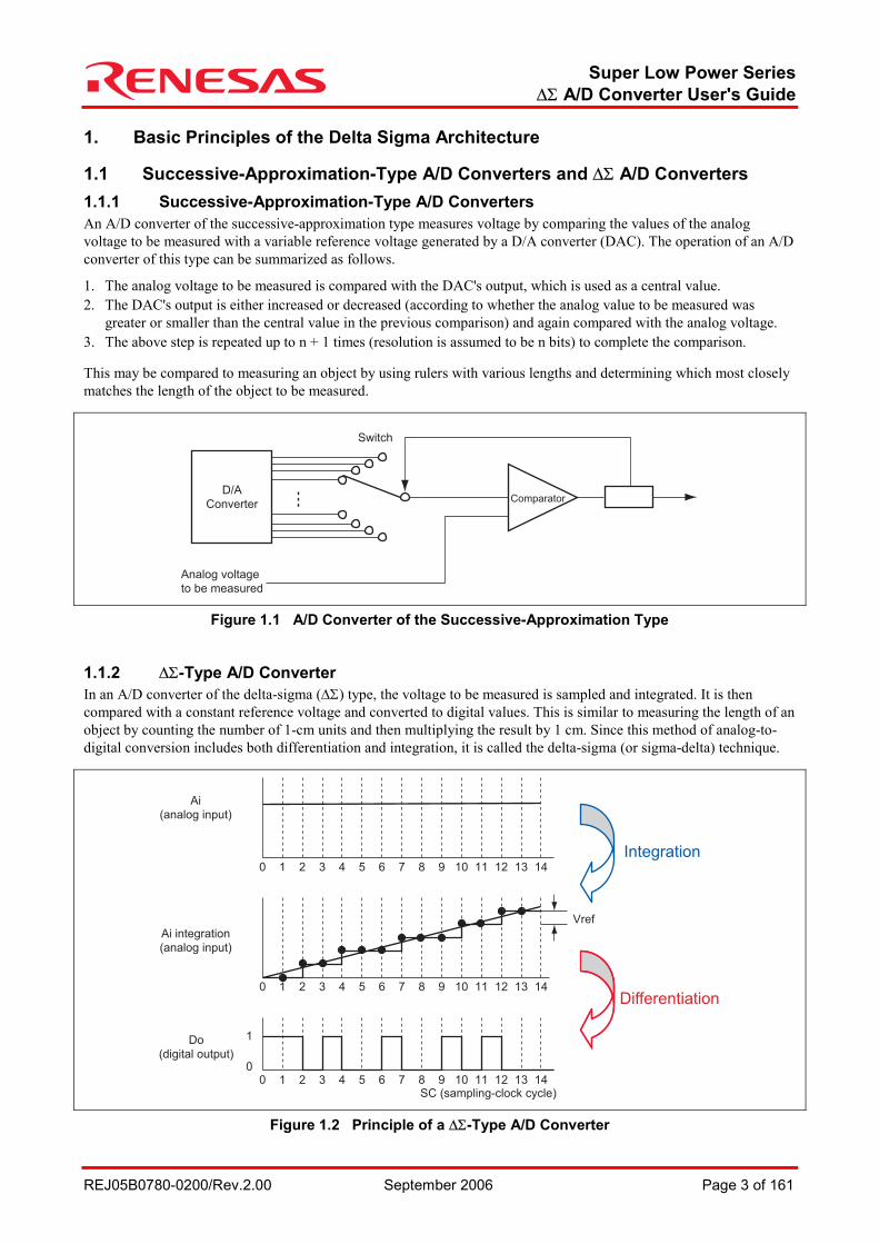
1.1 Successive-Approximation-Type A/D Converters and ∆Σ A/D Converters 1.1.1 Successive-Approximation-Type A/D Converters An A/D converter of the successive-approximation type measures voltage by comparing the values of the analog voltage to be measured with a variable reference voltage generated by a D/A converter (DAC). The operation of an A/D converter of this type can be summarized as follows.
1. The analog voltage to be measured is compared with the DAC's output, which is used as a central value. 2. The DAC's output is either increased or decreased (according to whether the analog value to be measured was
greater or smaller than the central value in the previous comparison) and again compared with the analog voltage. 3. The above step is repeated up to n + 1 times (resolution is assumed to be n bits) to complete the comparison. This may be compared to measuring an object by using rulers with various lengths and determining which most closely matches the length of the object to be measured.
D/A
ConverterComparator
Switch
Analog voltage
to be measured
Figure 1.1 A/D Converter of the Successive-Approximation Type
1.1.2 ∆Σ-Type A/D Converter In an A/D converter of the delta-sigma (∆Σ) type, the voltage to be measured is sampled and integrated. It is then compared with a constant reference voltage and converted to digital values. This is similar to measuring the length of an object by counting the number of 1-cm units and then multiplying the result by 1 cm. Since this method of analog-to-digital conversion includes both differentiation and integration, it is called the delta-sigma (or sigma-delta) technique.
0 1 2 3 4 5 6 7 8 9 10 11 12 13 14
Vref
Ai
(analog input)
Integration
Differentiation
Ai integration
(analog input)
Do
(digital output)
1
0
0 1 2 3 4 5 6 7 8 9 10 11 12 13 14
SC (sampling-clock cycle)0 1 2 3 4 5 6 7 8 9 10 11 12 13 14
Figure 1.2 Principle of a ∆Σ-Type A/D Converter
Super Low Power Series ∆Σ A/D Converter User's Guide
REJ05B0780-0200/Rev.2.00 September 2006 Page 4 of 161
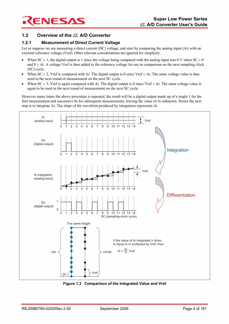
1.2 Overview of the ∆Σ A/D Converter 1.2.1 Measurement of Direct Current Voltage Let us suppose we are measuring a direct current (DC) voltage, and start by comparing the analog input (Ai) with an external reference voltage (Vref). Other relevant considerations are ignored for simplicity.
• When SC = 1, the digital output is 1 since the voltage being compared with the analog input was 0 V when SC = 0 and 0 < Ai. A voltage Vref is then added to the reference voltage for use in comparison on the next sampling clock (SC) cycle.
• When SC = 2, Vref is compared with Ai. The digital output is 0 since Vref > Ai. The same voltage value is thus used in the next round of measurement on the next SC cycle.
• When SC = 3, Vref is again compared with Ai. The digital output is 0 since Vref > Ai. The same voltage value is again to be used in the next round of measurement on the next SC cycle.
However many times the above procedure is repeated, the result will be a digital output made up of a single 1 for the first measurement and successive 0s for subsequent measurements, leaving the value of Ai unknown. Hence the next step is to integrate Ai. The slope of the waveform produced by integration represents Ai.
Ai
(analog input)
Integration
Differentiation
Ai integration
(analog input)
Do
(digital output)
Do
(digital output)
1
0
0 1 2 3 4 5 6 7 8 9 10 11 12 13 14
0 1 2 3 4 5 6 7 8 9 10 11 12 13 14
0 1 2 3 4 5 6 7 8 9 10 11 12 13 14
Vref
SC (sampling-clock cycle)0 1 2 3 4 5 6 7 8 9 10 11 12 13 14
Vref
mVrefnAi Ai = Vrefmn
VrefAi
The same height
If the value of Ai integrated n times
is equal to m multiplied by Vref, then
Figure 1.3 Comparison of the Integrated Value and Vref
Super Low Power Series ∆Σ A/D Converter User's Guide
REJ05B0780-0200/Rev.2.00 September 2006 Page 5 of 161
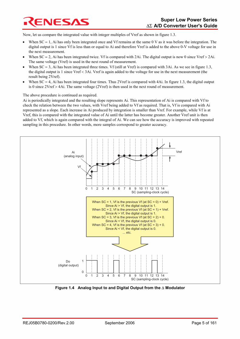
Now, let us compare the integrated value with integer multiples of Vref as shown in figure 1.3.
• When SC = 1, Ai has only been integrated once and Vf remains at the same 0 V as it was before the integration. The digital output is 1 since Vf is less than or equal to Ai and therefore Vref is added to the above 0-V voltage for use in the next measurement.
• When SC = 2, Ai has been integrated twice. Vf is compared with 2Ai. The digital output is now 0 since Vref > 2Ai. The same voltage (Vref) is used in the next round of measurement.
• When SC = 3, Ai has been integrated three times. Vf (still at Vref) is compared with 3Ai. As we see in figure 1.3, the digital output is 1 since Vref < 3Ai. Vref is again added to the voltage for use in the next measurement (the result being 2Vref).
• When SC = 4, Ai has been integrated four times. Thus 2Vref is compared with 4Ai. In figure 1.3, the digital output is 0 since 2Vref > 4Ai. The same voltage (2Vref) is then used in the next round of measurement.
The above procedure is continued as required. Ai is periodically integrated and the resulting slope represents Ai. This representation of Ai is compared with Vf to check the relation between the two values, with Vref being added to Vf as required. That is, Vf is compared with Ai represented as a slope. Each increase in Ai produced by integration is smaller than Vref. For example, while Vf is at Vref, this is compared with the integrated value of Ai until the latter has become greater. Another Vref unit is then added to Vf, which is again compared with the integral of Ai. We can see how the accuracy is improved with repeated sampling in this procedure. In other words, more samples correspond to greater accuracy.
Ai
(analog input)
Vref
Vf
Do
(digital output)
1
0
0 1 2 3 4 5 6 7 8 9 10 11 12 13 14SC (sampling-clock cycle)
0 1 2 3 4 5 6 7 8 9 10 11 12 13 14SC (sampling-clock cycle)
When SC = 1, Vf is the previous Vf (at SC = 0) + Vref.
Since Ai > Vf, the digital output is 1.
When SC = 2, Vf is the previous Vf (at SC = 1) + Vref.
Since Ai > Vf, the digital output is 1.
When SC = 3, Vf is the previous Vf (at SC = 2) + 0.
Since Ai < Vf, the digital output is 0.
When SC = 4, Vf is the previous Vf (at SC = 3) + 0.
Since Ai < Vf, the digital output is 0.
... etc.
Figure 1.4 Analog Input to and Digital Output from the ∆ Modulator
Super Low Power Series ∆Σ A/D Converter User's Guide
REJ05B0780-0200/Rev.2.00 September 2006 Page 6 of 161
1.3 Advantages of the ∆Σ A/D Converter 1.3.1 Successive-Approximation-Type A/D Converter • The speed of conversion is high and devices with lower resolutions are relatively cheap to implement. • Obtaining N bits of resolution requires the inclusion of 2n on-chip resistors. When the resistors are formed of silicon,
the accuracy is limited due to manufacturing dispersal. This approach is thus not suitable for high resolution. This limitation led to the need for a new method.
1.3.2 ∆Σ-Type A/D Converter • Converters of the ∆Σ type have lower conversion speeds than those of the successive-approximation type but higher
conversion speeds than converters of the double-integrating type. • This method is suitable for high resolution. Table 1.1 Comparison of Characteristics of Successive Approximation and ∆Σ Converters
Item Successive-Approximation Type ∆Σ Type Method Sample and hold Sampling Module size Large Fitting Conversion time Fast (approximately 10 µs
(H8S/2264) Slow (32 µs or more) (H8/38086R)
High resolution No Yes Frequency band Without constraint Depends on digital filter Noise immunity Low High (noise shaping)
Super Low Power Series ∆Σ A/D Converter User's Guide
REJ05B0780-0200/Rev.2.00 September 2006 Page 7 of 161
2. ∆Σ A/D Converter
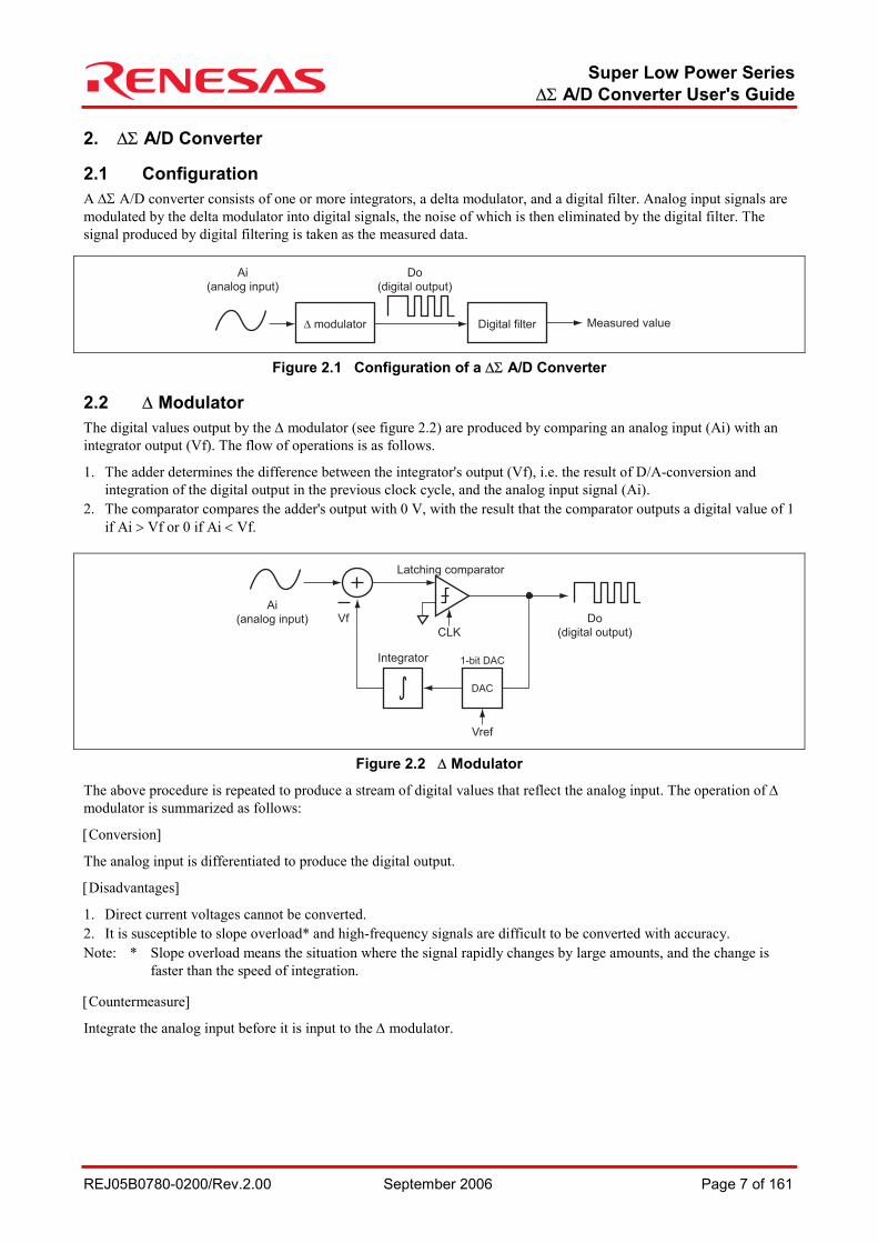
2.1 Configuration A ∆Σ A/D converter consists of one or more integrators, a delta modulator, and a digital filter. Analog input signals are modulated by the delta modulator into digital signals, the noise of which is then eliminated by the digital filter. The signal produced by digital filtering is taken as the measured data.
Do
(digital output)
Ai
(analog input)
∆ modulator Measured valueDigital filter
Figure 2.1 Configuration of a ∆Σ A/D Converter
2.2 ∆ Modulator The digital values output by the ∆ modulator (see figure 2.2) are produced by comparing an analog input (Ai) with an integrator output (Vf). The flow of operations is as follows.
1. The adder determines the difference between the integrator's output (Vf), i.e. the result of D/A-conversion and integration of the digital output in the previous clock cycle, and the analog input signal (Ai).
2. The comparator compares the adder's output with 0 V, with the result that the comparator outputs a digital value of 1 if Ai > Vf or 0 if Ai < Vf.
Ai
(analog input)CLK
Vref
Vf
DAC
1-bit DACIntegrator
Latching comparator
Do
(digital output)
Figure 2.2 ∆ Modulator
The above procedure is repeated to produce a stream of digital values that reflect the analog input. The operation of ∆ modulator is summarized as follows:
[Conversion]
The analog input is differentiated to produce the digital output.
[Disadvantages]
1. Direct current voltages cannot be converted. 2. It is susceptible to slope overload* and high-frequency signals are difficult to be converted with accuracy. Note: * Slope overload means the situation where the signal rapidly changes by large amounts, and the change is
faster than the speed of integration. [Countermeasure]
Integrate the analog input before it is input to the ∆ modulator.
Super Low Power Series ∆Σ A/D Converter User's Guide
REJ05B0780-0200/Rev.2.00 September 2006 Page 8 of 161
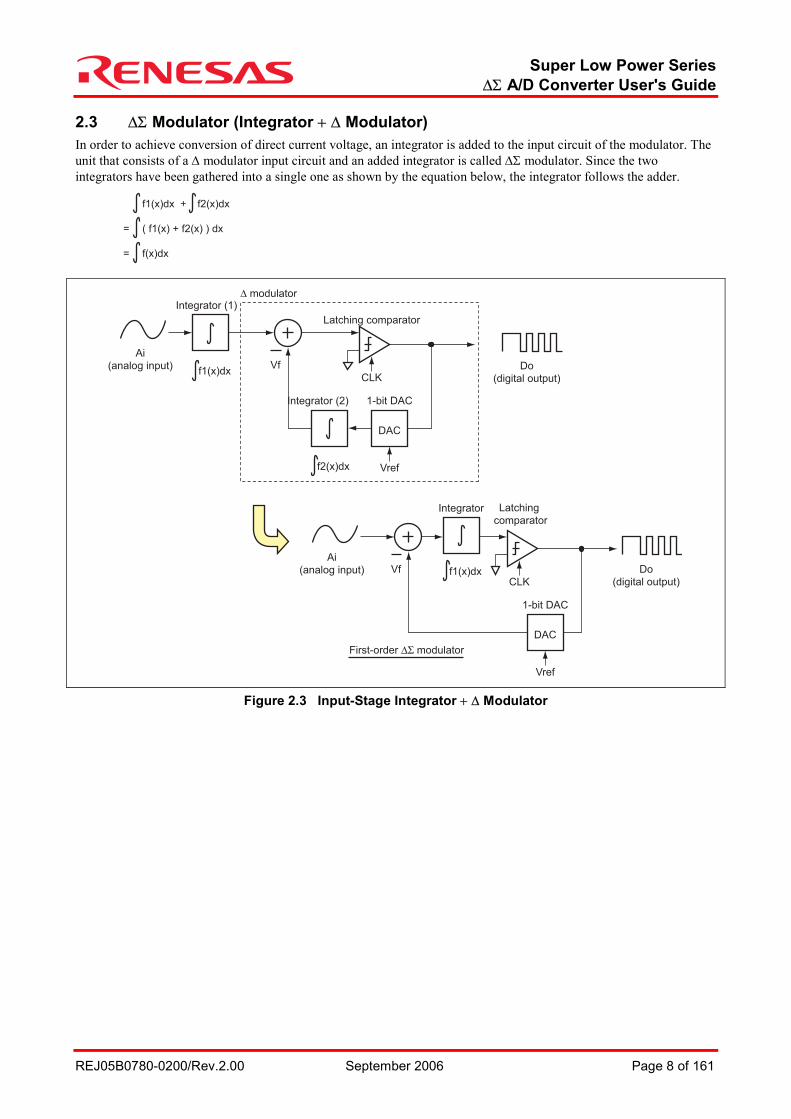
2.3 ∆Σ Modulator (Integrator + ∆ Modulator) In order to achieve conversion of direct current voltage, an integrator is added to the input circuit of the modulator. The unit that consists of a ∆ modulator input circuit and an added integrator is called ∆Σ modulator. Since the two integrators have been gathered into a single one as shown by the equation below, the integrator follows the adder.
f1(x)dx + f2(x)dx
= ( f1(x) + f2(x) ) dx
= f(x)dx
Ai
(analog input)CLK
Vref
Vf
DAC
1-bit DAC
f1(x)dx
f1(x)dx
f2(x)dx
Integrator (2)
Integrator (1)∆ modulator
Latching comparator
Ai
(analog input)
First-order ∆Σ modulator
CLK
Vref
Vf
DAC
1-bit DAC
Integrator Latching
comparator
Do
(digital output)
Do
(digital output)
Figure 2.3 Input-Stage Integrator + ∆ Modulator
Super Low Power Series ∆Σ A/D Converter User's Guide
REJ05B0780-0200/Rev.2.00 September 2006 Page 9 of 161
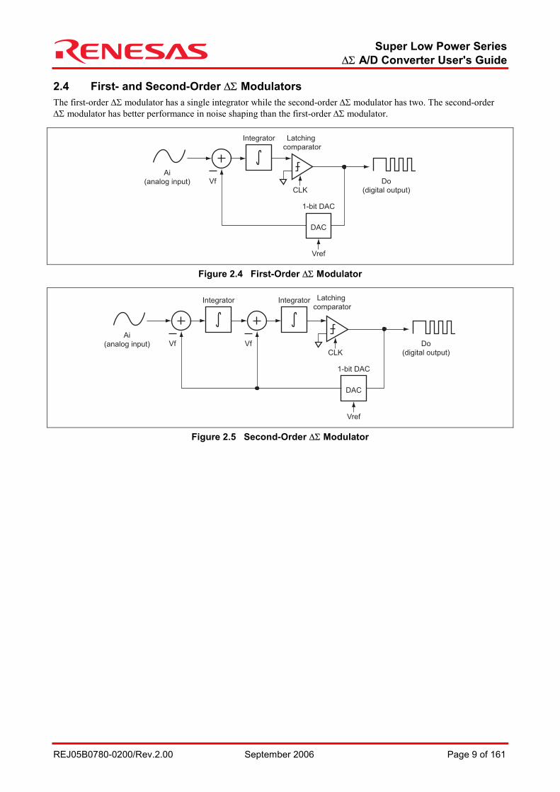
2.4 First- and Second-Order ∆Σ Modulators The first-order ∆Σ modulator has a single integrator while the second-order ∆Σ modulator has two. The second-order ∆Σ modulator has better performance in noise shaping than the first-order ∆Σ modulator.
Ai
(analog input)CLK
Vref
Vf
DAC
1-bit DAC
Integrator Latching
comparator
Do
(digital output)
Figure 2.4 First-Order ∆Σ Modulator
Ai
(analog input)CLK
Vref
Vf
DAC
1-bit DAC
IntegratorIntegrator Latching
comparator
Do
(digital output)
Vf
Figure 2.5 Second-Order ∆Σ Modulator
Super Low Power Series ∆Σ A/D Converter User's Guide
REJ05B0780-0200/Rev.2.00 September 2006 Page 10 of 161
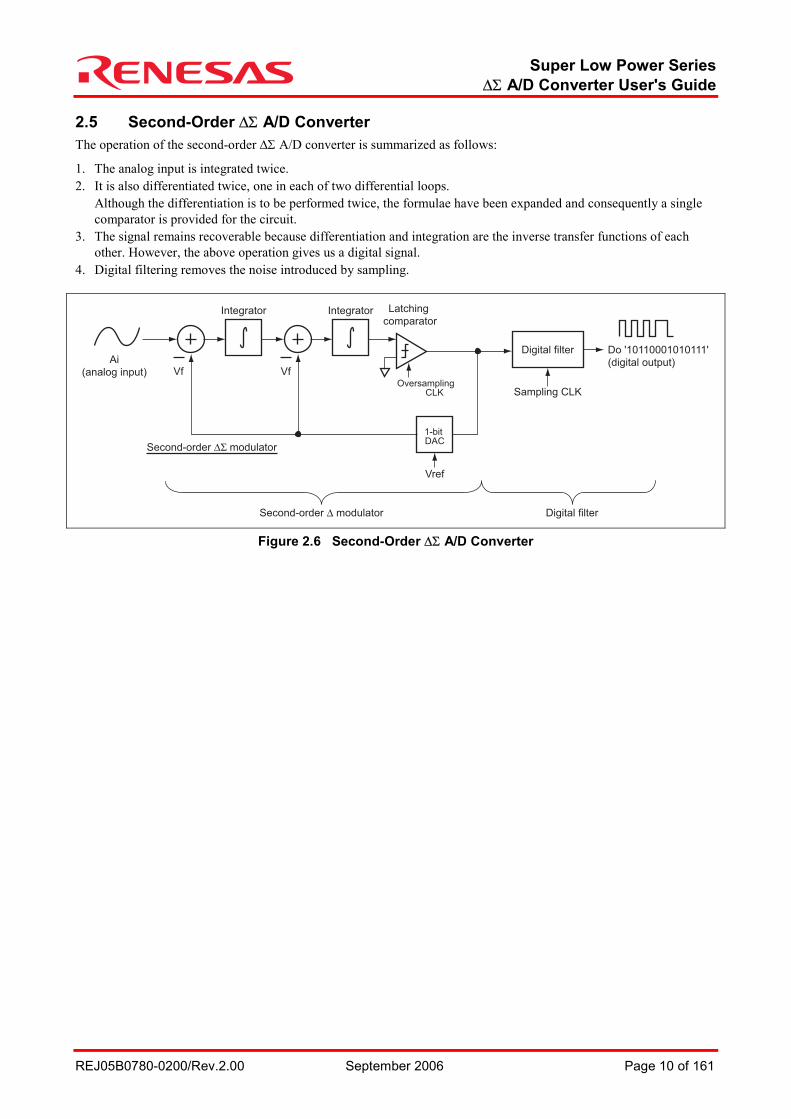
2.5 Second-Order ∆Σ A/D Converter The operation of the second-order ∆Σ A/D converter is summarized as follows:
1. The analog input is integrated twice. 2. It is also differentiated twice, one in each of two differential loops.
Although the differentiation is to be performed twice, the formulae have been expanded and consequently a single comparator is provided for the circuit.
3. The signal remains recoverable because differentiation and integration are the inverse transfer functions of each other. However, the above operation gives us a digital signal.
4. Digital filtering removes the noise introduced by sampling.
Second-order ∆ modulator Digital filter
Ai
(analog input)Oversampling CLK
Vref
Vf
1-bit DAC
IntegratorIntegrator Latching
comparator
Vf
Second-order ∆Σ modulator
Sampling CLK
Do '10110001010111'
(digital output)
Digital filter
Figure 2.6 Second-Order ∆Σ A/D Converter
Super Low Power Series ∆Σ A/D Converter User's Guide
REJ05B0780-0200/Rev.2.00 September 2006 Page 11 of 161
3. Filter
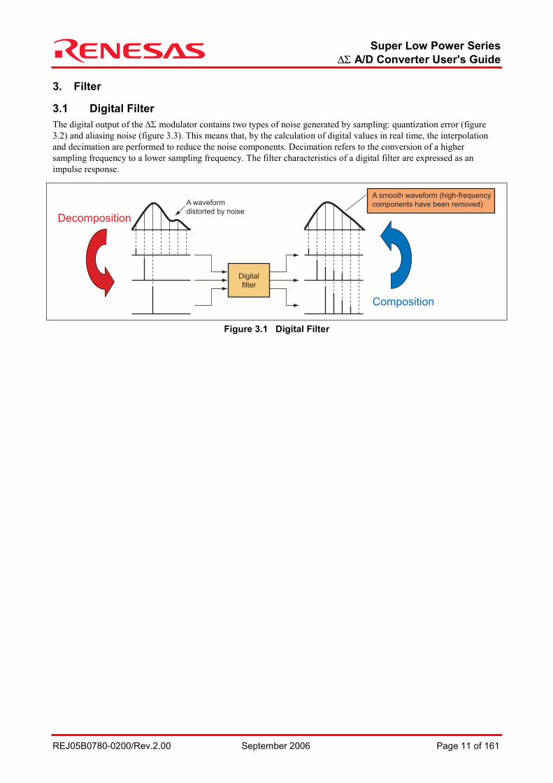
3.1 Digital Filter The digital output of the ∆Σ modulator contains two types of noise generated by sampling: quantization error (figure 3.2) and aliasing noise (figure 3.3). This means that, by the calculation of digital values in real time, the interpolation and decimation are performed to reduce the noise components. Decimation refers to the conversion of a higher sampling frequency to a lower sampling frequency. The filter characteristics of a digital filter are expressed as an impulse response.
Decomposition
Composition
A waveform
distorted by noise
A smooth waveform (high-frequency
components have been removed)
Digital
filter
Figure 3.1 Digital Filter
Super Low Power Series ∆Σ A/D Converter User's Guide
REJ05B0780-0200/Rev.2.00 September 2006 Page 12 of 161
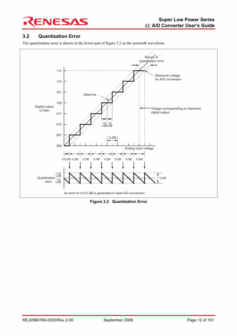
3.2 Quantization Error The quantization error is shown in the lower part of figure 3.2 as the sawtooth waveform.
Digital output
(3 bits)
1LSB
1LSB
1LSB1/2LSB 1LSB 1LSB 1LSB 1LSB 1LSB 1LSB
1/2LSB
1/2LSB
+1/2LSB
-1/2LSB
Range of
quantization error
Quantization
error
Maximum voltage
for A/D conversion
An error of ±1/2 LSB is generated in ideal A/D conversion.
Voltage corresponding to maximum
digital output
Analog input voltage
Ideal line
111
110
101
100
011
010
001
000
Figure 3.2 Quantization Error

Super Low Power Series ∆Σ A/D Converter User's Guide
REJ05B0780-0200/Rev.2.00 September 2006 Page 13 of 161
3.3 Aliasing Noise When analog signals f1 and f2 (f1 multiplied by 7) below are sampled at eight times the frequency of f1, the sampling points become identical with those that would be sampled from analog signal f2. The sampling points thus become a source for a component at frequency f2, and f2 is called the aliasing noise of f1 at the given sampling rate.
Analog signal f2
Analog signal f1
Analog signals
f1 & f2
fs = 8 × f1, f2 = 7 × f1
Interval at sampling
frequency fs
Sampling point
Figure 3.3 Aliasing Noise
Super Low Power Series ∆Σ A/D Converter User's Guide
REJ05B0780-0200/Rev.2.00 September 2006 Page 14 of 161
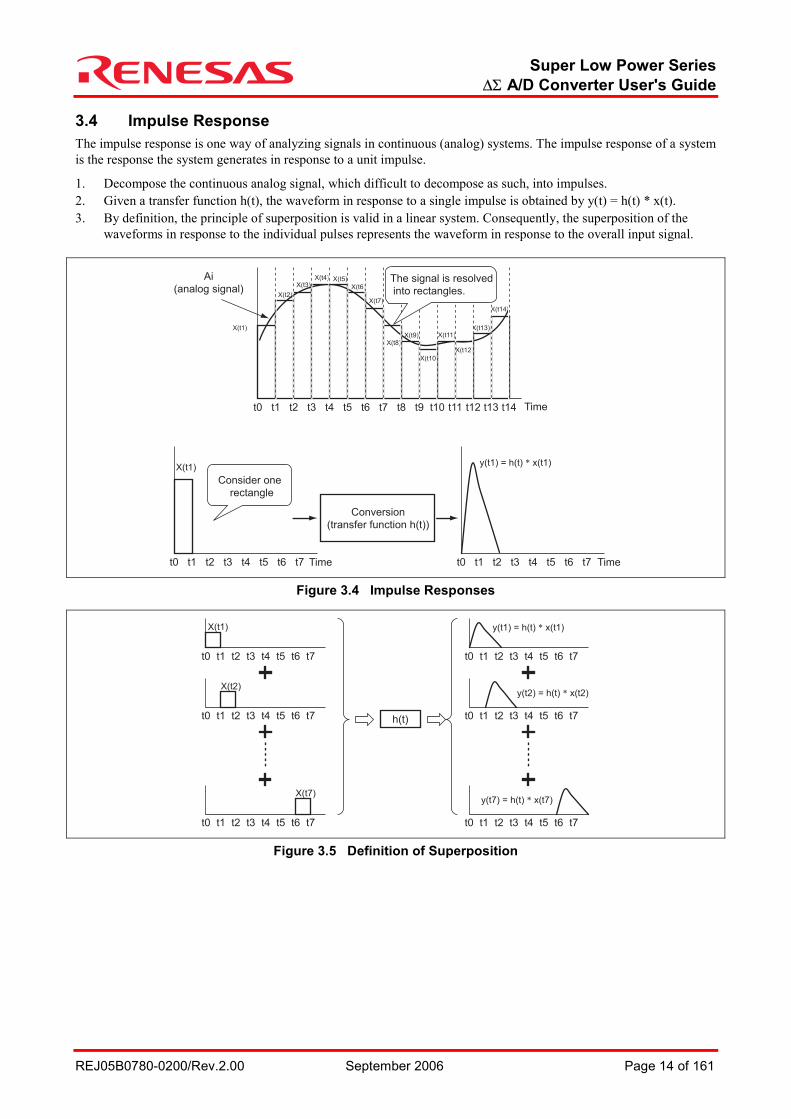
3.4 Impulse Response The impulse response is one way of analyzing signals in continuous (analog) systems. The impulse response of a system is the response the system generates in response to a unit impulse.
1. Decompose the continuous analog signal, which difficult to decompose as such, into impulses. 2. Given a transfer function h(t), the waveform in response to a single impulse is obtained by y(t) = h(t) * x(t). 3. By definition, the principle of superposition is valid in a linear system. Consequently, the superposition of the
waveforms in response to the individual pulses represents the waveform in response to the overall input signal.
Ai
(analog signal)
X(t1)
t0 t1 t2 t3 t4 t5 t6 t7
X(t1)
t0 t1 t2 t3 t4 t5 t6 t7
y(t1) = h(t) * x(t1)
t0 t1 t2 t3 t4 t5 t6 t7
t8 t9 t10 t11 t12 t13 t14
X(t2)
X(t3)X(t4) X(t5)
X(t6)
X(t7)
X(t8)X(t9)
X(t10)
X(t11)
X(t12)
X(t13)
X(t14)
The signal is resolved
into rectangles.
Consider one
rectangle
Conversion
(transfer function h(t))
Time
Time Time
Figure 3.4 Impulse Responses
h(t)
X(t1)
t0 t1 t2 t3 t4 t5 t6 t7
y(t1) = h(t) * x(t1)
t0 t1 t2 t3 t4 t5 t6 t7
X(t2)
t0 t1 t2 t3 t4 t5 t6 t7
y(t2) = h(t) * x(t2)
t0 t1 t2 t3 t4 t5 t6 t7
X(t7)
t0 t1 t2 t3 t4 t5 t6 t7
y(t7) = h(t) * x(t7)
t0 t1 t2 t3 t4 t5 t6 t7
Figure 3.5 Definition of Superposition
Super Low Power Series ∆Σ A/D Converter User's Guide
REJ05B0780-0200/Rev.2.00 September 2006 Page 15 of 161
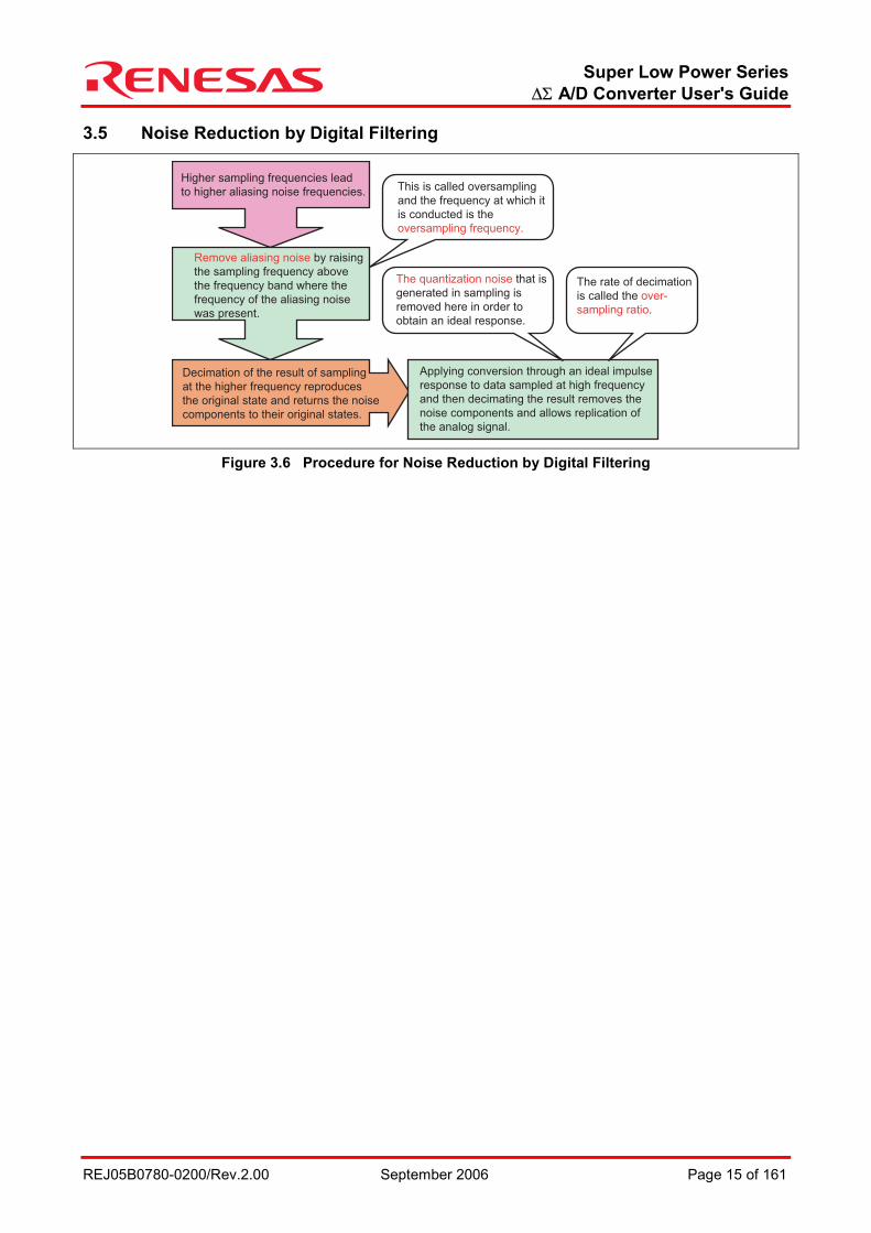
3.5 Noise Reduction by Digital Filtering
Higher sampling frequencies lead
to higher aliasing noise frequencies.
Remove aliasing noise by raising
the sampling frequency above
the frequency band where the
frequency of the aliasing noise
was present.
Decimation of the result of sampling
at the higher frequency reproduces
the original state and returns the noise
components to their original states.
This is called oversampling
and the frequency at which it
is conducted is the
oversampling frequency.
The quantization noise that is
generated in sampling is
removed here in order to
obtain an ideal response.
The rate of decimation
is called the over-
sampling ratio.
Applying conversion through an ideal impulse
response to data sampled at high frequency
and then decimating the result removes the
noise components and allows replication of
the analog signal.
Figure 3.6 Procedure for Noise Reduction by Digital Filtering
Super Low Power Series ∆Σ A/D Converter User's Guide
REJ05B0780-0200/Rev.2.00 September 2006 Page 16 of 161
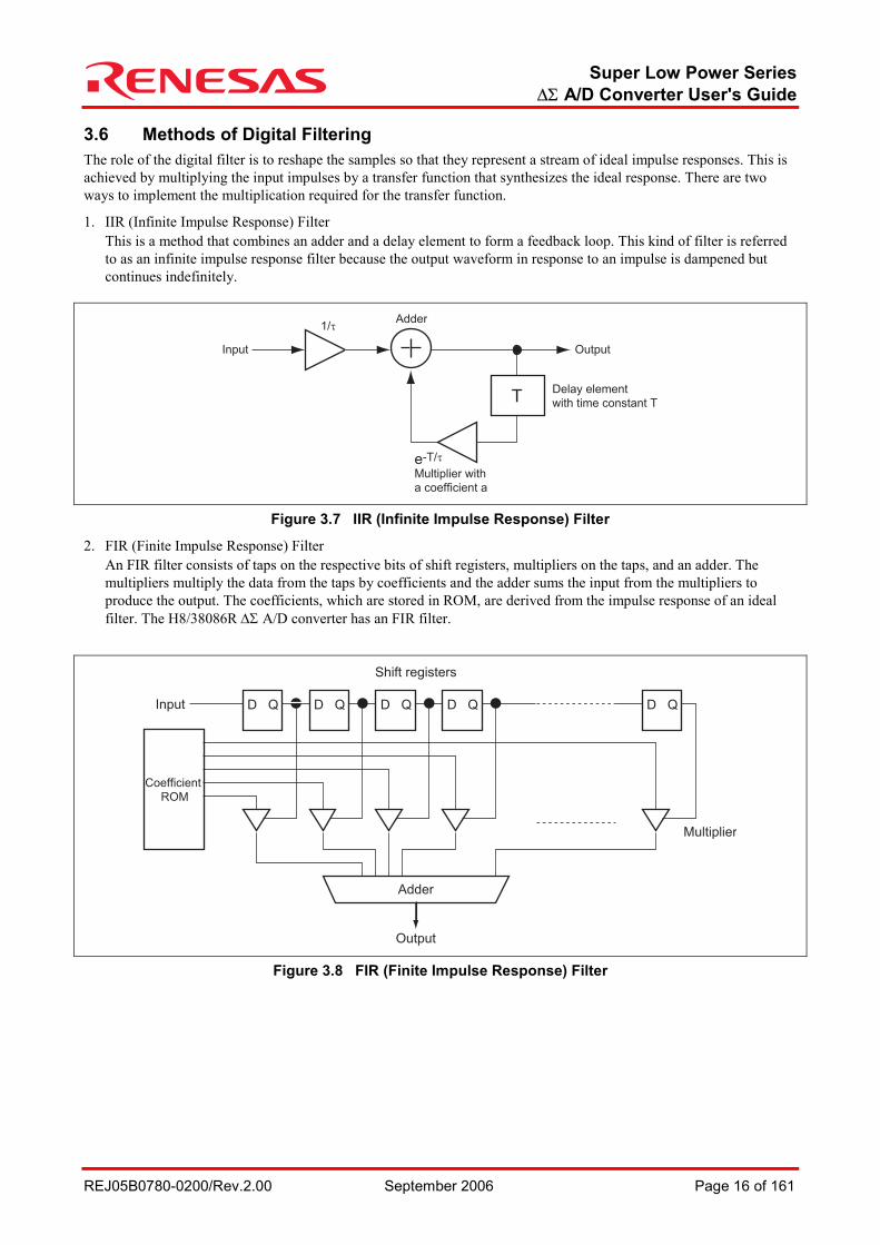
3.6 Methods of Digital Filtering The role of the digital filter is to reshape the samples so that they represent a stream of ideal impulse responses. This is achieved by multiplying the input impulses by a transfer function that synthesizes the ideal response. There are two ways to implement the multiplication required for the transfer function.
1. IIR (Infinite Impulse Response) Filter This is a method that combines an adder and a delay element to form a feedback loop. This kind of filter is referred to as an infinite impulse response filter because the output waveform in response to an impulse is dampened but continues indefinitely.
Input Output
Adder
TDelay element
with time constant T
Multiplier with
a coefficient a
1/τ
e-T/τ
Figure 3.7 IIR (Infinite Impulse Response) Filter
2. FIR (Finite Impulse Response) Filter An FIR filter consists of taps on the respective bits of shift registers, multipliers on the taps, and an adder. The multipliers multiply the data from the taps by coefficients and the adder sums the input from the multipliers to produce the output. The coefficients, which are stored in ROM, are derived from the impulse response of an ideal filter. The H8/38086R ∆Σ A/D converter has an FIR filter.
Output
Shift registers
Multiplier
Input D
Coefficient
ROM
Adder
Q D Q D Q D Q D Q
Figure 3.8 FIR (Finite Impulse Response) Filter
Super Low Power Series ∆Σ A/D Converter User's Guide
REJ05B0780-0200/Rev.2.00 September 2006 Page 17 of 161
4. Errors and Methods of Correction
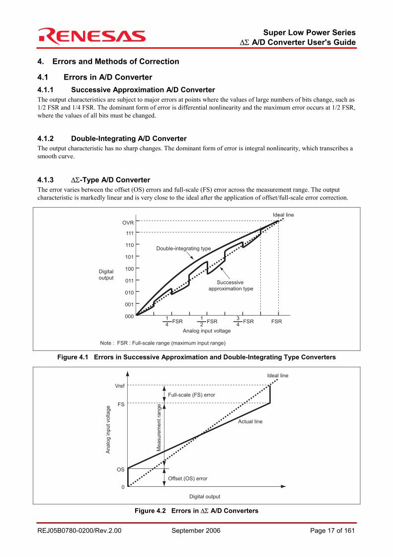
4.1 Errors in A/D Converter 4.1.1 Successive Approximation A/D Converter The output characteristics are subject to major errors at points where the values of large numbers of bits change, such as 1/2 FSR and 1/4 FSR. The dominant form of error is differential nonlinearity and the maximum error occurs at 1/2 FSR, where the values of all bits must be changed.
4.1.2 Double-Integrating A/D Converter The output characteristic has no sharp changes. The dominant form of error is integral nonlinearity, which transcribes a smooth curve.
4.1.3 ∆Σ-Type A/D Converter The error varies between the offset (OS) errors and full-scale (FS) error across the measurement range. The output characteristic is markedly linear and is very close to the ideal after the application of offset/full-scale error correction.
OVR
Digital
output
Analog input voltage
Note : FSR : Full-scale range (maximum input range)
Successive
approximation type
Double-integrating type
Ideal line
1
4FSR
111
110
101
100
011
010
001
000 1
2FSR
3
4FSR FSR
Figure 4.1 Errors in Successive Approximation and Double-Integrating Type Converters
Digital output
An
alo
g in
pu
t vo
lta
ge
Vref
FS
OS
Full-scale (FS) error
Me
asu
rem
en
t ra
ng
e
Actual line
Offset (OS) error
0
Ideal line
Figure 4.2 Errors in ∆Σ A/D Converters
Super Low Power Series ∆Σ A/D Converter User's Guide
REJ05B0780-0200/Rev.2.00 September 2006 Page 18 of 161
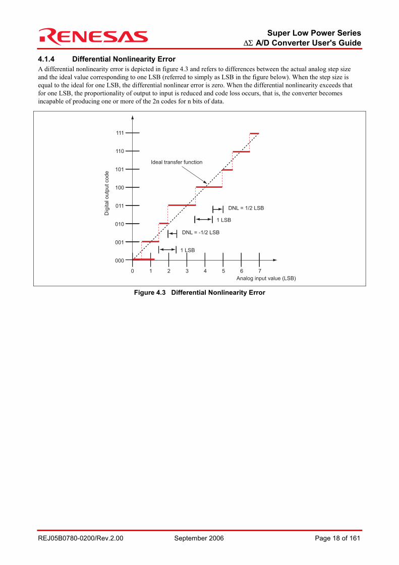
4.1.4 Differential Nonlinearity Error A differential nonlinearity error is depicted in figure 4.3 and refers to differences between the actual analog step size and the ideal value corresponding to one LSB (referred to simply as LSB in the figure below). When the step size is equal to the ideal for one LSB, the differential nonlinear error is zero. When the differential nonlinearity exceeds that for one LSB, the proportionality of output to input is reduced and code loss occurs, that is, the converter becomes incapable of producing one or more of the 2n codes for n bits of data.
Analog input value (LSB)
Dig
ital outp
ut
code
111
110
101
100
011
010
001
000
0 1 2 3 4 5 6 7
Ideal transfer function
DNL = 1/2 LSB
1 LSB
DNL = -1/2 LSB
1 LSB
Figure 4.3 Differential Nonlinearity Error
Super Low Power Series ∆Σ A/D Converter User's Guide
REJ05B0780-0200/Rev.2.00 September 2006 Page 19 of 161
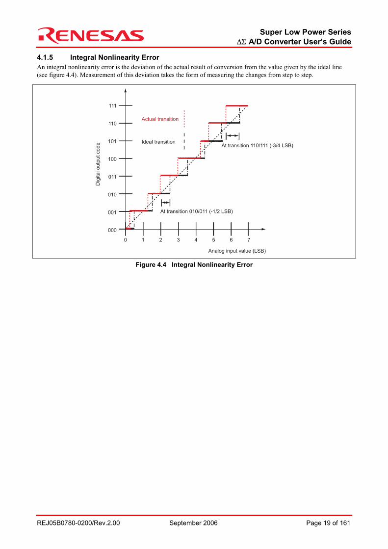
4.1.5 Integral Nonlinearity Error An integral nonlinearity error is the deviation of the actual result of conversion from the value given by the ideal line (see figure 4.4). Measurement of this deviation takes the form of measuring the changes from step to step.
Analog input value (LSB)
Dig
ital outp
ut
code
111
110
101
100
011
010
001
000
0 1 2 3 4 5 6 7
Ideal transition
Actual transition
At transition 110/111 (-3/4 LSB)
At transition 010/011 (-1/2 LSB)
Figure 4.4 Integral Nonlinearity Error

Super Low Power Series ∆Σ A/D Converter User's Guide
REJ05B0780-0200/Rev.2.00 September 2006 Page 20 of 161
4.2 Correction of Offset and Full-Scale Errors 4.2.1 Approach to Correction Figure 4.5 shows the relation between digital values (ADDR values) and analog values (to be measured) of the ∆Σ A/D converter.
The response of an ideal A/D converter, shown as a dashed line in figure 5.5, is linear from the origin to the full-scale voltage. However, the actual relation is portrayed by the solid line from the offset (OS) error to the full-scale (FS) error. Consequently, offset/full-scale error correction should be applied to derive more accurate values from the measured digital values.
Digital output (ADDR value)
Vref
xC
yB yC
xB
FS
OS
O
Offset (OS) error
Full-scale (FS) error
Ideal line
Converted value
(actual)
Me
asu
rem
en
t ra
ng
e
Analo
g input voltage
Figure 4.5 Relation of Analog Value (to be Measured) and Digital Value (ADDR Value)
The following equations describe the relations that define x and y values for the solid line.
lsb = (xC - xB) / (yC - yB) ···(1) x = (xC - xB) / (yC - yB) * y + OS ···(2) OS = xB - (xC - xB) / (yC - yB) * yB ···(3)
and from (1), (2), and (3), we have:
x = lsb * y + xB - lsb * yB = lsb * (y - yB) + xB
4.2.2 Correcting Offset and Full-Scale Errors The procedure for offset/full-scale error correction is as follows.
1. Determine x and y values at the four points A, B, C, and D shown in figure 4.5. 2. Calculate the slope (lsb) by determining x and y values at points B and C. 3. Calculate the target value from the digital value (the value in ADDR).
Measured value = Slope (lsb) * (ADDR value – yB) + xB
Super Low Power Series ∆Σ A/D Converter User's Guide
REJ05B0780-0200/Rev.2.00 September 2006 Page 21 of 161
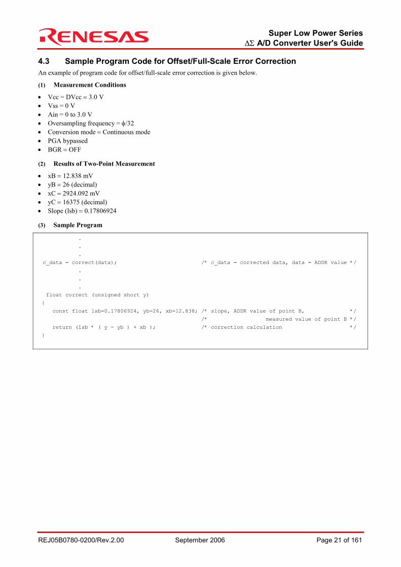
4.3 Sample Program Code for Offset/Full-Scale Error Correction An example of program code for offset/full-scale error correction is given below.
(1) Measurement Conditions
• Vcc = DVcc = 3.0 V • Vss = 0 V • Ain = 0 to 3.0 V • Oversampling frequency = φ/32 • Conversion mode = Continuous mode • PGA bypassed • BGR = OFF (2) Results of Two-Point Measurement
• xB = 12.838 mV • yB = 26 (decimal) • xC = 2924.092 mV • yC = 16375 (decimal) • Slope (lsb) = 0.17806924 (3) Sample Program
.
.
.
c_data = correct(data); /* c_data = corrected data, data = ADDR value */
.
.
.
float correct (unsigned short y)
const float lsb=0.17806924, yb=26, xb=12.838; /* slope, ADDR value of point B, */
/* measured value of point B */
return (lsb * ( y - yb ) + xb ); /* correction calculation */
Super Low Power Series ∆Σ A/D Converter User's Guide
REJ05B0780-0200/Rev.2.00 September 2006 Page 22 of 161
5. Recommended Usage Conditions and Usage Notes
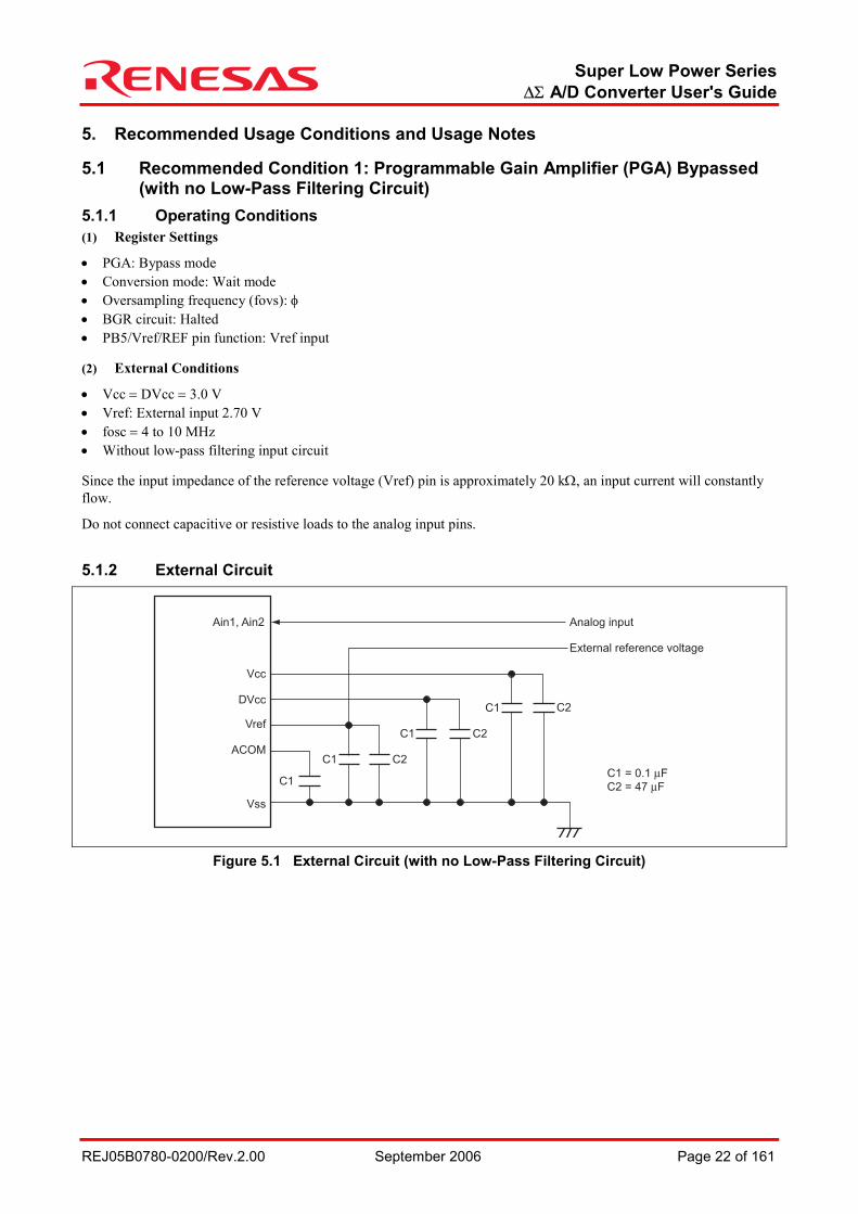
5.1 Recommended Condition 1: Programmable Gain Amplifier (PGA) Bypassed (with no Low-Pass Filtering Circuit)
5.1.1 Operating Conditions (1) Register Settings
• PGA: Bypass mode • Conversion mode: Wait mode • Oversampling frequency (fovs): φ • BGR circuit: Halted • PB5/Vref/REF pin function: Vref input (2) External Conditions
• Vcc = DVcc = 3.0 V • Vref: External input 2.70 V • fosc = 4 to 10 MHz • Without low-pass filtering input circuit Since the input impedance of the reference voltage (Vref) pin is approximately 20 kΩ, an input current will constantly flow.
Do not connect capacitive or resistive loads to the analog input pins.
5.1.2 External Circuit
Ain1, Ain2
Vcc
C1
C1
Vss
C1 = 0.1 µF
C2 = 47 µF
Analog input
External reference voltage
C2
C1 C2
C1 C2DVcc
Vref
ACOM
Figure 5.1 External Circuit (with no Low-Pass Filtering Circuit)
Super Low Power Series ∆Σ A/D Converter User's Guide
REJ05B0780-0200/Rev.2.00 September 2006 Page 23 of 161
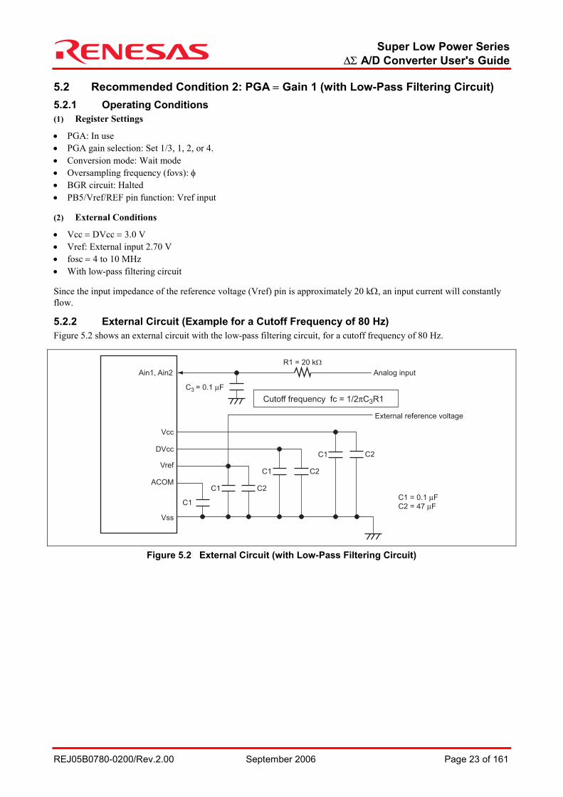
5.2 Recommended Condition 2: PGA = Gain 1 (with Low-Pass Filtering Circuit) 5.2.1 Operating Conditions (1) Register Settings
• PGA: In use • PGA gain selection: Set 1/3, 1, 2, or 4. • Conversion mode: Wait mode • Oversampling frequency (fovs): φ • BGR circuit: Halted • PB5/Vref/REF pin function: Vref input (2) External Conditions
• Vcc = DVcc = 3.0 V • Vref: External input 2.70 V • fosc = 4 to 10 MHz • With low-pass filtering circuit Since the input impedance of the reference voltage (Vref) pin is approximately 20 kΩ, an input current will constantly flow.
5.2.2 External Circuit (Example for a Cutoff Frequency of 80 Hz) Figure 5.2 shows an external circuit with the low-pass filtering circuit, for a cutoff frequency of 80 Hz.
Ain1, Ain2
Vcc
C1
C1
Vss
C1 = 0.1 µF
C2 = 47 µF
Analog input
External reference voltage
C3 = 0.1 µF
R1 = 20 kΩ
C2
C1 C2
C1 C2DVcc
Vref
ACOM
Cutoff frequency fc = 1/2πC3R1
Figure 5.2 External Circuit (with Low-Pass Filtering Circuit)
Super Low Power Series ∆Σ A/D Converter User's Guide
REJ05B0780-0200/Rev.2.00 September 2006 Page 24 of 161
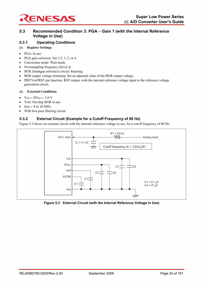
5.3 Recommended Condition 3: PGA = Gain 1 (with the Internal Reference Voltage in Use)
5.3.1 Operating Conditions (1) Register Settings
• PGA: In use • PGA gain selection: Set 1/3, 1, 2, or 4. • Conversion mode: Wait mode • Oversampling frequency (fovs): φ • BGR (bandgap reference) circuit: Running • BGR output voltage trimming: Set an adjusted value of the BGR output voltage. • PB5/Vref/REF pin function: REF output, with the internal reference voltage input to the reference voltage
generation circuit. (2) External Conditions
• Vcc = DVcc = 3.0 V • Vref: On-chip BGR in use • fosc = 4 to 10 MHz • With low-pass filtering circuit 5.3.2 External Circuit (Example for a Cutoff Frequency of 80 Hz) Figure 5.3 shows an external circuit with the internal reference voltage in use, for a cutoff frequency of 80 Hz.
Ain1, Ain2
Vcc
C1
C1
Vss
C1 = 0.1 µF
C2 = 47 µF
Analog input
C3 = 0.1 µF
R1 = 20 kΩ
C1 C2
C1 C2DVcc
Vref
ACOM
Cutoff frequency fc = 1/2πC3R1
Figure 5.3 External Circuit (with the Internal Reference Voltage in Use)
Super Low Power Series ∆Σ A/D Converter User's Guide
REJ05B0780-0200/Rev.2.00 September 2006 Page 25 of 161
5.4 Usage Notes This subsection provides information on precautions to take to ensure accurate operation of the A/D converter.
5.4.1 Reduction of Internally Generated Noise After the start of A/D conversion, place the chip in sleep mode to reduce noise generation by the CPU. As far as is possible, do not use any other peripheral functionality while A/D conversion is in progress.
5.4.2 Regarding the Oversampling Frequency When the oversampling frequency has been divided, noise produced by peripheral I/O affects the converter. Consequently, do not use frequency division in normal A/D conversion.
5.4.3 Note on Large Potential Differences between the Input Pins (Ain1 and Ain2) When the potential difference between input pins Ain1 and Ain2 is large, convergence on the voltage values can take time if measurement is attempted with switching between these two pins. In this case, discard the first value to be measured and use the data from the second measurement onwards.
5.4.4 Measurement when Power is Initially Supplied Charging of the capacitor in the input circuit when power is initially supplied can take a little time. In this case, discard the first value to be measured and use the data from the second measurement onwards.
5.4.5 Averaging Since errors in A/D conversion can be reduced by increasing the number of rounds of measurement and averaging the results, averaging across multiple rounds of measurement is strongly recommended where the extension of the processing time does not become a problem.
5.4.6 Treatment of the Internal Reference Voltage (REF) (1) Adjustment of the Internal Reference Voltage
The internal reference value (typ.) is 1.17 V. Measure the value and, if necessary, adjust it before use. Adjustment of the output voltage is controlled by bits 2 to 0 in the BGR control register (BGRMR).
(2) External Use of the Internal Reference Voltage
The REF voltage output is incapable of driving sufficient current for external use. If the REF voltage is to be used externally, include an element that has a high input impedance (operational amplifier, etc.) to amplify the current.
5.4.7 Board Design As a measure against noise, use a multilayered board having separate Vcc and GND layers and prevent the superposition of noise on input lines.
5.4.8 Input Impedance when the PGA is Bypassed (1) When the PGA is in Use
Since the input impedance of the programmable gain amplifier is large, an analog filter (a circuit with time constant set by CR elements) can be used.
(2) When the PGA is Bypassed
When the A/D conversion time is 32 µs, each kΩ of input resistance produces a voltage drop of approximately 5.6 mV. Since this voltage is smaller with a longer conversion time, be sure to take this point into consideration as a worst-case condition in the design process.
Super Low Power Series ∆Σ A/D Converter User's Guide
REJ05B0780-0200/Rev.2.00 September 2006 Page 26 of 161
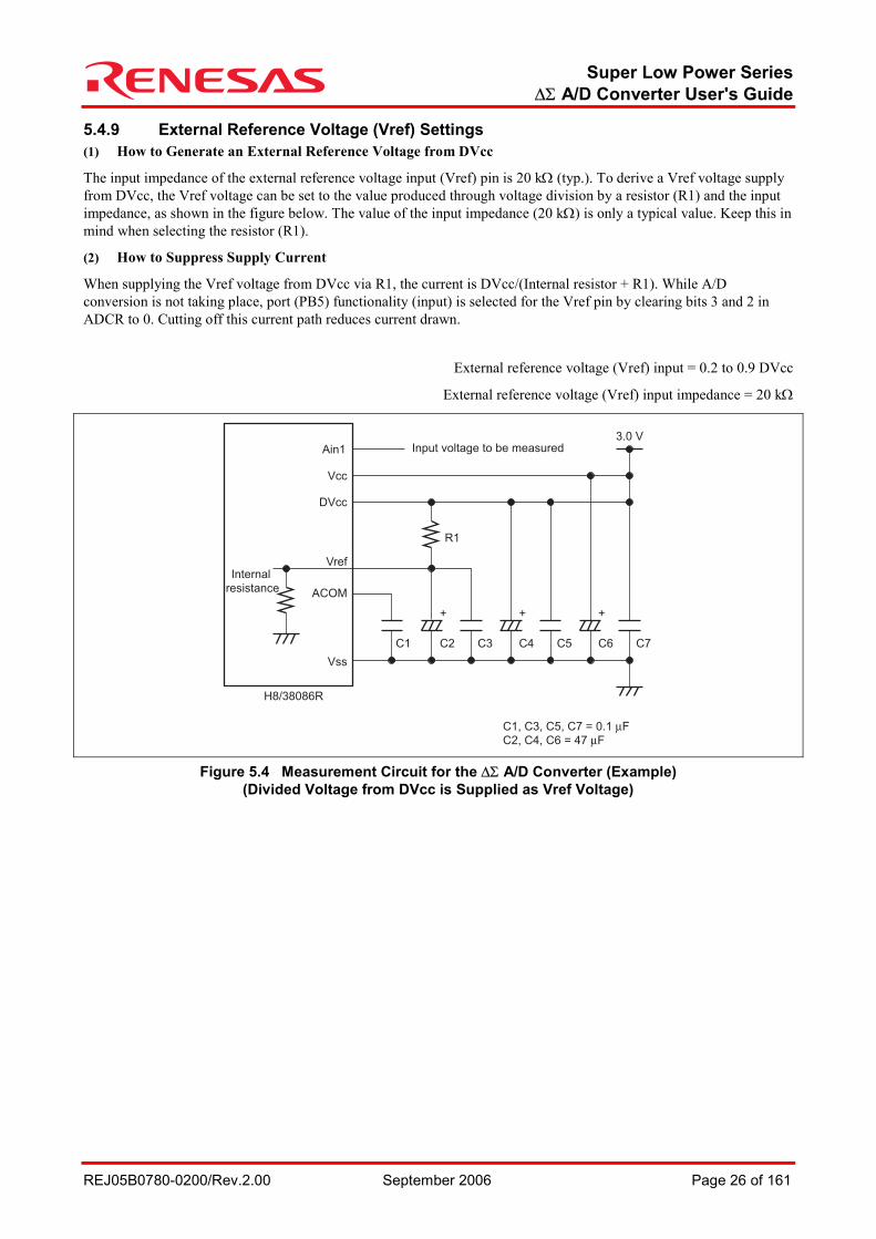
5.4.9 External Reference Voltage (Vref) Settings (1) How to Generate an External Reference Voltage from DVcc
The input impedance of the external reference voltage input (Vref) pin is 20 kΩ (typ.). To derive a Vref voltage supply from DVcc, the Vref voltage can be set to the value produced through voltage division by a resistor (R1) and the input impedance, as shown in the figure below. The value of the input impedance (20 kΩ) is only a typical value. Keep this in mind when selecting the resistor (R1).
(2) How to Suppress Supply Current
When supplying the Vref voltage from DVcc via R1, the current is DVcc/(Internal resistor + R1). While A/D conversion is not taking place, port (PB5) functionality (input) is selected for the Vref pin by clearing bits 3 and 2 in ADCR to 0. Cutting off this current path reduces current drawn.
External reference voltage (Vref) input = 0.2 to 0.9 DVcc
External reference voltage (Vref) input impedance = 20 kΩ
Ain1
Vcc
C1 C2
R1
+
Vss
H8/38086R
C1, C3, C5, C7 = 0.1 µF
C2, C4, C6 = 47 µF
Input voltage to be measured
C3 C4
+
C5 C6
+
C7
3.0 V
DVcc
Vref
ACOM
Internal
resistance
Figure 5.4 Measurement Circuit for the ∆Σ A/D Converter (Example) (Divided Voltage from DVcc is Supplied as Vref Voltage)

Super Low Power Series ∆Σ A/D Converter User's Guide
REJ05B0780-0200/Rev.2.00 September 2006 Page 27 of 161
6. Application Notes
6.1 Voltage Measurement Using the ∆Σ A/D Converter when an External Reference Voltage Used
6.1.1 Specifications • As is shown in figure 6.1, the internal ∆Σ A/D converter of the H8/38086R is used to measure the voltage input to
the Ain pin. • An external input voltage provides the reference voltage for the ∆Σ A/D converter. • The voltage on the Ain1 pin is measured, that is, converted from an analog level to a digital value, and the result of
A/D conversion is stored in the internal RAM. A/D conversion is performed twice, with the result of the first conversion being discarded. Only the results of the second conversion are stored. Offset and full-scale errors in the 14-bit results of A/D conversion read-out from the A/D Data Register (ADDR) are corrected before the data is stored.
• A/D conversion is performed in the following operating mode: conversion is in the wait mode, the oversampling frequency is φ, and the programmable gain amplifier (PGA) is bypassed.
• The device is placed in sleep (high-speed) mode during A/D conversion, since this reduces the noise generated by the CPU and other modules. On generation of the A/D-conversion-complete interrupt, the device makes the transition from sleep mode to active (high-speed) mode; correction is applied and then the results of A/D conversion are stored in the internal RAM. The module-standby function is used to place all internal peripheral modules other than the ∆Σ A/D converter (i.e. the SCI modules, successive approximation A/D converter, timer F, RTC, TPU, IIC2, PWM, AEC, watchdog timer, and LCD controller/driver) in the module-standby mode.
Vref
Ain1
H8/38086R
External reference voltage
Input of the voltage to be measured
Figure 6.1 Configuration for Voltage Measurement by the ∆Σ A/D Converter (with an External Reference Voltage in Use)
Super Low Power Series ∆Σ A/D Converter User's Guide
REJ05B0780-0200/Rev.2.00 September 2006 Page 28 of 161
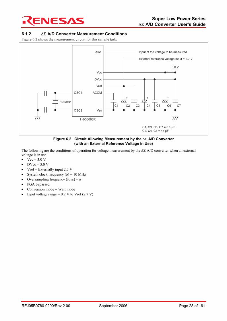
6.1.2 ∆Σ A/D Converter Measurement Conditions Figure 6.2 shows the measurement circuit for this sample task.
Ain1
Vcc
C1 C2
+
Vss
H8/38086R
External reference voltage input = 2.7 V
C1, C3, C5, C7 = 0.1 µF
C2, C4, C6 = 47 µF
Input of the voltage to be measured
C3 C4
+
C5 C6
+
C7
3.0 V
10 MHz
DVcc
Vref
ACOM
OSC2
OSC1
Figure 6.2 Circuit Allowing Measurement by the ∆Σ A/D Converter (with an External Reference Voltage in Use)
The following are the conditions of operation for voltage measurement by the ∆Σ A/D converter when an external voltage is in use. • Vcc = 3.0 V • DVcc = 3.0 V • Vref = Externally input 2.7 V • System clock frequency (φ) = 10 MHz • Oversampling frequency (fovs) = φ • PGA bypassed • Conversion mode = Wait mode • Input voltage range = 0.2 V to Vref (2.7 V)
Super Low Power Series ∆Σ A/D Converter User's Guide
REJ05B0780-0200/Rev.2.00 September 2006 Page 29 of 161
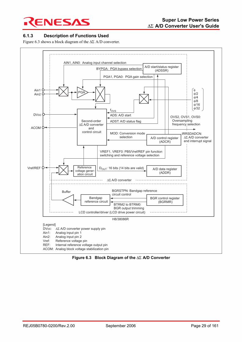
6.1.3 Description of Functions Used Figure 6.3 shows a block diagram of the ∆Σ A/D converter.
Ain1
Ain2
DVcc
ACOM
PGA
Buffer
A/D start/status register(ADSSR)
Second-order ∆Σ A/D converter
and control circuit
Reference voltage gener-
ation circuit
A/D control register (ADCR)
BGR control register (BGRMR)
Bandgap reference circuit
A/D data register(ADDR)
LCD controller/driver (LCD drive power circuit)
H8/38086R
∆Σ A/D converter
BGRSTPN: Bandgap reference circuit control
BTRM2 to BTRM0:BGR output trimming
VREF1, VREF0: PB5/Vref/REF pin function switching and reference voltage selection
MOD: Conversion mode selection
DOUT: 16 bits (14 bits are valid)
ADST: A/D status flag
ADS: A/D start
fOVS
OVS2, OVS1, OVS0:Oversampling frequency selection
PGA1, PGA0: PGA gain selection
BYPGA: PGA bypass selection
AIN1, AIN0: Analog input channel selection
Vref/REF
φφ/2φ/4φ/8φ/16φ/32
[Legend]
DVcc: ∆Σ A/D converter power supply pin
Ain1: Analog input pin 1
Ain2: Analog input pin 2
Vref: Reference voltage pin
REF: Internal reference voltage output pin
ACOM: Analog block voltage stabilization pin
IRRSDADCN:∆Σ A/D converter end interrupt signal
Figure 6.3 Block Diagram of the ∆Σ A/D Converter
Super Low Power Series ∆Σ A/D Converter User's Guide
REJ05B0780-0200/Rev.2.00 September 2006 Page 30 of 161
The characteristics and features of the ∆Σ A/D converter are described below.
(1) Features
• Resolution: 14 bits • Number of input channels: 2 • Conversion method: Second-order ∆Σ, 320-times oversampling • Conversion time: 32 µs per channel (in operation at 10 MHz) • Number of interrupt sources: 1 (A/D conversion-complete interrupt request) • Module standby mode for individual modules means that modules that are not in use can be placed in standby mode
while ∆Σ A/D conversion is in progress. (2) Input/Output Pins
The pins used with the ∆Σ A/D converter are described in table 6.1. Table 6.1 ∆Σ A/D Converter Pins
Pin Name Symbol I/O Function Reference voltage pin Vref Input External reference voltage input Internal reference voltage output pin REF Output Internal reference voltage output Analog block voltage stabilization pin ACOM Output Provides stabilization when
connected to a capacitor with a value of 0.1 µF
Analog input pin 1 Ain1 Input Analog input pin Analog input pin 2 Ain2 Input Analog input pin ∆Σ A/D converter analog power supply pin DVcc Input Power supply pin (3) Internal Registers
The registers of the ∆Σ A/D converter are listed below. • A/D Data Register (ADDR)
ADDR is a 16-bit read-only register that holds the result of A/D conversion. ADDR is always readable by the CPU. The value in ADDR is undefined during A/D conversion. After conversion, the 14 higher-order bits of ADDR holds the fourteen bits of converted data. ADDR retains this data until the next round of conversion is started. The initial value in ADDR is undefined.
• BGR Control Register (BGRMR) BGRMR controls operation of the bandgap reference circuit (BGR) and is used to adjust the internal reference voltage (BGR output voltage) output on the REF pin.
• A/D Control Register (ADCR) ADCR is used to set the conversion mode, the multiplier for the PGA (programmable gain amplifier), the function of pin PB5/Vref/REF, the reference voltage, and the oversampling frequency.
• A/D Start/Status Register (ADSSR) ADSSR contains the A/D conversion status flag, and is used to select the analog input channel and the PGA bypass mode.
(4) ∆Σ A/D Converter
In the ∆Σ A/D converter, a ∆Σ modulator is applied to convert analog input voltages in the range determined by the voltage on the Vref pin to digital values with a resolution of 14 bits. The converter consists of an analog block, the main component of which is the ∆Σ modulator, and a digital block based on a digital filtering control circuit. In the analog block, the voltages from analog input pins 1 and 2 (Ain1 and Ain2) are sampled at a frequency 320 times that of the conversion cycle (oversampling frequency), and then converted to a stream of 1-bit digital values by the second-order ∆Σ modulator. The result of this conversion process is passed through the decimation filter in the digital block, which produces the 14-bit unsigned binary output that is placed in the A/D Data Register (ADDR). In the ADDR, bit 13 is the MSB (most significant bit) and bit 0 the LSB (least significant bit).

Super Low Power Series ∆Σ A/D Converter User's Guide
REJ05B0780-0200/Rev.2.00 September 2006 Page 31 of 161
(5) Conversion Modes of the ∆Σ A/D Converter
The ∆Σ A/D converter supports two conversion modes: wait mode and continuous mode. (a) Wait Mode
In the wait mode, A/D conversion of the analog input on the specified channel is performed once in the following sequence.
1. When the ADS bit of the A/D Start/Status Register (ADSSR) is set to 1 by software, A/D conversion of the analog input on the specified channel starts.
2. On completion of A/D conversion, the result is transferred to the A/D Data Register (ADDR). 3. The A/D converter interrupt request flag (IRRSAD) of Interrupt Request Register 2 (IRR2) is set to 1. At this point,
if the A/D Converter Interrupt Request Enable bit (IENSAD) of Interrupt Enable Register 2 (IENR2) is 1, an A/D conversion-complete interrupt request is also generated.
4. The ADST bit is held at 1 during A/D conversion and then automatically cleared to 0 when the conversion is finished. The A/D converter then enters the wait state.
(b) Continuous Mode
In the continuous mode, continuous A/D conversion of the analog input on the specified channel is performed in the following sequence.
1. When the MOD bit of the A/D Control Register (ADCR) is set to 1 by software, A/D conversion of the analog input on the specified channel starts.
2. On completion of A/D conversion, the result is transferred to the A/D Data Register (ADDR). 3. The A/D converter interrupt request flag (IRRSAD) of Interrupt Request Register 2 (IRR2) is set to 1. At this point,
if the A/D Converter Interrupt Request Enable bit (IENSAD) of Interrupt Enable Register 2 (IENR2) is 1, an A/D conversion-complete interrupt request is also generated.
4. Steps 2 and 3 are repeated. The converter is taken out of the continuous mode by placing it in the watch mode, sub-active mode, sub-sleep mode, or standby mode, or by clearing the MOD bit of the ADCR register to 0.

Super Low Power Series ∆Σ A/D Converter User's Guide
REJ05B0780-0200/Rev.2.00 September 2006 Page 32 of 161
(6) ∆Σ A/D Converter Registers and Modes of Operation
The states of the registers of the ∆Σ A/D converter in the various MCU operating modes and in module-standby mode are as listed in table 6.2.
Table 6.2 Operating Modes and the ∆Σ A/D Converter
Operating Mode
On a Reset Active Sleep Watch Sub-Active
Sub-Sleep Standby
Module Standby
ADCR register
Reset Operational Retained Retained Retained Retained Retained Retained
ADSSR register
Reset Operational Operational Retained Retained Retained Retained Retained
ADDR register
Retained* Operational Operational Retained Retained Retained Retained Retained
BGRMR register
Reset Operational Retained Retained Operational Retained Retained Retained
Note: * The value is undefined after a power-on reset. (7) Pin Assignments
Pin assignments in this sample task are listed in table 6.3. Table 6.3 Assignment of Functions
Pin Name Description Vref/REF Vref, input for the external reference voltage at 2.7 VDC DVcc Input for the 3.0 VDC analog power supply for the ∆Σ A/D converter Ain1 Analog input for the value to be measured Ain2 Not used ACOM Analog-block voltage-stabilization pin for connection to a 0.1-µF capacitor
Super Low Power Series ∆Σ A/D Converter User's Guide
REJ05B0780-0200/Rev.2.00 September 2006 Page 33 of 161
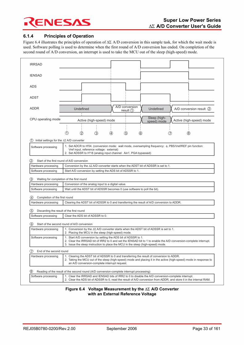
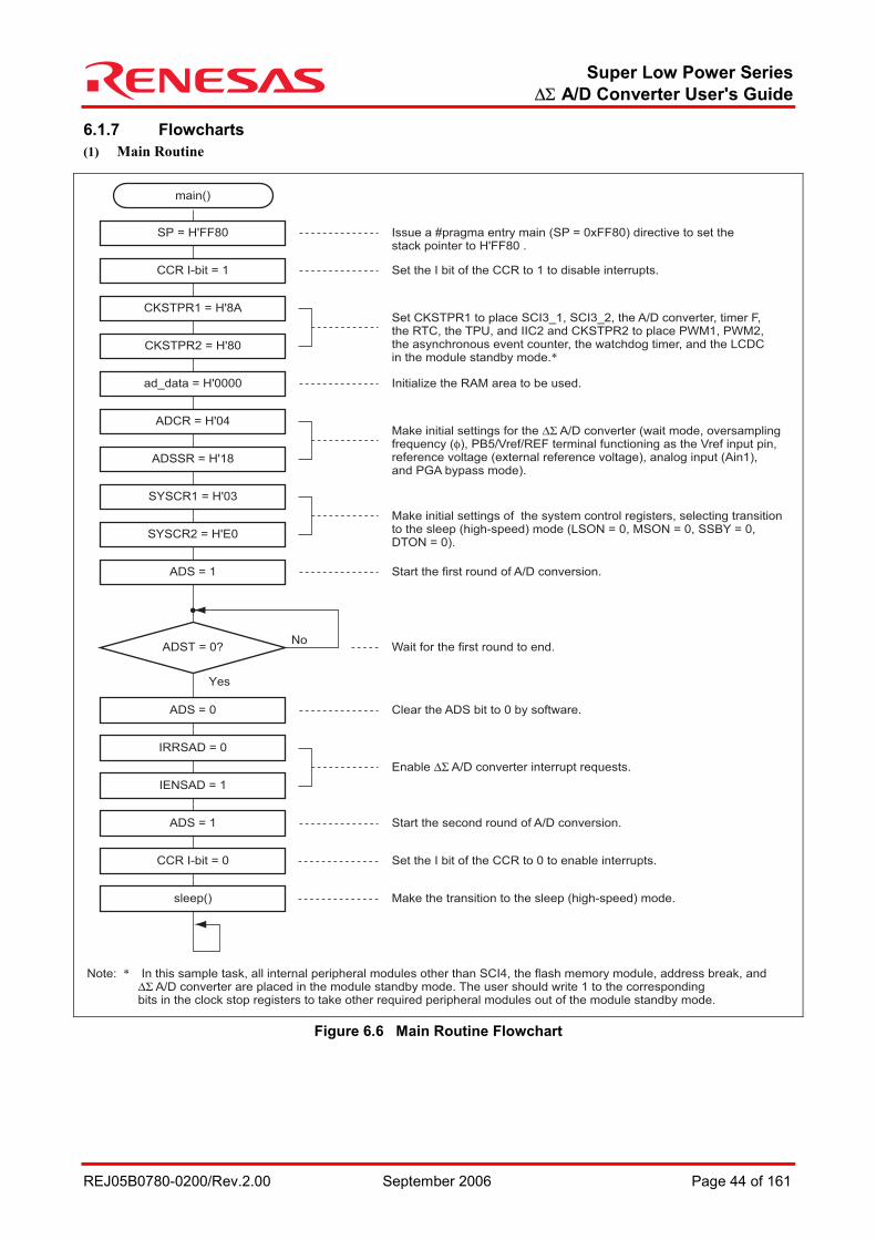
6.1.4 Principles of Operation Figure 6.4 illustrates the principles of operation of ∆Σ A/D conversion in this sample task, for which the wait mode is used. Software polling is used to determine when the first round of A/D conversion has ended. On completion of the second round of A/D conversion, an interrupt is used to take the MCU out of the sleep (high-speed) mode.
Active (high-speed) mode
IRRSAD
IENSAD
ADS
ADST
ADDR
CPU operating mode Sleep (high-speed) mode
Initial settings for the ∆Σ A/D converter
Software processing 1. Set ADCR to H'04. (conversion mode: wait mode, oversampling frequency: φ, PB5/Vref/REF pin function:
Vref input, reference voltage: external)
2. Set ADSSR to H'18 (analog input channel: Ain1, PGA bypassed)
Start of the first round of A/D conversion
Hardware processing
Software processing
Conversion by the ∆Σ A/D converter starts when the ADST bit of ADSSR is set to 1.
Start A/D conversion by setting the ADS bit of ADSSR to 1.
Waiting for completion of the first round
Hardware processing
Software processing
Conversion of the analog input to a digital value.
Wait until the ADST bit of ADSSR becomes 0 (use software to poll the bit).
Completion of the first round
Hardware processing Clearing the ADST bit of ADSSR to 0 and transferring the result of A/D conversion to ADDR.
Discarding the result of the first round
Software processing Clear the ADS bit of ADSSR to 0.
End of the second round
Hardware processing 1. Clearing the ADST bit of ADSSR to 0 and transferring the result of conversion to ADDR.
2. Taking the MCU out of the sleep (high-speed) mode and placing it in the active (high-speed) mode in response to
an A/D conversion-complete interrupt request.
Reading of the result of the second round (A/D conversion-complete interrupt processing)
Software processing 1. Clear the IRRSAD and IENSAD bits of IRR2 to 0 to disable the A/D conversion-complete interrupt.
2. Clear the ADS bit of ADSSR to 0, read the result of A/D conversion from ADDR, and store it in the internal RAM.
Start of the second round of A/D conversion
Hardware processing
Software processing
1. Conversion by the ∆Σ A/D converter starts when the ADST bit of ADSSR is set to 1.
2. Placing the MCU in the sleep (high-speed) mode.
1. Start A/D conversion by setting the ADS bit of ADSSR to 1.
2. Clear the IRRSAD bit of IRR2 to 0 and set the IENSAD bit to 1 to enable the A/D conversion-complete interrupt.
3. Issue the sleep instruction to place the MCU in the sleep (high-speed) mode.
UndefinedA/D conversion
result 1 Undefined A/D conversion result 2
Active (high-speed) mode
1
1 2
2
3
3
4 5 6 7 8
4
5
6
7
8
Figure 6.4 Voltage Measurement by the ∆Σ A/D Converter with an External Reference Voltage
Super Low Power Series ∆Σ A/D Converter User's Guide
REJ05B0780-0200/Rev.2.00 September 2006 Page 34 of 161
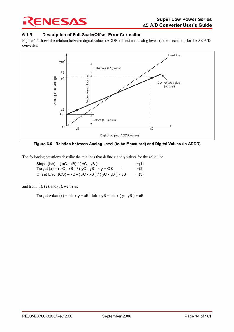
6.1.5 Description of Full-Scale/Offset Error Correction Figure 6.5 shows the relation between digital values (ADDR values) and analog levels (to be measured) for the ∆Σ A/D converter.
Digital output (ADDR value)
Analo
g input voltage
Vref
xC
yB yC
xB
FS
OS
O
Offset (OS) error
Me
asu
rem
en
t ra
ng
e
Full-scale (FS) error
Ideal line
Converted value
(actual)
Figure 6.5 Relation between Analog Level (to be Measured) and Digital Values (in ADDR)
The following equations describe the relations that define x and y values for the solid line.
Slope (lsb) = ( xC - xB) / ( yC - yB ) ···(1) Target (x) = ( xC - xB ) / ( yC - yB ) * y + OS · ··(2) Offset Error (OS) = xB - ( xC - xB ) / ( yC - yB ) * yB ···(3)
and from (1), (2), and (3), we have:
Target value (x) = lsb * y + xB - lsb * yB = lsb * ( y - yB ) + xB
Super Low Power Series ∆Σ A/D Converter User's Guide
REJ05B0780-0200/Rev.2.00 September 2006 Page 35 of 161
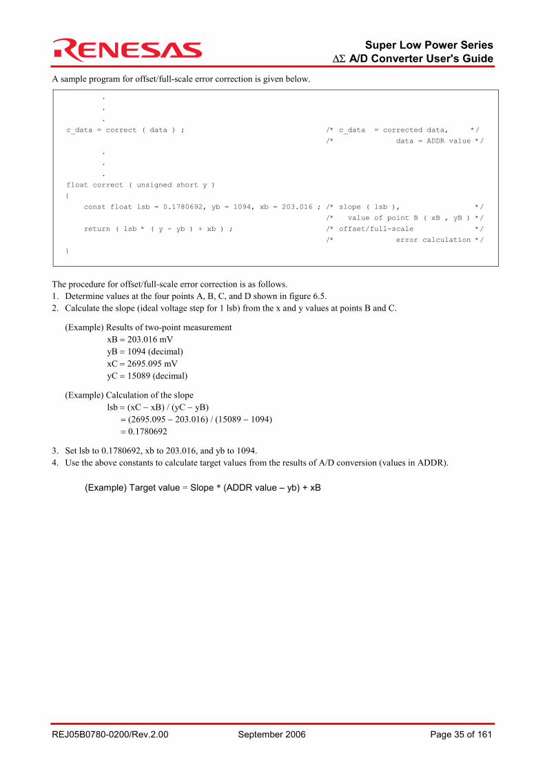
A sample program for offset/full-scale error correction is given below.
.
.
.
c_data = correct ( data ) ; /* c_data = corrected data, */
/* data = ADDR value */
.
.
.
float correct ( unsigned short y )
const float lsb = 0.1780692, yb = 1094, xb = 203.016 ; /* slope ( lsb ), */
/* value of point B ( xB , yB ) */
return ( lsb * ( y - yb ) + xb ) ; /* offset/full-scale */
/* error calculation */
The procedure for offset/full-scale error correction is as follows. 1. Determine values at the four points A, B, C, and D shown in figure 6.5. 2. Calculate the slope (ideal voltage step for 1 lsb) from the x and y values at points B and C.
(Example) Results of two-point measurement xB = 203.016 mV yB = 1094 (decimal) xC = 2695.095 mV yC = 15089 (decimal)
(Example) Calculation of the slope lsb = (xC − xB) / (yC − yB) = (2695.095 − 203.016) / (15089 − 1094) = 0.1780692
3. Set lsb to 0.1780692, xb to 203.016, and yb to 1094. 4. Use the above constants to calculate target values from the results of A/D conversion (values in ADDR).
(Example) Target value = Slope * (ADDR value – yb) + xB
Super Low Power Series ∆Σ A/D Converter User's Guide
REJ05B0780-0200/Rev.2.00 September 2006 Page 36 of 161
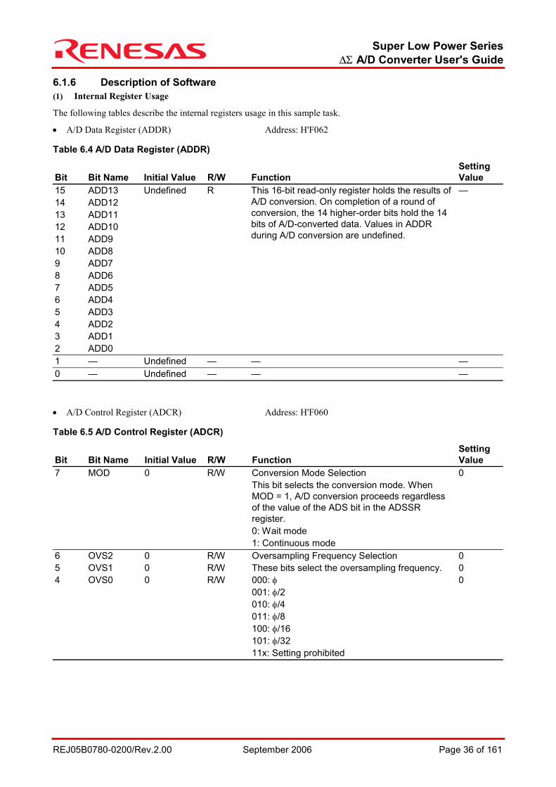
6.1.6 Description of Software (1) Internal Register Usage
The following tables describe the internal registers usage in this sample task.
• A/D Data Register (ADDR) Address: H'F062 Table 6.4 A/D Data Register (ADDR)
Bit Bit Name Initial Value R/W Function Setting Value
15 14 13 12 11 10 9 8 7 6 5 4 3 2
ADD13 ADD12 ADD11 ADD10 ADD9 ADD8 ADD7 ADD6 ADD5 ADD4 ADD3 ADD2 ADD1 ADD0
Undefined R This 16-bit read-only register holds the results of A/D conversion. On completion of a round of conversion, the 14 higher-order bits hold the 14 bits of A/D-converted data. Values in ADDR during A/D conversion are undefined.
—
1 — Undefined — — — 0 — Undefined — — — • A/D Control Register (ADCR) Address: H'F060 Table 6.5 A/D Control Register (ADCR)
Bit Bit Name Initial Value R/W Function Setting Value
7 MOD 0 R/W Conversion Mode Selection This bit selects the conversion mode. When MOD = 1, A/D conversion proceeds regardless of the value of the ADS bit in the ADSSR register. 0: Wait mode 1: Continuous mode
0
6 5 4
OVS2 OVS1 OVS0
0 0 0
R/W R/W R/W
Oversampling Frequency Selection These bits select the oversampling frequency. 000: φ 001: φ/2 010: φ/4 011: φ/8 100: φ/16 101: φ/32 11x: Setting prohibited
0 0 0
Super Low Power Series ∆Σ A/D Converter User's Guide
REJ05B0780-0200/Rev.2.00 September 2006 Page 37 of 161
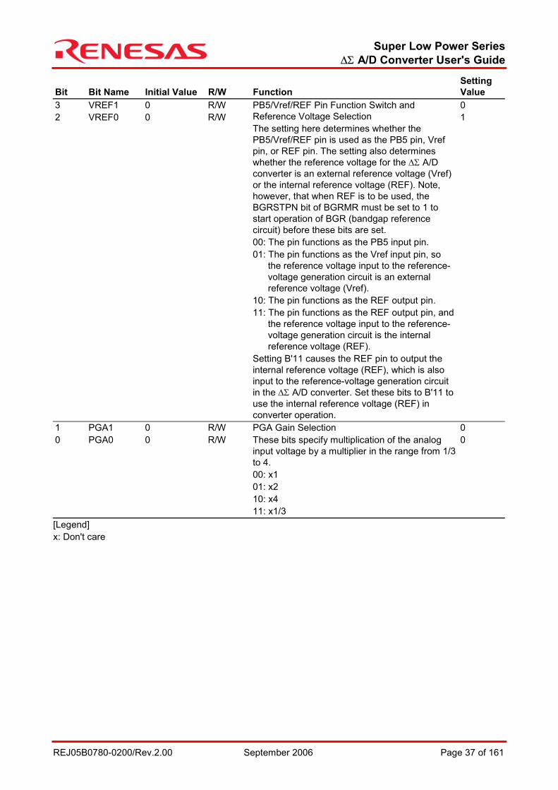
Bit Bit Name Initial Value R/W Function Setting Value
3 2
VREF1 VREF0
0 0
R/W R/W
PB5/Vref/REF Pin Function Switch and Reference Voltage Selection The setting here determines whether the PB5/Vref/REF pin is used as the PB5 pin, Vref pin, or REF pin. The setting also determines whether the reference voltage for the ∆Σ A/D converter is an external reference voltage (Vref) or the internal reference voltage (REF). Note, however, that when REF is to be used, the BGRSTPN bit of BGRMR must be set to 1 to start operation of BGR (bandgap reference circuit) before these bits are set. 00: The pin functions as the PB5 input pin. 01: The pin functions as the Vref input pin, so
the reference voltage input to the reference-voltage generation circuit is an external reference voltage (Vref).
10: The pin functions as the REF output pin. 11: The pin functions as the REF output pin, and
the reference voltage input to the reference-voltage generation circuit is the internal reference voltage (REF).
Setting B'11 causes the REF pin to output the internal reference voltage (REF), which is also input to the reference-voltage generation circuit in the ∆Σ A/D converter. Set these bits to B'11 to use the internal reference voltage (REF) in converter operation.
0 1
1 0
PGA1 PGA0
0 0
R/W R/W
PGA Gain Selection These bits specify multiplication of the analog input voltage by a multiplier in the range from 1/3 to 4. 00: x1 01: x2 10: x4 11: x1/3
0 0
[Legend] x: Don't care
Super Low Power Series ∆Σ A/D Converter User's Guide
REJ05B0780-0200/Rev.2.00 September 2006 Page 38 of 161
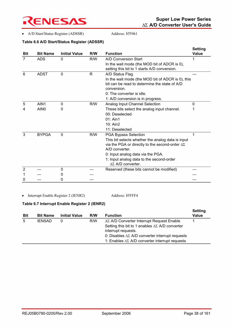
• A/D Start/Status Register (ADSSR) Address: H'F061 Table 6.6 A/D Start/Status Register (ADSSR)
Bit Bit Name Initial Value R/W Function Setting Value
7 ADS 0 R/W A/D Conversion Start In the wait mode (the MOD bit of ADCR is 0), setting this bit to 1 starts A/D conversion.
1
6 ADST 0 R A/D Status Flag In the wait mode (the MOD bit of ADCR is 0), this bit can be read to determine the state of A/D conversion. 0: The converter is idle. 1: A/D conversion is in progress.
—
5 4
AIN1 AIN0
0 0
R/W Analog Input Channel Selection These bits select the analog input channel. 00: Deselected 01: Ain1 10: Ain2 11: Deselected
0 1
3 BYPGA 0 R/W PGA Bypass Selection This bit selects whether the analog data is input via the PGA or directly to the second-order ∆Σ A/D converter. 0: Input analog data via the PGA. 1: Input analog data to the second-order
∆Σ A/D converter.
1
2 1 0
— — —
0 0 0
— — —
Reserved (these bits cannot be modified) — — —
• Interrupt Enable Register 2 (IENR2) Address: H'FFF4 Table 6.7 Interrupt Enable Register 2 (IENR2)
Bit Bit Name Initial Value R/W Function Setting Value
5 IENSAD 0 R/W ∆Σ A/D Converter Interrupt Request Enable Setting this bit to 1 enables ∆Σ A/D converter interrupt requests. 0: Disables ∆Σ A/D converter interrupt requests 1: Enables ∆Σ A/D converter interrupt requests
1
Super Low Power Series ∆Σ A/D Converter User's Guide
REJ05B0780-0200/Rev.2.00 September 2006 Page 39 of 161
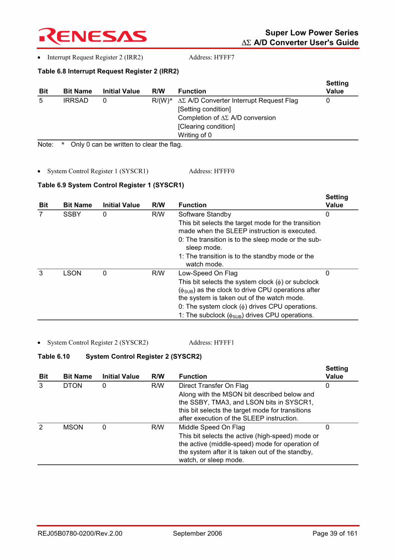
• Interrupt Request Register 2 (IRR2) Address: H'FFF7 Table 6.8 Interrupt Request Register 2 (IRR2)
Bit Bit Name Initial Value R/W Function Setting Value
5 IRRSAD 0 R/(W)* ∆Σ A/D Converter Interrupt Request Flag [Setting condition] Completion of ∆Σ A/D conversion [Clearing condition] Writing of 0
0
Note: * Only 0 can be written to clear the flag. • System Control Register 1 (SYSCR1) Address: H'FFF0 Table 6.9 System Control Register 1 (SYSCR1)
Bit Bit Name Initial Value R/W Function Setting Value
7 SSBY 0 R/W Software Standby This bit selects the target mode for the transition made when the SLEEP instruction is executed. 0: The transition is to the sleep mode or the sub-
sleep mode. 1: The transition is to the standby mode or the
watch mode.
0
3 LSON 0 R/W Low-Speed On Flag This bit selects the system clock (φ) or subclock (φSUB) as the clock to drive CPU operations after the system is taken out of the watch mode. 0: The system clock (φ) drives CPU operations. 1: The subclock (φSUB) drives CPU operations.
0
• System Control Register 2 (SYSCR2) Address: H'FFF1 Table 6.10 System Control Register 2 (SYSCR2)
Bit Bit Name Initial Value R/W Function Setting Value
3 DTON 0 R/W Direct Transfer On Flag Along with the MSON bit described below and the SSBY, TMA3, and LSON bits in SYSCR1, this bit selects the target mode for transitions after execution of the SLEEP instruction.
0
2 MSON 0 R/W Middle Speed On Flag This bit selects the active (high-speed) mode or the active (middle-speed) mode for operation of the system after it is taken out of the standby, watch, or sleep mode.
0
Super Low Power Series ∆Σ A/D Converter User's Guide
REJ05B0780-0200/Rev.2.00 September 2006 Page 40 of 161
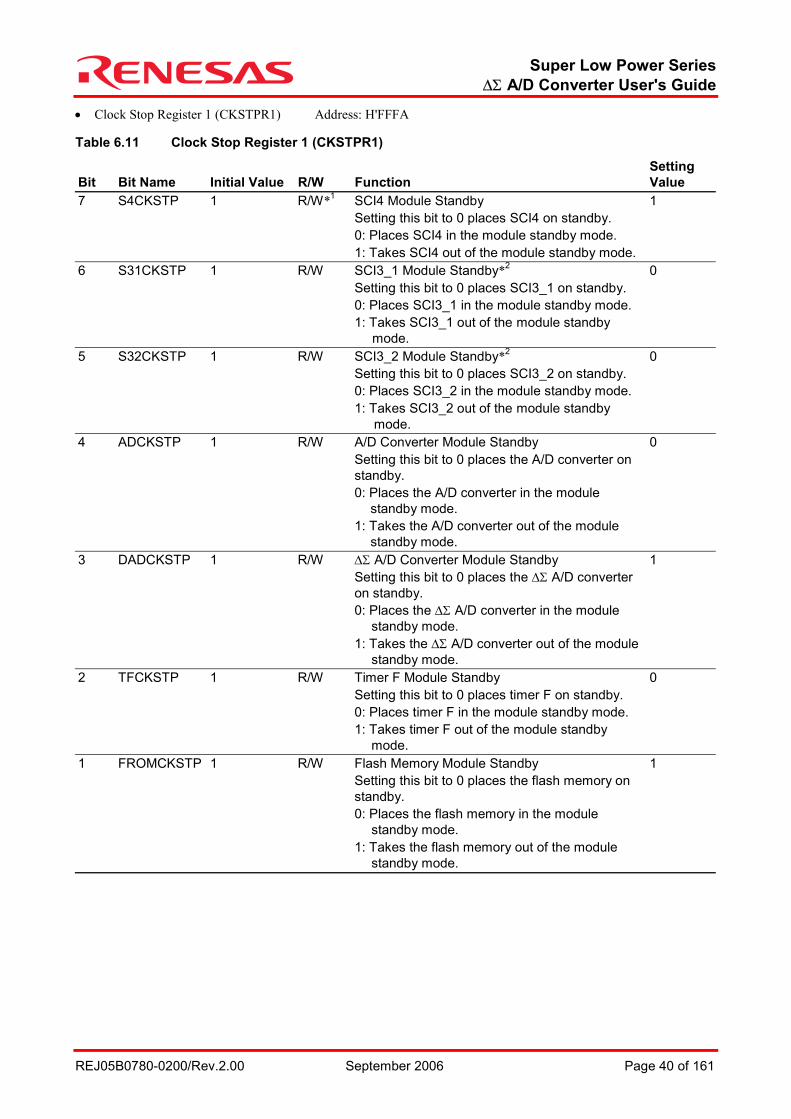
• Clock Stop Register 1 (CKSTPR1) Address: H'FFFA Table 6.11 Clock Stop Register 1 (CKSTPR1)
Bit Bit Name Initial Value R/W Function Setting Value
7 S4CKSTP 1 R/W*1 SCI4 Module Standby Setting this bit to 0 places SCI4 on standby. 0: Places SCI4 in the module standby mode. 1: Takes SCI4 out of the module standby mode.
1
6 S31CKSTP 1 R/W SCI3_1 Module Standby*2
Setting this bit to 0 places SCI3_1 on standby. 0: Places SCI3_1 in the module standby mode. 1: Takes SCI3_1 out of the module standby
mode.
0
5 S32CKSTP 1 R/W SCI3_2 Module Standby*2
Setting this bit to 0 places SCI3_2 on standby. 0: Places SCI3_2 in the module standby mode. 1: Takes SCI3_2 out of the module standby
mode.
0
4 ADCKSTP 1 R/W A/D Converter Module Standby Setting this bit to 0 places the A/D converter on standby. 0: Places the A/D converter in the module
standby mode. 1: Takes the A/D converter out of the module
standby mode.
0
3 DADCKSTP 1 R/W ∆Σ A/D Converter Module Standby Setting this bit to 0 places the ∆Σ A/D converter on standby. 0: Places the ∆Σ A/D converter in the module
standby mode. 1: Takes the ∆Σ A/D converter out of the module
standby mode.
1
2 TFCKSTP 1 R/W Timer F Module Standby Setting this bit to 0 places timer F on standby. 0: Places timer F in the module standby mode. 1: Takes timer F out of the module standby
mode.
0
1 FROMCKSTP 1 R/W Flash Memory Module Standby Setting this bit to 0 places the flash memory on standby. 0: Places the flash memory in the module
standby mode. 1: Takes the flash memory out of the module
standby mode.
1
Super Low Power Series ∆Σ A/D Converter User's Guide
REJ05B0780-0200/Rev.2.00 September 2006 Page 41 of 161
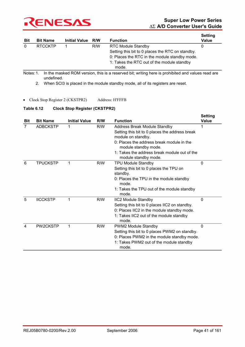
Bit Bit Name Initial Value R/W Function Setting Value
0 RTCCKTP 1 R/W RTC Module Standby Setting this bit to 0 places the RTC on standby. 0: Places the RTC in the module standby mode. 1: Takes the RTC out of the module standby
mode.
0
Notes: 1. In the masked ROM version, this is a reserved bit; writing here is prohibited and values read are undefined.
2. When SCI3 is placed in the module standby mode, all of its registers are reset. • Clock Stop Register 2 (CKSTPR2) Address: H'FFFB Table 6.12 Clock Stop Register (CKSTPR2)
Bit Bit Name Initial Value R/W Function Setting Value
7 ADBCKSTP 1 R/W Address Break Module Standby Setting this bit to 0 places the address break module on standby. 0: Places the address break module in the
module standby mode. 1: Takes the address break module out of the
module standby mode.
1
6 TPUCKSTP 1 R/W TPU Module Standby Setting this bit to 0 places the TPU on standby. 0: Places the TPU in the module standby
mode. 1: Takes the TPU out of the module standby
mode.
0
5 IICCKSTP 1 R/W IIC2 Module Standby Setting this bit to 0 places IIC2 on standby. 0: Places IIC2 in the module standby mode. 1: Takes IIC2 out of the module standby
mode.
0
4 PW2CKSTP 1 R/W PWM2 Module Standby Setting this bit to 0 places PWM2 on standby. 0: Places PWM2 in the module standby mode. 1: Takes PWM2 out of the module standby
mode.
0
Super Low Power Series ∆Σ A/D Converter User's Guide
REJ05B0780-0200/Rev.2.00 September 2006 Page 42 of 161
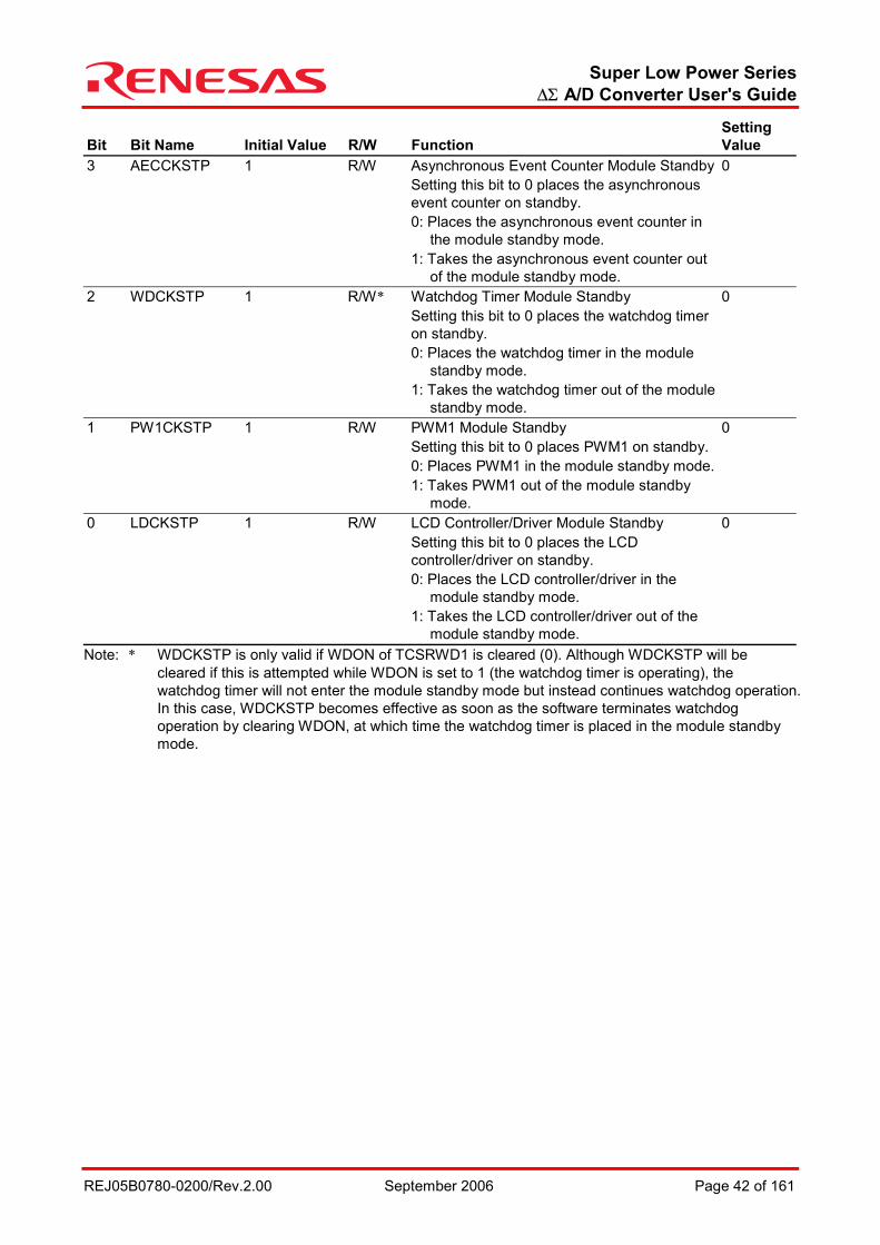
Bit Bit Name Initial Value R/W Function Setting Value
3 AECCKSTP 1 R/W Asynchronous Event Counter Module Standby Setting this bit to 0 places the asynchronous event counter on standby. 0: Places the asynchronous event counter in
the module standby mode. 1: Takes the asynchronous event counter out
of the module standby mode.
0
2 WDCKSTP 1 R/W* Watchdog Timer Module Standby Setting this bit to 0 places the watchdog timer on standby. 0: Places the watchdog timer in the module
standby mode. 1: Takes the watchdog timer out of the module
standby mode.
0
1 PW1CKSTP 1 R/W PWM1 Module Standby Setting this bit to 0 places PWM1 on standby. 0: Places PWM1 in the module standby mode. 1: Takes PWM1 out of the module standby
mode.
0
0 LDCKSTP 1 R/W LCD Controller/Driver Module Standby Setting this bit to 0 places the LCD controller/driver on standby. 0: Places the LCD controller/driver in the
module standby mode. 1: Takes the LCD controller/driver out of the
module standby mode.
0
Note: * WDCKSTP is only valid if WDON of TCSRWD1 is cleared (0). Although WDCKSTP will be cleared if this is attempted while WDON is set to 1 (the watchdog timer is operating), the watchdog timer will not enter the module standby mode but instead continues watchdog operation. In this case, WDCKSTP becomes effective as soon as the software terminates watchdog operation by clearing WDON, at which time the watchdog timer is placed in the module standby mode.
Super Low Power Series ∆Σ A/D Converter User's Guide
REJ05B0780-0200/Rev.2.00 September 2006 Page 43 of 161
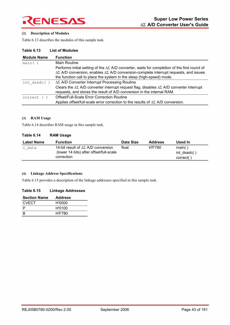
(2) Description of Modules
Table 6.13 describes the modules of this sample task. Table 6.13 List of Modules
Module Name Function main( ) Main Routine
Performs initial setting of the ∆Σ A/D converter, waits for completion of the first round of ∆Σ A/D conversion, enables ∆Σ A/D conversion-complete interrupt requests, and issues the function call to place the system in the sleep (high-speed) mode.
int_dsadc( ) ∆Σ A/D Converter Interrupt Processing Routine Clears the ∆Σ A/D converter interrupt request flag, disables ∆Σ A/D converter interrupt requests, and stores the result of A/D conversion in the internal RAM.
correct ( ) Offset/Full-Scale Error Correction Routine Applies offset/full-scale error correction to the results of ∆Σ A/D conversion.
(3) RAM Usage
Table 6.14 describes RAM usage in this sample task. Table 6.14 RAM Usage
Label Name Function Data Size Address Used In c_data 14-bit result of ∆Σ A/D conversion
(lower 14 bits) after offset/full-scale correction
float H'F780 main( ) int_dsadc( ) correct( )
(4) Linkage Address Specifications
Table 6.15 provides a description of the linkage addresses specified in this sample task. Table 6.15 Linkage Addresses
Section Name Address CVECT H'0000 P H'0100 B H'F780
Super Low Power Series ∆Σ A/D Converter User's Guide
REJ05B0780-0200/Rev.2.00 September 2006 Page 44 of 161
6.1.7 Flowcharts (1) Main Routine
main()
SP = H'FF80 Issue a #pragma entry main (SP = 0xFF80) directive to set the stack pointer to H'FF80 .
CCR I-bit = 1 Set the I bit of the CCR to 1 to disable interrupts.
ad_data = H'0000 Initialize the RAM area to be used.
ADS = 0 Clear the ADS bit to 0 by software.
ADS = 1 Start the second round of A/D conversion.
ADS = 1 Start the first round of A/D conversion.
ADST = 0?No
Yes
Wait for the first round to end.
IRRSAD = 0
Enable ∆Σ A/D converter interrupt requests.
IENSAD = 1
CCR I-bit = 0 Set the I bit of the CCR to 0 to enable interrupts.
sleep() Make the transition to the sleep (high-speed) mode.
Note: * In this sample task, all internal peripheral modules other than SCI4, the flash memory module, address break, and ∆Σ A/D converter are placed in the module standby mode. The user should write 1 to the corresponding bits in the clock stop registers to take other required peripheral modules out of the module standby mode.
CKSTPR1 = H'8ASet CKSTPR1 to place SCI3_1, SCI3_2, the A/D converter, timer F, the RTC, the TPU, and IIC2 and CKSTPR2 to place PWM1, PWM2, the asynchronous event counter, the watchdog timer, and the LCDC in the module standby mode.*
CKSTPR2 = H'80
ADCR = H'04Make initial settings for the ∆Σ A/D converter (wait mode, oversampling frequency (φ), PB5/Vref/REF terminal functioning as the Vref input pin, reference voltage (external reference voltage), analog input (Ain1), and PGA bypass mode).
ADSSR = H'18
SYSCR1 = H'03
Make initial settings of the system control registers, selecting transition to the sleep (high-speed) mode (LSON = 0, MSON = 0, SSBY = 0, DTON = 0).
SYSCR2 = H'E0
Figure 6.6 Main Routine Flowchart
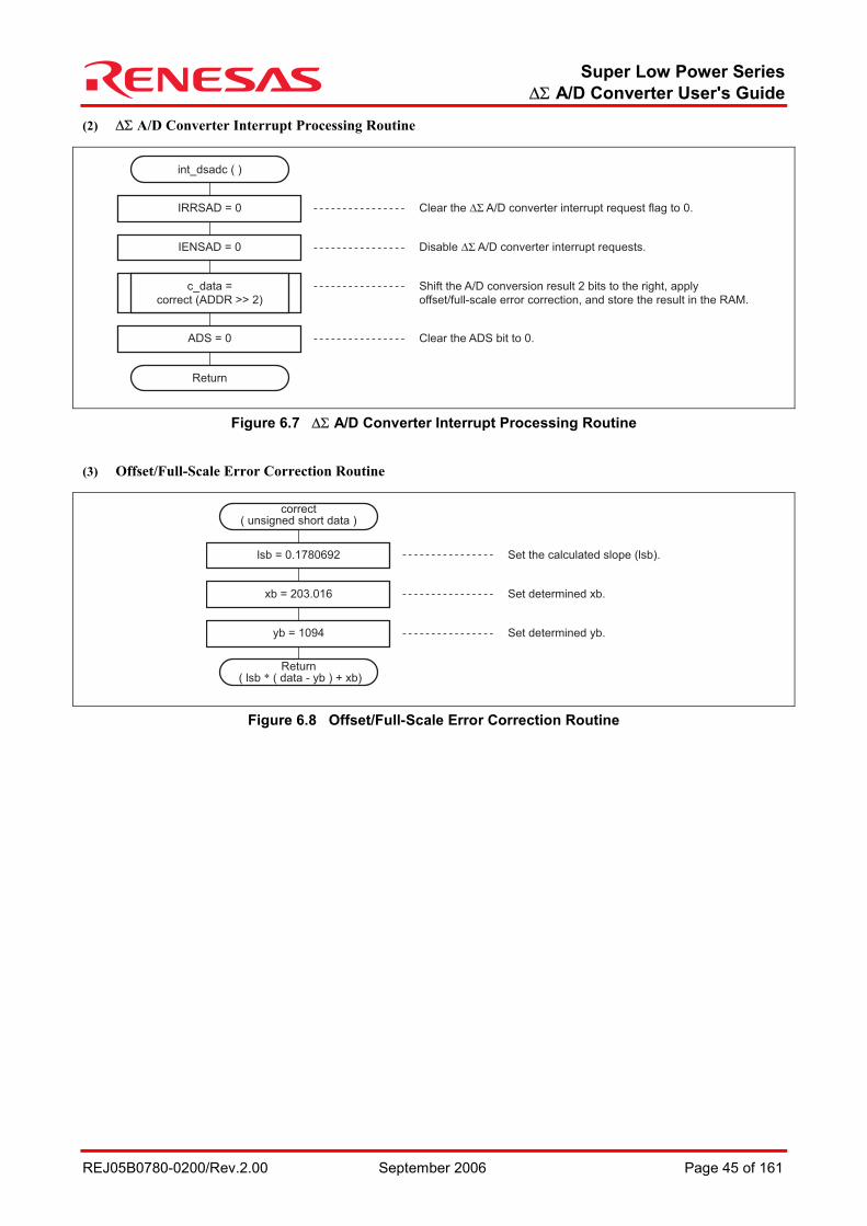
Super Low Power Series ∆Σ A/D Converter User's Guide
REJ05B0780-0200/Rev.2.00 September 2006 Page 45 of 161
(2) ∆Σ A/D Converter Interrupt Processing Routine
int_dsadc ( )
Return
IRRSAD = 0 Clear the ∆Σ A/D converter interrupt request flag to 0.
IENSAD = 0 Disable ∆Σ A/D converter interrupt requests.
c_data =
correct (ADDR >> 2)
Shift the A/D conversion result 2 bits to the right, apply
offset/full-scale error correction, and store the result in the RAM.
ADS = 0 Clear the ADS bit to 0.
Figure 6.7 ∆Σ A/D Converter Interrupt Processing Routine
(3) Offset/Full-Scale Error Correction Routine
correct( unsigned short data )
Return ( lsb * ( data - yb ) + xb)
lsb = 0.1780692 Set the calculated slope (lsb).
xb = 203.016 Set determined xb.
yb = 1094 Set determined yb.
Figure 6.8 Offset/Full-Scale Error Correction Routine
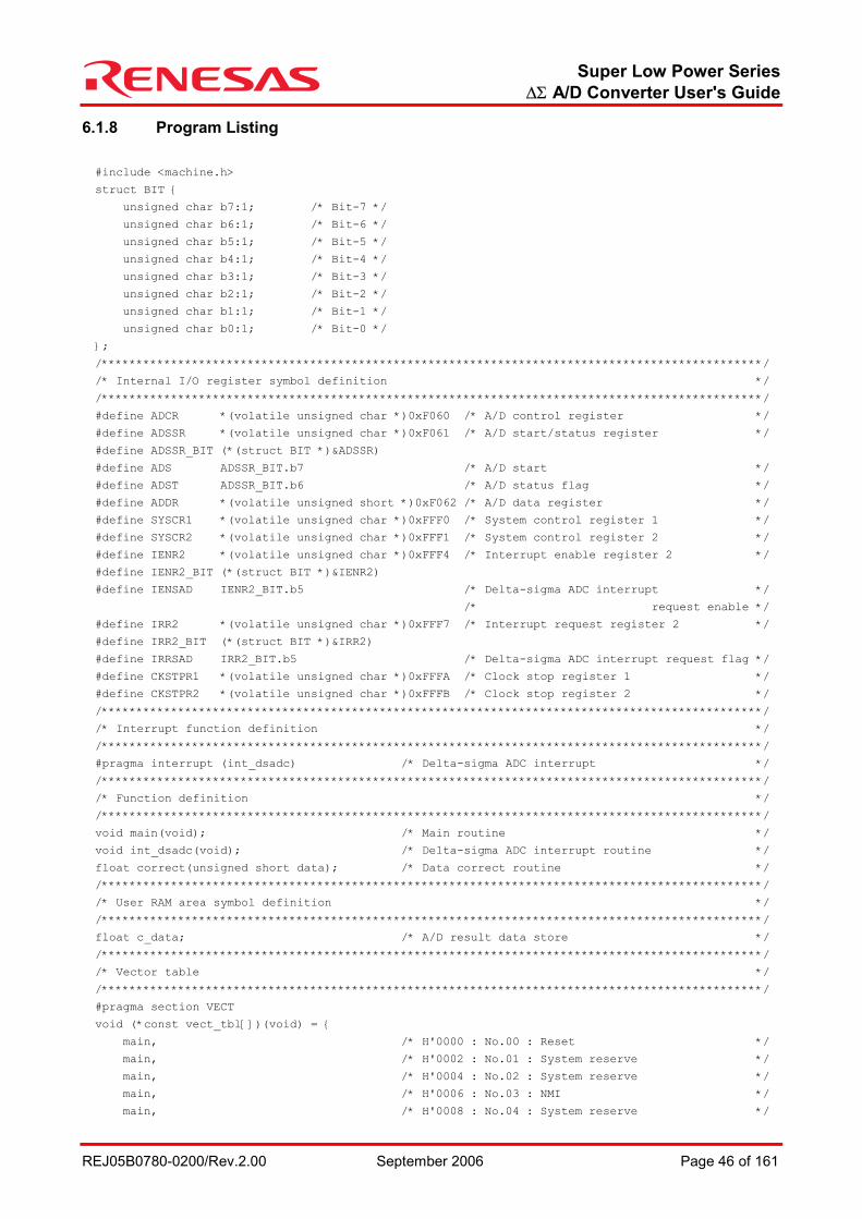
Super Low Power Series ∆Σ A/D Converter User's Guide
REJ05B0780-0200/Rev.2.00 September 2006 Page 46 of 161
6.1.8 Program Listing #include <machine.h>
struct BIT
unsigned char b7:1; /* Bit-7 */
unsigned char b6:1; /* Bit-6 */
unsigned char b5:1; /* Bit-5 */
unsigned char b4:1; /* Bit-4 */
unsigned char b3:1; /* Bit-3 */
unsigned char b2:1; /* Bit-2 */
unsigned char b1:1; /* Bit-1 */
unsigned char b0:1; /* Bit-0 */
;
/***********************************************************************************************/
/* Internal I/O register symbol definition */
/***********************************************************************************************/
#define ADCR *(volatile unsigned char *)0xF060 /* A/D control register */
#define ADSSR *(volatile unsigned char *)0xF061 /* A/D start/status register */
#define ADSSR_BIT (*(struct BIT *)&ADSSR)
#define ADS ADSSR_BIT.b7 /* A/D start */
#define ADST ADSSR_BIT.b6 /* A/D status flag */
#define ADDR *(volatile unsigned short *)0xF062 /* A/D data register */
#define SYSCR1 *(volatile unsigned char *)0xFFF0 /* System control register 1 */
#define SYSCR2 *(volatile unsigned char *)0xFFF1 /* System control register 2 */
#define IENR2 *(volatile unsigned char *)0xFFF4 /* Interrupt enable register 2 */
#define IENR2_BIT (*(struct BIT *)&IENR2)
#define IENSAD IENR2_BIT.b5 /* Delta-sigma ADC interrupt */
/* request enable */
#define IRR2 *(volatile unsigned char *)0xFFF7 /* Interrupt request register 2 */
#define IRR2_BIT (*(struct BIT *)&IRR2)
#define IRRSAD IRR2_BIT.b5 /* Delta-sigma ADC interrupt request flag */
#define CKSTPR1 *(volatile unsigned char *)0xFFFA /* Clock stop register 1 */
#define CKSTPR2 *(volatile unsigned char *)0xFFFB /* Clock stop register 2 */
/***********************************************************************************************/
/* Interrupt function definition */
/***********************************************************************************************/
#pragma interrupt (int_dsadc) /* Delta-sigma ADC interrupt */
/***********************************************************************************************/
/* Function definition */
/***********************************************************************************************/
void main(void); /* Main routine */
void int_dsadc(void); /* Delta-sigma ADC interrupt routine */
float correct(unsigned short data); /* Data correct routine */
/***********************************************************************************************/
/* User RAM area symbol definition */
/***********************************************************************************************/
float c_data; /* A/D result data store */
/***********************************************************************************************/
/* Vector table */
/***********************************************************************************************/
#pragma section VECT
void (*const vect_tbl[])(void) =
main, /* H'0000 : No.00 : Reset */
main, /* H'0002 : No.01 : System reserve */
main, /* H'0004 : No.02 : System reserve */
main, /* H'0006 : No.03 : NMI */
main, /* H'0008 : No.04 : System reserve */
Super Low Power Series ∆Σ A/D Converter User's Guide
REJ05B0780-0200/Rev.2.00 September 2006 Page 47 of 161
main, /* H'000A : No.05 : Address break */
main, /* H'000C : No.06 : IRQ0 */
main, /* H'000E : No.07 : IRQ1 */
main, /* H'0010 : No.08 : IRQAEC */
main, /* H'0012 : No.09 : IRQ3 */
main, /* H'0014 : No.10 : IRQ4 */
main, /* H'0016 : No.11 : WKP0 */
main, /* H'0018 : No.12 : WKP1 */
main, /* H'001A : No.13 : WKP2 */
main, /* H'001C : No.14 : WKP3 */
main, /* H'001E : No.15 : WKP4 */
main, /* H'0020 : No.16 : WKP5 */
main, /* H'0022 : No.17 : WKP6 */
main, /* H'0024 : No.18 : WKP7 */
main, /* H'0026 : No.19 : RTC - 0.25sec overflow */
main, /* H'0028 : No.20 : RTC - 0.5sec overflow */
main, /* H'002A : No.21 : RTC - second periodic overflow */
main, /* H'002C : No.22 : RTC - minute periodic overflow */
main, /* H'002E : No.23 : RTC - hour periodic overflow */
main, /* H'0030 : No.24 : RTC - day periodic overflow */
main, /* H'0032 : No.25 : RTC - week periodic overflow */
main, /* H'0034 : No.26 : RTC - free-run overflow */
main, /* H'0036 : No.27 : WDT */
main, /* H'0038 : No.28 : AEC */
main, /* H'003A : No.29 : TPU_1 - TG1A */
main, /* H'003C : No.30 : TPU_1 - TG1B */
main, /* H'003E : No.31 : TPU_1 - TCI1V */
main, /* H'0040 : No.32 : TPU_2 - TG2A */
main, /* H'0042 : No.33 : TPU_2 - TG2B */
main, /* H'0044 : No.34 : TPU_2 - TCI2V */
main, /* H'0046 : No.35 : Timer FL */
main, /* H'0048 : No.36 : Timer FH */
main, /* H'004A : No.37 : SCI4 */
main, /* H'004C : No.38 : SCI3_1 */
main, /* H'004E : No.39 : SCI3_2 */
main, /* H'0050 : No.40 : IIC2 */
int_dsadc, /* H'0052 : No.41 : Delta-sigma ADC */
main, /* H'0054 : No.42 : 10-bit ADC */
main /* H'0056 : No.43 : Direct transition */
;
#pragma entry main(sp = 0xFF80) /* SP = H'FF80 */
#pragma section
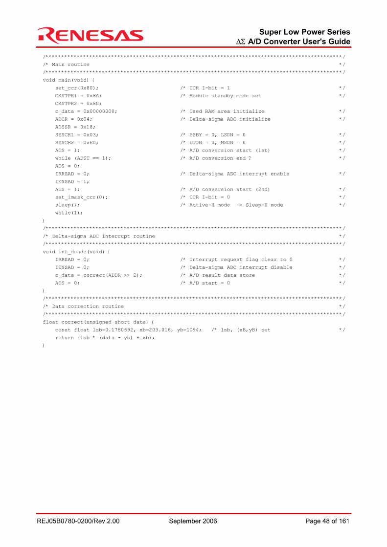
Super Low Power Series ∆Σ A/D Converter User's Guide
REJ05B0780-0200/Rev.2.00 September 2006 Page 48 of 161
/***********************************************************************************************/
/* Main routine */
/***********************************************************************************************/
void main(void)
set_ccr(0x80); /* CCR I-bit = 1 */
CKSTPR1 = 0x8A; /* Module standby mode set */
CKSTPR2 = 0x80;
c_data = 0x00000000; /* Used RAM area initialize */
ADCR = 0x04; /* Delta-sigma ADC initialize */
ADSSR = 0x18;
SYSCR1 = 0x03; /* SSBY = 0, LSON = 0 */
SYSCR2 = 0xE0; /* DTON = 0, MSON = 0 */
ADS = 1; /* A/D conversion start (1st) */
while (ADST == 1); /* A/D conversion end ? */
ADS = 0;
IRRSAD = 0; /* Delta-sigma ADC interrupt enable */
IENSAD = 1;
ADS = 1; /* A/D conversion start (2nd) */
set_imask_ccr(0); /* CCR I-bit = 0 */
sleep(); /* Active-H mode -> Sleep-H mode */
while(1);
/***********************************************************************************************/
/* Delta-sigma ADC interrupt routine */
/***********************************************************************************************/
void int_dsadc(void)
IRRSAD = 0; /* Interrupt request flag clear to 0 */
IENSAD = 0; /* Delta-sigma ADC interrupt disable */
c_data = correct(ADDR >> 2); /* A/D result data store */
ADS = 0; /* A/D start = 0 */
/***********************************************************************************************/
/* Data correction routine */
/***********************************************************************************************/
float correct(unsigned short data)
const float lsb=0.1780692, xb=203.016, yb=1094; /* lsb, (xB,yB) set */
return (lsb * (data - yb) + xb);
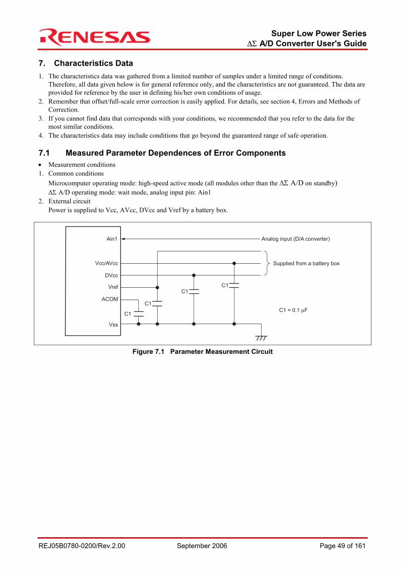
Super Low Power Series ∆Σ A/D Converter User's Guide
REJ05B0780-0200/Rev.2.00 September 2006 Page 49 of 161
7. Characteristics Data 1. The characteristics data was gathered from a limited number of samples under a limited range of conditions.
Therefore, all data given below is for general reference only, and the characteristics are not guaranteed. The data are provided for reference by the user in defining his/her own conditions of usage.
2. Remember that offset/full-scale error correction is easily applied. For details, see section 4, Errors and Methods of Correction.
3. If you cannot find data that corresponds with your conditions, we recommended that you refer to the data for the most similar conditions.
4. The characteristics data may include conditions that go beyond the guaranteed range of safe operation.
7.1 Measured Parameter Dependences of Error Components • Measurement conditions 1. Common conditions
Microcomputer operating mode: high-speed active mode (all modules other than the ∆Σ A/D on standby) ∆Σ A/D operating mode: wait mode, analog input pin: Ain1
2. External circuit Power is supplied to Vcc, AVcc, DVcc and Vref by a battery box.
Ain1
Vcc/AVcc
C1
C1
Vss
C1 = 0.1 µF
Analog input (D/A converter)
Supplied from a battery box
C1C1
DVcc
Vref
ACOM
Figure 7.1 Parameter Measurement Circuit
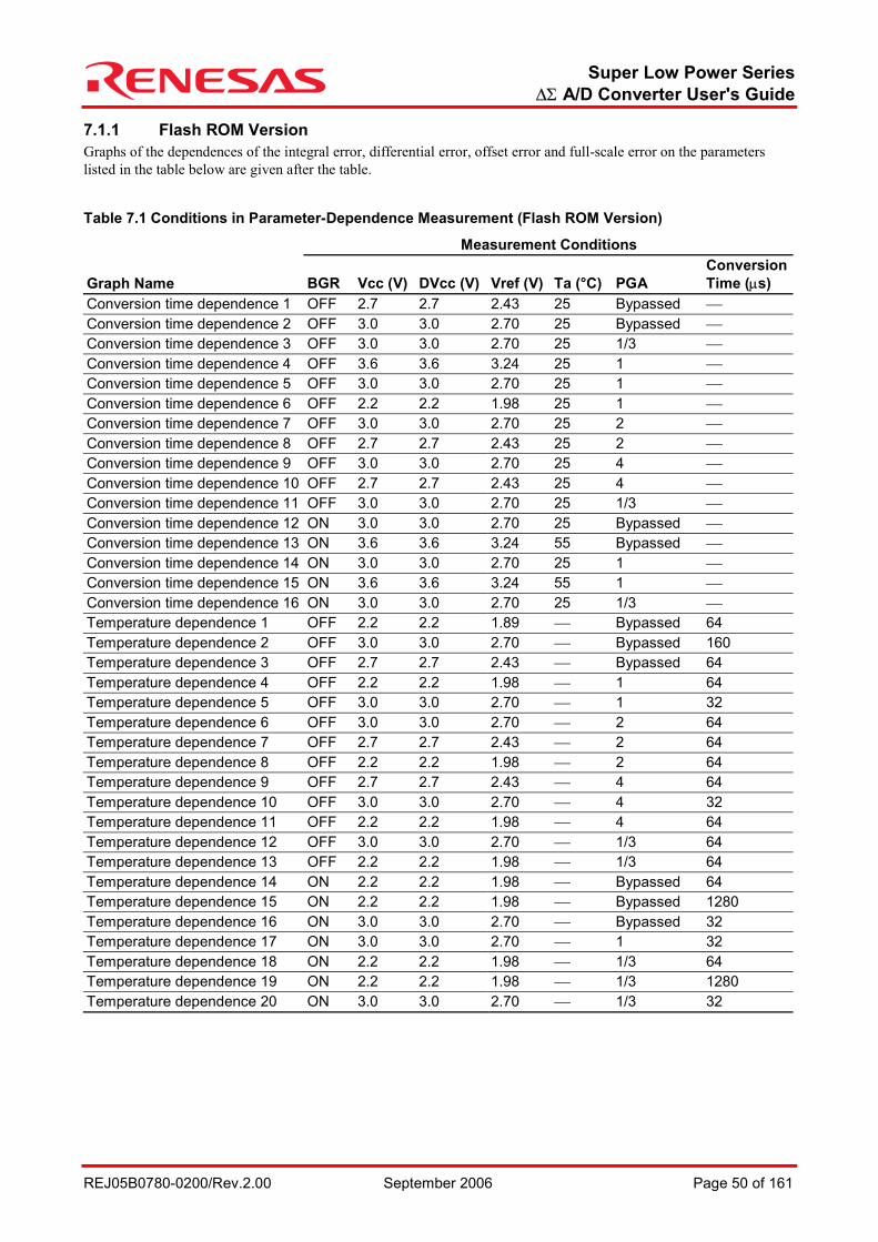
Super Low Power Series ∆Σ A/D Converter User's Guide
REJ05B0780-0200/Rev.2.00 September 2006 Page 50 of 161
7.1.1 Flash ROM Version Graphs of the dependences of the integral error, differential error, offset error and full-scale error on the parameters listed in the table below are given after the table.
Table 7.1 Conditions in Parameter-Dependence Measurement (Flash ROM Version)
Measurement Conditions
Graph Name BGR Vcc (V) DVcc (V) Vref (V) Ta (°C) PGA Conversion Time (µs)
Conversion time dependence 1 OFF 2.7 2.7 2.43 25 Bypassed Conversion time dependence 2 OFF 3.0 3.0 2.70 25 Bypassed Conversion time dependence 3 OFF 3.0 3.0 2.70 25 1/3 Conversion time dependence 4 OFF 3.6 3.6 3.24 25 1 Conversion time dependence 5 OFF 3.0 3.0 2.70 25 1 Conversion time dependence 6 OFF 2.2 2.2 1.98 25 1 Conversion time dependence 7 OFF 3.0 3.0 2.70 25 2 Conversion time dependence 8 OFF 2.7 2.7 2.43 25 2 Conversion time dependence 9 OFF 3.0 3.0 2.70 25 4 Conversion time dependence 10 OFF 2.7 2.7 2.43 25 4 Conversion time dependence 11 OFF 3.0 3.0 2.70 25 1/3 Conversion time dependence 12 ON 3.0 3.0 2.70 25 Bypassed Conversion time dependence 13 ON 3.6 3.6 3.24 55 Bypassed Conversion time dependence 14 ON 3.0 3.0 2.70 25 1 Conversion time dependence 15 ON 3.6 3.6 3.24 55 1 Conversion time dependence 16 ON 3.0 3.0 2.70 25 1/3 Temperature dependence 1 OFF 2.2 2.2 1.89 Bypassed 64 Temperature dependence 2 OFF 3.0 3.0 2.70 Bypassed 160 Temperature dependence 3 OFF 2.7 2.7 2.43 Bypassed 64 Temperature dependence 4 OFF 2.2 2.2 1.98 1 64 Temperature dependence 5 OFF 3.0 3.0 2.70 1 32 Temperature dependence 6 OFF 3.0 3.0 2.70 2 64 Temperature dependence 7 OFF 2.7 2.7 2.43 2 64 Temperature dependence 8 OFF 2.2 2.2 1.98 2 64 Temperature dependence 9 OFF 2.7 2.7 2.43 4 64 Temperature dependence 10 OFF 3.0 3.0 2.70 4 32 Temperature dependence 11 OFF 2.2 2.2 1.98 4 64 Temperature dependence 12 OFF 3.0 3.0 2.70 1/3 64 Temperature dependence 13 OFF 2.2 2.2 1.98 1/3 64 Temperature dependence 14 ON 2.2 2.2 1.98 Bypassed 64 Temperature dependence 15 ON 2.2 2.2 1.98 Bypassed 1280 Temperature dependence 16 ON 3.0 3.0 2.70 Bypassed 32 Temperature dependence 17 ON 3.0 3.0 2.70 1 32 Temperature dependence 18 ON 2.2 2.2 1.98 1/3 64 Temperature dependence 19 ON 2.2 2.2 1.98 1/3 1280 Temperature dependence 20 ON 3.0 3.0 2.70 1/3 32
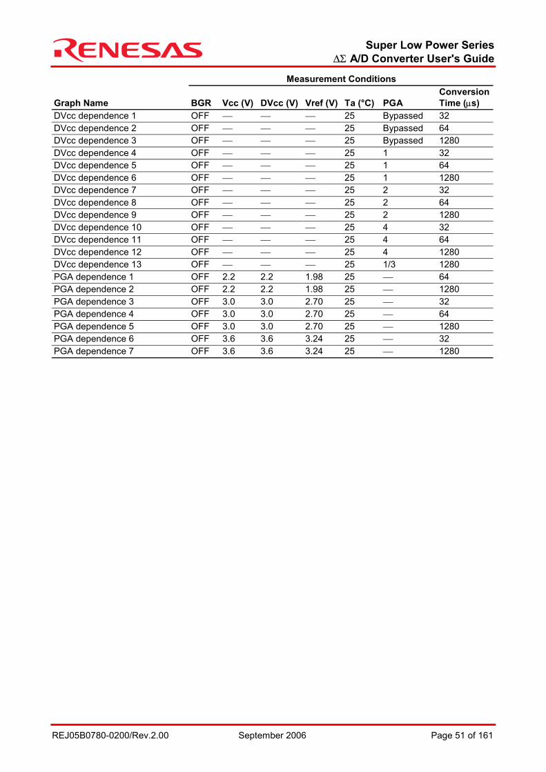
Super Low Power Series ∆Σ A/D Converter User's Guide
REJ05B0780-0200/Rev.2.00 September 2006 Page 51 of 161
Measurement Conditions
Graph Name BGR Vcc (V) DVcc (V) Vref (V) Ta (°C) PGA Conversion Time (µs)
DVcc dependence 1 OFF 25 Bypassed 32 DVcc dependence 2 OFF 25 Bypassed 64 DVcc dependence 3 OFF 25 Bypassed 1280 DVcc dependence 4 OFF 25 1 32 DVcc dependence 5 OFF 25 1 64 DVcc dependence 6 OFF 25 1 1280 DVcc dependence 7 OFF 25 2 32 DVcc dependence 8 OFF 25 2 64 DVcc dependence 9 OFF 25 2 1280 DVcc dependence 10 OFF 25 4 32 DVcc dependence 11 OFF 25 4 64 DVcc dependence 12 OFF 25 4 1280 DVcc dependence 13 OFF 25 1/3 1280 PGA dependence 1 OFF 2.2 2.2 1.98 25 64 PGA dependence 2 OFF 2.2 2.2 1.98 25 1280 PGA dependence 3 OFF 3.0 3.0 2.70 25 32 PGA dependence 4 OFF 3.0 3.0 2.70 25 64 PGA dependence 5 OFF 3.0 3.0 2.70 25 1280 PGA dependence 6 OFF 3.6 3.6 3.24 25 32 PGA dependence 7 OFF 3.6 3.6 3.24 25 1280
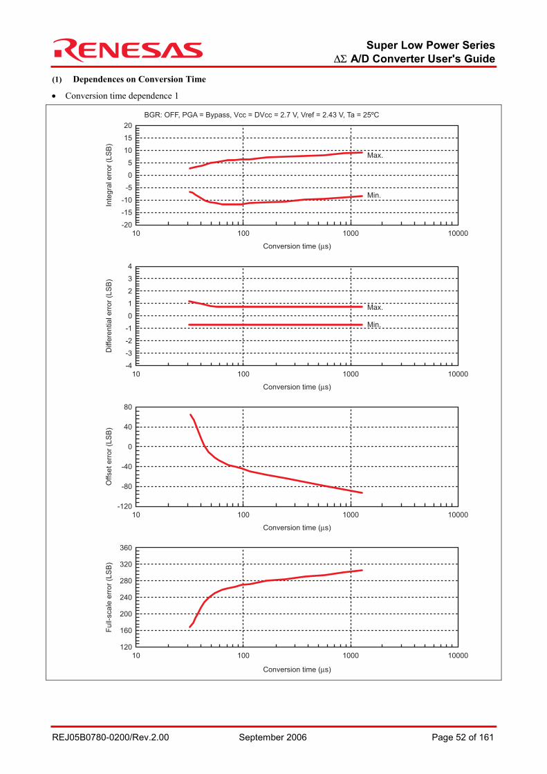
Super Low Power Series ∆Σ A/D Converter User's Guide
REJ05B0780-0200/Rev.2.00 September 2006 Page 52 of 161
(1) Dependences on Conversion Time
• Conversion time dependence 1 In
tegra
l err
or
(LS
B)
Conversion time (µs)
10010-20
-15
-10
-5
0
5
10
15
20
1000 10000
BGR: OFF, PGA = Bypass, Vcc = DVcc = 2.7 V, Vref = 2.43 V, Ta = 25ºCD
iffe
ren
tia
l e
rro
r (L
SB
)
Conversion time (µs)
10010-4
-3
-2
-1
0
1
2
3
4
1000 10000
Offset err
or
(LS
B)
Conversion time (µs)
10010-120
-80
-40
0
40
80
1000 10000
Fu
ll-sca
le e
rro
r (L
SB
)
Conversion time (µs)
10010120
160
200
240
280
320
360
1000 10000
Max.
Min.
Max.
Min.
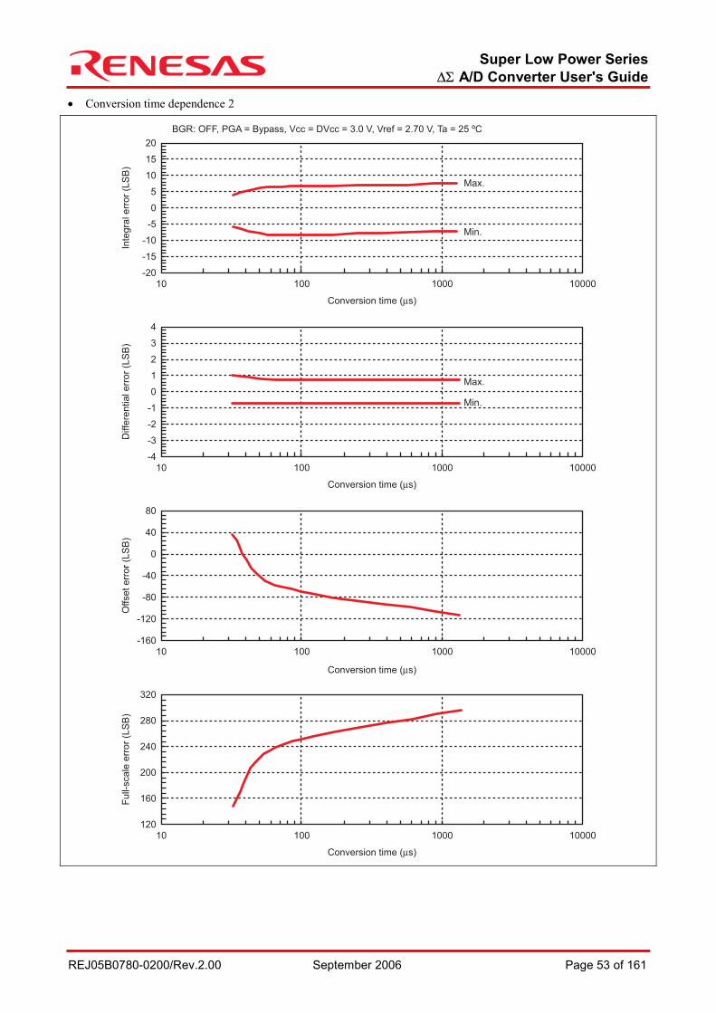
Super Low Power Series ∆Σ A/D Converter User's Guide
REJ05B0780-0200/Rev.2.00 September 2006 Page 53 of 161
• Conversion time dependence 2
Inte
gra
l err
or
(LS
B)
Conversion time (µs)
10010-20
-15
-10
-5
0
5
10
15
20
1000 10000
BGR: OFF, PGA = Bypass, Vcc = DVcc = 3.0 V, Vref = 2.70 V, Ta = 25 ºCD
iffe
rential err
or
(LS
B)
Conversion time (µs)
10010-4
-3
-2
-1
0
1
2
3
4
1000 10000
Full-
scale
err
or
(LS
B)
Conversion time (µs)
10010120
160
200
240
280
320
1000 10000
Offset err
or
(LS
B)
Conversion time (µs)
10010-160
-120
-80
-40
0
40
80
1000 10000
Max.
Min.
Max.
Min.
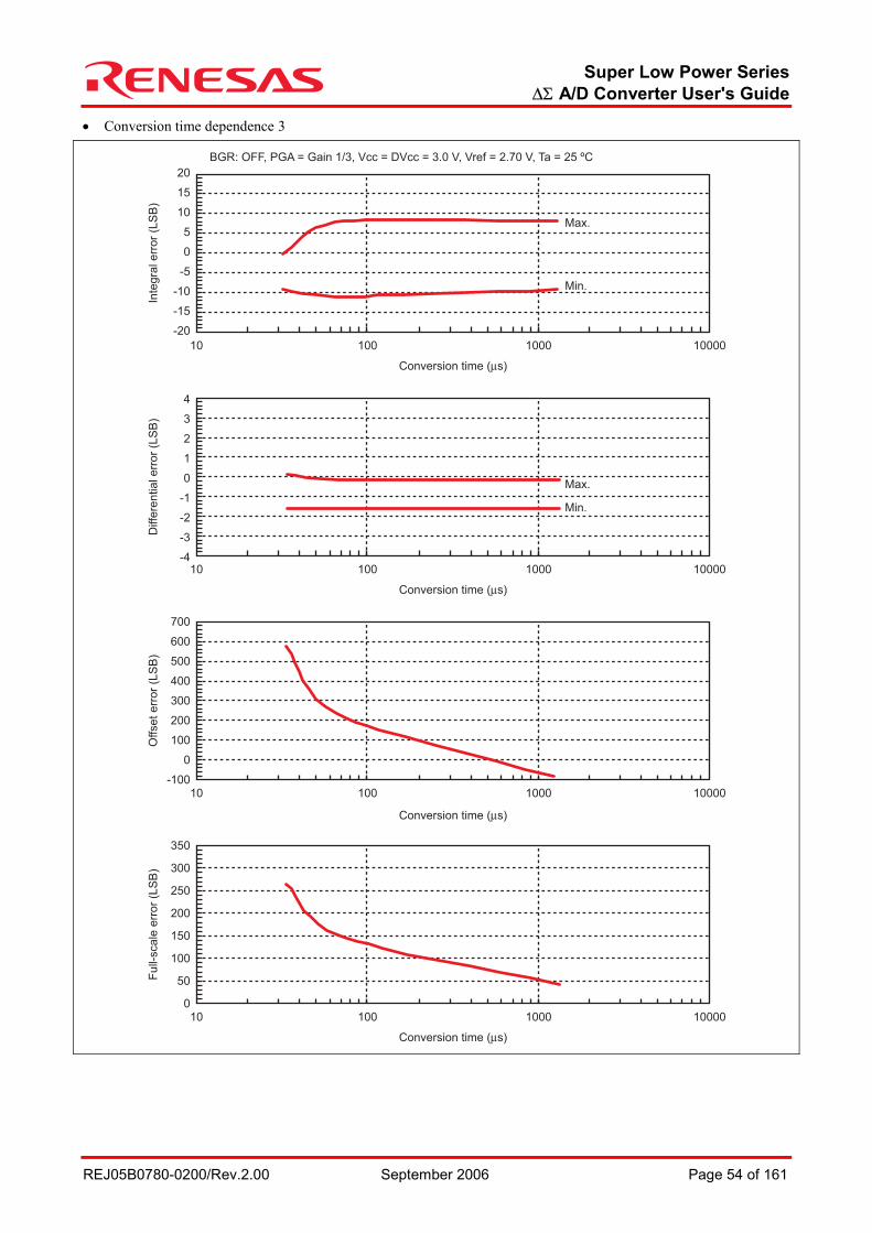
Super Low Power Series ∆Σ A/D Converter User's Guide
REJ05B0780-0200/Rev.2.00 September 2006 Page 54 of 161
• Conversion time dependence 3
Inte
gra
l err
or
(LS
B)
Conversion time (µs)
10010
-20
-15
-10
-5
0
5
10
15
20
1000 10000
BGR: OFF, PGA = Gain 1/3, Vcc = DVcc = 3.0 V, Vref = 2.70 V, Ta = 25 ºCD
iffe
rential err
or
(LS
B)
Conversion time (µs)
10010-4
-3
-2
-1
0
1
2
3
4
1000 10000
Full-
scale
err
or
(LS
B)
Conversion time (µs)
0
150
100
50
200
250
350
300
Offset err
or
(LS
B)
Conversion time (µs)
0
-100
100
200
300
400
500
600
700
10010 1000 10000
10010 1000 10000
Max.
Min.
Max.
Min.
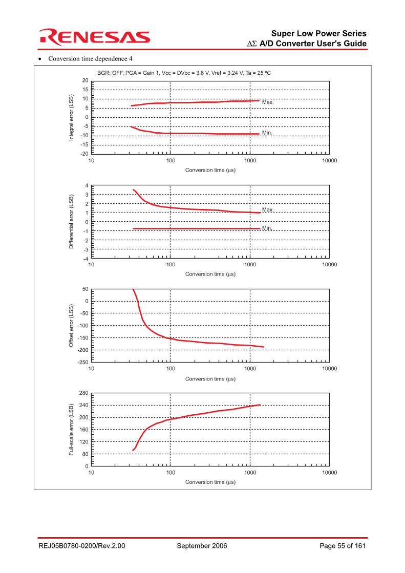
Super Low Power Series ∆Σ A/D Converter User's Guide
REJ05B0780-0200/Rev.2.00 September 2006 Page 55 of 161
• Conversion time dependence 4
Inte
gra
l err
or
(LS
B)
Conversion time (µs)
10010
-20
-15
-10
-5
0
5
10
15
20
1000 10000
BGR: OFF, PGA = Gain 1, Vcc = DVcc = 3.6 V, Vref = 3.24 V, Ta = 25 ºCD
iffe
rential err
or
(LS
B)
Conversion time (µs)
10010-4
-3
-2
-1
0
1
2
3
4
1000 10000
Full-
scale
err
or
(LS
B)
Conversion time (µs)
0
160
120
80
200
240
280
Offset err
or
(LS
B)
Conversion time (µs)
10010 1000 10000
10010 1000 10000
-250
-100
-150
-200
-50
0
50
Max.
Min.
Max.
Min.
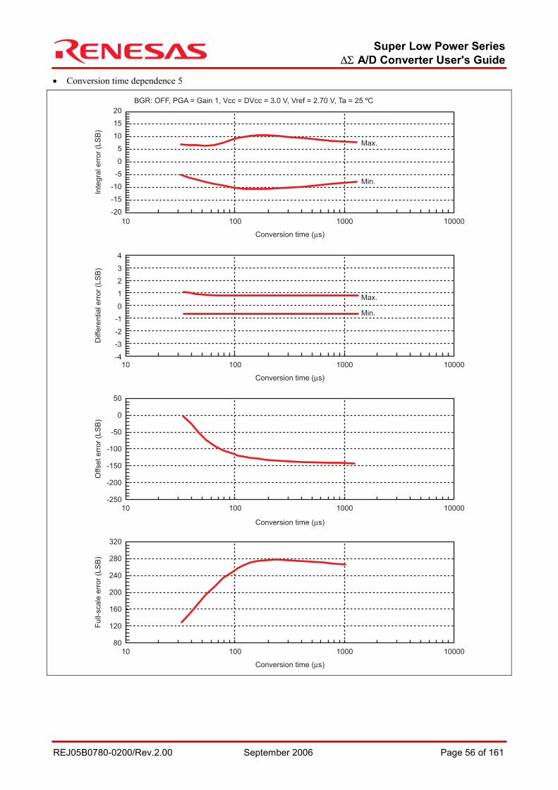
Super Low Power Series ∆Σ A/D Converter User's Guide
REJ05B0780-0200/Rev.2.00 September 2006 Page 56 of 161
• Conversion time dependence 5
Inte
gra
l err
or
(LS
B)
Conversion time (µs)
10010
-20
-15
-10
-5
0
5
10
15
20
1000 10000
BGR: OFF, PGA = Gain 1, Vcc = DVcc = 3.0 V, Vref = 2.70 V, Ta = 25 ºCD
iffe
rential err
or
(LS
B)
Conversion time (µs)
10010-4
-3
-2
-1
0
1
2
3
4
1000 10000
Full-
scale
err
or
(LS
B)
Conversion time (µs)
80
200
160
120
240
280
320
Offset err
or
(LS
B)
Conversion time (µs)
10010 1000 10000
10010 1000 10000
-250
-100
-150
-200
-50
0
50
Max.
Min.
Max.
Min.
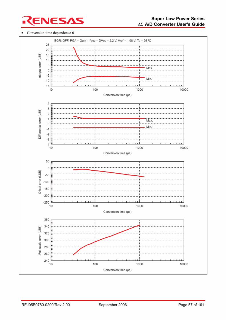
Super Low Power Series ∆Σ A/D Converter User's Guide
REJ05B0780-0200/Rev.2.00 September 2006 Page 57 of 161
• Conversion time dependence 6
Max.
Min.
Max.
Min.
Inte
gra
l e
rro
r (L
SB
)
Conversion time (µs)
10010
25
-15
-10
-5
0
5
10
15
20
1000 10000
BGR: OFF, PGA = Gain 1, Vcc = DVcc = 2.2 V, Vref = 1.98 V, Ta = 25 ºCD
iffe
ren
tia
l e
rro
r (L
SB
)
Conversion time (µs)
10010-4
-3
-2
-1
0
1
2
3
4
1000 10000
Fu
ll-sca
le e
rro
r (L
SB
)
Conversion time (µs)
240
280
260
340
320
300
360
Offset err
or
(LS
B)
Conversion time (µs)
10010 1000 10000
10010 1000 10000
-250
-200
-150
-50
50
-100
0
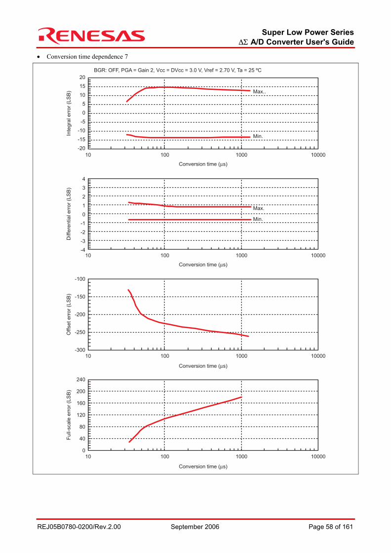
Super Low Power Series ∆Σ A/D Converter User's Guide
REJ05B0780-0200/Rev.2.00 September 2006 Page 58 of 161
• Conversion time dependence 7
Max..
Min.
Max.
Min.
Inte
gra
l e
rro
r (L
SB
)
Conversion time (µs)
10010
-20
-15
-10
-5
0
5
10
15
20
1000 10000
BGR: OFF, PGA = Gain 2, Vcc = DVcc = 3.0 V, Vref = 2.70 V, Ta = 25 ºCD
iffe
ren
tia
l e
rro
r (L
SB
)
Conversion time (µs)
10010-4
-3
-2
-1
0
1
2
3
4
1000 10000
Fu
ll-sca
le e
rro
r (L
SB
)
Conversion time (µs)
0
80
40
200
160
120
240
Offset err
or
(LS
B)
Conversion time (µs)
10010 1000 10000
10010 1000 10000
-300
-250
-200
-150
-100
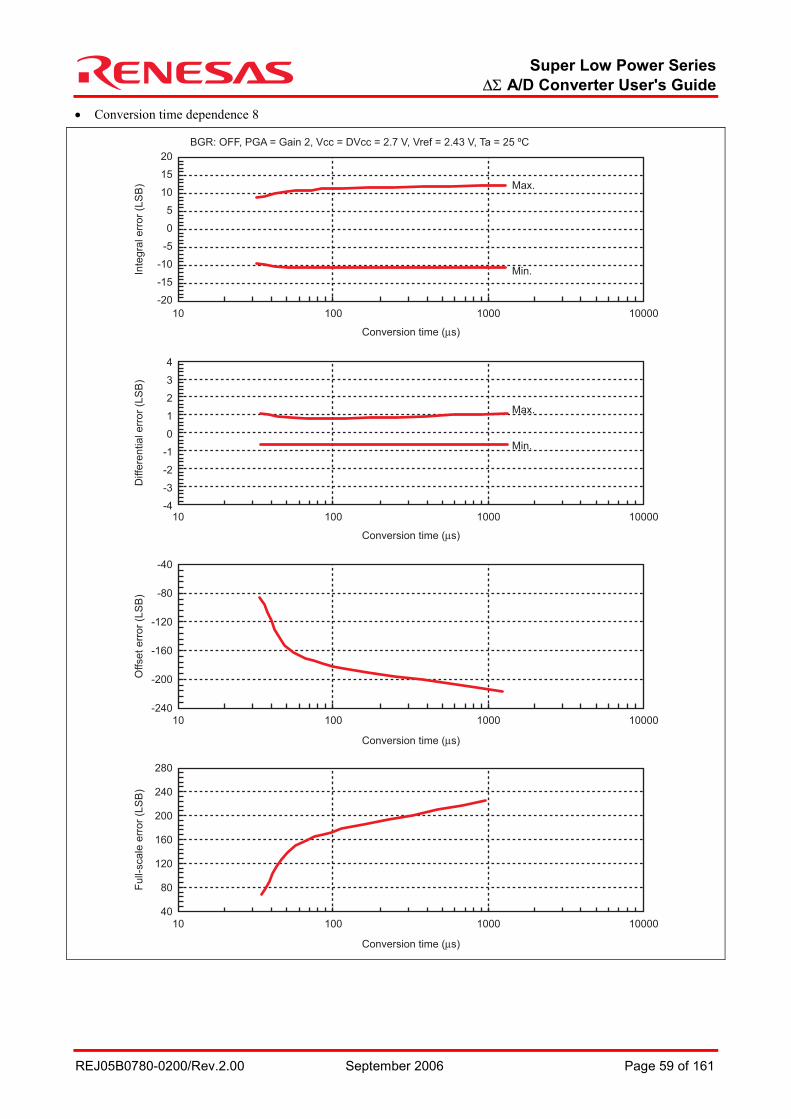
Super Low Power Series ∆Σ A/D Converter User's Guide
REJ05B0780-0200/Rev.2.00 September 2006 Page 59 of 161
• Conversion time dependence 8
Max.
Min.
Max.
Min.
Inte
gra
l e
rro
r (L
SB
)
Conversion time (µs)
10010
-20
-15
-10
-5
0
5
10
15
20
1000 10000
BGR: OFF, PGA = Gain 2, Vcc = DVcc = 2.7 V, Vref = 2.43 V, Ta = 25 ºCD
iffe
ren
tia
l e
rro
r (L
SB
)
Conversion time (µs)
10010-4
-3
-2
-1
0
1
2
3
4
1000 10000
Fu
ll-sca
le e
rro
r (L
SB
)
Conversion time (µs)
40
120
80
240
200
160
280
Offset err
or
(LS
B)
Conversion time (µs)
10010 1000 10000
10010 1000 10000
-240
-200
-160
-120
-80
-40
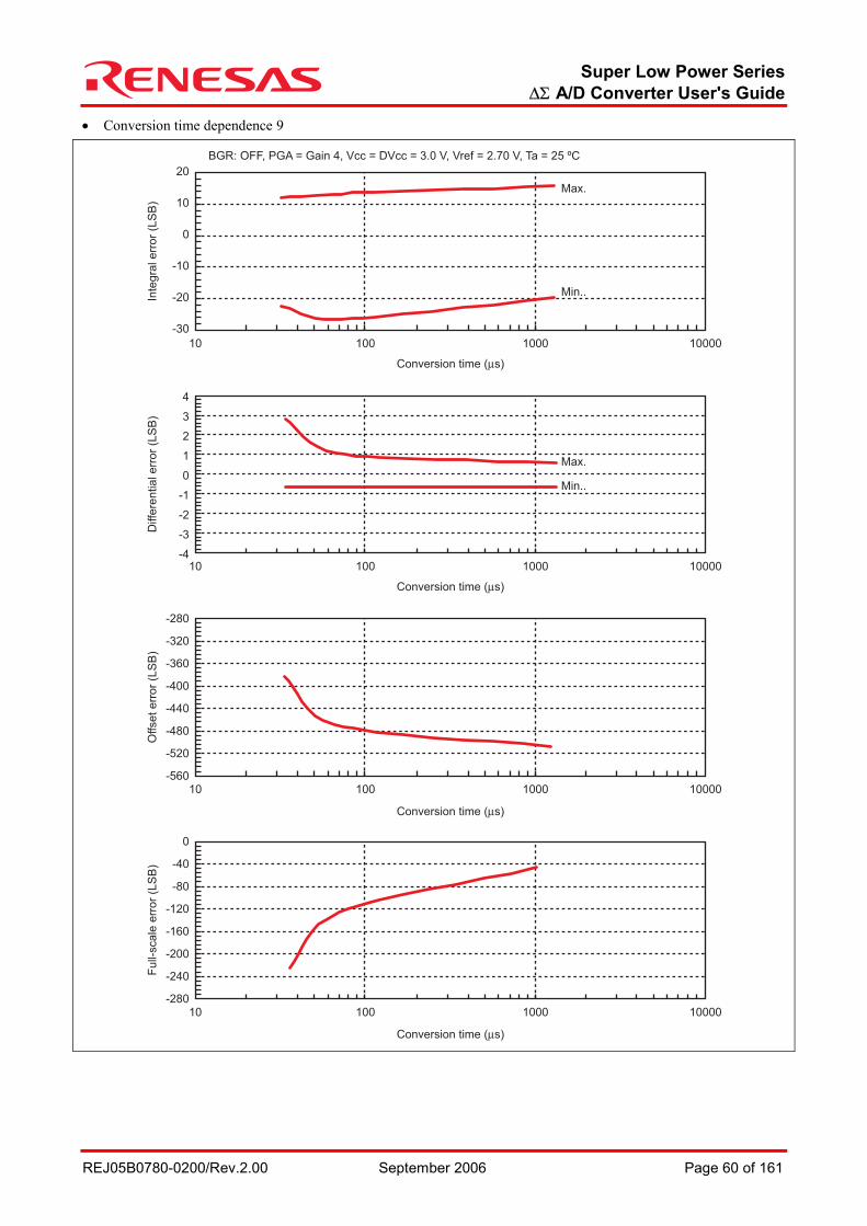
Super Low Power Series ∆Σ A/D Converter User's Guide
REJ05B0780-0200/Rev.2.00 September 2006 Page 60 of 161
• Conversion time dependence 9
Max.
Min..
Max.
Min..
Inte
gra
l e
rro
r (L
SB
)
Conversion time (µs)
10010
-30
-20
-10
0
10
20
1000 10000
BGR: OFF, PGA = Gain 4, Vcc = DVcc = 3.0 V, Vref = 2.70 V, Ta = 25 ºCD
iffe
ren
tia
l e
rro
r (L
SB
)
Conversion time (µs)
10010-4
-3
-2
-1
0
1
2
3
4
1000 10000
Fu
ll-sca
le e
rro
r (L
SB
)
Conversion time (µs)
-280
-200
-240
-80
-40
-120
-160
0
Offset err
or
(LS
B)
Conversion time (µs)
10010 1000 10000
10010 1000 10000
-560
-520
-480
-440
-360
-280
-320
-400
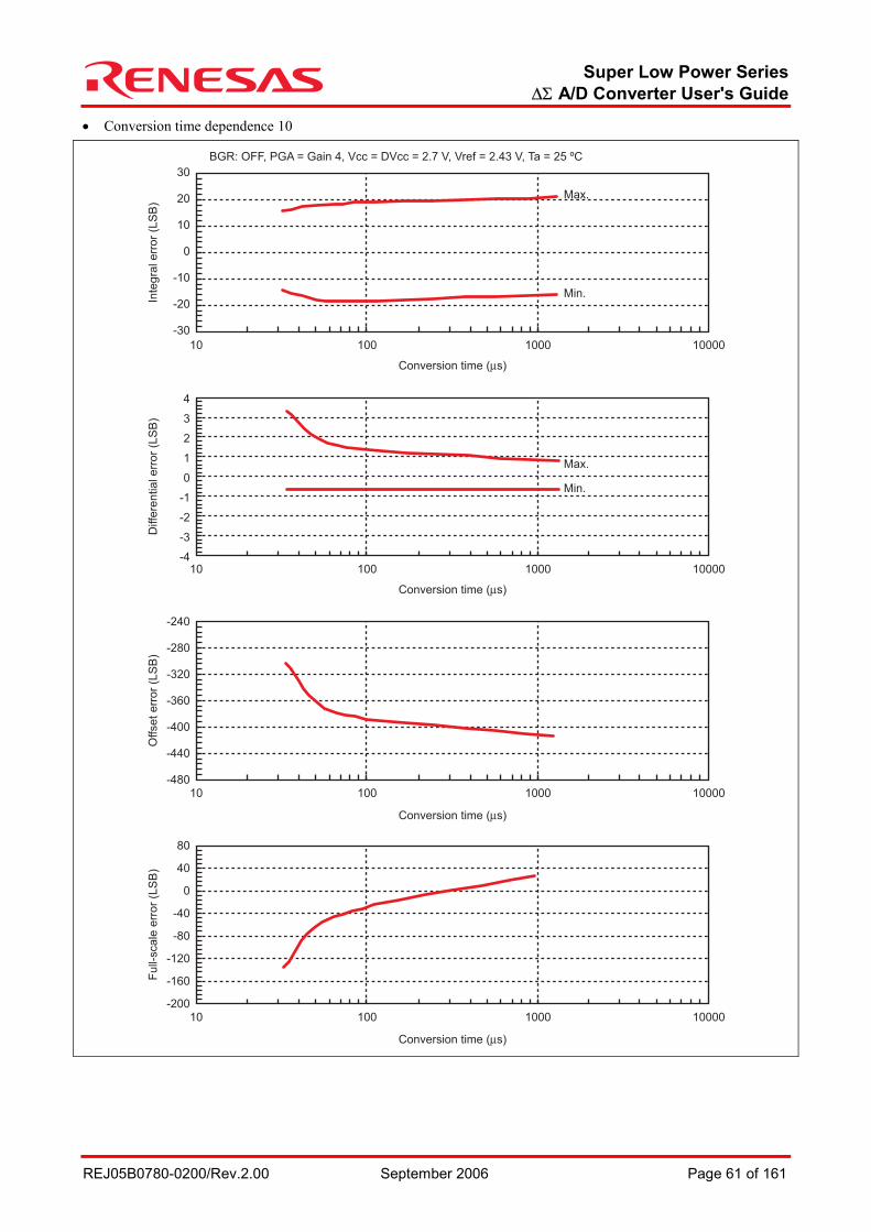
Super Low Power Series ∆Σ A/D Converter User's Guide
REJ05B0780-0200/Rev.2.00 September 2006 Page 61 of 161
• Conversion time dependence 10
Max.
Min.
Max.
Min.
Inte
gra
l e
rro
r (L
SB
)
Conversion time (µs)
10010
-30
-20
-10
0
10
20
30
1000 10000
BGR: OFF, PGA = Gain 4, Vcc = DVcc = 2.7 V, Vref = 2.43 V, Ta = 25 ºCD
iffe
ren
tia
l e
rro
r (L
SB
)
Conversion time (µs)
10010-4
-3
-2
-1
0
1
2
3
4
1000 10000
Fu
ll-sca
le e
rro
r (L
SB
)
Conversion time (µs)
-200
-120
-160
0
40
-40
-80
80
Offset err
or
(LS
B)
Conversion time (µs)
10010 1000 10000
10010 1000 10000
-480
-440
-400
-360
-280
-240
-320
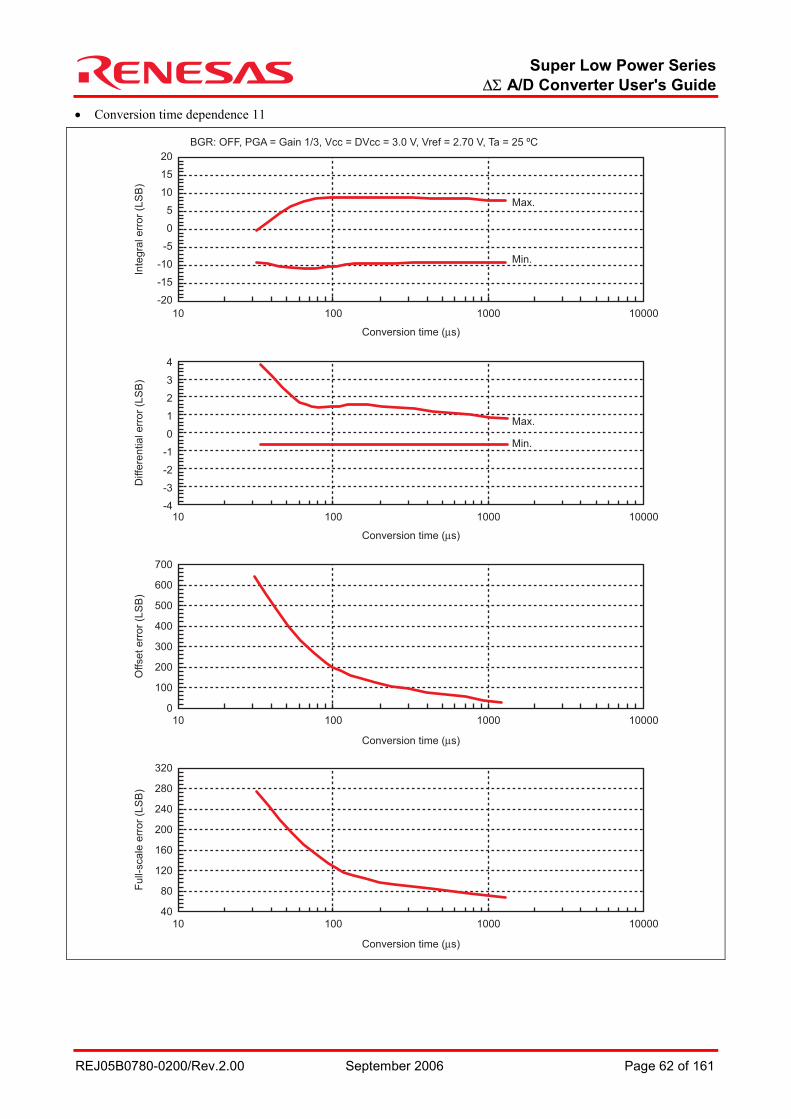
Super Low Power Series ∆Σ A/D Converter User's Guide
REJ05B0780-0200/Rev.2.00 September 2006 Page 62 of 161
• Conversion time dependence 11
Max.
Min.
Max.
Min.
Inte
gra
l e
rro
r (L
SB
)
Conversion time (µs)
10010
-20
-15
-10
-5
0
5
10
15
20
1000 10000
BGR: OFF, PGA = Gain 1/3, Vcc = DVcc = 3.0 V, Vref = 2.70 V, Ta = 25 ºCD
iffe
ren
tia
l e
rro
r (L
SB
)
Conversion time (µs)
10010-4
-3
-2
-1
0
1
2
3
4
1000 10000
Fu
ll-sca
le e
rro
r (L
SB
)
Conversion time (µs)
40
160
120
80
280
240
200
320
Offset err
or
(LS
B)
Conversion time (µs)
10010 1000 10000
10010 1000 10000
0
100
200
300
500
700
400
600
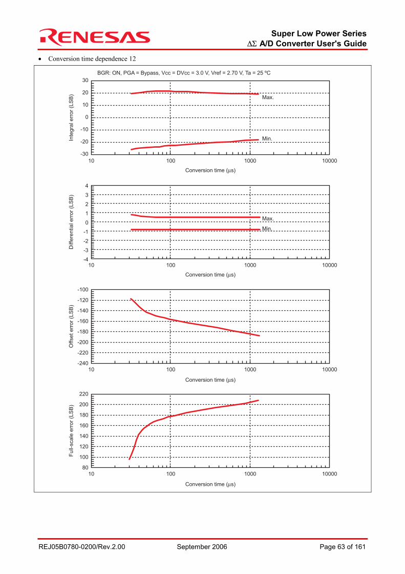
Super Low Power Series ∆Σ A/D Converter User's Guide
REJ05B0780-0200/Rev.2.00 September 2006 Page 63 of 161
• Conversion time dependence 12
Max.
Min.
Max.
Min.
Inte
gra
l e
rro
r (L
SB
)
Conversion time (µs)
10010
-30
-20
-10
0
10
20
30
1000 10000
BGR: ON, PGA = Bypass, Vcc = DVcc = 3.0 V, Vref = 2.70 V, Ta = 25 ºCD
iffe
ren
tia
l e
rro
r (L
SB
)
Conversion time (µs)
10010-4
-3
-2
-1
0
1
2
3
4
1000 10000
Fu
ll-sca
le e
rro
r (L
SB
)
Conversion time (µs)
80
120
100
180
200
160
140
220
Offset err
or
(LS
B)
Conversion time (µs)
10010 1000 10000
10010 1000 10000
-240
-220
-200
-180
-120
-140
-100
-160
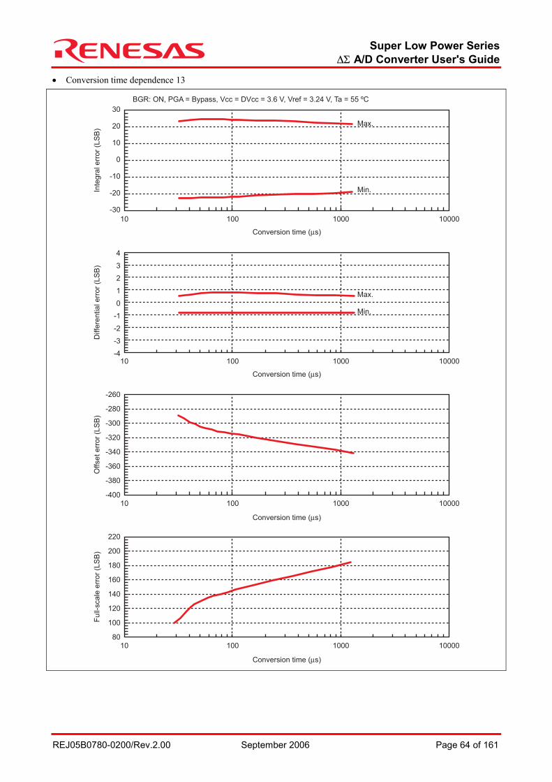
Super Low Power Series ∆Σ A/D Converter User's Guide
REJ05B0780-0200/Rev.2.00 September 2006 Page 64 of 161
• Conversion time dependence 13
Max.
Min.
Max.
Min.
Inte
gra
l e
rro
r (L
SB
)
Conversion time (µs)
10010
-30
-20
-10
0
10
20
30
1000 10000
BGR: ON, PGA = Bypass, Vcc = DVcc = 3.6 V, Vref = 3.24 V, Ta = 55 ºCD
iffe
ren
tia
l e
rro
r (L
SB
)
Conversion time (µs)
10010-4
-3
-2
-1
0
1
2
3
4
1000 10000
Fu
ll-sca
le e
rro
r (L
SB
)
Conversion time (µs)
80
120
100
180
200
160
140
220
Offset err
or
(LS
B)
Conversion time (µs)
10010 1000 10000
10010 1000 10000
-400
-380
-360
-340
-280
-300
-260
-320
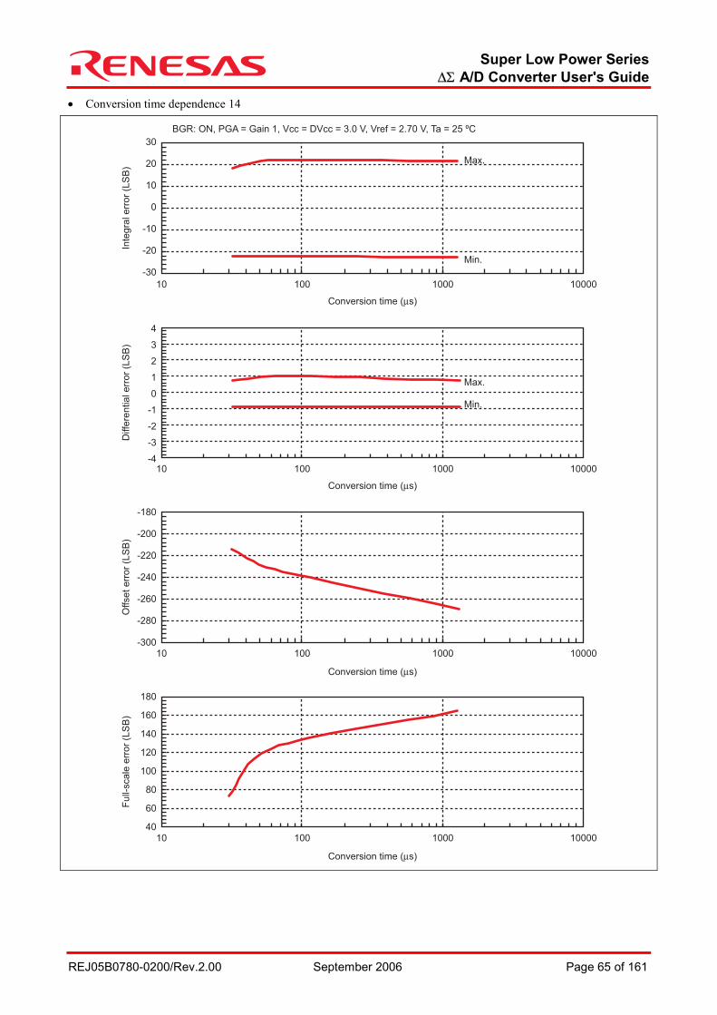
Super Low Power Series ∆Σ A/D Converter User's Guide
REJ05B0780-0200/Rev.2.00 September 2006 Page 65 of 161
• Conversion time dependence 14
Max.
Min.
Max.
Min.
Inte
gra
l e
rro
r (L
SB
)
Conversion time (µs)
10010
-30
-20
-10
0
10
20
30
1000 10000
BGR: ON, PGA = Gain 1, Vcc = DVcc = 3.0 V, Vref = 2.70 V, Ta = 25 ºCD
iffe
ren
tia
l e
rro
r (L
SB
)
Conversion time (µs)
10010-4
-3
-2
-1
0
1
2
3
4
1000 10000
Fu
ll-sca
le e
rro
r (L
SB
)
Conversion time (µs)
40
80
60
140
160
120
100
180
Offset err
or
(LS
B)
Conversion time (µs)
10010 1000 10000
10010 1000 10000
-300
-280
-260
-240
-200
-180
-220
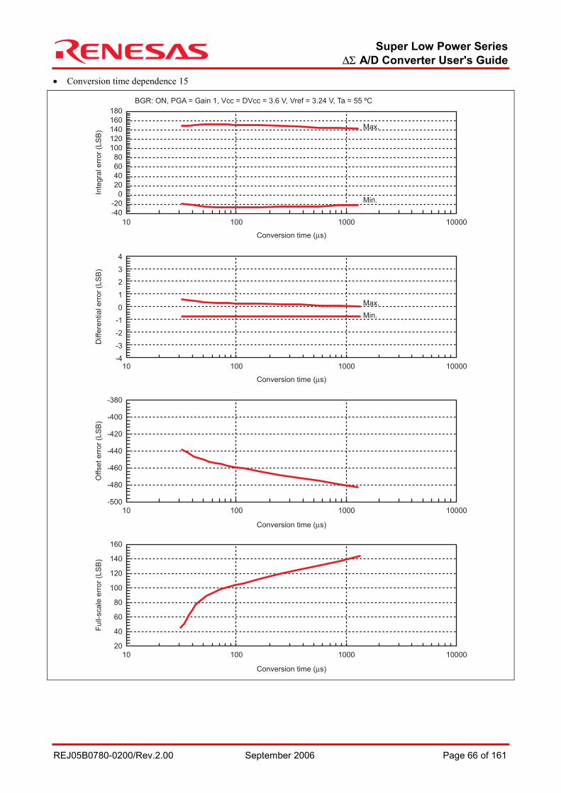
Super Low Power Series ∆Σ A/D Converter User's Guide
REJ05B0780-0200/Rev.2.00 September 2006 Page 66 of 161
• Conversion time dependence 15
Max.
Min.
Max.
Min.
Inte
gra
l e
rro
r (L
SB
)
Conversion time (µs)
10010
-40
0
40
80
120
160
180
-20
20
60
100
140
1000 10000
BGR: ON, PGA = Gain 1, Vcc = DVcc = 3.6 V, Vref = 3.24 V, Ta = 55 ºCD
iffe
ren
tia
l e
rro
r (L
SB
)
Conversion time (µs)
10010-4
-3
-2
-1
0
1
2
3
4
1000 10000
Fu
ll-sca
le e
rro
r (L
SB
)
Conversion time (µs)
20
60
40
120
140
100
80
160
Offset err
or
(LS
B)
Conversion time (µs)
10010 1000 10000
10010 1000 10000
-500
-480
-460
-420
-380
-400
-440
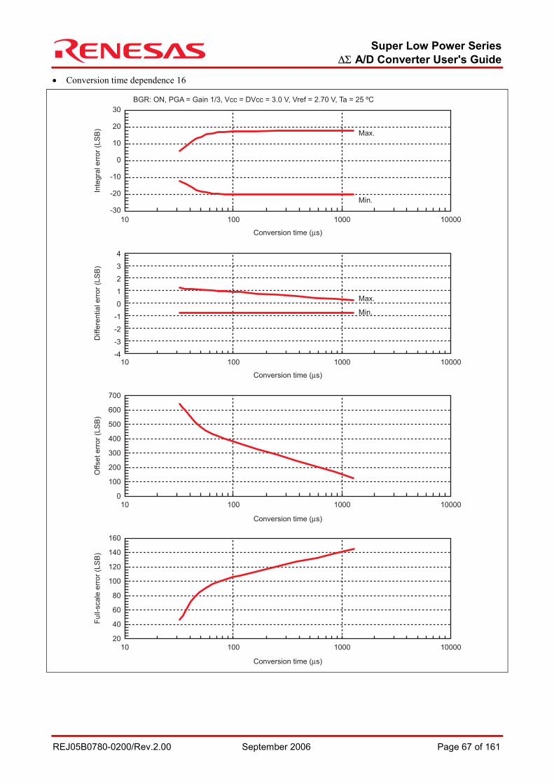
Super Low Power Series ∆Σ A/D Converter User's Guide
REJ05B0780-0200/Rev.2.00 September 2006 Page 67 of 161
• Conversion time dependence 16
Max.
Min.
Max.
Min.
Inte
gra
l e
rro
r (L
SB
)
Conversion time (µs)
10010
-30
-20
-10
0
10
20
30
1000 10000
BGR: ON, PGA = Gain 1/3, Vcc = DVcc = 3.0 V, Vref = 2.70 V, Ta = 25 ºCD
iffe
ren
tia
l e
rro
r (L
SB
)
Conversion time (µs)
10010-4
-3
-2
-1
0
1
2
3
4
1000 10000
Fu
ll-sca
le e
rro
r (L
SB
)
Conversion time (µs)
20
60
40
120
140
100
80
160
Offset err
or
(LS
B)
Conversion time (µs)
10010 1000 10000
10010 1000 10000
0
100
200
300
500
700
600
400
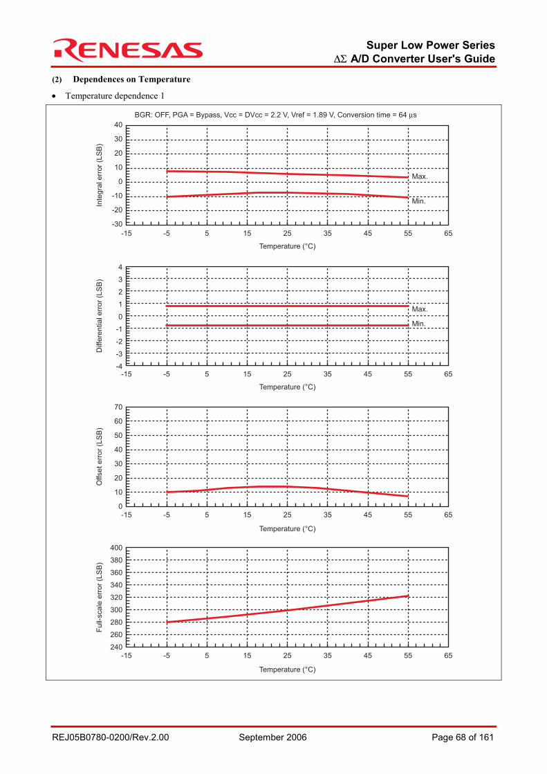
Super Low Power Series ∆Σ A/D Converter User's Guide
REJ05B0780-0200/Rev.2.00 September 2006 Page 68 of 161
(2) Dependences on Temperature
• Temperature dependence 1
Min.
Max.
Max.
Min.
Inte
gra
l e
rro
r (L
SB
)
Temperature (°C)
15-15
-30
-20
-10
0
10
20
40
30
45 655 35-5 25 55
15-15 45 655 35-5 25 55
15-15 45 655 35-5 25 55
15-15 45 655 35-5 25 55
BGR: OFF, PGA = Bypass, Vcc = DVcc = 2.2 V, Vref = 1.89 V, Conversion time = 64 µs
Diffe
ren
tia
l e
rro
r (L
SB
)
Temperature (°C)
-4
-3
-2
-1
0
1
2
3
4
Fu
ll-sca
le e
rro
r (L
SB
)
Temperature (°C)
240
280
260
340
360
320
300
400
380
Offset err
or
(LS
B)
Temperature (°C)
0
10
20
30
50
70
60
40
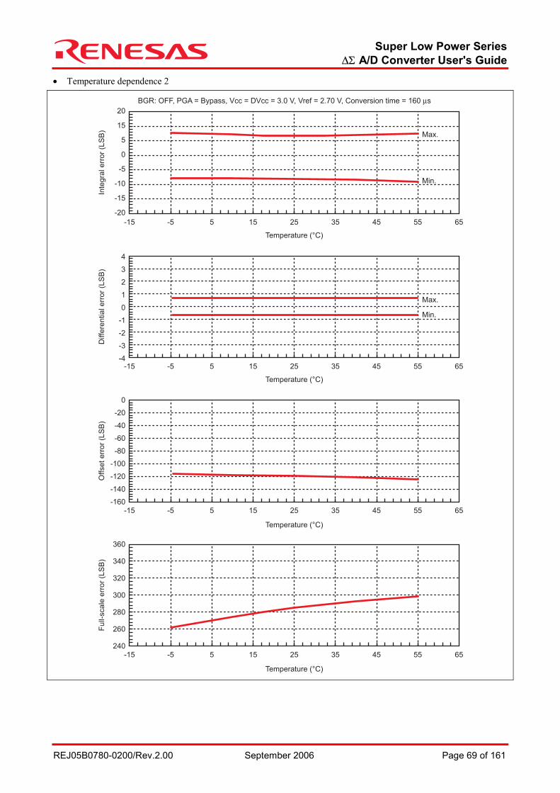
Super Low Power Series ∆Σ A/D Converter User's Guide
REJ05B0780-0200/Rev.2.00 September 2006 Page 69 of 161
• Temperature dependence 2
Max.
Min.
Max.
Min.
Inte
gra
l e
rro
r (L
SB
)
Temperature (°C)
15-15
-20
-15
-10
-5
0
5
20
15
45 655 35-5 25 55
15-15 45 655 35-5 25 55
15-15 45 655 35-5 25 55
15-15 45 655 35-5 25 55
BGR: OFF, PGA = Bypass, Vcc = DVcc = 3.0 V, Vref = 2.70 V, Conversion time = 160 µsD
iffe
ren
tia
l e
rro
r (L
SB
)
Temperature (°C)
-4
-3
-2
-1
0
1
2
3
4
Fu
ll-sca
le e
rro
r (L
SB
)
Temperature (°C)
240
280
260
340
320
300
360
Offset err
or
(LS
B)
Temperature (°C)
-160
-140
-120
-100
-60
0
-20
-40
-80
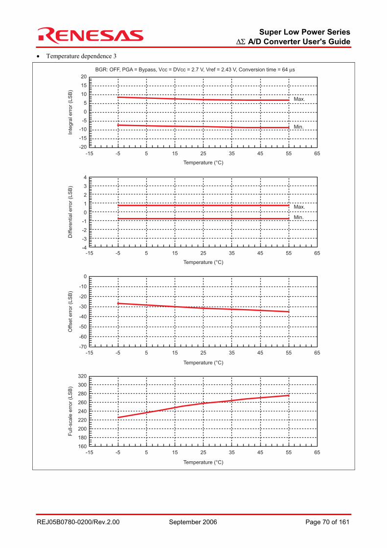
Super Low Power Series ∆Σ A/D Converter User's Guide
REJ05B0780-0200/Rev.2.00 September 2006 Page 70 of 161
• Temperature dependence 3
Max.
Min.
Max.
Min.
Inte
gra
l e
rro
r (L
SB
)
Temperature (°C)
15-15
-20
-10
-15
-5
0
5
10
20
15
45 655 35-5 25 55
15-15 45 655 35-5 25 55
15-15 45 655 35-5 25 55
15-15 45 655 35-5 25 55
BGR: OFF, PGA = Bypass, Vcc = DVcc = 2.7 V, Vref = 2.43 V, Conversion time = 64 µsD
iffe
ren
tia
l e
rro
r (L
SB
)
Temperature (°C)
-4
-3
-2
-1
0
1
2
3
4
Fu
ll-sca
le e
rro
r (L
SB
)
Temperature (°C)
160
200
180
260
280
240
220
320
300
Offset err
or
(LS
B)
Temperature (°C)
-70
-60
-50
-40
-20
0
-10
-30
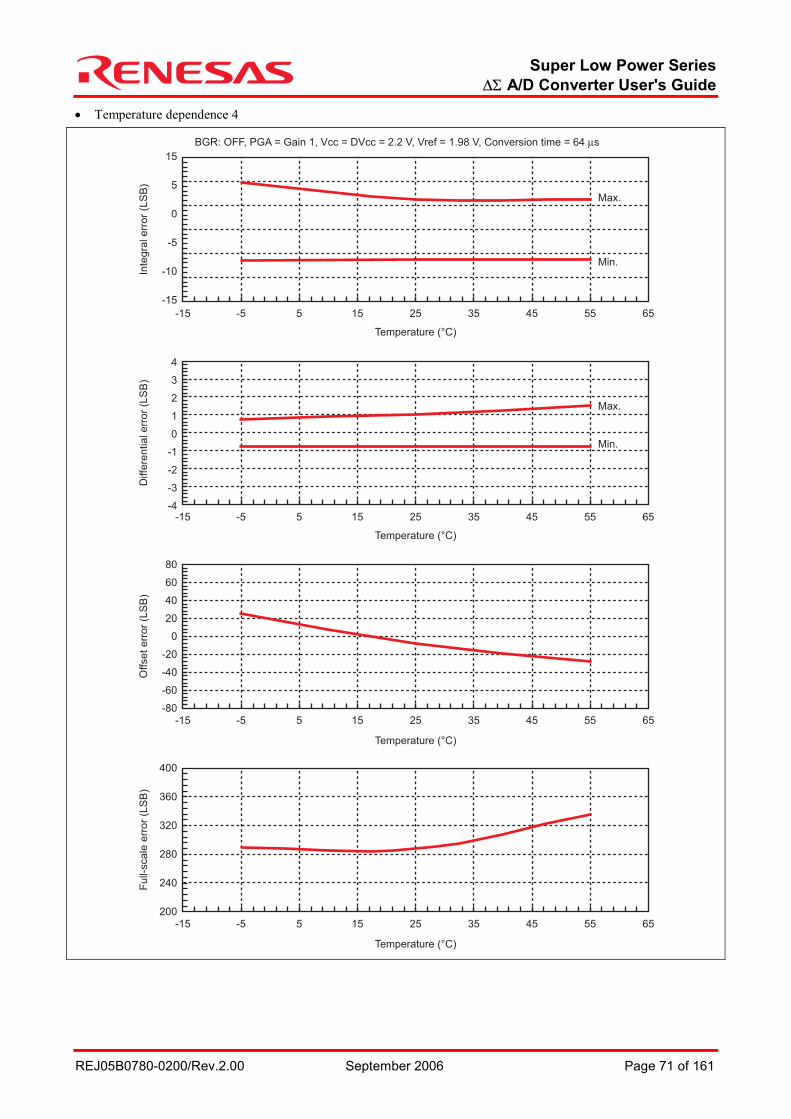
Super Low Power Series ∆Σ A/D Converter User's Guide
REJ05B0780-0200/Rev.2.00 September 2006 Page 71 of 161
• Temperature dependence 4
Max.
Min.
Max.
Min.
Inte
gra
l e
rro
r (L
SB
)
Temperature (°C)
15-15
-15
-10
-5
0
5
15
45 655 35-5 25 55
15-15 45 655 35-5 25 55
15-15 45 655 35-5 25 55
15-15 45 655 35-5 25 55
BGR: OFF, PGA = Gain 1, Vcc = DVcc = 2.2 V, Vref = 1.98 V, Conversion time = 64 µsD
iffe
ren
tia
l e
rro
r (L
SB
)
Temperature (°C)
-4
-3
-2
-1
0
1
2
3
4
Fu
ll-sca
le e
rro
r (L
SB
)
Temperature (°C)
200
240
360
320
280
400
Offset err
or
(LS
B)
Temperature (°C)
-80
-60
-40
-20
20
80
60
40
0
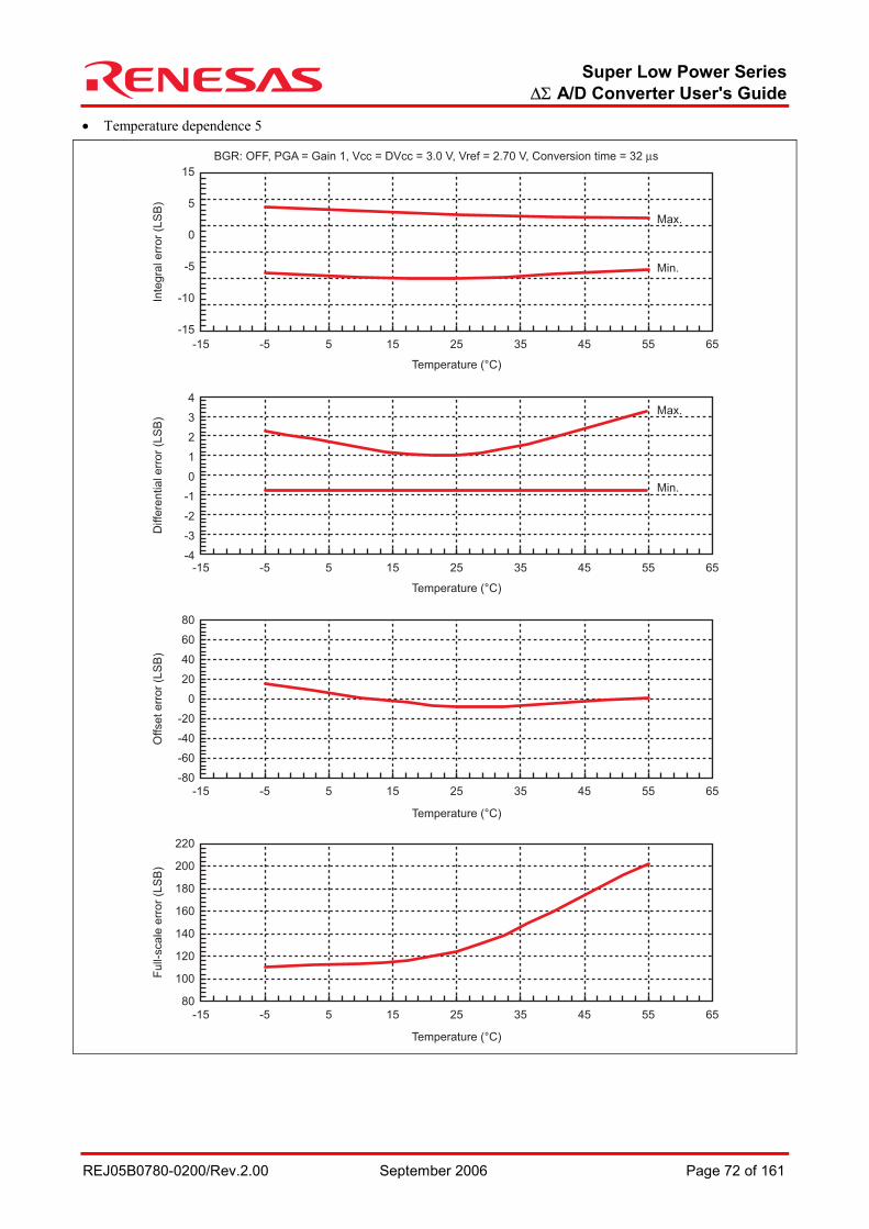
Super Low Power Series ∆Σ A/D Converter User's Guide
REJ05B0780-0200/Rev.2.00 September 2006 Page 72 of 161
• Temperature dependence 5
Inte
gra
l err
or
(LS
B)
Temperature (°C)
Diffe
ren
tia
l e
rro
r (L
SB
)
Temperature (°C)
Fu
ll-sca
le e
rro
r (L
SB
)
Temperature (°C)
Offset err
or
(LS
B)
Temperature (°C)
Max.
Min.
Max.
Min.
15-15
-15
-10
-5
0
5
15
45 655 35-5 25 55
15-15 45 655 35-5 25 55
15-15 45 655 35-5 25 55
15-15 45 655 35-5 25 55
BGR: OFF, PGA = Gain 1, Vcc = DVcc = 3.0 V, Vref = 2.70 V, Conversion time = 32 µs
-4
-3
-2
-1
0
1
2
3
4
80
140
200
180
160
100
120
220
-80
-60
-40
-20
20
80
60
40
0
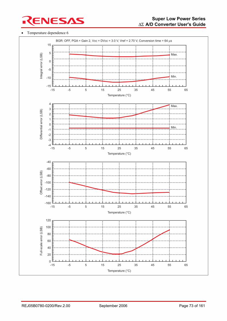
Super Low Power Series ∆Σ A/D Converter User's Guide
REJ05B0780-0200/Rev.2.00 September 2006 Page 73 of 161
• Temperature dependence 6
Inte
gra
l err
or
(LS
B)
Temperature (°C)
Diffe
ren
tia
l e
rro
r (L
SB
)
Temperature (°C)
Fu
ll-sca
le e
rro
r (L
SB
)
Temperature (°C)
Offset err
or
(LS
B)
Temperature (°C)
Max.
Min.
Max.
Min.
15-15
-15
-10
-5
0
5
15
45 655 35-5 25 55
15-15 45 655 35-5 25 55
15-15 45 655 35-5 25 55
15-15 45 655 35-5 25 55
BGR: OFF, PGA = Gain 2, Vcc = DVcc = 3.0 V, Vref = 2.70 V, Conversion time = 64 µs
-4
-3
-2
-1
0
1
2
3
4
0
20
40
100
80
60
120
-160
-140
-120
-100
-60
-40
-80

Super Low Power Series ∆Σ A/D Converter User's Guide
REJ05B0780-0200/Rev.2.00 September 2006 Page 74 of 161
• Temperature dependence 7
Inte
gra
l err
or
(LS
B)
Temperature (°C)
Diffe
ren
tia
l e
rro
r (L
SB
)
Temperature (°C)
Fu
ll-sca
le e
rro
r (L
SB
)
Temperature (°C)
Offset err
or
(LS
B)
Temperature (°C)
Max.
Min.
Max.
Min.
15-15
-15
-10
-5
0
5
15
45 655 35-5 25 55
15-15 45 655 35-5 25 55
15-15 45 655 35-5 25 55
15-15 45 655 35-5 25 55
BGR: OFF, PGA = Gain 2, Vcc = DVcc = 2.7 V, Vref = 2.43 V, Conversion time = 64 µs
-4
-3
-2
-1
0
1
2
3
4
0
20
40
100
80
60
120
-160
-140
-120
-100
-60
-40
-80
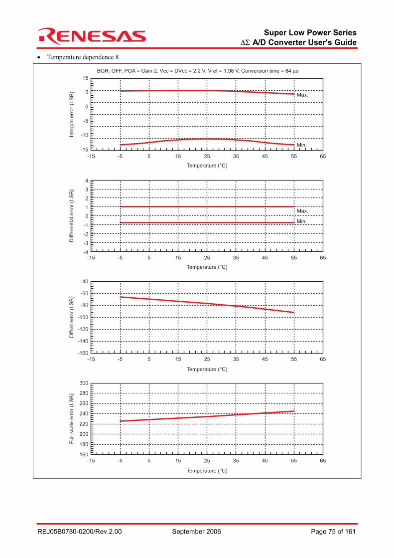
Super Low Power Series ∆Σ A/D Converter User's Guide
REJ05B0780-0200/Rev.2.00 September 2006 Page 75 of 161
• Temperature dependence 8
Inte
gra
l err
or
(LS
B)
Temperature (°C)
Diffe
ren
tia
l e
rro
r (L
SB
)
Temperature (°C)
Fu
ll-sca
le e
rro
r (L
SB
)
Temperature (°C)
Offset err
or
(LS
B)
Temperature (°C)
Max.
Min.
Max.
Min.
15-15
-15
-10
-5
0
5
15
45 655 35-5 25 55
15-15 45 655 35-5 25 55
15-15 45 655 35-5 25 55
15-15 45 655 35-5 25 55
BGR: OFF, PGA = Gain 2, Vcc = DVcc = 2.2 V, Vref = 1.98 V, Conversion time = 64 µs
-4
-3
-2
-1
0
1
2
3
4
160
180
200
220
280
260
240
300
-160
-140
-120
-100
-60
-40
-80
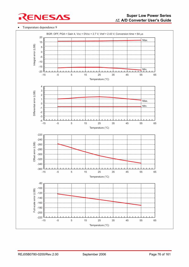
Super Low Power Series ∆Σ A/D Converter User's Guide
REJ05B0780-0200/Rev.2.00 September 2006 Page 76 of 161
• Temperature dependence 9
Inte
gra
l err
or
(LS
B)
Temperature (°C)
Diffe
ren
tia
l e
rro
r (L
SB
)
Temperature (°C)
Fu
ll-sca
le e
rro
r (L
SB
)
Temperature (°C)
Offset err
or
(LS
B)
Temperature (°C)
Max.
Min.
Max.
Min.
15-15
-20
-10
-5
0
5
20
-15
15
45 655 35-5 25 55
15-15 45 655 35-5 25 55
15-15 45 655 35-5 25 55
15-15 45 655 35-5 25 55
BGR: OFF, PGA = Gain 4, Vcc = DVcc = 2.7 V, Vref = 2.43 V, Conversion time = 64 µs
-4
-3
-2
-1
0
1
2
3
4
-220
-200
-180
-160
-100
-120
-140
-80
-360
-340
-320
-260
-220
-280
-240
-300
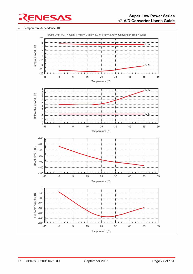
Super Low Power Series ∆Σ A/D Converter User's Guide
REJ05B0780-0200/Rev.2.00 September 2006 Page 77 of 161
• Temperature dependence 10
Inte
gra
l err
or
(LS
B)
Temperature (°C)
Diffe
ren
tia
l e
rro
r (L
SB
)
Temperature (°C)
Fu
ll-sca
le e
rro
r (L
SB
)
Temperature (°C)
Offset err
or
(LS
B)
Temperature (°C)
Max.
Min.
Max.
Min.
15-15
-25
-20
-10
-5
0
5
20
-15
15
45 655 35-5 25 55
15-15 45 655 35-5 25 55
15-15 45 655 35-5 25 55
15-15 45 655 35-5 25 55
BGR: OFF, PGA = Gain 4, Vcc = DVcc = 3.0 V, Vref = 2.70 V, Conversion time = 32 µs
-4-3-2-1
1
3
5
78
0
2
4
6
-280
-240
-200
-160
-40
-80
-120
0
-480
-440
-400
-280
-240
-320
-360
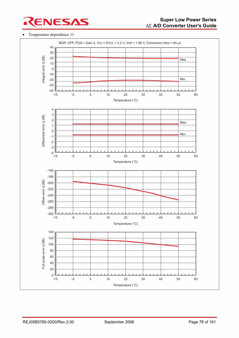
Super Low Power Series ∆Σ A/D Converter User's Guide
REJ05B0780-0200/Rev.2.00 September 2006 Page 78 of 161
• Temperature dependence 11
Inte
gra
l err
or
(LS
B)
Temperature (°C)
Diffe
ren
tia
l e
rro
r (L
SB
)
Temperature (°C)
Fu
ll-sca
le e
rro
r (L
SB
)
Temperature (°C)
Offset err
or
(LS
B)
Temperature (°C)
Max.
Min.
Max.
Min.
-4
-3
-2
-1
0
1
2
3
4
15-15
-40
-30
-10
0
10
20
40
-20
30
45 655 35-5 25 55
15-15 45 655 35-5 25 55
15-15 45 655 35-5 25 55
15-15 45 655 35-5 25 55
BGR: OFF, PGA = Gain 4, Vcc = DVcc = 2.2 V, Vref = 1.98 V, Conversion time = 64 µs
0
20
40
60
120
100
80
140
-300
-260
-280
-240
-180
-160
-200
-220
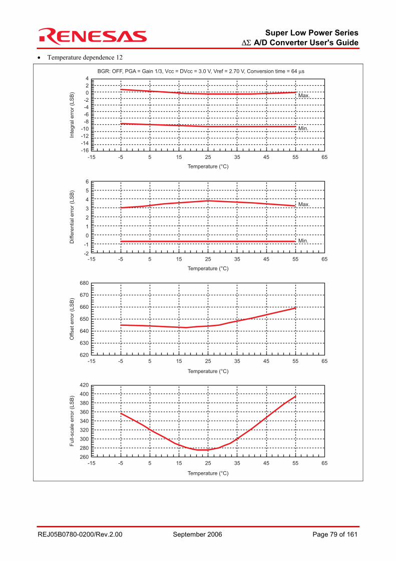
Super Low Power Series ∆Σ A/D Converter User's Guide
REJ05B0780-0200/Rev.2.00 September 2006 Page 79 of 161
• Temperature dependence 12
Inte
gra
l err
or
(LS
B)
Temperature (°C)
Diffe
ren
tia
l e
rro
r (L
SB
)
Temperature (°C)
Fu
ll-sca
le e
rro
r (L
SB
)
Temperature (°C)
Offset err
or
(LS
B)
Temperature (°C)
-2
-1
0
1
2
3
4
5
6
15-15
-16
-14
-12
-8
-6
-4
-2
4
-10
0
2
45 655 35-5 25 55
15-15 45 655 35-5 25 55
15-15 45 655 35-5 25 55
15-15 45 655 35-5 25 55
BGR: OFF, PGA = Gain 1/3, Vcc = DVcc = 3.0 V, Vref = 2.70 V, Conversion time = 64 µs
260
280
300
320
340
400
380
360
420
620
630
640
670
680
660
650
Max.
Min.
Max.
Min.
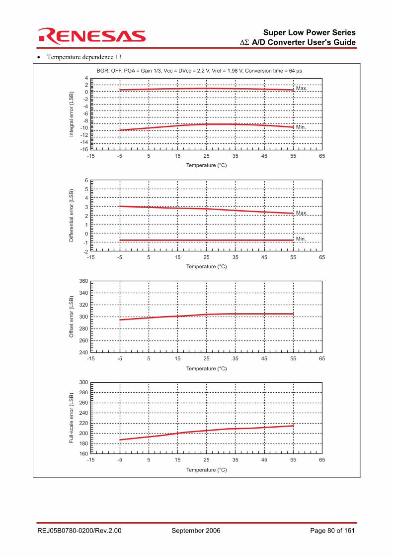
Super Low Power Series ∆Σ A/D Converter User's Guide
REJ05B0780-0200/Rev.2.00 September 2006 Page 80 of 161
• Temperature dependence 13
Inte
gra
l err
or
(LS
B)
Temperature (°C)
Diffe
ren
tia
l e
rro
r (L
SB
)
Temperature (°C)
Fu
ll-sca
le e
rro
r (L
SB
)
Temperature (°C)
Offset err
or
(LS
B)
Temperature (°C)
Max.
Min.
Max.
Min.
-2
-1
0
1
2
3
4
5
6
15-15
-16
-14
-12
-8
-6
-4
-2
4
-10
0
2
45 655 35-5 25 55
15-15 45 655 35-5 25 55
15-15 45 655 35-5 25 55
15-15 45 655 35-5 25 55
BGR: OFF, PGA = Gain 1/3, Vcc = DVcc = 2.2 V, Vref = 1.98 V, Conversion time = 64 µs
160
180
200
220
280
260
240
300
240
260
280
340
360
320
300
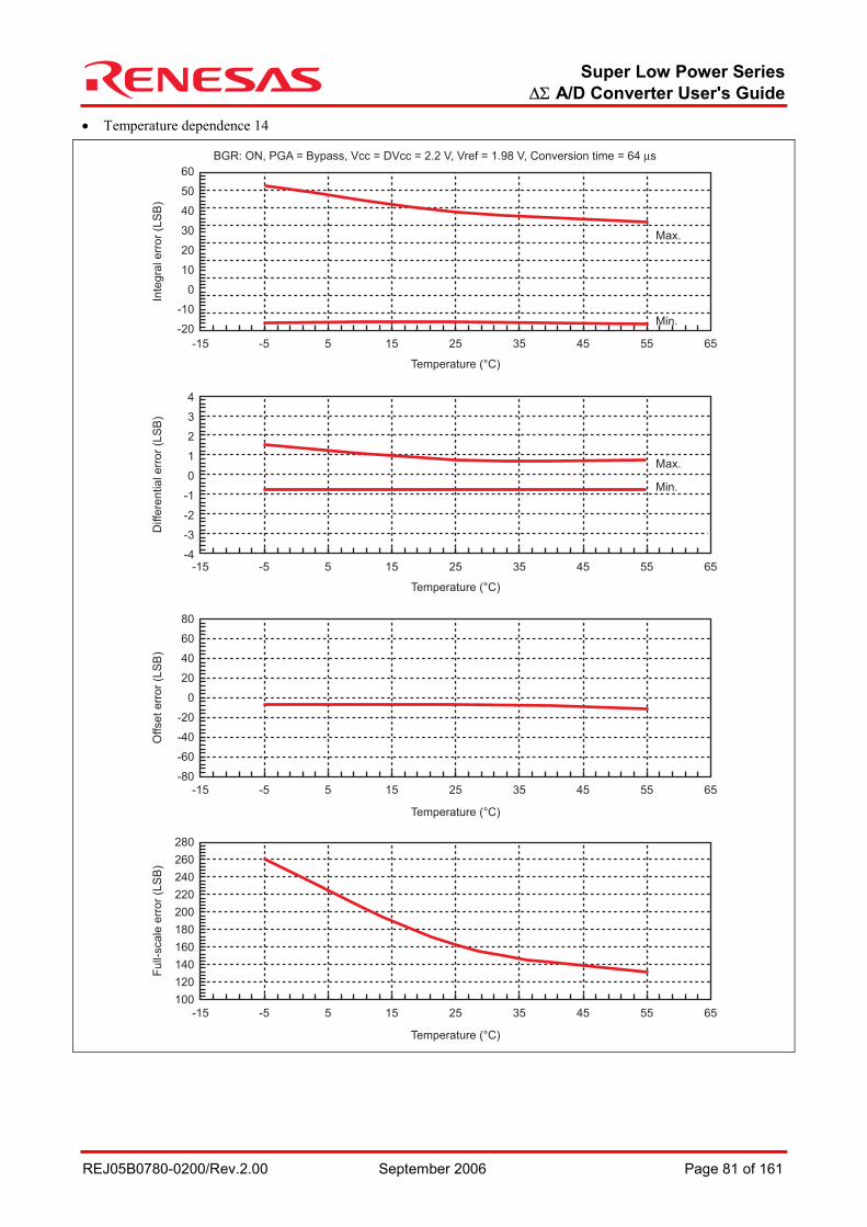
Super Low Power Series ∆Σ A/D Converter User's Guide
REJ05B0780-0200/Rev.2.00 September 2006 Page 81 of 161
• Temperature dependence 14
Inte
gra
l err
or
(LS
B)
Temperature (°C)
Diffe
ren
tia
l e
rro
r (L
SB
)
Temperature (°C)
Fu
ll-sca
le e
rro
r (L
SB
)
Temperature (°C)
Offset err
or
(LS
B)
Temperature (°C)
Max.
Min.
Max.
Min.
-4
-3
-2
-1
0
1
2
3
4
15-15
-20
0
10
20
30
60
-10
40
50
45 655 35-5 25 55
15-15 45 655 35-5 25 55
15-15 45 655 35-5 25 55
15-15 45 655 35-5 25 55
BGR: ON, PGA = Bypass, Vcc = DVcc = 2.2 V, Vref = 1.98 V, Conversion time = 64 µs
100
120
140
160
240
200
180
280
220
260
-80
-20
60
80
40
20
0
-40
-60
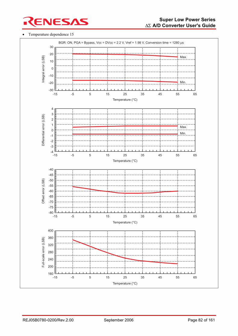
Super Low Power Series ∆Σ A/D Converter User's Guide
REJ05B0780-0200/Rev.2.00 September 2006 Page 82 of 161
• Temperature dependence 15
Inte
gra
l err
or
(LS
B)
Temperature (°C)
Diffe
ren
tia
l e
rro
r (L
SB
)
Temperature (°C)
Fu
ll-sca
le e
rro
r (L
SB
)
Temperature (°C)
Offset err
or
(LS
B)
Temperature (°C)
Max.
Min.
Max.
Min.
-4
-3
-2
-1
0
1
2
3
4
15-15
-30
-10
0
10
20
30
-20
45 655 35-5 25 55
15-15 45 655 35-5 25 55
15-15 45 655 35-5 25 55
15-15 45 655 35-5 25 55
BGR: ON, PGA = Bypass, Vcc = DVcc = 2.2 V, Vref = 1.98 V, Conversion time = 1280 µs
160
320
240
200
400
280
360
-80
-65
-45
-40
-50
-55
-60
-70
-75
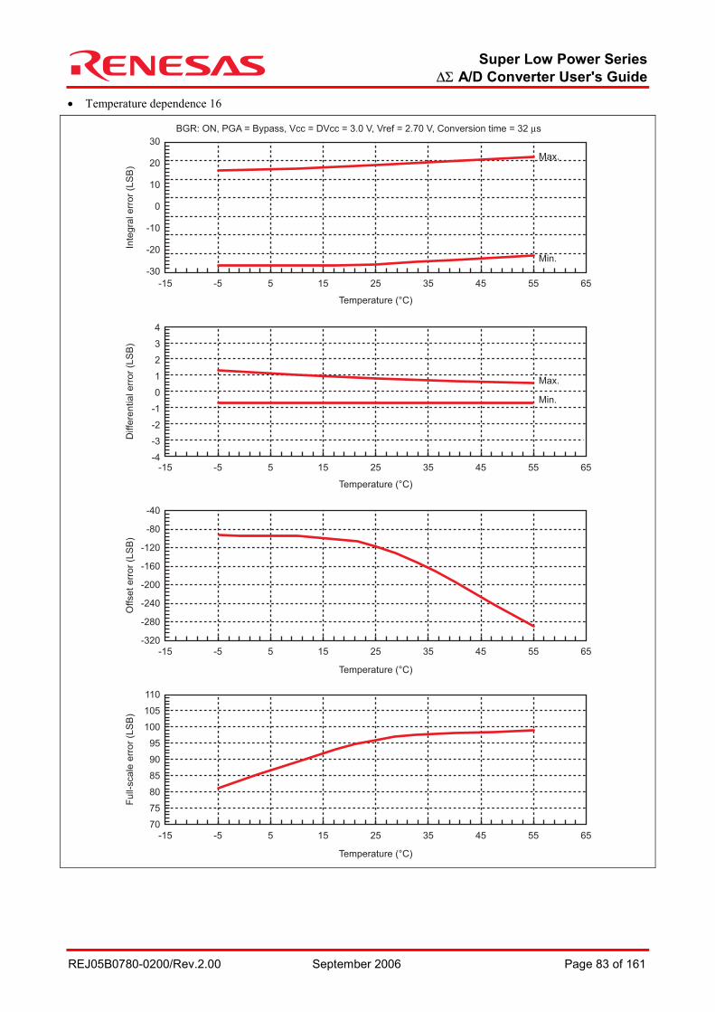
Super Low Power Series ∆Σ A/D Converter User's Guide
REJ05B0780-0200/Rev.2.00 September 2006 Page 83 of 161
• Temperature dependence 16
Inte
gra
l err
or
(LS
B)
Temperature (°C)
Diffe
ren
tia
l e
rro
r (L
SB
)
Temperature (°C)
Fu
ll-sca
le e
rro
r (L
SB
)
Temperature (°C)
Offset err
or
(LS
B)
Temperature (°C)
Max.
Min.
Max.
Min.
-4
-3
-2
-1
0
1
2
3
4
15-15
-30
-10
0
10
20
30
-20
45 655 35-5 25 55
15-15 45 655 35-5 25 55
15-15 45 655 35-5 25 55
15-15 45 655 35-5 25 55
BGR: ON, PGA = Bypass, Vcc = DVcc = 3.0 V, Vref = 2.70 V, Conversion time = 32 µs
70
100
90
85
80
75
110
95
105
-320
-240
-80
-40
-120
-160
-200
-280
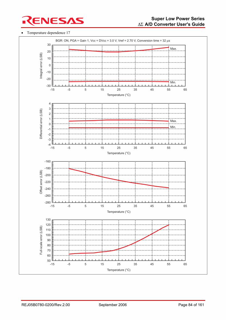
Super Low Power Series ∆Σ A/D Converter User's Guide
REJ05B0780-0200/Rev.2.00 September 2006 Page 84 of 161
• Temperature dependence 17
Inte
gra
l err
or
(LS
B)
Temperature (°C)
Diffe
ren
tia
l e
rro
r (L
SB
)
Temperature (°C)
Fu
ll-sca
le e
rro
r (L
SB
)
Temperature (°C)
Offset err
or
(LS
B)
Temperature (°C)
Max.
Min.
Max.
Min.
-4
-3
-2
-1
0
1
2
3
4
15-15
-30
-10
0
10
20
30
-20
45 655 35-5 25 55
15-15 45 655 35-5 25 55
15-15 45 655 35-5 25 55
15-15 45 655 35-5 25 55
BGR: ON, PGA = Gain 1, Vcc = DVcc = 3.0 V, Vref = 2.70 V, Conversion time = 32 µs
50
110
90
80
70
60
130
100
120
-280
-260
-180
-160
-200
-220
-240
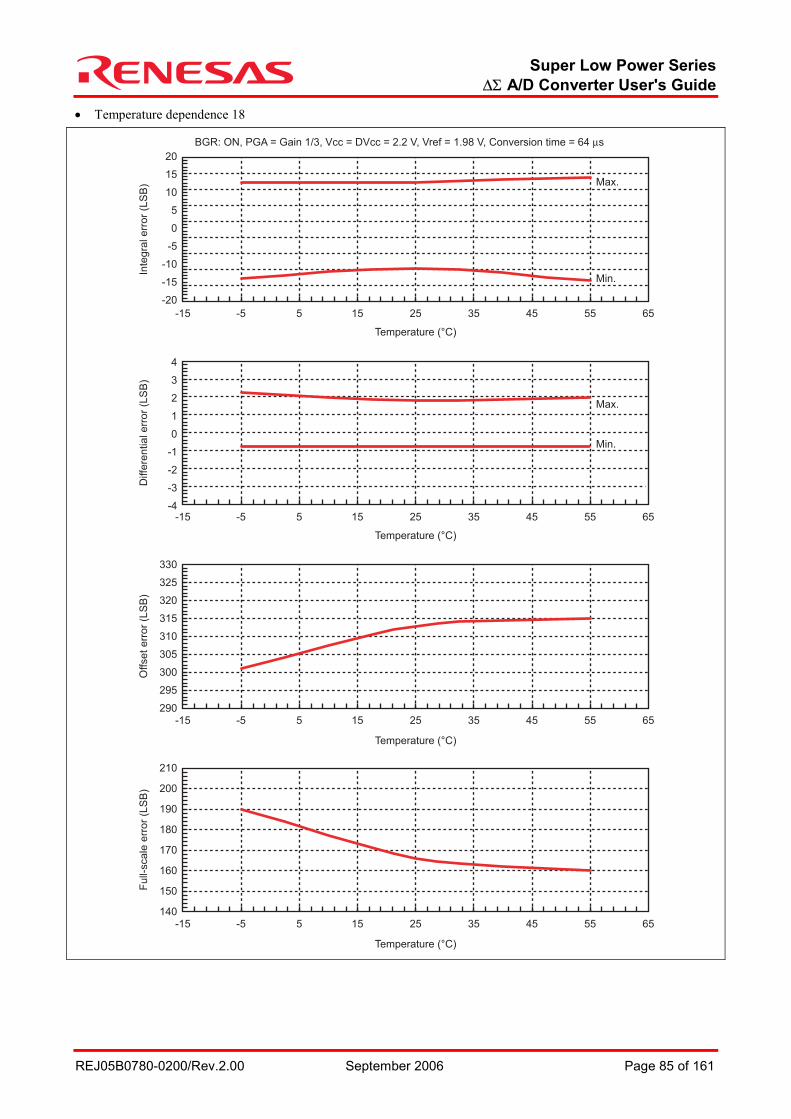
Super Low Power Series ∆Σ A/D Converter User's Guide
REJ05B0780-0200/Rev.2.00 September 2006 Page 85 of 161
• Temperature dependence 18
Inte
gra
l err
or
(LS
B)
Temperature (°C)
Diffe
ren
tia
l e
rro
r (L
SB
)
Temperature (°C)
Fu
ll-sca
le e
rro
r (L
SB
)
Temperature (°C)
Offset err
or
(LS
B)
Temperature (°C)
Max.
Min.
Max.
Min.
-4
-3
-2
-1
0
1
2
3
4
15-15
-20
-5
-10
0
5
10
15
20
-15
45 655 35-5 25 55
15-15 45 655 35-5 25 55
15-15 45 655 35-5 25 55
15-15 45 655 35-5 25 55
BGR: ON, PGA = Gain 1/3, Vcc = DVcc = 2.2 V, Vref = 1.98 V, Conversion time = 64 µs
140
200
180
170
160
150
210
190
290
295
325
330
315
320
310
305
300
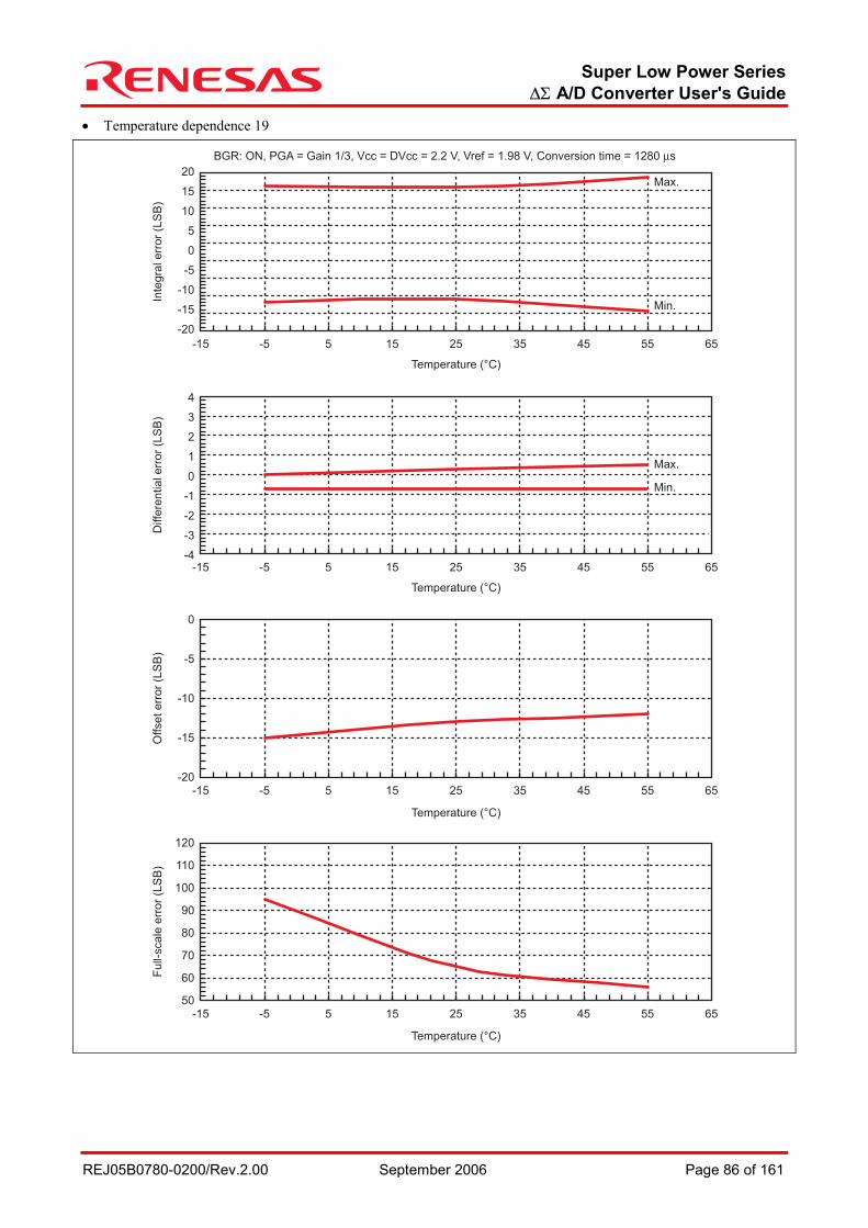
Super Low Power Series ∆Σ A/D Converter User's Guide
REJ05B0780-0200/Rev.2.00 September 2006 Page 86 of 161
• Temperature dependence 19
Max.
Min.
Max.
Min.
-4
-3
-2
-1
0
1
2
3
4
15-15
-20
-5
-10
0
5
10
15
20
-15
45 655 35-5 25 55
15-15 45 655 35-5 25 55
15-15 45 655 35-5 25 55
15-15 45 655 35-5 25 55
BGR: ON, PGA = Gain 1/3, Vcc = DVcc = 2.2 V, Vref = 1.98 V, Conversion time = 1280 µs
50
110
90
80
70
60
120
100
-20
-5
0
-15
-10
Inte
gra
l e
rro
r (L
SB
)
Temperature (°C)
Diffe
ren
tia
l e
rro
r (L
SB
)
Temperature (°C)
Fu
ll-sca
le e
rro
r (L
SB
)
Temperature (°C)
Offset
err
or
(LS
B)
Temperature (°C)

Super Low Power Series ∆Σ A/D Converter User's Guide
REJ05B0780-0200/Rev.2.00 September 2006 Page 87 of 161
• Temperature dependence 20
Inte
gra
l err
or
(LS
B)
Temperature (°C)
Diffe
ren
tia
l e
rro
r (L
SB
)
Temperature (°C)
Fu
ll-sca
le e
rro
r (L
SB
)
Temperature (°C)
Offset err
or
(LS
B)
Temperature (°C)
Max.
Min.
Max.
Min.
-4
-3
-2
-1
0
1
2
3
4
15-15
-20
-5
-10
0
5
10
15
20
-15
45 655 35-5 25 55
15-15 45 655 35-5 25 55
15-15 45 655 35-5 25 55
15-15 45 655 35-5 25 55
BGR: ON, PGA = Gain 1/3, Vcc = DVcc = 3.0 V, Vref = 2.70 V, Conversion time = 32 µs
220
250
255
240
235
230
225
260
245
600
660
680
620
640
650
670
610
630
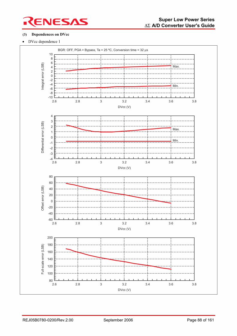
Super Low Power Series ∆Σ A/D Converter User's Guide
REJ05B0780-0200/Rev.2.00 September 2006 Page 88 of 161
(3) Dependences on DVcc
• DVcc dependence 1 In
tegra
l err
or
(LS
B)
Diffe
rential err
or
(LS
B)
Full-
scale
err
or
(LS
B)
Offset err
or
(LS
B)
Max.
Min.
Max.
Min.
-4
-3
-2
-1
0
1
2
3
4
DVcc (V)
3.22.6
2.6
2.6
2.6
-10
-2
-4
0
2
4
8
10
-6
6
-8
3.83 3.62.8 3.4
BGR: OFF, PGA = Bypass, Ta = 25 ºC, Conversion time = 32 µs
80
160
140
120
100
200
180
-60
60
80
-20
20
40
-40
0
DVcc (V)
3.2 3.83 3.62.8 3.4
DVcc (V)
3.2 3.83 3.62.8 3.4
DVcc (V)
3.2 3.83 3.62.8 3.4

Super Low Power Series ∆Σ A/D Converter User's Guide
REJ05B0780-0200/Rev.2.00 September 2006 Page 89 of 161
• DVcc dependence 2
Inte
gra
l err
or
(LS
B)
Diffe
rential err
or
(LS
B)
Full-
scale
err
or
(LS
B)
Offset err
or
(LS
B)
DVcc (V)
DVcc (V)
DVcc (V)
DVcc (V)
Max.
Min.
Max.
Min.
-4
-3
-2
-1
0
1
2
3
4
2.62
-10
-2
-4
0
2
4
8
10
-6
6
-8
3.22.4 32.2 2.8
2.62 2.4 32.2 2.8
2.62 2.4 32.2 2.8
2.62 2.4 32.2 2.8
BGR: OFF, PGA = Bypass, Ta = 25 ºC, Conversion time = 64 µs
200
280
260
240
220
320
300
-80
20
40
-60
-20
0
-40
3.2
3.2
3.2
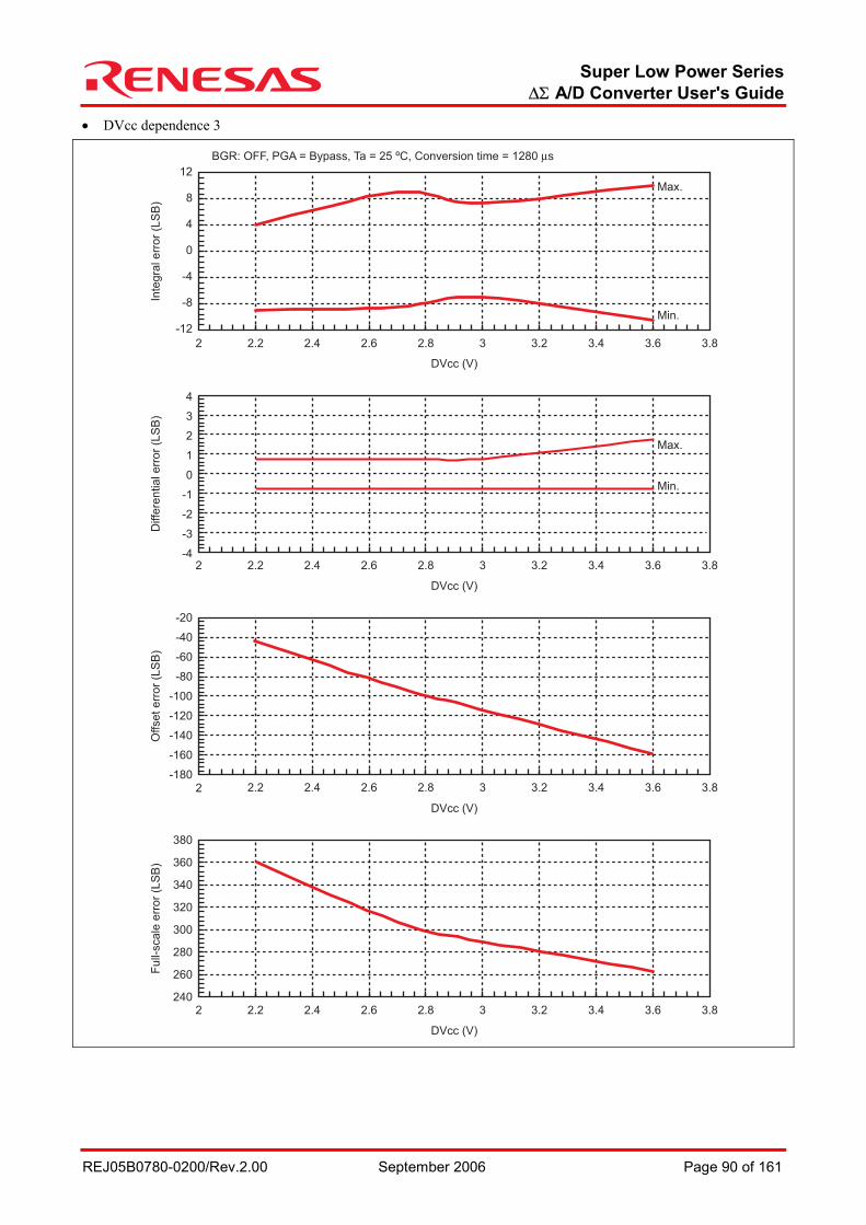
Super Low Power Series ∆Σ A/D Converter User's Guide
REJ05B0780-0200/Rev.2.00 September 2006 Page 90 of 161
• DVcc dependence 3
Inte
gra
l err
or
(LS
B)
Diffe
rential err
or
(LS
B)
Full-
scale
err
or
(LS
B)
Offset err
or
(LS
B)
DVcc (V)
DVcc (V)
DVcc (V)
DVcc (V)
Max.
Min.
Max.
Min.
-4
-3
-2
-1
0
1
2
3
4
2.62
-12
-4
0
4
8
12
-8
3.22.4 32.2 2.8
2
BGR: OFF, PGA = Bypass, Ta = 25 ºC, Conversion time = 1280 µs
3.83.63.4
2.62 3.22.4 32.2 2.8 3.83.63.4
2.6 3.22.4 32.2 2.8 3.83.63.4
2.62 3.22.4 32.2 2.8 3.83.63.4240
320
300
280
260
380
340
360
-180
-40
-80
-60
-20
-160
-120
-100
-140
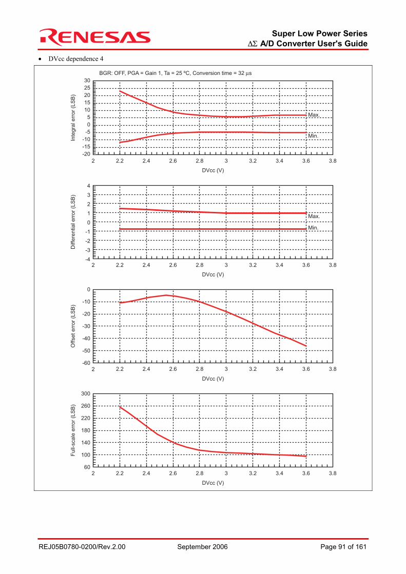
Super Low Power Series ∆Σ A/D Converter User's Guide
REJ05B0780-0200/Rev.2.00 September 2006 Page 91 of 161
• DVcc dependence 4
Inte
gra
l err
or
(LS
B)
Diffe
rential err
or
(LS
B)
Full-
scale
err
or
(LS
B)
Offset err
or
(LS
B)
DVcc (V)
DVcc (V)
DVcc (V)
DVcc (V)
2.62
-20
-5
5
15
25
-10
0
10
20
30
-15
3.22.4 32.2 2.8 3.83.63.4
2
2.62 3.22.4 32.2 2.8 3.83.63.4
2.6 3.22.4 32.2 2.8 3.83.63.4
2.62 3.22.4 32.2 2.8 3.83.63.4
Max.
Min.
Max.
Min.
-4
-3
-2
-1
0
1
2
3
4
BGR: OFF, PGA = Gain 1, Ta = 25 ºC, Conversion time = 32 µs
60
220
180
140
100
300
260
-60
-10
0
-50
-30
-20
-40
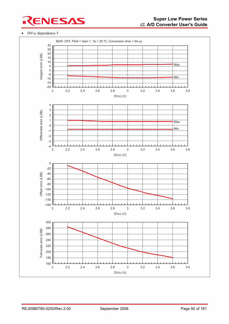
Super Low Power Series ∆Σ A/D Converter User's Guide
REJ05B0780-0200/Rev.2.00 September 2006 Page 92 of 161
• DVcc dependence 5
Inte
gra
l err
or
(LS
B)
Diffe
rential err
or
(LS
B)
Full-
scale
err
or
(LS
B)
Offset err
or
(LS
B)
DVcc (V)
DVcc (V)
DVcc (V)
DVcc (V)
Max.
Min.
Max.
Min.
-4
-3
-2
-1
0
1
2
3
4
2.62
-20
-5
5
15
25
-10
0
10
20
30
-15
3.22.4 32.2 2.8
2
BGR: OFF, PGA = Gain 1, Ta = 25 ºC, Conversion time = 64 µs
3.83.63.4
2.62 3.22.4 32.2 2.8 3.83.63.4
2.6 3.22.4 32.2 2.8 3.83.63.4
2.62 3.22.4 32.2 2.8 3.83.63.4160
240
220
200
180
300
260
280
-40
-80
-60
-20
0
-160
-120
-100
-140
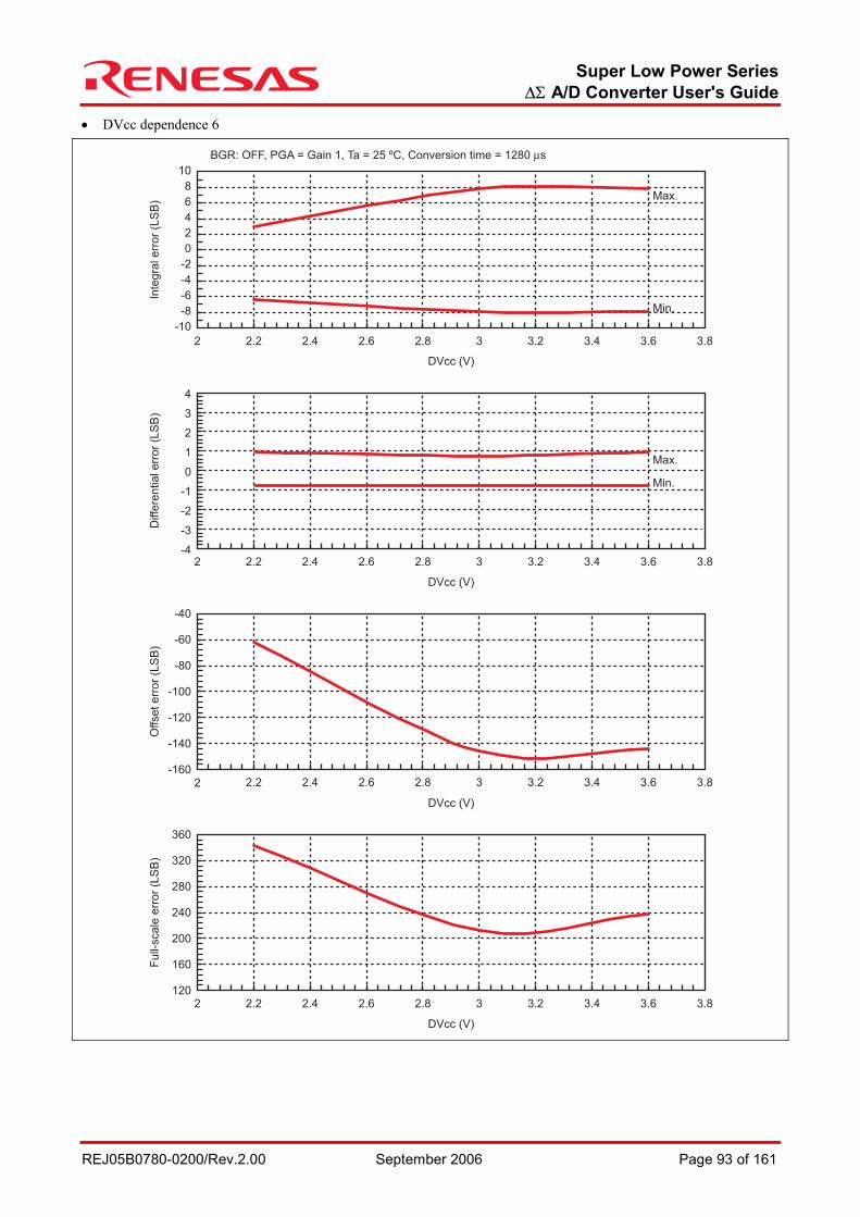
Super Low Power Series ∆Σ A/D Converter User's Guide
REJ05B0780-0200/Rev.2.00 September 2006 Page 93 of 161
• DVcc dependence 6
Inte
gra
l err
or
(LS
B)
Diffe
rential err
or
(LS
B)
Full-
scale
err
or
(LS
B)
Offset err
or
(LS
B)
Max.
Min.
Max.
Min.
-4
-3
-2
-1
0
1
2
3
4
DVcc (V)
2.62
-10
-4
0
4
8
-6
-2
2
6
10
-8
3.22.4 32.2 2.8
2
BGR: OFF, PGA = Gain 1, Ta = 25 ºC, Conversion time = 1280 µs
3.83.63.4
2.62 3.22.4 32.2 2.8 3.83.63.4
2.6 3.22.4 32.2 2.8 3.83.63.4
2.62 3.22.4 32.2 2.8 3.83.63.4
-80
-60
-40
-160
-120
-100
-140
280
320
360
120
200
240
160
DVcc (V)
DVcc (V)
DVcc (V)
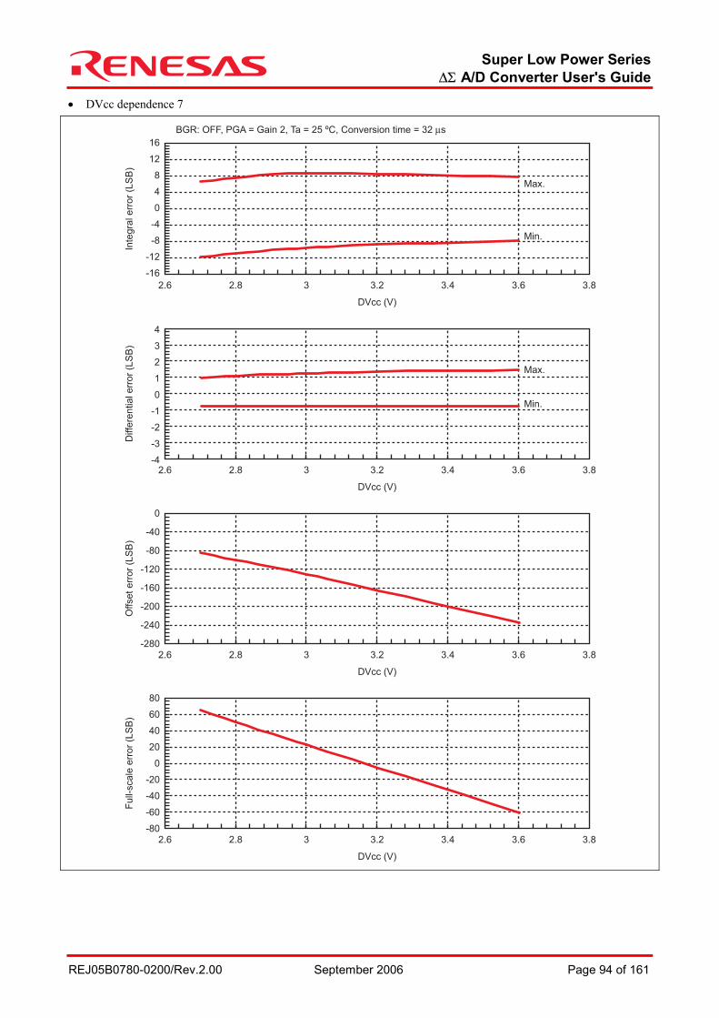
Super Low Power Series ∆Σ A/D Converter User's Guide
REJ05B0780-0200/Rev.2.00 September 2006 Page 94 of 161
• DVcc dependence 7
Inte
gra
l err
or
(LS
B)
Diffe
rential err
or
(LS
B)
Full-
scale
err
or
(LS
B)
Offset err
or
(LS
B)
Max.
Min.
Max.
Min.
3.22.6 3.83 3.62.8 3.4
3.22.6 3.83 3.62.8 3.4
3.22.6 3.83 3.62.8 3.4
3.22.6 3.83 3.62.8 3.4
-4
-3
-2
-1
0
1
2
3
4
DVcc (V)
-16
-4
4
12
-8
0
8
16
-12
BGR: OFF, PGA = Gain 2, Ta = 25 ºC, Conversion time = 32 µs
-80
-40
0
-280
-160
-120
-200
-240
0
40
80
20
60
-80
-40
-20
-60
DVcc (V)
DVcc (V)
DVcc (V)

Super Low Power Series ∆Σ A/D Converter User's Guide
REJ05B0780-0200/Rev.2.00 September 2006 Page 95 of 161
• DVcc dependence 8
Max.
Min.
Max.
Min.
-4
-3
-2
-1
0
1
2
3
4
DVcc (V)
2.62-20
0
-5
5
10
15
25
30
-10
20
-15
3.22.4 32.2 2.8
2.62 2.4 32.2 2.8
2.62 2.4 32.2 2.8
2.62 2.4 32.2 2.8
BGR: OFF, PGA = Gain 2, Ta = 25 ºC, Conversion time = 64 µs
40
200
160
120
80
280
240
-240
-40
0
-200
-120
-80
-160
DVcc (V)
3.2
DVcc (V)
3.2
Inte
gra
l err
or
(LS
B)
Diffe
rential err
or
(LS
B)
Full-
scale
err
or
(LS
B)
Offset err
or
(LS
B)
DVcc (V)
3.2
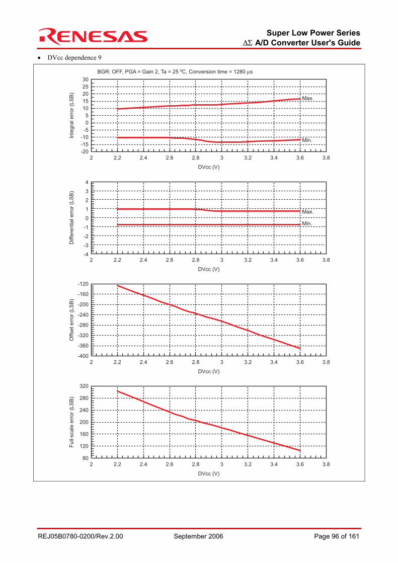
Super Low Power Series ∆Σ A/D Converter User's Guide
REJ05B0780-0200/Rev.2.00 September 2006 Page 96 of 161
• DVcc dependence 9
Inte
gra
l err
or
(LS
B)
Diffe
rential err
or
(LS
B)
Full-
scale
err
or
(LS
B)
Offset err
or
(LS
B)
DVcc (V)
DVcc (V)
DVcc (V)
DVcc (V)
Max.
Min.
Max.
Min.
-20
0
-5
5
10
15
25
30
-10
20
-15
2.62 3.22.4 32.2 2.8 3.83.63.4
2.62 3.22.4 32.2 2.8 3.83.63.4
2.62 3.22.4 32.2 2.8 3.83.63.4
2.62 3.22.4 32.2 2.8 3.83.63.4
-4
-3
-2
-1
0
1
2
3
4
BGR: OFF, PGA = Gain 2, Ta = 25 ºC, Conversion time = 1280 µs
80
240
200
160
120
320
280
-400
-160
-120
-320
-360
-240
-200
-280
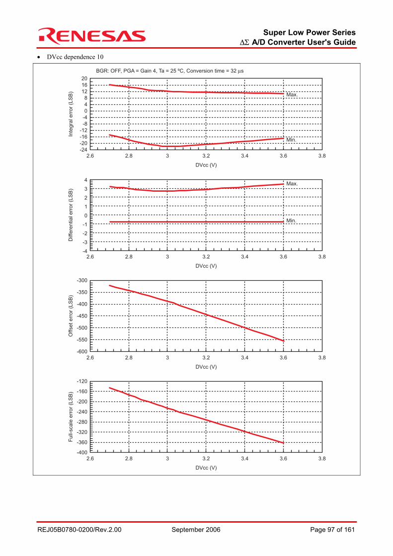
Super Low Power Series ∆Σ A/D Converter User's Guide
REJ05B0780-0200/Rev.2.00 September 2006 Page 97 of 161
• DVcc dependence 10
Inte
gra
l err
or
(LS
B)
Diffe
rential err
or
(LS
B)
Full-
scale
err
or
(LS
B)
Offset err
or
(LS
B)
DVcc (V)
DVcc (V)
DVcc (V)
DVcc (V)
Max.
Min.
Max.
Min.
3.22.6 3.83 3.62.8 3.4
3.22.6 3.83 3.62.8 3.4
3.22.6 3.83 3.62.8 3.4
3.22.6 3.83 3.62.8 3.4
-4
-3
-2
-1
0
1
2
3
4
-24
-8
-12
-4
0
4
12
16
20
-16
8
-20
BGR: OFF, PGA = Gain 4, Ta = 25 ºC, Conversion time = 32 µs
-400
-240
-280
-320
-360
-120
-200
-160
-600
-450
-500
-550
-300
-400
-350

Super Low Power Series ∆Σ A/D Converter User's Guide
REJ05B0780-0200/Rev.2.00 September 2006 Page 98 of 161
• DVcc dependence 11
Inte
gra
l err
or
(LS
B)
Diffe
rential err
or
(LS
B)
Full-
scale
err
or
(LS
B)
Offset err
or
(LS
B)
DVcc (V)
DVcc (V)
DVcc (V)
DVcc (V)
Max.
Min.
Max.
Min.
2.62 3.22.4 32.2 2.8
2.62 3.22.4 32.2 2.8
2.62 3.22.4 32.2 2.8
2.62 3.22.4 32.2 2.8
-4
-3
-2
-1
0
1
2
3
4
-30
-10
-15
-5
0
5
15
20
-20
10
-25
BGR: OFF, PGA = Gain 4, Ta = 25 ºC, Conversion time = 64 µs
-500
-340
-380
-300
-260
-220
-180
-420
-460
-160
0
-40
40
80
120
160
-80
-120
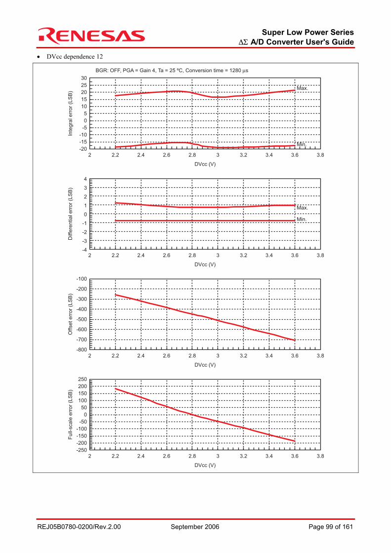
Super Low Power Series ∆Σ A/D Converter User's Guide
REJ05B0780-0200/Rev.2.00 September 2006 Page 99 of 161
• DVcc dependence 12
Inte
gra
l err
or
(LS
B)
Diffe
rential err
or
(LS
B)
Full-
scale
err
or
(LS
B)
Offset err
or
(LS
B)
DVcc (V)
DVcc (V)
DVcc (V)
DVcc (V)
Max.
Min.
Max.
Min.
-20
0
-5
5
10
15
25
30
-10
20
-15
2.62 3.22.4 32.2 2.8 3.83.63.4
2.62 3.22.4 32.2 2.8 3.83.63.4
2.62 3.22.4 32.2 2.8 3.83.63.4
2.62 3.22.4 32.2 2.8 3.83.63.4
-4
-3
-2
-1
0
1
2
3
4
BGR: OFF, PGA = Gain 4, Ta = 25 ºC, Conversion time = 1280 µs
-250
50
-50
-150
-200
250
150
0
-100
200
100
-800
-200
-100
-600
-700
-400
-300
-500
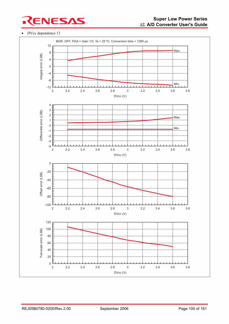
Super Low Power Series ∆Σ A/D Converter User's Guide
REJ05B0780-0200/Rev.2.00 September 2006 Page 100 of 161
• DVcc dependence 13
Inte
gra
l err
or
(LS
B)
Diffe
rential err
or
(LS
B)
Full-
scale
err
or
(LS
B)
Offset err
or
(LS
B)
DVcc (V)
DVcc (V)
DVcc (V)
DVcc (V)
Max.
Min.
Max.
Min.
2.62 3.22.4 32.2 2.8 3.83.63.4
2.62 3.22.4 32.2 2.8 3.83.63.4
2.62 3.22.4 32.2 2.8 3.83.63.4
2.62 3.22.4 32.2 2.8 3.83.63.4
-4
-3
-2
-1
0
1
2
3
4
BGR: OFF, PGA = Gain 1/3, Ta = 25 ºC, Conversion time = 1280 µs
0
80
60
40
20
120
100
-12
4
0
-4
-8
12
8
-100
-20
-40
-60
-80
0

Super Low Power Series ∆Σ A/D Converter User's Guide
REJ05B0780-0200/Rev.2.00 September 2006 Page 101 of 161
(4) Dependences on PGA Setting
• PGA dependence 1
Gain 1Gain 1/3 Gain 4Bypass Gain 2
PGA
Gain 1Gain 1/3 Gain 4Bypass Gain 2
PGA
Gain 1Gain 1/3 Gain 4Bypass Gain 2
PGA
Gain 1Gain 1/3 Gain 4Bypass Gain 2
PGA
Inte
gra
l err
or
(LS
B)
Diffe
rential err
or
(LS
B)
Full-
scale
err
or
(LS
B)
Offset err
or
(LS
B)
Max.
Min.
Max.
Min.
-4
-3
-2
-1
0
1
2
3
4
BGR: OFF, Vcc = DVcc = 2.2 V, Vref = 1.98 V, Ta = 25 ºC, Conversion time = 64 µs
80
240
200
160
120
320
280
-25
0
-10
-15
-20
20
10
-5
15
5
-300
300
100
200
0
-100
-200
400
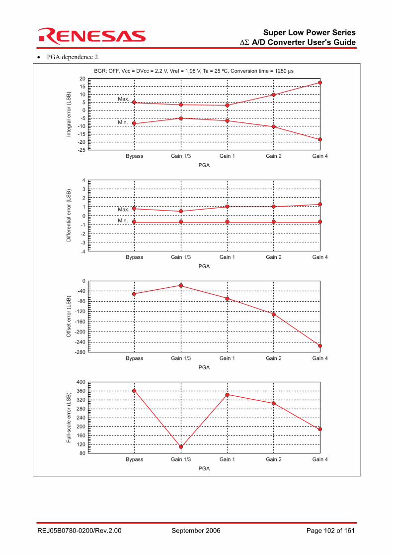
Super Low Power Series ∆Σ A/D Converter User's Guide
REJ05B0780-0200/Rev.2.00 September 2006 Page 102 of 161
• PGA dependence 2
Gain 1Gain 1/3 Gain 4Bypass Gain 2
PGA
Gain 1Gain 1/3 Gain 4Bypass Gain 2
PGA
Gain 1Gain 1/3 Gain 4Bypass Gain 2
PGA
Gain 1Gain 1/3 Gain 4Bypass Gain 2
PGA
Inte
gra
l err
or
(LS
B)
Diffe
rential err
or
(LS
B)
Full-
scale
err
or
(LS
B)
Offset err
or
(LS
B)
Max.
Min.
Max.
Min.
-4
-3
-2
-1
0
1
2
3
4
BGR: OFF, Vcc = DVcc = 2.2 V, Vref = 1.98 V, Ta = 25 ºC, Conversion time = 1280 µs
80
240
200
160
120
400
320
360
280
-25
0
-10
-15
-20
20
10
-5
15
5
-280
-40
-120
-80
-160
-200
-240
0
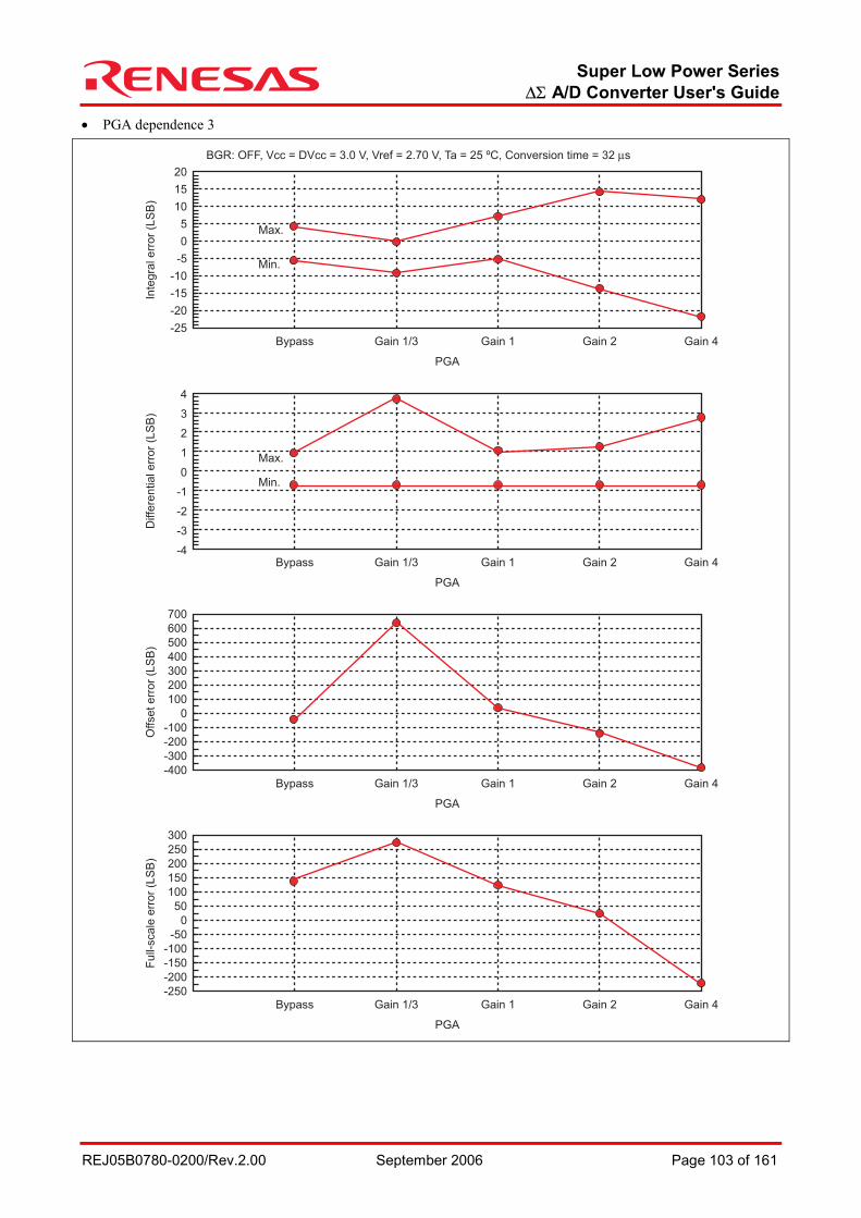
Super Low Power Series ∆Σ A/D Converter User's Guide
REJ05B0780-0200/Rev.2.00 September 2006 Page 103 of 161
• PGA dependence 3
Gain 1Gain 1/3 Gain 4Bypass Gain 2
PGA
Gain 1Gain 1/3 Gain 4Bypass Gain 2
PGA
Gain 1Gain 1/3 Gain 4Bypass Gain 2
PGA
Gain 1Gain 1/3 Gain 4Bypass Gain 2
PGA
Inte
gra
l err
or
(LS
B)
Diffe
rential err
or
(LS
B)
Full-
scale
err
or
(LS
B)
Offset err
or
(LS
B)
Max.
Min.
Max.
Min.
-4
-3
-2
-1
0
1
2
3
4
BGR: OFF, Vcc = DVcc = 3.0 V, Vref = 2.70 V, Ta = 25 ºC, Conversion time = 32 µs
-25
0
-10
-15
-20
20
10
-5
15
5
-400
500
100
300
-100
-200
-300
700
400
0
200
600
-250
200
0
100
-100
-150
-200
300
150
-50
50
250
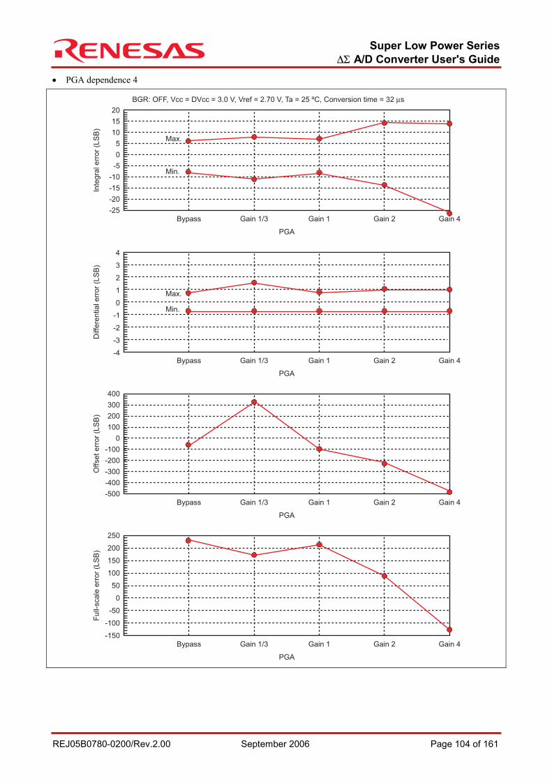
Super Low Power Series ∆Σ A/D Converter User's Guide
REJ05B0780-0200/Rev.2.00 September 2006 Page 104 of 161
• PGA dependence 4
Gain 1Gain 1/3 Gain 4Bypass Gain 2
PGA
Gain 1Gain 1/3 Gain 4Bypass Gain 2
PGA
Gain 1Gain 1/3 Gain 4Bypass Gain 2
PGA
Gain 1Gain 1/3 Gain 4Bypass Gain 2
PGA
Inte
gra
l err
or
(LS
B)
Diffe
rential err
or
(LS
B)
Full-
scale
err
or
(LS
B)
Offset err
or
(LS
B)
Max.
Min.
Max.
Min.
-4
-3
-2
-1
0
1
2
3
4
BGR: OFF, Vcc = DVcc = 3.0 V, Vref = 2.70 V, Ta = 25 ºC, Conversion time = 32 µs
-25
0
-10
-15
-20
20
10
-5
15
5
-500
0
200
-100
-300
-200
-400
400
300
100
-150
100
200
50
-50
0
-100
250
150
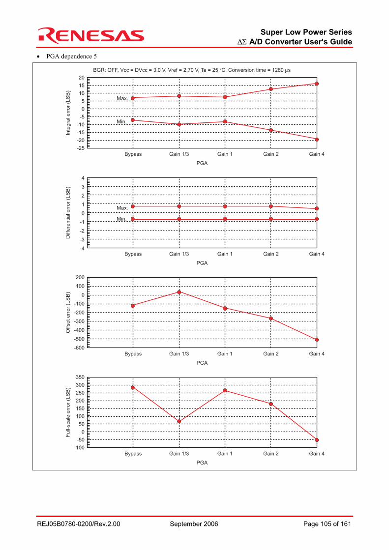
Super Low Power Series ∆Σ A/D Converter User's Guide
REJ05B0780-0200/Rev.2.00 September 2006 Page 105 of 161
• PGA dependence 5
Max.
Min.
Max.
Min.
Inte
gra
l err
or
(LS
B)
Diffe
rential err
or
(LS
B)
Full-
scale
err
or
(LS
B)
Offset err
or
(LS
B)
Gain 1Gain 1/3 Gain 4Bypass Gain 2
-4
-3
-2
-1
0
1
2
3
4
PGA
BGR: OFF, Vcc = DVcc = 3.0 V, Vref = 2.70 V, Ta = 25 ºC, Conversion time = 1280 µs
Gain 1Gain 1/3 Gain 4Bypass Gain 2
PGA
Gain 1Gain 1/3 Gain 4Bypass Gain 2
PGA
Gain 1Gain 1/3 Gain 4Bypass Gain 2
PGA
-25
0
-10
-15
-20
20
10
-5
15
5
-100
150
250
100
0
50
-50
350
300
200
-600
-100
100
-200
-400
-300
-500
200
0
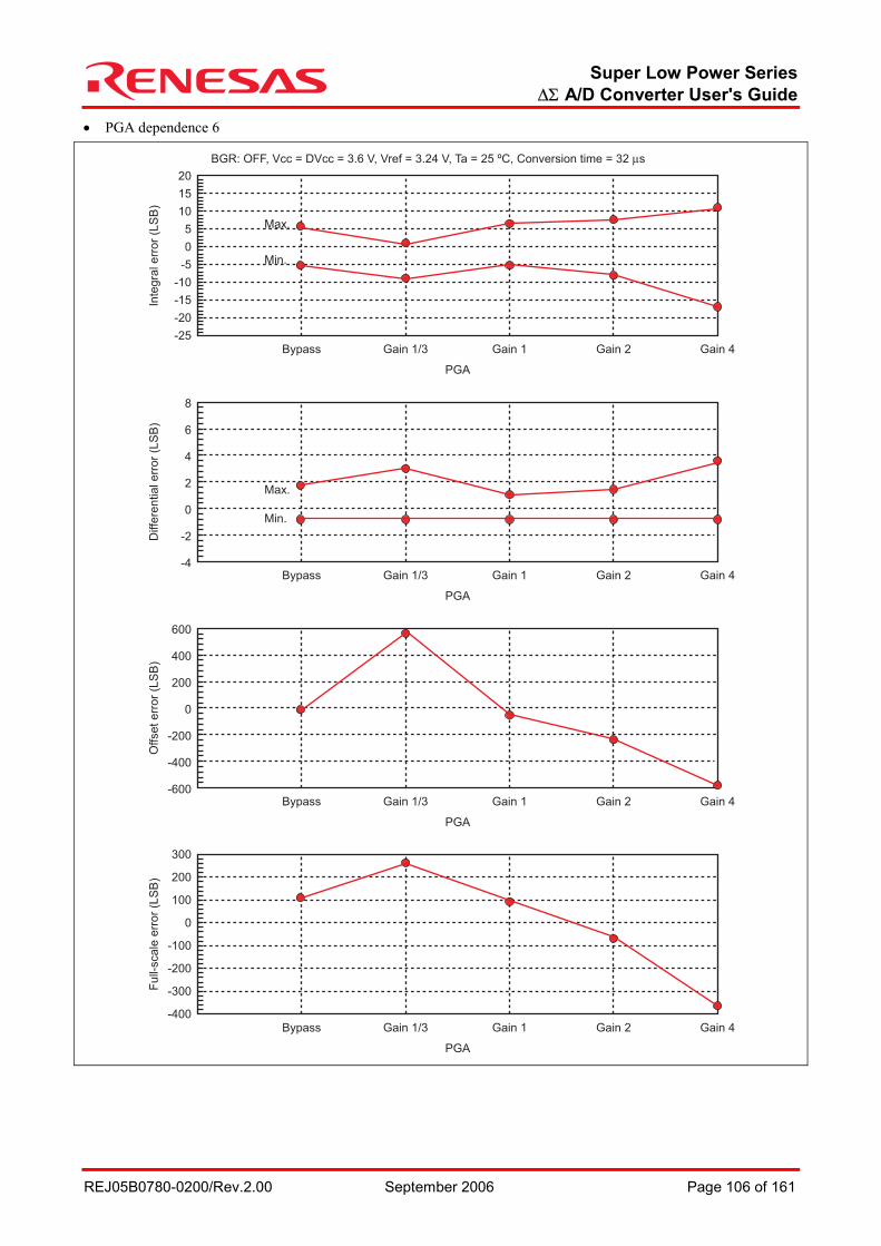
Super Low Power Series ∆Σ A/D Converter User's Guide
REJ05B0780-0200/Rev.2.00 September 2006 Page 106 of 161
• PGA dependence 6
Gain 1Gain 1/3 Gain 4Bypass Gain 2
PGA
Gain 1Gain 1/3 Gain 4Bypass Gain 2
PGA
Gain 1Gain 1/3 Gain 4Bypass Gain 2
PGA
Gain 1Gain 1/3 Gain 4Bypass Gain 2
PGA
Inte
gra
l err
or
(LS
B)
Diffe
rential err
or
(LS
B)
Full-
scale
err
or
(LS
B)
Offset err
or
(LS
B)
Max.
Min.
Max.
Min.
-4
-2
0
2
4
6
8
BGR: OFF, Vcc = DVcc = 3.6 V, Vref = 3.24 V, Ta = 25 ºC, Conversion time = 32 µs
-600
-400
-200
0
200
400
600
-25
0
-10
-15
-20
20
10
-5
15
5
-400
100
0
-200
-100
-300
300
200

Super Low Power Series ∆Σ A/D Converter User's Guide
REJ05B0780-0200/Rev.2.00 September 2006 Page 107 of 161
• PGA dependence 7
Gain 1Gain 1/3 Gain 4Bypass Gain 2
PGA
Gain 1Gain 1/3 Gain 4Bypass Gain 2
PGA
Gain 1Gain 1/3 Gain 4Bypass Gain 2
PGA
Gain 1Gain 1/3 Gain 4Bypass Gain 2
PGA
Inte
gra
l err
or
(LS
B)
Diffe
rential err
or
(LS
B)
Full-
scale
err
or
(LS
B)
Offset err
or
(LS
B)
Max.
Min.
Max.
Min.
-4
-3
-2
-1
0
1
2
3
4
BGR: OFF, Vcc = DVcc = 3.6 V, Vref = 3.24 V, Ta = 25 ºC, Conversion time = 1280 µs
25
0
-10
-15
-20
20
10
-5
15
5
-300
200
100
-200
-100
400
300
-800
-300
-400
-600
-500
-700
0
-100
-200
Super Low Power Series ∆Σ A/D Converter User's Guide
REJ05B0780-0200/Rev.2.00 September 2006 Page 108 of 161
7.1.2 Mask ROM Version Graphs of the dependences of the integral error, differential error, offset error and full-scale error on the parameters listed in the table below are given after the table.
Table 7.2 Conditions in Parameter-Dependence Measurement (MASK ROM Version)
Measurement Conditions
Graph Name BGR Vcc (V) DVcc (V) Vref (V) Ta (°C) PGA Conversion Time (µs)
Conversion time dependence 1 OFF 2.2 2.2 1.98 25 Bypassed Conversion time dependence 2 OFF 3.0 3.0 2.70 25 Bypassed Conversion time dependence 3 OFF 2.2 2.2 1.98 25 1 Conversion time dependence 4 OFF 3.0 3.0 2.70 25 1 Conversion time dependence 5 OFF 3.6 3.6 3.24 25 1 Conversion time dependence 6 OFF 2.2 2.2 1.98 25 2 Conversion time dependence 7 OFF 3.0 3.0 2.70 25 2 Conversion time dependence 8 OFF 2.2 2.2 1.98 25 4 Conversion time dependence 9 OFF 3.0 3.0 2.70 25 4 Conversion time dependence 10 OFF 2.2 2.2 1.98 25 1/3 Conversion time dependence 11 OFF 3.0 3.0 2.70 25 1/3 Conversion time dependence 12 ON 2.2 2.2 25 Bypassed Conversion time dependence 13 ON 3.0 3.0 25 Bypassed Conversion time dependence 14 ON 2.2 2.2 25 1 Conversion time dependence 15 ON 3.0 3.0 25 1 Conversion time dependence 16 ON 2.2 2.2 25 1/3 Conversion time dependence 17 ON 3.0 3.0 25 1/3 Temperature dependence 1 OFF 2.2 2.2 Bypassed 64 Temperature dependence 2 OFF 3.0 3.0 Bypassed 32 Temperature dependence 3 OFF 3.0 3.0 Bypassed 64 Temperature dependence 4 OFF 2.2 2.2 1 64 Temperature dependence 5 OFF 3.0 3.0 1 32 Temperature dependence 6 OFF 3.0 3.0 1 64 Temperature dependence 7 OFF 3.0 3.0 2 32 Temperature dependence 8 OFF 3.0 3.0 2 64 Temperature dependence 9 OFF 3.0 3.0 4 32 Temperature dependence 10 OFF 3.0 3.0 4 64 Temperature dependence 11 OFF 3.0 3.0 1/3 32 Temperature dependence 12 OFF 3.0 3.0 1/3 64 DVcc dependence 1 OFF 25 Bypassed 64 DVcc dependence 2 OFF 25 1 64 DVcc dependence 3 OFF 25 2 64 DVcc dependence 4 OFF 25 4 64 DVcc dependence 5 OFF 25 1/3 64 DVcc dependence 6 ON 25 Bypassed 64 DVcc dependence 7 ON 25 1 64 DVcc dependence 8 ON 25 1/3 64 PGA dependence 1 OFF 2.2 2.2 1.98 25 64 PGA dependence 2 OFF 3.0 3.0 1.98 25 32
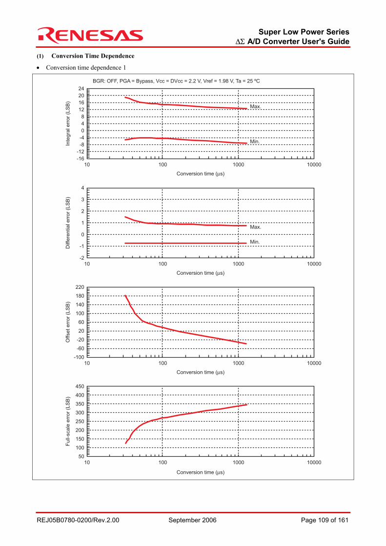
Super Low Power Series ∆Σ A/D Converter User's Guide
REJ05B0780-0200/Rev.2.00 September 2006 Page 109 of 161
(1) Conversion Time Dependence
• Conversion time dependence 1 In
tegra
l err
or
(LS
B)
Conversion time (µs)
Diffe
ren
tia
l e
rro
r (L
SB
)
Conversion time (µs)
Offset err
or
(LS
B)
Conversion time (µs)
Fu
ll-sca
le e
rro
r (L
SB
)
Conversion time (µs)
10010-16
-12
-8
-4
0
4
8
16
24
12
20
1000 10000
BGR: OFF, PGA = Bypass, Vcc = DVcc = 2.2 V, Vref = 1.98 V, Ta = 25 ºC
Max.
Min.
Max.
Min.
10010-2
-1
0
1
2
3
4
1000 10000
10010-100
-20
-60
20
60
140
220
100
180
1000 10000
10010 1000 1000050
150
100
200
250
350
450
300
400
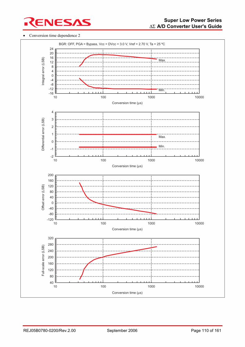
Super Low Power Series ∆Σ A/D Converter User's Guide
REJ05B0780-0200/Rev.2.00 September 2006 Page 110 of 161
• Conversion time dependence 2
Inte
gra
l err
or
(LS
B)
Conversion time (µs)
Diffe
ren
tia
l e
rro
r (L
SB
)
Conversion time (µs)
Offset err
or
(LS
B)
Conversion time (µs)
Fu
ll-sca
le e
rro
r (L
SB
)
Conversion time (µs)
Max.
Min.
Max.
Min.
10010-16
-12
-8
-4
0
4
8
16
24
12
20
1000 10000
BGR: OFF, PGA = Bypass, Vcc = DVcc = 3.0 V, Vref = 2.70 V, Ta = 25 ºC
10010-2
-1
0
1
2
3
4
1000 10000
10010-120
-40
-80
0
40
120
200
80
160
1000 10000
10010 1000 1000040
80
120
160
240
320
200
280
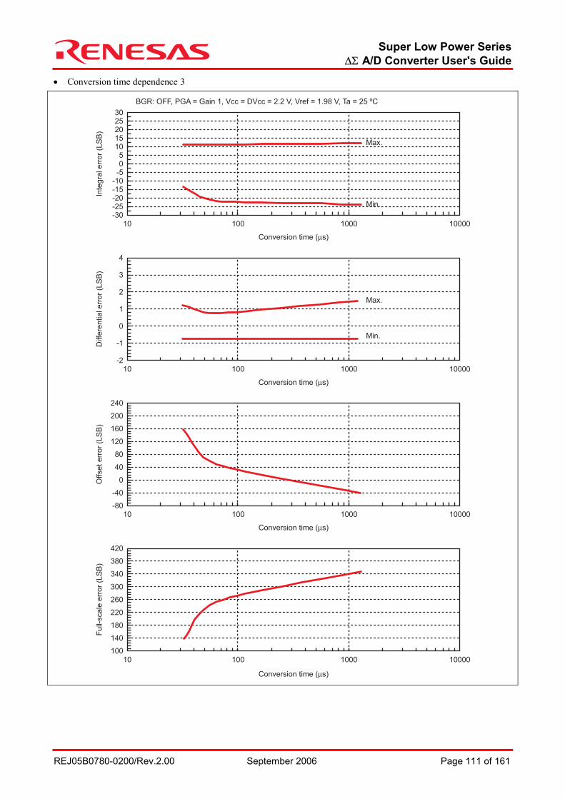
Super Low Power Series ∆Σ A/D Converter User's Guide
REJ05B0780-0200/Rev.2.00 September 2006 Page 111 of 161
• Conversion time dependence 3
Inte
gra
l err
or
(LS
B)
Conversion time (µs)
Diffe
ren
tia
l e
rro
r (L
SB
)
Conversion time (µs)
Offset err
or
(LS
B)
Conversion time (µs)
Fu
ll-sca
le e
rro
r (L
SB
)
Conversion time (µs)
Max.
Min.
Max.
Min.
10010-30-25-20-15-10
-50
10
30
5
2025
15
1000 10000
BGR: OFF, PGA = Gain 1, Vcc = DVcc = 2.2 V, Vref = 1.98 V, Ta = 25 ºC
10010-2
-1
0
1
2
3
4
1000 10000
10010-80
0
-40
40
80
160
240
120
200
1000 10000
10010 1000 10000100
180
140
220
260
340
420
300
380
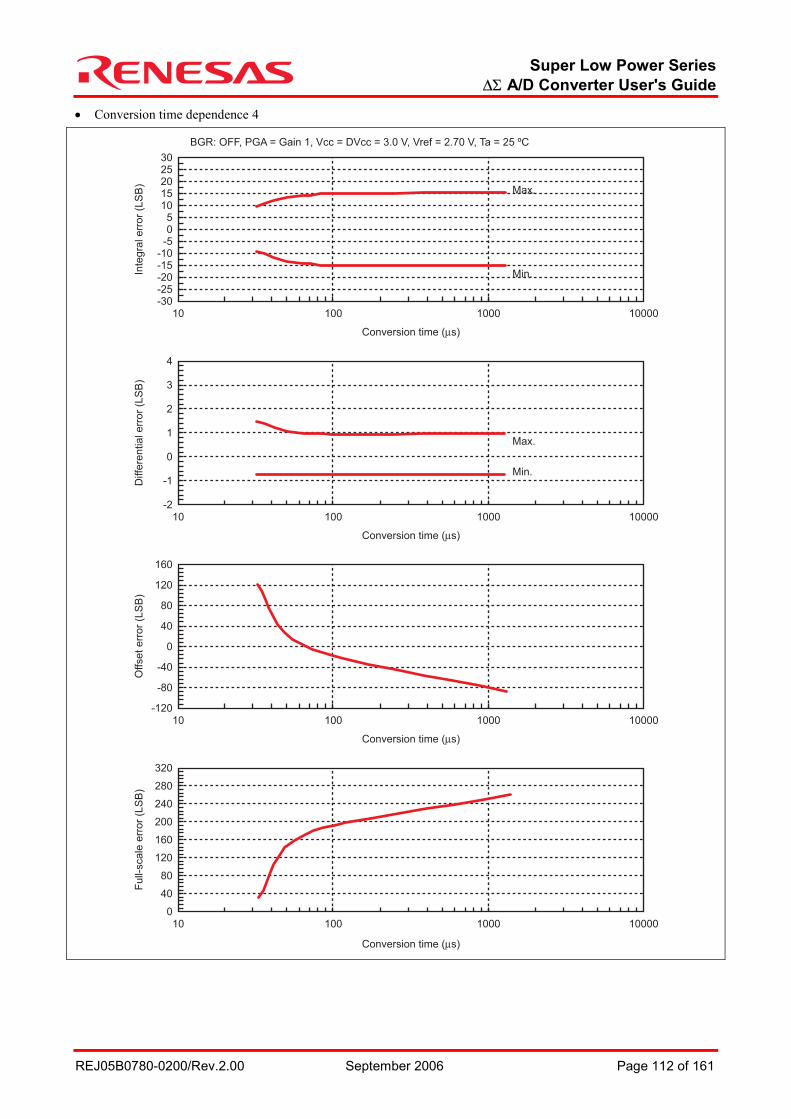
Super Low Power Series ∆Σ A/D Converter User's Guide
REJ05B0780-0200/Rev.2.00 September 2006 Page 112 of 161
• Conversion time dependence 4
Inte
gra
l err
or
(LS
B)
Conversion time (µs)
Diffe
ren
tia
l e
rro
r (L
SB
)
Conversion time (µs)
Offset err
or
(LS
B)
Conversion time (µs)
Fu
ll-sca
le e
rro
r (L
SB
)
Conversion time (µs)
Max.
Min.
Max.
Min.
10010-30-25-20-15-10
-50
10
30
5
2025
15
1000 10000
BGR: OFF, PGA = Gain 1, Vcc = DVcc = 3.0 V, Vref = 2.70 V, Ta = 25 ºC
.
10010-2
-1
0
1
2
3
4
1000 10000
10010-120
-40
-80
0
40
120
160
80
1000 10000
10010 1000 100000
80
40
120
160
240
320
200
280
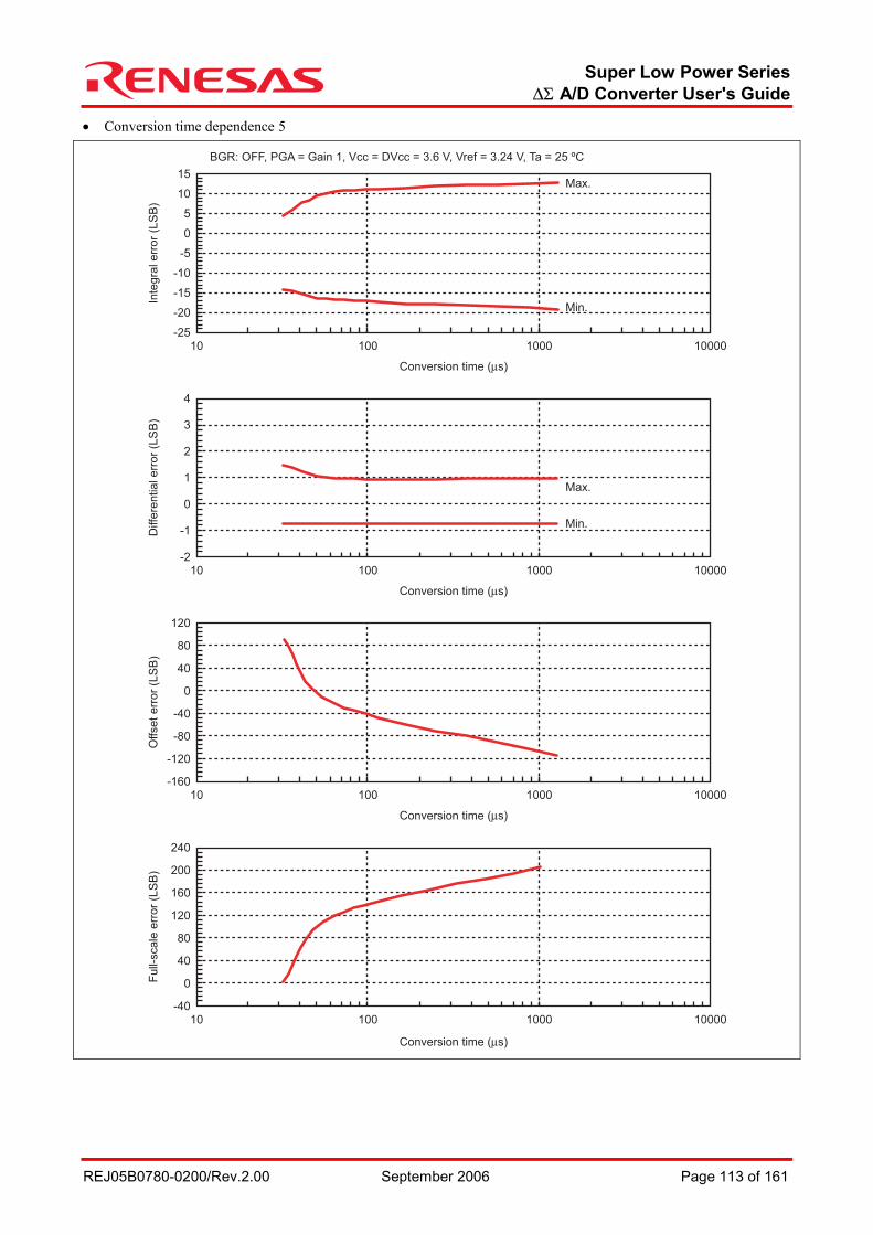
Super Low Power Series ∆Σ A/D Converter User's Guide
REJ05B0780-0200/Rev.2.00 September 2006 Page 113 of 161
• Conversion time dependence 5
Inte
gra
l err
or
(LS
B)
Conversion time (µs)
Diffe
ren
tia
l e
rro
r (L
SB
)
Conversion time (µs)
Offset err
or
(LS
B)
Conversion time (µs)
Fu
ll-sca
le e
rro
r (L
SB
)
Conversion time (µs)
Max.
Min.
Max.
Min.
10010 1000 10000
BGR: OFF, PGA = Gain 1, Vcc = DVcc = 3.6 V, Vref = 3.24 V, Ta = 25 ºC
10010-2
-1
0
1
2
3
4
1000 10000
10010-160
-120
-40
-80
0
40
120
80
1000 10000
10010 1000 10000-40
0
80
40
120
160
240
200
-25
-20
-10
-15
-5
0
10
15
5
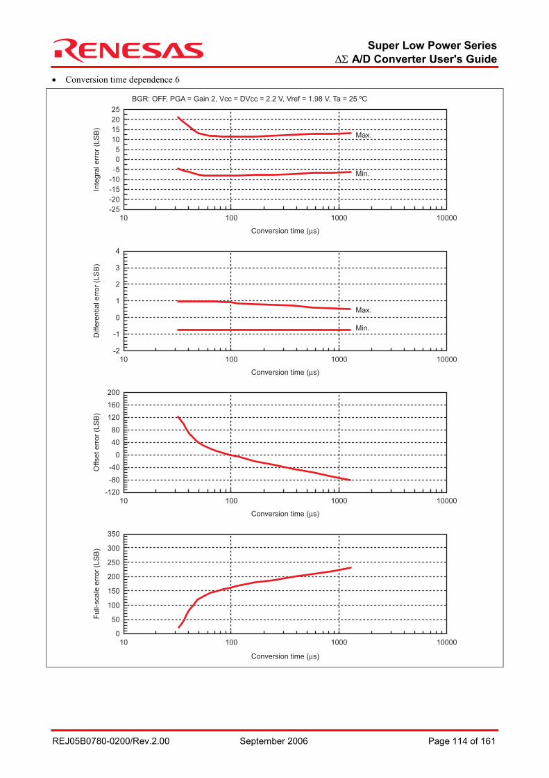
Super Low Power Series ∆Σ A/D Converter User's Guide
REJ05B0780-0200/Rev.2.00 September 2006 Page 114 of 161
• Conversion time dependence 6
Inte
gra
l err
or
(LS
B)
Conversion time (µs)
Diffe
ren
tia
l e
rro
r (L
SB
)
Conversion time (µs)
Offset err
or
(LS
B)
Conversion time (µs)
Fu
ll-sca
le e
rro
r (L
SB
)
Conversion time (µs)
Max.
Min.
Max.
Min.
10010-25
-20
-15
-10
-5
0
10
25
5
20
15
1000 10000
BGR: OFF, PGA = Gain 2, Vcc = DVcc = 2.2 V, Vref = 1.98 V, Ta = 25 ºC
10010-2
-1
0
1
2
3
4
1000 10000
10010-120
-80
0
-40
40
80
160
200
120
1000 10000
10010 1000 100000
50
100
150
250
350
200
300
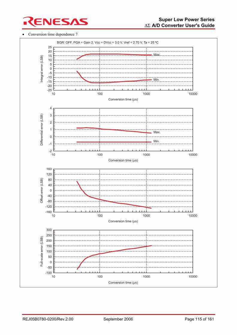
Super Low Power Series ∆Σ A/D Converter User's Guide
REJ05B0780-0200/Rev.2.00 September 2006 Page 115 of 161
• Conversion time dependence 7
Inte
gra
l err
or
(LS
B)
Conversion time (µs)
Diffe
ren
tia
l e
rro
r (L
SB
)
Conversion time (µs)
Offset err
or
(LS
B)
Conversion time (µs)
Fu
ll-sca
le e
rro
r (L
SB
)
Conversion time (µs)
Max.
Min.
Max.
Min.
10010-25
-20
-15
-10
-5
0
10
25
5
20
15
1000 10000
BGR: OFF, PGA = Gain 2, Vcc = DVcc = 3.0 V, Vref = 2.70 V, Ta = 25 ºC
10010-2
-1
0
1
2
3
4
1000 10000
10010-160
-120
-40
-80
0
40
120
160
80
1000 10000
10010 1000 10000-100
0
-50
50
100
200
300
150
250

Super Low Power Series ∆Σ A/D Converter User's Guide
REJ05B0780-0200/Rev.2.00 September 2006 Page 116 of 161
• Conversion time dependence 8
Inte
gra
l err
or
(LS
B)
Conversion time (µs)
Diffe
ren
tia
l e
rro
r (L
SB
)
Conversion time (µs)
Offset err
or
(LS
B)
Conversion time (µs)
Fu
ll-sca
le e
rro
r (L
SB
)
Conversion time (µs)
10010-25
-20
-15
-10
-5
0
10
25
5
20
15
1000 10000
BGR: OFF, PGA = Gain 4, Vcc = DVcc = 2.2 V, Vref = 1.98 V, Ta = 25 ºC
10010-2
-1
0
1
2
3
4
1000 10000
10010-200
-160
-80
-120
-40
0
80
120
40
1000 10000
10010 1000 10000-100
0
-50
50
100
200
250
150
Max.
Min.
Max.
Min.

Super Low Power Series ∆Σ A/D Converter User's Guide
REJ05B0780-0200/Rev.2.00 September 2006 Page 117 of 161
• Conversion time dependence 9
Inte
gra
l err
or
(LS
B)
Conversion time (µs)
Diffe
ren
tia
l e
rro
r (L
SB
)
Conversion time (µs)
Offset err
or
(LS
B)
Conversion time (µs)
Fu
ll-sca
le e
rro
r (L
SB
)
Conversion time (µs)
Max.
Min.
Max.
Min.
10010-25
-20
-15
-10
-5
0
10
25
5
20
15
1000 10000
BGR: OFF, PGA = Gain 4, Vcc = DVcc = 3.0 V, Vref = 2.70 V, Ta = 25 ºC
-300
-250
-200
-150
-100
-50
50
200
0
150
100
10010-2
-1
0
1
2
3
4
1000 10000
10010-280
-240
-200
-120
-160
-80
0
40
0
80
-40
1000 10000
10010 1000 10000

Super Low Power Series ∆Σ A/D Converter User's Guide
REJ05B0780-0200/Rev.2.00 September 2006 Page 118 of 161
• Conversion time dependence 10
Inte
gra
l err
or
(LS
B)
Conversion time (µs)
Diffe
ren
tia
l e
rro
r (L
SB
)
Conversion time (µs)
Offset err
or
(LS
B)
Conversion time (µs)
Fu
ll-sca
le e
rro
r (L
SB
)
Conversion time (µs)
Max.
Min.
Max.
Min.
10010-25
-20
-15
-10
-5
0
10
25
5
20
15
1000 10000
BGR: OFF, PGA = Gain 1/3, Vcc = DVcc = 2.2 V, Vref = 1.98 V, Ta = 25 ºC
0
100
200
300
400
500
700
1000
600
900
800
10010-2
-1
0
1
2
3
4
1000 10000
10010
100
150
200
250
300
400
450
500
350
1000 10000
10010 1000 10000
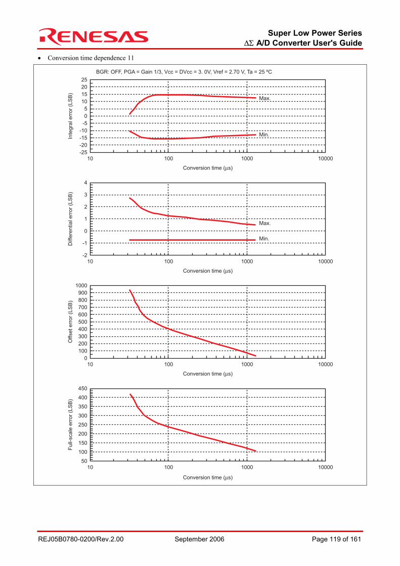
Super Low Power Series ∆Σ A/D Converter User's Guide
REJ05B0780-0200/Rev.2.00 September 2006 Page 119 of 161
• Conversion time dependence 11
Inte
gra
l err
or
(LS
B)
Conversion time (µs)
Diffe
ren
tia
l e
rro
r (L
SB
)
Conversion time (µs)
Offset err
or
(LS
B)
Conversion time (µs)
Fu
ll-sca
le e
rro
r (L
SB
)
Conversion time (µs)
Max.
Min.
Max.
Min.
10010-25
-20
-15
-10
-5
0
10
25
5
20
15
1000 10000
BGR: OFF, PGA = Gain 1/3, Vcc = DVcc = 3. 0V, Vref = 2.70 V, Ta = 25 ºC
0
100
200
300
400
500
700
1000
600
900
800
10010-2
-1
0
1
2
3
4
1000 10000
10010
50
100
150
200
250
300
400
450
350
1000 10000
10010 1000 10000
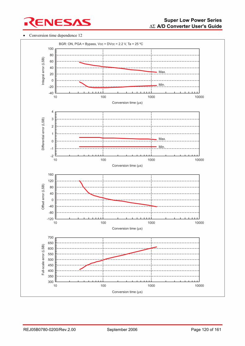
Super Low Power Series ∆Σ A/D Converter User's Guide
REJ05B0780-0200/Rev.2.00 September 2006 Page 120 of 161
• Conversion time dependence 12
Inte
gra
l err
or
(LS
B)
Conversion time (µs)
Diffe
ren
tia
l e
rro
r (L
SB
)
Conversion time (µs)
Offset err
or
(LS
B)
Conversion time (µs)
Fu
ll-sca
le e
rro
r (L
SB
)
Conversion time (µs)
Max.
Min.
Max.
Min.
10010 1000 10000
BGR: ON, PGA = Bypass, Vcc = DVcc = 2.2 V, Ta = 25 ºC
10010-2
-1
0
1
2
3
4
1000 10000
10010
300
350
400
450
500
550
650
700
600
1000 10000
10010 1000 10000
-40
-20
0
20
40
60
100
80
-120
-80
-40
0
40
80
160
120
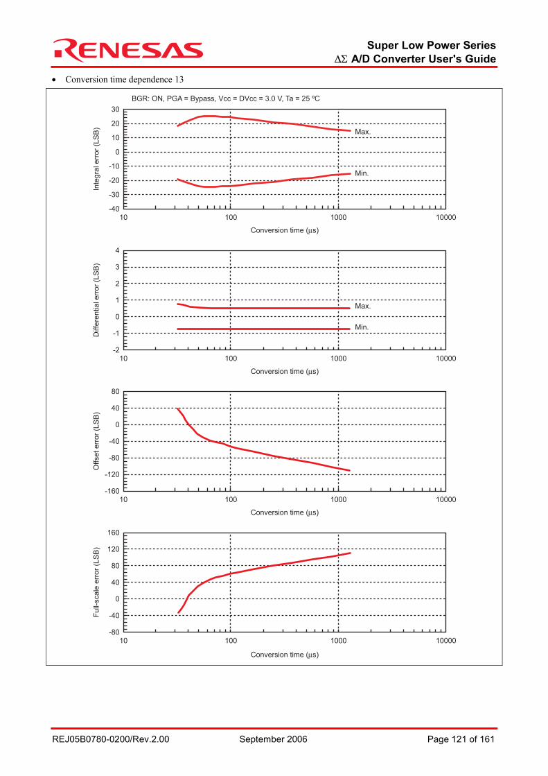
Super Low Power Series ∆Σ A/D Converter User's Guide
REJ05B0780-0200/Rev.2.00 September 2006 Page 121 of 161
• Conversion time dependence 13
Inte
gra
l err
or
(LS
B)
Conversion time (µs)
Diffe
ren
tia
l e
rro
r (L
SB
)
Conversion time (µs)
Offset err
or
(LS
B)
Conversion time (µs)
Fu
ll-sca
le e
rro
r (L
SB
)
Conversion time (µs)
Max.
Min.
Max.
Min.
10010 1000 10000
BGR: ON, PGA = Bypass, Vcc = DVcc = 3.0 V, Ta = 25 ºC
10010-2
-1
0
1
2
3
4
1000 10000
10010 1000 10000
10010 1000 10000
-40
-30
-20
-10
0
10
30
20
-160
-120
-80
-40
0
40
80
-80
-40
0
40
80
120
160
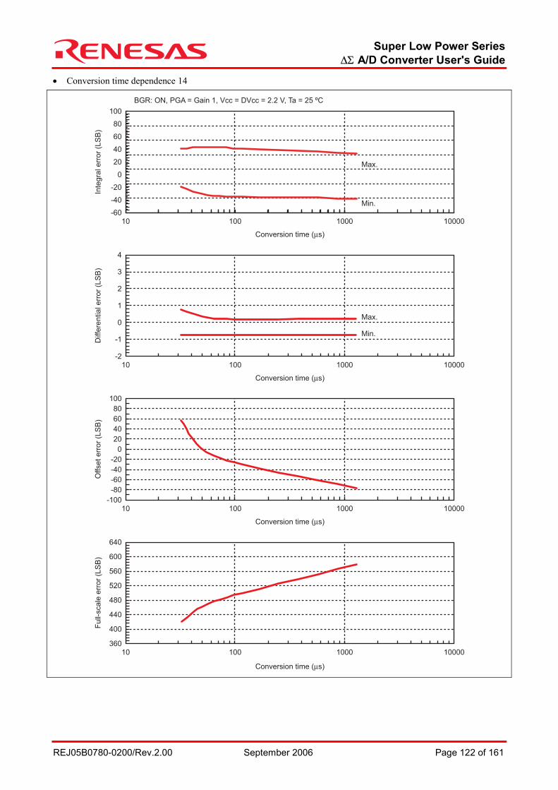
Super Low Power Series ∆Σ A/D Converter User's Guide
REJ05B0780-0200/Rev.2.00 September 2006 Page 122 of 161
• Conversion time dependence 14
Inte
gra
l err
or
(LS
B)
Conversion time (µs)
Diffe
ren
tia
l e
rro
r (L
SB
)
Conversion time (µs)
Offset err
or
(LS
B)
Conversion time (µs)
Fu
ll-sca
le e
rro
r (L
SB
)
Conversion time (µs)
Max.
Min.
Max.
Min.
-60
-40
-20
0
40
100
20
80
60
-100
-80
-60
-40
-20
0
40
100
20
80
60
10010 1000 10000
BGR: ON, PGA = Gain 1, Vcc = DVcc = 2.2 V, Ta = 25 ºC
10010-2
-1
0
1
2
3
4
1000 10000
10010 1000 10000
10010 1000 10000360
400
440
480
520
600
560
640
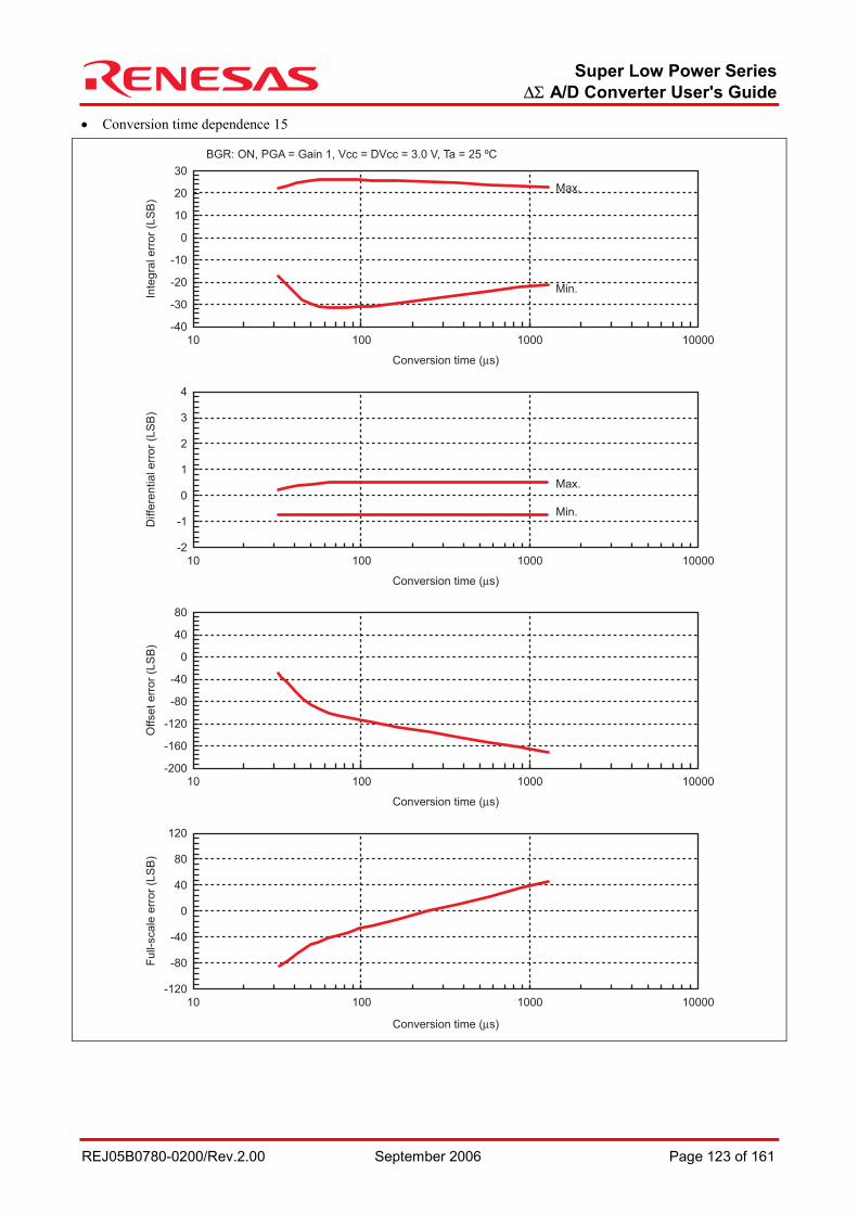
Super Low Power Series ∆Σ A/D Converter User's Guide
REJ05B0780-0200/Rev.2.00 September 2006 Page 123 of 161
• Conversion time dependence 15
Inte
gra
l err
or
(LS
B)
Conversion time (µs)
Diffe
ren
tia
l e
rro
r (L
SB
)
Conversion time (µs)
Offset err
or
(LS
B)
Conversion time (µs)
Fu
ll-sca
le e
rro
r (L
SB
)
Conversion time (µs)
Max.
Min.
Max.
Min.
10
10-2
-1
0
1
2
3
4
10
10
-40
-30
-20
-10
0
10
30
20 .
-200
-160
-120
-80
-40
0
40
80
-120
-80
-40
0
40
80
120
100 1000 10000
BGR: ON, PGA = Gain 1, Vcc = DVcc = 3.0 V, Ta = 25 ºC
100 1000 10000
100 1000 10000
100 1000 10000
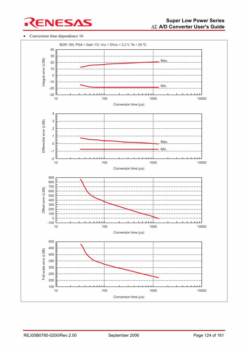
Super Low Power Series ∆Σ A/D Converter User's Guide
REJ05B0780-0200/Rev.2.00 September 2006 Page 124 of 161
• Conversion time dependence 16
Inte
gra
l err
or
(LS
B)
Conversion time (µs)
Diffe
ren
tia
l e
rro
r (L
SB
)
Conversion time (µs)
Offset err
or
(LS
B)
Conversion time (µs)
Fu
ll-sca
le e
rro
r (L
SB
)
Conversion time (µs)
10
10-2
-1
0
1
2
3
4
10
10
-30
-20
-10
0
10
20
40
30
Max.
Min.
Max.
Min.
-100
0
100
200
300
500
700
900
400
600
800
150
200
250
350
450
300
400
500
100 1000 10000
BGR: ON, PGA = Gain 1/3, Vcc = DVcc = 2.2 V, Ta = 25 ºC
100 1000 10000
100 1000 10000
100 1000 10000
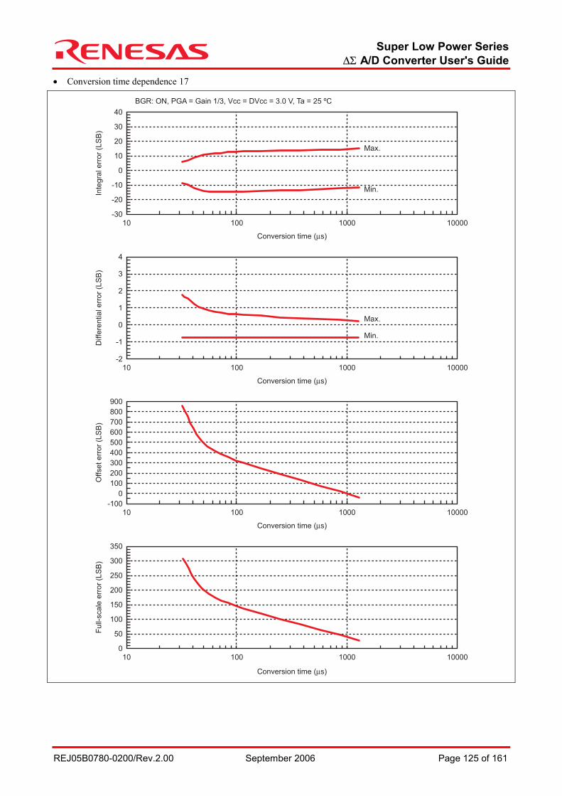
Super Low Power Series ∆Σ A/D Converter User's Guide
REJ05B0780-0200/Rev.2.00 September 2006 Page 125 of 161
• Conversion time dependence 17
Inte
gra
l err
or
(LS
B)
Conversion time (µs)
Diffe
ren
tia
l e
rro
r (L
SB
)
Conversion time (µs)
Offset err
or
(LS
B)
Conversion time (µs)
Fu
ll-sca
le e
rro
r (L
SB
)
Conversion time (µs)
Max.
Min.
Max.
Min.
10
10-2
-1
0
1
2
3
4
10
10
-30
-20
-10
0
10
20
40
30
-100
0
100
200
300
500
700
900
400
600
800
0
50
100
200
300
150
250
350
100 1000 10000
BGR: ON, PGA = Gain 1/3, Vcc = DVcc = 3.0 V, Ta = 25 ºC
100 1000 10000
100 1000 10000
100 1000 10000
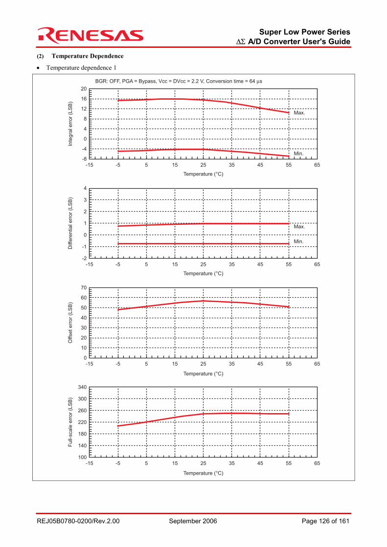
Super Low Power Series ∆Σ A/D Converter User's Guide
REJ05B0780-0200/Rev.2.00 September 2006 Page 126 of 161
(2) Temperature Dependence
• Temperature dependence 1 In
tegra
l err
or
(LS
B)
Temperature (°C)
Diffe
ren
tia
l e
rro
r (L
SB
)
Temperature (°C)
Fu
ll-sca
le e
rro
r (L
SB
)
Temperature (°C)
Offset err
or
(LS
B)
Temperature (°C)
Max.
Min.
Max.
Min.
-15
-2
-1
0
1
2
3
4
-8
-4
0
4
8
12
20
16
0
10
20
30
40
50
70
60
5 35 65-5 25 5515 45
BGR: OFF, PGA = Bypass, Vcc = DVcc = 2.2 V, Conversion time = 64 µs
-15 5 35 65-5 25 5515 45
-15
100
140
180
220
260
300
340
5 35 65-5 25 5515 45
-15 5 35 65-5 25 5515 45
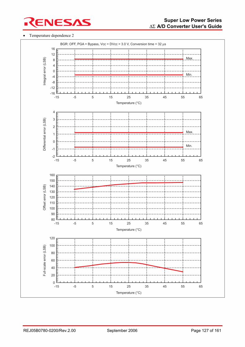
Super Low Power Series ∆Σ A/D Converter User's Guide
REJ05B0780-0200/Rev.2.00 September 2006 Page 127 of 161
• Temperature dependence 2
Inte
gra
l err
or
(LS
B)
Temperature (°C)
Diffe
ren
tia
l e
rro
r (L
SB
)
Temperature (°C)
Fu
ll-sca
le e
rro
r (L
SB
)
Temperature (°C)
Offset err
or
(LS
B)
Temperature (°C)
Max.
Min.
Max.
Min.
-15
-2
-1
0
1
2
3
4
-16
-12
-8
-4
0
4
8
16
12
80
90
100
110
120
130
160
150
140
5 35 65-5 25 5515 45
BGR: OFF, PGA = Bypass, Vcc = DVcc = 3.0 V, Conversion time = 32 µs
-15 5 35 65-5 25 5515 45
-15
0
20
40
60
80
100
120
5 35 65-5 25 5515 45
-15 5 35 65-5 25 5515 45
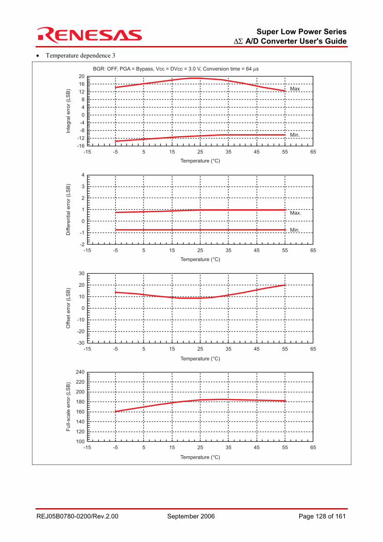
Super Low Power Series ∆Σ A/D Converter User's Guide
REJ05B0780-0200/Rev.2.00 September 2006 Page 128 of 161
• Temperature dependence 3
Inte
gra
l err
or
(LS
B)
Temperature (°C)
Diffe
ren
tia
l e
rro
r (L
SB
)
Temperature (°C)
Fu
ll-sca
le e
rro
r (L
SB
)
Temperature (°C)
Offset err
or
(LS
B)
Temperature (°C)
Max
Min.
Max.
Min.
-15
-2
-1
0
1
2
3
4
-16
-12
-8
-4
0
4
8
20
16
12 .
5 35 65-5 25 5515 45
BGR: OFF, PGA = Bypass, Vcc = DVcc = 3.0 V, Conversion time = 64 µs
-15 5 35 65-5 25 5515 45
-15
100
120
140
160
180
200
240
220
-30
-20
-10
0
10
20
30
5 35 65-5 25 5515 45
-15 5 35 65-5 25 5515 45
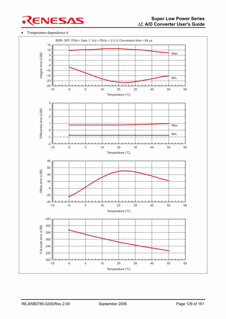
Super Low Power Series ∆Σ A/D Converter User's Guide
REJ05B0780-0200/Rev.2.00 September 2006 Page 129 of 161
• Temperature dependence 4
Inte
gra
l err
or
(LS
B)
Temperature (°C)
Diffe
ren
tia
l e
rro
r (L
SB
)
Temperature (°C)
Fu
ll-sca
le e
rro
r (L
SB
)
Temperature (°C)
Offset err
or
(LS
B)
Temperature (°C)
Max.
Min.
Max.
Min.
-15
-2
-1
0
1
2
3
4
-25
-20
-15
-10
-5
0
5
15
10
5 35 65-5 25 5515 45
BGR: OFF, PGA = Gain 1, Vcc = DVcc = 2.2 V, Conversion time = 64 µs
-15 5 35 65-5 25 5515 45
-15-40
-20
0
20
40
60
80
200
220
240
260
280
300
320
5 35 65-5 25 5515 45
-15 5 35 65-5 25 5515 45

Super Low Power Series ∆Σ A/D Converter User's Guide
REJ05B0780-0200/Rev.2.00 September 2006 Page 130 of 161
• Temperature dependence 5
Inte
gra
l err
or
(LS
B)
Temperature (°C)
Diffe
ren
tia
l e
rro
r (L
SB
)
Temperature (°C)
Fu
ll-sca
le e
rro
r (L
SB
)
Temperature (°C)
Offset err
or
(LS
B)
Temperature (°C)
Max.
Min.
Max.
Min.
-15
-2
-1
0
1
2
3
4
-15
-10
-5
0
5
10
15
30
25
20
5 35 65-5 25 5515 45
BGR: OFF, PGA = Gain 1, Vcc = DVcc = 3.0 V, Conversion time = 32 µs
-15 5 35 65-5 25 5515 45
-1560
80
100
120
160
140
0
20
40
60
80
100
120
5 35 65-5 25 5515 45
-15 5 35 65-5 25 5515 45
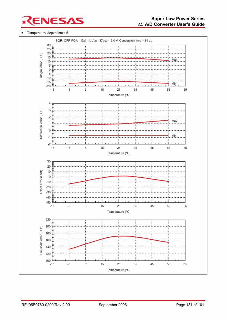
Super Low Power Series ∆Σ A/D Converter User's Guide
REJ05B0780-0200/Rev.2.00 September 2006 Page 131 of 161
• Temperature dependence 6
Inte
gra
l err
or
(LS
B)
Temperature (°C)
Diffe
ren
tia
l e
rro
r (L
SB
)
Temperature (°C)
Fu
ll-sca
le e
rro
r (L
SB
)
Temperature (°C)
Offset err
or
(LS
B)
Temperature (°C)
Max.
Min.
Max.
Min.
-15
-2
-1
0
1
2
3
4
-20
-15
-10
-5
0
5
10
30
25
20
15
5 35 65-5 25 5515 45
BGR: OFF, PGA = Gain 1, Vcc = DVcc = 3.0 V, Conversion time = 64 µs
-15 5 35 65-5 25 5515 45
-15-50
-30
-40
-20
-10
30
10
20
0
100
120
140
160
180
200
220
5 35 65-5 25 5515 45
-15 5 35 65-5 25 5515 45
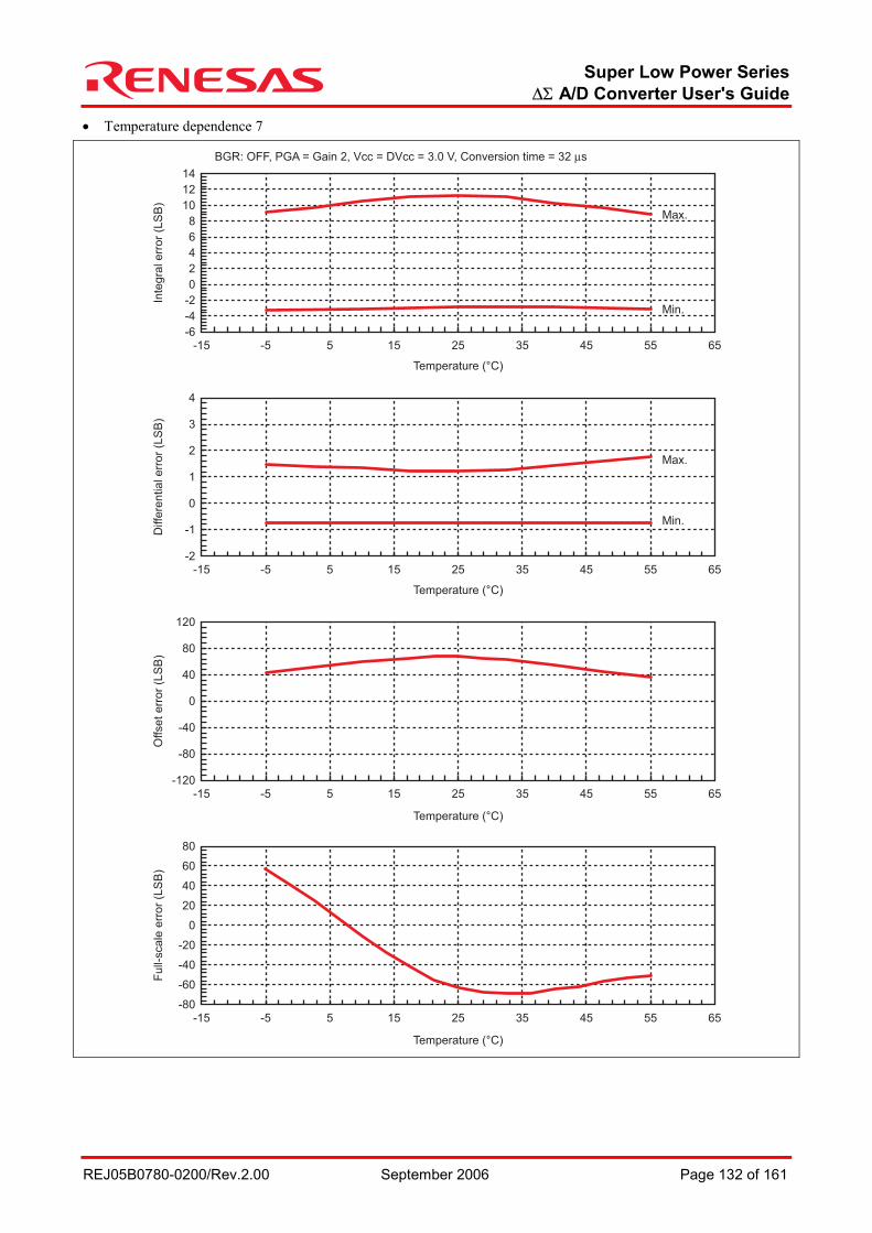
Super Low Power Series ∆Σ A/D Converter User's Guide
REJ05B0780-0200/Rev.2.00 September 2006 Page 132 of 161
• Temperature dependence 7
Inte
gra
l err
or
(LS
B)
Temperature (°C)
Diffe
ren
tia
l e
rro
r (L
SB
)
Temperature (°C)
Fu
ll-sca
le e
rro
r (L
SB
)
Temperature (°C)
Offset err
or
(LS
B)
Temperature (°C)
Max.
Min.
Max.
Min.
-15
-2
-1
0
1
2
3
4
-6
-4
-2
0
2
4
6
14
12
10
8
5 35 65-5 25 5515 45
BGR: OFF, PGA = Gain 2, Vcc = DVcc = 3.0 V, Conversion time = 32 µs
-15 5 35 65-5 25 5515 45
-15
-80
-40
-60
-20
0
80
40
60
20
-120
-80
-40
0
40
80
120
5 35 65-5 25 5515 45
-15 5 35 65-5 25 5515 45
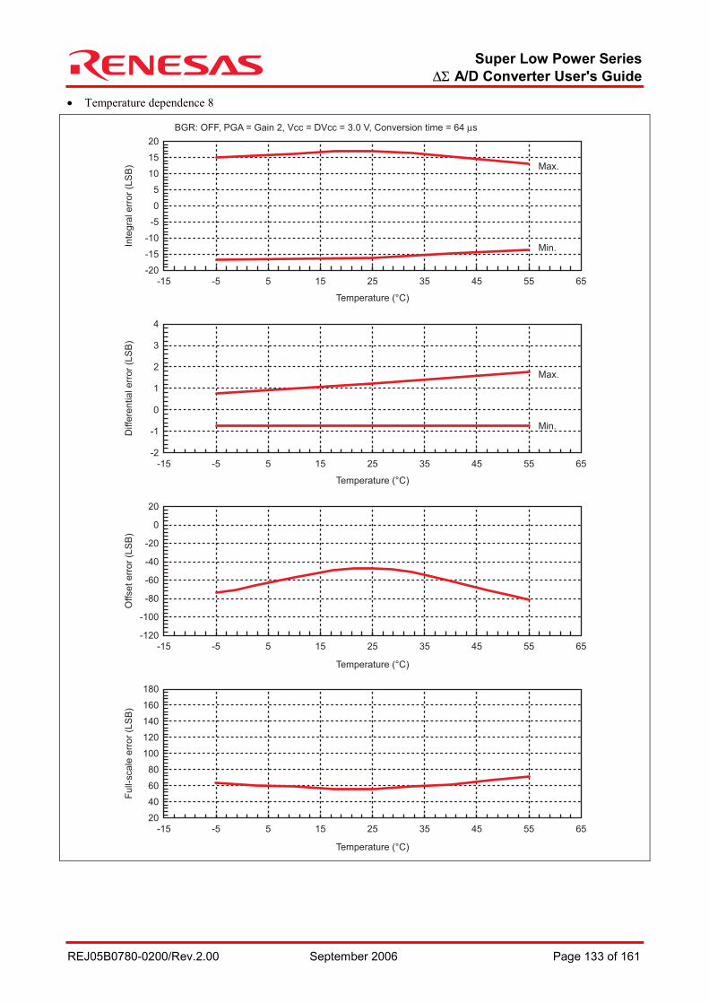
Super Low Power Series ∆Σ A/D Converter User's Guide
REJ05B0780-0200/Rev.2.00 September 2006 Page 133 of 161
• Temperature dependence 8
Inte
gra
l err
or
(LS
B)
Temperature (°C)
Diffe
ren
tia
l e
rro
r (L
SB
)
Temperature (°C)
Fu
ll-sca
le e
rro
r (L
SB
)
Temperature (°C)
Offset err
or
(LS
B)
Temperature (°C)
Max.
Min.
Max.
Min.
-15
-2
-1
0
1
2
3
4
-20
-15
-10
-5
0
5
10
20
15
5 35 65-5 25 5515 45
BGR: OFF, PGA = Gain 2, Vcc = DVcc = 3.0 V, Conversion time = 64 µs
-15 5 35 65-5 25 5515 45
-15
20
60
40
80
100
180
140
160
120
-120
-100
-80
-60
-40
-20
0
20
5 35 65-5 25 5515 45
-15 5 35 65-5 25 5515 45
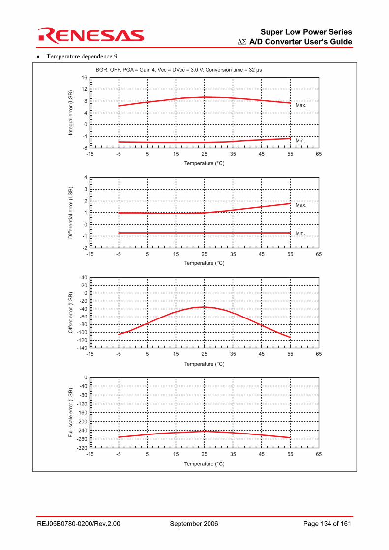
Super Low Power Series ∆Σ A/D Converter User's Guide
REJ05B0780-0200/Rev.2.00 September 2006 Page 134 of 161
• Temperature dependence 9
Inte
gra
l err
or
(LS
B)
Temperature (°C)
Diffe
ren
tia
l e
rro
r (L
SB
)
Temperature (°C)
Fu
ll-sca
le e
rro
r (L
SB
)
Temperature (°C)
Offset err
or
(LS
B)
Temperature (°C)
Max.
Min.
Max.
Min.
-15
-2
-1
0
1
2
3
4
-8
-4
0
4
8
12
16
5 35 65-5 25 5515 45
BGR: OFF, PGA = Gain 4, Vcc = DVcc = 3.0 V, Conversion time = 32 µs
-15 5 35 65-5 25 5515 45
-15
-320
-240
-280
-200
-160
0
-80
-40
-120
-140
0
-120
-100
-80
-40
20
-60
-20
40
5 35 65-5 25 5515 45
-15 5 35 65-5 25 5515 45
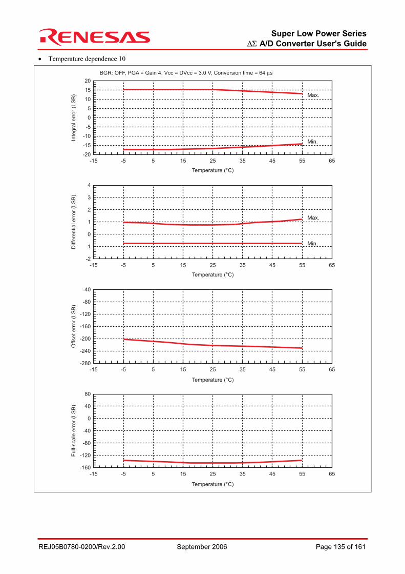
Super Low Power Series ∆Σ A/D Converter User's Guide
REJ05B0780-0200/Rev.2.00 September 2006 Page 135 of 161
• Temperature dependence 10
Inte
gra
l err
or
(LS
B)
Temperature (°C)
Diffe
ren
tia
l e
rro
r (L
SB
)
Temperature (°C)
Fu
ll-sca
le e
rro
r (L
SB
)
Temperature (°C)
Offset err
or
(LS
B)
Temperature (°C)
Max.
Min.
Max.
Min.
-15
-2
-1
0
1
2
3
4
-20
-15
-10
-5
5
15
0
10
20
-280
-240
-200
-160
-120
-80
-40
-160
-120
-80
-40
0
40
80
5 35 65-5 25 5515 45
BGR: OFF, PGA = Gain 4, Vcc = DVcc = 3.0 V, Conversion time = 64 µs
-15 5 35 65-5 25 5515 45
-15 5 35 65-5 25 5515 45
-15 5 35 65-5 25 5515 45
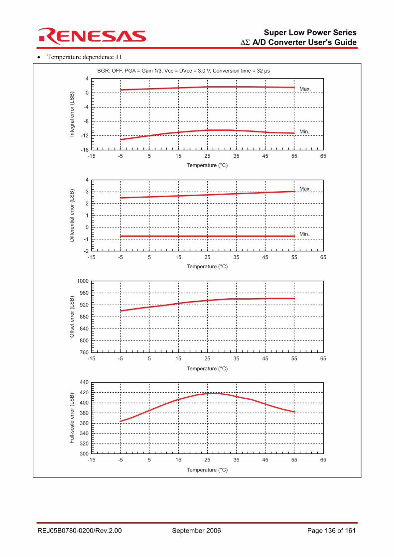
Super Low Power Series ∆Σ A/D Converter User's Guide
REJ05B0780-0200/Rev.2.00 September 2006 Page 136 of 161
• Temperature dependence 11
Inte
gra
l err
or
(LS
B)
Temperature (°C)
Diffe
ren
tia
l e
rro
r (L
SB
)
Temperature (°C)
Fu
ll-sca
le e
rro
r (L
SB
)
Temperature (°C)
Offset err
or
(LS
B)
Temperature (°C)
Max.
Min.
Max.
Min.
-15
-2
-1
0
1
2
3
4
-16
-12
-8
-4
0
4
760
800
840
880
920
960
1000
300
320
340
360
380
400
440
420
5 35 65-5 25 5515 45
BGR: OFF, PGA = Gain 1/3, Vcc = DVcc = 3.0 V, Conversion time = 32 µs
-15 5 35 65-5 25 5515 45
-15 5 35 65-5 25 5515 45
-15 5 35 65-5 25 5515 45
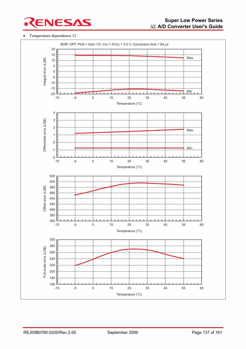
Super Low Power Series ∆Σ A/D Converter User's Guide
REJ05B0780-0200/Rev.2.00 September 2006 Page 137 of 161
• Temperature dependence 12
Inte
gra
l err
or
(LS
B)
Temperature (°C)
Diffe
ren
tia
l e
rro
r (L
SB
)
Temperature (°C)
Fu
ll-sca
le e
rro
r (L
SB
)
Temperature (°C)
Offset err
or
(LS
B)
Temperature (°C)
Max.
Min.
Max.
Min.
-15
-2
-1
0
1
2
3
4
360
380
400
420
440
460
480
500
520
-20
-15
-10
-5
0
5
10
15
20
160
180
200
220
240
260
300
280
5 35 65-5 25 5515 45
BGR: OFF, PGA = Gain 1/3, Vcc = DVcc = 3.0 V, Conversion time = 64 µs
-15 5 35 65-5 25 5515 45
-15 5 35 65-5 25 5515 45
-15 5 35 65-5 25 5515 45
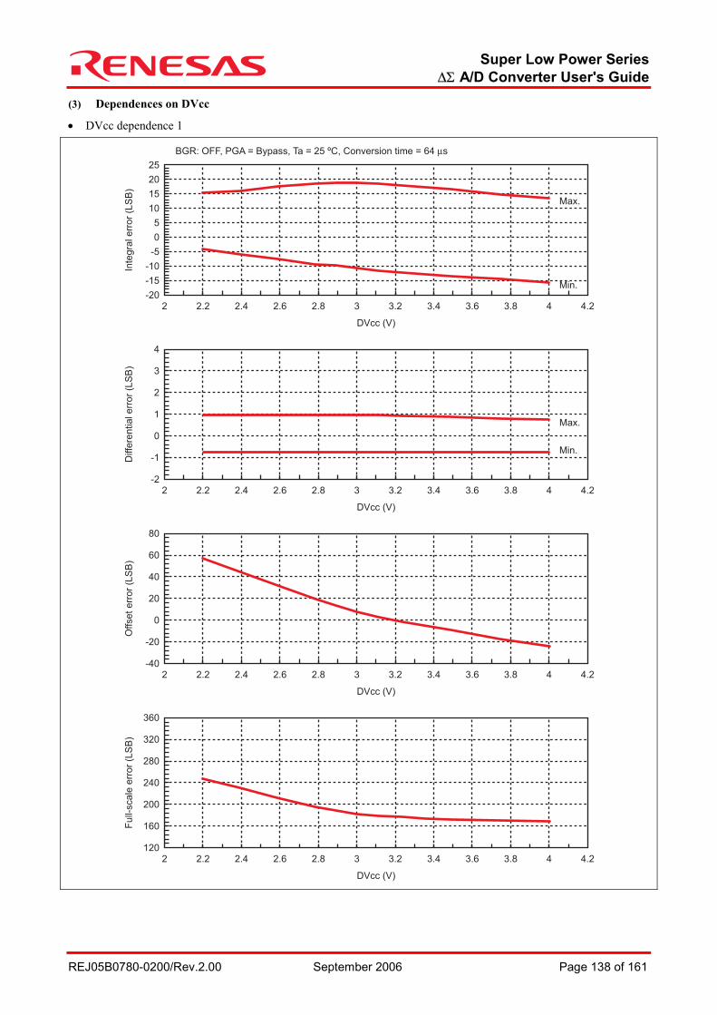
Super Low Power Series ∆Σ A/D Converter User's Guide
REJ05B0780-0200/Rev.2.00 September 2006 Page 138 of 161
(3) Dependences on DVcc
• DVcc dependence 1 In
tegra
l err
or
(LS
B)
Diffe
rential err
or
(LS
B)
Full-
scale
err
or
(LS
B)
Offset err
or
(LS
B)
DVcc (V)
DVcc (V)
DVcc (V)
DVcc (V)
Max.
Min.
Max.
Min.
2
-2
-1
0
1
2
3
4
-20
-15
-10
-5
0
5
10
15
25
20
2.4 3 4.22.2 2.8 3.8 43.63.42.6 3.2
BGR: OFF, PGA = Bypass, Ta = 25 ºC, Conversion time = 64 µs
2 2.4 3 4.22.2 2.8 3.8 43.63.42.6 3.2
2 2.4 3 4.22.2 2.8 3.8 43.63.42.6 3.2
2 2.4 3 4.22.2 2.8 3.8 43.63.42.6 3.2
-40
-20
0
20
40
60
80
120
160
200
240
280
320
360

Super Low Power Series ∆Σ A/D Converter User's Guide
REJ05B0780-0200/Rev.2.00 September 2006 Page 139 of 161
• DVcc dependence 2
Inte
gra
l err
or
(LS
B)
Diffe
rential err
or
(LS
B)
Full-
scale
err
or
(LS
B)
Offset err
or
(LS
B)
DVcc (V)
DVcc (V)
DVcc (V)
DVcc (V)
Max.
Min.
Max.
Min.
2 2.4 3 4.22.2 2.8 3.8 43.63.42.6 3.2
2 2.4 3 4.22.2 2.8 3.8 43.63.42.6 3.2
2 2.4 3 4.22.2 2.8 3.8 43.63.42.6 3.2
2 2.4 3 4.22.2 2.8 3.8 43.63.42.6 3.2
-2
-1
0
1
2
3
4
-25
-20
-15
-10
-5
0
5
10
15
25
20
BGR: OFF, PGA = Gain 1, Ta = 25 ºC, Conversion time = 64 µs
-60
-40
-20
0
20
40
60
80
120
160
200
240
280
320
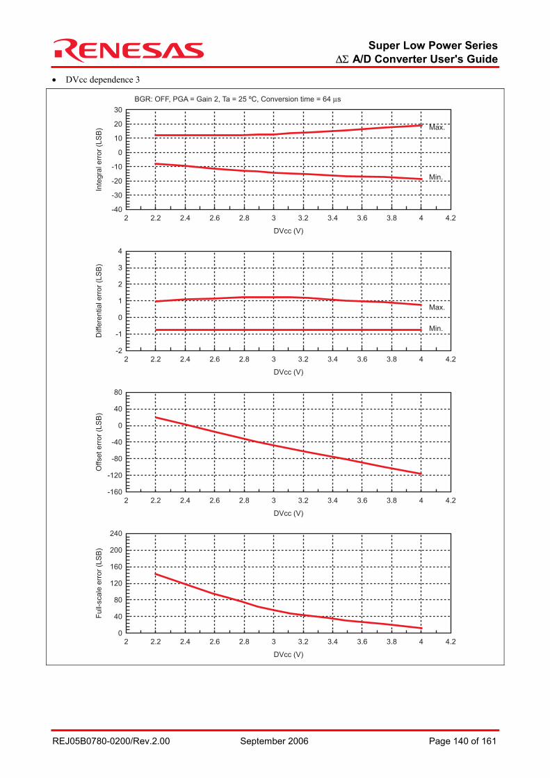
Super Low Power Series ∆Σ A/D Converter User's Guide
REJ05B0780-0200/Rev.2.00 September 2006 Page 140 of 161
• DVcc dependence 3
Inte
gra
l err
or
(LS
B)
Diffe
rential err
or
(LS
B)
Full-
scale
err
or
(LS
B)
Offset err
or
(LS
B)
DVcc (V)
DVcc (V)
DVcc (V)
DVcc (V)
Max.
Min.
Max.
Min.
2.4 3 4.22.2 2.8 3.8 43.63.42.6 3.2
2.4 3 4.22.2 2.8 3.8 43.63.42.6 3.2
2 2.4 3 4.22.2 2.8 3.8 43.63.42.6 3.2
2 2.4 3 4.22.2 2.8 3.8 43.63.42.6 3.2
-2
-1
0
1
2
3
4
2-160
-120
-80
-40
0
40
80
20
40
80
120
160
200
240
-40
-30
-20
-10
0
10
20
30
BGR: OFF, PGA = Gain 2, Ta = 25 ºC, Conversion time = 64 µs
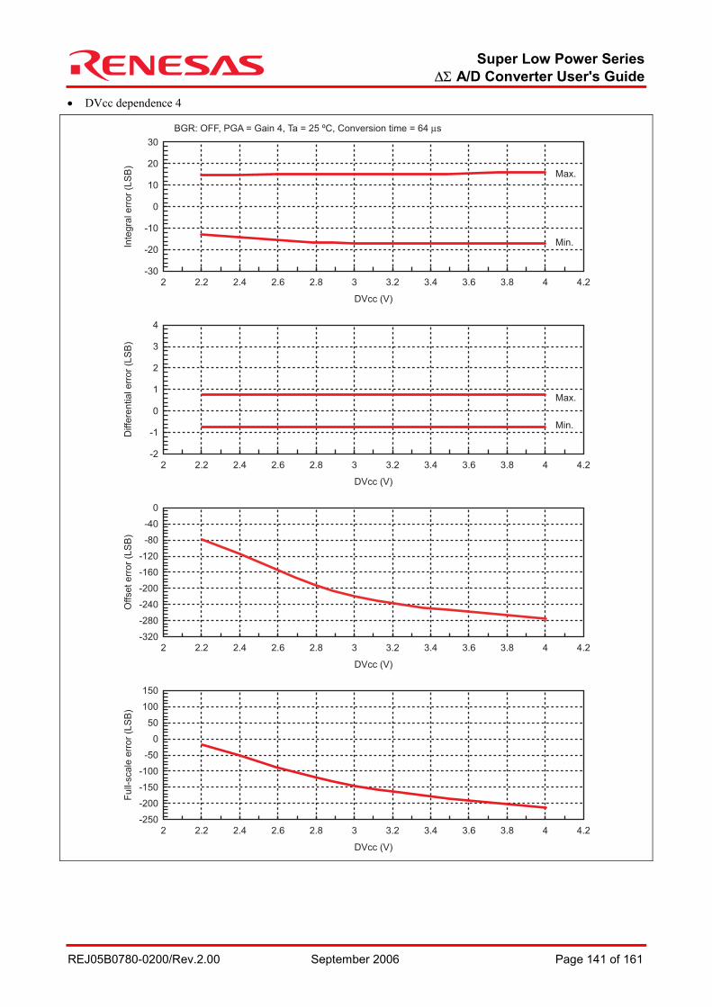
Super Low Power Series ∆Σ A/D Converter User's Guide
REJ05B0780-0200/Rev.2.00 September 2006 Page 141 of 161
• DVcc dependence 4
Inte
gra
l err
or
(LS
B)
Diffe
rential err
or
(LS
B)
Full-
scale
err
or
(LS
B)
Offset err
or
(LS
B)
DVcc (V)
DVcc (V)
DVcc (V)
DVcc (V)
Max.
Min.
Max.
Min.
2.4 3 4.22.2 2.8 3.8 43.63.42.6 3.2
2.4 3 4.22.2 2.8 3.8 43.63.42.6 3.2
2 2.4 3 4.22.2 2.8 3.8 43.63.42.6 3.2
2 2.4 3 4.22.2 2.8 3.8 43.63.42.6 3.2
-2
-1
0
1
2
3
4
2-320
-280
-240
-200
-120
-40
-160
-80
0
-250
-200
-150
-100
0
100
-50
50
150
2
-30
-20
-10
0
10
20
30
BGR: OFF, PGA = Gain 4, Ta = 25 ºC, Conversion time = 64 µs
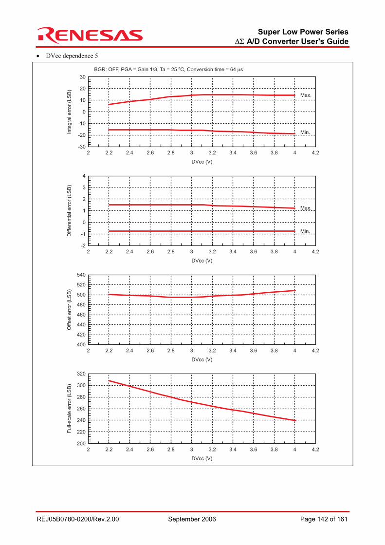
Super Low Power Series ∆Σ A/D Converter User's Guide
REJ05B0780-0200/Rev.2.00 September 2006 Page 142 of 161
• DVcc dependence 5
Inte
gra
l err
or
(LS
B)
Diffe
rential err
or
(LS
B)
Full-
scale
err
or
(LS
B)
Offset err
or
(LS
B)
DVcc (V)
DVcc (V)
DVcc (V)
DVcc (V)
Max.
Min.
Max.
Min.
2.4 3 4.22.2 2.8 3.8 43.63.42.6 3.2
2.4 3 4.22.2 2.8 3.8 43.63.42.6 3.2
2 2.4 3 4.22.2 2.8 3.8 43.63.42.6 3.2
2 2.4 3 4.22.2 2.8 3.8 43.63.42.6 3.2
-2
-1
0
1
2
3
4
200
220
240
260
280
300
320
2400
420
440
480
520
460
500
540
2
-30
-20
-10
0
10
20
30
BGR: OFF, PGA = Gain 1/3, Ta = 25 ºC, Conversion time = 64 µs
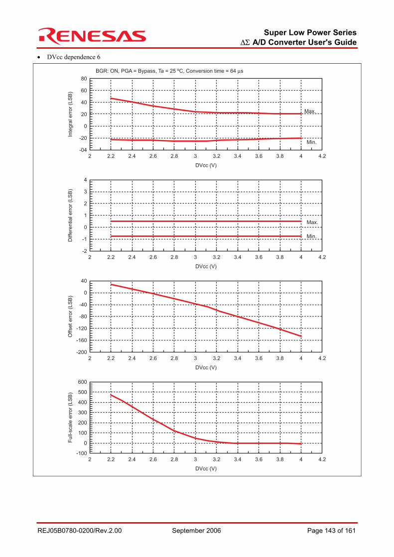
Super Low Power Series ∆Σ A/D Converter User's Guide
REJ05B0780-0200/Rev.2.00 September 2006 Page 143 of 161
• DVcc dependence 6
Inte
gra
l err
or
(LS
B)
Diffe
rential err
or
(LS
B)
Full-
scale
err
or
(LS
B)
Offset err
or
(LS
B)
DVcc (V)
DVcc (V)
DVcc (V)
DVcc (V)
Max.
Min.
Max.
Min.
2.4 3 4.22.2 2.8 3.8 43.63.42.6 3.2
2.4 3 4.22.2 2.8 3.8 43.63.42.6 3.2
2 2.4 3 4.22.2 2.8 3.8 43.63.42.6 3.2
2 2.4 3 4.22.2 2.8 3.8 43.63.42.6 3.2
-2
-1
0
1
2
3
4
-200
-160
-120
-80
-40
0
40
2
-100
0
100
300
500
200
400
600
2
-04
-20
0
20
40
60
80
BGR: ON, PGA = Bypass, Ta = 25 ºC, Conversion time = 64 µs
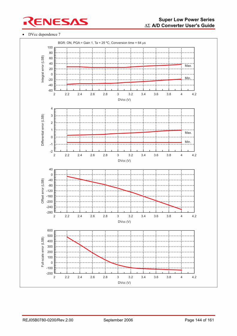
Super Low Power Series ∆Σ A/D Converter User's Guide
REJ05B0780-0200/Rev.2.00 September 2006 Page 144 of 161
• DVcc dependence 7
Inte
gra
l err
or
(LS
B)
Diffe
rential err
or
(LS
B)
Full-
scale
err
or
(LS
B)
Offset err
or
(LS
B)
DVcc (V)
DVcc (V)
DVcc (V)
DVcc (V)
Max.
Min.
Max.
Min.
2.4 3 4.22.2 2.8 3.8 43.63.42.6 3.2
2.4 3 4.22.2 2.8 3.8 43.63.42.6 3.2
2 2.4 3 4.22.2 2.8 3.8 43.63.42.6 3.2
2 2.4 3 4.22.2 2.8 3.8 43.63.42.6 3.2
-2
-1
0
1
2
3
4
2
2
-60
-40
-20
0
20
60
100
40
80
-280
-240
-200
-160
-120
-40
40
-80
0
-200
-100
0
100
200
400
600
300
500
BGR: ON, PGA = Gain 1, Ta = 25 ºC, Conversion time = 64 µs
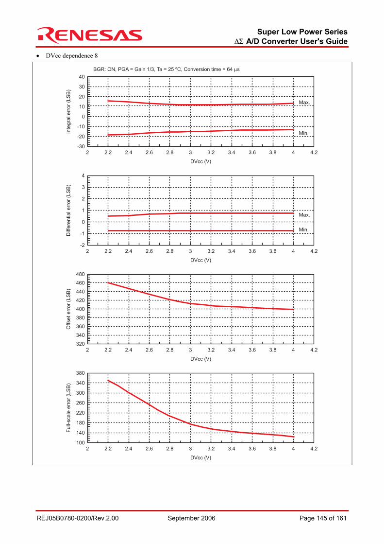
Super Low Power Series ∆Σ A/D Converter User's Guide
REJ05B0780-0200/Rev.2.00 September 2006 Page 145 of 161
• DVcc dependence 8
Inte
gra
l err
or
(LS
B)
Diffe
rential err
or
(LS
B)
Full-
scale
err
or
(LS
B)
Offset err
or
(LS
B)
DVcc (V)
DVcc (V)
DVcc (V)
DVcc (V)
Max.
Min.
Max.
Min.
2.4 3 4.22.2 2.8 3.8 43.63.42.6 3.2
2.4 3 4.22.2 2.8 3.8 43.63.42.6 3.2
2 2.4 3 4.22.2 2.8 3.8 43.63.42.6 3.2
2 2.4 3 4.22.2 2.8 3.8 43.63.42.6 3.2
-2
-1
0
1
2
3
4
2
2
-30
-20
-10
0
10
30
40
20
100
140
180
220
260
340
380
300
320
340
360
380
400
440
480
420
460
BGR: ON, PGA = Gain 1/3, Ta = 25 ºC, Conversion time = 64 µs
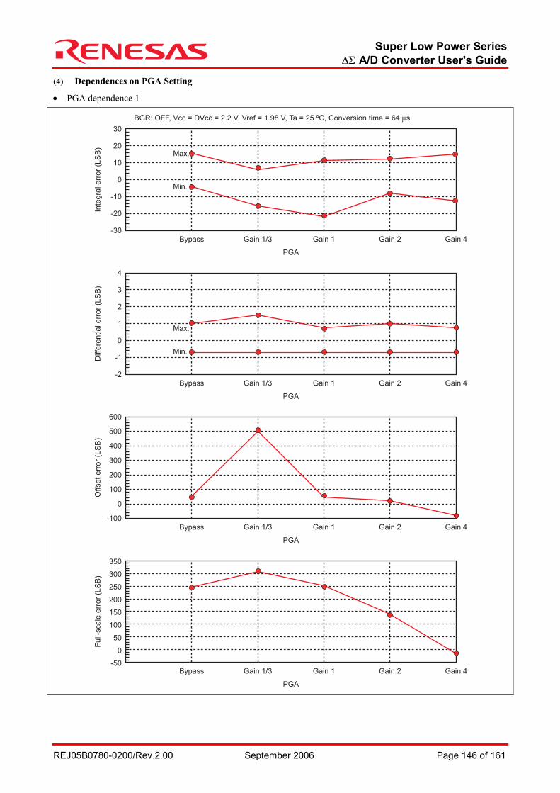
Super Low Power Series ∆Σ A/D Converter User's Guide
REJ05B0780-0200/Rev.2.00 September 2006 Page 146 of 161
(4) Dependences on PGA Setting
• PGA dependence 1
Gain 1Gain 1/3 Gain 4Bypass Gain 2
PGA
Gain 1Gain 1/3 Gain 4Bypass Gain 2
PGA
Gain 1Gain 1/3 Gain 4Bypass Gain 2
PGA
Gain 1Gain 1/3 Gain 4Bypass Gain 2
PGA
Inte
gra
l err
or
(LS
B)
Diffe
rential err
or
(LS
B)
Full-
scale
err
or
(LS
B)
Offset err
or
(LS
B)
Max.
Min.
Max.
Min.
-50
0
50
100
150
200
250
300
350
BGR: OFF, Vcc = DVcc = 2.2 V, Vref = 1.98 V, Ta = 25 ºC, Conversion time = 64 µs
-30
10
0
-10
-20
30
20
-100
500
300
400
200
100
0
600
-2
2
1
0
-1
4
3

Super Low Power Series ∆Σ A/D Converter User's Guide
REJ05B0780-0200/Rev.2.00 September 2006 Page 147 of 161
• PGA dependence 2
Inte
gra
l err
or
(LS
B)
Diffe
rential err
or
(LS
B)
Full-
scale
err
or
(LS
B)
Offset err
or
(LS
B)
Gain 1Gain 1/3 Gain 4Bypass Gain 2
-300
-200
-100
0
100
200
300
400
500
PGA
BGR: OFF, Vcc = DVcc = 3.0 V, Vref = 1.9 8V, Ta = 25 ºC, Conversion time = 32 µs
-30
10
0
-10
-20
30
20
Gain 1Gain 1/3 Gain 4Bypass Gain 2
PGA
Gain 1Gain 1/3 Gain 4Bypass Gain 2
PGA
Gain 1Gain 1/3 Gain 4Bypass Gain 2
PGA
-100
900
500
700
800
400
600
300
200
100
0
1000
-2
2
1
0
-1
4
3
Max.
Min.
Max.
Min.
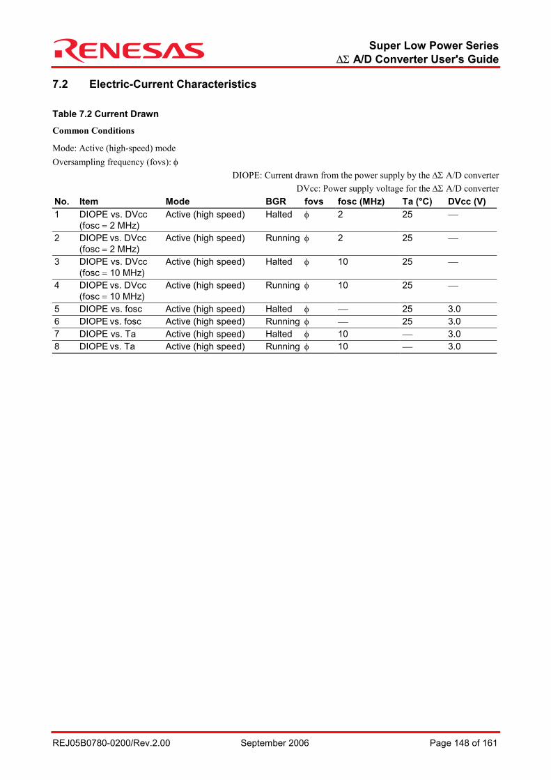
Super Low Power Series ∆Σ A/D Converter User's Guide
REJ05B0780-0200/Rev.2.00 September 2006 Page 148 of 161
7.2 Electric-Current Characteristics Table 7.2 Current Drawn
Common Conditions
Mode: Active (high-speed) mode Oversampling frequency (fovs): φ
DIOPE: Current drawn from the power supply by the ∆Σ A/D converter DVcc: Power supply voltage for the ∆Σ A/D converter
No. Item Mode BGR fovs fosc (MHz) Ta (°C) DVcc (V) 1 DIOPE vs. DVcc
(fosc = 2 MHz) Active (high speed) Halted φ 2 25
2 DIOPE vs. DVcc (fosc = 2 MHz)
Active (high speed) Running φ 2 25
3 DIOPE vs. DVcc (fosc = 10 MHz)
Active (high speed) Halted φ 10 25
4 DIOPE vs. DVcc (fosc = 10 MHz)
Active (high speed) Running φ 10 25
5 DIOPE vs. fosc Active (high speed) Halted φ 25 3.0 6 DIOPE vs. fosc Active (high speed) Running φ 25 3.0 7 DIOPE vs. Ta Active (high speed) Halted φ 10 3.0 8 DIOPE vs. Ta Active (high speed) Running φ 10 3.0
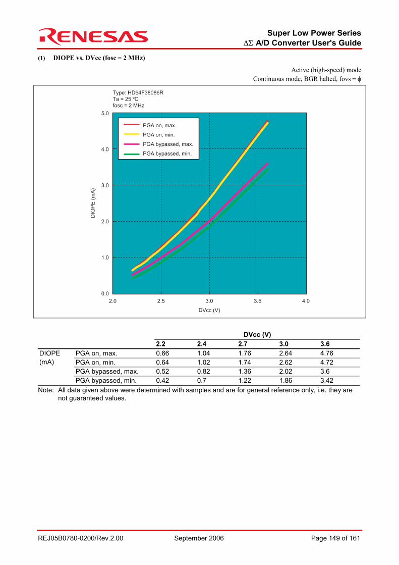
Super Low Power Series ∆Σ A/D Converter User's Guide
REJ05B0780-0200/Rev.2.00 September 2006 Page 149 of 161
(1) DIOPE vs. DVcc (fosc = 2 MHz)
Active (high-speed) mode Continuous mode, BGR halted, fovs = φ
5.0
4.0
3.0
2.0
1.0
0.0
2.0 2.5 3.0
DVcc (V)
DIO
PE
(m
A)
Type: HD64F38086R
Ta = 25 ºC
fosc = 2 MHz
3.5 4.0
PGA on, max.
PGA on, min.
PGA bypassed, max.
PGA bypassed, min.
DVcc (V)
2.2 2.4 2.7 3.0 3.6 PGA on, max. 0.66 1.04 1.76 2.64 4.76 PGA on, min. 0.64 1.02 1.74 2.62 4.72 PGA bypassed, max. 0.52 0.82 1.36 2.02 3.6
DIOPE (mA)
PGA bypassed, min. 0.42 0.7 1.22 1.86 3.42 Note: All data given above were determined with samples and are for general reference only, i.e. they are
not guaranteed values.
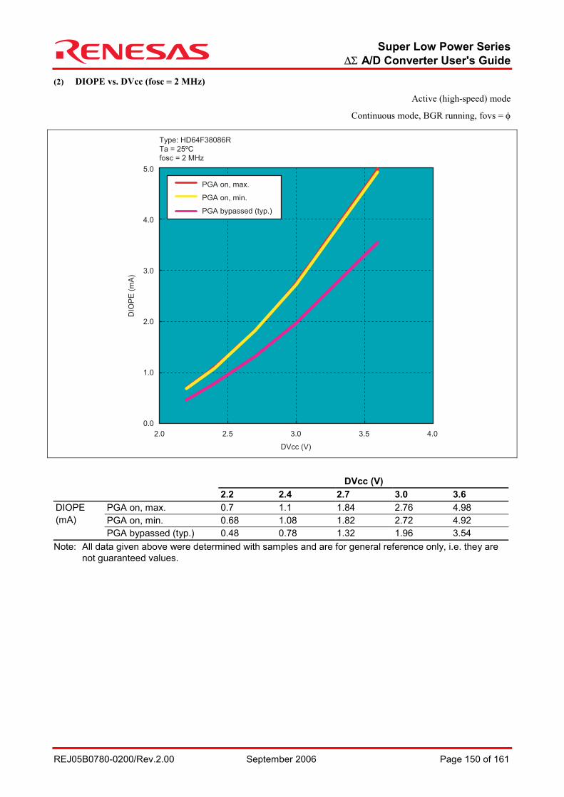
Super Low Power Series ∆Σ A/D Converter User's Guide
REJ05B0780-0200/Rev.2.00 September 2006 Page 150 of 161
(2) DIOPE vs. DVcc (fosc = 2 MHz)
Active (high-speed) mode
Continuous mode, BGR running, fovs = φ
5.0
4.0
3.0
2.0
1.0
0.0
2.0 2.5 3.0
DVcc (V)
DIO
PE
(m
A)
Type: HD64F38086R
Ta = 25ºC
fosc = 2 MHz
3.5 4.0
PGA on, max.
PGA on, min.
PGA bypassed (typ.)
DVcc (V)
2.2 2.4 2.7 3.0 3.6 PGA on, max. 0.7 1.1 1.84 2.76 4.98 PGA on, min. 0.68 1.08 1.82 2.72 4.92
DIOPE (mA)
PGA bypassed (typ.) 0.48 0.78 1.32 1.96 3.54 Note: All data given above were determined with samples and are for general reference only, i.e. they are
not guaranteed values.
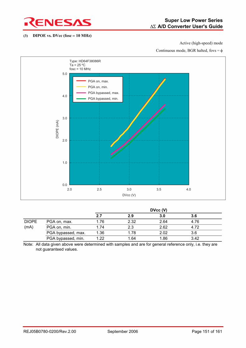
Super Low Power Series ∆Σ A/D Converter User's Guide
REJ05B0780-0200/Rev.2.00 September 2006 Page 151 of 161
(3) DIPOE vs. DVcc (fosc = 10 MHz)
Active (high-speed) mode
Continuous mode, BGR halted, fovs = φ
5.0
4.0
3.0
2.0
1.0
0.0
2.0 2.5 3.0
DVcc (V)
DIO
PE
(m
A)
Type: HD64F38086R
Ta = 25 ºC
fosc = 10 MHz
3.5 4.0
PGA on, max.
PGA on, min.
PGA bypassed, max.
PGA bypassed, min.
DVcc (V)
2.7 2.9 3.0 3.6 PGA on, max. 1.76 2.32 2.64 4.76 PGA on, min. 1.74 2.3 2.62 4.72 PGA bypassed, max. 1.36 1.78 2.02 3.6
DIOPE (mA)
PGA bypassed, min. 1.22 1.64 1.86 3.42 Note: All data given above were determined with samples and are for general reference only, i.e. they are
not guaranteed values.

Super Low Power Series ∆Σ A/D Converter User's Guide
REJ05B0780-0200/Rev.2.00 September 2006 Page 152 of 161
(4) DIOPE vs. DVcc (fosc = 10 MHz)
Active (high-speed) mode
Continuous mode, BGR running, fovs = φ
5.0
4.0
3.0
2.0
1.0
0.0
2.0 2.5 3.0
DVcc (V)
DIO
PE
(m
A)
Type: HD64F38086R
Ta = 25ºC
fosc = 10 MHz
3.5 4.0
PGA on, max.
PGA on, min.
PGA bypassed (typ.)
DVcc (V)
2.7 2.9 3.0 3.6 PGA on, max. 1.84 2.44 2.76 4.98 PGA on, min. 1.82 2.4 2.72 4.92
DIOPE (mA)
PGA bypassed, typ. 1.32 1.74 1.96 3.54 Note: All data given above were determined with samples and are for general reference only, i.e. they are
not guaranteed values.
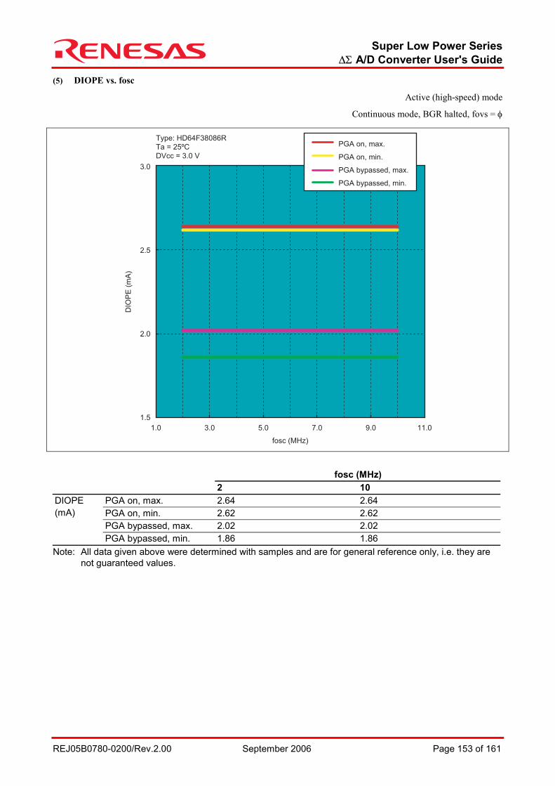
Super Low Power Series ∆Σ A/D Converter User's Guide
REJ05B0780-0200/Rev.2.00 September 2006 Page 153 of 161
(5) DIOPE vs. fosc
Active (high-speed) mode
Continuous mode, BGR halted, fovs = φ
3.0
2.5
2.0
1.5
1.0 3.0 5.0
fosc (MHz)
DIO
PE
(m
A)
Type: HD64F38086R
Ta = 25ºC
DVcc = 3.0 V
7.0 9.0 11.0
PGA on, max.
PGA on, min.
PGA bypassed, max.
PGA bypassed, min.
fosc (MHz)
2 10 PGA on, max. 2.64 2.64 PGA on, min. 2.62 2.62 PGA bypassed, max. 2.02 2.02
DIOPE (mA)
PGA bypassed, min. 1.86 1.86 Note: All data given above were determined with samples and are for general reference only, i.e. they are
not guaranteed values.
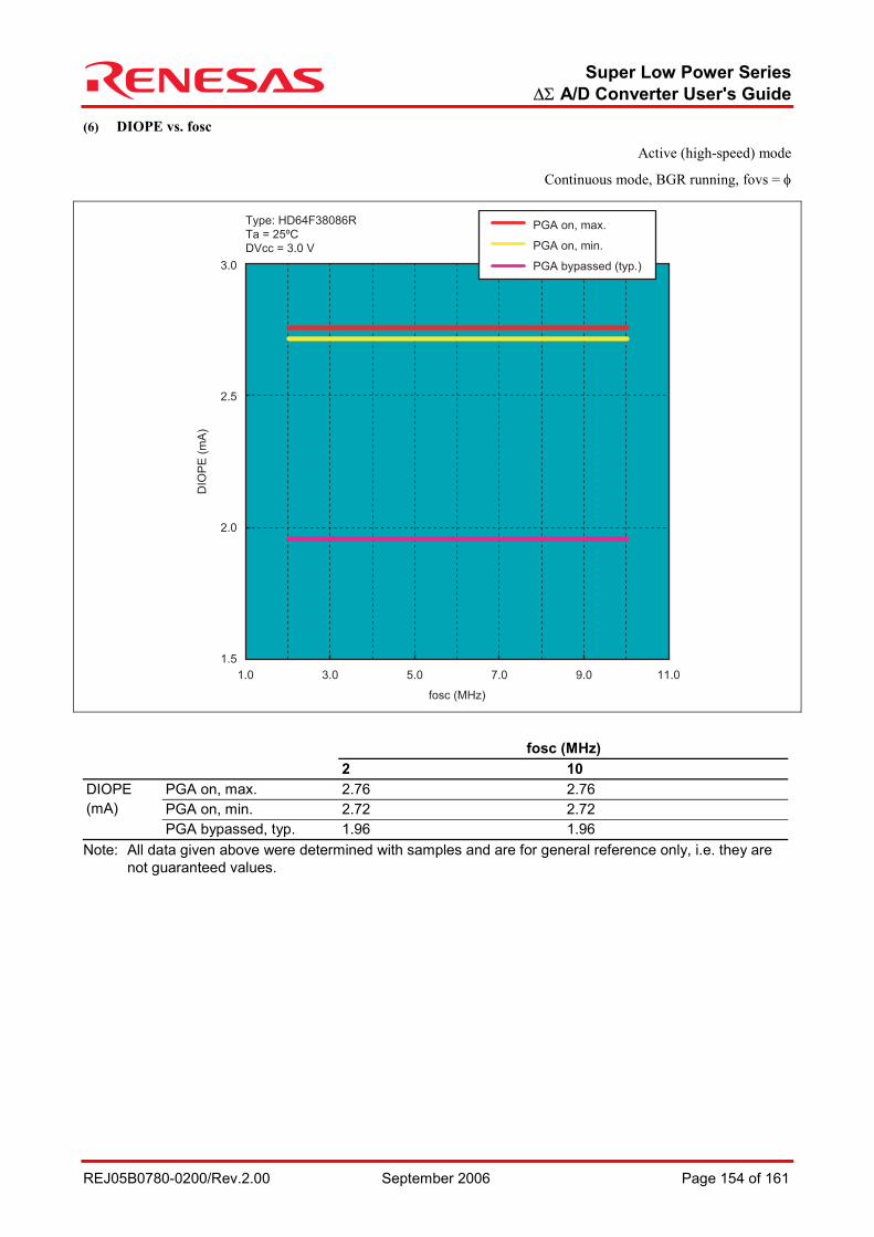
Super Low Power Series ∆Σ A/D Converter User's Guide
REJ05B0780-0200/Rev.2.00 September 2006 Page 154 of 161
(6) DIOPE vs. fosc
Active (high-speed) mode
Continuous mode, BGR running, fovs = φ
3.0
2.5
2.0
1.5
1.0 3.0 5.0
fosc (MHz)
DIO
PE
(m
A)
Type: HD64F38086R
Ta = 25ºC
DVcc = 3.0 V
7.0 9.0 11.0
PGA on, max.
PGA on, min.
PGA bypassed (typ.)
fosc (MHz)
2 10 PGA on, max. 2.76 2.76 PGA on, min. 2.72 2.72
DIOPE (mA)
PGA bypassed, typ. 1.96 1.96 Note: All data given above were determined with samples and are for general reference only, i.e. they are
not guaranteed values.
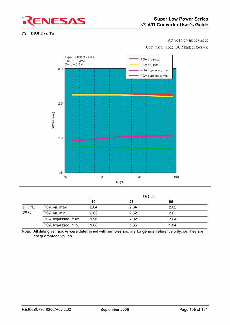
Super Low Power Series ∆Σ A/D Converter User's Guide
REJ05B0780-0200/Rev.2.00 September 2006 Page 155 of 161
(7) DIOPE vs. Ta
Active (high-speed) mode
Continuous mode, BGR halted, fovs = φ
-50 0 50 100
3.0
2.5
2.0
1.5
Ta (ºC)
DIO
PE
(m
A)
Type: HD64F38086R
fosc = 10 MHz
DVcc = 3.0 V
PGA on, max.
PGA on, min.
PGA bypassed, max.
PGA bypassed, min.
Ta (°C)
-40 25 95 PGA on, max. 2.64 2.64 2.62 PGA on, min. 2.62 2.62 2.6 PGA bypassed, max. 1.96 2.02 2.04
DIOPE (mA)
PGA bypassed, min. 1.88 1.86 1.84 Note: All data given above were determined with samples and are for general reference only, i.e. they are
not guaranteed values.
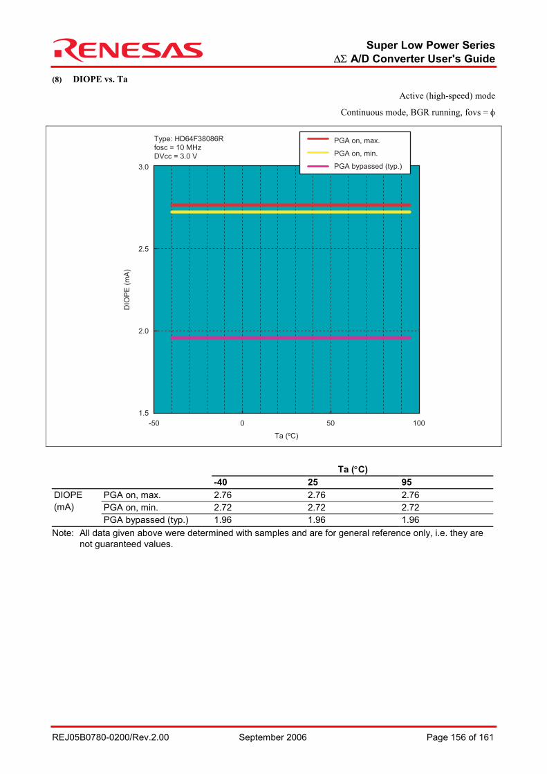
Super Low Power Series ∆Σ A/D Converter User's Guide
REJ05B0780-0200/Rev.2.00 September 2006 Page 156 of 161
(8) DIOPE vs. Ta
Active (high-speed) mode
Continuous mode, BGR running, fovs = φ
-50 0 50 100
3.0
2.5
2.0
1.5
Ta (ºC)
DIO
PE
(m
A)
Type: HD64F38086R
fosc = 10 MHz
DVcc = 3.0 V
PGA on, max.
PGA on, min.
PGA bypassed (typ.)
Ta (°C)
-40 25 95 PGA on, max. 2.76 2.76 2.76 PGA on, min. 2.72 2.72 2.72
DIOPE (mA)
PGA bypassed (typ.) 1.96 1.96 1.96 Note: All data given above were determined with samples and are for general reference only, i.e. they are
not guaranteed values.
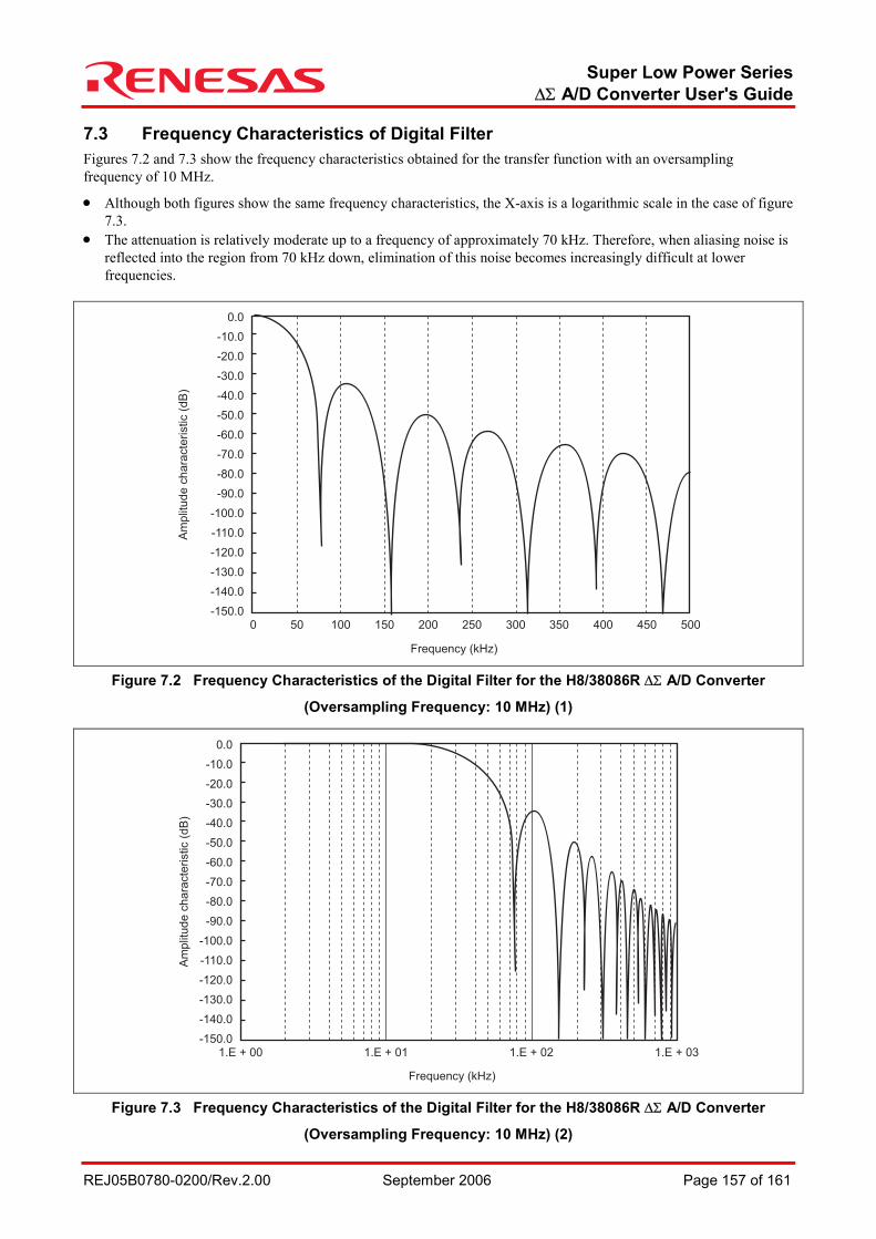
Super Low Power Series ∆Σ A/D Converter User's Guide
REJ05B0780-0200/Rev.2.00 September 2006 Page 157 of 161
7.3 Frequency Characteristics of Digital Filter Figures 7.2 and 7.3 show the frequency characteristics obtained for the transfer function with an oversampling frequency of 10 MHz.
• Although both figures show the same frequency characteristics, the X-axis is a logarithmic scale in the case of figure 7.3.
• The attenuation is relatively moderate up to a frequency of approximately 70 kHz. Therefore, when aliasing noise is reflected into the region from 70 kHz down, elimination of this noise becomes increasingly difficult at lower frequencies.
0.0
-10.0
-20.0
-30.0
-40.0
-50.0
-60.0
-70.0
-80.0
-90.0
-100.0
-110.0
-120.0
-130.0
-140.0
-150.00 50 100 150 200 250 300 350 400 450 500
Am
plit
ud
e c
ha
racte
ristic (
dB
)
Frequency (kHz)
Figure 7.2 Frequency Characteristics of the Digital Filter for the H8/38086R ∆Σ A/D Converter
(Oversampling Frequency: 10 MHz) (1)
0.0
-10.0
-20.0
-30.0
-40.0
-50.0
-60.0
-70.0
-80.0
-90.0
-100.0
-110.0
-120.0
-130.0
-140.0
-150.01.E + 00 1.E + 01
Frequency (kHz)
Am
plit
ud
e c
ha
racte
ristic (
dB
)
1.E + 02 1.E + 03
Figure 7.3 Frequency Characteristics of the Digital Filter for the H8/38086R ∆Σ A/D Converter
(Oversampling Frequency: 10 MHz) (2)
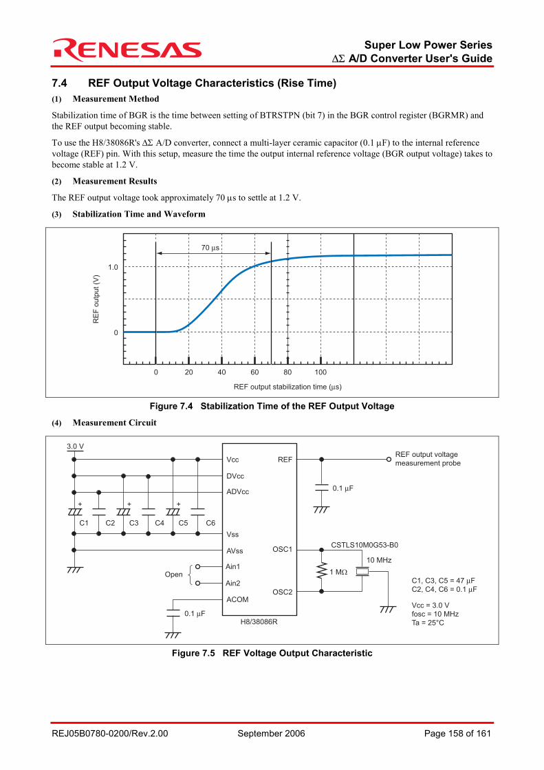
Super Low Power Series ∆Σ A/D Converter User's Guide
REJ05B0780-0200/Rev.2.00 September 2006 Page 158 of 161
7.4 REF Output Voltage Characteristics (Rise Time) (1) Measurement Method
Stabilization time of BGR is the time between setting of BTRSTPN (bit 7) in the BGR control register (BGRMR) and the REF output becoming stable.
To use the H8/38086R's ∆Σ A/D converter, connect a multi-layer ceramic capacitor (0.1 µF) to the internal reference voltage (REF) pin. With this setup, measure the time the output internal reference voltage (BGR output voltage) takes to become stable at 1.2 V.
(2) Measurement Results
The REF output voltage took approximately 70 µs to settle at 1.2 V.
(3) Stabilization Time and Waveform
0
1.0
0 20 40
70 µs
60 80 100
REF output stabilization time (µs)
RE
F o
utp
ut (V
)
Figure 7.4 Stabilization Time of the REF Output Voltage
(4) Measurement Circuit
Ain1Open
Vcc
C6C5
Vss
H8/38086R
C1, C3, C5 = 47 µF
C2, C4, C6 = 0.1 µF
Vcc = 3.0 V
fosc = 10 MHz
Ta = 25°C
0.1 µF
0.1 µF
REF output voltage
measurement probe
+
Ain2
C4C3
+
C2
+
C1
3.0 V
AVss
ACOM
10 MHz
CSTLS10M0G53-B0
1 MΩ
DVcc
ADVcc
OSC2
OSC1
REF
Figure 7.5 REF Voltage Output Characteristic
Super Low Power Series ∆Σ A/D Converter User's Guide
REJ05B0780-0200/Rev.2.00 September 2006 Page 159 of 161
(5) Usage Note
The REF output pin does not have sufficient driving capability. If the REF voltage is to be used externally, include an element that has a high input impedance to amplify the current.
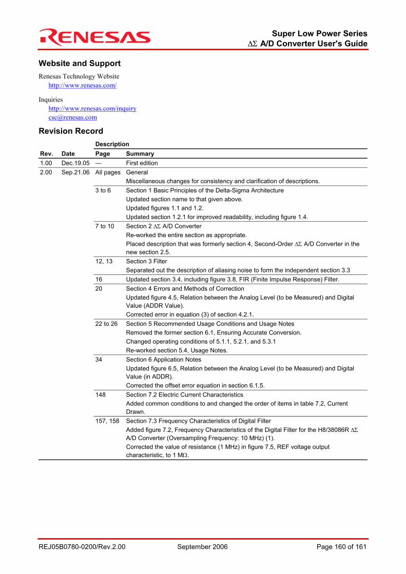
Super Low Power Series ∆Σ A/D Converter User's Guide
REJ05B0780-0200/Rev.2.00 September 2006 Page 160 of 161
Website and Support Renesas Technology Website
http://www.renesas.com/ Inquiries
http://www.renesas.com/inquiry [email protected]
Revision Record
Description Rev. Date Page Summary 1.00 Dec.19.05 — First edition
All pages General Miscellaneous changes for consistency and clarification of descriptions.
3 to 6 Section 1 Basic Principles of the Delta-Sigma Architecture Updated section name to that given above. Updated figures 1.1 and 1.2. Updated section 1.2.1 for improved readability, including figure 1.4.
7 to 10 Section 2 ∆Σ A/D Converter Re-worked the entire section as appropriate. Placed description that was formerly section 4, Second-Order ∆Σ A/D Converter in the new section 2.5.
12, 13 Section 3 Filter Separated out the description of aliasing noise to form the independent section 3.3
16 Updated section 3.4, including figure 3.8, FIR (Finite Impulse Response) Filter. 20 Section 4 Errors and Methods of Correction
Updated figure 4.5, Relation between the Analog Level (to be Measured) and Digital Value (ADDR Value). Corrected error in equation (3) of section 4.2.1.
22 to 26 Section 5 Recommended Usage Conditions and Usage Notes Removed the former section 6.1, Ensuring Accurate Conversion. Changed operating conditions of 5.1.1, 5.2.1, and 5.3.1 Re-worked section 5.4, Usage Notes.
34 Section 6 Application Notes Updated figure 6.5, Relation between the Analog Level (to be Measured) and Digital Value (in ADDR). Corrected the offset error equation in section 6.1.5.
148 Section 7.2 Electric Current Characteristics Added common conditions to and changed the order of items in table 7.2, Current Drawn.
2.00 Sep.21.06
157, 158 Section 7.3 Frequency Characteristics of Digital Filter Added figure 7.2, Frequency Characteristics of the Digital Filter for the H8/38086R ∆Σ A/D Converter (Oversampling Frequency: 10 MHz) (1). Corrected the value of resistance (1 MHz) in figure 7.5, REF voltage output characteristic, to 1 MΩ.
Super Low Power Series ∆Σ A/D Converter User's Guide
REJ05B0780-0200/Rev.2.00 September 2006 Page 161 of 161
1. These materials are intended as a reference to assist our customers in the selection of the Renesas
Technology Corp. product best suited to the customer's application; they do not convey any license
under any intellectual property rights, or any other rights, belonging to Renesas Technology Corp. or
a third party.
2. Renesas Technology Corp. assumes no responsibility for any damage, or infringement of any third-
party's rights, originating in the use of any product data, diagrams, charts, programs, algorithms, or
circuit application examples contained in these materials.
3. All information contained in these materials, including product data, diagrams, charts, programs and
algorithms represents information on products at the time of publication of these materials, and are
subject to change by Renesas Technology Corp. without notice due to product improvements or
other reasons. It is therefore recommended that customers contact Renesas Technology Corp. or
an authorized Renesas Technology Corp. product distributor for the latest product information
before purchasing a product listed herein.
The information described here may contain technical inaccuracies or typographical errors.
Renesas Technology Corp. assumes no responsibility for any damage, liability, or other loss rising
from these inaccuracies or errors.
Please also pay attention to information published by Renesas Technology Corp. by various means,
including the Renesas Technology Corp. Semiconductor home page (http://www.renesas.com).
4. When using any or all of the information contained in these materials, including product data,
diagrams, charts, programs, and algorithms, please be sure to evaluate all information as a total
system before making a final decision on the applicability of the information and products. Renesas
Technology Corp. assumes no responsibility for any damage, liability or other loss resulting from the
information contained herein.
5. Renesas Technology Corp. semiconductors are not designed or manufactured for use in a device or
system that is used under circumstances in which human life is potentially at stake. Please contact
Renesas Technology Corp. or an authorized Renesas Technology Corp. product distributor when
considering the use of a product contained herein for any specific purposes, such as apparatus or
systems for transportation, vehicular, medical, aerospace, nuclear, or undersea repeater use.
6. The prior written approval of Renesas Technology Corp. is necessary to reprint or reproduce in
whole or in part these materials.
7. If these products or technologies are subject to the Japanese export control restrictions, they must
be exported under a license from the Japanese government and cannot be imported into a country
other than the approved destination.
Any diversion or reexport contrary to the export control laws and regulations of Japan and/or the
country of destination is prohibited.
8. Please contact Renesas Technology Corp. for further details on these materials or the products
contained therein.
1. Renesas Technology Corp. puts the maximum effort into making semiconductor products better and
more reliable, but there is always the possibility that trouble may occur with them. Trouble with
semiconductors may lead to personal injury, fire or property damage.
Remember to give due consideration to safety when making your circuit designs, with appropriate
measures such as (i) placement of substitutive, auxiliary circuits, (ii) use of nonflammable material or
(iii) prevention against any malfunction or mishap.
Keep safety first in your circuit designs!
Notes regarding these materials
2006. Renesas Technology Corp., All rights reserved.