STF13NM60N, STI13NM60N, STP13NM60N, STU13NM60N, STW13NM60N · 2017-08-08 · STF13NM60N,...
21
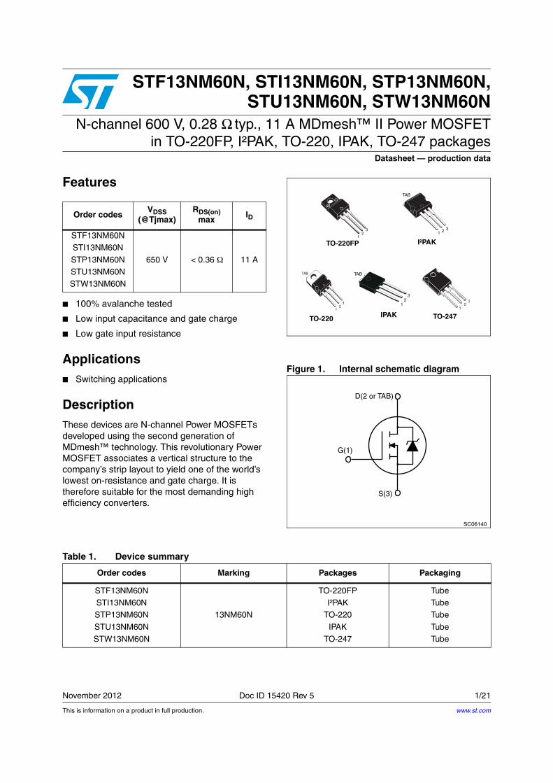
This is information on a product in full production. November 2012 Doc ID 15420 Rev 5 1/21 21 STF13NM60N, STI13NM60N, STP13NM60N, STU13NM60N, STW13NM60N N-channel 600 V, 0.28 Ω typ., 11 A MDmesh™ II Power MOSFET in TO-220FP, I²PAK, TO-220, IPAK, TO-247 packages Datasheet — production data Features ■ 100% avalanche tested ■ Low input capacitance and gate charge ■ Low gate input resistance Applications ■ Switching applications Description These devices are N-channel Power MOSFETs developed using the second generation of MDmesh™ technology. This revolutionary Power MOSFET associates a vertical structure to the company’s strip layout to yield one of the world’s lowest on-resistance and gate charge. It is therefore suitable for the most demanding high efficiency converters. Figure 1. Internal schematic diagram Order codes V DSS (@Tjmax) R DS(on) max I D STF13NM60N STI13NM60N STP13NM60N STU13NM60N STW13NM60N 650 V < 0.36 Ω 11 A TO-220 TO-220FP 1 2 3 TAB 1 2 3 1 2 3 TO-247 1 2 3 I²PAK 3 2 1 IPAK TAB TAB Table 1. Device summary Order codes Marking Packages Packaging STF13NM60N STI13NM60N STP13NM60N STU13NM60N STW13NM60N 13NM60N TO-220FP I²PAK TO-220 IPAK TO-247 Tube Tube Tube Tube Tube www.st.com
Transcript of STF13NM60N, STI13NM60N, STP13NM60N, STU13NM60N, STW13NM60N · 2017-08-08 · STF13NM60N,...
This is information on a product in full production.
November 2012 Doc ID 15420 Rev 5 1/21
21
STF13NM60N, STI13NM60N, STP13NM60N,STU13NM60N, STW13NM60N
N-channel 600 V, 0.28 Ω typ., 11 A MDmesh™ II Power MOSFET in TO-220FP, I²PAK, TO-220, IPAK, TO-247 packages
Datasheet — production data
Features
■ 100% avalanche tested
■ Low input capacitance and gate charge
■ Low gate input resistance
Applications■ Switching applications
DescriptionThese devices are N-channel Power MOSFETs developed using the second generation of MDmesh™ technology. This revolutionary Power MOSFET associates a vertical structure to the company’s strip layout to yield one of the world’s lowest on-resistance and gate charge. It is therefore suitable for the most demanding high efficiency converters.
Figure 1. Internal schematic diagram
Order codesVDSS
(@Tjmax)RDS(on)
maxID
STF13NM60NSTI13NM60N
STP13NM60NSTU13NM60NSTW13NM60N
650 V < 0.36 Ω 11 A
TO-220
TO-220FP
12
3
TAB
12
3
12
3
TO-247
1 2 3
I²PAK
32
1
IPAK
TAB
TAB
Table 1. Device summary
Order codes Marking Packages Packaging
STF13NM60NSTI13NM60NSTP13NM60N
STU13NM60NSTW13NM60N
13NM60N
TO-220FPI²PAK
TO-220
IPAKTO-247
TubeTubeTube
TubeTube
www.st.com
Contents STF/I/P/U/W13NM60N
2/21 Doc ID 15420 Rev 5
Contents
1 Electrical ratings . . . . . . . . . . . . . . . . . . . . . . . . . . . . . . . . . . . . . . . . . . . . 3
2 Electrical characteristics . . . . . . . . . . . . . . . . . . . . . . . . . . . . . . . . . . . . . 4
2.1 Electrical characteristics (curves) . . . . . . . . . . . . . . . . . . . . . . . . . . . . . 6
3 Test circuits . . . . . . . . . . . . . . . . . . . . . . . . . . . . . . . . . . . . . . . . . . . . . . 9
4 Package mechanical data . . . . . . . . . . . . . . . . . . . . . . . . . . . . . . . . . . . . 10
5 Revision history . . . . . . . . . . . . . . . . . . . . . . . . . . . . . . . . . . . . . . . . . . . 20
STF/I/P/U/W13NM60N Electrical ratings
Doc ID 15420 Rev 5 3/21
1 Electrical ratings
Table 2. Absolute maximum ratings
Symbol ParameterValue
UnitTO-220FP I²PAK, TO-220, IPAK, TO-247
VDS Drain-source voltage 600 V
VGS Gate-source voltage ± 25 V
IDDrain current (continuous) at
TC = 25 °C11(1)
1. Limited by maximum junction temperature
11 A
IDDrain current (continuous) at
TC = 100 °C6.93(1) 6.93 A
IDM (2)
2. Pulse width limited by safe operating area
Drain current (pulsed) 44(1) 44 A
PTOT Total dissipation at TC = 25 °C 25 90 W
dv/dt (3)
3. ISD ≤ 11 A, di/dt ≤ 400 A/µs, VDS peak ≤ V(BR)DSS, VDD = 80% V(BR)DSS.
Peak diode recovery voltage slope 15 V/ns
VISO
Insulation withstand voltage (RMS) from all three leads to external heat sink (t=1 s;TC=25 °C)
2500 V
Tstg Storage temperature - 55 to 150 °C
Tj Max. operating junction temperature 150 °C
Table 3. Thermal data
Symbol Parameter
Value
UnitTO-220FP
I²PAK
TO-220IPAK TO-247
Rthj-case Thermal resistance junction-case max 5 1.39 °C/W
Rthj-ambThermal resistance junction-ambient max
62.5 62.5 100 50 °C/W
Table 4. Avalanche characteristics
Symbol Parameter Value Unit
IASAvalanche current, repetitive or not-repetitive (pulse width limited by Tj max)
3.5 A
EASSingle pulse avalanche energy
(starting TJ=25 °C, ID=IAS, VDD=50 V)200 mJ
Electrical characteristics STF/I/P/U/W13NM60N
4/21 Doc ID 15420 Rev 5
2 Electrical characteristics
(TCASE = 25 °C unless otherwise specified)
Table 5. On/off states
Symbol Parameter Test conditions Min. Typ. Max. Unit
V(BR)DSSDrain-source breakdown voltage (VGS = 0)
ID = 1 mA 600 V
IDSSZero gate voltage drain current (VGS = 0)
VDS = 600 VVDS = 600 V, TC=125 °C
1100
µAµA
IGSSGate-body leakagecurrent (VDS = 0)
VGS = ± 25 V ±0.1 µA
VGS(th) Gate threshold voltage VDS = VGS, ID = 250 µA 2 3 4 V
RDS(on)Static drain-source
on-resistanceVGS = 10 V, ID = 5.5 A 0.28 0.36 Ω
Table 6. Dynamic
Symbol Parameter Test conditions Min. Typ. Max. Unit
Ciss
Coss
Crss
Input capacitanceOutput capacitanceReverse transfer capacitance
VDS = 50 V, f = 1 MHz, VGS = 0
-790603.6
-pFpFpF
Coss eq. (1)
1. Coss eq. is defined as a constant equivalent capacitance giving the same charging time as Coss when VDS increases from 0 to 80% VDS
Equivalent output capacitance
VGS = 0, VDS = 0 to 480 V - 135 - pF
Qg
Qgs
Qgd
Total gate chargeGate-source charge
Gate-drain charge
VDD = 480 V, ID = 11 A,VGS = 10 V,
(see Figure 20)
-274
14
-nCnC
nC
RG Gate input resistance f=1 MHz open drain - 4.7 - Ω
STF/I/P/U/W13NM60N Electrical characteristics
Doc ID 15420 Rev 5 5/21
Table 7. Switching times
Symbol Parameter Test conditions Min. Typ. Max. Unit
td(on)
trtd(off)
tf
Turn-on delay time
Rise timeTurn-off delay timeFall time
VDD = 300 V, ID = 5.5 A RG = 4.7 Ω VGS = 10 V
(see Figure 19)-
3
83010
-
ns
nsnsns
Table 8. Source drain diode
Symbol Parameter Test conditions Min Typ. Max. Unit
ISD
ISDM (1)
1. Pulse width limited by safe operating area
Source-drain current
Source-drain current (pulsed)-
11
44
A
A
VSD (2)
2. Pulsed: pulse duration = 300 µs, duty cycle 1.5%
Forward on voltage ISD = 11 A, VGS = 0 - 1.5 V
trrQrr
IRRM
Reverse recovery timeReverse recovery charge
Reverse recovery current
ISD = 11 A, di/dt = 100 A/µsVDD = 100 V
(see Figure 21)
-2302
18
nsµC
A
trrQrr
IRRM
Reverse recovery time
Reverse recovery chargeReverse recovery current
ISD = 11 A, di/dt = 100 A/µs
VDD = 100 V, Tj = 150 °C(see Figure 21)
-
290
19017
ns
µCA
Electrical characteristics STF/I/P/U/W13NM60N
6/21 Doc ID 15420 Rev 5
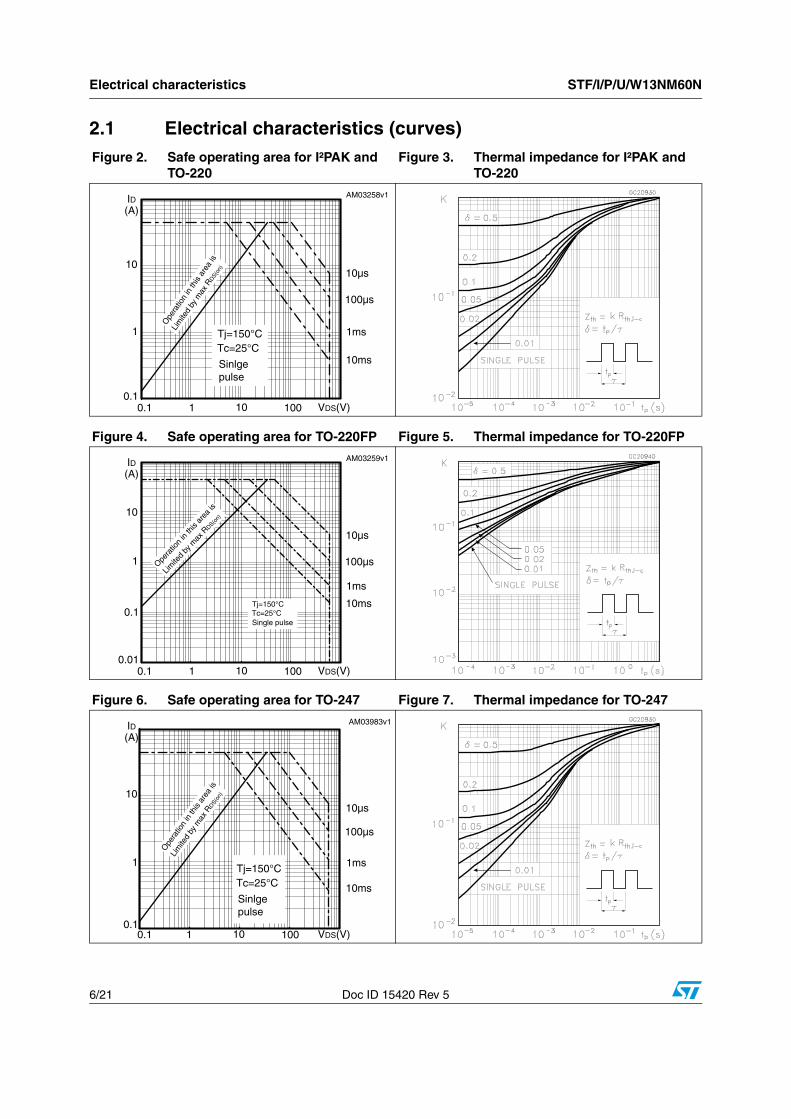
2.1 Electrical characteristics (curves) Figure 2. Safe operating area for I²PAK and
TO-220Figure 3. Thermal impedance for I²PAK and
TO-220
Figure 4. Safe operating area for TO-220FP Figure 5. Thermal impedance for TO-220FP
Figure 6. Safe operating area for TO-247 Figure 7. Thermal impedance for TO-247
ID
10
1
0.10.1 1 100 VDS(V)10
(A)
Ope
ratio
n in
this
are
a is
Lim
ited
by m
ax R
DS(
on)
10µs
100µs
1ms
10ms
Tj=150°CTc=25°C
Sinlgepulse
AM03258v1
ID
10
1
0.1
0.010.1 1 100 VDS(V)10
(A)
Opera
tion
in th
is ar
ea is
Limite
d by
max
RDS(o
n)
10µs
100µs
1ms
10msTj=150°CTc=25°CSingle pulse
AM03259v1
ID
10
1
0.10.1 1 100 VDS(V)10
(A)
Ope
ratio
n in
this
area
is
Lim
ited
by m
ax R
DS(on
)
10µs
100µs
1ms
10ms
Tj=150°CTc=25°C
Sinlgepulse
AM03983v1
STF/I/P/U/W13NM60N Electrical characteristics
Doc ID 15420 Rev 5 7/21
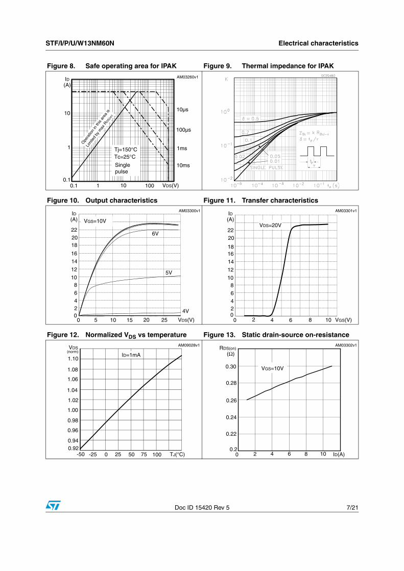
Figure 8. Safe operating area for IPAK Figure 9. Thermal impedance for IPAK
Figure 10. Output characteristics Figure 11. Transfer characteristics
Figure 12. Normalized VDS vs temperature Figure 13. Static drain-source on-resistance
VDS
-50 0 TJ(°C)
(norm)
-25 7525 50 1000.920.94
0.96
0.98
1.00
1.02
1.04
1.06
ID=1mA
1.08
1.10
AM09028v1RDS(on)
0.26
0.24
0.22
0.20 4 ID(A)
(Ω)
2 6
0.28
0.30 VGS=10V
8 10
AM03302v1
Electrical characteristics STF/I/P/U/W13NM60N
8/21 Doc ID 15420 Rev 5
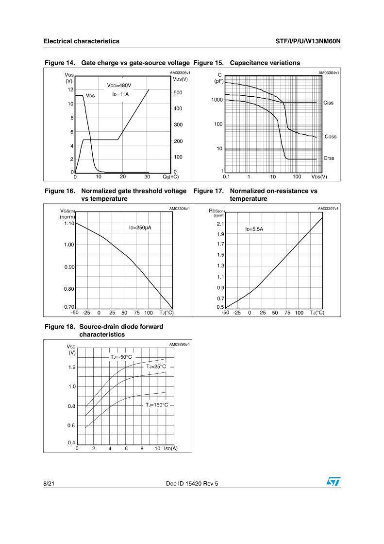
Figure 14. Gate charge vs gate-source voltage Figure 15. Capacitance variations
Figure 16. Normalized gate threshold voltage vs temperature
Figure 17. Normalized on-resistance vs temperature
Figure 18. Source-drain diode forward characteristics
VGS
6
4
2
00 Qg(nC)
(V)
20
8
10
10
VDD=480V
ID=11A
30
12
300
200
100
0
400
500VDS
VDS(V)
AM03305v1
VGS(th)
1.00
0.90
0.80
0.70-50 0 TJ(°C)
(norm)
-25
1.10
7525 50 100
ID=250µA
AM03306v1 RDS(on)
1.1
0.9
0.7
0.5-50 0 TJ(°C)
(norm)
-25 7525 50 100
1.7
1.5
1.3
1.9
2.1ID=5.5A
AM03307v1
VSD
0 4 ISD(A)
(V)
2 106 80.4
0.6
0.8
1.0
1.2
TJ=-50°C
TJ=25°C
TJ=150°C
AM09290v1
STF/I/P/U/W13NM60N Test circuits
Doc ID 15420 Rev 5 9/21
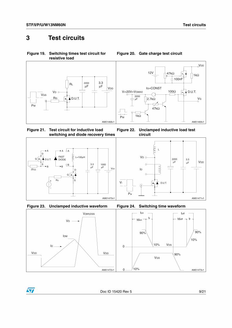
3 Test circuits
Figure 19. Switching times test circuit for resistive load
Figure 20. Gate charge test circuit
Figure 21. Test circuit for inductive load switching and diode recovery times
Figure 22. Unclamped inductive load test circuit
Figure 23. Unclamped inductive waveform Figure 24. Switching time waveform
AM01468v1
VGS
PW
VD
RG
RL
D.U.T.
2200
μF3.3μF
VDD
AM01469v1
VDD
47kΩ 1kΩ
47kΩ
2.7kΩ
1kΩ
12V
Vi=20V=VGMAX
2200μF
PW
IG=CONST100Ω
100nF
D.U.T.
VG
AM01470v1
AD
D.U.T.
SB
G
25 Ω
A A
BB
RG
G
FASTDIODE
D
S
L=100μH
μF3.3 1000
μF VDD
AM01471v1
Vi
Pw
VD
ID
D.U.T.
L
2200μF
3.3μF VDD
AM01472v1
V(BR)DSS
VDDVDD
VD
IDM
ID
AM01473v1
VDS
ton
tdon tdoff
toff
tftr
90%
10%
10%
0
0
90%
90%
10%
VGS
Package mechanical data STF/I/P/U/W13NM60N
10/21 Doc ID 15420 Rev 5
4 Package mechanical data
In order to meet environmental requirements, ST offers these devices in different grades of ECOPACK® packages, depending on their level of environmental compliance. ECOPACK® specifications, grade definitions and product status are available at: www.st.com. ECOPACK is an ST trademark.
STF/I/P/U/W13NM60N Package mechanical data
Doc ID 15420 Rev 5 11/21
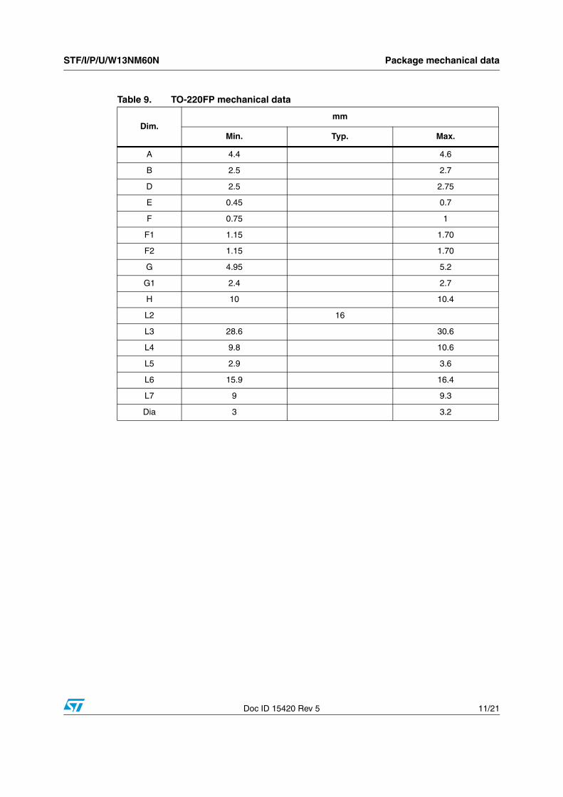
Table 9. TO-220FP mechanical data
Dim.mm
Min. Typ. Max.
A 4.4 4.6
B 2.5 2.7
D 2.5 2.75
E 0.45 0.7
F 0.75 1
F1 1.15 1.70
F2 1.15 1.70
G 4.95 5.2
G1 2.4 2.7
H 10 10.4
L2 16
L3 28.6 30.6
L4 9.8 10.6
L5 2.9 3.6
L6 15.9 16.4
L7 9 9.3
Dia 3 3.2
Package mechanical data STF/I/P/U/W13NM60N
12/21 Doc ID 15420 Rev 5
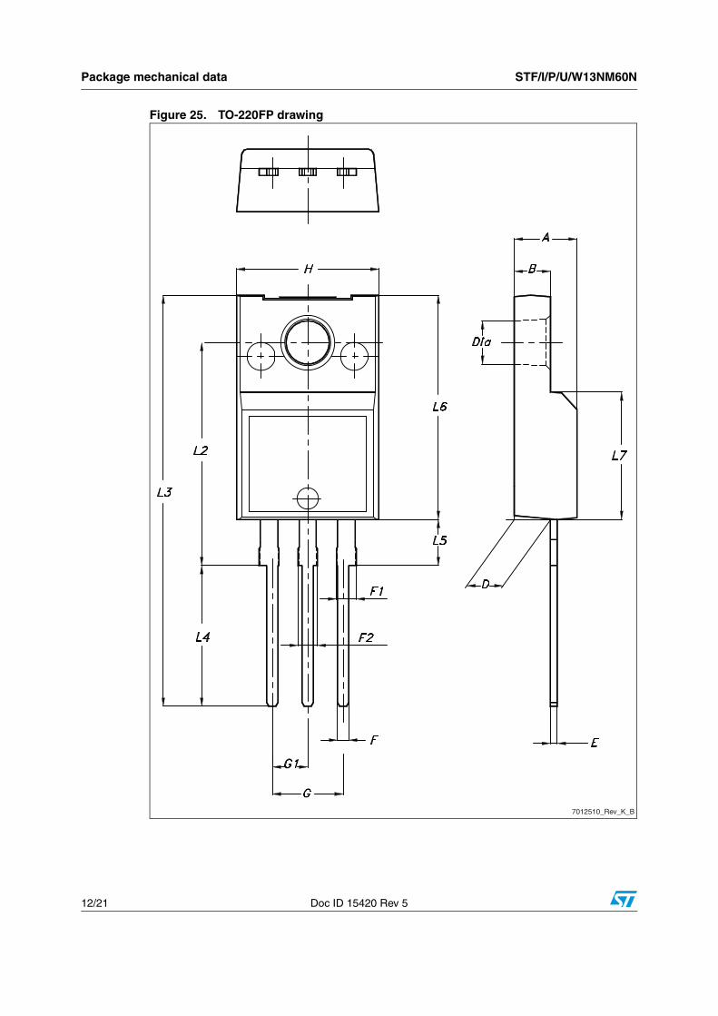
Figure 25. TO-220FP drawing
7012510_Rev_K_B
STF/I/P/U/W13NM60N Package mechanical data
Doc ID 15420 Rev 5 13/21
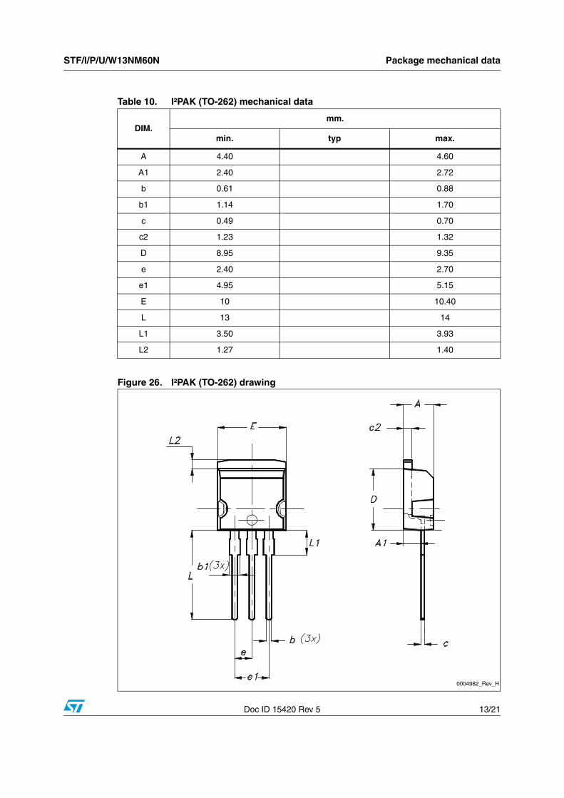
Figure 26. I²PAK (TO-262) drawing
Table 10. I²PAK (TO-262) mechanical data
DIM.mm.
min. typ max.
A 4.40 4.60
A1 2.40 2.72
b 0.61 0.88
b1 1.14 1.70
c 0.49 0.70
c2 1.23 1.32
D 8.95 9.35
e 2.40 2.70
e1 4.95 5.15
E 10 10.40
L 13 14
L1 3.50 3.93
L2 1.27 1.40
0004982_Rev_H
Package mechanical data STF/I/P/U/W13NM60N
14/21 Doc ID 15420 Rev 5
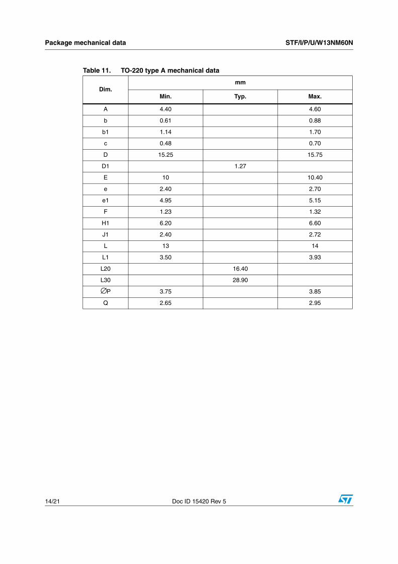
Table 11. TO-220 type A mechanical data
Dim.mm
Min. Typ. Max.
A 4.40 4.60
b 0.61 0.88
b1 1.14 1.70
c 0.48 0.70
D 15.25 15.75
D1 1.27
E 10 10.40
e 2.40 2.70
e1 4.95 5.15
F 1.23 1.32
H1 6.20 6.60
J1 2.40 2.72
L 13 14
L1 3.50 3.93
L20 16.40
L30 28.90
∅P 3.75 3.85
Q 2.65 2.95
STF/I/P/U/W13NM60N Package mechanical data
Doc ID 15420 Rev 5 15/21
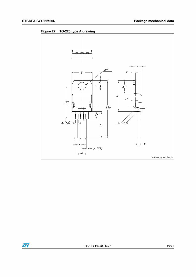
Figure 27. TO-220 type A drawing
0015988_typeA_Rev_S
Package mechanical data STF/I/P/U/W13NM60N
16/21 Doc ID 15420 Rev 5
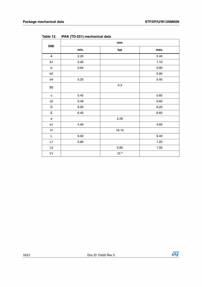
Table 12. IPAK (TO-251) mechanical data
DIM.mm.
min. typ max.
A 2.20 2.40
A1 0.90 1.10
b 0.64 0.90
b2 0.95
b4 5.20 5.40
B50.3
c 0.45 0.60
c2 0.48 0.60
D 6.00 6.20
E 6.40 6.60
e 2.28
e1 4.40 4.60
H 16.10
L 9.00 9.40
L1 0.80 1.20
L2 0.80 1.00
V1 10 o
STF/I/P/U/W13NM60N Package mechanical data
Doc ID 15420 Rev 5 17/21
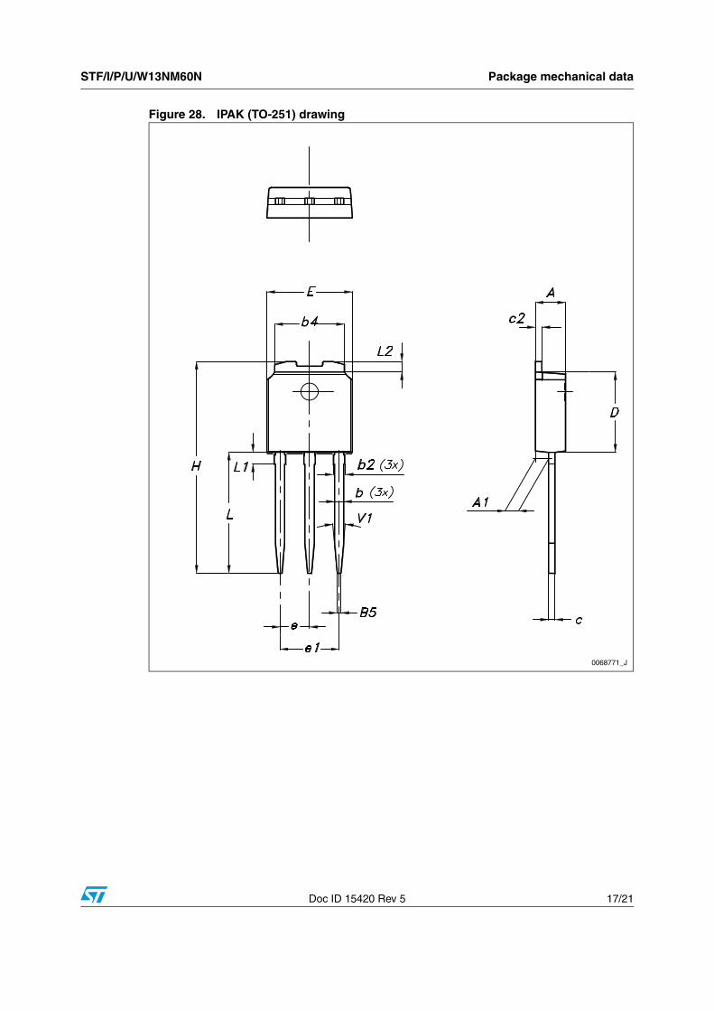
Figure 28. IPAK (TO-251) drawing
0068771_J
Package mechanical data STF/I/P/U/W13NM60N
18/21 Doc ID 15420 Rev 5
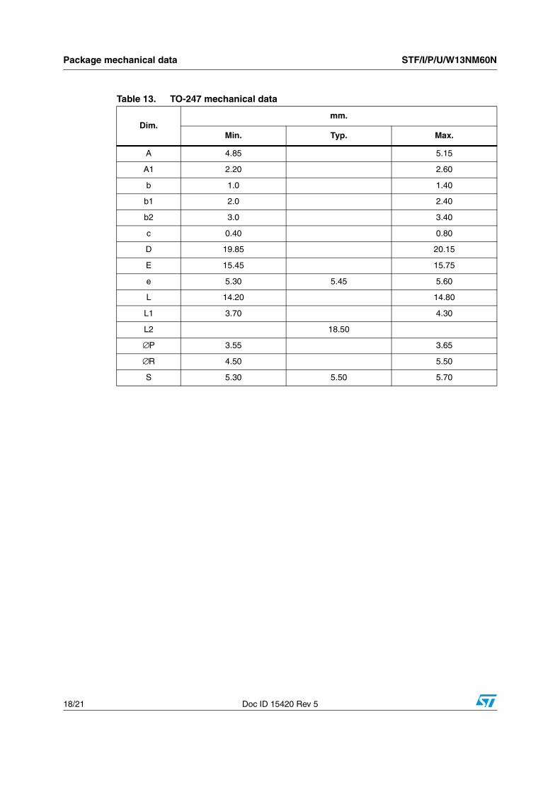
Table 13. TO-247 mechanical data
Dim.mm.
Min. Typ. Max.
A 4.85 5.15
A1 2.20 2.60
b 1.0 1.40
b1 2.0 2.40
b2 3.0 3.40
c 0.40 0.80
D 19.85 20.15
E 15.45 15.75
e 5.30 5.45 5.60
L 14.20 14.80
L1 3.70 4.30
L2 18.50
∅P 3.55 3.65
∅R 4.50 5.50
S 5.30 5.50 5.70
STF/I/P/U/W13NM60N Package mechanical data
Doc ID 15420 Rev 5 19/21
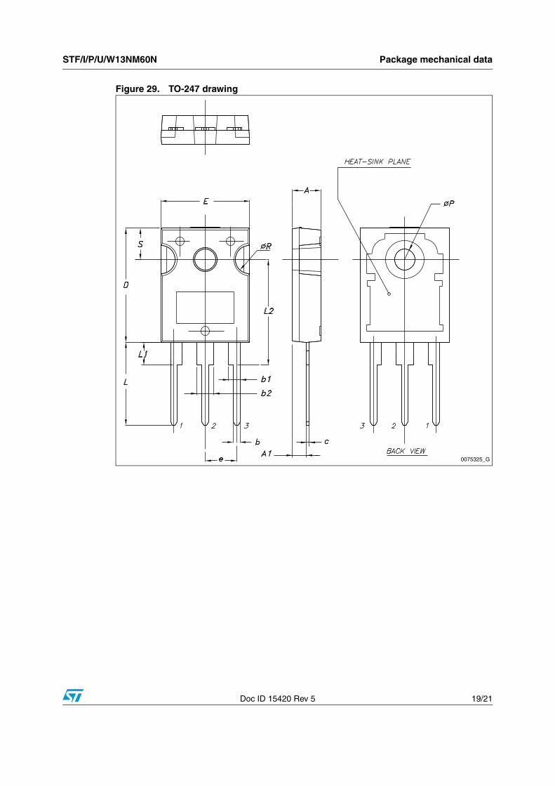
Figure 29. TO-247 drawing
0075325_G
Revision history STF/I/P/U/W13NM60N
20/21 Doc ID 15420 Rev 5
5 Revision history
Table 14. Document revision history
Date Revision Changes
29-Feb-2009 1 First release
13-Jan-2010 2– Added new package, mechanical data: TO-247– Added new package, mechanical data: D²PAK
08-Nov-2010 3– Modified Figure 4– Added new package, mechanical data: I²PAK
18-Jan-2012 4– Added new package, mechanical data: IPAK– Minor text changes
14-Nov-2012 5The part numbers STB13NM60N and STD13NM60N have been moved to a separate datasheet.
Section 4: Package mechanical data has been updated.
STF/I/P/U/W13NM60N
Doc ID 15420 Rev 5 21/21
Please Read Carefully:
Information in this document is provided solely in connection with ST products. STMicroelectronics NV and its subsidiaries (“ST”) reserve theright to make changes, corrections, modifications or improvements, to this document, and the products and services described herein at anytime, without notice.
All ST products are sold pursuant to ST’s terms and conditions of sale.
Purchasers are solely responsible for the choice, selection and use of the ST products and services described herein, and ST assumes noliability whatsoever relating to the choice, selection or use of the ST products and services described herein.
No license, express or implied, by estoppel or otherwise, to any intellectual property rights is granted under this document. If any part of thisdocument refers to any third party products or services it shall not be deemed a license grant by ST for the use of such third party productsor services, or any intellectual property contained therein or considered as a warranty covering the use in any manner whatsoever of suchthird party products or services or any intellectual property contained therein.
UNLESS OTHERWISE SET FORTH IN ST’S TERMS AND CONDITIONS OF SALE ST DISCLAIMS ANY EXPRESS OR IMPLIEDWARRANTY WITH RESPECT TO THE USE AND/OR SALE OF ST PRODUCTS INCLUDING WITHOUT LIMITATION IMPLIEDWARRANTIES OF MERCHANTABILITY, FITNESS FOR A PARTICULAR PURPOSE (AND THEIR EQUIVALENTS UNDER THE LAWSOF ANY JURISDICTION), OR INFRINGEMENT OF ANY PATENT, COPYRIGHT OR OTHER INTELLECTUAL PROPERTY RIGHT.
UNLESS EXPRESSLY APPROVED IN WRITING BY TWO AUTHORIZED ST REPRESENTATIVES, ST PRODUCTS ARE NOTRECOMMENDED, AUTHORIZED OR WARRANTED FOR USE IN MILITARY, AIR CRAFT, SPACE, LIFE SAVING, OR LIFE SUSTAININGAPPLICATIONS, NOR IN PRODUCTS OR SYSTEMS WHERE FAILURE OR MALFUNCTION MAY RESULT IN PERSONAL INJURY,DEATH, OR SEVERE PROPERTY OR ENVIRONMENTAL DAMAGE. ST PRODUCTS WHICH ARE NOT SPECIFIED AS "AUTOMOTIVEGRADE" MAY ONLY BE USED IN AUTOMOTIVE APPLICATIONS AT USER’S OWN RISK.
Resale of ST products with provisions different from the statements and/or technical features set forth in this document shall immediately voidany warranty granted by ST for the ST product or service described herein and shall not create or extend in any manner whatsoever, anyliability of ST.
ST and the ST logo are trademarks or registered trademarks of ST in various countries.
Information in this document supersedes and replaces all information previously supplied.
The ST logo is a registered trademark of STMicroelectronics. All other names are the property of their respective owners.
© 2012 STMicroelectronics - All rights reserved
STMicroelectronics group of companies
Australia - Belgium - Brazil - Canada - China - Czech Republic - Finland - France - Germany - Hong Kong - India - Israel - Italy - Japan - Malaysia - Malta - Morocco - Philippines - Singapore - Spain - Sweden - Switzerland - United Kingdom - United States of America
www.st.com