STD1NK60 - STD1NK60-1 STQ1HNK60Rmedia.digikey.com/PDF/Data Sheets/ST Microelectronics... ·...
13
1/13 June 2003 STD1NK60 - STD1NK60-1 STQ1HNK60R N-CHANNEL 600V - 8Ω - 1A DPAK / IPAK / TO-92 SuperMESH™Power MOSFET ■ TYPICAL R DS (on) = 8 Ω ■ EXTREMELY HIGH dv/dt CAPABILITY ■ 100% AVALANCHE TESTED ■ GATE CHARGE MINIMIZED ■ NEW HIGH VOLTAGE BENCHMARK DESCRIPTION The SuperMESH™ series is obtained through an extreme optimization of ST’s well established strip- based PowerMESH™ layout. In addition to pushing on-resistance significantly down, special care is tak- en to ensure a very good dv/dt capability for the most demanding applications. Such series comple- ments ST full range of high voltage MOSFETs in- cluding revolutionary MDmesh™ products. APPLICATIONS ■ SWITCH MODE LOW POWER SUPPLIES (SMPS) ■ LOW POWER, LOW COST CFL (COMPACT FLUORESCENT LAMPS) ■ LOW POWER BATTERY CHARGERS ORDERING INFORMATION TYPE V DSS R DS(on) I D Pw STD1NK60 STD1NK60-1 STQ1HNK60R 600 V 600 V 600 V < 8.5 Ω < 8.5 Ω < 8.5 Ω 1A 1A 0.4 A 30 W 30 W 3W SALES TYPE MARKING PACKAGE PACKAGING STD1NK60T4 D1NK60 DPAK TAPE & REEL STD1NK60-1 D1NK60 IPAK TUBE STQ1HNK60R 1HNK60R TO-92 BULK STQ1HNK60R-AP 1HNK60R TO-92 AMMOPAK IPAK 3 2 1 TO-92 TO-92 (Ammopack) 1 3 DPAK INTERNAL SCHEMATIC DIAGRAM
Transcript of STD1NK60 - STD1NK60-1 STQ1HNK60Rmedia.digikey.com/PDF/Data Sheets/ST Microelectronics... ·...

1/13June 2003
STD1NK60 - STD1NK60-1STQ1HNK60R
N-CHANNEL 600V - 8Ω - 1A DPAK / IPAK / TO-92SuperMESH™Power MOSFET
TYPICAL RDS(on) = 8 Ω EXTREMELY HIGH dv/dt CAPABILITY 100% AVALANCHE TESTED GATE CHARGE MINIMIZED NEW HIGH VOLTAGE BENCHMARK
DESCRIPTIONThe SuperMESH™ series is obtained through anextreme optimization of ST’s well established strip-based PowerMESH™ layout. In addition to pushingon-resistance significantly down, special care is tak-en to ensure a very good dv/dt capability for themost demanding applications. Such series comple-ments ST full range of high voltage MOSFETs in-cluding revolutionary MDmesh™ products.
APPLICATIONS SWITCH MODE LOW POWER SUPPLIES
(SMPS) LOW POWER, LOW COST CFL (COMPACT
FLUORESCENT LAMPS) LOW POWER BATTERY CHARGERS
ORDERING INFORMATION
TYPE VDSS RDS(on) ID Pw
STD1NK60STD1NK60-1STQ1HNK60R
600 V600 V600 V
< 8.5 Ω< 8.5 Ω< 8.5 Ω
1 A1 A
0.4 A
30 W30 W3 W
SALES TYPE MARKING PACKAGE PACKAGING
STD1NK60T4 D1NK60 DPAK TAPE & REEL
STD1NK60-1 D1NK60 IPAK TUBE
STQ1HNK60R 1HNK60R TO-92 BULK
STQ1HNK60R-AP 1HNK60R TO-92 AMMOPAK
IPAK
32
1
TO-92TO-92 (Ammopack)
1
3
DPAK
INTERNAL SCHEMATIC DIAGRAM
STD1NK60 - STD1NK60-1 - STQ1HNK60R
2/13
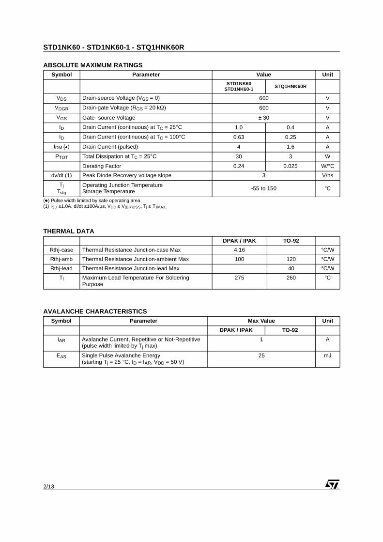
ABSOLUTE MAXIMUM RATINGS
() Pulse width limited by safe operating area(1) ISD ≤1.0A, di/dt ≤100A/µs, VDD ≤ V(BR)DSS, Tj ≤ TJMAX.
THERMAL DATA
AVALANCHE CHARACTERISTICS
Symbol Parameter Value Unit
STD1NK60STD1NK60-1 STQ1HNK60R
VDS Drain-source Voltage (VGS = 0) 600 V
VDGR Drain-gate Voltage (RGS = 20 kΩ) 600 V
VGS Gate- source Voltage ± 30 V
ID Drain Current (continuous) at TC = 25°C 1.0 0.4 A
ID Drain Current (continuous) at TC = 100°C 0.63 0.25 A
IDM () Drain Current (pulsed) 4 1.6 A
PTOT Total Dissipation at TC = 25°C 30 3 W
Derating Factor 0.24 0.025 W/°C
dv/dt (1) Peak Diode Recovery voltage slope 3 V/ns
TjTstg
Operating Junction TemperatureStorage Temperature -55 to 150 °C
DPAK / IPAK TO-92
Rthj-case Thermal Resistance Junction-case Max 4.16 °C/W
Rthj-amb Thermal Resistance Junction-ambient Max 100 120 °C/W
Rthj-lead Thermal Resistance Junction-lead Max 40 °C/W
Tl Maximum Lead Temperature For SolderingPurpose
275 260 °C
Symbol Parameter Max Value Unit
DPAK / IPAK TO-92
IAR Avalanche Current, Repetitive or Not-Repetitive(pulse width limited by Tj max)
1 A
EAS Single Pulse Avalanche Energy(starting Tj = 25 °C, ID = IAR, VDD = 50 V)
25 mJ

3/13
STD1NK60 - STD1NK60-1 - STQ1HNK60R
ELECTRICAL CHARACTERISTICS (TCASE =25°C UNLESS OTHERWISE SPECIFIED)ON/OFF
DYNAMIC
SWITCHING ON
SWITCHING OFF
SOURCE DRAIN DIODE
Note: 1. Pulsed: Pulse duration = 300 µs, duty cycle 1.5 %.2. Pulse width limited by safe operating area.
Symbol Parameter Test Conditions Min. Typ. Max. Unit
V(BR)DSS Drain-sourceBreakdown Voltage
ID = 1 mA, VGS = 0 600 V
IDSS Zero Gate VoltageDrain Current (VGS = 0)
VDS = Max RatingVDS = Max Rating, TC = 125 °C
150
µAµA
IGSS Gate-body LeakageCurrent (VDS = 0)
VGS = ± 30V ±100 nA
VGS(th) Gate Threshold Voltage VDS = VGS, ID = 250µA 2.25 3 3.7 V
RDS(on) Static Drain-source OnResistance
VGS = 10V, ID = 0.5 A 8 8.5 Ω
Symbol Parameter Test Conditions Min. Typ. Max. Unit
gfs (1) Forward Transconductance VDS > ID(on) x RDS(on)max,ID = 0.5 A
1 S
CissCossCrss
Input CapacitanceOutput CapacitanceReverse TransferCapacitance
VDS = 25V, f = 1 MHz, VGS = 0 15623.53.8
pFpFpF
Symbol Parameter Test Conditions Min. Typ. Max. Unit
td(on)tr
Turn-on Delay TimeRise Time
VDD = 300 V, ID = 0.5 ARG = 4.7Ω VGS = 10 V(Resistive Load see, Figure 3)
6.55
nsns
QgQgsQgd
Total Gate ChargeGate-Source ChargeGate-Drain Charge
VDD = 480V, ID = 1.0 A,VGS = 10V, RG = 4.7Ω
71.13.4
10 nCnCnC
Symbol Parameter Test Conditions Min. Typ. Max. Unit
td(off)tf
Turn-off Delay TimeFall Time
VDD = 300 V, ID = 0.5 ARG = 4.7Ω VGS = 10 V(Resistive Load see, Figure 3)
1925
nsns
tr(Voff)tftc
Off-voltage Rise TimeFall TimeCross-over Time
VDD = 480V, ID = 1.0 A,RG = 4.7Ω, VGS = 10V(Inductive Load see, Figure 5)
242544
nsnsns
Symbol Parameter Test Conditions Min. Typ. Max. Unit
ISDISDM (2)
Source-drain CurrentSource-drain Current (pulsed)
14
AA
VSD (1) Forward On Voltage ISD = 1.0 A, VGS = 0 1.6 V
trrQrr
IRRM
Reverse Recovery TimeReverse Recovery ChargeReverse Recovery Current
ISD = 1.0 A, di/dt = 100A/µsVDD = 25V, Tj = 150°C(see test circuit, Figure 5)
2293773.3
nsµCA

STD1NK60 - STD1NK60-1 - STQ1HNK60R
4/13
Thermal Impedance For TO-92
Thermal Impedance For DPAK/IPAKSafe Operating Area For DPAK/IPAK
Safe Operating Area For TO-92
Output Characteristics Transfer Characteristics

5/13
STD1NK60 - STD1NK60-1 - STQ1HNK60R
Normalized On Resistance vs TemperatureNormalized Gate Threshold Voltage vs Temp.
Static Drain-source On ResistanceTransconductance
Gate Charge vs Gate-source Voltage Capacitance Variations
STD1NK60 - STD1NK60-1 - STQ1HNK60R
6/13
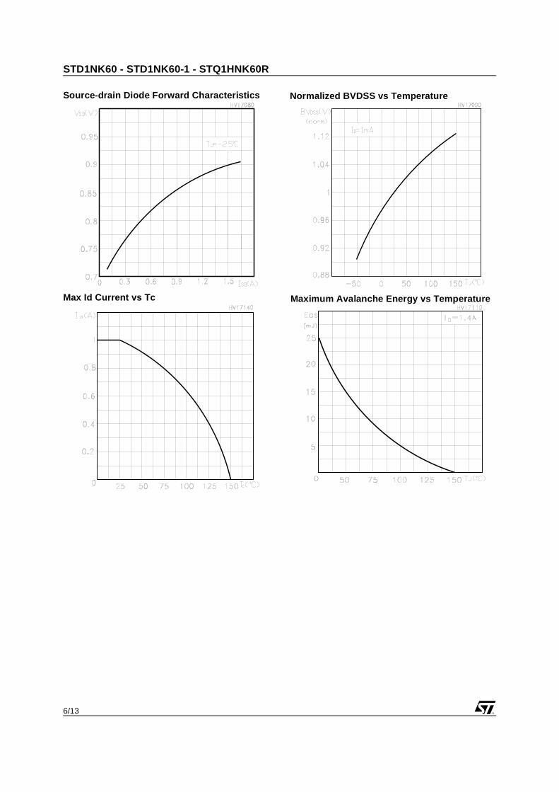
Normalized BVDSS vs TemperatureSource-drain Diode Forward Characteristics
Max Id Current vs Tc Maximum Avalanche Energy vs Temperature

7/13
STD1NK60 - STD1NK60-1 - STQ1HNK60R
Fig. 5: Test Circuit For Inductive Load SwitchingAnd Diode Recovery Times
Fig. 4: Gate Charge test Circuit
Fig. 2: Unclamped Inductive WaveformFig. 1: Unclamped Inductive Load Test Circuit
Fig. 3: Switching Times Test Circuit ForResistive Load
STD1NK60 - STD1NK60-1 - STQ1HNK60R
8/13
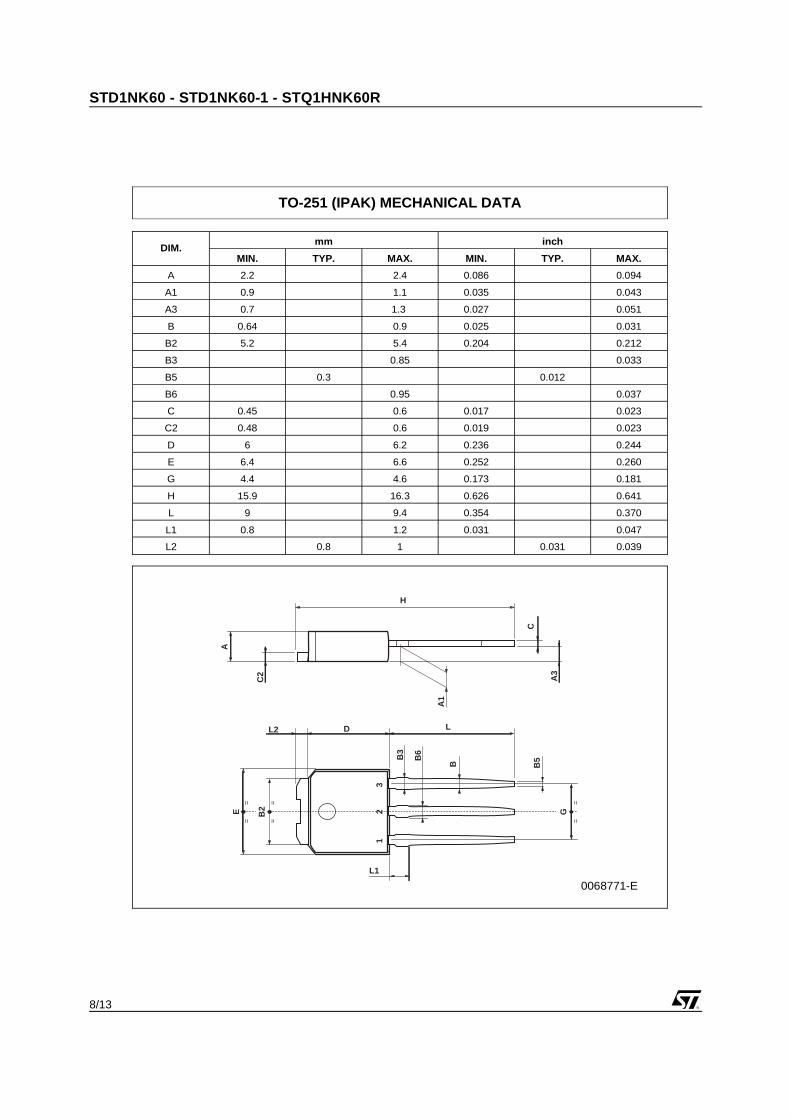
DIM.mm inch
MIN. TYP. MAX. MIN. TYP. MAX.
A 2.2 2.4 0.086 0.094
A1 0.9 1.1 0.035 0.043
A3 0.7 1.3 0.027 0.051
B 0.64 0.9 0.025 0.031
B2 5.2 5.4 0.204 0.212
B3 0.85 0.033
B5 0.3 0.012
B6 0.95 0.037
C 0.45 0.6 0.017 0.023
C2 0.48 0.6 0.019 0.023
D 6 6.2 0.236 0.244
E 6.4 6.6 0.252 0.260
G 4.4 4.6 0.173 0.181
H 15.9 16.3 0.626 0.641
L 9 9.4 0.354 0.370
L1 0.8 1.2 0.031 0.047
L2 0.8 1 0.031 0.039
A
C2
C
A3
H
A1
D LL2
L1
1 3
=
=
B3
B B
6
B2 E
G
=
=
=
=
B5
2
TO-251 (IPAK) MECHANICAL DATA
0068771-E

9/13
STD1NK60 - STD1NK60-1 - STQ1HNK60R
DIM.mm inch
MIN. TYP. MAX. MIN. TYP. MAX.
A 2.20 2.40 0.087 0.094
A1 0.90 1.10 0.035 0.043
A2 0.03 0.23 0.001 0.009
B 0.64 0.90 0.025 0.035
B2 5.20 5.40 0.204 0.213
C 0.45 0.60 0.018 0.024
C2 0.48 0.60 0.019 0.024
D 6.00 6.20 0.236 0.244
E 6.40 6.60 0.252 0.260
G 4.40 4.60 0.173 0.181
H 9.35 10.10 0.368 0.398
L2 0.8 0.031
L4 0.60 1.00 0.024 0.039
V2 0o 8o 0o 0o
P032P_B
TO-252 (DPAK) MECHANICAL DATA

STD1NK60 - STD1NK60-1 - STQ1HNK60R
10/13
DIM.mm. inch
MIN. TYP MAX. MIN. TYP. MAX.
A 4.32 4.95 0.170 0.194
b 0.36 0.51 0.014 0.020
D 4.45 4.95 0.175 0.194
E 3.30 3.94 0.130 0.155
e 2.41 2.67 0.094 0.105
e1 1.14 1.40 0.044 0.055
L 12.70 15.49 0.50 0.610
R 2.16 2.41 0.085 0.094
S1 0.92 1.52 0.036 0.060
W 0.41 0.56 0.016 0.022
V 5° 5°
TO-92 MECHANICAL DATA
11/13
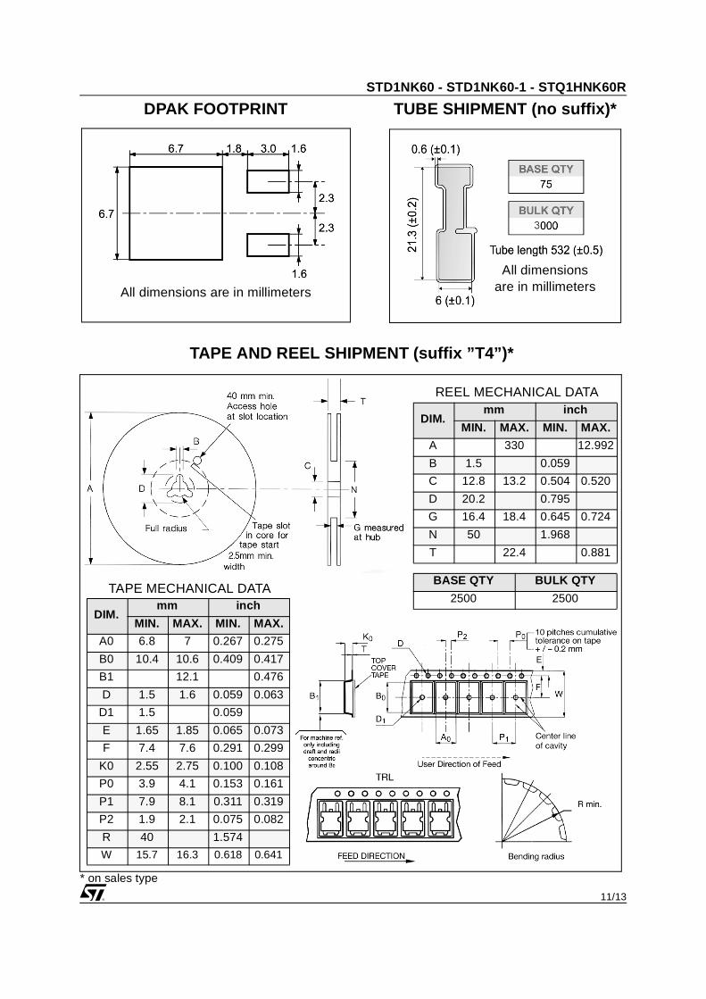
STD1NK60 - STD1NK60-1 - STQ1HNK60R
TAPE AND REEL SHIPMENT (suffix ”T4”)*
TUBE SHIPMENT (no suffix)*DPAK FOOTPRINT
* on sales type
DIM.mm inch
MIN. MAX. MIN. MAX.
A 330 12.992
B 1.5 0.059
C 12.8 13.2 0.504 0.520
D 20.2 0.795
G 16.4 18.4 0.645 0.724
N 50 1.968
T 22.4 0.881
BASE QTY BULK QTY
2500 2500
REEL MECHANICAL DATA
DIM.mm inch
MIN. MAX. MIN. MAX.
A0 6.8 7 0.267 0.275
B0 10.4 10.6 0.409 0.417
B1 12.1 0.476
D 1.5 1.6 0.059 0.063
D1 1.5 0.059
E 1.65 1.85 0.065 0.073
F 7.4 7.6 0.291 0.299
K0 2.55 2.75 0.100 0.108
P0 3.9 4.1 0.153 0.161
P1 7.9 8.1 0.311 0.319
P2 1.9 2.1 0.075 0.082
R 40 1.574
W 15.7 16.3 0.618 0.641
TAPE MECHANICAL DATA
All dimensionsare in millimetersAll dimensions are in millimeters
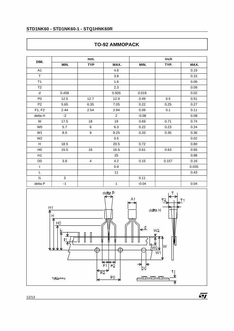
STD1NK60 - STD1NK60-1 - STQ1HNK60R
12/13
DIM.mm. inch
MIN. TYP MAX. MIN. TYP. MAX.
A1 4.8 0.19
T 3.8 0.15
T1 1.6 0.06
T2 2.3 0.09
d 0.458 0.505 0.018 0.02
P0 12.5 12.7 12.9 0.49 0.5 0.51
P2 5.65 6.35 7.05 0.22 0.25 0.27
F1, F2 2.44 2.54 2.94 0.09 0.1 0.11
delta H -2 2 -0.08 0.08
W 17.5 18 19 0.69 0.71 0.74
W0 5.7 6 6.3 0.22 0.23 0.24
W1 8.5 9 9.25 0.33 0.35 0.36
W2 0.5 0.02
H 18.5 20.5 0.72 0.80
H0 15.5 16 16.5 0.61 0.63 0.65
H1 25 0.98
D0 3.8 4 4.2 0.15 0.157 0.16
t 0.9 0.035
L 11 0.43
l1 3 0.11
delta P -1 1 -0.04 0.04
TO-92 AMMOPACK

13/13
STD1NK60 - STD1NK60-1 - STQ1HNK60R
Information furnished is believed to be accurate and reliable. However, STMicroelectronics assumes no responsibility for theconsequences of use of such information nor for any infringement of patents or other rights of third parties which may result f romits use. No license is granted by implication or otherwise under any patent or patent rights of STMicroelectronics. Specificati onsmentioned in this publication are subject to change without notice. This publication supersedes and replaces all informationpreviously supplied. STMicroelectronics products are not authorized for use as critical components in life support devices orsystems without express written approval of STMicroelectronics.
© The ST logo is a registered trademark of STMicroelectronics
© 2003 STMicroelectronics - Printed in Italy - All Rights ReservedSTMicroelectronics GROUP OF COMPANIES
Australia - Brazil - Canada - China - Finland - France - Germany - Hong Kong - India - Israel - Italy - Japan - Malaysia - Malta - Morocco Singapore - Spain - Sweden - Switzerland - United Kingdom - United States.
© http://www.st.com

![arXiv:1111.0965v1 [cs.DS] 3 Nov 2011people.eecs.berkeley.edu/~prasad/Files/highercheeger.pdf · i is the ith smallest eigenvalue of the normalized Laplacian and c0 are](https://static.fdocument.org/doc/165x107/5f7025cbc2e59c51ca4fa3a2/arxiv11110965v1-csds-3-nov-prasadfileshighercheegerpdf-i-is-the-ith-smallest.jpg)


![Index [luthuli.cs.uiuc.edu]luthuli.cs.uiuc.edu/~daf/CV2E-site/indexalgs.pdfINDEX 740 divisive, 281–283 normalized cuts, 284, 285 group average clustering, 270 grouping and agglomeration,](https://static.fdocument.org/doc/165x107/5f3da939408c571e2576f9ce/index-dafcv2e-siteindexalgspdf-index-740-divisive-281a283-normalized-cuts.jpg)