SP331 Data Sheet - exar.com · RX4 15K Ω 400KΩ Vcc 400KΩ Vcc ...
13
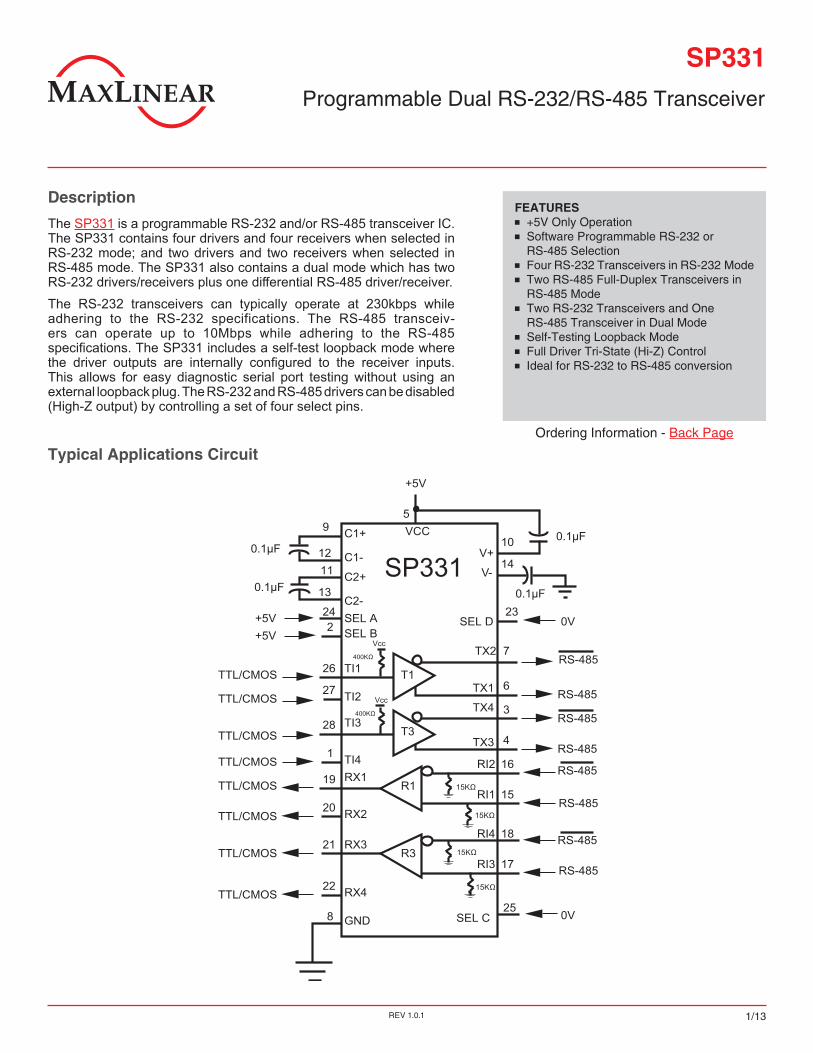
Programmable Dual RS-232/RS-485 Transceiver SP331 1/13 REV 1.0.1 FEATURES ■ ■ +5V Only Operation ■ ■ Software Programmable RS-232 or RS-485 Selection ■ ■ Four RS-232 Transceivers in RS-232 Mode ■ ■ Two RS-485 Full-Duplex Transceivers in RS-485 Mode ■ ■ Two RS-232 Transceivers and One RS-485 Transceiver in Dual Mode ■ ■ Self-Testing Loopback Mode ■ ■ Full Driver Tri-State (Hi-Z) Control ■ ■ Ideal for RS-232 to RS-485 conversion Description The SP331 is a programmable RS-232 and/or RS-485 transceiver IC. The SP331 contains four drivers and four receivers when selected in RS-232 mode; and two drivers and two receivers when selected in RS-485 mode. The SP331 also contains a dual mode which has two RS-232 drivers/receivers plus one differential RS-485 driver/receiver. The RS-232 transceivers can typically operate at 230kbps while adhering to the RS-232 specifications. The RS-485 transceiv- ers can operate up to 10Mbps while adhering to the RS-485 specifications. The SP331 includes a self-test loopback mode where the driver outputs are internally configured to the receiver inputs. This allows for easy diagnostic serial port testing without using an external loopback plug. The RS-232 and RS-485 drivers can be disabled (High-Z output) by controlling a set of four select pins. Typical Applications Circuit Ordering Information - Back Page SEL A TTL/CMOS TTL/CMOS TTL/CMOS 0.1μF C1+ C1- C2+ C2- 1 SEL B 2 +5V VCC 5 GND 8 9 11 12 13 19 20 22 24 26 27 28 TTL/CMOS TTL/CMOS TTL/CMOS TTL/CMOS T1 T3 R1 RS-485 RS-485 RS-485 0V V+ V- 0V SEL C RS-485 RS-485 RS-485 4 6 7 10 14 15 16 23 25 3 RI1 RI2 TX3 TX4 TX1 TX2 TI1 TI2 TI3 TI4 RX1 RX2 TTL/CMOS 21 R3 17 18 RI4 RI3 RX3 RX4 15KΩ 400KΩ Vcc 400KΩ Vcc SEL D RS-485 RS-485 +5V +5V SP331 15KΩ 15KΩ 15KΩ 0.1μF 0.1μF 0.1μF
Transcript of SP331 Data Sheet - exar.com · RX4 15K Ω 400KΩ Vcc 400KΩ Vcc ...
Programmable Dual RS-232/RS-485 Transceiver
SP331
1/13REV 1.0.1
FEATURES +5V Only Operation Software Programmable RS-232 or
RS-485 Selection Four RS-232 Transceivers in RS-232 Mode Two RS-485 Full-Duplex Transceivers in
RS-485 Mode Two RS-232 Transceivers and One
RS-485 Transceiver in Dual Mode Self-Testing Loopback Mode Full Driver Tri-State (Hi-Z) Control Ideal for RS-232 to RS-485 conversion
Description
The SP331 is a programmable RS-232 and/or RS-485 transceiver IC. The SP331 contains four drivers and four receivers when selected in RS-232 mode; and two drivers and two receivers when selected in RS-485 mode. The SP331 also contains a dual mode which has two RS-232 drivers/receivers plus one differential RS-485 driver/receiver. The RS-232 transceivers can typically operate at 230kbps while adhering to the RS-232 specifications. The RS-485 transceiv-ers can operate up to 10Mbps while adhering to the RS-485 specifications. The SP331 includes a self-test loopback mode where the driver outputs are internally configured to the receiver inputs. This allows for easy diagnostic serial port testing without using an external loopback plug. The RS-232 and RS-485 drivers can be disabled (High-Z output) by controlling a set of four select pins.
Typical Applications CircuitOrdering Information - Back Page
SEL A
TTL/CMOS
TTL/CMOS
TTL/CMOS
0.1µFC1+
C1-
C2+
C2-
1
SEL B 2
+5V
VCC5
GND8
9
1112
13
19
20
22
24
26
27
28
TTL/CMOS
TTL/CMOS
TTL/CMOS
TTL/CMOS
T1
T3
R1
RS-485
RS-485
RS-485
0V
V+
V-
0VSEL C
RS-485
RS-485
RS-485
4
6
7
10
14
15
16
23
25
3
RI1
RI2
TX3
TX4
TX1
TX2TI1
TI2
TI3
TI4RX1
RX2
TTL/CMOS21
R317
18RI4
RI3
RX3
RX4
15KΩ
400KΩ
Vcc
400KΩ
Vcc
SEL D
RS-485
RS-485
+5V+5V
SP331
15KΩ
15KΩ
15KΩ
0.1µF
0.1µF
0.1µF
SP331
2/13REV 1.0.1
Absolute Maximum RatingsThese are stress ratings only and functional operation of the device at these ratings or any other above those indicated in the operation sections of the specifications below is not implied. Exposure to absolute maximum rating conditions for extended periods of time may affect reliability.
VCC ................................................................................+7V
Input Voltages
Logic ........................ -0.5V to (VCC + 0.5V)
Drivers ..................... -0.5V to (VCC + 0.5V)
Receivers ........................±30V @ ≤100mA
Driver Outputs .............................................................±15V
Maximum Data Rate ............................................... 8Mbps(1)
Electrical CharacteristicsLimits are specified at TA = 25°C and VCC = +5.0V unless otherwise noted.
PARAMETER MIN. TYP. MAX. UNITS CONDITIONS
Logic Inputs
VIL 0.8 V
VIH 2.0 V
Logic Outputs
VOL 0.4 V IOUT = -3.2mA
VOH 2.4 V IOUT = 1.0mA
RS-232 Driver
DC Characteristics
HIGH Level Output +5.0 +15.0 V RL = 3kΩ, VIN = 0.8V
LOW Level Output -15.0 -5.0 V RL = 3kΩ, VIN = 2.0V
Open Circuit Voltage -15 +15 V
Short Circuit Current ±100 mA VOUT = 0V
Power Off Impedance 300 Ω VCC = 0V, VOUT = ±2.0V
AC Characteristics
Slew Rate 30 V/µs RL = 3kΩ, CL = 50pF; VCC = +5.0V, TA @ 25°C
Transistion Time 1.5 µs RL = 3kΩ, CL = 2500pF; between ±3V, TA @ +25°C
Maximum Data Rate 120 235 kbps RL = 3kΩ, CL = 2500pF
Propagation Delay tPHL 2 8 µs Measured from 1.5V of VIN to 50% of VOUT; RL = 3kΩ Propagation Delay tPLH 2 8 µs
RS-232 Receiver
DC Characteristics
HIGH Threshold 1.7 3.0 V
LOW Threshold 0.8 1.2 V
Receiver Open Circuit Bias +2.0 V
Input Impedance 3 5 7 kΩ VIN = +15V to -15V
Storage Temperature .................................-65˚C to +150˚C
Power Dissipation
28-pin WSOIC ............................. 1000mW
Package Derating
28-pin WSOIC
ѲJA ................................................ 40˚C/WNOTE:1. Exceeding the maximum data rate of 8Mbps at TA = 85˚C may permanently damage the device.
SP331
3/13REV 1.0.1
PARAMETER MIN. TYP. MAX. UNITS CONDITIONS
RS-232 Receiver (Continued)
AC Characteristics
Maximum Data Rate 120 235 kbps
Propagation Delay tPHL 0.25 1 µsMeasured from 50% of VIN to 1.5V of VOUT
Propagation Delay tPLH 0.25 1 µs
RS-485 Driver
DC Characteristics
Open Circuit Voltage 6.0 V
Differential Output 1.5 5.0 V RL = 54Ω, CL = 50pF
Balance ±0.2 V |VT| - |VT|
Common-Mode Output 3.0 V
Output Current 28.0 mA RL = 54Ω
Short Circuit Current ±250 mA Terminated in -7V to +10V
AC Characteristics
Maximum Data Rate 10 Mbps RL = 54Ω
Maximum Data Rate 8 Mbps TA = +85°C(1)
Output Transition Time 30 50 ns Rise/Fall time, 10% - 90%
Propagation Delay tPHL 80 120 ns See Figures 2 & 4, RDIFF = 54Ω, CL1 = CL2 = 100pFPropagation Delay tPLH 80 120 ns
Driver Output Skew 10 20 ns Per Figure 4, tSKEW = |tPHL - tPLH|
Enable Timing
Enable Time (see Figures 3 and 5)
Enable to LOW 90 150 ns CL = 15pF, S1 Closed
Enable to HIGH 90 150 ns CL = 15pF, S2 Closed
Disable Time (see Figures 3 and 5)
Disable from LOW 80 120 ns CL = 15pF, S1 Closed
Disable from HIGH 80 120 ns CL = 15pF, S2 Closed
RS-485 Receiver
DC Characteristics
Common Mode Range -7.0 +12 V
Receiver Sensitivity ±0.2 ±0.3 V -7V ≤ VCM ≤ +12V
Input Impedance 12 15 kΩ -7V ≤ VCM ≤ +12V
AC Characteristics
Maximum Data Rate 10 Mbps
Maximum Data Rate 8 Mbps TA = +85°C(1)
Propagation Delay tPHL 130 200 ns See Figures 2 & 6, RDIFF = 54Ω, CL1 = CL2 = 100pFPropagation Delay tPLH 130 200 ns
Differential Receiver Skew 10 20 ns tSKEW = |tPHL - tPLH|, RDIFF = 54Ω, CL1 = CL2 = 100pF
Electrical Characteristics (Continued)Limits are specified at TA = 25°C and VCC = +5.0V unless otherwise noted.
SP331
4/13REV 1.0.1
Test Circuits
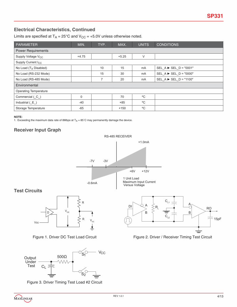
Figure 1. Driver DC Test Load Circuit
Electrical Characteristics, ContinuedLimits are specified at TA = 25°C and VCC = +5.0V unless otherwise noted.
PARAMETER MIN. TYP. MAX. UNITS CONDITIONS
Power Requirements
Supply Voltage VCC +4.75 +5.25 V
Supply Current ICC
No Load (TX Disabled) 10 15 mA SEL_A SEL_D = "0001"
No Load (RS-232 Mode) 15 30 mA SEL_A SEL_D = "0000"
No Load (RS-485 Mode) 7 20 mA SEL_A SEL_D = "1100"
Environmental
Operating Temperature
Commercial (_C_) 0 70 ºC
Industrial (_E_) -40 +85 ºC
Storage Temperature -65 +150 ºC
NOTE:1. Exceeding the maximum data rate of 8Mbps at TA = 85˚C may permanently damage the device.
Receiver Input Graph
Figure 3. Driver Timing Test Load #2 Circuit
Figure 2. Driver / Receiver Timing Test Circuit
R
R VOC
D
Vcc
VOD
CL1
15pF
ROA
B
A
B
DI
CL2
RL
500Ω
CL
OutputUnderTest
S1
S2
VCC
RS-485 RECEIVER
+1.0mA
-0.6mA
+6V +12V
-3V-7V
Maximum Input CurrentVersus Voltage
1 Unit Load
SP331
5/13REV 1.0.1
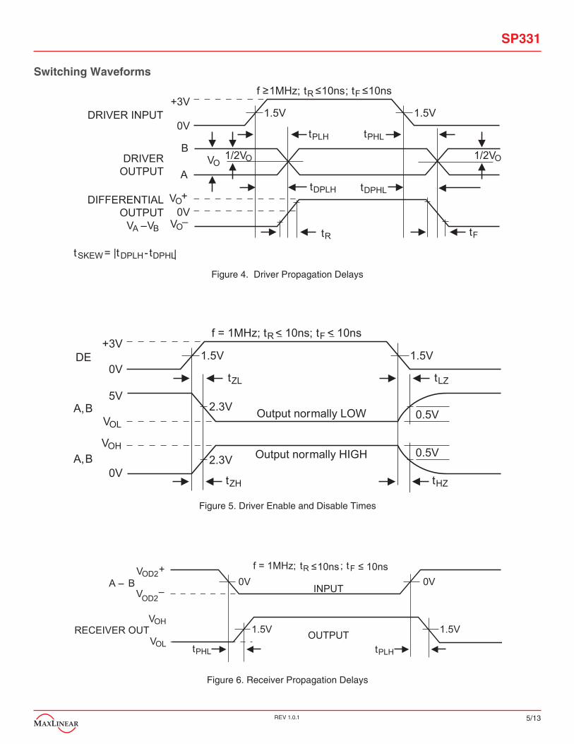
Switching Waveforms
Figure 4. Driver Propagation Delays
Figure 5. Driver Enable and Disable Times
Figure 6. Receiver Propagation Delays
+3V
0VDRIVER INPUT
A
BDRIVER
OUTPUT
VO+DIFFERENTIALOUTPUT
VA – VB
0VVO–
1.5V 1.5V
tPLH
tFtR
f ≥ 1MHz; tR ≤ 10ns; tF ≤ 10ns
VO1/2VO 1/2VO
tPHL
tSKEW = |tDPLH - tDPHL|
tDPLH tDPHL
+3V
0VDE
5V
VOL
A, B0V
1.5V 1.5V
tZL
tZH
f = 1MHz; tR < 10ns; tF < 10ns
VOH
A, B 2.3V
2.3V
tLZ
tHZ
0.5V
0.5V
Output normally LOW
Output normally HIGH
VOH
VOLRECEIVER OUT 1.5V 1.5V
tPHL
f = 1MHz; tR 10ns; tF ≤ 10ns
OUTPUT
VOD2+
VOD2–
A – B 0V 0V
tPLH
INPUT
≤
SP331
6/13REV 1.0.1
Switching Waveforms (Continued)
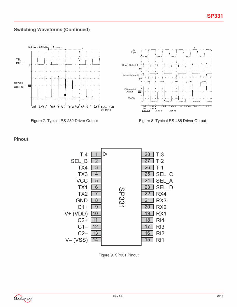
Figure 7. Typical RS-232 Driver Output Figure 8. Typical RS-485 Driver Output
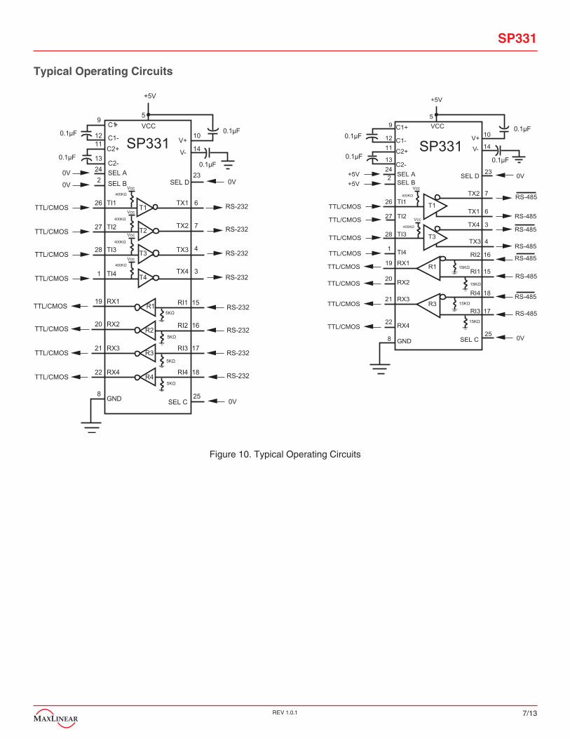
Figure 9. SP331 Pinout
TTLINPUT
DRIVEROUTPUT
TTLInput
Driver Output A
Driver Output B
DifferentialOutput
VA - VB
Pinout
TI4SEL_B
TX4TX3VCCTX1TX2
GNDC1+
V+ (VDD)C2+C1–C2–
V– (VSS)
TI3TI2TI1SEL_CSEL_ASEL_DRX4RX3RX2RX1RI4RI3RI2RI1
2827262524232221201918171615
123456789
1011121314
SP
331
SP331
7/13REV 1.0.1
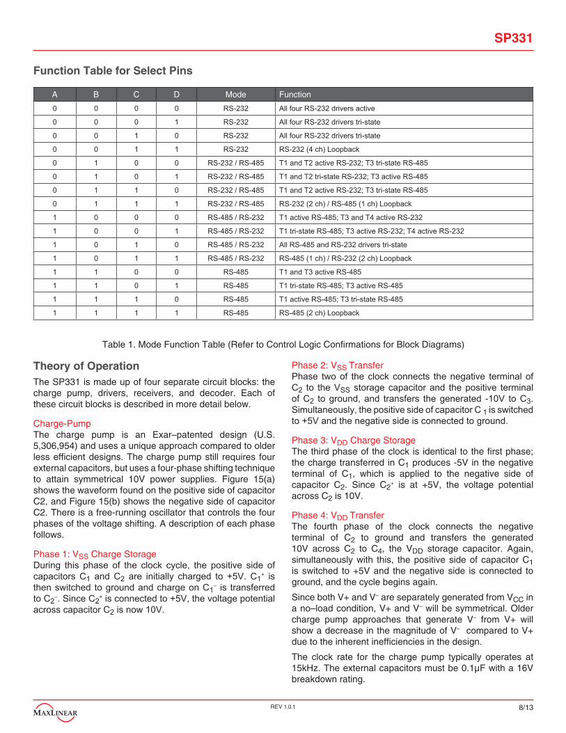
Typical Operating Circuits
SEL A
TTL/CMOS
TTL/CMOS
TTL/CMOS
C1+
C1-
C2+
C2-
1
SEL B 2
+5V
VCC5
GND8
9
1112
13
19
20
22
24
26
27
28
TTL/CMOS
TTL/CMOS
TTL/CMOS
TTL/CMOS
T1
T3
R1
RS-485
RS-485
RS-485
0V
V+
V-
0VSEL C
RS-485
RS-485
RS-485
4
6
7
10
14
15
16
23
25
3
RI1
RI2
TX3
TX4
TX1
TX2TI1
TI2
TI3
TI4
RX1
RX2
TTL/CMOS21
R317
18RI4
RI3
RX3
RX415KΩ
400KΩ
Vcc
400KΩ
Vcc
SEL D
RS-485
RS-485
+5V+5V
+5V
GND
TTL/CMOS
TTL/CMOS
TTL/CMOS
TTL/CMOS
0V
0.1µFVCC
V+
V-
0VSEL C
RS-232
TTL/CMOS
TTL/CMOS
TTL/CMOS
TTL/CMOS
T1
T2
T3
T4
TX1
TX2
TX3
TX4
TI1
TI2
TI3
TI4
RI1
RI2
RI3
RI4
RX1
RX2
RX3
RX4
1 3
4
5
6
7
8
10C1+
C1-C2+
C2-
9
1112
1314
15
16
17
18
19
20
21
22
23SEL B 2SEL A 24
25
26
27
28
R1
R2
R3
R4
5KΩ
400KΩVcc
Vcc
Vcc
Vcc
RS-232
RS-232
RS-232
RS-232
RS-232
RS-232
RS-232
SEL D 0V
0V
SP331 SP3310.1µF
0.1µF
0.1µF
400KΩ
400KΩ
400KΩ
5KΩ
5KΩ
5KΩ
0.1µF
0.1µF 0.1µF
0.1µF
15KΩ
15KΩ
15KΩ
Figure 10. Typical Operating Circuits
SP331
8/13REV 1.0.1
Function Table for Select Pins
A B C D Mode Function
0 0 0 0 RS-232 All four RS-232 drivers active
0 0 0 1 RS-232 All four RS-232 drivers tri-state
0 0 1 0 RS-232 All four RS-232 drivers tri-state
0 0 1 1 RS-232 RS-232 (4 ch) Loopback
0 1 0 0 RS-232 / RS-485 T1 and T2 active RS-232; T3 tri-state RS-485
0 1 0 1 RS-232 / RS-485 T1 and T2 tri-state RS-232; T3 active RS-485
0 1 1 0 RS-232 / RS-485 T1 and T2 active RS-232; T3 tri-state RS-485
0 1 1 1 RS-232 / RS-485 RS-232 (2 ch) / RS-485 (1 ch) Loopback
1 0 0 0 RS-485 / RS-232 T1 active RS-485; T3 and T4 active RS-232
1 0 0 1 RS-485 / RS-232 T1 tri-state RS-485; T3 active RS-232; T4 active RS-232
1 0 1 0 RS-485 / RS-232 All RS-485 and RS-232 drivers tri-state
1 0 1 1 RS-485 / RS-232 RS-485 (1 ch) / RS-232 (2 ch) Loopback
1 1 0 0 RS-485 T1 and T3 active RS-485
1 1 0 1 RS-485 T1 tri-state RS-485; T3 active RS-485
1 1 1 0 RS-485 T1 active RS-485; T3 tri-state RS-485
1 1 1 1 RS-485 RS-485 (2 ch) Loopback
Table 1. Mode Function Table (Refer to Control Logic Confirmations for Block Diagrams)
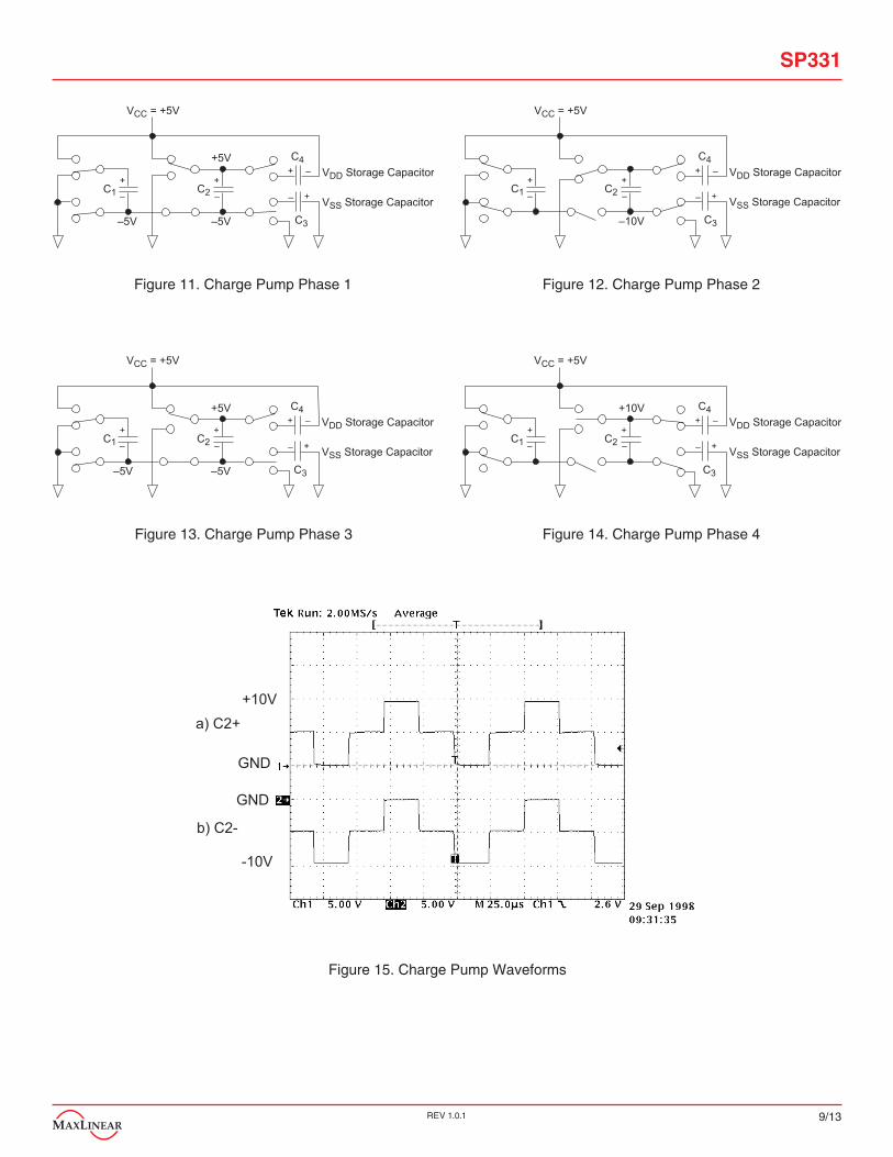
Theory of OperationThe SP331 is made up of four separate circuit blocks: the charge pump, drivers, receivers, and decoder. Each of these circuit blocks is described in more detail below.
Charge-PumpThe charge pump is an Exar–patented design (U.S. 5,306,954) and uses a unique approach compared to older less efficient designs. The charge pump still requires four external capacitors, but uses a four-phase shifting technique to attain symmetrical 10V power supplies. Figure 15(a) shows the waveform found on the positive side of capacitor C2, and Figure 15(b) shows the negative side of capacitor C2. There is a free-running oscillator that controls the four phases of the voltage shifting. A description of each phase follows.
Phase 1: VSS Charge StorageDuring this phase of the clock cycle, the positive side of capacitors C1 and C2 are initially charged to +5V. C1+ is then switched to ground and charge on C1– is transferred to C2–. Since C2+ is connected to +5V, the voltage potential across capacitor C2 is now 10V.
Phase 2: VSS TransferPhase two of the clock connects the negative terminal of C2 to the VSS storage capacitor and the positive terminal of C2 to ground, and transfers the generated -10V to C3. Simultaneously, the positive side of capacitor C 1 is switched to +5V and the negative side is connected to ground.
Phase 3: VDD Charge StorageThe third phase of the clock is identical to the first phase; the charge transferred in C1 produces -5V in the negative terminal of C1, which is applied to the negative side of capacitor C2. Since C2
+ is at +5V, the voltage potential across C2 is 10V.
Phase 4: VDD TransferThe fourth phase of the clock connects the negative terminal of C2 to ground and transfers the generated 10V across C2 to C4, the VDD storage capacitor. Again, simultaneously with this, the positive side of capacitor C1 is switched to +5V and the negative side is connected to ground, and the cycle begins again.
Since both V+ and V– are separately generated from VCC in a no–load condition, V+ and V– will be symmetrical. Older charge pump approaches that generate V– from V+ will show a decrease in the magnitude of V– compared to V+ due to the inherent inefficiencies in the design.
The clock rate for the charge pump typically operates at 15kHz. The external capacitors must be 0.1µF with a 16V breakdown rating.
SP331
9/13REV 1.0.1
Figure 11. Charge Pump Phase 1 Figure 12. Charge Pump Phase 2
Figure 13. Charge Pump Phase 3 Figure 14. Charge Pump Phase 4
Figure 15. Charge Pump Waveforms
VCC = +5V
–5V –5V
+5V
VSS Storage Capacitor
VDD Storage CapacitorC1 C2
C3
C4+
+
+ +–
–––
VCC = +5V
–10V
VSS Storage Capacitor
VDD Storage CapacitorC1 C2
C3
C4+
+
+ +–
–––
VCC = +5V
–5V
+5V
–5V
VSS Storage Capacitor
VDD Storage CapacitorC1 C2
C3
C4+
+
+ +–
–––
VCC = +5V
+10V
VSS Storage Capacitor
VDD Storage CapacitorC1 C2
C3
C4+
+
+ +–
–––
+10V
GND
GND
-10V
a) C2+
b) C2-
SP331
10/13REV 1.0.1
External Power SuppliesFor applications that do not require +5V only, external supplies can be applied at the V+ and V– pins. The value of the external supply voltages must be no greater than ±10V. The current drain for the ±10V supplies is used for RS-232. For the RS-232 driver the current requirement will be 3.5mA per driver. The external power supplies should provide a power supply sequence of: +10V, then +5V, followed by -10V.
Drivers
The SP331 has four independent RS-232 single-ended drivers and two differential RS-485 drivers. Control for the mode selection is done via a four–bit control word. The drivers are pre-arranged such that for each mode of operation the relative position and functionality of the drivers are set up to accommodate the selected interface mode. As the mode of the drivers is changed, the electrical characteristics will change to support the requirements of clock, data, and control line signal levels. Unused driver inputs can be left floating; however, to ensure a desired state with no input signal, pull–up resistors to +5V or pull–down resistors to ground are suggested. Since the driver inputs are both TTL or CMOS compatible, any value resistor less than 100kΩ will suffice.When in RS-232 mode, the single-ended RS-232 drivers produce compliant RS-232E and ITU V.28 signals. Each of the four drivers output single-ended bipolar signals in excess of ±5V with a full load of 3kΩ and 2500pF applied as specified. These drivers can also operate at least 120kbps.
When programmed to RS-485 mode, the differential RS-485 drivers produce complaint RS-485 signals. Each RS-485 driver outputs a unipolar signal on each output pin with a magnitude of at least 1.5V while loaded with a worst case of 54Ω between the driver’s two output pins. The signal levels and drive capability of the RS-485 drivers allow the drivers to also comply with RS-422 levels. The transmission rate for the differential drivers is 10Mbps.
ReceiversThe SP331 has four single-ended receivers when programmed for RS-232 mode and two differential receivers when programmed for RS-485 mode.
Control for the mode selection is done via a 4–bit control word, as in the drivers. As the operating mode of the receivers is changed, the electrical characteristics will change to support the requirements of the appropriate serial standard. Unused receiver inputs can be left floating without causing oscillation. To ensure a desired state of the receiver output, a pull–up resistor of 100kΩ to +5V should be connected to the inverting input for a logic low, or the non–inverting input for a logic high. For single-ended receivers, a pull–down resistor to ground of 5kΩ is internally connected, which will ensure a logic high output.
The RS-232 receiver has a single–ended input with a threshold of 0.8V to 2.4V. The RS-232 receiver has an operating voltage range of ±15V and can receive signals up to 120kbps. RS-232 receivers are used in RS-232 mode for all signal types include data, clock, and control lines of the RS-232 serial port.
The differential RS-485 receiver has an input impedance of 15kΩ and a differential threshold of ±200mV. Since the characteristics of an RS-422 receiver are actually subsets of RS-485, the receivers for RS-422 requirements are identical to the RS-485 receivers. All of the differential receivers can receive data up to 10Mbps.
Select Mode PinsSimilar to our SP500 family of multiprotocol products, the SP331 has the ability to change the configuration of the drivers and receivers via a 4–bit switch. Referring to Table 1; RS-232 mode, RS-485 mode, or two different combinations of RS-232/RS-485 can be configured using the SEL_A and SEL_B pins. The drivers can be put into tri-state mode by using the SEL_C and SEL_D pins. All receivers remain active during any tri-state condition of the drivers.
Loopback ModeLoopback is invoked by asserting “xx11” into the select pins. In RS-232 / RS-485 or RS-485 / RS-232 loopback mode, the RS-232 driver outputs loop back into the RS-232 receiver inputs and the RS-485 differential driver loops back into the RS-485 receiver. During loopback, the driver outputs and receiver inputs are disconnected from the outside world. The driver outputs are in tri-state and the receiver inputs are disabled. The input impedance of the receivers during loopback is approximately 15kΩ to ground.
SP331
11/13REV 1.0.1
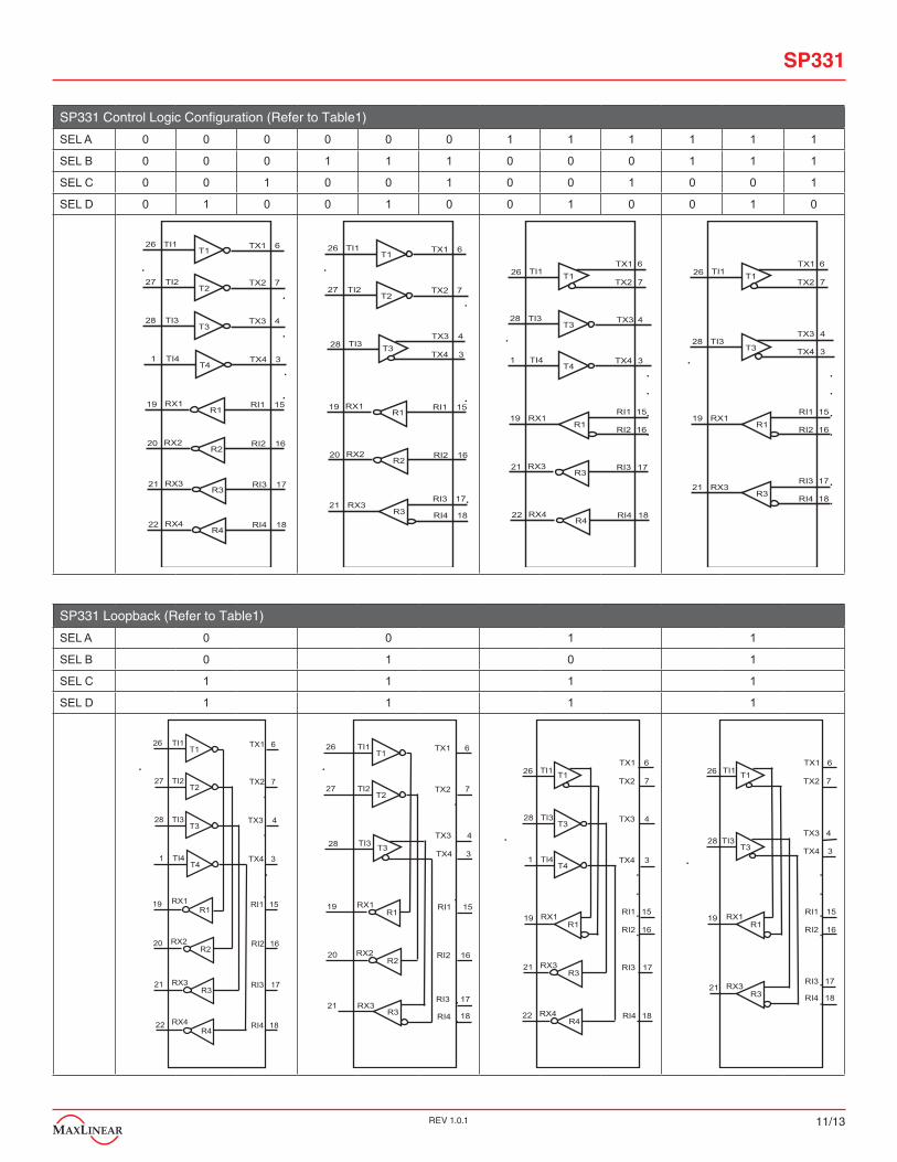
SP331 Control Logic Configuration (Refer to Table1)
SEL A 0 0 0 0 0 0 1 1 1 1 1 1
SEL B 0 0 0 1 1 1 0 0 0 1 1 1
SEL C 0 0 1 0 0 1 0 0 1 0 0 1
SEL D 0 1 0 0 1 0 0 1 0 0 1 0
26T1
7
6
TX2
TX1TI1
R1RX119 15RI1
T2TI227
R2RX220 16RI2
4TX3T3
TI328
3TX4T4
TI41
R3RX321 17RI3
R4RX422 18RI4
26T1
7
4
3
6
TX2
TX1
TX3
TX4
TI1
21R3 18
17RI3
RI4RX3
T3
R1RX119
28 TI3
15RI1
T2TI227
R2RX220 16RI2
28T3
3
6
7
4
TX4
TX3
TX1
TX2
TI3
19R1
16
15RI1
RI2RX1
T1
R3RX321
26 TI1
17RI3
T4TI41
R4RX422 18RI4
28T3 3
6
7
4
TX4
TX3
TX1
TX2
TI3
19R1
16
15RI1
RI2RX1
T126 TI1
21R3
18
17RI3
RI4RX3
SP331 Loopback (Refer to Table1)
SEL A 0 0 1 1
SEL B 0 1 0 1
SEL C 1 1 1 1
SEL D 1 1 1 1
26T1
7
6
TX2
TX1TI1
R1RX119 15RI1
T2TI227
R2RX220 16RI2
4TX3T3
TI328
3TX4T4
TI41
R3RX321 17RI3
R4RX422 18RI4
26T1
7
4
3
6
TX2
TX1
TX3
TX4
TI1
21R3 18
17RI3
RI4RX3
T3
R1RX119
28 TI3
15RI1
T2TI227
R2RX220 16RI2
28T3
3
6
7
4
TX4
TX3
TX1
TX2
TI3
19R1
16
15RI1
RI2
RX1
T1
R3RX321
26 TI1
17RI3
T4TI41
R4RX422 18RI4
28T3 3
6
7
4
TX4
TX3
TX1
TX2
TI3
19R1
16
15RI1
RI2
RX1
T126 TI1
21R3 18
17RI3
RI4RX3
SP331
12/13REV 1.0.1
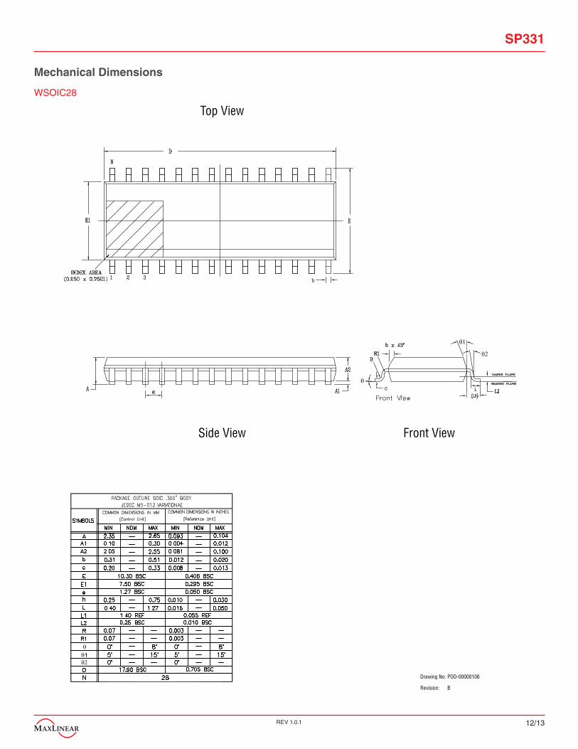
Mechanical Dimensions
WSOIC28
Drawing No: POD-00000106
Revision: B
Side View
Top View
Front View
SP331
The content of this document is furnished for informational use only, is subject to change without notice, and should not be construed as a commitment by MaxLinear, Inc.. MaxLinear, Inc. assumes no responsibility or liability for any errors or inaccuracies that may appear in the informational content contained in this guide. Complying with all applicable copyright laws is the responsibility of the user. Without limiting the rights under copyright, no part of this document may be reproduced into, stored in, or introduced into a retrieval system, or transmitted in any form or by any means (electronic, mechanical, photocopying, recording, or otherwise), or for any purpose, without the express written permission of MaxLinear, Inc.
Maxlinear, Inc. does not recommend the use of any of its products in life support applications where the failure or malfunction of the product can reasonably be expected to cause failure of the life support system or to significantly affect its safety or effectiveness. Products are not authorized for use in such applications unless MaxLinear, Inc. receives, in writing, assurances to its satisfaction that: (a) the risk of injury or damage has been minimized; (b) the user assumes all such risks; (c) potential liability of MaxLinear, Inc. is adequately protected under the circumstances.
MaxLinear, Inc. may have patents, patent applications, trademarks, copyrights, or other intellectual property rights covering subject matter in this document. Except as expressly provided in any written license agreement from MaxLinear, Inc., the furnishing of this document does not give you any license to these patents, trademarks, copyrights, or other intellectual property.
Company and product names may be registered trademarks or trademarks of the respective owners with which they are associated.
© 2010 - 2018 MaxLinear, Inc. All rights reserved
SP331_DS_031918 13/13REV 1.0.1
Corporate Headquarters: 5966 La Place Court Suite 100 Carlsbad, CA 92008 Tel.:+1 (760) 692-0711 Fax: +1 (760) 444-8598 www.maxlinear.com
High Performance Analog: 1060 Rincon CircleSan Jose, CA 95131Tel.: +1 (669) 265-6100Fax: +1 (669) 265-6101Email: [email protected]
Ordering Information(1)
Part Number Operating Temperature Range Lead-Free Package Packaging Method
SP331CT-L0°C to 70°C
Yes(2) 28-pin WSOIC
Tube
SP331CT-L/TR Reel
SP331ET-L-40°C to 85°C
Tube
SP331ET-L/TR Reel
NOTE:1. Refer to www.exar.com/SP331 for most up-to-date Ordering Information.2. Visit www.exar.com for additional information on Environmental Rating.
Revision History
Revision Date Description
01/04/05 -- Legacy Sipex Datasheet
01/26/10 1.0.0 Convert to Exar Format. Add Revision History table. Change revision to 1.0.0. Add Note 1 and change maximum RS-485 data rate at +85C. Update ABS Max Rating table.
03/19/18 1.0.1 Update to MaxLinear logo. Update format and ordering information table. RS-485 Driver En-able Timing moved on page 3.