SN74LVC1G07-EP SINGLE BUFFER/DRIVER WITH OPEN …
12
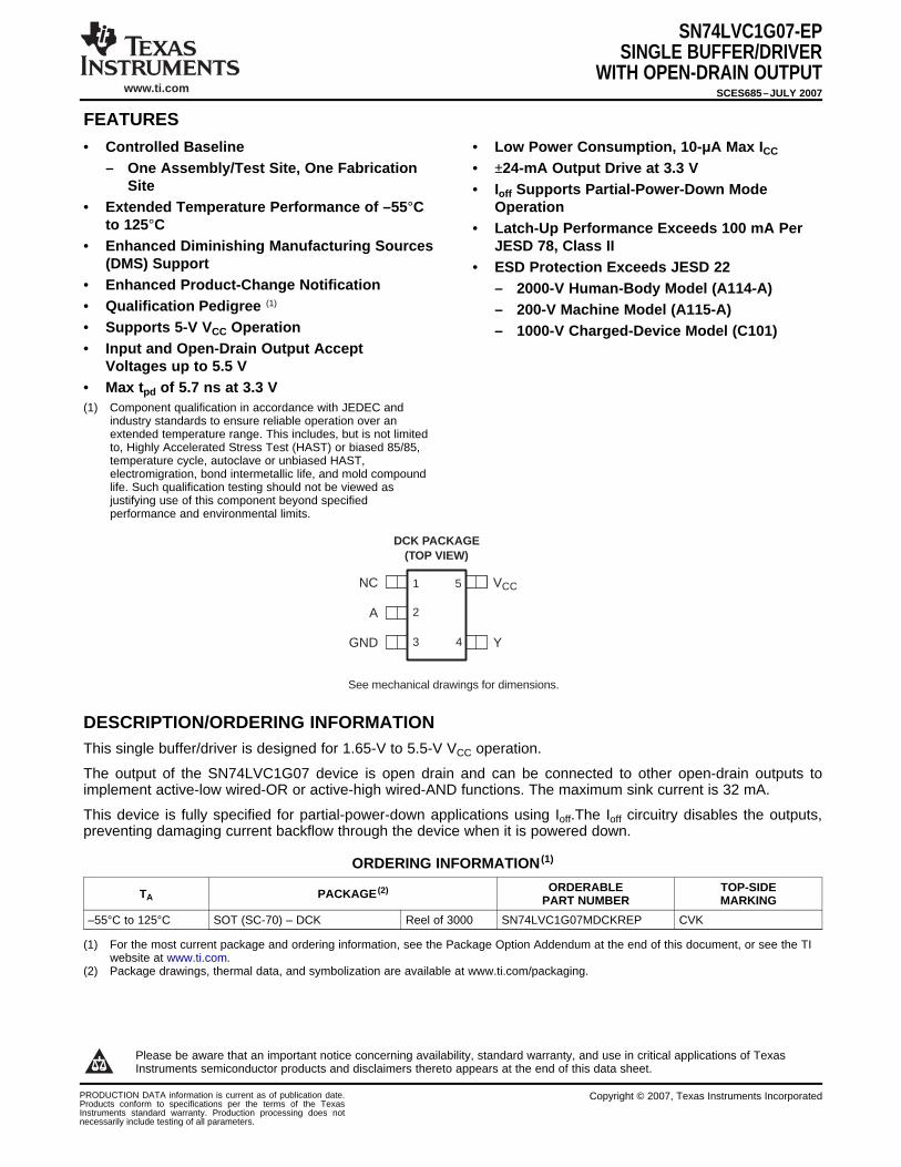
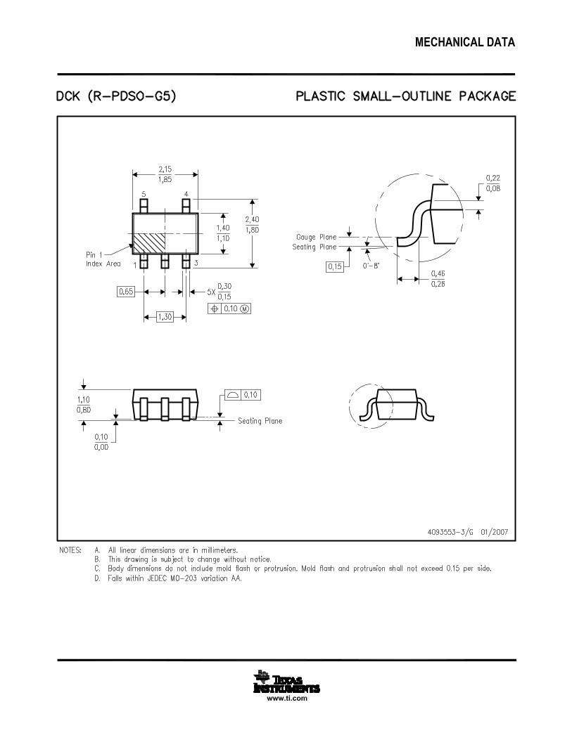
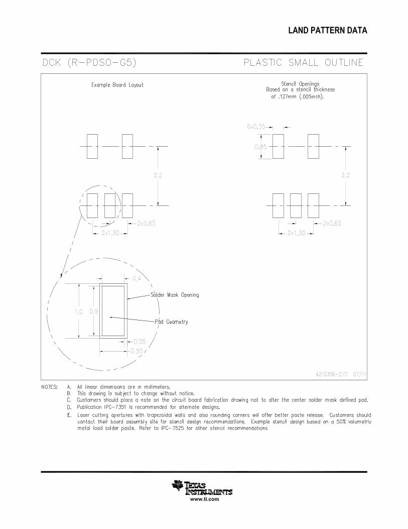
www.ti.com FEATURES 3 2 4 5 1 NC V CC Y A GND DCK PACKAGE (TOP VIEW) See mechanical drawings for dimensions. DESCRIPTION/ORDERING INFORMATION SN74LVC1G07-EP SINGLE BUFFER/DRIVER WITH OPEN-DRAIN OUTPUT SCES685 – JULY 2007 • Controlled Baseline • Low Power Consumption, 10-μA Max I CC – One Assembly/Test Site, One Fabrication • ±24-mA Output Drive at 3.3 V Site • I off Supports Partial-Power-Down Mode • Extended Temperature Performance of –55°C Operation to 125°C • Latch-Up Performance Exceeds 100 mA Per • Enhanced Diminishing Manufacturing Sources JESD 78, Class II (DMS) Support • ESD Protection Exceeds JESD 22 • Enhanced Product-Change Notification – 2000-V Human-Body Model (A114-A) • Qualification Pedigree (1) – 200-V Machine Model (A115-A) • Supports 5-V V CC Operation – 1000-V Charged-Device Model (C101) • Input and Open-Drain Output Accept Voltages up to 5.5 V • Max t pd of 5.7 ns at 3.3 V (1) Component qualification in accordance with JEDEC and industry standards to ensure reliable operation over an extended temperature range. This includes, but is not limited to, Highly Accelerated Stress Test (HAST) or biased 85/85, temperature cycle, autoclave or unbiased HAST, electromigration, bond intermetallic life, and mold compound life. Such qualification testing should not be viewed as justifying use of this component beyond specified performance and environmental limits. This single buffer/driver is designed for 1.65-V to 5.5-V V CC operation. The output of the SN74LVC1G07 device is open drain and can be connected to other open-drain outputs to implement active-low wired-OR or active-high wired-AND functions. The maximum sink current is 32 mA. This device is fully specified for partial-power-down applications using I off .The I off circuitry disables the outputs, preventing damaging current backflow through the device when it is powered down. ORDERING INFORMATION (1) ORDERABLE TOP-SIDE T A PACKAGE (2) PART NUMBER MARKING –55°C to 125°C SOT (SC-70) – DCK Reel of 3000 SN74LVC1G07MDCKREP CVK (1) For the most current package and ordering information, see the Package Option Addendum at the end of this document, or see the TI website at www.ti.com. (2) Package drawings, thermal data, and symbolization are available at www.ti.com/packaging. Please be aware that an important notice concerning availability, standard warranty, and use in critical applications of Texas Instruments semiconductor products and disclaimers thereto appears at the end of this data sheet. PRODUCTION DATA information is current as of publication date. Copyright © 2007, Texas Instruments Incorporated Products conform to specifications per the terms of the Texas Instruments standard warranty. Production processing does not necessarily include testing of all parameters.
Transcript of SN74LVC1G07-EP SINGLE BUFFER/DRIVER WITH OPEN …
www.ti.com
FEATURES
3
2
4
51NC VCC
Y
A
GND
DCK PACKAGE(TOP VIEW)
See mechanical drawings for dimensions.
DESCRIPTION/ORDERING INFORMATION
SN74LVC1G07-EPSINGLE BUFFER/DRIVER
WITH OPEN-DRAIN OUTPUTSCES685–JULY 2007
• Controlled Baseline • Low Power Consumption, 10-μA Max ICC
– One Assembly/Test Site, One Fabrication • ±24-mA Output Drive at 3.3 VSite • Ioff Supports Partial-Power-Down Mode
• Extended Temperature Performance of –55°C Operationto 125°C • Latch-Up Performance Exceeds 100 mA Per
• Enhanced Diminishing Manufacturing Sources JESD 78, Class II(DMS) Support • ESD Protection Exceeds JESD 22
• Enhanced Product-Change Notification – 2000-V Human-Body Model (A114-A)• Qualification Pedigree (1) – 200-V Machine Model (A115-A)• Supports 5-V VCC Operation – 1000-V Charged-Device Model (C101)• Input and Open-Drain Output Accept
Voltages up to 5.5 V• Max tpd of 5.7 ns at 3.3 V(1) Component qualification in accordance with JEDEC and
industry standards to ensure reliable operation over anextended temperature range. This includes, but is not limitedto, Highly Accelerated Stress Test (HAST) or biased 85/85,temperature cycle, autoclave or unbiased HAST,electromigration, bond intermetallic life, and mold compoundlife. Such qualification testing should not be viewed asjustifying use of this component beyond specifiedperformance and environmental limits.
This single buffer/driver is designed for 1.65-V to 5.5-V VCC operation.
The output of the SN74LVC1G07 device is open drain and can be connected to other open-drain outputs toimplement active-low wired-OR or active-high wired-AND functions. The maximum sink current is 32 mA.
This device is fully specified for partial-power-down applications using Ioff.The Ioff circuitry disables the outputs,preventing damaging current backflow through the device when it is powered down.
ORDERING INFORMATION (1)
ORDERABLE TOP-SIDETA PACKAGE (2)PART NUMBER MARKING
–55°C to 125°C SOT (SC-70) – DCK Reel of 3000 SN74LVC1G07MDCKREP CVK
(1) For the most current package and ordering information, see the Package Option Addendum at the end of this document, or see the TIwebsite at www.ti.com.
(2) Package drawings, thermal data, and symbolization are available at www.ti.com/packaging.
Please be aware that an important notice concerning availability, standard warranty, and use in critical applications of TexasInstruments semiconductor products and disclaimers thereto appears at the end of this data sheet.
PRODUCTION DATA information is current as of publication date. Copyright © 2007, Texas Instruments IncorporatedProducts conform to specifications per the terms of the TexasInstruments standard warranty. Production processing does notnecessarily include testing of all parameters.
www.ti.com
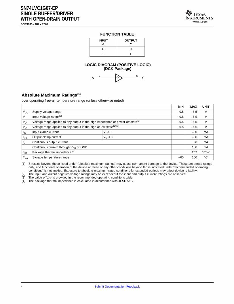
A Y2 4
Absolute Maximum Ratings (1)
SN74LVC1G07-EPSINGLE BUFFER/DRIVERWITH OPEN-DRAIN OUTPUTSCES685–JULY 2007
FUNCTION TABLE
INPUT OUTPUTA Y
H H
L L
LOGIC DIAGRAM (POSITIVE LOGIC)(DCK Package)
over operating free-air temperature range (unless otherwise noted)
MIN MAX UNIT
VCC Supply voltage range –0.5 6.5 V
VI Input voltage range (2) –0.5 6.5 V
VO Voltage range applied to any output in the high-impedance or power-off state (2) –0.5 6.5 V
VO Voltage range applied to any output in the high or low state (2) (3) –0.5 6.5 V
IIK Input clamp current VI < 0 –50 mA
IOK Output clamp current VO < 0 –50 mA
IO Continuous output current 50 mA
Continuous current through VCC or GND 100 mA
θJA Package thermal impedance (4) 252 °C/W
Tstg Storage temperature range –65 150 °C
(1) Stresses beyond those listed under "absolute maximum ratings" may cause permanent damage to the device. These are stress ratingsonly, and functional operation of the device at these or any other conditions beyond those indicated under "recommended operatingconditions" is not implied. Exposure to absolute-maximum-rated conditions for extended periods may affect device reliability.
(2) The input and output negative-voltage ratings may be exceeded if the input and output current ratings are observed.(3) The value of VCC is provided in the recommended operating conditions table.(4) The package thermal impedance is calculated in accordance with JESD 51-7.
2 Submit Documentation Feedback
www.ti.com
Recommended Operating Conditions (1)
Electrical Characteristics
SN74LVC1G07-EPSINGLE BUFFER/DRIVER
WITH OPEN-DRAIN OUTPUTSCES685–JULY 2007
MIN MAX UNIT
Operating 1.65 5.5VCC Supply voltage V
Data retention only 1.5
VCC = 1.65 V to 1.95 V 0.65 × VCC
VCC = 2.3 V to 2.7 V 1.7VIH High-level input voltage V
VCC = 3 V to 3.6 V 2
VCC = 4.5 V to 5.5 V 0.7 × VCC
VCC = 1.65 V to 1.95 V 0.35 × VCC
VCC = 2.3 V to 2.7 V 0.7VIL Low-level input voltage V
VCC = 3 V to 3.6 V 0.8
VCC = 4.5 V to 5.5 V 0.3 × VCC
VI Input voltage 0 5.5 V
VO Output voltage 0 5.5 V
VCC = 1.65 V 4
VCC = 2.3 V 8
IOL Low-level output current 16 mAVCC = 3 V
24
VCC = 4.5 V 32
VCC = 1.8 V ±0.15 V, 2.5 V ± 0.2 V 20
Δt/Δv Input transition rise or fall rate VCC = 3.3 V ± 0.3 V 10 ns/V
VCC = 5 V ± 0.5 V 5
TA Operating free-air temperature –55 125 °C
(1) All unused inputs of the device must be held at VCC or GND to ensure proper device operation. Refer to the TI application report,Implications of Slow or Floating CMOS Inputs, literature number SCBA004.
over recommended operating free-air temperature range (unless otherwise noted)
PARAMETER TEST CONDITIONS VCC MIN TYP (1) MAX UNIT
IOL = 100 μA 1.65 V to 5.5 V 0.1
IOL = 4 mA 1.65 V 0.45
IOL = 8 mA 2.3 V 0.3VOL V
IOL = 16 mA 0.43 V
IOL = 24 mA 0.55
IOL = 32 mA 4.5 V 0.55
II A input VI = 5.5 V or GND 0 to 5.5 V ±5 μA
Ioff VI or VO = 5.5 V 0 ±10 μA
ICC VI = 5.5 V or GND, IO = 0 1.65 V to 5.5 V 10 μA
ΔICC One input at VCC – 0.6 V, Other inputs at VCC or GND 3 V to 5.5 V 500 μA
Ci VI = VCC or GND 3.3 V 4 pF
Co VO = VCC or GND 3.3 V 5 pF
(1) All typical values are at VCC = 3.3 V, TA = 25°C.
3Submit Documentation Feedback
www.ti.com
Switching Characteristics
Operating Characteristics
SN74LVC1G07-EPSINGLE BUFFER/DRIVERWITH OPEN-DRAIN OUTPUTSCES685–JULY 2007
over recommended operating free-air temperature range (unless otherwise noted) (see Figure 1)
VCC = 3.3 V VCC = 5 VFROM TO ± 0.3 V ± 0.5 VPARAMETER UNIT(INPUT) (OUTPUT)
MIN MAX MIN MAX
tpd A Y 1.5 5.7 1 4.9 ns
TA = 25°C
VCC = 3.3 V VCC = 5 VPARAMETER TEST CONDITIONS f = 10 MHz UNIT
TYP TYP
Cpd Power dissipation capacitance 4 6 pF
4 Submit Documentation Feedback
www.ti.com
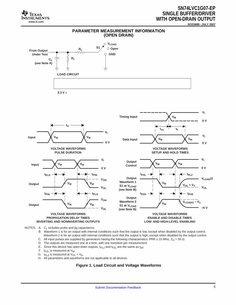
PARAMETER MEASUREMENT INFORMATION
VM
thtsu
From OutputUnder Test
CL(see Note A)
LOAD CIRCUIT
S1VLOAD
Open
GNDRL
RL
Data Input
Timing InputVI
0 V
VI
0 V0 V
tw
Input
VOLTAGE WAVEFORMSSETUP AND HOLD TIMES
VOLTAGE WAVEFORMSPROPAGATION DELAY TIMES
INVERTING AND NONINVERTING OUTPUTS
VOLTAGE WAVEFORMSPULSE DURATION
tPLH
tPHL
tPHL
tPLH
VOH
VOH
VOL
VOL
VI
0 VInput
OutputWaveform 1S1 at VLOAD(see Note B)
OutputWaveform 2S1 at VLOAD(see Note B)
VOL
tPZL
tPZH
tPLZ
tPHZ
VLOAD/2
0 V
VOL + V∆
VLOAD/2 − V∆
≈0 V
VI
VOLTAGE WAVEFORMSENABLE AND DISABLE TIMES
LOW- AND HIGH-LEVEL ENABLING
Output
Output
NOTES: A. CL includes probe and jig capacitance.B. Waveform 1 is for an output with internal conditions such that the output is low, except when disabled by the output control.
Waveform 2 is for an output with internal conditions such that the output is high, except when disabled by the output control.C. All input pulses are supplied by generators having the following characteristics: PRR ≤ 10 MHz, ZO = 50 Ω.D. The outputs are measured one at a time, with one transition per measurement.E. Since this device has open-drain outputs, tPLZ and tPZL are the same as tpd.F. tPZL is measured at VM.G. tPLZ is measured at VOL + V∆.H. All parameters and waveforms are not applicable to all devices.
OutputControl
VM VM
VM VM
VM VM
VM
VM VM
VM
VM
VM
VI
VM
VM
3.3 V ± 0.3 V5 V ± 0.5 V
500 Ω500 Ω
VCC RL
6 V2 × VCC
VLOAD CL
50 pF50 pF
0.3 V0.3 V
V∆
3 VVCC
VI
1.5 VVCC/2
VMtr/tf
≤ 2.5 ns≤ 2.5 ns
INPUT
tPZL (see Notes E and F)
tPLZ (see Notes E and G)
tPHZ/tPZH
VLOAD
VLOAD
VLOAD
TEST S1
VLOAD/2
SN74LVC1G07-EPSINGLE BUFFER/DRIVER
WITH OPEN-DRAIN OUTPUTSCES685–JULY 2007
(OPEN DRAIN)
Figure 1. Load Circuit and Voltage Waveforms
5Submit Documentation Feedback
PACKAGE OPTION ADDENDUM
www.ti.com 11-Apr-2013
Addendum-Page 1
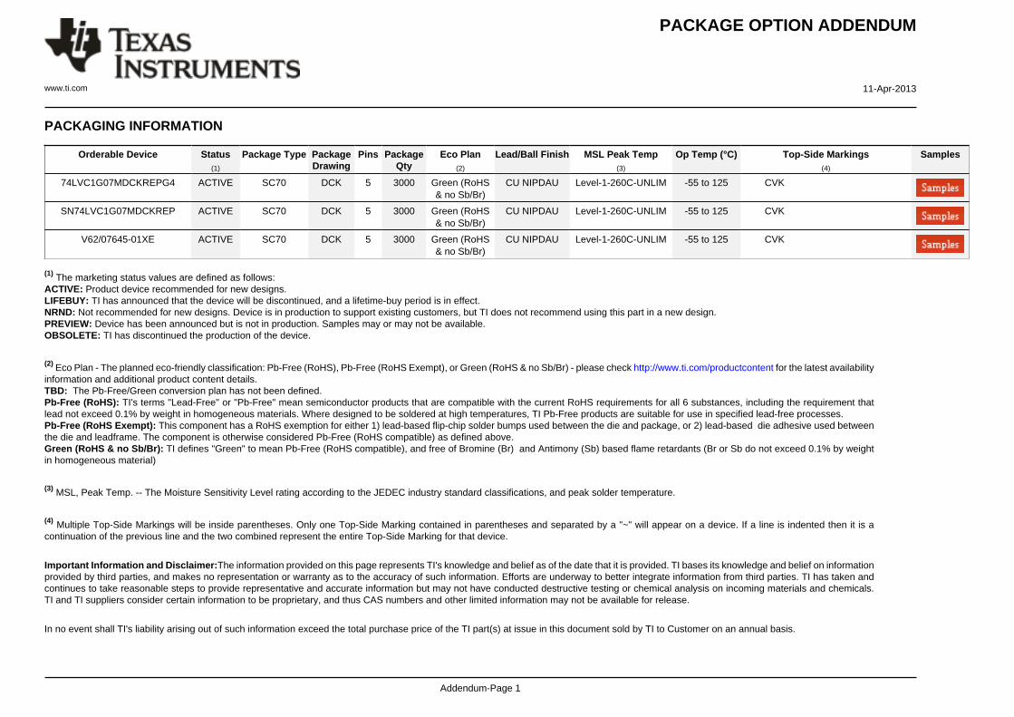
PACKAGING INFORMATION
Orderable Device Status(1)
Package Type PackageDrawing
Pins PackageQty
Eco Plan(2)
Lead/Ball Finish MSL Peak Temp(3)
Op Temp (°C) Top-Side Markings(4)
Samples
74LVC1G07MDCKREPG4 ACTIVE SC70 DCK 5 3000 Green (RoHS& no Sb/Br)
CU NIPDAU Level-1-260C-UNLIM -55 to 125 CVK
SN74LVC1G07MDCKREP ACTIVE SC70 DCK 5 3000 Green (RoHS& no Sb/Br)
CU NIPDAU Level-1-260C-UNLIM -55 to 125 CVK
V62/07645-01XE ACTIVE SC70 DCK 5 3000 Green (RoHS& no Sb/Br)
CU NIPDAU Level-1-260C-UNLIM -55 to 125 CVK
(1) The marketing status values are defined as follows:ACTIVE: Product device recommended for new designs.LIFEBUY: TI has announced that the device will be discontinued, and a lifetime-buy period is in effect.NRND: Not recommended for new designs. Device is in production to support existing customers, but TI does not recommend using this part in a new design.PREVIEW: Device has been announced but is not in production. Samples may or may not be available.OBSOLETE: TI has discontinued the production of the device.
(2) Eco Plan - The planned eco-friendly classification: Pb-Free (RoHS), Pb-Free (RoHS Exempt), or Green (RoHS & no Sb/Br) - please check http://www.ti.com/productcontent for the latest availabilityinformation and additional product content details.TBD: The Pb-Free/Green conversion plan has not been defined.Pb-Free (RoHS): TI's terms "Lead-Free" or "Pb-Free" mean semiconductor products that are compatible with the current RoHS requirements for all 6 substances, including the requirement thatlead not exceed 0.1% by weight in homogeneous materials. Where designed to be soldered at high temperatures, TI Pb-Free products are suitable for use in specified lead-free processes.Pb-Free (RoHS Exempt): This component has a RoHS exemption for either 1) lead-based flip-chip solder bumps used between the die and package, or 2) lead-based die adhesive used betweenthe die and leadframe. The component is otherwise considered Pb-Free (RoHS compatible) as defined above.Green (RoHS & no Sb/Br): TI defines "Green" to mean Pb-Free (RoHS compatible), and free of Bromine (Br) and Antimony (Sb) based flame retardants (Br or Sb do not exceed 0.1% by weightin homogeneous material)
(3) MSL, Peak Temp. -- The Moisture Sensitivity Level rating according to the JEDEC industry standard classifications, and peak solder temperature.
(4) Multiple Top-Side Markings will be inside parentheses. Only one Top-Side Marking contained in parentheses and separated by a "~" will appear on a device. If a line is indented then it is acontinuation of the previous line and the two combined represent the entire Top-Side Marking for that device.
Important Information and Disclaimer:The information provided on this page represents TI's knowledge and belief as of the date that it is provided. TI bases its knowledge and belief on informationprovided by third parties, and makes no representation or warranty as to the accuracy of such information. Efforts are underway to better integrate information from third parties. TI has taken andcontinues to take reasonable steps to provide representative and accurate information but may not have conducted destructive testing or chemical analysis on incoming materials and chemicals.TI and TI suppliers consider certain information to be proprietary, and thus CAS numbers and other limited information may not be available for release.
In no event shall TI's liability arising out of such information exceed the total purchase price of the TI part(s) at issue in this document sold by TI to Customer on an annual basis.
PACKAGE OPTION ADDENDUM
www.ti.com 11-Apr-2013
Addendum-Page 2
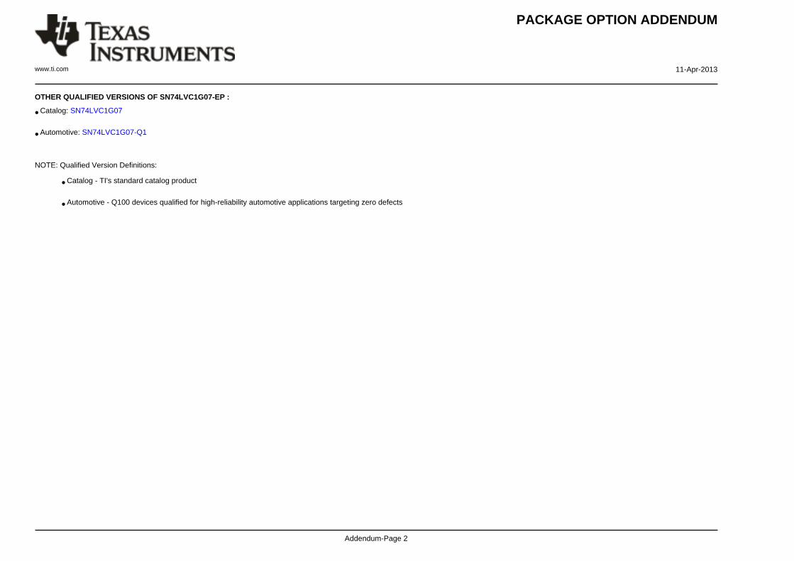
OTHER QUALIFIED VERSIONS OF SN74LVC1G07-EP :
• Catalog: SN74LVC1G07
• Automotive: SN74LVC1G07-Q1
NOTE: Qualified Version Definitions:
• Catalog - TI's standard catalog product
• Automotive - Q100 devices qualified for high-reliability automotive applications targeting zero defects
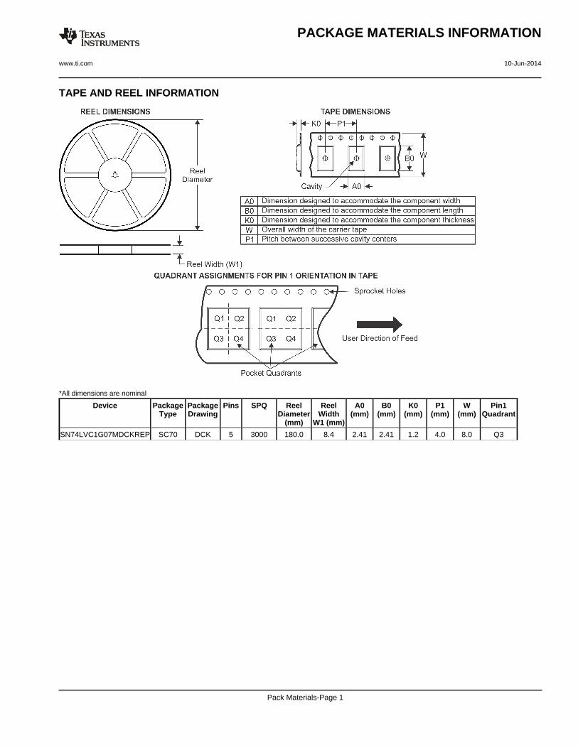
TAPE AND REEL INFORMATION
*All dimensions are nominal
Device PackageType
PackageDrawing
Pins SPQ ReelDiameter
(mm)
ReelWidth
W1 (mm)
A0(mm)
B0(mm)
K0(mm)
P1(mm)
W(mm)
Pin1Quadrant
SN74LVC1G07MDCKREP SC70 DCK 5 3000 180.0 8.4 2.41 2.41 1.2 4.0 8.0 Q3
PACKAGE MATERIALS INFORMATION
www.ti.com 10-Jun-2014
Pack Materials-Page 1
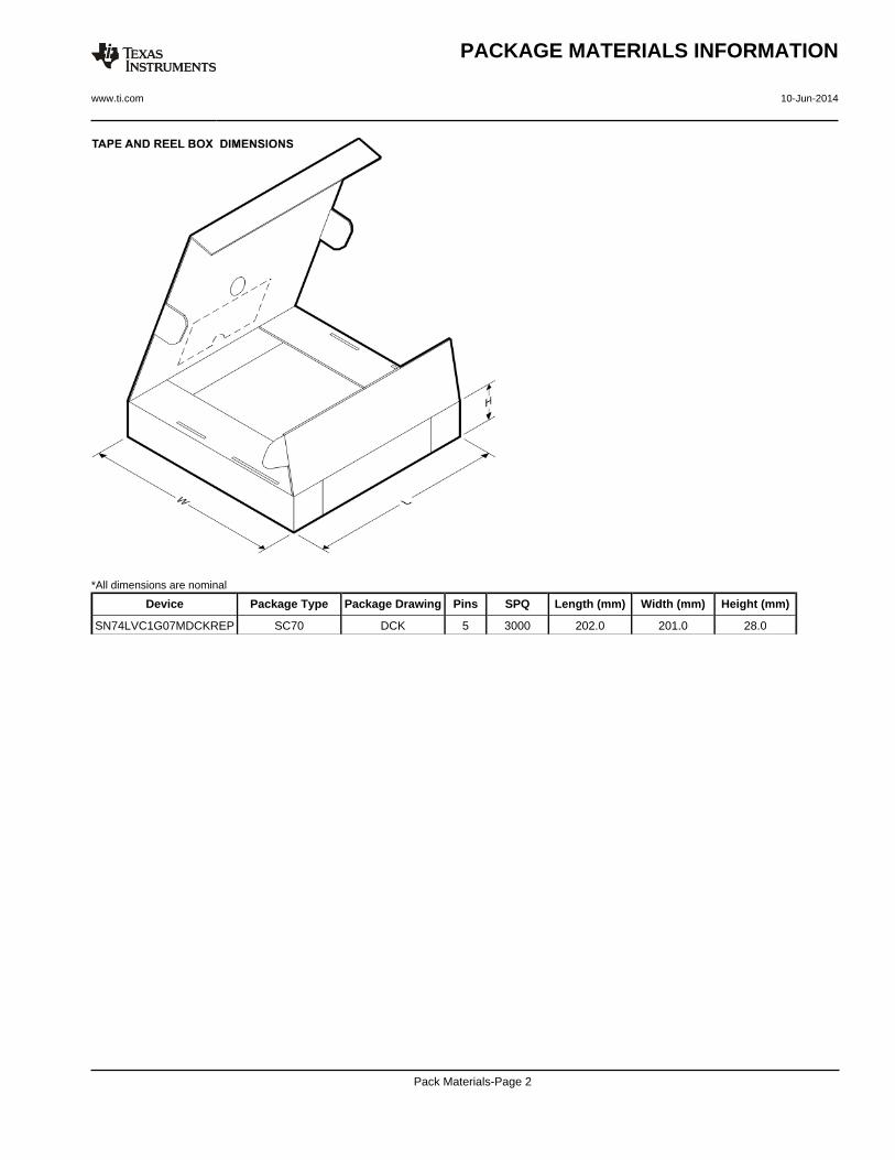
*All dimensions are nominal
Device Package Type Package Drawing Pins SPQ Length (mm) Width (mm) Height (mm)
SN74LVC1G07MDCKREP SC70 DCK 5 3000 202.0 201.0 28.0
PACKAGE MATERIALS INFORMATION
www.ti.com 10-Jun-2014
Pack Materials-Page 2
IMPORTANT NOTICETexas Instruments Incorporated and its subsidiaries (TI) reserve the right to make corrections, enhancements, improvements and otherchanges to its semiconductor products and services per JESD46, latest issue, and to discontinue any product or service per JESD48, latestissue. Buyers should obtain the latest relevant information before placing orders and should verify that such information is current andcomplete. All semiconductor products (also referred to herein as “components”) are sold subject to TI’s terms and conditions of salesupplied at the time of order acknowledgment.TI warrants performance of its components to the specifications applicable at the time of sale, in accordance with the warranty in TI’s termsand conditions of sale of semiconductor products. Testing and other quality control techniques are used to the extent TI deems necessaryto support this warranty. Except where mandated by applicable law, testing of all parameters of each component is not necessarilyperformed.TI assumes no liability for applications assistance or the design of Buyers’ products. Buyers are responsible for their products andapplications using TI components. To minimize the risks associated with Buyers’ products and applications, Buyers should provideadequate design and operating safeguards.TI does not warrant or represent that any license, either express or implied, is granted under any patent right, copyright, mask work right, orother intellectual property right relating to any combination, machine, or process in which TI components or services are used. Informationpublished by TI regarding third-party products or services does not constitute a license to use such products or services or a warranty orendorsement thereof. Use of such information may require a license from a third party under the patents or other intellectual property of thethird party, or a license from TI under the patents or other intellectual property of TI.Reproduction of significant portions of TI information in TI data books or data sheets is permissible only if reproduction is without alterationand is accompanied by all associated warranties, conditions, limitations, and notices. TI is not responsible or liable for such altereddocumentation. Information of third parties may be subject to additional restrictions.Resale of TI components or services with statements different from or beyond the parameters stated by TI for that component or servicevoids all express and any implied warranties for the associated TI component or service and is an unfair and deceptive business practice.TI is not responsible or liable for any such statements.Buyer acknowledges and agrees that it is solely responsible for compliance with all legal, regulatory and safety-related requirementsconcerning its products, and any use of TI components in its applications, notwithstanding any applications-related information or supportthat may be provided by TI. Buyer represents and agrees that it has all the necessary expertise to create and implement safeguards whichanticipate dangerous consequences of failures, monitor failures and their consequences, lessen the likelihood of failures that might causeharm and take appropriate remedial actions. Buyer will fully indemnify TI and its representatives against any damages arising out of the useof any TI components in safety-critical applications.In some cases, TI components may be promoted specifically to facilitate safety-related applications. With such components, TI’s goal is tohelp enable customers to design and create their own end-product solutions that meet applicable functional safety standards andrequirements. Nonetheless, such components are subject to these terms.No TI components are authorized for use in FDA Class III (or similar life-critical medical equipment) unless authorized officers of the partieshave executed a special agreement specifically governing such use.Only those TI components which TI has specifically designated as military grade or “enhanced plastic” are designed and intended for use inmilitary/aerospace applications or environments. Buyer acknowledges and agrees that any military or aerospace use of TI componentswhich have not been so designated is solely at the Buyer's risk, and that Buyer is solely responsible for compliance with all legal andregulatory requirements in connection with such use.TI has specifically designated certain components as meeting ISO/TS16949 requirements, mainly for automotive use. In any case of use ofnon-designated products, TI will not be responsible for any failure to meet ISO/TS16949.Products ApplicationsAudio www.ti.com/audio Automotive and Transportation www.ti.com/automotiveAmplifiers amplifier.ti.com Communications and Telecom www.ti.com/communicationsData Converters dataconverter.ti.com Computers and Peripherals www.ti.com/computersDLP® Products www.dlp.com Consumer Electronics www.ti.com/consumer-appsDSP dsp.ti.com Energy and Lighting www.ti.com/energyClocks and Timers www.ti.com/clocks Industrial www.ti.com/industrialInterface interface.ti.com Medical www.ti.com/medicalLogic logic.ti.com Security www.ti.com/securityPower Mgmt power.ti.com Space, Avionics and Defense www.ti.com/space-avionics-defenseMicrocontrollers microcontroller.ti.com Video and Imaging www.ti.com/videoRFID www.ti-rfid.comOMAP Applications Processors www.ti.com/omap TI E2E Community e2e.ti.comWireless Connectivity www.ti.com/wirelessconnectivity
Mailing Address: Texas Instruments, Post Office Box 655303, Dallas, Texas 75265Copyright © 2014, Texas Instruments Incorporated