SN74CBTLV3126 (Rev. I) - Analog, Embedded … · ˘ ˇ ˆ˙ SCDS038I − DECEMBER 1997 − REVISED...
21
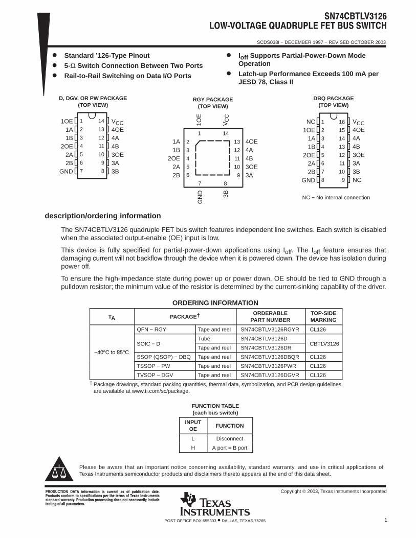
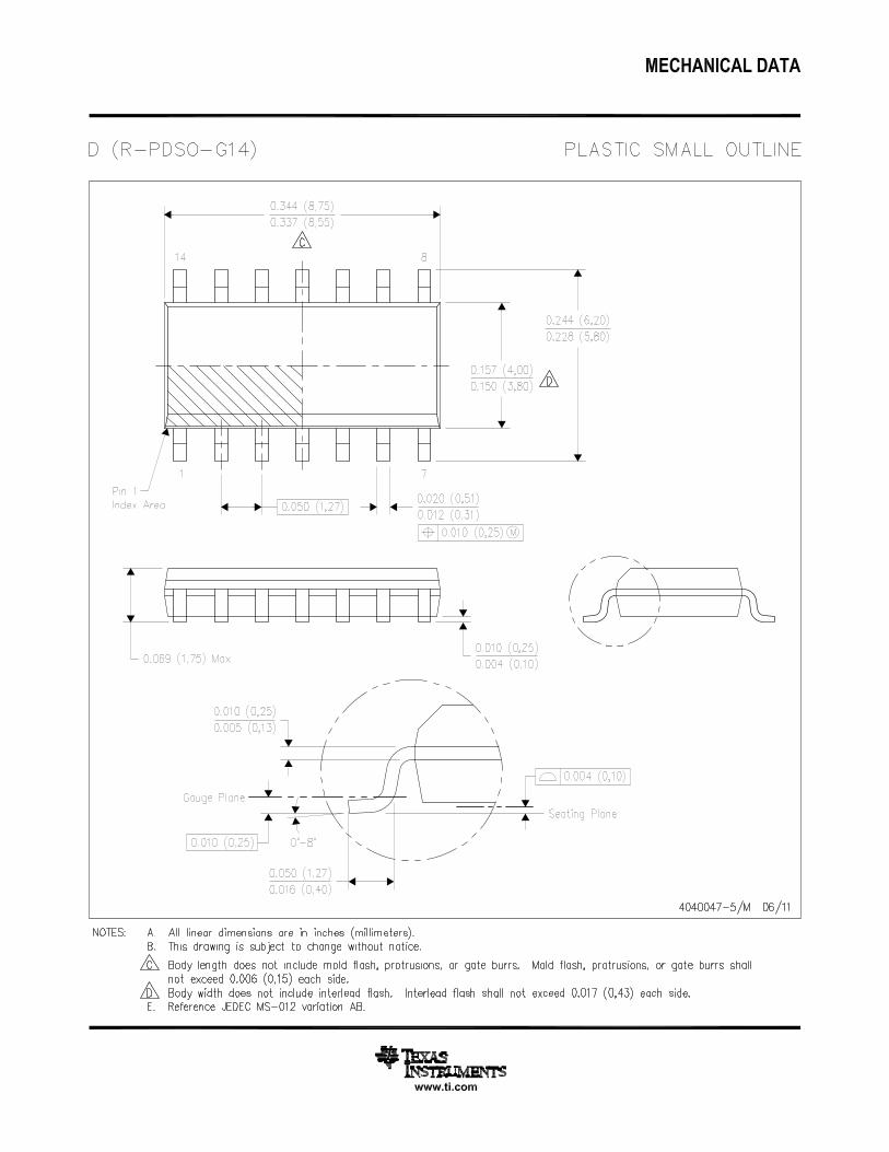
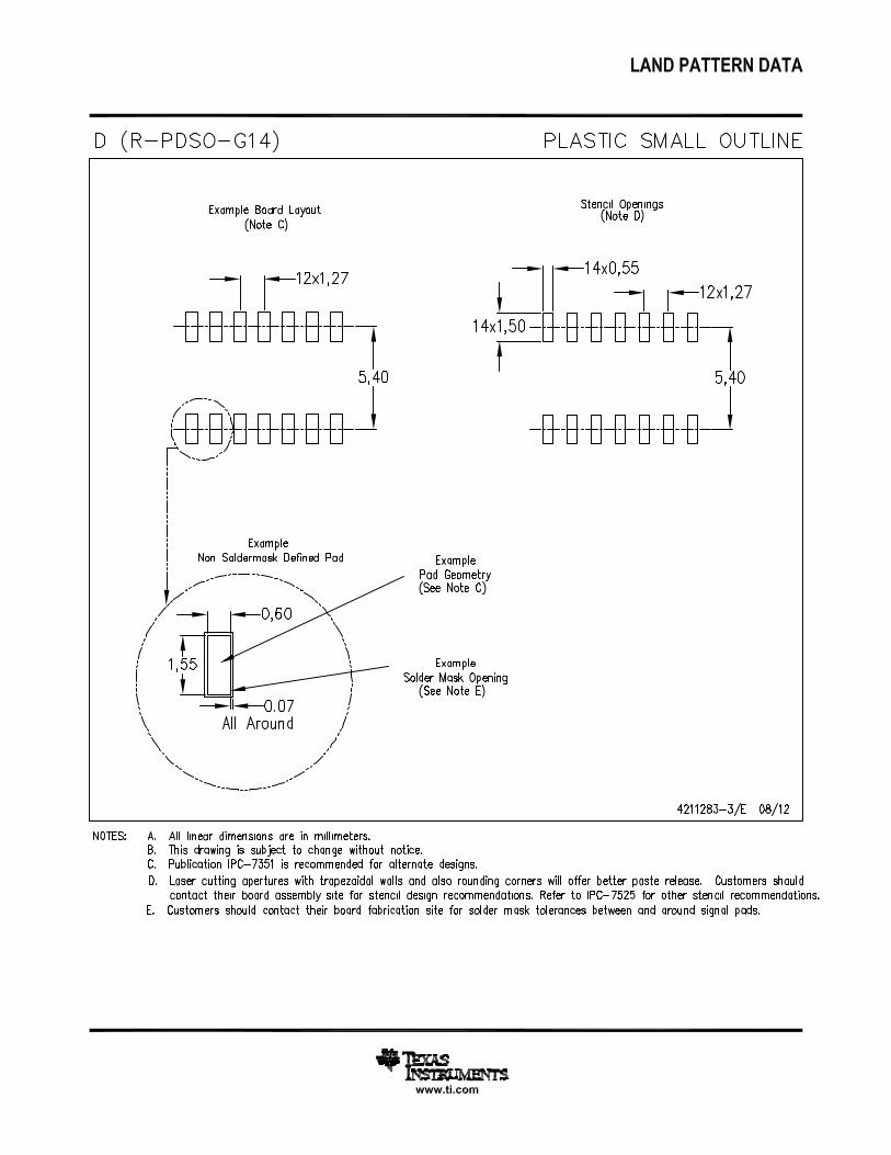
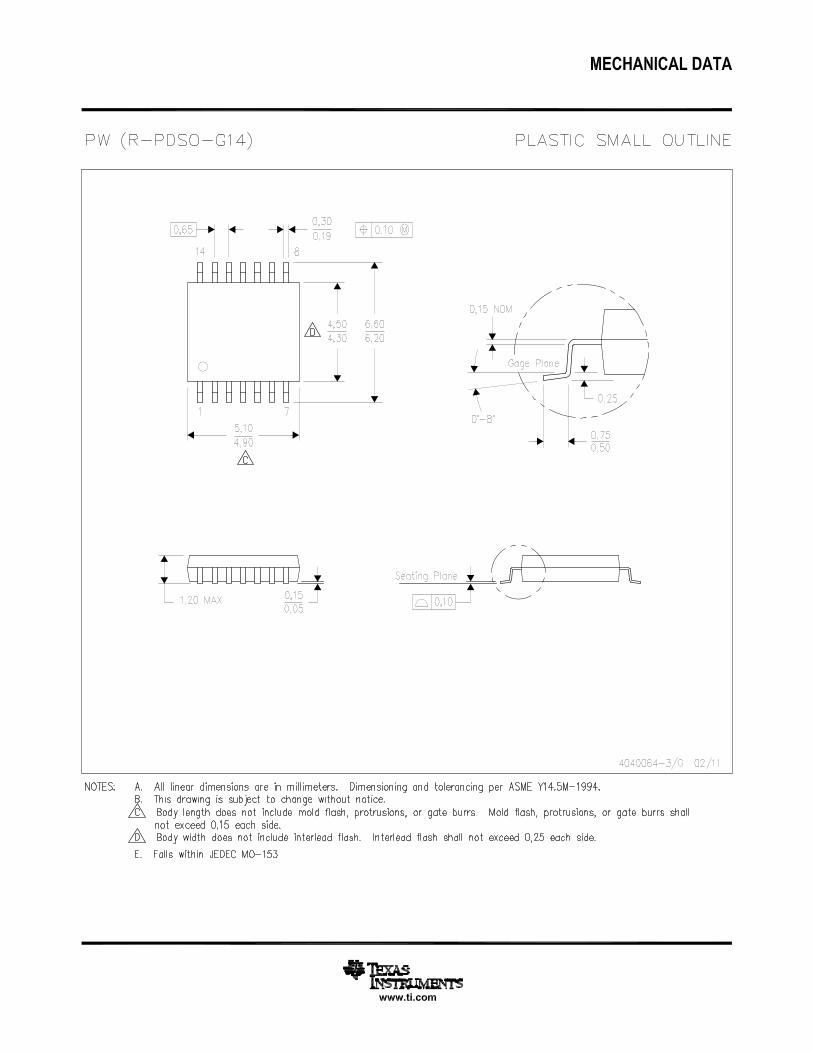
SN74CBTLV3126 LOWĆVOLTAGE QUADRUPLE FET BUS SWITCH SCDS038I - DECEMBER 1997 - REVISED OCTOBER 2003 1 POST OFFICE BOX 655303 • DALLAS, TEXAS 75265 D Standard ’126-Type Pinout D 5-Ω Switch Connection Between Two Ports D Rail-to-Rail Switching on Data I/O Ports D I off Supports Partial-Power-Down Mode Operation D Latch-up Performance Exceeds 100 mA per JESD 78, Class II 1 2 3 4 5 6 7 14 13 12 11 10 9 8 1OE 1A 1B 2OE 2A 2B GND V CC 4OE 4A 4B 3OE 3A 3B D, DGV, OR PW PACKAGE (TOP VIEW) 1 2 3 4 5 6 7 8 16 15 14 13 12 11 10 9 NC 1OE 1A 1B 2OE 2A 2B GND V CC 4OE 4A 4B 3OE 3A 3B NC DBQ PACKAGE (TOP VIEW) NC - No internal connection RGY PACKAGE (TOP VIEW) 1 14 7 8 2 3 4 5 6 13 12 11 10 9 4OE 4A 4B 3OE 3A 1A 1B 2OE 2A 2B 1OE 3B V GND CC description/ordering information The SN74CBTLV3126 quadruple FET bus switch features independent line switches. Each switch is disabled when the associated output-enable (OE) input is low. This device is fully specified for partial-power-down applications using I off . The I off feature ensures that damaging current will not backflow through the device when it is powered down. The device has isolation during power off. To ensure the high-impedance state during power up or power down, OE should be tied to GND through a pulldown resistor; the minimum value of the resistor is determined by the current-sinking capability of the driver. ORDERING INFORMATION T A PACKAGE † ORDERABLE PART NUMBER TOP-SIDE MARKING QFN - RGY Tape and reel SN74CBTLV3126RGYR CL126 SOIC - D Tube SN74CBTLV3126D CBTLV3126 -40°C to 85°C SOIC - D Tape and reel SN74CBTLV3126DR CBTLV3126 -40°C to 85°C SSOP (QSOP) - DBQ Tape and reel SN74CBTLV3126DBQR CL126 TSSOP - PW Tape and reel SN74CBTLV3126PWR CL126 TVSOP - DGV Tape and reel SN74CBTLV3126DGVR CL126 † Package drawings, standard packing quantities, thermal data, symbolization, and PCB design guidelines are available at www.ti.com/sc/package. FUNCTION TABLE (each bus switch) INPUT OE FUNCTION L Disconnect H A port = B port Copyright 2003, Texas Instruments Incorporated PRODUCTION DATA information is current as of publication date. Products conform to specifications per the terms of Texas Instruments standard warranty. Production processing does not necessarily include testing of all parameters. Please be aware that an important notice concerning availability, standard warranty, and use in critical applications of Texas Instruments semiconductor products and disclaimers thereto appears at the end of this data sheet.
Transcript of SN74CBTLV3126 (Rev. I) - Analog, Embedded … · ˘ ˇ ˆ˙ SCDS038I − DECEMBER 1997 − REVISED...
SCDS038I − DECEMBER 1997 − REVISED OCTOBER 2003
1POST OFFICE BOX 655303 • DALLAS, TEXAS 75265
Standard ’126-Type Pinout
5-Ω Switch Connection Between Two Ports
Rail-to-Rail Switching on Data I/O Ports
Ioff Supports Partial-Power-Down ModeOperation
Latch-up Performance Exceeds 100 mA perJESD 78, Class II
1
2
3
4
5
6
7
14
13
12
11
10
9
8
1OE1A1B
2OE2A2B
GND
VCC4OE4A4B3OE3A3B
D, DGV, OR PW PACKAGE(TOP VIEW)
1
2
3
4
5
6
7
8
16
15
14
13
12
11
10
9
NC1OE
1A1B
2OE2A2B
GND
VCC4OE4A4B3OE3A3BNC
DBQ PACKAGE(TOP VIEW)
NC − No internal connection
RGY PACKAGE(TOP VIEW)
1 14
7 8
2
3
4
5
6
13
12
11
10
9
4OE4A4B3OE3A
1A1B
2OE2A2B
1OE
3BV
GN
D
CC
description/ordering information
The SN74CBTLV3126 quadruple FET bus switch features independent line switches. Each switch is disabledwhen the associated output-enable (OE) input is low.
This device is fully specified for partial-power-down applications using Ioff. The Ioff feature ensures thatdamaging current will not backflow through the device when it is powered down. The device has isolation duringpower off.
To ensure the high-impedance state during power up or power down, OE should be tied to GND through apulldown resistor; the minimum value of the resistor is determined by the current-sinking capability of the driver.
ORDERING INFORMATION
TA PACKAGE † ORDERABLEPART NUMBER
TOP-SIDEMARKING
QFN − RGY Tape and reel SN74CBTLV3126RGYR CL126
SOIC − DTube SN74CBTLV3126D
CBTLV3126
−40°C to 85°CSOIC − D
Tape and reel SN74CBTLV3126DRCBTLV3126
−40°C to 85°CSSOP (QSOP) − DBQ Tape and reel SN74CBTLV3126DBQR CL126
TSSOP − PW Tape and reel SN74CBTLV3126PWR CL126
TVSOP − DGV Tape and reel SN74CBTLV3126DGVR CL126
† Package drawings, standard packing quantities, thermal data, symbolization, and PCB design guidelinesare available at www.ti.com/sc/package.
FUNCTION TABLE(each bus switch)
INPUTOE FUNCTION
L Disconnect
H A port = B port
Copyright 2003, Texas Instruments Incorporated !"#$ % &'!!($ #% )'*+&#$ ,#$(-!,'&$% &!" $ %)(&&#$% )(! $.( $(!"% (/#% %$!'"($%%$#,#!, 0#!!#$1- !,'&$ )!&(%%2 ,(% $ (&(%%#!+1 &+',($(%$2 #++ )#!#"($(!%-
Please be aware that an important notice concerning availability, standard warranty, and use in critical applications ofTexas Instruments semiconductor products and disclaimers thereto appears at the end of this data sheet.
SCDS038I − DECEMBER 1997 − REVISED OCTOBER 2003
2 POST OFFICE BOX 655303 • DALLAS, TEXAS 75265
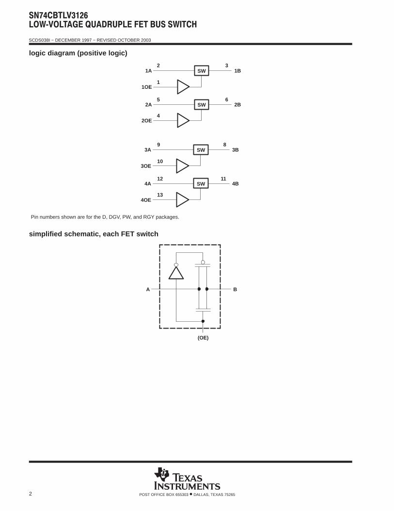
logic diagram (positive logic)
1A
1OE
SW 1B
2A
2OE
SW 2B
3A
3OE
SW 3B
4A
4OE
SW 4B
2
1
5
4
9
10
12
13
3
6
8
11
Pin numbers shown are for the D, DGV, PW, and RGY packages.
simplified schematic, each FET switch
A
(OE)
B
SCDS038I − DECEMBER 1997 − REVISED OCTOBER 2003
3POST OFFICE BOX 655303 • DALLAS, TEXAS 75265
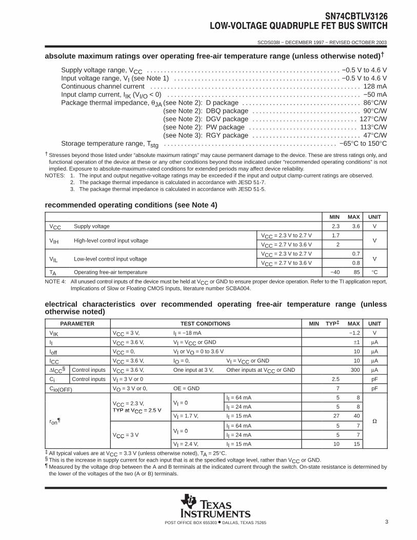
absolute maximum ratings over operating free-air temperature range (unless otherwise noted) †
Supply voltage range, VCC −0.5 V to 4.6 V. . . . . . . . . . . . . . . . . . . . . . . . . . . . . . . . . . . . . . . . . . . . . . . . . . . . . . . . . Input voltage range, VI (see Note 1) −0.5 V to 4.6 V. . . . . . . . . . . . . . . . . . . . . . . . . . . . . . . . . . . . . . . . . . . . . . . . . Continuous channel current 128 mA. . . . . . . . . . . . . . . . . . . . . . . . . . . . . . . . . . . . . . . . . . . . . . . . . . . . . . . . . . . . . . Input clamp current, IIK (VI/O < 0) −50 mA. . . . . . . . . . . . . . . . . . . . . . . . . . . . . . . . . . . . . . . . . . . . . . . . . . . . . . . . . Package thermal impedance, θJA (see Note 2): D package 86°C/W. . . . . . . . . . . . . . . . . . . . . . . . . . . . . . . . . . .
(see Note 2): DBQ package 90°C/W. . . . . . . . . . . . . . . . . . . . . . . . . . . . . . . . (see Note 2): DGV package 127°C/W. . . . . . . . . . . . . . . . . . . . . . . . . . . . . . . (see Note 2): PW package 113°C/W. . . . . . . . . . . . . . . . . . . . . . . . . . . . . . . . (see Note 3): RGY package 47°C/W. . . . . . . . . . . . . . . . . . . . . . . . . . . . . . . .
Storage temperature range, Tstg −65°C to 150°C. . . . . . . . . . . . . . . . . . . . . . . . . . . . . . . . . . . . . . . . . . . . . . . . . . .
† Stresses beyond those listed under “absolute maximum ratings” may cause permanent damage to the device. These are stress ratings only, andfunctional operation of the device at these or any other conditions beyond those indicated under “recommended operating conditions” is notimplied. Exposure to absolute-maximum-rated conditions for extended periods may affect device reliability.
NOTES: 1. The input and output negative-voltage ratings may be exceeded if the input and output clamp-current ratings are observed.2. The package thermal impedance is calculated in accordance with JESD 51-7.3. The package thermal impedance is calculated in accordance with JESD 51-5.
recommended operating conditions (see Note 4)
MIN MAX UNIT
VCC Supply voltage 2.3 3.6 V
VIH High-level control input voltageVCC = 2.3 V to 2.7 V 1.7
VVIH High-level control input voltageVCC = 2.7 V to 3.6 V 2
V
VIL Low-level control input voltageVCC = 2.3 V to 2.7 V 0.7
VVIL Low-level control input voltageVCC = 2.7 V to 3.6 V 0.8
V
TA Operating free-air temperature −40 85 °C
NOTE 4: All unused control inputs of the device must be held at VCC or GND to ensure proper device operation. Refer to the TI application report,Implications of Slow or Floating CMOS Inputs, literature number SCBA004.
electrical characteristics over recommended operating free-air temperature range (unlessotherwise noted)
PARAMETER TEST CONDITIONS MIN TYP‡ MAX UNIT
VIK VCC = 3 V, II = −18 mA −1.2 V
II VCC = 3.6 V, VI = VCC or GND ±1 µA
Ioff VCC = 0, VI or VO = 0 to 3.6 V 10 µA
ICC VCC = 3.6 V, IO = 0, VI = VCC or GND 10 µA
∆ICC§ Control inputs VCC = 3.6 V, One input at 3 V, Other inputs at VCC or GND 300 µA
Ci Control inputs VI = 3 V or 0 2.5 pF
Cio(OFF) VO = 3 V or 0, OE = GND 7 pF
VCC = 2.3 V, VI = 0II = 64 mA 5 8
VCC = 2.3 V,TYP at VCC = 2.5 V
VI = 0II = 24 mA 5 8
ron¶
TYP at VCC = 2.5 VVI = 1.7 V, II = 15 mA 27 40
Ωron¶
VI = 0II = 64 mA 5 7
Ω
VCC = 3 VVI = 0
II = 24 mA 5 7VCC = 3 V
VI = 2.4 V, II = 15 mA 10 15
‡ All typical values are at VCC = 3.3 V (unless otherwise noted), TA = 25°C.§ This is the increase in supply current for each input that is at the specified voltage level, rather than VCC or GND.¶ Measured by the voltage drop between the A and B terminals at the indicated current through the switch. On-state resistance is determined by
the lower of the voltages of the two (A or B) terminals.
SCDS038I − DECEMBER 1997 − REVISED OCTOBER 2003
4 POST OFFICE BOX 655303 • DALLAS, TEXAS 75265
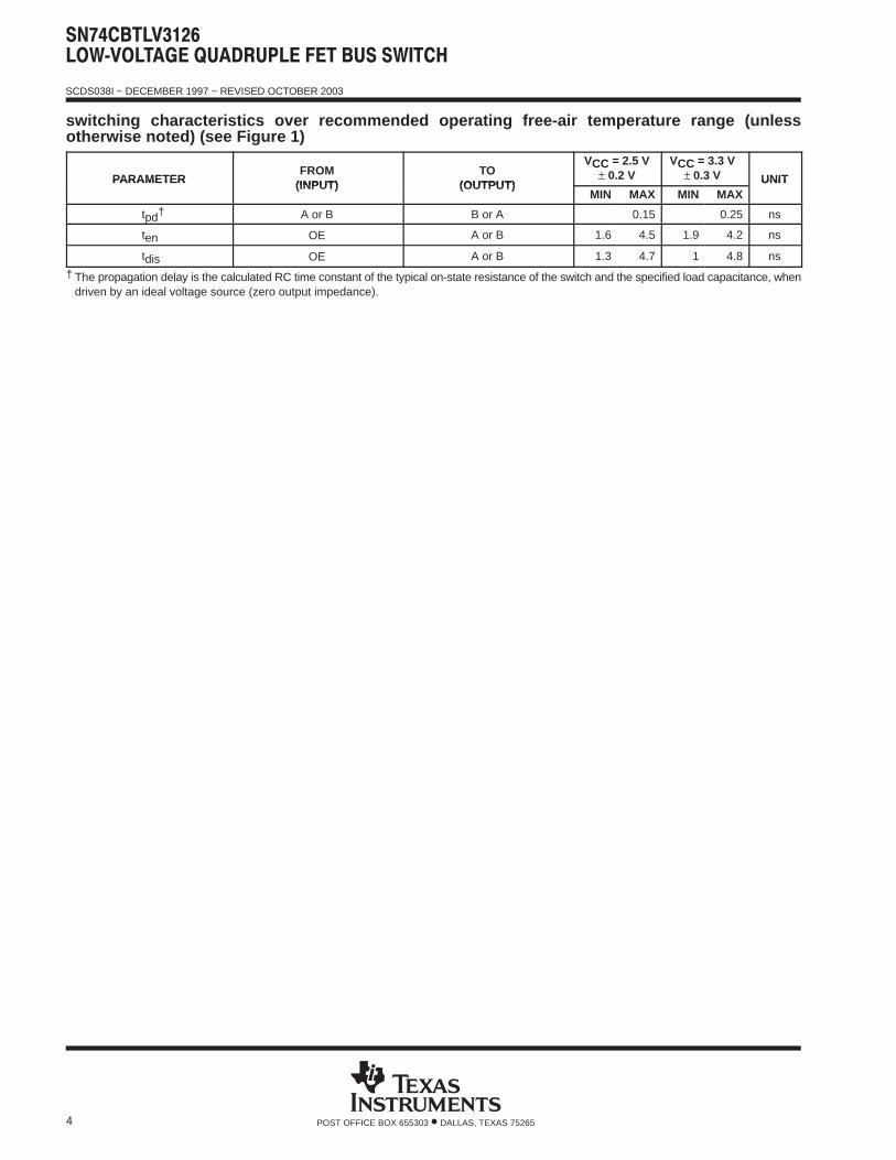
switching characteristics over recommended operating free-air temperature range (unlessotherwise noted) (see Figure 1)
PARAMETERFROM
(INPUT)TO
(OUTPUT)
VCC = 2.5 V± 0.2 V
VCC = 3.3 V± 0.3 V UNITPARAMETER (INPUT) (OUTPUT)
MIN MAX MIN MAXUNIT
tpd† A or B B or A 0.15 0.25 ns
ten OE A or B 1.6 4.5 1.9 4.2 ns
tdis OE A or B 1.3 4.7 1 4.8 ns
† The propagation delay is the calculated RC time constant of the typical on-state resistance of the switch and the specified load capacitance, whendriven by an ideal voltage source (zero output impedance).
SCDS038I − DECEMBER 1997 − REVISED OCTOBER 2003
5POST OFFICE BOX 655303 • DALLAS, TEXAS 75265
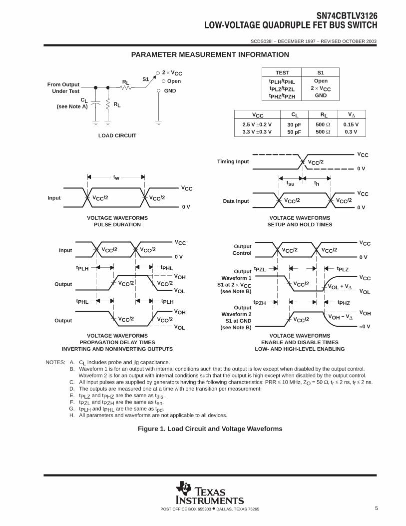
PARAMETER MEASUREMENT INFORMATION
VCC/2
thtsu
From OutputUnder Test
CL(see Note A)
LOAD CIRCUIT
S12 × VCC
Open
GND
RL
RL
Data Input
Timing InputVCC
0 V
VCC
0 V0 V
tw
Input
VOLTAGE WAVEFORMSSETUP AND HOLD TIMES
VOLTAGE WAVEFORMSPROPAGATION DELAY TIMES
INVERTING AND NONINVERTING OUTPUTS
VOLTAGE WAVEFORMSPULSE DURATION
tPLH
tPHL
tPHL
tPLH
VOH
VOH
VOL
VOL
VCC
0 VInput
OutputWaveform 1
S1 at 2 × VCC(see Note B)
OutputWaveform 2
S1 at GND(see Note B)
VOL
VOH
tPZL
tPZH
tPLZ
tPHZ
VCC
0 V
VOL + V∆
VOH − V∆
≈0 V
VCC
VOLTAGE WAVEFORMSENABLE AND DISABLE TIMES
LOW- AND HIGH-LEVEL ENABLING
Output
Output
tPLH/tPHLtPLZ/tPZLtPHZ/tPZH
Open2 × VCC
GND
TEST S1
NOTES: A. CL includes probe and jig capacitance.B. Waveform 1 is for an output with internal conditions such that the output is low except when disabled by the output control.
Waveform 2 is for an output with internal conditions such that the output is high except when disabled by the output control.C. All input pulses are supplied by generators having the following characteristics: PRR ≤ 10 MHz, ZO = 50 Ω, tr ≤ 2 ns, tf ≤ 2 ns.D. The outputs are measured one at a time with one transition per measurement.E. tPLZ and tPHZ are the same as tdis.F. tPZL and tPZH are the same as ten.G. tPLH and tPHL are the same as tpd.H. All parameters and waveforms are not applicable to all devices.
OutputControl
VCC/2 VCC/2
VCC/2 VCC/2
VCC/2 VCC/2
VCC/2
VCC/2 VCC/2
VCC/2
VCC/2
VCC/2
VCC
VCC/2
VCC/2
2.5 V ±0.2 V3.3 V ±0.3 V
500 Ω500 Ω
VCC RL
0.15 V0.3 V
V∆CL
30 pF50 pF
Figure 1. Load Circuit and Voltage Waveforms
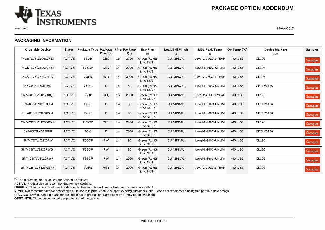
PACKAGE OPTION ADDENDUM
www.ti.com 15-Apr-2017
Addendum-Page 1
PACKAGING INFORMATION
Orderable Device Status(1)
Package Type PackageDrawing
Pins PackageQty
Eco Plan(2)
Lead/Ball Finish(6)
MSL Peak Temp(3)
Op Temp (°C) Device Marking(4/5)
Samples
74CBTLV3126DBQRE4 ACTIVE SSOP DBQ 16 2500 Green (RoHS& no Sb/Br)
CU NIPDAU Level-2-260C-1 YEAR -40 to 85 CL126
74CBTLV3126DGVRE4 ACTIVE TVSOP DGV 14 2000 Green (RoHS& no Sb/Br)
CU NIPDAU Level-1-260C-UNLIM -40 to 85 CL126
74CBTLV3126RGYRG4 ACTIVE VQFN RGY 14 3000 Green (RoHS& no Sb/Br)
CU NIPDAU Level-2-260C-1 YEAR -40 to 85 CL126
SN74CBTLV3126D ACTIVE SOIC D 14 50 Green (RoHS& no Sb/Br)
CU NIPDAU Level-1-260C-UNLIM -40 to 85 CBTLV3126
SN74CBTLV3126DBQR ACTIVE SSOP DBQ 16 2500 Green (RoHS& no Sb/Br)
CU NIPDAU Level-2-260C-1 YEAR -40 to 85 CL126
SN74CBTLV3126DE4 ACTIVE SOIC D 14 50 Green (RoHS& no Sb/Br)
CU NIPDAU Level-1-260C-UNLIM -40 to 85 CBTLV3126
SN74CBTLV3126DG4 ACTIVE SOIC D 14 50 Green (RoHS& no Sb/Br)
CU NIPDAU Level-1-260C-UNLIM -40 to 85 CBTLV3126
SN74CBTLV3126DGVR ACTIVE TVSOP DGV 14 2000 Green (RoHS& no Sb/Br)
CU NIPDAU Level-1-260C-UNLIM -40 to 85 CL126
SN74CBTLV3126DR ACTIVE SOIC D 14 2500 Green (RoHS& no Sb/Br)
CU NIPDAU Level-1-260C-UNLIM -40 to 85 CBTLV3126
SN74CBTLV3126PW ACTIVE TSSOP PW 14 90 Green (RoHS& no Sb/Br)
CU NIPDAU Level-1-260C-UNLIM -40 to 85 CL126
SN74CBTLV3126PWG4 ACTIVE TSSOP PW 14 90 Green (RoHS& no Sb/Br)
CU NIPDAU Level-1-260C-UNLIM -40 to 85 CL126
SN74CBTLV3126PWR ACTIVE TSSOP PW 14 2000 Green (RoHS& no Sb/Br)
CU NIPDAU Level-1-260C-UNLIM -40 to 85 CL126
SN74CBTLV3126RGYR ACTIVE VQFN RGY 14 3000 Green (RoHS& no Sb/Br)
CU NIPDAU Level-2-260C-1 YEAR -40 to 85 CL126
(1) The marketing status values are defined as follows:ACTIVE: Product device recommended for new designs.LIFEBUY: TI has announced that the device will be discontinued, and a lifetime-buy period is in effect.NRND: Not recommended for new designs. Device is in production to support existing customers, but TI does not recommend using this part in a new design.PREVIEW: Device has been announced but is not in production. Samples may or may not be available.OBSOLETE: TI has discontinued the production of the device.
PACKAGE OPTION ADDENDUM
www.ti.com 15-Apr-2017
Addendum-Page 2
(2) Eco Plan - The planned eco-friendly classification: Pb-Free (RoHS), Pb-Free (RoHS Exempt), or Green (RoHS & no Sb/Br) - please check http://www.ti.com/productcontent for the latest availabilityinformation and additional product content details.TBD: The Pb-Free/Green conversion plan has not been defined.Pb-Free (RoHS): TI's terms "Lead-Free" or "Pb-Free" mean semiconductor products that are compatible with the current RoHS requirements for all 6 substances, including the requirement thatlead not exceed 0.1% by weight in homogeneous materials. Where designed to be soldered at high temperatures, TI Pb-Free products are suitable for use in specified lead-free processes.Pb-Free (RoHS Exempt): This component has a RoHS exemption for either 1) lead-based flip-chip solder bumps used between the die and package, or 2) lead-based die adhesive used betweenthe die and leadframe. The component is otherwise considered Pb-Free (RoHS compatible) as defined above.Green (RoHS & no Sb/Br): TI defines "Green" to mean Pb-Free (RoHS compatible), and free of Bromine (Br) and Antimony (Sb) based flame retardants (Br or Sb do not exceed 0.1% by weightin homogeneous material)
(3) MSL, Peak Temp. - The Moisture Sensitivity Level rating according to the JEDEC industry standard classifications, and peak solder temperature.
(4) There may be additional marking, which relates to the logo, the lot trace code information, or the environmental category on the device.
(5) Multiple Device Markings will be inside parentheses. Only one Device Marking contained in parentheses and separated by a "~" will appear on a device. If a line is indented then it is a continuationof the previous line and the two combined represent the entire Device Marking for that device.
(6) Lead/Ball Finish - Orderable Devices may have multiple material finish options. Finish options are separated by a vertical ruled line. Lead/Ball Finish values may wrap to two lines if the finishvalue exceeds the maximum column width.
Important Information and Disclaimer:The information provided on this page represents TI's knowledge and belief as of the date that it is provided. TI bases its knowledge and belief on informationprovided by third parties, and makes no representation or warranty as to the accuracy of such information. Efforts are underway to better integrate information from third parties. TI has taken andcontinues to take reasonable steps to provide representative and accurate information but may not have conducted destructive testing or chemical analysis on incoming materials and chemicals.TI and TI suppliers consider certain information to be proprietary, and thus CAS numbers and other limited information may not be available for release.
In no event shall TI's liability arising out of such information exceed the total purchase price of the TI part(s) at issue in this document sold by TI to Customer on an annual basis.
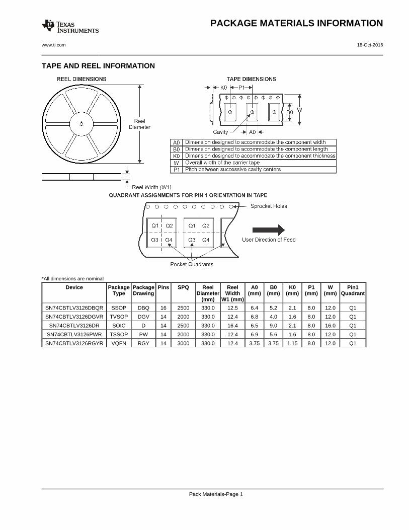
TAPE AND REEL INFORMATION
*All dimensions are nominal
Device PackageType
PackageDrawing
Pins SPQ ReelDiameter
(mm)
ReelWidth
W1 (mm)
A0(mm)
B0(mm)
K0(mm)
P1(mm)
W(mm)
Pin1Quadrant
SN74CBTLV3126DBQR SSOP DBQ 16 2500 330.0 12.5 6.4 5.2 2.1 8.0 12.0 Q1
SN74CBTLV3126DGVR TVSOP DGV 14 2000 330.0 12.4 6.8 4.0 1.6 8.0 12.0 Q1
SN74CBTLV3126DR SOIC D 14 2500 330.0 16.4 6.5 9.0 2.1 8.0 16.0 Q1
SN74CBTLV3126PWR TSSOP PW 14 2000 330.0 12.4 6.9 5.6 1.6 8.0 12.0 Q1
SN74CBTLV3126RGYR VQFN RGY 14 3000 330.0 12.4 3.75 3.75 1.15 8.0 12.0 Q1
PACKAGE MATERIALS INFORMATION
www.ti.com 18-Oct-2016
Pack Materials-Page 1
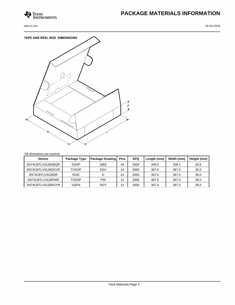
*All dimensions are nominal
Device Package Type Package Drawing Pins SPQ Length (mm) Width (mm) Height (mm)
SN74CBTLV3126DBQR SSOP DBQ 16 2500 340.5 338.1 20.6
SN74CBTLV3126DGVR TVSOP DGV 14 2000 367.0 367.0 35.0
SN74CBTLV3126DR SOIC D 14 2500 367.0 367.0 38.0
SN74CBTLV3126PWR TSSOP PW 14 2000 367.0 367.0 35.0
SN74CBTLV3126RGYR VQFN RGY 14 3000 367.0 367.0 35.0
PACKAGE MATERIALS INFORMATION
www.ti.com 18-Oct-2016
Pack Materials-Page 2
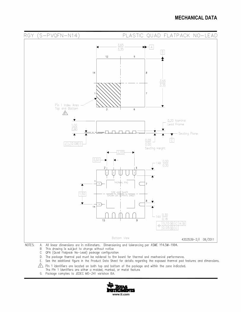
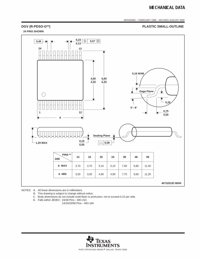
MECHANICAL DATA
MPDS006C – FEBRUARY 1996 – REVISED AUGUST 2000
POST OFFICE BOX 655303 • DALLAS, TEXAS 75265
DGV (R-PDSO-G**) PLASTIC SMALL-OUTLINE 24 PINS SHOWN
14
3,70
3,50 4,90
5,10
20DIM
PINS **
4073251/E 08/00
1,20 MAX
Seating Plane
0,050,15
0,25
0,500,75
0,230,13
1 12
24 13
4,304,50
0,16 NOM
Gage Plane
A
7,90
7,70
382416
4,90
5,103,70
3,50
A MAX
A MIN
6,606,20
11,20
11,40
56
9,60
9,80
48
0,08
M0,070,40
0°–8°
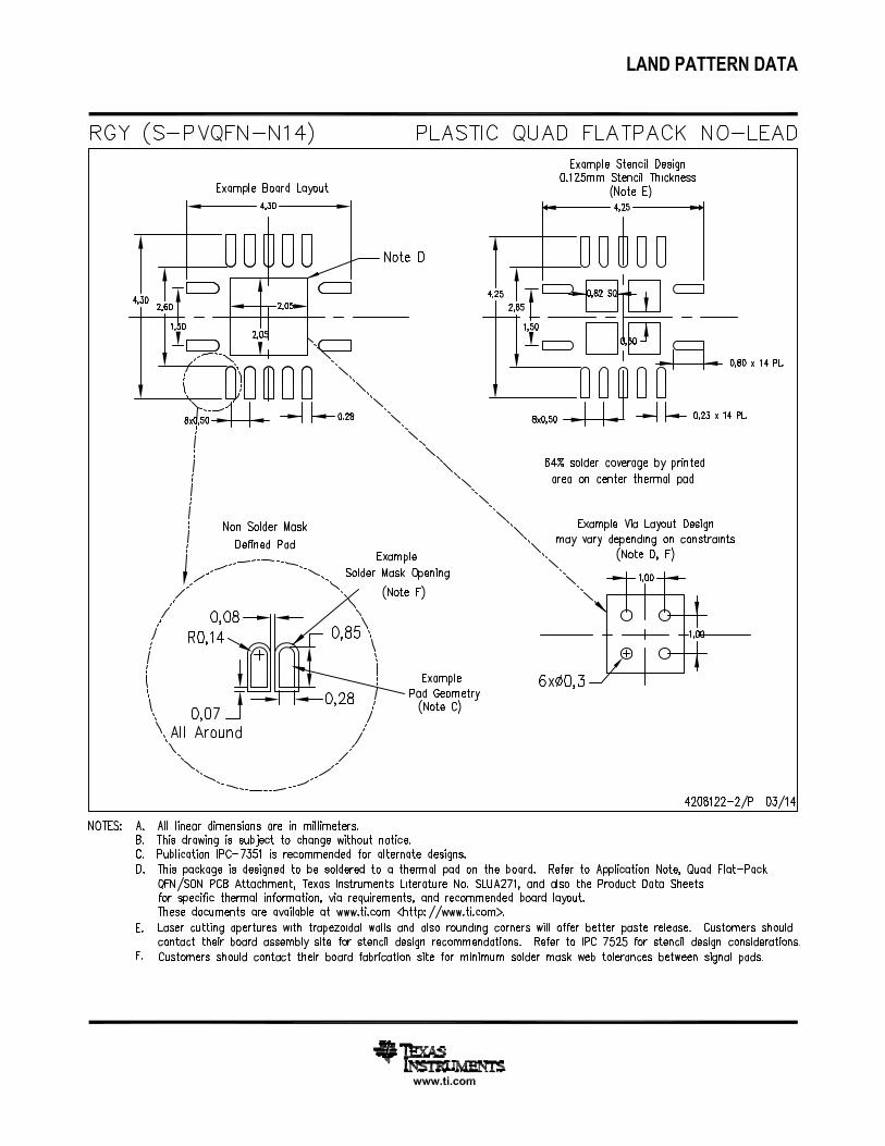
NOTES: A. All linear dimensions are in millimeters.B. This drawing is subject to change without notice.C. Body dimensions do not include mold flash or protrusion, not to exceed 0,15 per side.D. Falls within JEDEC: 24/48 Pins – MO-153
14/16/20/56 Pins – MO-194
www.ti.com
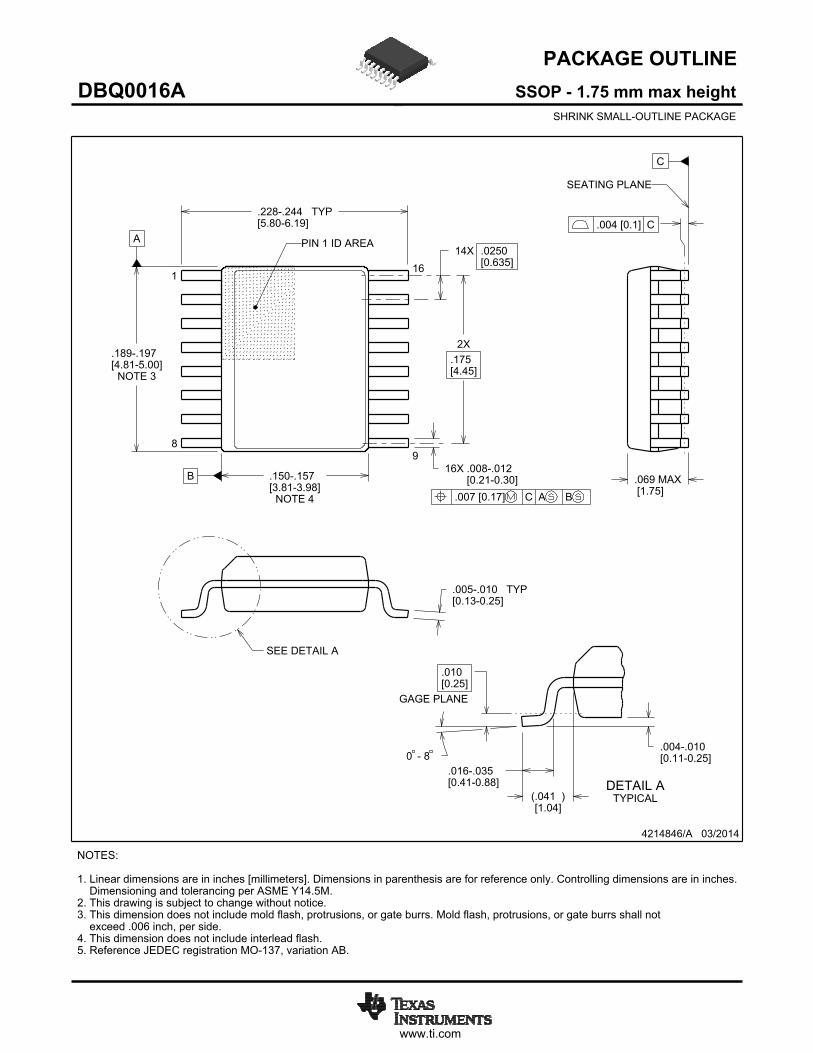
PACKAGE OUTLINE
C
TYP-.244.228-6.195.80[ ]
.069 MAX[1.75]
14X .0250[0.635]
16X -.012.008-0.300.21[ ]
2X.175[4.45]
TYP-.010.005-0.250.13[ ]
0 - 8-.010.004-0.250.11[ ]
(.041 )[1.04]
.010[0.25]
GAGE PLANE
-.035.016-0.880.41[ ]
A
NOTE 3
-.197.189-5.004.81[ ]
B
NOTE 4
-.157.150-3.983.81[ ]
SSOP - 1.75 mm max heightDBQ0016ASHRINK SMALL-OUTLINE PACKAGE
4214846/A 03/2014
NOTES: 1. Linear dimensions are in inches [millimeters]. Dimensions in parenthesis are for reference only. Controlling dimensions are in inches. Dimensioning and tolerancing per ASME Y14.5M. 2. This drawing is subject to change without notice. 3. This dimension does not include mold flash, protrusions, or gate burrs. Mold flash, protrusions, or gate burrs shall not exceed .006 inch, per side. 4. This dimension does not include interlead flash.5. Reference JEDEC registration MO-137, variation AB.
116
.007 [0.17] C A B
98
PIN 1 ID AREA
SEATING PLANE
.004 [0.1] C
SEE DETAIL A
DETAIL ATYPICAL
SCALE 2.800
www.ti.com
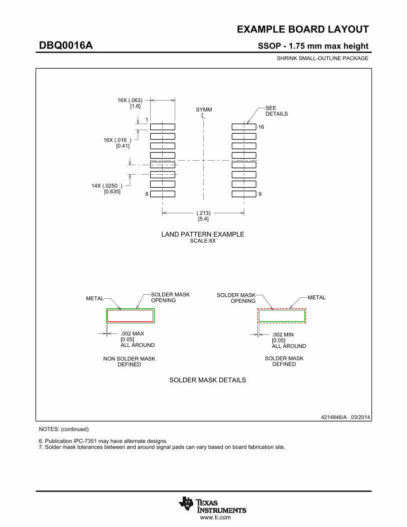
EXAMPLE BOARD LAYOUT
.002 MAX[0.05]ALL AROUND
.002 MIN[0.05]ALL AROUND
(.213)[5.4]
14X (.0250 )[0.635]
16X (.063)[1.6]
16X (.016 )[0.41]
SSOP - 1.75 mm max heightDBQ0016ASHRINK SMALL-OUTLINE PACKAGE
4214846/A 03/2014
NOTES: (continued) 6. Publication IPC-7351 may have alternate designs. 7. Solder mask tolerances between and around signal pads can vary based on board fabrication site.
METALSOLDER MASKOPENING
NON SOLDER MASKDEFINED
SOLDER MASK DETAILS
OPENINGSOLDER MASK METAL
SOLDER MASKDEFINED
LAND PATTERN EXAMPLESCALE:8X
SYMM
1
8 9
16
SEEDETAILS
www.ti.com
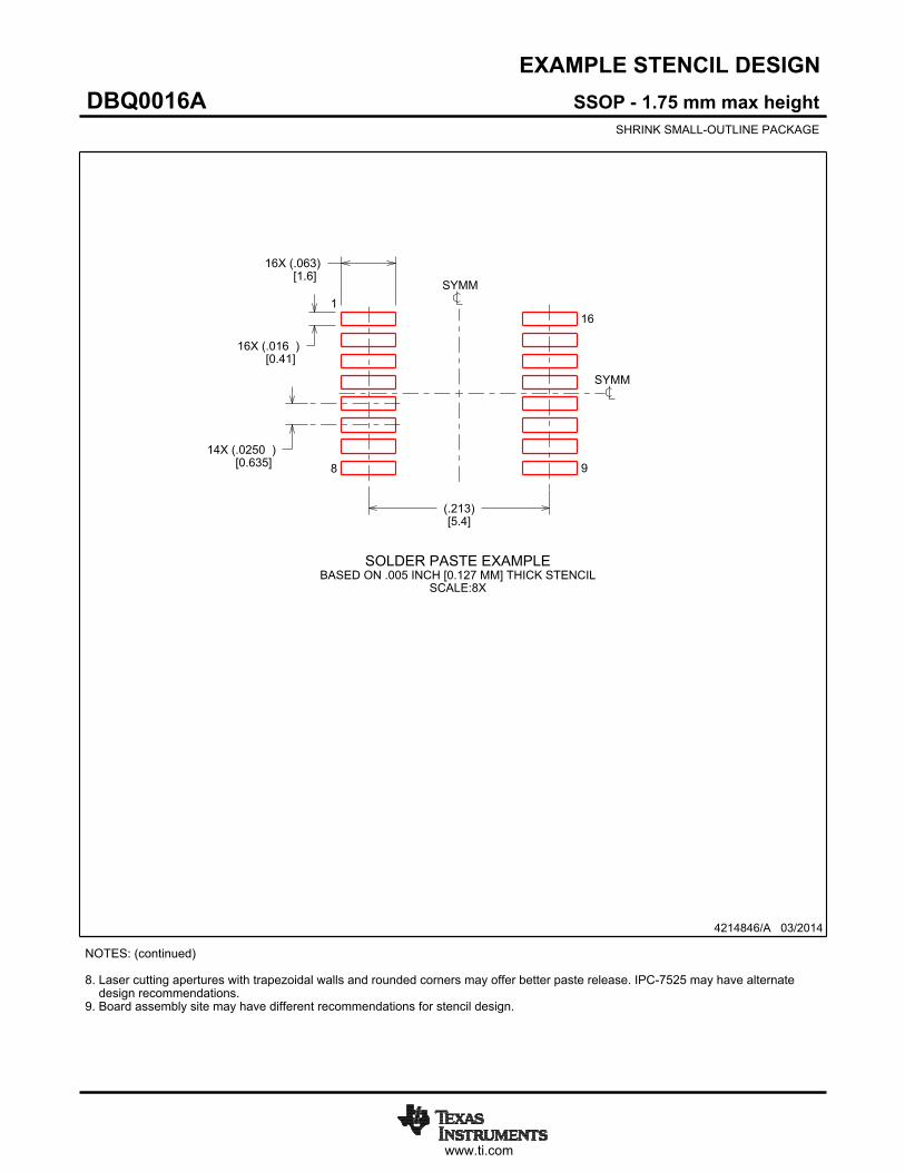
EXAMPLE STENCIL DESIGN
16X (.063)[1.6]
16X (.016 )[0.41]
14X (.0250 )[0.635]
(.213)[5.4]
SSOP - 1.75 mm max heightDBQ0016ASHRINK SMALL-OUTLINE PACKAGE
4214846/A 03/2014
NOTES: (continued) 8. Laser cutting apertures with trapezoidal walls and rounded corners may offer better paste release. IPC-7525 may have alternate design recommendations. 9. Board assembly site may have different recommendations for stencil design.
SOLDER PASTE EXAMPLEBASED ON .005 INCH [0.127 MM] THICK STENCIL
SCALE:8X
SYMM
SYMM
1
8 9
16
IMPORTANT NOTICE
Texas Instruments Incorporated (TI) reserves the right to make corrections, enhancements, improvements and other changes to itssemiconductor products and services per JESD46, latest issue, and to discontinue any product or service per JESD48, latest issue. Buyersshould obtain the latest relevant information before placing orders and should verify that such information is current and complete.TI’s published terms of sale for semiconductor products (http://www.ti.com/sc/docs/stdterms.htm) apply to the sale of packaged integratedcircuit products that TI has qualified and released to market. Additional terms may apply to the use or sale of other types of TI products andservices.Reproduction of significant portions of TI information in TI data sheets is permissible only if reproduction is without alteration and isaccompanied by all associated warranties, conditions, limitations, and notices. TI is not responsible or liable for such reproduceddocumentation. Information of third parties may be subject to additional restrictions. Resale of TI products or services with statementsdifferent from or beyond the parameters stated by TI for that product or service voids all express and any implied warranties for theassociated TI product or service and is an unfair and deceptive business practice. TI is not responsible or liable for any such statements.Buyers and others who are developing systems that incorporate TI products (collectively, “Designers”) understand and agree that Designersremain responsible for using their independent analysis, evaluation and judgment in designing their applications and that Designers havefull and exclusive responsibility to assure the safety of Designers' applications and compliance of their applications (and of all TI productsused in or for Designers’ applications) with all applicable regulations, laws and other applicable requirements. Designer represents that, withrespect to their applications, Designer has all the necessary expertise to create and implement safeguards that (1) anticipate dangerousconsequences of failures, (2) monitor failures and their consequences, and (3) lessen the likelihood of failures that might cause harm andtake appropriate actions. Designer agrees that prior to using or distributing any applications that include TI products, Designer willthoroughly test such applications and the functionality of such TI products as used in such applications.TI’s provision of technical, application or other design advice, quality characterization, reliability data or other services or information,including, but not limited to, reference designs and materials relating to evaluation modules, (collectively, “TI Resources”) are intended toassist designers who are developing applications that incorporate TI products; by downloading, accessing or using TI Resources in anyway, Designer (individually or, if Designer is acting on behalf of a company, Designer’s company) agrees to use any particular TI Resourcesolely for this purpose and subject to the terms of this Notice.TI’s provision of TI Resources does not expand or otherwise alter TI’s applicable published warranties or warranty disclaimers for TIproducts, and no additional obligations or liabilities arise from TI providing such TI Resources. TI reserves the right to make corrections,enhancements, improvements and other changes to its TI Resources. TI has not conducted any testing other than that specificallydescribed in the published documentation for a particular TI Resource.Designer is authorized to use, copy and modify any individual TI Resource only in connection with the development of applications thatinclude the TI product(s) identified in such TI Resource. NO OTHER LICENSE, EXPRESS OR IMPLIED, BY ESTOPPEL OR OTHERWISETO ANY OTHER TI INTELLECTUAL PROPERTY RIGHT, AND NO LICENSE TO ANY TECHNOLOGY OR INTELLECTUAL PROPERTYRIGHT OF TI OR ANY THIRD PARTY IS GRANTED HEREIN, including but not limited to any patent right, copyright, mask work right, orother intellectual property right relating to any combination, machine, or process in which TI products or services are used. Informationregarding or referencing third-party products or services does not constitute a license to use such products or services, or a warranty orendorsement thereof. Use of TI Resources may require a license from a third party under the patents or other intellectual property of thethird party, or a license from TI under the patents or other intellectual property of TI.TI RESOURCES ARE PROVIDED “AS IS” AND WITH ALL FAULTS. TI DISCLAIMS ALL OTHER WARRANTIES ORREPRESENTATIONS, EXPRESS OR IMPLIED, REGARDING RESOURCES OR USE THEREOF, INCLUDING BUT NOT LIMITED TOACCURACY OR COMPLETENESS, TITLE, ANY EPIDEMIC FAILURE WARRANTY AND ANY IMPLIED WARRANTIES OFMERCHANTABILITY, FITNESS FOR A PARTICULAR PURPOSE, AND NON-INFRINGEMENT OF ANY THIRD PARTY INTELLECTUALPROPERTY RIGHTS. TI SHALL NOT BE LIABLE FOR AND SHALL NOT DEFEND OR INDEMNIFY DESIGNER AGAINST ANY CLAIM,INCLUDING BUT NOT LIMITED TO ANY INFRINGEMENT CLAIM THAT RELATES TO OR IS BASED ON ANY COMBINATION OFPRODUCTS EVEN IF DESCRIBED IN TI RESOURCES OR OTHERWISE. IN NO EVENT SHALL TI BE LIABLE FOR ANY ACTUAL,DIRECT, SPECIAL, COLLATERAL, INDIRECT, PUNITIVE, INCIDENTAL, CONSEQUENTIAL OR EXEMPLARY DAMAGES INCONNECTION WITH OR ARISING OUT OF TI RESOURCES OR USE THEREOF, AND REGARDLESS OF WHETHER TI HAS BEENADVISED OF THE POSSIBILITY OF SUCH DAMAGES.Unless TI has explicitly designated an individual product as meeting the requirements of a particular industry standard (e.g., ISO/TS 16949and ISO 26262), TI is not responsible for any failure to meet such industry standard requirements.Where TI specifically promotes products as facilitating functional safety or as compliant with industry functional safety standards, suchproducts are intended to help enable customers to design and create their own applications that meet applicable functional safety standardsand requirements. Using products in an application does not by itself establish any safety features in the application. Designers mustensure compliance with safety-related requirements and standards applicable to their applications. Designer may not use any TI products inlife-critical medical equipment unless authorized officers of the parties have executed a special contract specifically governing such use.Life-critical medical equipment is medical equipment where failure of such equipment would cause serious bodily injury or death (e.g., lifesupport, pacemakers, defibrillators, heart pumps, neurostimulators, and implantables). Such equipment includes, without limitation, allmedical devices identified by the U.S. Food and Drug Administration as Class III devices and equivalent classifications outside the U.S.TI may expressly designate certain products as completing a particular qualification (e.g., Q100, Military Grade, or Enhanced Product).Designers agree that it has the necessary expertise to select the product with the appropriate qualification designation for their applicationsand that proper product selection is at Designers’ own risk. Designers are solely responsible for compliance with all legal and regulatoryrequirements in connection with such selection.Designer will fully indemnify TI and its representatives against any damages, costs, losses, and/or liabilities arising out of Designer’s non-compliance with the terms and provisions of this Notice.
Mailing Address: Texas Instruments, Post Office Box 655303, Dallas, Texas 75265Copyright © 2017, Texas Instruments Incorporated