SMB6FxxAY • IPC7531 footprint · smb6f85ay 0.2 1 85 95 100 105 1 137 4.6 7.17 178 22.5 3.29 10.6...
16
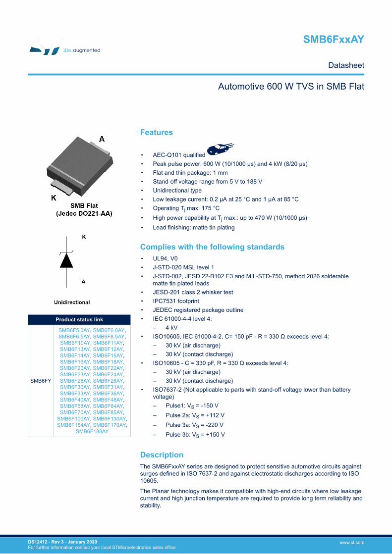
Features • AEC-Q101 qualified • Peak pulse power: 600 W (10/1000 μs) and 4 kW (8/20 μs) • Flat and thin package: 1 mm • Stand-off voltage range from 5 V to 188 V • Unidirectional type • Low leakage current: 0.2 μA at 25 °C and 1 μA at 85 °C • Operating T j max: 175 °C • High power capability at T j max.: up to 470 W (10/1000 µs) • Lead finishing: matte tin plating Complies with the following standards • UL94, V0 • J-STD-020 MSL level 1 • J-STD-002, JESD 22-B102 E3 and MIL-STD-750, method 2026 solderable matte tin plated leads • JESD-201 class 2 whisker test • IPC7531 footprint • JEDEC registered package outline • IEC 61000-4-4 level 4: – 4 kV • ISO10605, IEC 61000-4-2, C= 150 pF - R = 330 Ω exceeds level 4: – 30 kV (air discharge) – 30 kV (contact discharge) • ISO10605 - C = 330 pF, R = 330 Ω exceeds level 4: – 30 kV (air discharge) – 30 kV (contact discharge) • ISO7637-2 (Not applicable to parts with stand-off voltage lower than battery voltage) – Pulse1: V S = -150 V – Pulse 2a: V S = +112 V – Pulse 3a: V S = -220 V – Pulse 3b: V S = +150 V Description The SMB6FxxAY series are designed to protect sensitive automotive circuits against surges defined in ISO 7637-2 and against electrostatic discharges according to ISO 10605. The Planar technology makes it compatible with high-end circuits where low leakage current and high junction temperature are required to provide long term reliability and stability. Product status link SMB6FY SMB6F5.0AY, SMB6F6.0AY, SMB6F6.5AY, SMB6F8.5AY, SMB6F10AY, SMB6F11AY, SMB6F13AY, SMB6F12AY, SMB6F14AY, SMB6F15AY, SMB6F16AY, SMB6F18AY, SMB6F20AY, SMB6F22AY, SMB6F23AY, SMB6F24AY, SMB6F26AY, SMB6F28AY, SMB6F30AY, SMB6F31AY, SMB6F33AY, SMB6F36AY, SMB6F40AY, SMB6F48AY, SMB6F58AY, SMB6F64AY, SMB6F70AY, SMB6F85AY, SMB6F100AY, SMB6F130AY, SMB6F154AY, SMB6F170AY, SMB6F188AY Automotive 600 W TVS in SMB Flat SMB6FxxAY Datasheet DS12412 - Rev 3 - January 2020 For further information contact your local STMicroelectronics sales office. www.st.com
Transcript of SMB6FxxAY • IPC7531 footprint · smb6f85ay 0.2 1 85 95 100 105 1 137 4.6 7.17 178 22.5 3.29 10.6...
Features
• AEC-Q101 qualified• Peak pulse power: 600 W (10/1000 μs) and 4 kW (8/20 μs)• Flat and thin package: 1 mm• Stand-off voltage range from 5 V to 188 V• Unidirectional type• Low leakage current: 0.2 μA at 25 °C and 1 μA at 85 °C• Operating Tj max: 175 °C• High power capability at Tj max.: up to 470 W (10/1000 µs)• Lead finishing: matte tin plating
Complies with the following standards• UL94, V0• J-STD-020 MSL level 1• J-STD-002, JESD 22-B102 E3 and MIL-STD-750, method 2026 solderable
matte tin plated leads• JESD-201 class 2 whisker test• IPC7531 footprint• JEDEC registered package outline• IEC 61000-4-4 level 4:
– 4 kV• ISO10605, IEC 61000-4-2, C= 150 pF - R = 330 Ω exceeds level 4:
– 30 kV (air discharge)– 30 kV (contact discharge)
• ISO10605 - C = 330 pF, R = 330 Ω exceeds level 4:– 30 kV (air discharge)– 30 kV (contact discharge)
• ISO7637-2 (Not applicable to parts with stand-off voltage lower than batteryvoltage)– Pulse1: VS = -150 V– Pulse 2a: VS = +112 V– Pulse 3a: VS = -220 V– Pulse 3b: VS = +150 V
DescriptionThe SMB6FxxAY series are designed to protect sensitive automotive circuits againstsurges defined in ISO 7637-2 and against electrostatic discharges according to ISO10605.
The Planar technology makes it compatible with high-end circuits where low leakagecurrent and high junction temperature are required to provide long term reliability andstability.
Product status link
SMB6FY
SMB6F5.0AY, SMB6F6.0AY,SMB6F6.5AY, SMB6F8.5AY,SMB6F10AY, SMB6F11AY,SMB6F13AY, SMB6F12AY,SMB6F14AY, SMB6F15AY,SMB6F16AY, SMB6F18AY,SMB6F20AY, SMB6F22AY,SMB6F23AY, SMB6F24AY,SMB6F26AY, SMB6F28AY,SMB6F30AY, SMB6F31AY,SMB6F33AY, SMB6F36AY,SMB6F40AY, SMB6F48AY,SMB6F58AY, SMB6F64AY,SMB6F70AY, SMB6F85AY,
SMB6F100AY, SMB6F130AY,SMB6F154AY, SMB6F170AY,
SMB6F188AY
Automotive 600 W TVS in SMB Flat
SMB6FxxAY
Datasheet
DS12412 - Rev 3 - January 2020For further information contact your local STMicroelectronics sales office.
www.st.com
1 Characteristics
Table 1. Absolute maximum ratings (Tamb = 25 °C)
Symbol Parameter Value Unit
VPP Peak pulse voltage
ISO10605 (C = 330 pF, R = 330 Ω):
Contact discharge
Air discharge
30
30kV
ISO10605 / IEC 61000-4-2 (C = 150 pF, R = 330 Ω)
Contact discharge
Air discharge
30
30
PPP Peak pulse power dissipation 10/1000 µs, Tj initial = Tamb 600 W
Tstg Storage temperature range -65 to +175 °C
Tj Operating junction temperature range -55 to +175 °C
TL Maximum lead temperature for soldering during 10 s 260 °C
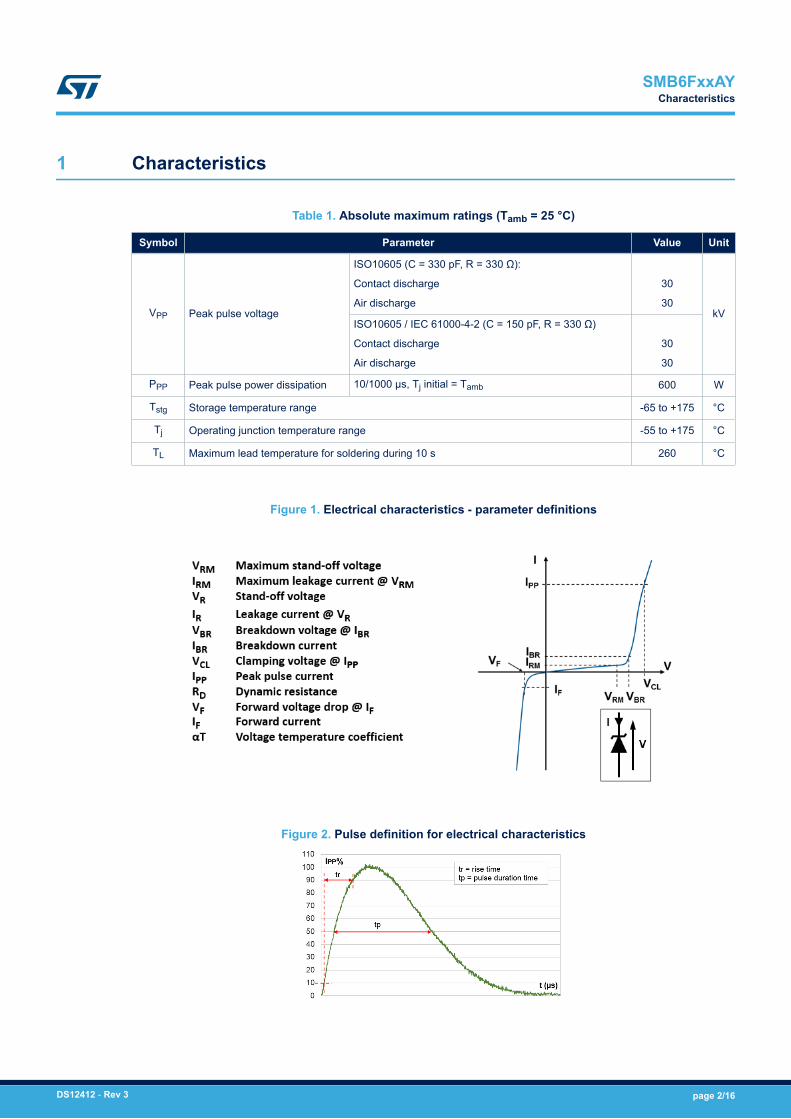
Figure 1. Electrical characteristics - parameter definitions
Figure 2. Pulse definition for electrical characteristics
SMB6FxxAYCharacteristics
DS12412 - Rev 3 page 2/16
Table 2. Electrical characteristics - parameter values (Tamb = 25 °C, unless otherwise specified)
Type
IRM max at VRM VBR at IBR (1)10 / 1000 µs 8 / 20µs
αTVCL(2)(3) IPP(4) RD VCL(2)(3) IPP(4) RD
25 °C 85 °C Min. Typ. Max. Max. Max. Max. Max. Max.
µA V V mA V A Ω V A Ω 10-4/°C
SMB6F5.0AY 20 50 5.0 6.4 6.74 7.1 10 9.2 68 0.031 13.4 298 0.021 5.7
SMB6F6.0AY 20 50 6.0 6.7 7.05 7.4 10 10.3 61 0.048 13.7 290 0.022 5.9
SMB6F6.5AY 20 50 6.5 7.2 7.58 8 10 11.2 56 0.057 14.5 276 0.024 6.1
SMB6F8.5AY 20 50 8.5 9.4 9.9 10.4 1 14.4 41.7 0.096 19.5 205 0.044 7.3
SMB6F10AY 0.2 1 10 11.1 11.7 12.3 1 17 37 0.127 21.7 184 0.051 7.8
SMB6F11AY 0.2 1 11 12.3 13 13.7 1 18 33.8 0.127 24.2 1665 0.064 8.1
SMB6F12AY 0.2 1 12 13.3 14 14.7 1 19.9 31 0.168 25.3 157 0.068 8.3
SMB6F13AY 0.2 1 13 14.4 15.2 16 1 21.5 29 0.190 27.2 147 0.076 8.4
SMB6F14AY 0.2 1 14 15.7 16.5 17.3 1 23.1 26 0.223 29 136 0.086 8.6
SMB6F15AY 0.2 1 15 16.7 17.6 18.5 1 24.4 25.1 0.235 32.5 123 0.114 8.8
SMB6F16AY 0.2 1 16 17.9 18.8 19.8 1 26 23.1 0.268 34.7 115 0.130 9.0
SMB6F18AY 0.2 1 18 20 21.1 22.2 1 29.2 21.5 0.326 39.3 102 0.168 9.2
SMB6F20AY 0.2 1 20 22.2 23.4 24.6 1 32.4 19.4 0.402 42.8 93 0.196 9.4
SMB6F22AY 0.2 1 22 24.4 25.7 27 1 35.5 17.7 0.480 48.3 83 0.257 9.6
SMB6F23AY 0.2 1 23 25.7 27 28.4 1 37.8 16.4 0.573 49.2 81 0.257 9.6
SMB6F24AY 0.2 1 24 26.7 28.1 29.5 1 38.9 16 0.588 50 80 0.256 9.6
SMB6F26AY 0.2 1 26 28.9 30.4 31.9 1 42.1 14.9 0.685 53.5 75 0.288 9.7
SMB6F28AY 0.2 1 28 31.1 32.7 34.3 1 45.4 13.8 0.804 59 68 0.363 9.8
SMB6F30AY 0.2 1 30 33.2 35 36.8 1 48.4 13 0.885 64.3 62 0.442 9.9
SMB6F31AY 0.2 1 31 34.2 36 37.8 1 50.2 12.3 1.01 65 61 0.45 9.9
SMB6F33AY 0.2 1 33 36.7 38.6 40.5 1 53.3 11.8 1.08 69.7 57 0.512 10
SMB6F36AY 0.2 1 36 40 42.1 44.2 1 58.1 10.3 1.35 76 52 0.612 10
SMB6F40AY 0.2 1 40 44.4 46.7 49 1 64.5 9.7 1.60 84 48 0.729 10.1
SMB6F48AY 0.2 1 48 53.2 56 58.8 1 77.4 8.1 2.28 100 40 1.03 10.3
SMB6F58AY 0.2 1 58 64.6 68 71.4 1 93.6 6.7 3.34 121 33 1.51 10.4
SMB6F64AY 0.2 1 64 71.1 74.8 78.6 1 103 5.8 4.17 134 30 1.84 10.5
SMB6F70AY 0.2 1 70 77.9 82 86.1 1 113 5.5 4.91 146 27 2.22 10.5
SMB6F85AY 0.2 1 85 95 100 105 1 137 4.6 7.17 178 22.5 3.29 10.6
SMB6F100AY 0.2 1 100 111 117 123 1 162 3.8 10.3 212 19 4.68 10.7
SMB6F130AY 0.2 1 130 144 152 160 1 209 3 16.3 265 15 7 10.8
SMB6F154AY 0.2 1 154 171 180 189 1 246 2.4 23.8 317 12.6 10.2 10.8
SMB6F170AY 0.2 1 170 190 200 210 1 275 2.2 30 353 11.3 12.7 10.8
SMB6F188AY 0.2 1 188 209 220 231 1 328 2 48.5 388 10.3 15.2 10.8
1. To calculate VBR versus Tj : VBR at Tj = VBR at 25 °C x (1 + αT x (Tj - 25))
2. To calculate VCL versus Tj : VCL at Tj = VCL at 25 °C x (1 + αT x (Tj - 25))
3. To calculate VCL max versus IPPappli: VCLmax = VBR max + RD x IPPappli
SMB6FxxAYCharacteristics
DS12412 - Rev 3 page 3/16
4. Surge capability given for both directions
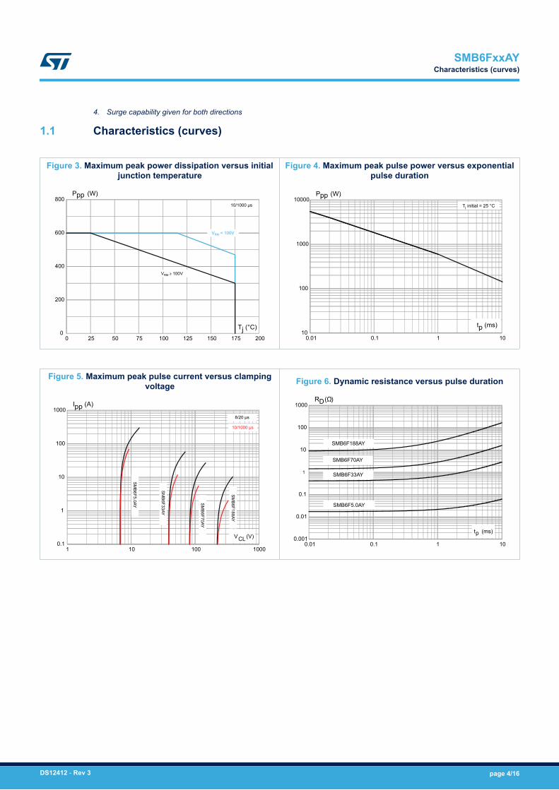
1.1 Characteristics (curves)
Figure 3. Maximum peak power dissipation versus initialjunction temperature
0
200
400
600
800
0 25 50 75 100 125 150 175 200
Ppp (W)
Tj (°C)
VRM < 100V
VRM ≥ 100V
10/1000 µs
Figure 4. Maximum peak pulse power versus exponentialpulse duration
10
100
1000
10000
0.01 0.1 1 10
Ppp (W)
tp (ms)
Tj initial = 25 °C
Figure 5. Maximum peak pulse current versus clampingvoltage
0.1
1
10
100
1000
1 10 100 1000
Ipp (A)
VCL (V)
SMB6F5.0AY
SMB6F33AY
SMB6F70AY
SMB6F188AY
8/20 µs
10/1000 µs
Figure 6. Dynamic resistance versus pulse duration
0.001
0.01
0.1
1
10
100
1000
0.01 0.1 1 10
RD(Ω)
tp (ms)
SMB6F5.0AY
SMB6F33AY
SMB6F70AY
SMB6F188AY
SMB6FxxAYCharacteristics (curves)
DS12412 - Rev 3 page 4/16
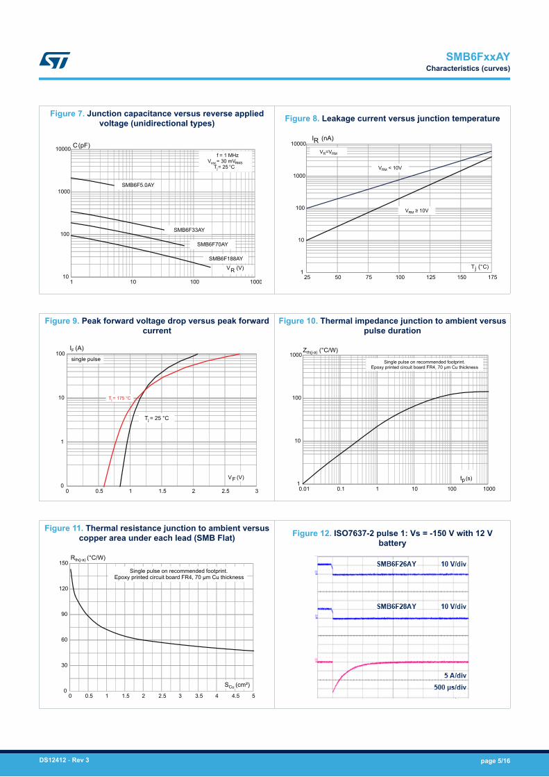
Figure 7. Junction capacitance versus reverse appliedvoltage (unidirectional types)
10
100
1000
10000
1 10 100 1000
C(pF)
VR (V)
SMB6F5.0AY
SMB6F33AY
SMB6F70AY
SMB6F188AY
f = 1 MHzVosc = 30 mVRMS
Tj = 25 °C
Figure 8. Leakage current versus junction temperature
1
10
100
1000
10000
25 50 75 100 125 150 175
IR (nA)
Tj (°C)
VR=VRM
VRM < 10V
VRM ≥ 10V
Figure 9. Peak forward voltage drop versus peak forwardcurrent
0
1
10
100
0 0.5 1 1.5 2 2.5 3
IF (A)
VF (V)
single pulseTj = 175 °C Tj = 25 °C
single pulse
Tj = 175 °C
Figure 10. Thermal impedance junction to ambient versuspulse duration
1
10
100
1000
0.01 0.1 1 10 100 1000
Zth(j-a) (°C/W)
tp (s)
Single pulse on recommended footprint.Epoxy printed circuit board FR4, 70 µm Cu thickness
Figure 11. Thermal resistance junction to ambient versuscopper area under each lead (SMB Flat)
0
30
60
90
120
150
0 0.5 1 1.5 2 2.5 3 3.5 4 4.5 5
Rth(j-a) (°C/W)
SCu (cm²)
Single pulse on recommended footprint.Epoxy printed circuit board FR4, 70 µm Cu thickness
Figure 12. ISO7637-2 pulse 1: Vs = -150 V with 12 Vbattery
SMB6FxxAYCharacteristics (curves)
DS12412 - Rev 3 page 5/16
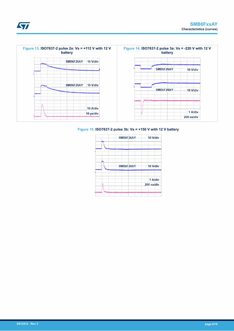
Figure 13. ISO7637-2 pulse 2a: Vs = +112 V with 12 Vbattery
Figure 14. ISO7637-2 pulse 3a: Vs = -220 V with 12 Vbattery
Figure 15. ISO7637-2 pulse 3b: Vs = +150 V with 12 V battery
SMB6FxxAYCharacteristics (curves)
DS12412 - Rev 3 page 6/16
2 Package information
In order to meet environmental requirements, ST offers these devices in different grades of ECOPACK packages,depending on their level of environmental compliance. ECOPACK specifications, grade definitions and productstatus are available at: www.st.com. ECOPACK is an ST trademark.
SMB6FxxAYPackage information
DS12412 - Rev 3 page 7/16
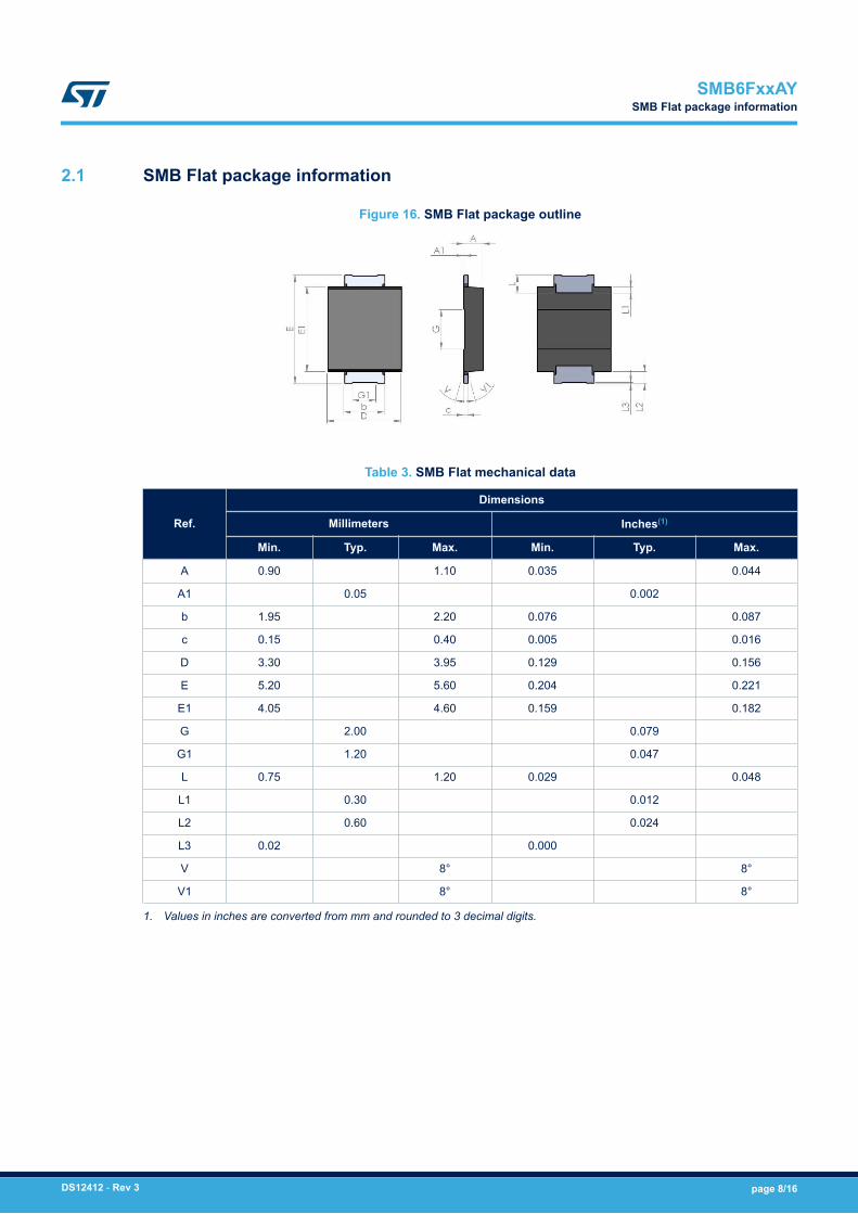
2.1 SMB Flat package information
Figure 16. SMB Flat package outline
Table 3. SMB Flat mechanical data
Ref.
Dimensions
Millimeters Inches(1)
Min. Typ. Max. Min. Typ. Max.
A 0.90 1.10 0.035 0.044
A1 0.05 0.002
b 1.95 2.20 0.076 0.087
c 0.15 0.40 0.005 0.016
D 3.30 3.95 0.129 0.156
E 5.20 5.60 0.204 0.221
E1 4.05 4.60 0.159 0.182
G 2.00 0.079
G1 1.20 0.047
L 0.75 1.20 0.029 0.048
L1 0.30 0.012
L2 0.60 0.024
L3 0.02 0.000
V 8° 8°
V1 8° 8°
1. Values in inches are converted from mm and rounded to 3 decimal digits.
SMB6FxxAYSMB Flat package information
DS12412 - Rev 3 page 8/16
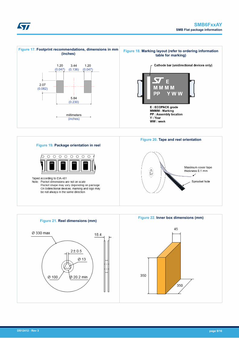
Figure 17. Footprint recommendations, dimensions in mm(inches)
5.84(0.230)
1.20(0.047)
3.44(0.136)
1.20(0.047)
2.07(0.082)
millimeters(inches)
Figure 18. Marking layout (refer to ordering informationtable for marking)
Figure 19. Package orientation in reelFigure 20. Tape and reel orientation
Figure 21. Reel dimensions (mm)Figure 22. Inner box dimensions (mm)
SMB6FxxAYSMB Flat package information
DS12412 - Rev 3 page 9/16
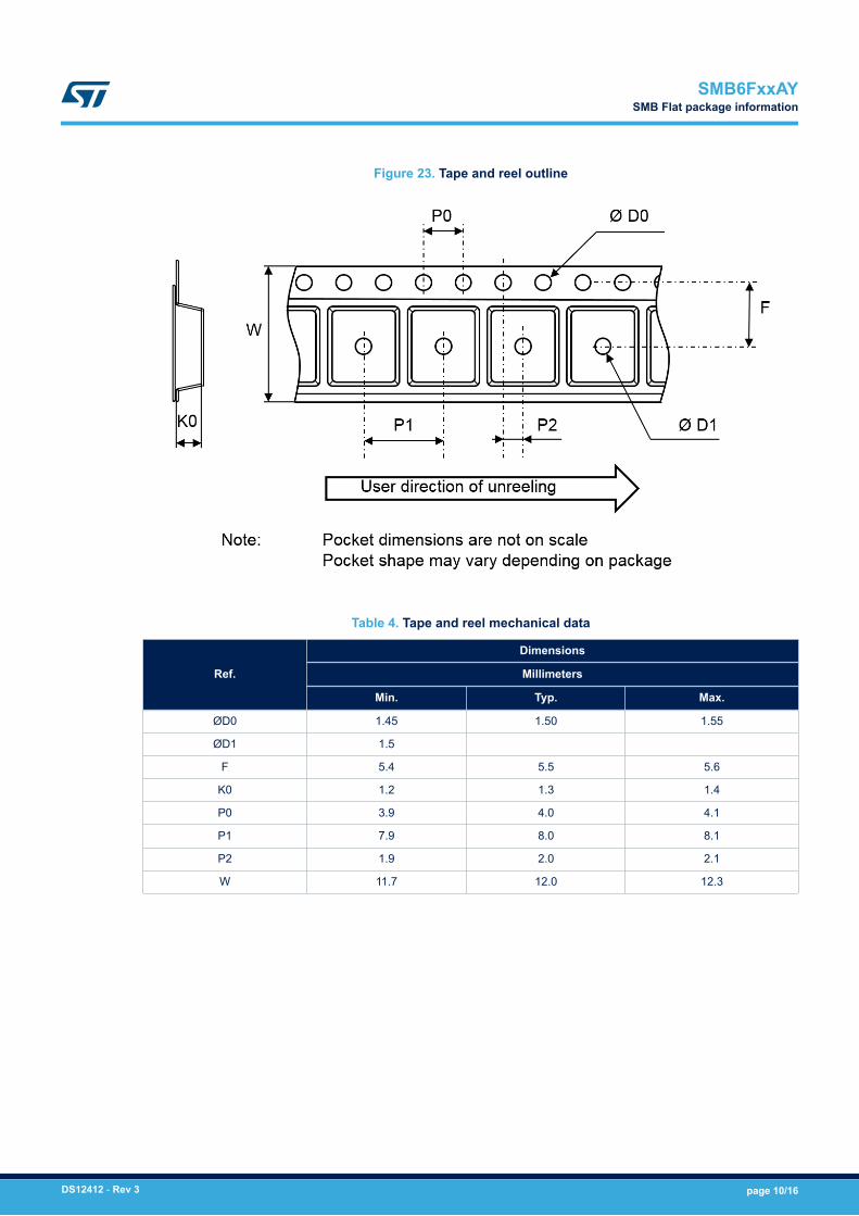
Figure 23. Tape and reel outline
Table 4. Tape and reel mechanical data
Ref.
Dimensions
Millimeters
Min. Typ. Max.
ØD0 1.45 1.50 1.55
ØD1 1.5
F 5.4 5.5 5.6
K0 1.2 1.3 1.4
P0 3.9 4.0 4.1
P1 7.9 8.0 8.1
P2 1.9 2.0 2.1
W 11.7 12.0 12.3
SMB6FxxAYSMB Flat package information
DS12412 - Rev 3 page 10/16
2.2 Reflow profile
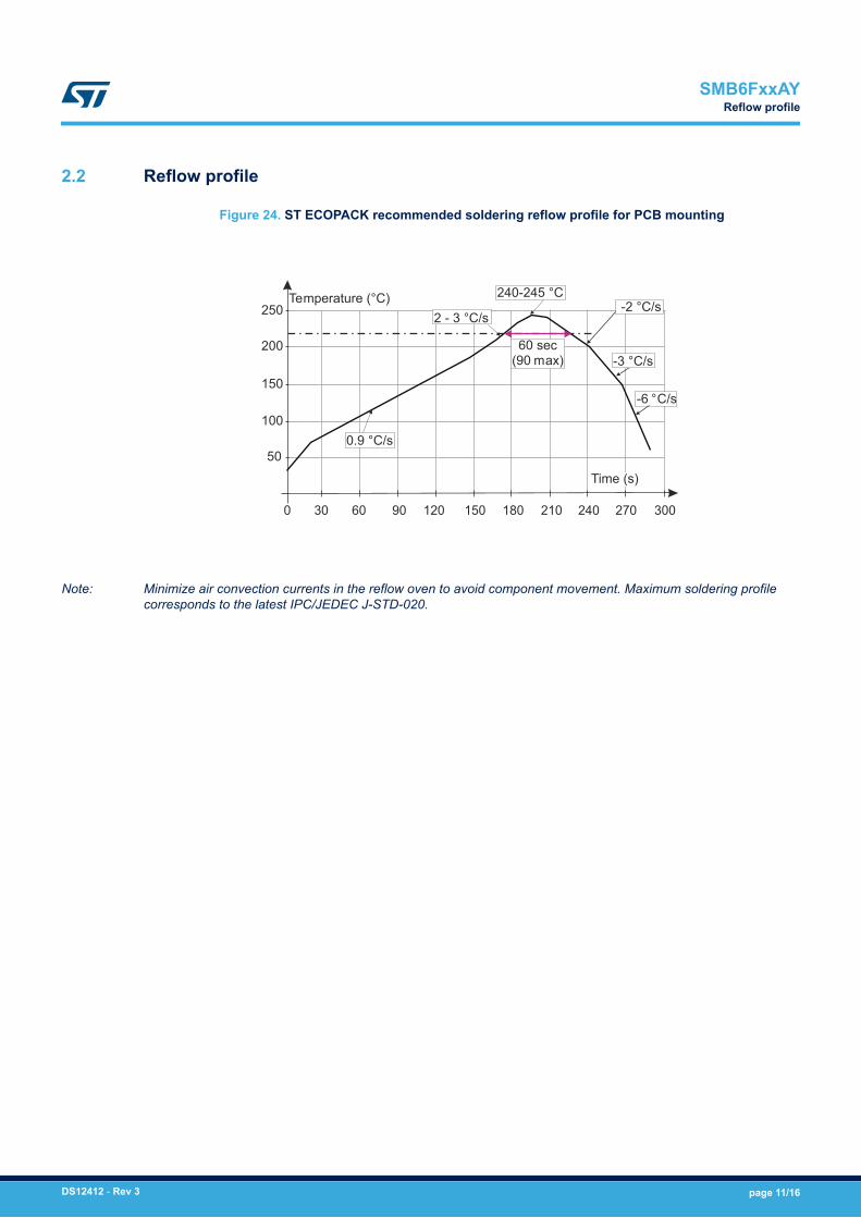
Figure 24. ST ECOPACK recommended soldering reflow profile for PCB mounting
250
0
50
100
150
200
240210180150120906030 300270
-6 °C/s
240-245 °C
2 - 3 °C/sTemperature (°C) -2 °C/s
-3 °C/s
Time (s)
0.9 °C/s
60 sec(90 max)
Note: Minimize air convection currents in the reflow oven to avoid component movement. Maximum soldering profilecorresponds to the latest IPC/JEDEC J-STD-020.
SMB6FxxAYReflow profile
DS12412 - Rev 3 page 11/16
3 Application and design guidelines
More information is available in the application note AN2689 “Protection of automotive electronics from electricalhazards, guidelines for design and component selection”.
SMB6FxxAYApplication and design guidelines
DS12412 - Rev 3 page 12/16
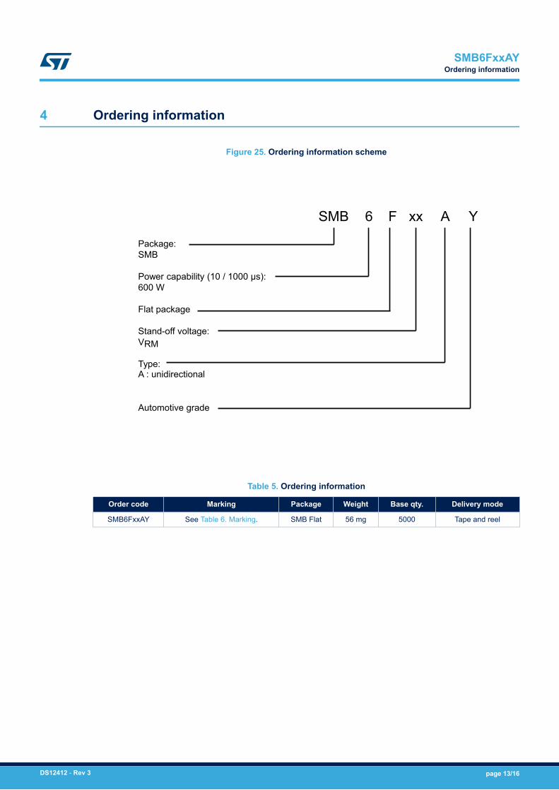
4 Ordering information
Figure 25. Ordering information scheme
SMB 6 F xx A Y
Package:SMB
Power capability (10 / 1000 µs):600 W
Flat package
Stand-off voltage:VRM
Type:A : unidirectional
Automotive grade
Table 5. Ordering information
Order code Marking Package Weight Base qty. Delivery mode
SMB6FxxAY See Table 6. Marking. SMB Flat 56 mg 5000 Tape and reel
SMB6FxxAYOrdering information
DS12412 - Rev 3 page 13/16
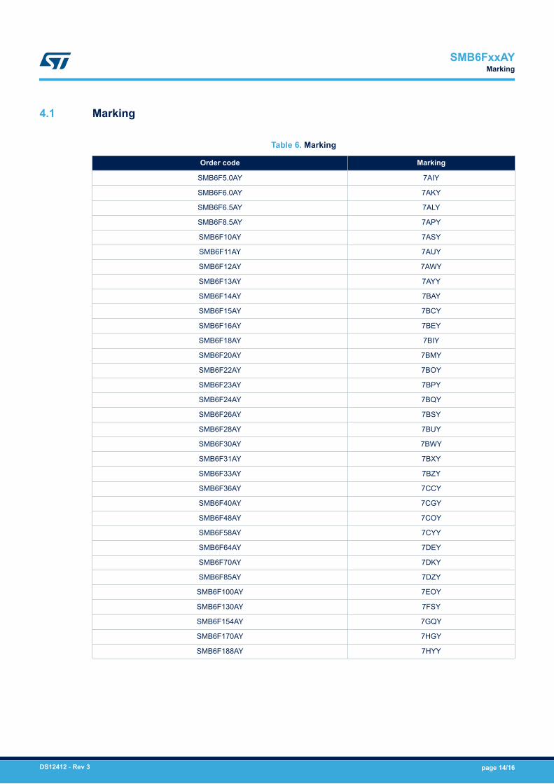
4.1 Marking
Table 6. Marking
Order code Marking
SMB6F5.0AY 7AIY
SMB6F6.0AY 7AKY
SMB6F6.5AY 7ALY
SMB6F8.5AY 7APY
SMB6F10AY 7ASY
SMB6F11AY 7AUY
SMB6F12AY 7AWY
SMB6F13AY 7AYY
SMB6F14AY 7BAY
SMB6F15AY 7BCY
SMB6F16AY 7BEY
SMB6F18AY 7BIY
SMB6F20AY 7BMY
SMB6F22AY 7BOY
SMB6F23AY 7BPY
SMB6F24AY 7BQY
SMB6F26AY 7BSY
SMB6F28AY 7BUY
SMB6F30AY 7BWY
SMB6F31AY 7BXY
SMB6F33AY 7BZY
SMB6F36AY 7CCY
SMB6F40AY 7CGY
SMB6F48AY 7COY
SMB6F58AY 7CYY
SMB6F64AY 7DEY
SMB6F70AY 7DKY
SMB6F85AY 7DZY
SMB6F100AY 7EOY
SMB6F130AY 7FSY
SMB6F154AY 7GQY
SMB6F170AY 7HGY
SMB6F188AY 7HYY
SMB6FxxAYMarking
DS12412 - Rev 3 page 14/16
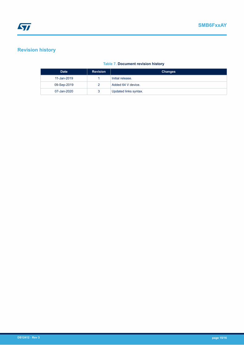
Revision history
Table 7. Document revision history
Date Revision Changes
11-Jan-2019 1 Initial release.
09-Sep-2019 2 Added 64 V device.
07-Jan-2020 3 Updated links syntax.
SMB6FxxAY
DS12412 - Rev 3 page 15/16
IMPORTANT NOTICE – PLEASE READ CAREFULLY
STMicroelectronics NV and its subsidiaries (“ST”) reserve the right to make changes, corrections, enhancements, modifications, and improvements to STproducts and/or to this document at any time without notice. Purchasers should obtain the latest relevant information on ST products before placing orders. STproducts are sold pursuant to ST’s terms and conditions of sale in place at the time of order acknowledgement.
Purchasers are solely responsible for the choice, selection, and use of ST products and ST assumes no liability for application assistance or the design ofPurchasers’ products.
No license, express or implied, to any intellectual property right is granted by ST herein.
Resale of ST products with provisions different from the information set forth herein shall void any warranty granted by ST for such product.
ST and the ST logo are trademarks of ST. For additional information about ST trademarks, please refer to www.st.com/trademarks. All other product or servicenames are the property of their respective owners.
Information in this document supersedes and replaces information previously supplied in any prior versions of this document.
© 2020 STMicroelectronics – All rights reserved
SMB6FxxAY
DS12412 - Rev 3 page 16/16

![Research Paper Combination Therapy of TGF-β Blockade and … · 2019-05-29 · (0.2 g/L), and metronidazole (0.2 g/L) in their drinking water for 1 week [24]. Fresh drinking water](https://static.fdocument.org/doc/165x107/5f801928f00b6a5fb7561c05/research-paper-combination-therapy-of-tgf-blockade-and-2019-05-29-02-gl.jpg)