
Silicon Photonics at Intel 50Gbps Integrated Link - Hot Chips · 4λx10Gbps SiP Tx & Rx Packages...
29
1 1 Demonstration of a High Speed 4-Channel Integrated Silicon Photonics WDM Link with Hybrid Silicon Lasers Andrew Alduino Intel Corporation, 2200 Mission College Boulevard, Santa Clara CA 95054
Transcript of Silicon Photonics at Intel 50Gbps Integrated Link - Hot Chips · 4λx10Gbps SiP Tx & Rx Packages...
1 1
Demonstration of a High Speed 4-Channel Integrated Silicon Photonics WDM Link with Hybrid Silicon Lasers
Andrew Alduino
I ntel Corporat ion, 2200 Mission College Boulevard, Santa Clara CA
95054
22
Outline
• Introduction
• Previous Results
• WDM Silicon Photonics
Link
• Link Testing Results
• Summary
33
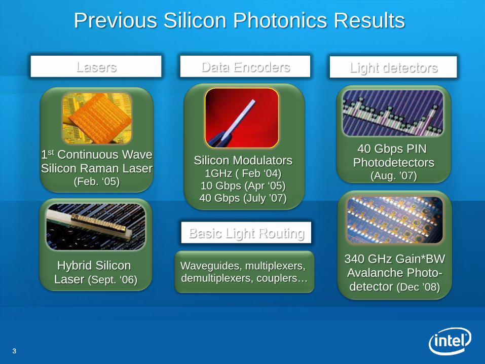
Previous Silicon Photonics Results
Lasers Data Encoders Light detectors
Hybrid Silicon Laser (Sept. ‘06)
40 Gbps PIN Photodetectors
(Aug. ’07)Silicon Modulators
1GHz ( Feb ‘04)10 Gbps (Apr ‘05)40 Gbps (July ’07)
340 GHz Gain*BWAvalanche Photo-detector (Dec ’08)
1st Continuous WaveSilicon Raman Laser
(Feb. ‘05)
Basic Light Routing
Waveguides, multiplexers, demultiplexers, couplers…
44
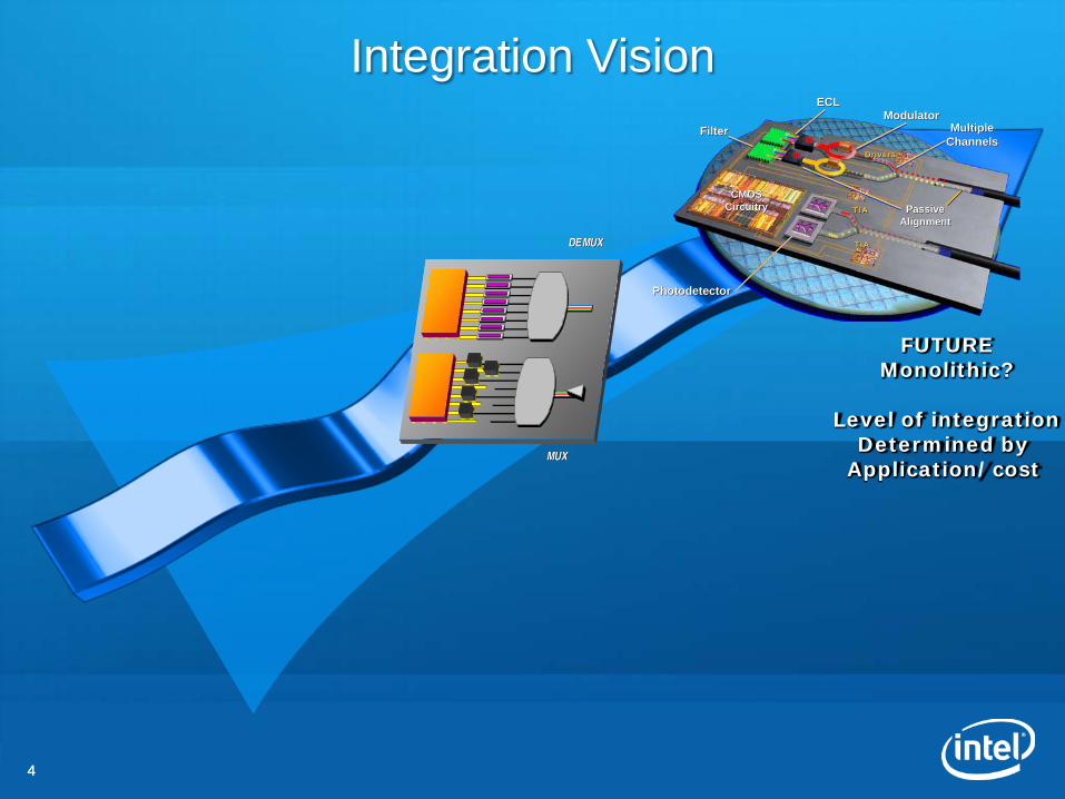
Integration Vision
TIATIA
TIATIA
DriversDrivers
TIATIA
TIATIA
DriversDrivers
CMOSCMOSCircuitryCircuitry
PhotodetectorPhotodetector
PassivePassiveAlignmentAlignment
ModulatorModulatorECLECL
FilterFilter MultipleMultipleChannelsChannels
FUTUREMonolithic?
Level of integrat ionDeterm ined by
Applicat ion/ cost
DEMUXDEMUX
MUXMUX

55
Outline
• Introduction
• Previous Results
• WDM Silicon Photonics
Link
• Link Testing Results
• Summary
66
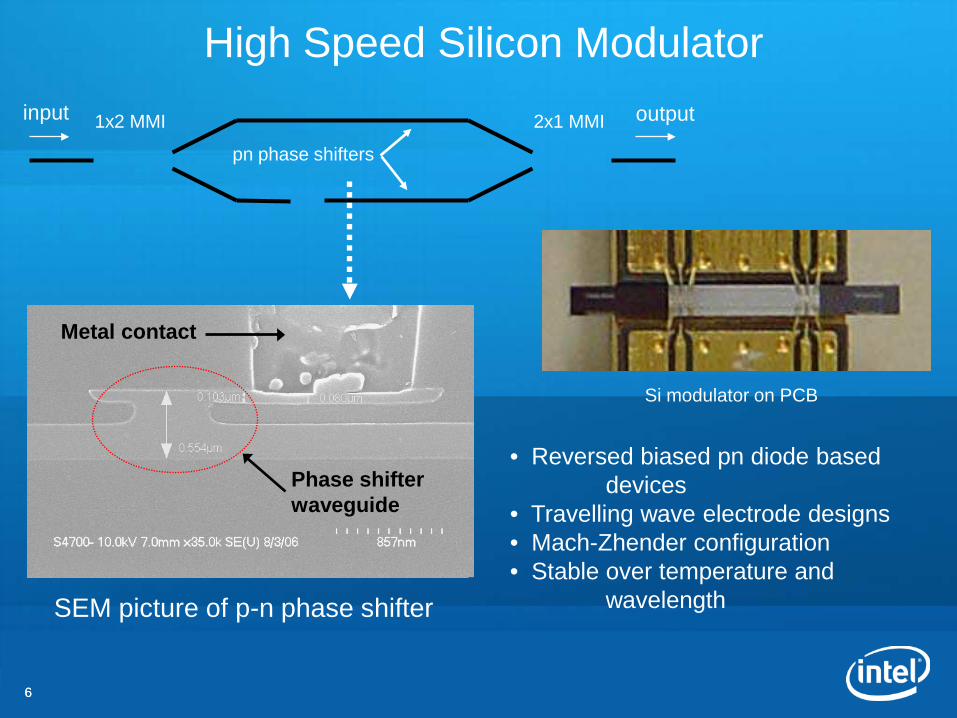
High Speed Silicon Modulator
Phase shifterwaveguide
Metal contact
SEM picture of p-n phase shifter
Si modulator on PCB
1x2 MMI 2x1 MMI
pn phase shifters
input output
• Reversed biased pn diode based devices
• Travelling wave electrode designs• Mach-Zhender configuration• Stable over temperature and
wavelength
77
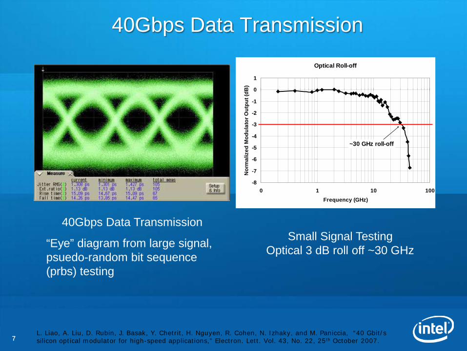
Optical Roll-off
-8
-7
-6
-5
-4
-3
-2
-1
0
1
0 1 10 100
Frequency (GHz)
No
rmal
ized
Mo
du
lato
r O
utp
ut (
dB
)
~30 GHz roll-off
40Gbps Data Transmission
Small Signal TestingOptical 3 dB roll off ~30 GHz
40Gbps Data Transmission
“Eye” diagram from large signal, psuedo-random bit sequence (prbs) testing
L. Liao, A. Liu, D. Rubin, J. Basak, Y. Chet rit , H. Nguyen, R. Cohen, N. I zhaky, and M. Paniccia, “40 Gbit / s silicon opt ical m odulator for high-speed applicat ions,” Elect ron. Let t . Vol. 43, No. 22, 25 th October 2007.
88
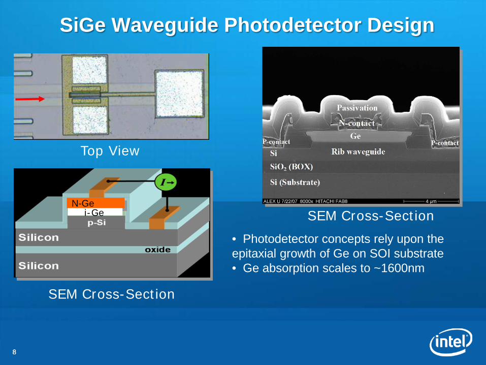
SiGe Waveguide Photodetector Design
SEM Cross-Sect ionN-Ge
i-Ge
Top View
SEM Cross-Sect ion
• Photodetector concepts rely upon the epitaxial growth of Ge on SOI substrate• Ge absorption scales to ~1600nm
99
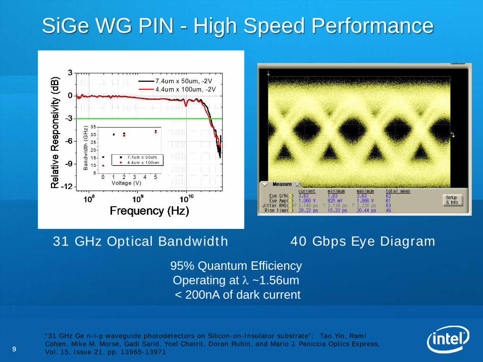
SiGe WG PIN - High Speed Performance
31 GHz Opt ical Bandwidth 40 Gbps Eye Diagram
95% Quantum EfficiencyOperating at λ ~1.56um< 200nA of dark current
“31 GHz Ge n- i-p waveguide photodetectors on Silicon-on- Insulator subst rate” ; Tao Yin, Ram i Cohen, Mike M. Morse, Gadi Sarid, Yoel Chet rit , Doron Rubin, and Mario J. Paniccia Opt ics Express, Vol. 15, I ssue 21, pp. 13965-13971
1010
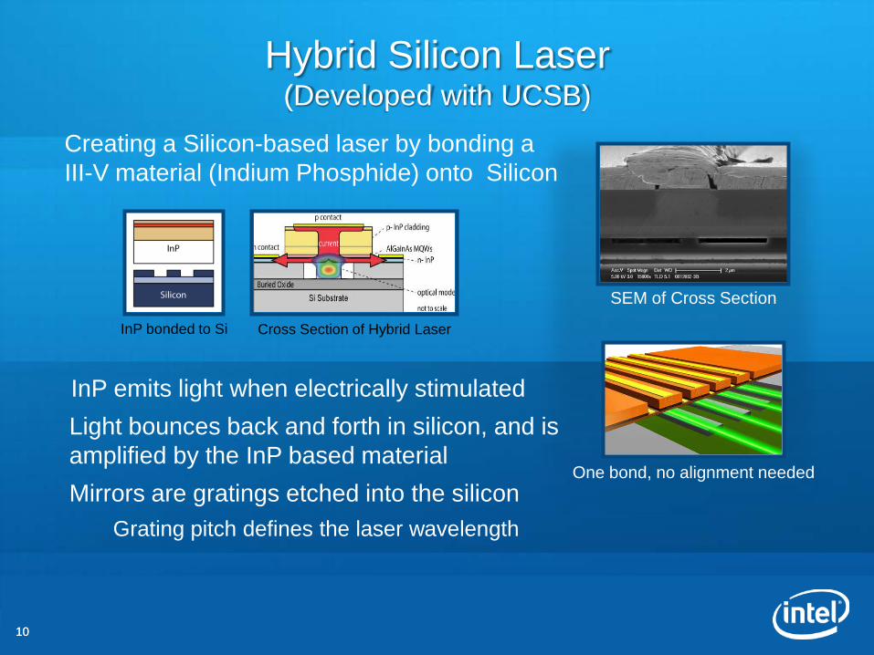
Creating a Silicon-based laser by bonding a III-V material (Indium Phosphide) onto Silicon
InP emits light when electrically stimulated
Light bounces back and forth in silicon, and is amplified by the InP based material
Mirrors are gratings etched into the siliconGrating pitch defines the laser wavelength
Hybrid Silicon Laser (Developed with UCSB)
InP bonded to Si Cross Section of Hybrid Laser
One bond, no alignment needed
SEM of Cross Section
1111
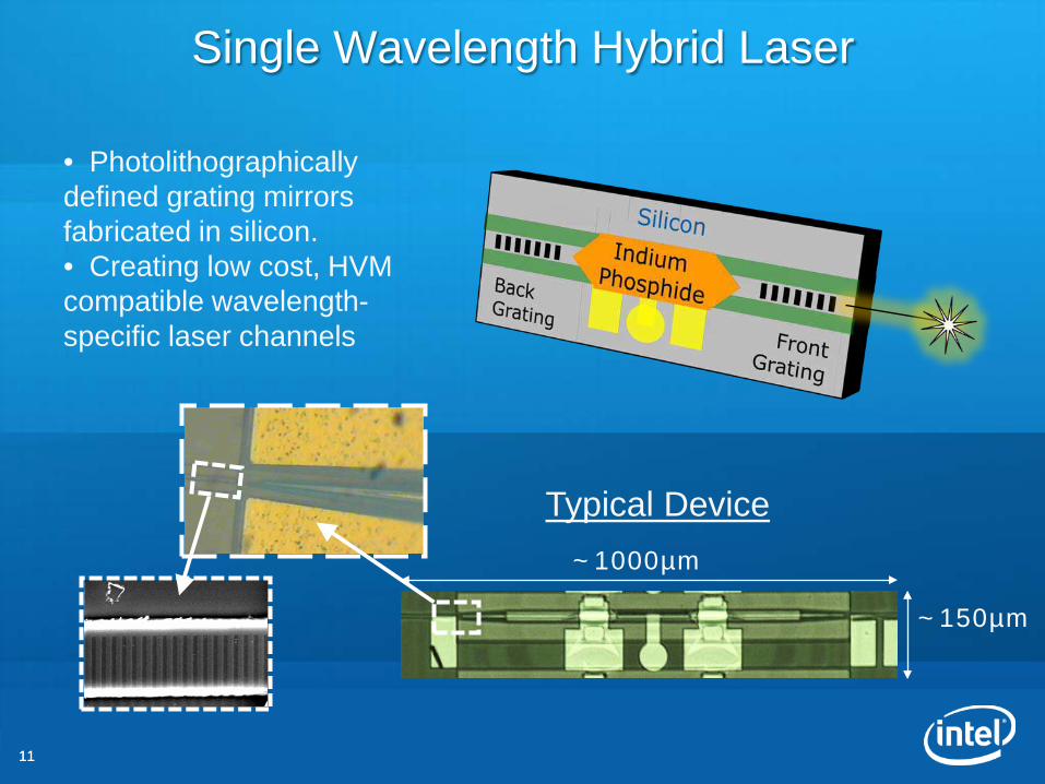
Single Wavelength Hybrid Laser
~ 150µm
~ 1000µm
Typical Device
• Photolithographicallydefined grating mirrors fabricated in silicon.• Creating low cost, HVM compatible wavelength-specific laser channels
1212
Outline
• Introduction
• Previous Results
• WDM Silicon Photonics
Link
• Link Testing Results
• Summary
1313
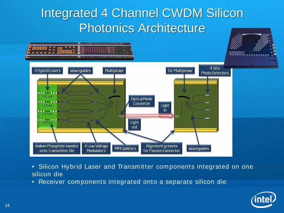
Integrated 4 Channel CWDM Silicon Photonics Architecture
• Silicon Hybrid Laser and Transm it ter components integrated on one silicon die• Receiver components integrated onto a separate silicon die
1414
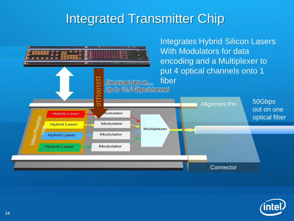
Integrated Transmitter Chip
1101001110
Electrical data in…Up to 12.5 Gbps/channel
50Gbps out on oneoptical fiber
Connector
Alignment Pin
Integrates Hybrid Silicon LasersWith Modulators for data encoding and a Multiplexer to put 4 optical channels onto 1 fiber
1515
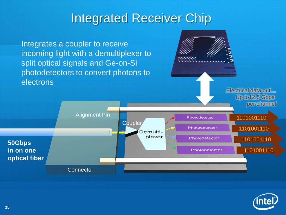
Integrated Receiver Chip
50Gbps in on oneoptical fiber
Connector
Alignment Pin
Coupler
Integrates a coupler to receive incoming light with a demultiplexer to split optical signals and Ge-on-Si photodetectors to convert photons to electrons
1101001110
1101001110
1101001110
1101001110
Electrical data out…Up to12.5 Gbps
per channel
1616
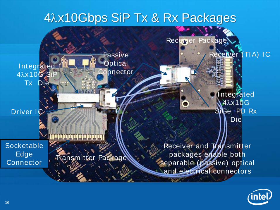
4λx10Gbps SiP Tx & Rx Packages
Transm it ter Package
Receiver Package
Driver I C
I ntegrated 4λx10G SiP
Tx Die
SocketableEdge
Connector
Receiver (TI A) I C
I ntegrated 4λx10G
SiGe PD Rx Die
Passive Opt ical
Connector
Receiver and Transm it ter packages enable both
separable (passive) opt ical and elect r ical connectors
1717
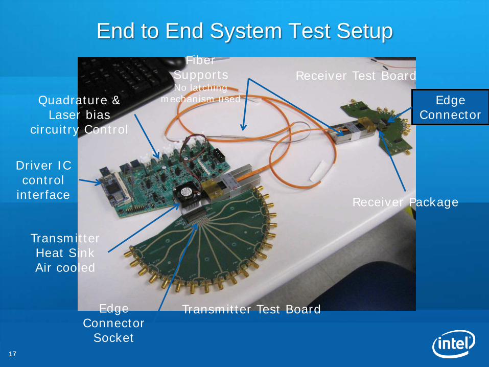
End to End System Test Setup
Transm it ter Test Board
Receiver Test Board
Transm it ter Heat SinkAir cooled
Driver I C cont rol
interface
Edge Connector
Socket
Receiver Package
Edge Connector
Fiber SupportsNo latching
m echanism usedQuadrature & Laser bias
circuit ry Cont rol
1818
Outline
• Introduction
• Previous Results
• WDM Silicon Photonics
Link
• Link Testing Results
• Summary
1919
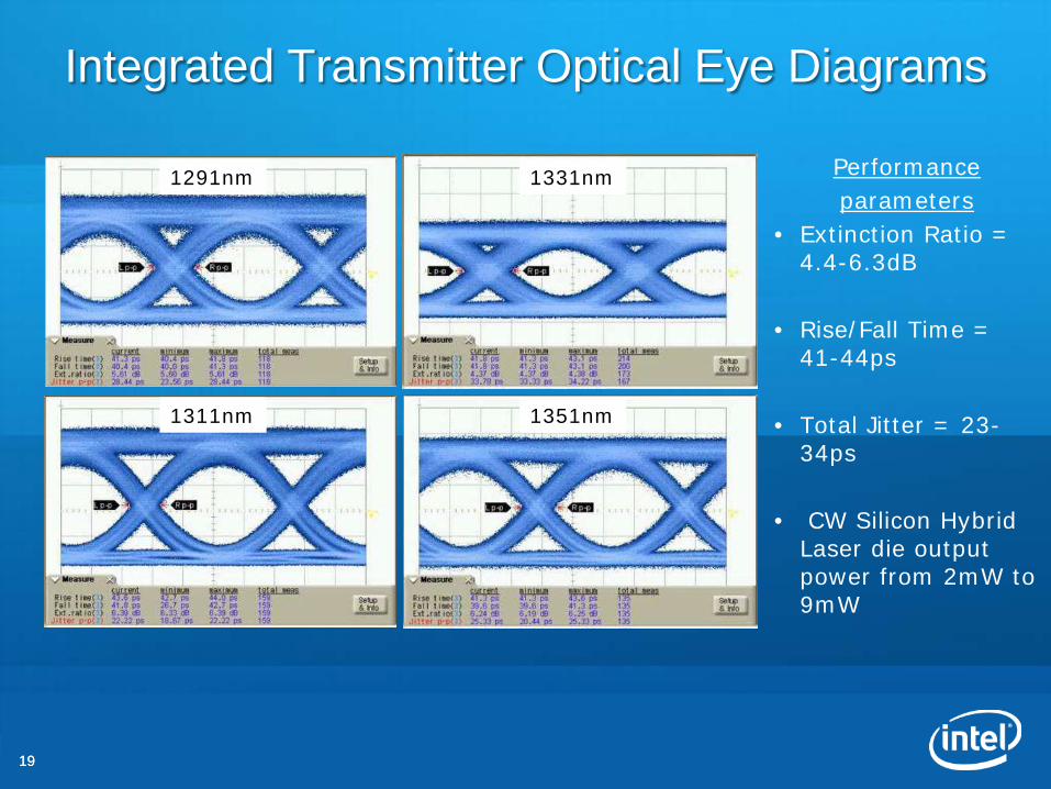
Integrated Transmitter Optical Eye Diagrams
Performanceparameters
• Ext inct ion Rat io = 4.4-6.3dB
• Rise/ Fall Time = 41-44ps
• Total Jit ter = 23-34ps
• CW Silicon Hybrid Laser die output power from 2mW to 9mW
1291nm
1311nm
1331nm
1351nm
2020
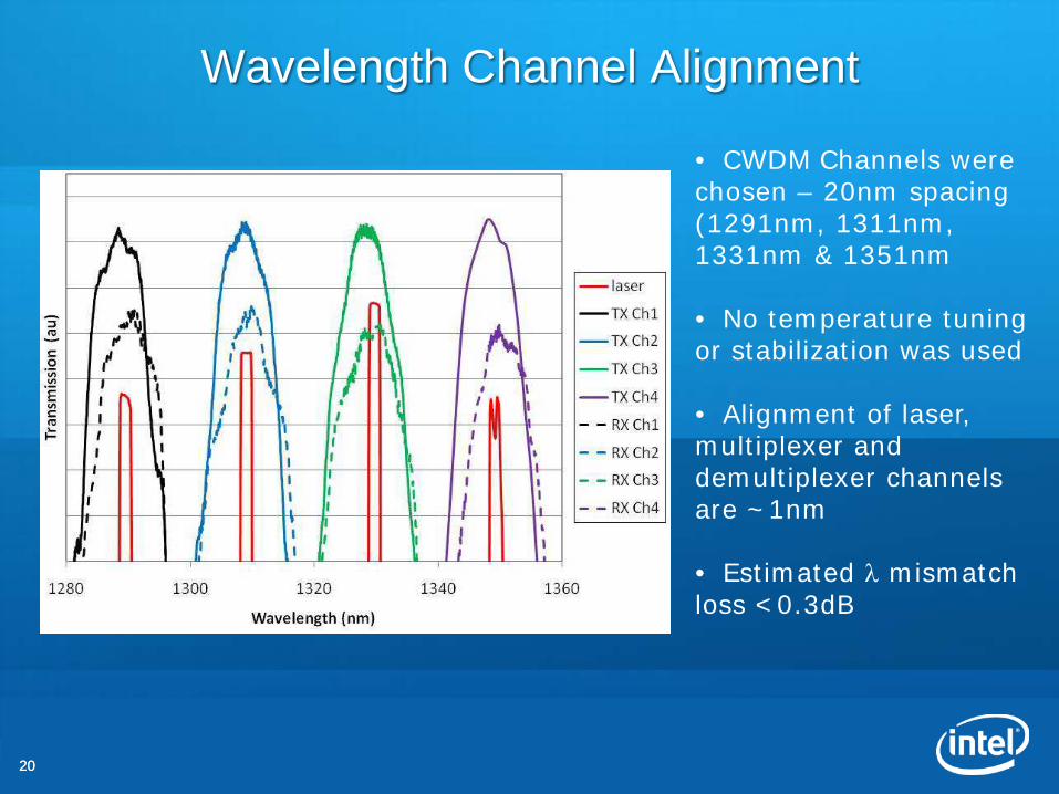
Wavelength Channel Alignment
• CWDM Channels were chosen – 20nm spacing (1291nm , 1311nm , 1331nm & 1351nm
• No tem perature tuning or stabilizat ion was used
• Alignm ent of laser, m ult iplexer and dem ult iplexer channels are ~ 1nm
• Est im ated λ m ism atch loss < 0.3dB
2121
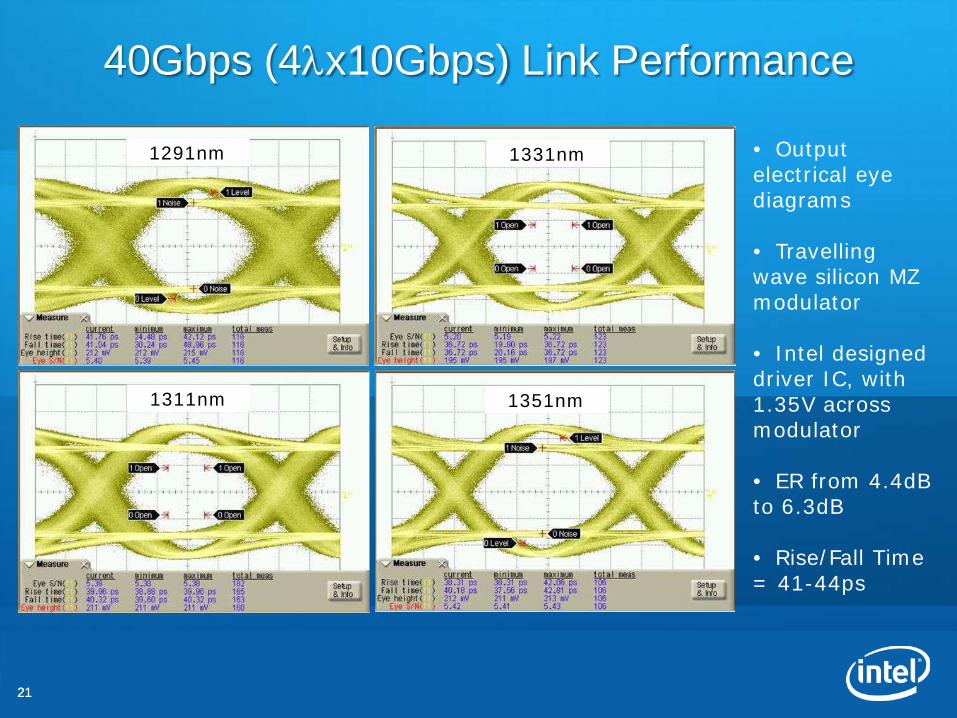
40Gbps (4λx10Gbps) Link Performance
• Output elect r ical eye diagrams
• Travelling wave silicon MZ modulator
• I ntel designed dr iver I C, with 1.35V across modulator
• ER from 4.4dB to 6.3dB
• Rise/ Fall Time = 41-44ps
1291nm
1311nm
1331nm
1351nm
2222
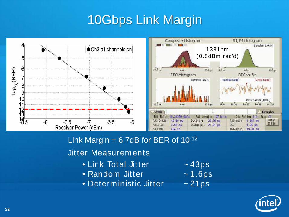
10Gbps Link Margin
Rx module optical loss = 7.8 dB
Link Margin = 6.7dB for BER of 10-12
Jit ter Measurements• Link Total Jit ter ~ 43ps • Random Jit ter ~ 1.6ps • Determ inist ic Jit ter ~ 21ps
1331nm(0.5dBm rec’d)
2323
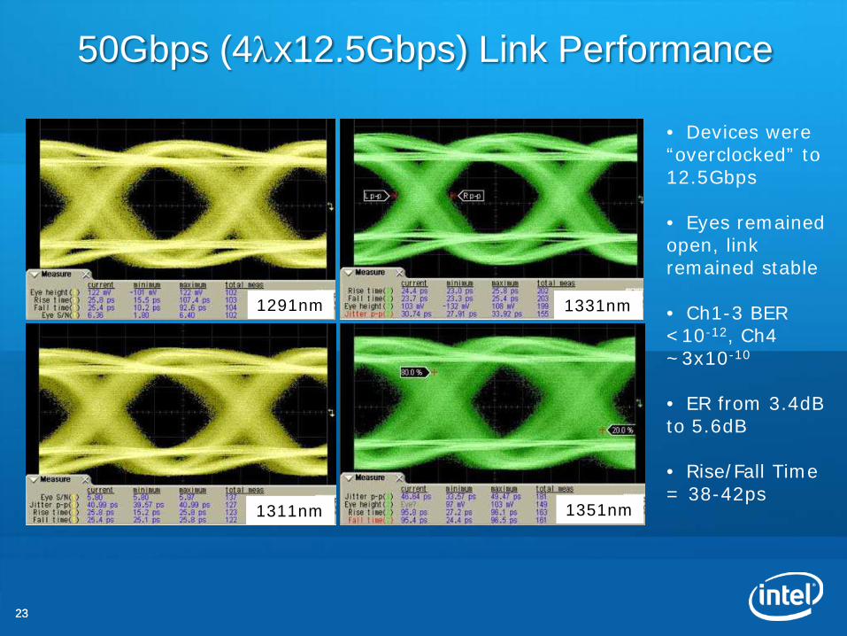
50Gbps (4λx12.5Gbps) Link Performance
1291nm
1311nm
1331nm
1351nm
• Devices were “overclocked” to 12.5Gbps
• Eyes remained open, link remained stable
• Ch1-3 BER < 10 -12, Ch4 ~ 3x10 -10
• ER from 3.4dB to 5.6dB
• Rise/ Fall Time = 38-42ps

2424
Outline
• Introduction
• Previous Results
• WDM Silicon Photonics
Link
• Link Testing Results
• Summary
2525
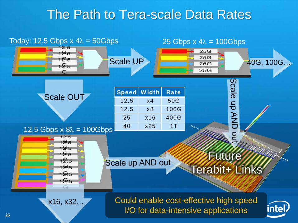
The Path to Tera-scale Data Rates
Scale UP 40G, 100G…
Scale OUT
x16, x32…
Future Terabit+ Links
Today: 12.5 Gbps x 4λ = 50Gbps
12.5 Gbps x 8λ = 100Gbps
25 Gbps x 4λ = 100Gbps
Speed W idth Rate12.5 x4 50G
12.5 x8 100G
25 x16 400G
40 x25 1T
Could enable cost-effective high speed I/O for data-intensive applications
2626
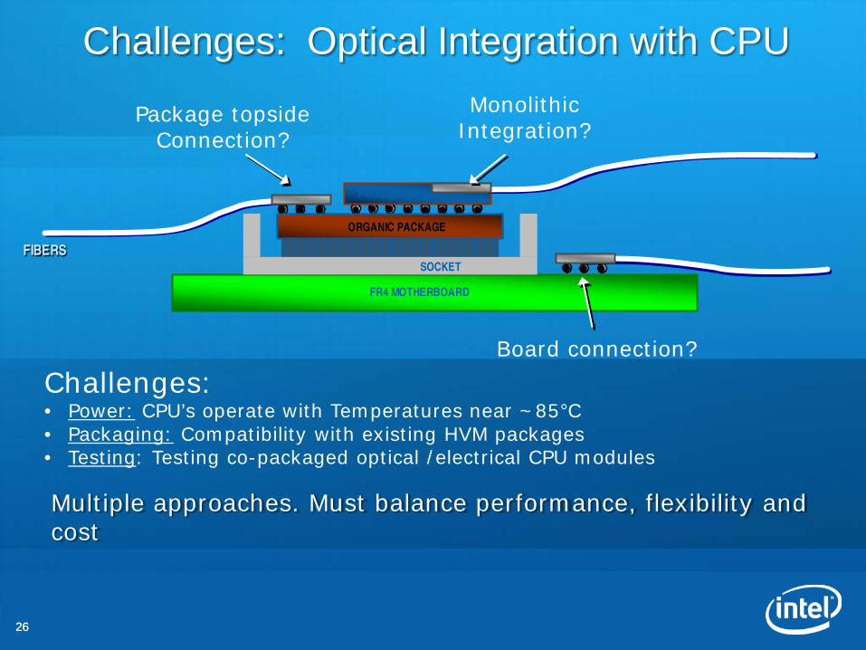
Challenges: Optical Integration with CPU
Package topsideConnect ion?
Board connect ion?
MonolithicI ntegrat ion?
PROCESSOR
ORGANIC PACKAGE
SOCKET
FR4 MOTHERBOARD
Mult iple approaches. Must balance performance, flexibility and cost
FIBERS
Challenges:• Power: CPU’s operate with Tem peratures near ~ 85°C• Packaging: Compat ibility with exist ing HVM packages• Test ing: Test ing co-packaged opt ical / elect r ical CPU modules
2727
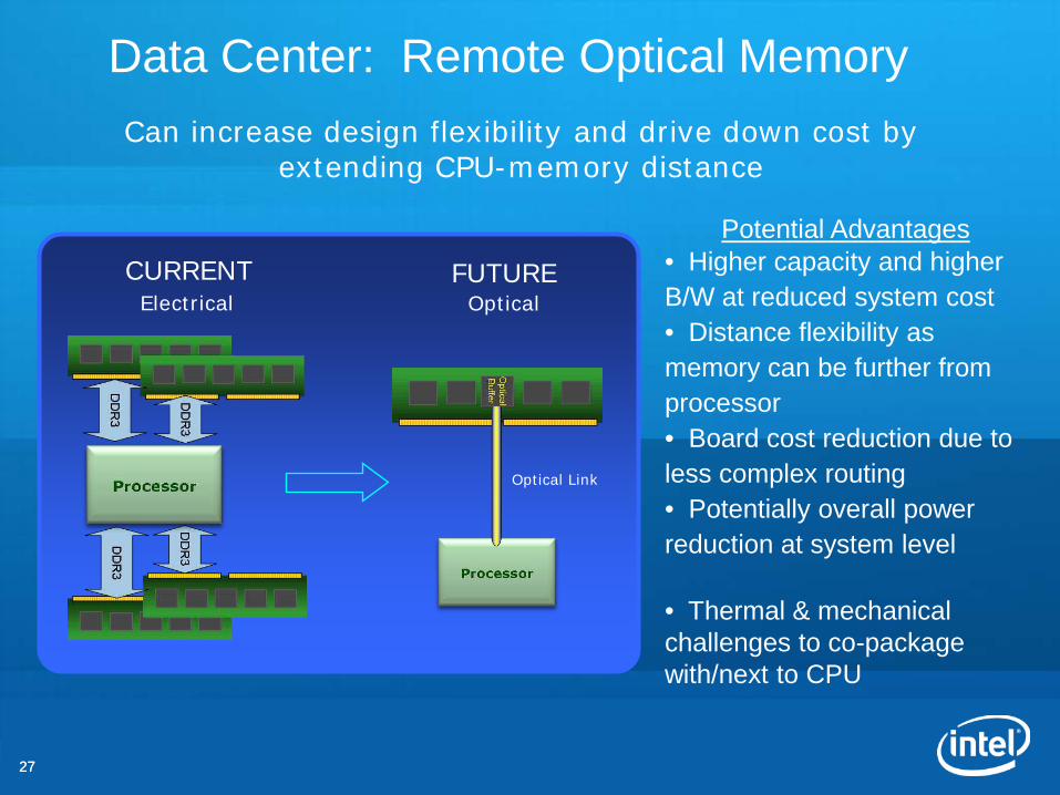
Data Center: Remote Optical Memory
CURRENT FUTURE
Opt ical Link
Opt icalElect r ical
Can increase design flexibility and drive down cost by extending CPU-memory distance
Potential Advantages• Higher capacity and higher B/W at reduced system cost • Distance flexibility as memory can be further from processor• Board cost reduction due to less complex routing• Potentially overall power reduction at system level
• Thermal & mechanical challenges to co-package with/next to CPU
2828
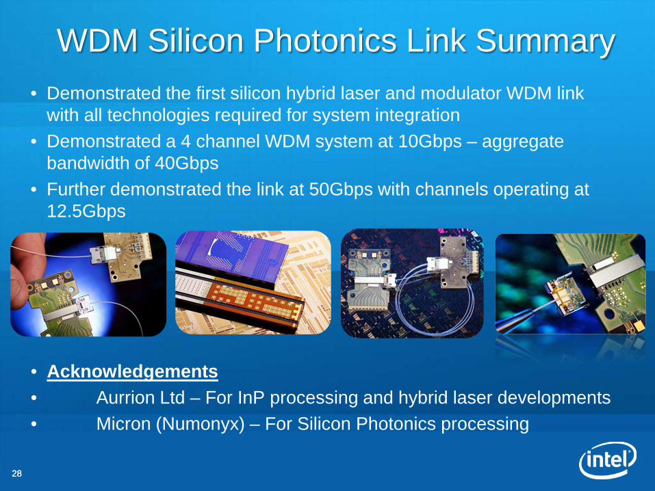
WDM Silicon Photonics Link Summary
• Demonstrated the first silicon hybrid laser and modulator WDM link with all technologies required for system integration
• Demonstrated a 4 channel WDM system at 10Gbps – aggregate bandwidth of 40Gbps
• Further demonstrated the link at 50Gbps with channels operating at 12.5Gbps
• Acknowledgements• Aurrion Ltd – For InP processing and hybrid laser developments• Micron (Numonyx) – For Silicon Photonics processing

29
Thank You!
To learn more,Visit www.intel.com/pressroomand www.intel.com/go/sp