Sequential Circuit Design: Part...
34
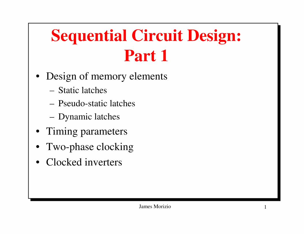
James Morizio 1 Sequential Circuit Design: Part 1 • Design of memory elements – Static latches – Pseudo-static latches – Dynamic latches • Timing parameters • Two-phase clocking • Clocked inverters
Transcript of Sequential Circuit Design: Part...
James Morizio 1
Sequential Circuit Design: Part 1
• Design of memory elements– Static latches– Pseudo-static latches– Dynamic latches
• Timing parameters• Two-phase clocking• Clocked inverters
James Morizio 2
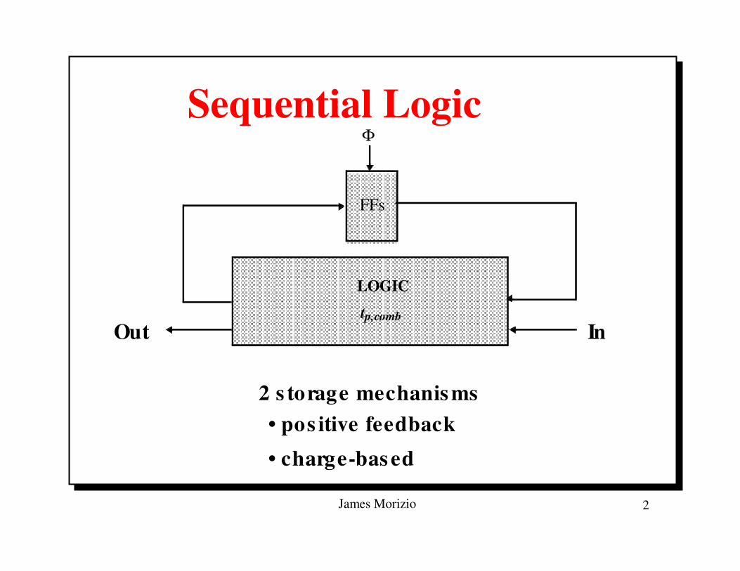
Sequential Logic
2 s torage mechanis ms• pos itive feedback• charge-bas ed
Φ
LOGIC
tp,combInOut
FFs
James Morizio 3
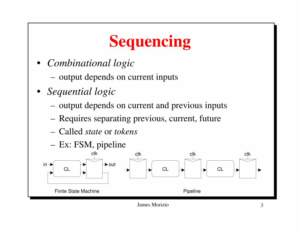
Sequencing• Combinational logic
– output depends on current inputs
• Sequential logic– output depends on current and previous inputs– Requires separating previous, current, future– Called state or tokens– Ex: FSM, pipeline
CL
clk
in out
clk clk clk
CL CL
PipelineFinite State Machine
James Morizio 4
Sequencing Cont.
• If tokens moved through pipeline at constant speed, no sequencing elements would be necessary
• Ex: fiber-optic cable– Light pulses (tokens) are sent down cable– Next pulse sent before first reaches end of cable– No need for hardware to separate pulses– But dispersion sets min time between pulses
• This is called wave pipelining in circuits• In most circuits, dispersion is high
– Delay fast tokens so they don’t catch slow ones.
James Morizio 5
Sequencing Overhead
• Use flip-flops to delay fast tokens so they move through exactly one stage each cycle.
• Inevitably adds some delay to the slow tokens• Makes circuit slower than just the logic delay
– Called sequencing overhead
• Some people call this clocking overhead– But it applies to asynchronous circuits too– Inevitable side effect of maintaining sequence
James Morizio 6
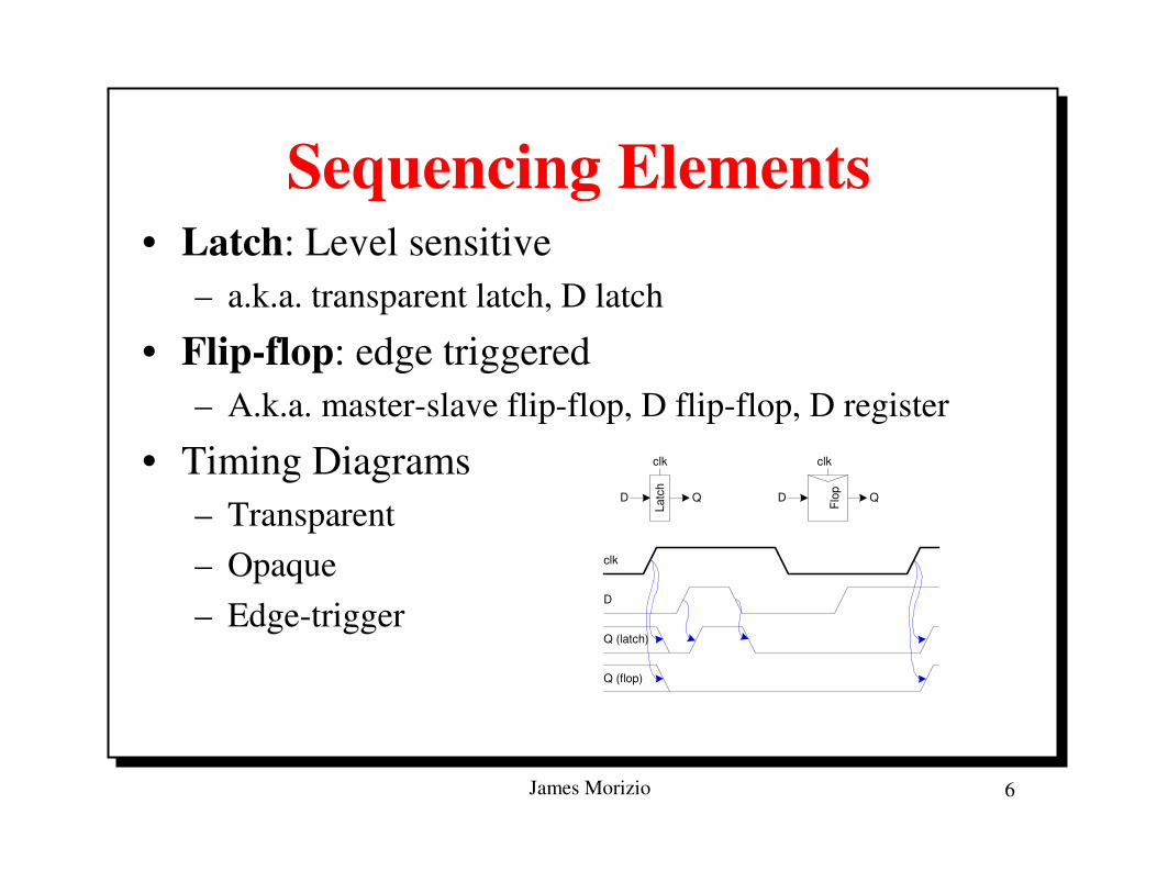
Sequencing Elements• Latch: Level sensitive
– a.k.a. transparent latch, D latch
• Flip-flop: edge triggered– A.k.a. master-slave flip-flop, D flip-flop, D register
• Timing Diagrams– Transparent– Opaque– Edge-trigger
D
Flop
Latc
h
Q
clk clk
D Q
clk
D
Q (latch)
Q (flop)
James Morizio 7
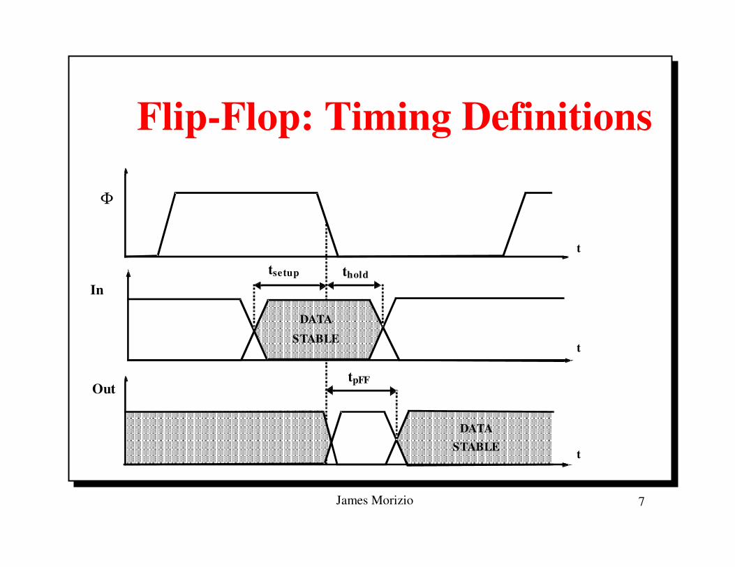
Flip-Flop: Timing Definitions
DATASTABLE
In
t
tsetup thold
DATASTABLE
Out
t
tpFF
t
Φ
James Morizio 8
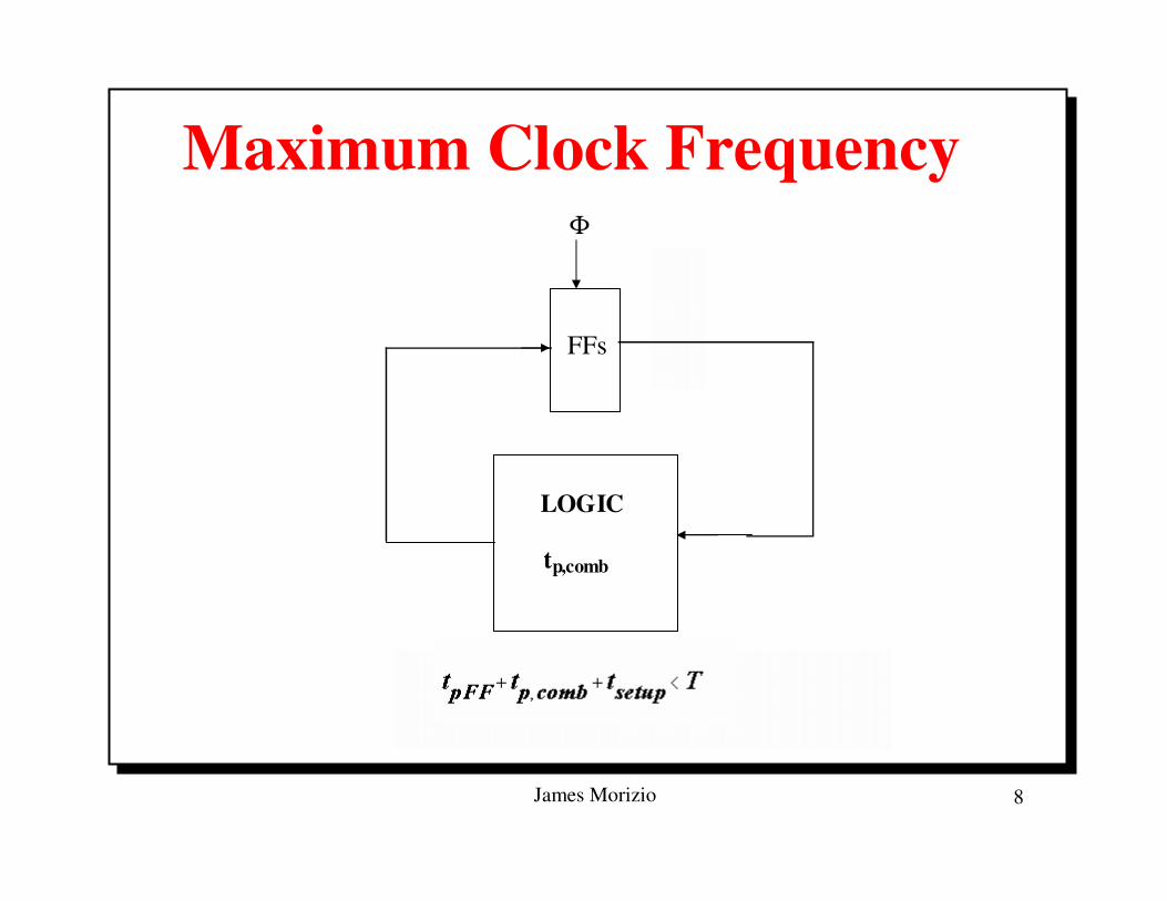
Maximum Clock Frequency
LOGIC
tp,comb
FFs
Φ
James Morizio 9
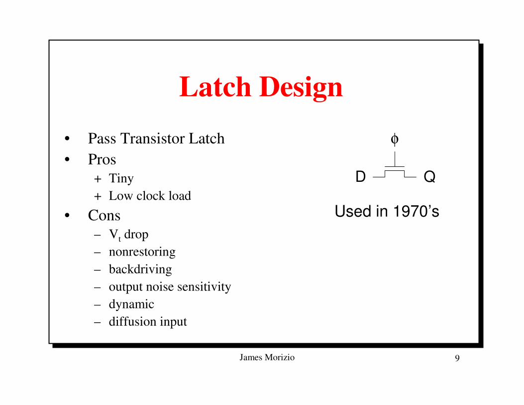
Latch Design• Pass Transistor Latch• Pros
+ Tiny+ Low clock load
• Cons– Vt drop– nonrestoring– backdriving– output noise sensitivity– dynamic– diffusion input
D Q
φ
Used in 1970’s
James Morizio 10
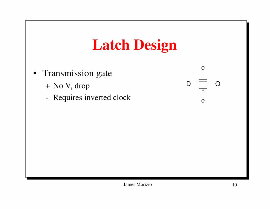
Latch Design
• Transmission gate+ No Vt drop- Requires inverted clock
D Q
φ
φ
James Morizio 11
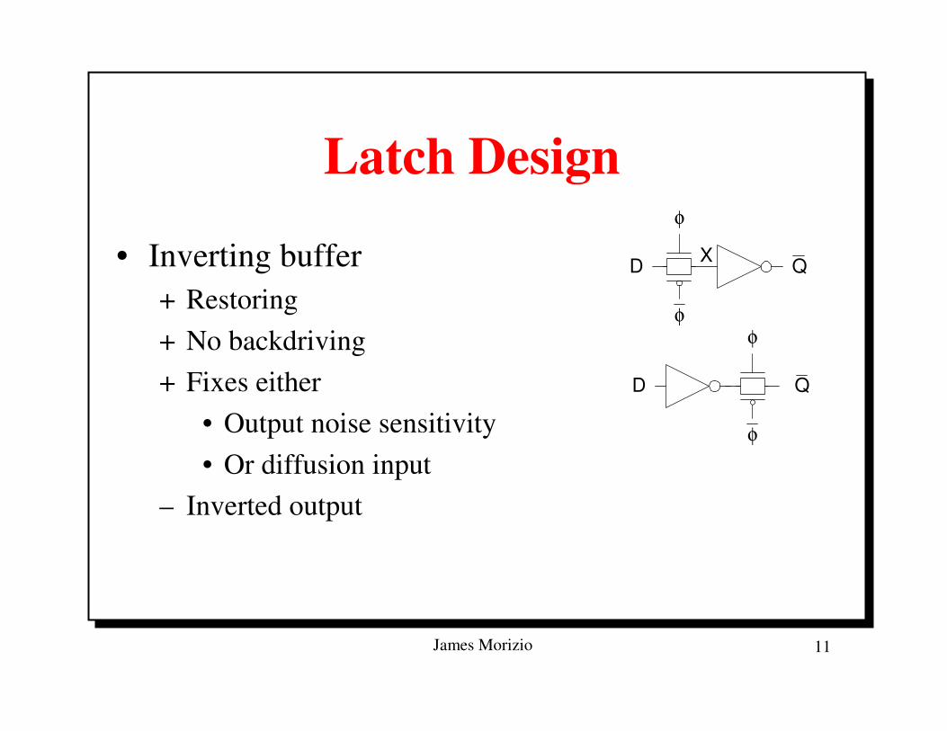
Latch Design
• Inverting buffer+ Restoring+ No backdriving+ Fixes either
• Output noise sensitivity• Or diffusion input
– Inverted output
D
φ
φ
X Q
D Q
φ
φ
James Morizio 12
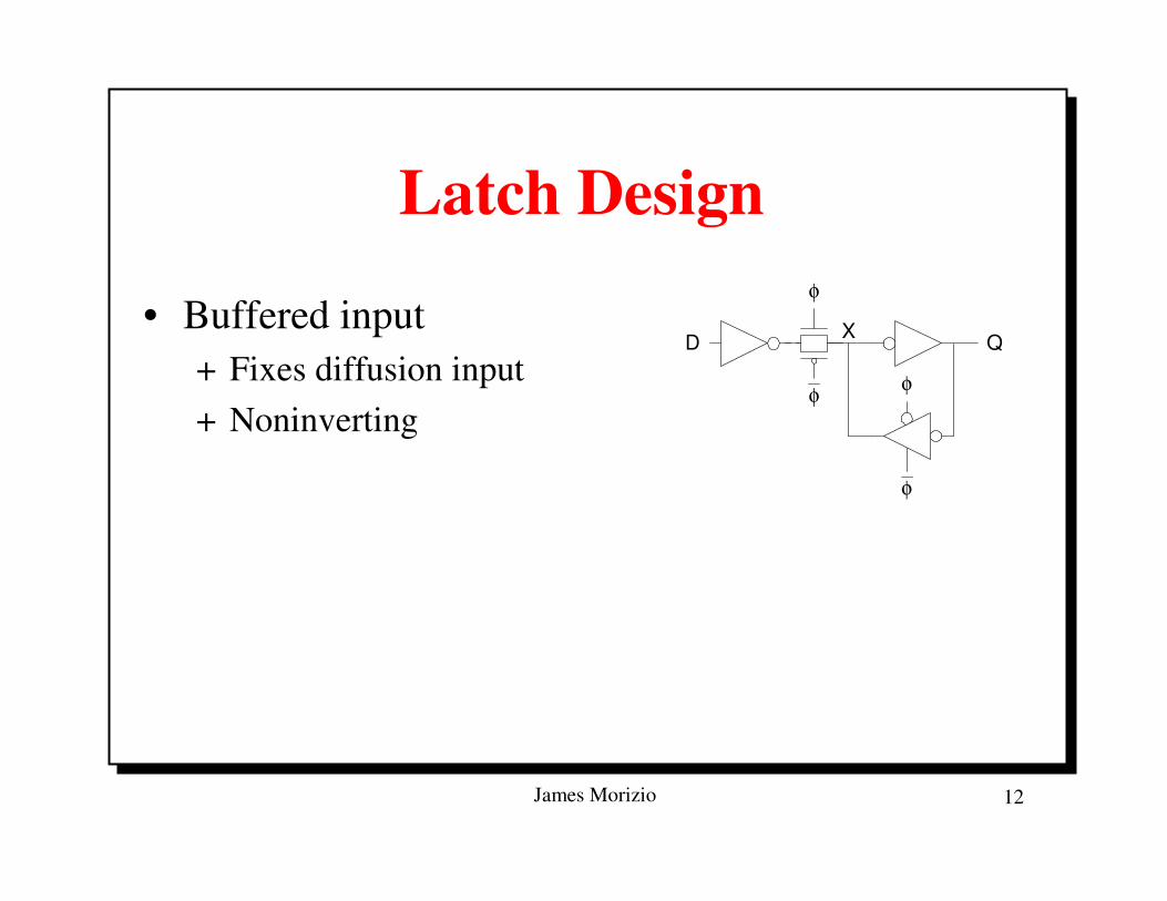
Latch Design
• Buffered input+ Fixes diffusion input+ Noninverting
φ
φ
QD X
φ
φ
James Morizio 13
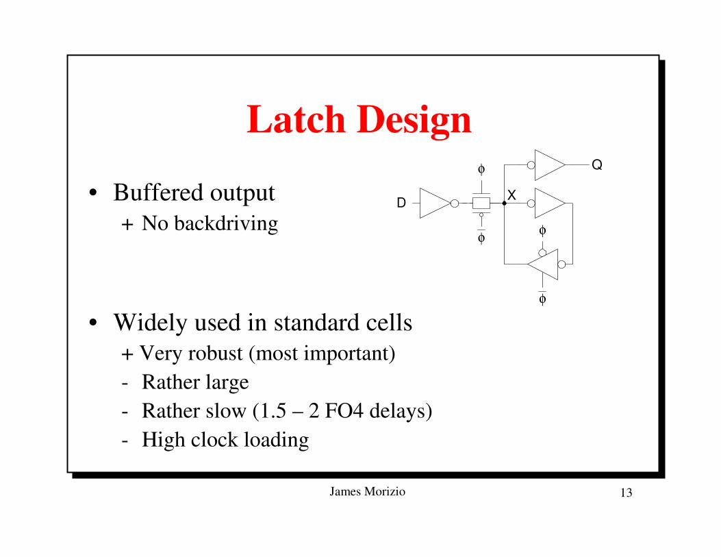
Latch Design
• Buffered output+ No backdriving
• Widely used in standard cells+ Very robust (most important)- Rather large- Rather slow (1.5 – 2 FO4 delays)- High clock loading
φ
φ
Q
D X
φ
φ
James Morizio 14
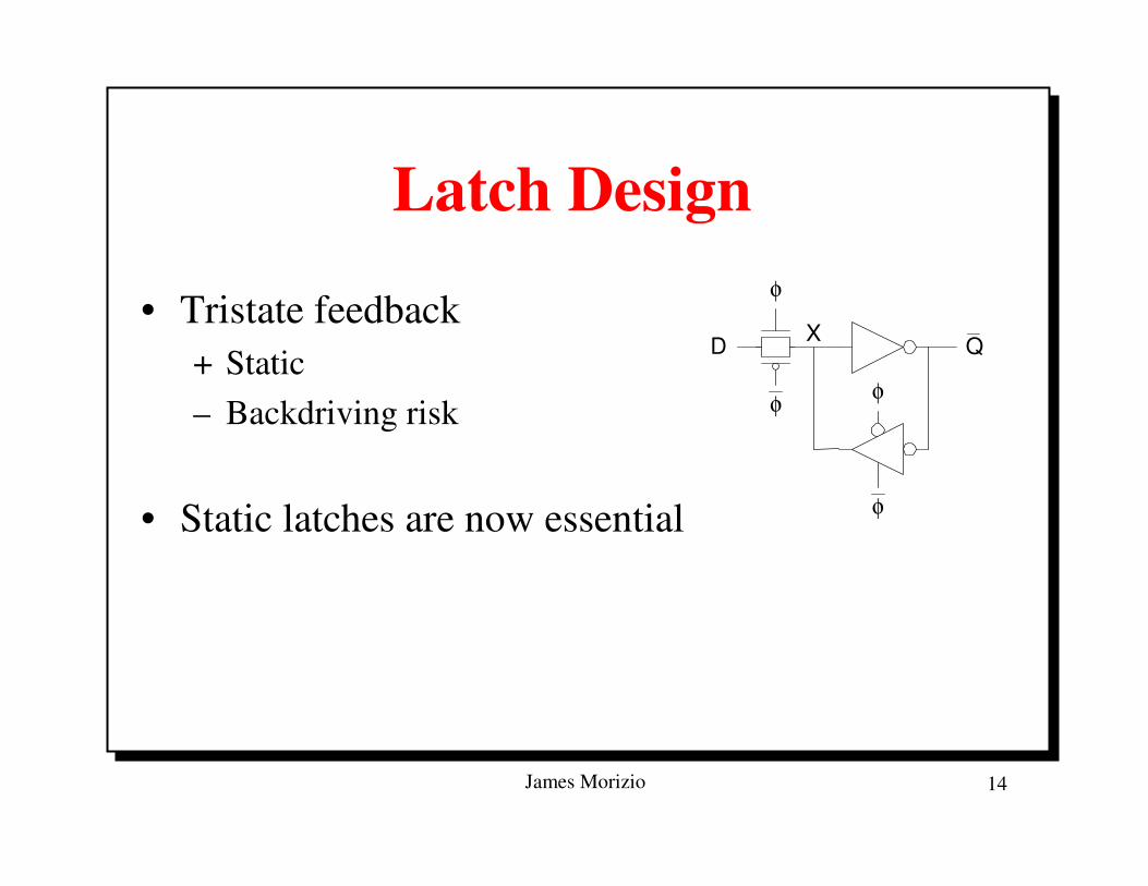
Latch Design
• Tristate feedback+ Static– Backdriving risk
• Static latches are now essential
φ
φ φ
φ
QD X
James Morizio 15
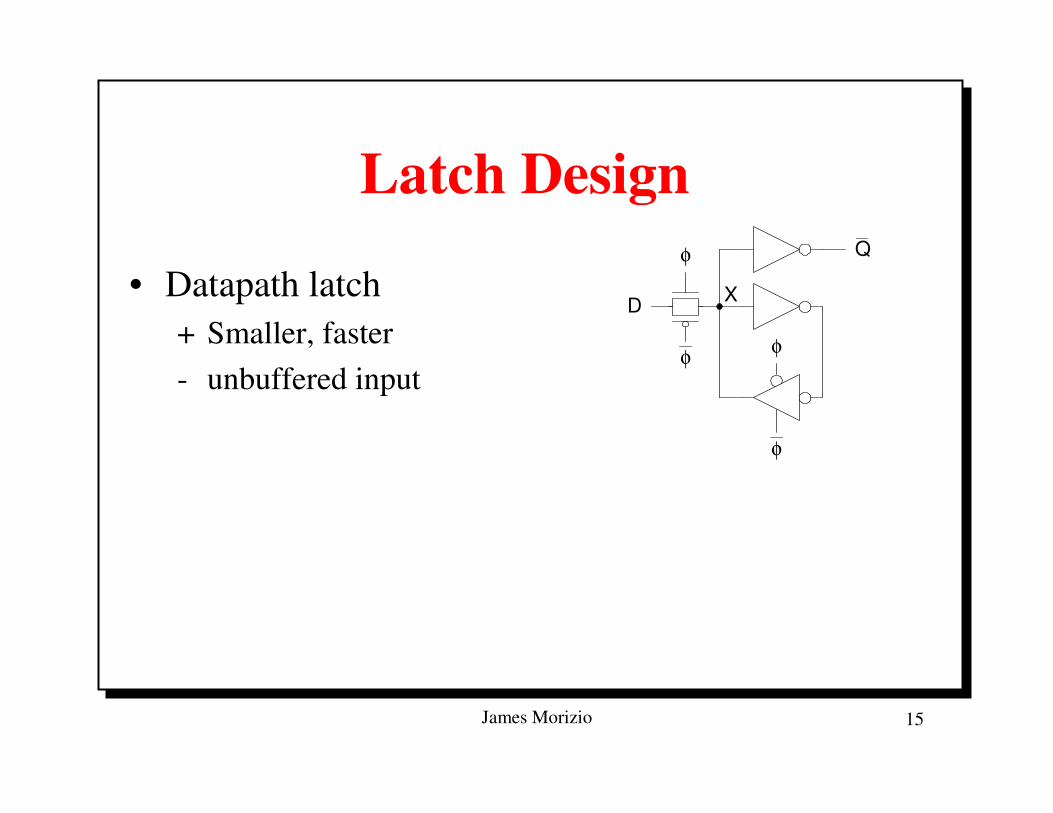
Latch Design
• Datapath latch+ Smaller, faster- unbuffered input
φ
φ φ
φ
Q
D X
James Morizio 16
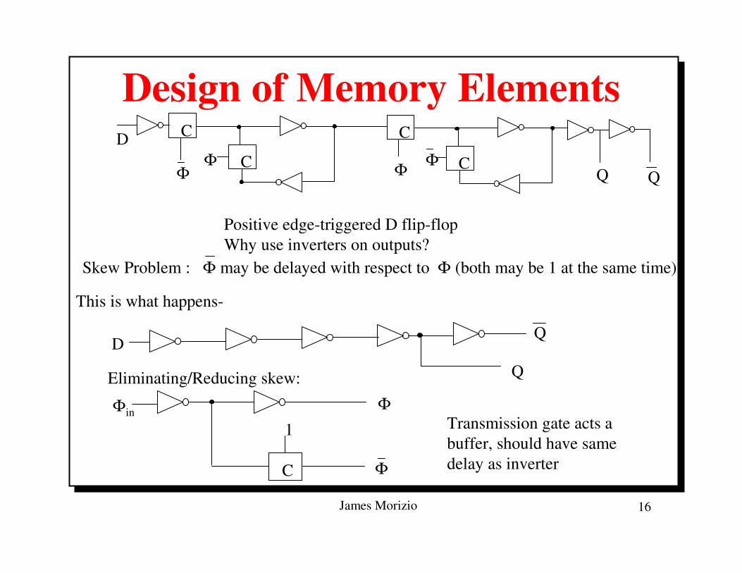
Design of Memory Elements
Q
C
C
C
CD
ΦΦ Φ Φ
Q
Positive edge-triggered D flip-flopWhy use inverters on outputs?
Skew Problem : Φ may be delayed with respect to Φ (both may be 1 at the same time)
This is what happens-
Q
QD
C Φ
ΦΦin
1 Transmission gate acts a buffer, should have samedelay as inverter
Eliminating/Reducing skew:
James Morizio 17
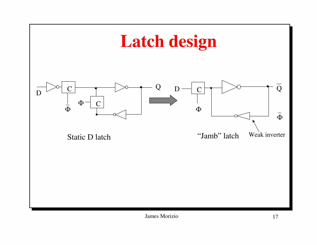
Latch design
Static D latch “Jamb” latch Weak inverter
C
ΦΦ
C
C
D
ΦΦ
DQ Q
James Morizio 18
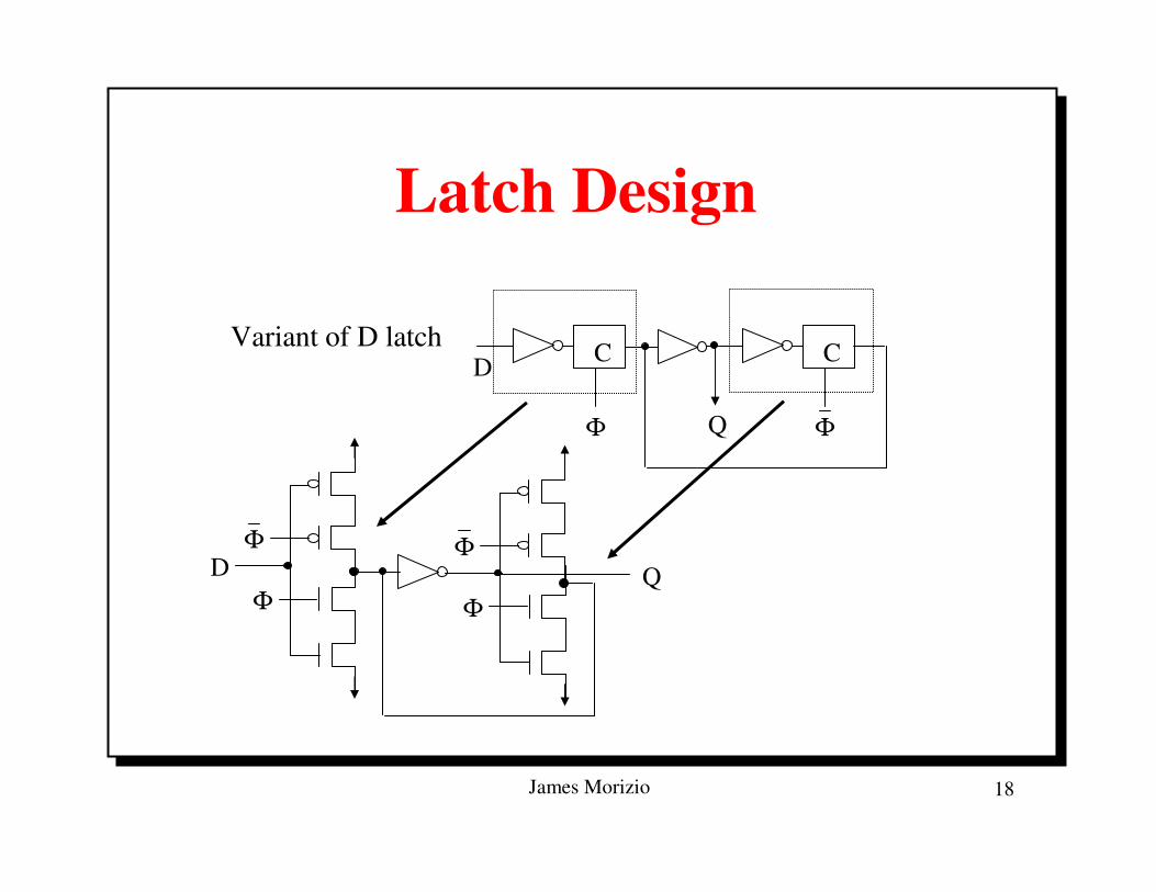
Latch Design
CD
Φ
C
ΦQ
Variant of D latch
Φ
ΦD
Φ
ΦQ
James Morizio 19
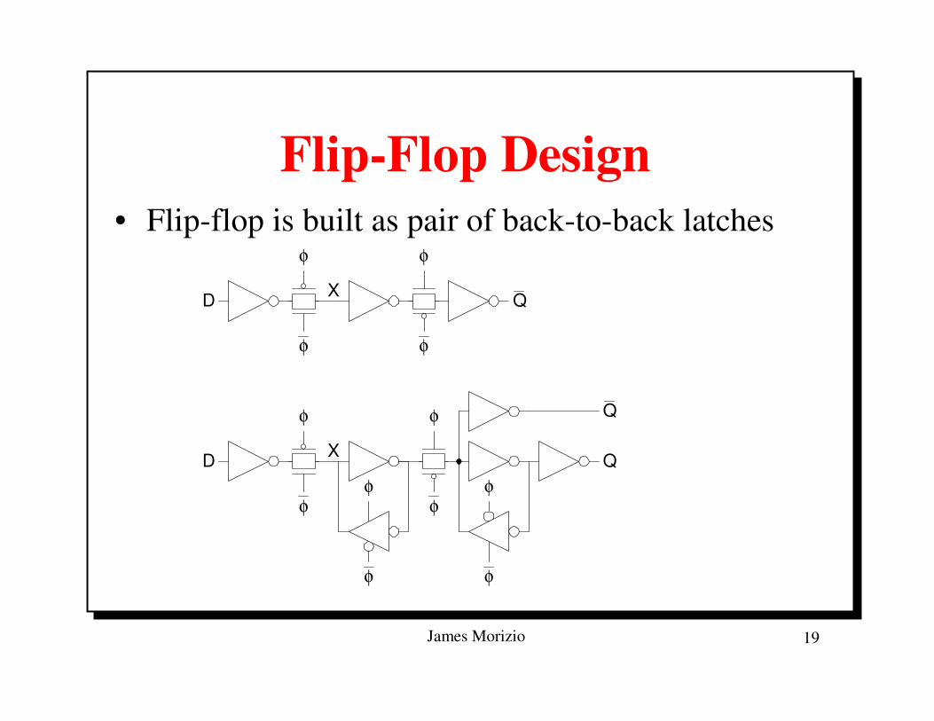
Flip-Flop Design• Flip-flop is built as pair of back-to-back latches
D Q
φ
φ
φ
φ
X
D
φ
φ
φ
φ
X
Q
Qφ
φ
φ
φ

James Morizio 20
Enable• Enable: ignore clock when en = 0
– Mux: increase latch D-Q delay– Clock Gating: increase en setup time, skew
D Q
Latc
h
D Q
en
en
φ
φ
Latc
hDQ
φ
0
1
en
Latc
h
D Q
φ en
DQ
φ
0
1
enD Q
φ en
Flop
Flop
Flop
Symbol Multiplexer Design Clock Gating Design
James Morizio 21
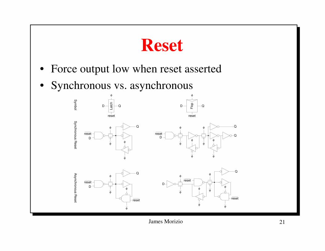
Reset• Force output low when reset asserted• Synchronous vs. asynchronous
D
φ
φ
φ
φ
Q
Qφ
φ
φ
φ
reset
D
φ
φφ
φ
φ
φ
Qφ
φ
Dreset
φ
φ
Qφ
φ
Dreset
reset
φ
φ
reset
Synchronous R
esetA
synchronous Reset
Sym
bol FlopD Q
Latc
h
D Q
reset reset
φ φ
φ
φ
Q
reset
James Morizio 22
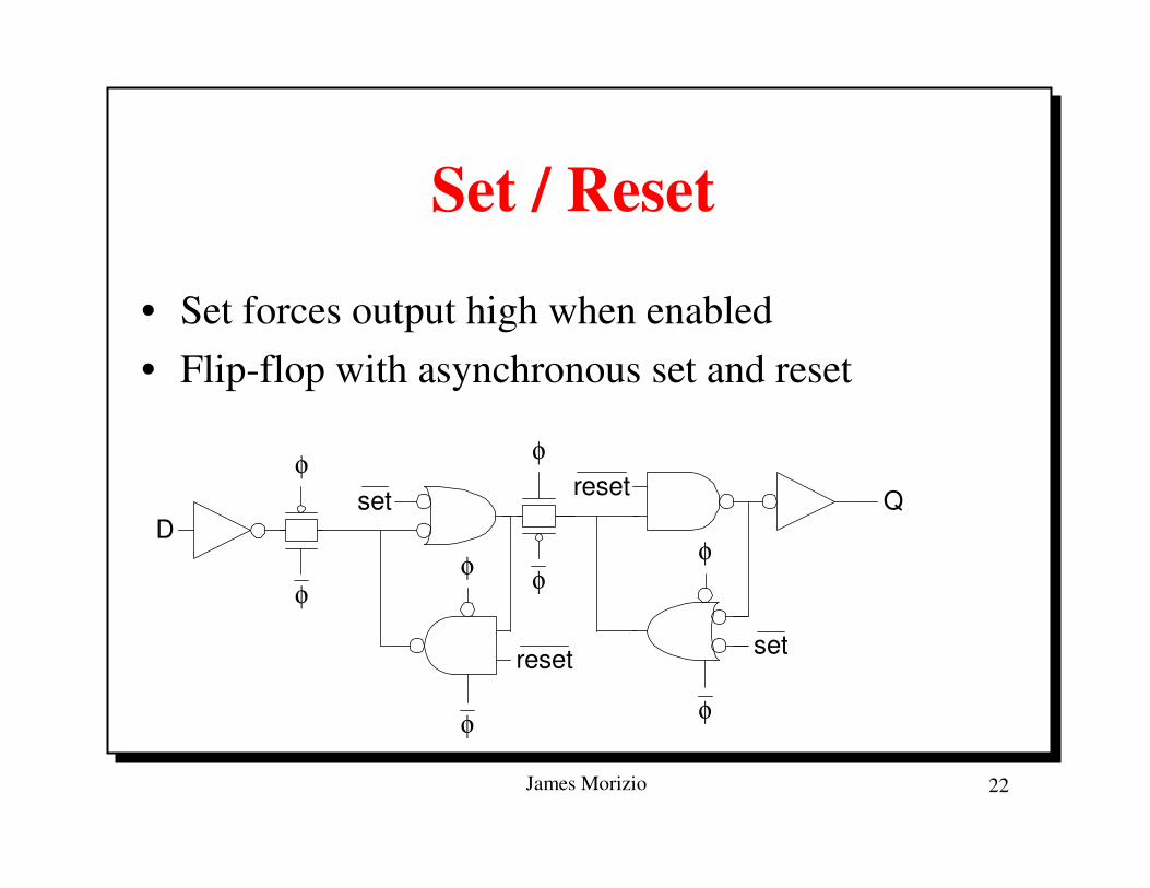
Set / Reset
• Set forces output high when enabled• Flip-flop with asynchronous set and reset
D
φ
φ
φ
φφ
φ
Q
φ
φ
reset
set reset
set
James Morizio 23
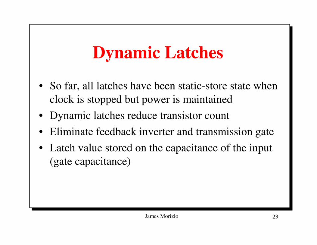
Dynamic Latches
• So far, all latches have been static-store state when clock is stopped but power is maintained
• Dynamic latches reduce transistor count• Eliminate feedback inverter and transmission gate• Latch value stored on the capacitance of the input
(gate capacitance)
James Morizio 24
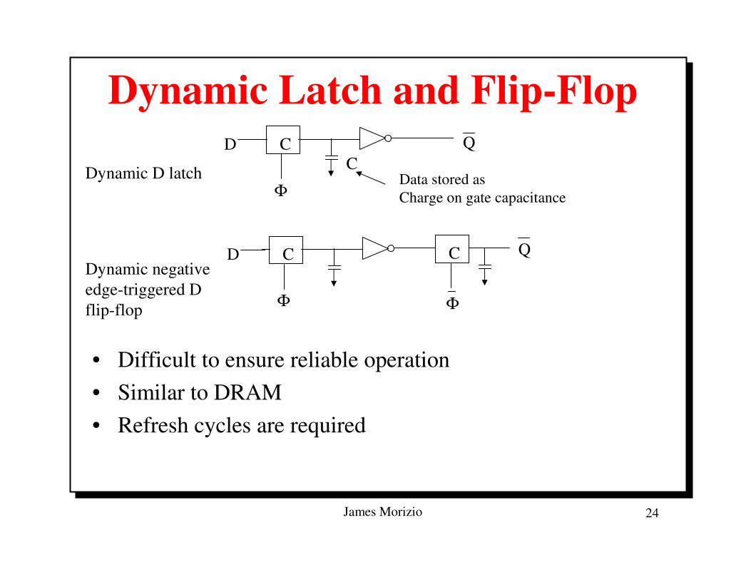
Dynamic Latch and Flip-Flop
• Difficult to ensure reliable operation• Similar to DRAM• Refresh cycles are required
CD
Φ
QC
Data stored asCharge on gate capacitance
Dynamic D latch
Φ
CD
Φ
QDynamic negativeedge-triggered D flip-flop
C
James Morizio 25
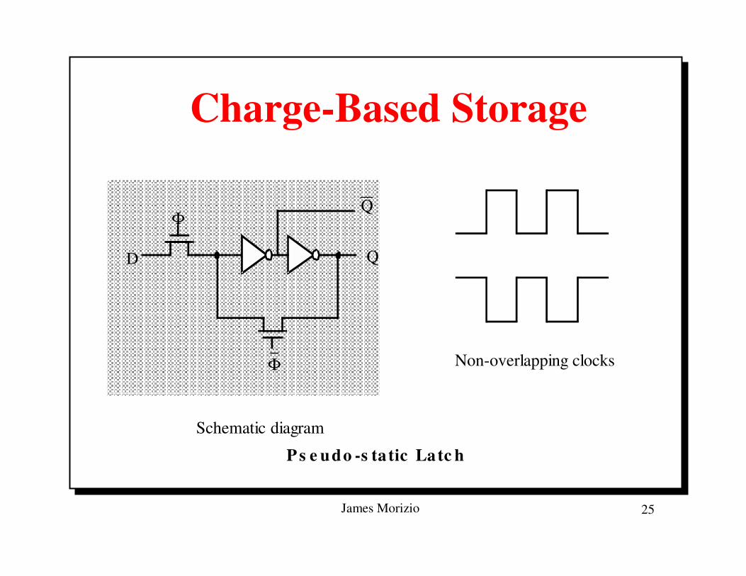
Charge-Based Storage
Schematic diagram
Non-overlapping clocks
P s e udo -s ta tic Latc h
QD
QΦ
Φ
James Morizio 26
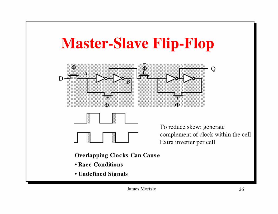
Master-Slave Flip-Flop
AB
Overlapping Clocks Can Caus e• Race Conditions• Undefined Signals
Φ Φ
Φ ΦD
Q
To reduce skew: generatecomplement of clock within the cellExtra inverter per cell
James Morizio 27
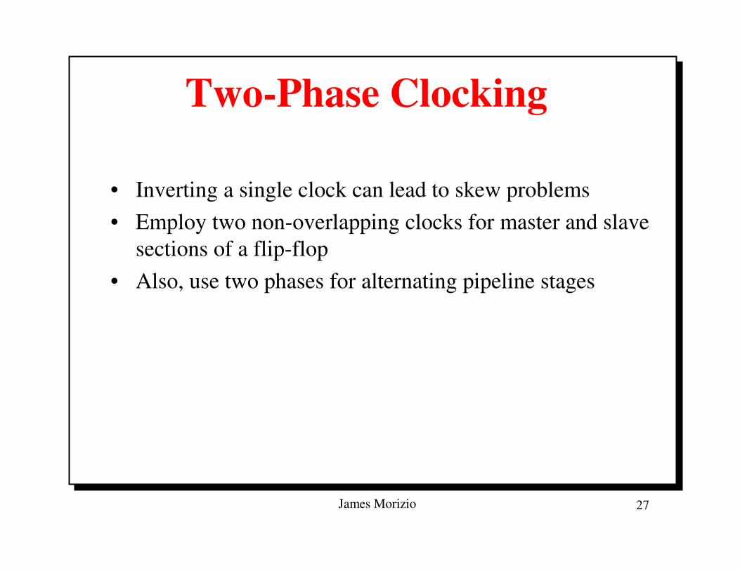
Two-Phase Clocking
• Inverting a single clock can lead to skew problems• Employ two non-overlapping clocks for master and slave
sections of a flip-flop• Also, use two phases for alternating pipeline stages
James Morizio 28
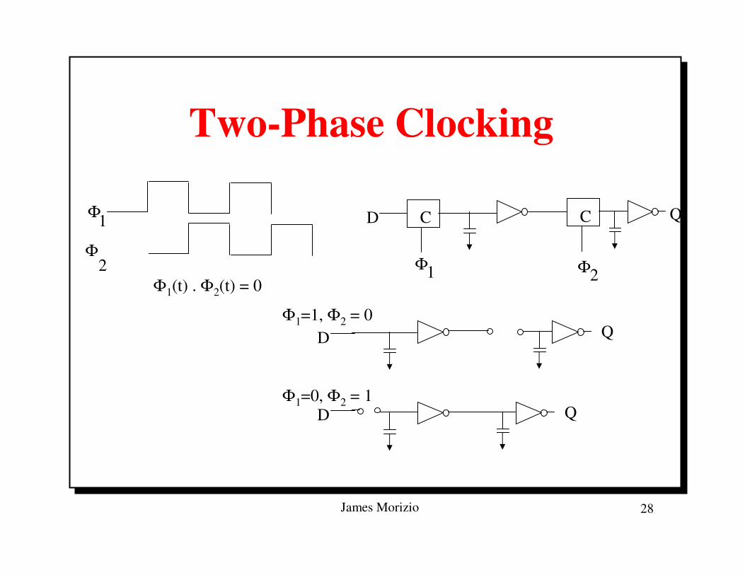
Two-Phase Clocking
Φ1(t) . Φ2(t) = 02
Φ1=1, Φ2 = 0
Φ
Φ
1
2 Φ
CD
Φ
QC
1
D Q
Φ1=0, Φ2 = 1D Q
James Morizio 29
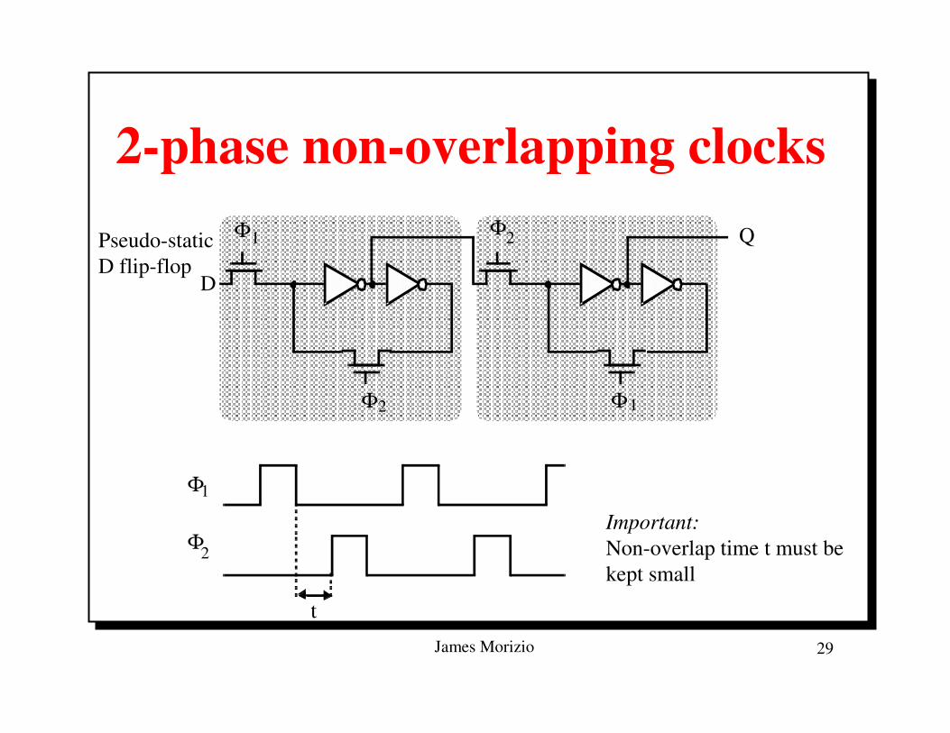
2-phase non-overlapping clocks
1
2
t
Φ
ΦImportant:Non-overlap time t must bekept small
2
1
1
2Φ
Φ
Φ
Φ
Q
D
Pseudo-staticD flip-flop
James Morizio 30
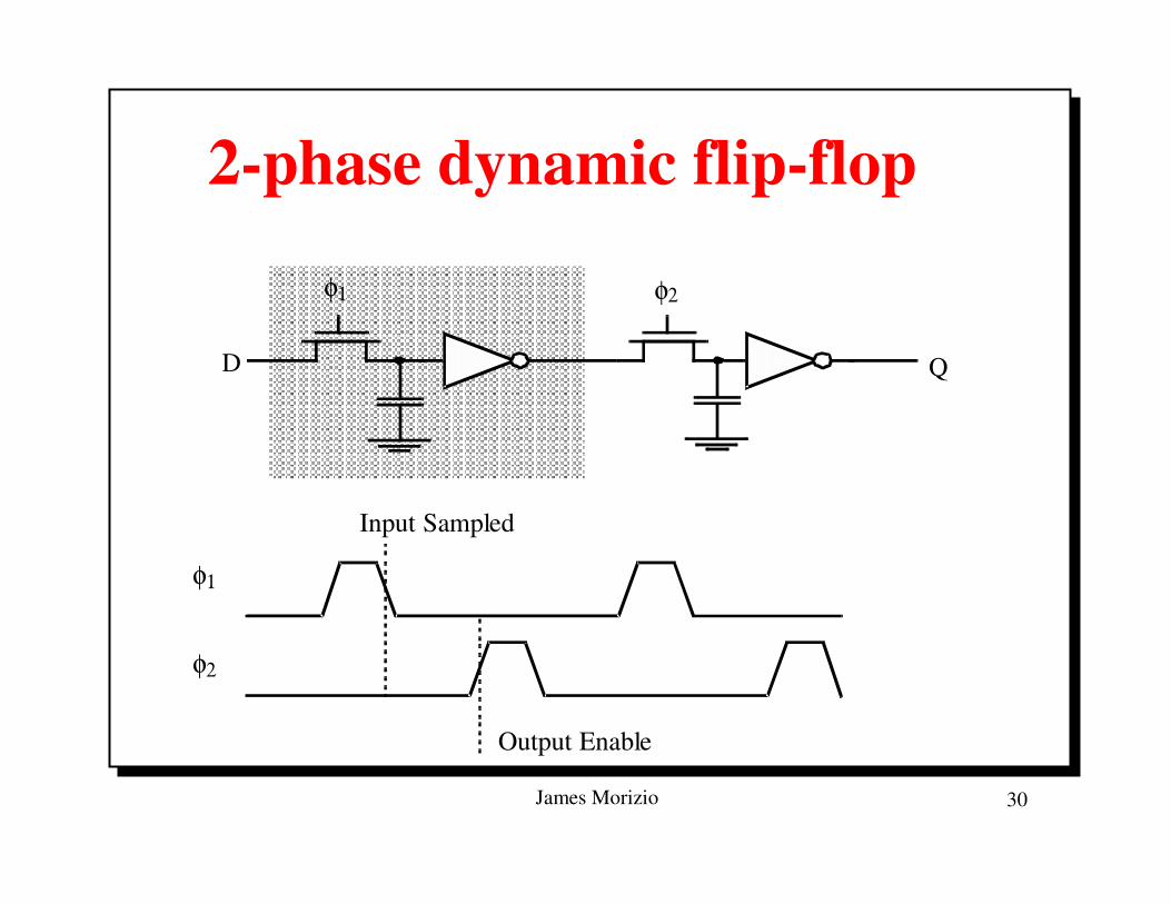
2-phase dynamic flip-flop
φ2φ1
Input Sampled
Output Enable
φ1
φ2
D Q
James Morizio 31
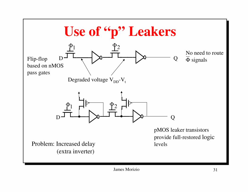
Use of “p” LeakersΦ Φ
Q
Degraded voltage VDD-Vt
Flip-flopbased on nMOSpass gates
1 2
D
Φ Φ
Q
1 2
D
No need to routeΦ signals
pMOS leaker transistorsprovide full-restored logiclevelsProblem: Increased delay
(extra inverter)
James Morizio 32
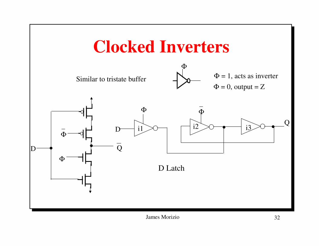
Clocked Inverters
Q
Φ
Similar to tristate buffer Φ = 1, acts as inverterΦ = 0, output = Z
Φ
Φ
D
Φ Φ
i1 i2 i3Q
D
D Latch
James Morizio 33
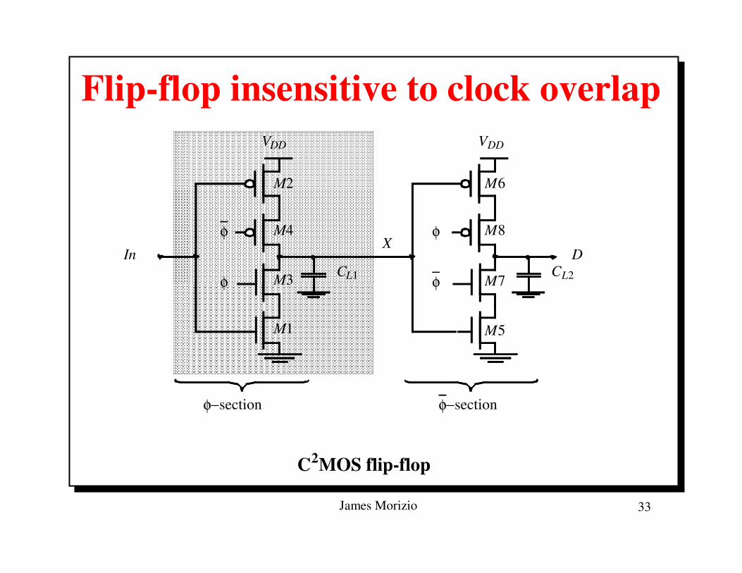
Flip-flop insensitive to clock overlap
DIn
φ
φ φ
φ
VDDVDD
M1
M3
M4
M2 M6
M8
M7
M5
φ−section φ−section
CL1 CL2
X
C2MOS flip-flop
James Morizio 34
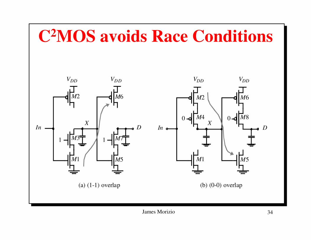
C2MOS avoids Race Conditions
DIn
1
M1
M3
M2 M6
M7
M5
1
DIn
VDDVDD
M1
M4
M2 M6
M8
M5
0 0
VDDVDD
(a) (1-1) overlap (b) (0-0) overlap
X X