SCXI-1193 Specifications - National Instruments
12
SPECIFICATIONS SCXI -1193 500 MHz Quad 8x1 50 Ω Multiplexer This document lists specifications for the SCXI-1193 multiplexer module. All specifications are subject to change without notice. Visit ni.com/manuals for the most current specifications. Configurations .................................................. Quad 8x1 multiplexers Dual 16x1 multiplexers Single 32x1 multiplexer Quad 4x1 terminated multiplexers Dual 8x1 terminated multiplexers Single 16x1 terminated multiplexer Independent RF Performance Characteristics Characteristic impedance (Z 0 ) .......................... 50 Ω, nominal Insertion loss 8x1 DC to 200 MHz ................................ <0.9 dB 200 MHz to 500 MHz....................... <1.6 dB 16x1 DC to 200 MHz ................................ <1.2 dB 200 MHz to 500 MHz....................... <1.9 dB 32x1 DC to 200 MHz ................................ <1.4 dB 200 MHz to 500 MHz....................... <2.4 dB Typical bandwidth (3 dB) 8x1 ............................................................ >900 MHz 16x1 .......................................................... >750 MHz 32x1 .......................................................... >600 MHz ™
Transcript of SCXI-1193 Specifications - National Instruments
SPECIFICATIONS
SCXI -1193500 MHz Quad 8x1 50 Ω Multiplexer
This document lists specifications for the SCXI-1193 multiplexer module. All specifications are subject to change without notice. Visit ni.com/manuals for the most current specifications.
Configurations .................................................. Quad 8x1 multiplexersDual 16x1 multiplexersSingle 32x1 multiplexerQuad 4x1 terminated multiplexersDual 8x1 terminated multiplexersSingle 16x1 terminated multiplexerIndependent
RF Performance CharacteristicsCharacteristic impedance (Z0) .......................... 50 Ω, nominal
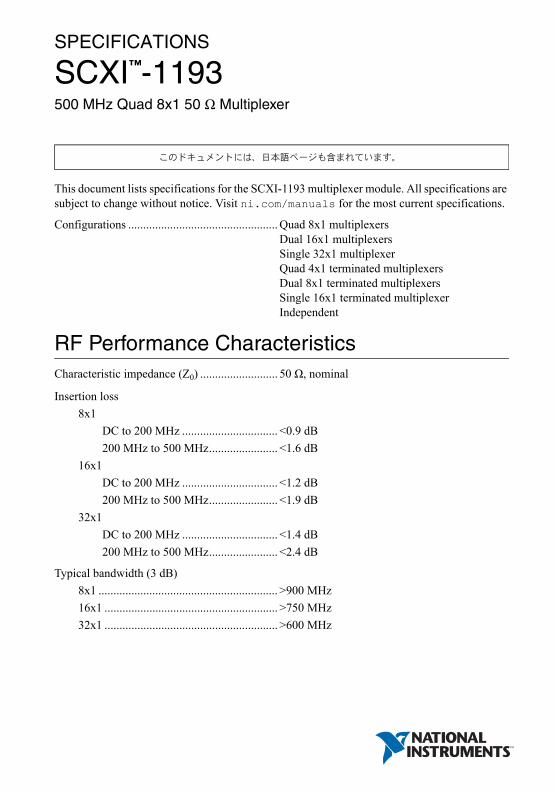
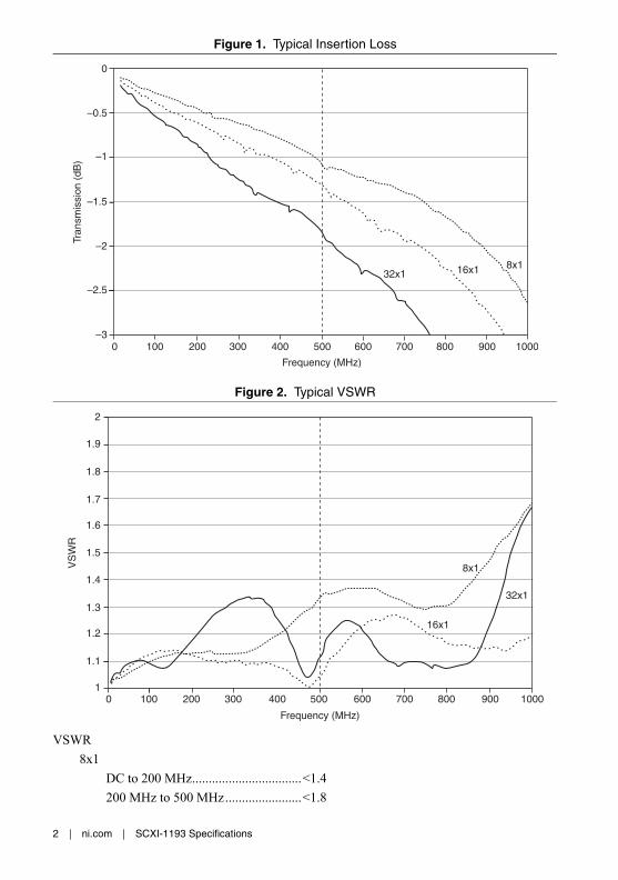
Insertion loss
8x1
DC to 200 MHz ................................ <0.9 dB
200 MHz to 500 MHz....................... <1.6 dB
16x1
DC to 200 MHz ................................ <1.2 dB
200 MHz to 500 MHz....................... <1.9 dB
32x1
DC to 200 MHz ................................ <1.4 dB
200 MHz to 500 MHz....................... <2.4 dB
Typical bandwidth (3 dB)
8x1 ............................................................ >900 MHz
16x1 .......................................................... >750 MHz
32x1 .......................................................... >600 MHz
™
2 | ni.com | SCXI-1193 Specifications
Figure 1. Typical Insertion Loss
Figure 2. Typical VSWR
VSWR
8x1
DC to 200 MHz.................................<1.4
200 MHz to 500 MHz.......................<1.8
0
–0.5
–1
–1.5
–2
–2.5
–30 200 300 400 500 600100 700 800 900 1000
Frequency (MHz)
Tran
smis
sion
(dB
)
32x1 16x1 8x1
2
1.8
1.6
1.5
1.3
1.2
10 200 300 400 500 600100 700 800 900 1000
1.9
1.7
1.4
1.1
Frequency (MHz)
VS
WR
32x1
16x1
8x1
SCXI-1193 Specifications | © National Instruments | 3
16x1
DC to 200 MHz ................................ <1.4
200 MHz to 500 MHz....................... <1.8
32x1
DC to 200 MHz ................................ <1.4
200 MHz to 500 MHz....................... <1.8
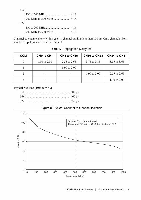
Channel-to-channel skew within each 8-channel bank is less than 100 ps. Only channels from standard topologies are listed in Table 1.
Typical rise time (10% to 90%)
8x1 ............................................................ 385 ps
16x1 .......................................................... 460 ps
32x1 .......................................................... 550 ps
Figure 3. Typical Channel-to-Channel Isolation
Table 1. Propagation Delay (ns)
COM CH0 to CH7 CH8 to CH15 CH16 to CH23 CH24 to CH31
0 1.90 to 2.00 2.55 to 2.65 3.75 to 3.85 3.55 to 3.65
1 — 1.90 to 2.00 — —
2 — — 1.90 to 2.00 2.55 to 2.65
3 — — — 1.90 to 2.00
120
100
80
60
40
20
00 200 300 400 500 600100 700 800 900 1000
Frequency (MHz)
Isol
atio
n (d
B)
Source: CH1, unterminatedMeasured: COM0 CH0, terminated at CH0
4 | ni.com | SCXI-1193 Specifications
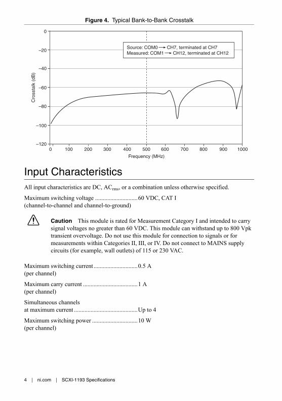
Figure 4. Typical Bank-to-Bank Crosstalk
Input CharacteristicsAll input characteristics are DC, ACrms, or a combination unless otherwise specified.
Maximum switching voltage ............................60 VDC, CAT I(channel-to-channel and channel-to-ground)
Caution This module is rated for Measurement Category I and intended to carry signal voltages no greater than 60 VDC. This module can withstand up to 800 Vpk transient overvoltage. Do not use this module for connection to signals or for measurements within Categories II, III, or IV. Do not connect to MAINS supply circuits (for example, wall outlets) of 115 or 230 VAC.
Maximum switching current .............................0.5 A(per channel)
Maximum carry current ....................................1 A(per channel)
Simultaneous channelsat maximum current ..........................................Up to 4
Maximum switching power ..............................10 W(per channel)
0
–20
–40
–60
–80
–100
–1200 200 300 400 500 600100 700 800 900 1000
Frequency (MHz)
Cro
ssta
lk (
dB)
Source: COM0 CH7, terminated at CH7Measured: COM1 CH12, terminated at CH12
SCXI-1193 Specifications | © National Instruments | 5
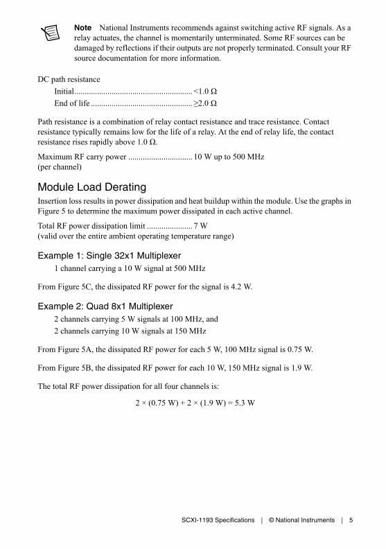
Note National Instruments recommends against switching active RF signals. As a relay actuates, the channel is momentarily unterminated. Some RF sources can be damaged by reflections if their outputs are not properly terminated. Consult your RF source documentation for more information.
DC path resistance
Initial......................................................... <1.0 Ω
End of life .................................................≥2.0 Ω
Path resistance is a combination of relay contact resistance and trace resistance. Contact resistance typically remains low for the life of a relay. At the end of relay life, the contact resistance rises rapidly above 1.0 Ω.
Maximum RF carry power ............................... 10 W up to 500 MHz(per channel)
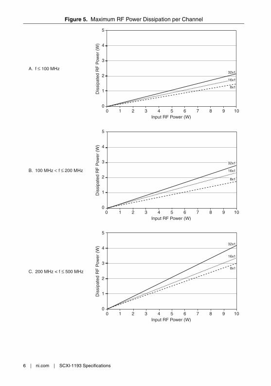
Module Load DeratingInsertion loss results in power dissipation and heat buildup within the module. Use the graphs in Figure 5 to determine the maximum power dissipated in each active channel.
Total RF power dissipation limit ...................... 7 W(valid over the entire ambient operating temperature range)
Example 1: Single 32x1 Multiplexer1 channel carrying a 10 W signal at 500 MHz
From Figure 5C, the dissipated RF power for the signal is 4.2 W.
Example 2: Quad 8x1 Multiplexer2 channels carrying 5 W signals at 100 MHz, and
2 channels carrying 10 W signals at 150 MHz
From Figure 5A, the dissipated RF power for each 5 W, 100 MHz signal is 0.75 W.
From Figure 5B, the dissipated RF power for each 10 W, 150 MHz signal is 1.9 W.
The total RF power dissipation for all four channels is:
2 × (0.75 W) + 2 × (1.9 W) = 5.3 W
6 | ni.com | SCXI-1193 Specifications
Figure 5. Maximum RF Power Dissipation per Channel
32x1
8x1
5
4
3
2
1
00 2 3 4 5 61 7 8 9 10
Input RF Power (W)
Dis
sipa
ted
RF
Pow
er (
W)
5
4
3
2
1
00 2 3 4 5 61 7 8 9 10
Input RF Power (W)
Dis
sipa
ted
RF
Pow
er (
W)
32x1
16x1
8x1
5
4
3
2
1
00 2 3 4 5 61 7 8 9 10
Input RF Power (W)
Dis
sipa
ted
RF
Pow
er (
W)
A. f ≤ 100 MHz
B. 100 MHz < f ≤ 200 MHz
C. 200 MHz < f ≤ 500 MHz
32x1
16x1
16x1
8x1
SCXI-1193 Specifications | © National Instruments | 7
Dynamic CharacteristicsMaximum scan rate .......................................... 100 channels/s
Expected relay life
Mechanical................................................ 50,000,000 cycles
Electrical ................................................... 300,000 cycles(30 V, 0.3 A, DC resistive)
Trigger CharacteristicsInput trigger
Sources...................................................... SCXI trigger lines 0 to 7,Front panel,Rear connector
Minimum pulse width............................... 150 ns
Front panel input voltage
Minimum .......................................... -0.5 V
VL maximum .................................... +0.7 V
VH minimum..................................... +2.0 V
Nominal ............................................ +3.3 V
Maximum.......................................... +5.5 V
Output trigger
Destinations .............................................. SCXI trigger lines 0 to 7, Front panel,Rear connector
Pulse width ............................................... Programmable (1 μs to 62 μs)
Front panel nominal voltage ..................... 3.3 V TTL, 8 mA
Physical CharacteristicsRelay type ......................................................... Electromechanical, latching
Relay contact material ...................................... Silver palladium and gold
I/O connectors................................................... 36 MCX jacks
Trigger connectors ............................................ 2 SMB jacks
SCXI DC power requirement
+5 VDC..................................................... 50 mA
+18.5 VDC to +25 VDC........................... 170 mA
-18.5 VDC to -25 VDC............................. 170 mA
8 | ni.com | SCXI-1193 Specifications
Dimensions (W × H × D)..................................3.0 × 17.3 × 19.8 cm(1.2 × 6.8 × 7.8 in.)
Weight ...............................................................960 g (2 lb 2 oz)
EnvironmentOperating temperature ......................................0 °C to 50 °C
Storage temperature ..........................................-20 °C to 70 °C
Relative humidity..............................................5% to 85% noncondensing
Pollution Degree ...............................................2
Approved at altitudes up to 2,000 m.
Indoor use only.
AccessoriesVisit ni.com for more information about the following accessories.
Table 2. RG-316 Cabling Available for the SCXI-1193
Connectors Length Part Number
MCX-MCX 0.3 m 188374-0R3
1.0 m 188374-01
MCX-BNC 0.3 m 188375-0R3
1.0 m 188375-01
MCX-SMB 0.3 m 188376-0R3
1.0 m 188376-01
MCX-SMA 0.3 m 188377-0R3
1.0 m 188377-01
50 Ω MCX terminator(1 GHz maximum)
— 778831-01
SCXI-1193 Specifications | © National Instruments | 9
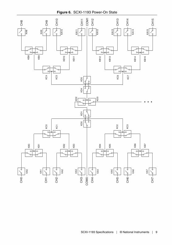
Figure 6. SCXI-1193 Power-On State
CH
7
KA
7
CH
5
CH
6
KA
6
KA
5
CH
3
CO
M0
CH
4
KA
4
KA
3
CH
1
CH
2
KA
2
KA
1
CH
0
KA
0
KB
7
KB
6
KB
5
KB
4
KB
3
KB
2
KB
1
KB
0
KC
3
KC
2
KC
1
KC
0
CH
8
CH
9
CH
10
CH
11
CO
M1
CH
12
CH
13
CH
14
CH
15
KD
0K
D1
KA
15
KA
14
KA
13
KA
12
KA
11
KA
10
KA
9
KA
8
KD
4K
D5
KD
2
KD
3
KB
14
KB
15
KB
12
KB
13
KB
10
KB
11KB
8
KB
9
KC
6
KC
7
KC
4
KC
5
10 | ni.com | SCXI-1193 Specifications
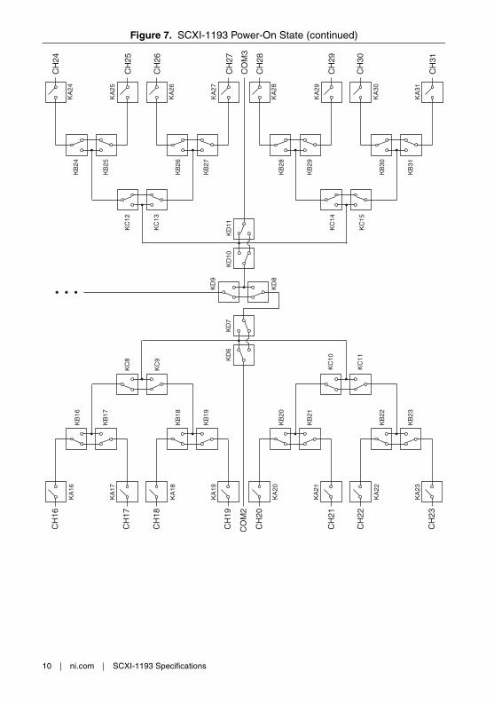
Figure 7. SCXI-1193 Power-On State (continued)
CH
23
KA
23
CH
21
CH
22
KA
22
KA
21
CH
19
CO
M2
CH
20
KA
20
KA
19
CH
17
CH
18
KA
18
KA
17
CH
16
KA
16
KB
23
KB
22
KB
21
KB
20
KB
19
KB
18
KB
17
KB
16
KC
11
KC
10
KC
9
KC
8
CH
24
CH
25
CH
26
CH
27
CO
M3
CH
28
CH
29
CH
30
CH
31
KD
6K
D7
KA
31
KA
30
KA
29
KA
28
KA
27
KA
26
KA
25
KA
24
KD
10K
D11
KD
9
KD
8
KB
30
KB
31
KB
28
KB
29
KB
26
KB
27
KB
24
KB
25
KC
14
KC
15
KC
12
KC
13
SCXI-1193 Specifications | © National Instruments | 11
Compliance and Certifications
SafetyThis product is designed to meet the requirements of the following standards of safety for electrical equipment for measurement, control, and laboratory use:
• IEC 61010-1, EN 61010-1
• UL 61010-1
• CAN/CSA C22.2 No. 61010-1
Note For UL and other safety certifications, refer to the product label or to the Online Product Certification section.
Electromagnetic CompatibilityThis product meets the requirements of the following EMC standards for electrical equipment for measurement, control, and laboratory use:
• EN 61326-1 (IEC 61326-1): Class A emissions; Basic immunity
• EN 55011 (CISPR 11): Group 1, Class A emissions
• FCC 47 CFR Part 15B: Class A emissions
• ICES-001: Class A emissions
Note In the United States (per FCC 47 CFR), Class A equipment is intended for use in commercial, light-industrial, and heavy-industrial locations. In Europe, Canada, Australia, and New Zealand (per CISPR 11), Class A equipment is intended for use only in heavy-industrial locations.
Note Group 1 equipment (per CISPR 11) is any industrial, scientific, or medical equipment that does not intentionally generate radio frequency energy for the treatment of material or inspection/analysis purposes.
Note For EMC declarations and certifications, refer to the Online Product Certification section.
CE ComplianceThis product meets the essential requirements of applicable European Directives, as follows:
Low-Voltage Directive (safety) ........................ 2014/35/EU
Electromagnetic Compatibility Directive (EMC) ............................................... 2014/30/EU
© 2003–2016 National Instruments. All rights reserved.
373460E-01 Sep16
Refer to the NI Trademarks and Logo Guidelines at ni.com/trademarks for more information on NI trademarks. Other product and company names mentioned herein are trademarks or trade names of their respective companies. For patents covering NI products/technology, refer to the appropriate location: Help»Patents in your software, the patents.txt file on your media, or the National Instruments Patents Notice at ni.com/patents. You can find information about end-user license agreements (EULAs) and third-party legal notices in the readme file for your NI product. Refer to the Export Compliance Information at ni.com/legal/export-compliance for the NI global trade compliance policy and how to obtain relevant HTS codes, ECCNs, and other import/export data. NI MAKES NO EXPRESS OR IMPLIED WARRANTIES AS TO THE ACCURACY OF THE INFORMATION CONTAINED HEREIN AND SHALL NOT BE LIABLE FOR ANY ERRORS. U.S. Government Customers: The data contained in this manual was developed at private expense and is subject to the applicable limited rights and restricted data rights as set forth in FAR 52.227-14, DFAR 252.227-7014, and DFAR 252.227-7015.
Online Product CertificationRefer to the product Declaration of Conformity (DoC) for additional regulatory compliance information. To obtain product certifications and the DoC for this product, visit ni.com/certification, search by model number or product line, and click the appropriate link in the Certification column.
Environmental ManagementNI is committed to designing and manufacturing products in an environmentally responsible manner. NI recognizes that eliminating certain hazardous substances from our products is beneficial to the environment and to NI customers.
For additional environmental information, refer to the Minimize Our Environmental Impact web page at ni.com/environment. This page contains the environmental regulations and directives with which NI complies, as well as other environmental information not included in this document.
Waste Electrical and Electronic Equipment (WEEE)EU Customers At the end of the product life cycle, all products must be sent to a WEEE recycling center. For more information about WEEE recycling centers, National Instruments WEEE initiatives, and compliance with WEEE Directive 2002/96/EC on Waste and Electronic Equipment, visit ni.com/environment/weee.
RoHSNational Instruments
(RoHS) National Instruments RoHS ni.com/environment/rohs_china (For information about China RoHS compliance, go to ni.com/environment/rohs_china.)