Robust Low Power VLSI R obust L ow P ower VLSI Synthesizing SRAM timing and Periphery using Synopsis...
23
Robu st Low Powe r VLSI Robust Low Power VLSI Synthesizing SRAM timing and Periphery using Synopsis By: Jim Boley
-
Upload
gavin-barnett -
Category
Documents
-
view
235 -
download
0
Transcript of Robust Low Power VLSI R obust L ow P ower VLSI Synthesizing SRAM timing and Periphery using Synopsis...
Rob
ust
Low
Power
VLSI
Robust
LowPower
VLSI
Synthesizing SRAM timing and Periphery using SynopsisBy: Jim Boley
Rob
ust
Low
Power
VLSI 2
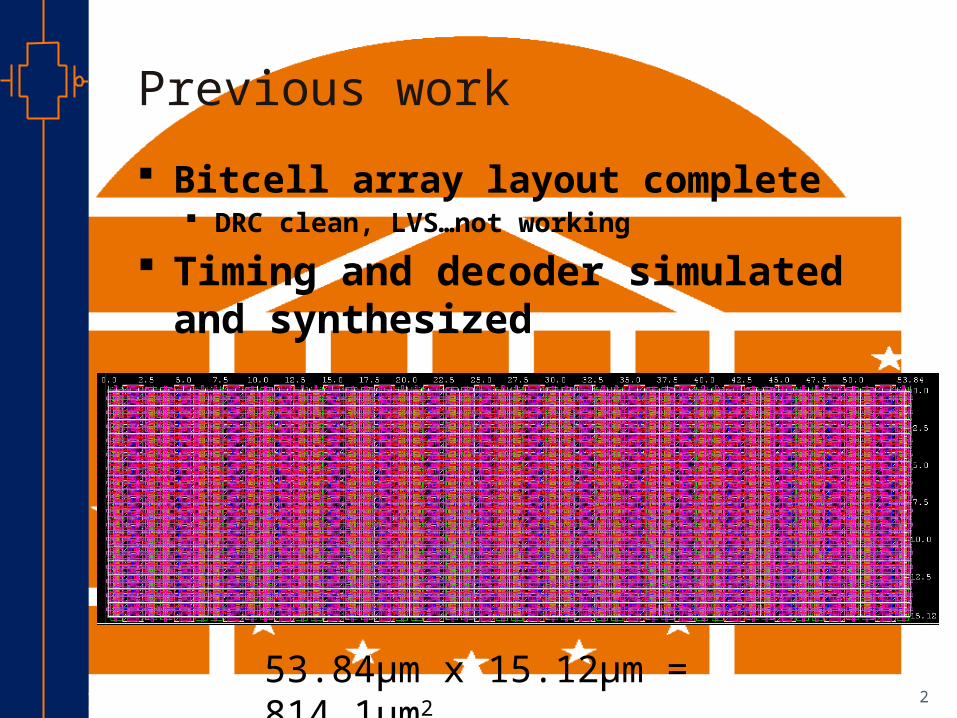
Previous work
53.84μm x 15.12μm = 814.1μm2
Bitcell array layout complete DRC clean, LVS…not working
Timing and decoder simulated and synthesized
Rob
ust
Low
Power
VLSI
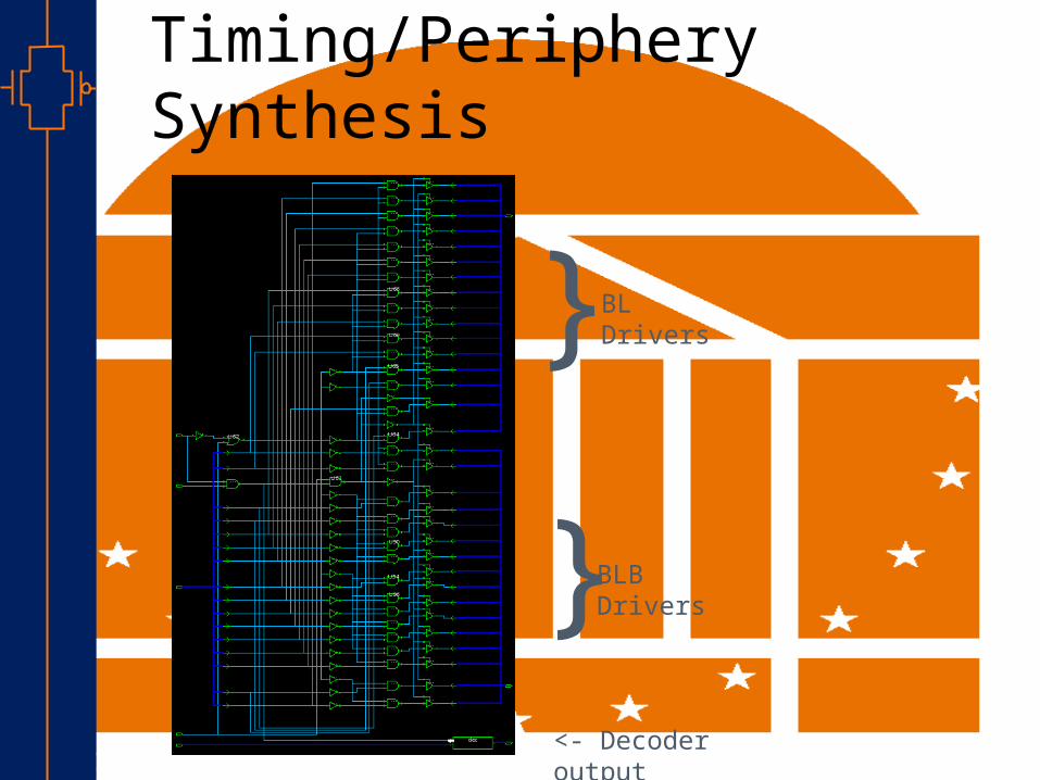
Timing/Periphery Synthesis
}
}
BL Drivers
BLB Drivers
<- Decoder output
Rob
ust
Low
Power
VLSI
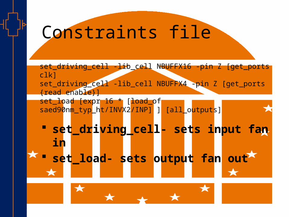
Constraints file
set_driving_cell -lib_cell NBUFFX16 -pin Z [get_ports clk]set_driving_cell -lib_cell NBUFFX4 -pin Z [get_ports {read enable}]set_load [expr 16 * [load_of saed90nm_typ_ht/INVX2/INP] ] [all_outputs]
set_driving_cell- sets input fan in set_load- sets output fan out
Rob
ust
Low
Power
VLSI
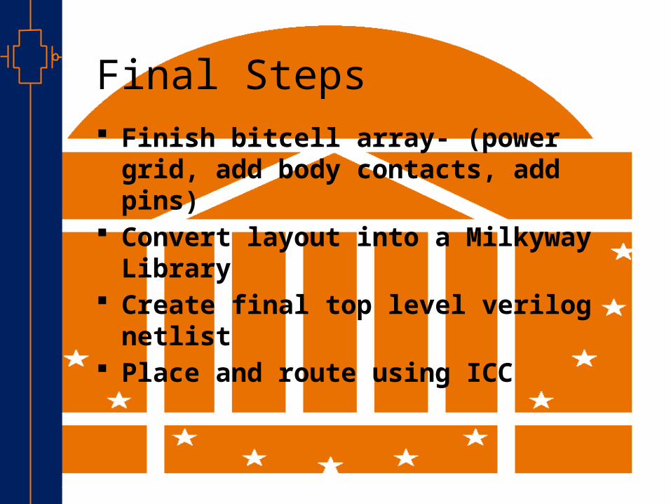
Final Steps Finish bitcell array- (power grid, add body
contacts, add pins) Convert layout into a Milkyway Library Create final top level verilog netlist Place and route using ICC
Rob
ust
Low
Power
VLSI 6
Converting Layout to a Milkyway Library
Rob
ust
Low
Power
VLSI
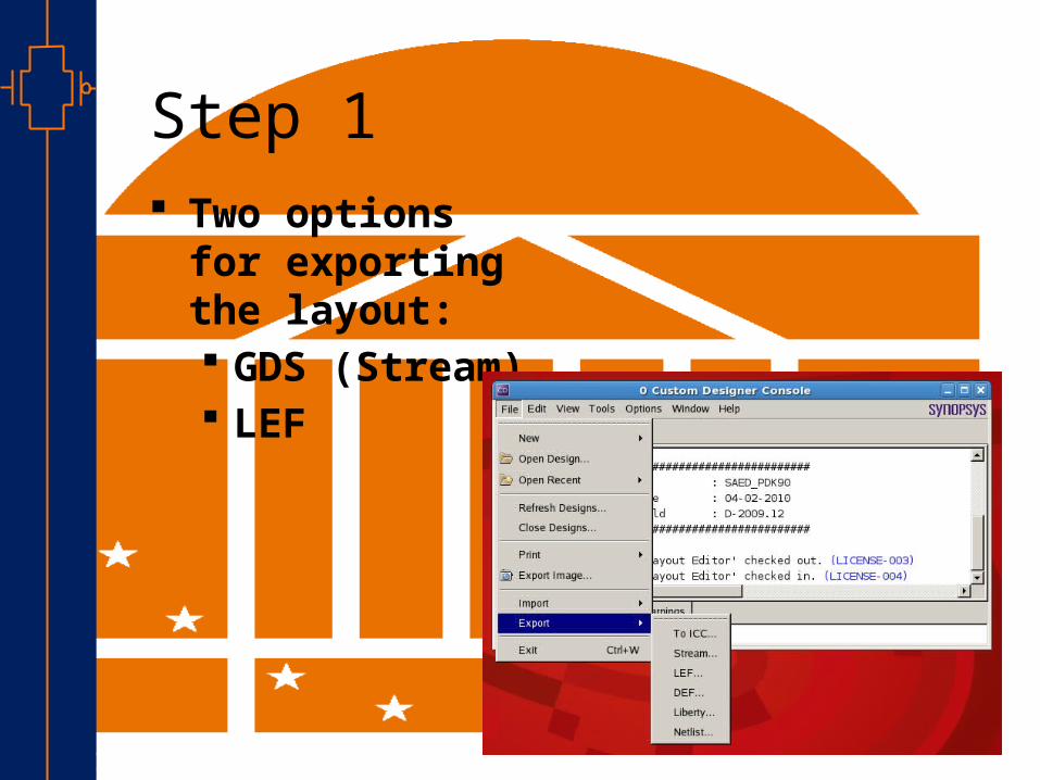
Step 1 Two options for
exporting the layout: GDS (Stream) LEF
Rob
ust
Low
Power
VLSI
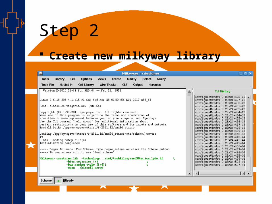
Step 2 Create new milkyway library
Rob
ust
Low
Power
VLSI
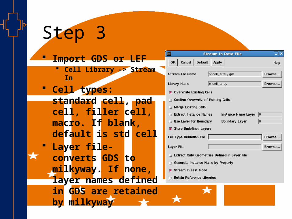
Step 3 Import GDS or LEF
Cell Library -> Stream In
Cell types: standard cell, pad cell, filler cell, macro. If blank, default is std cell
Layer file- converts GDS to milkyway. If none, layer names defined in GDS are retained by milkyway
Rob
ust
Low
Power
VLSI
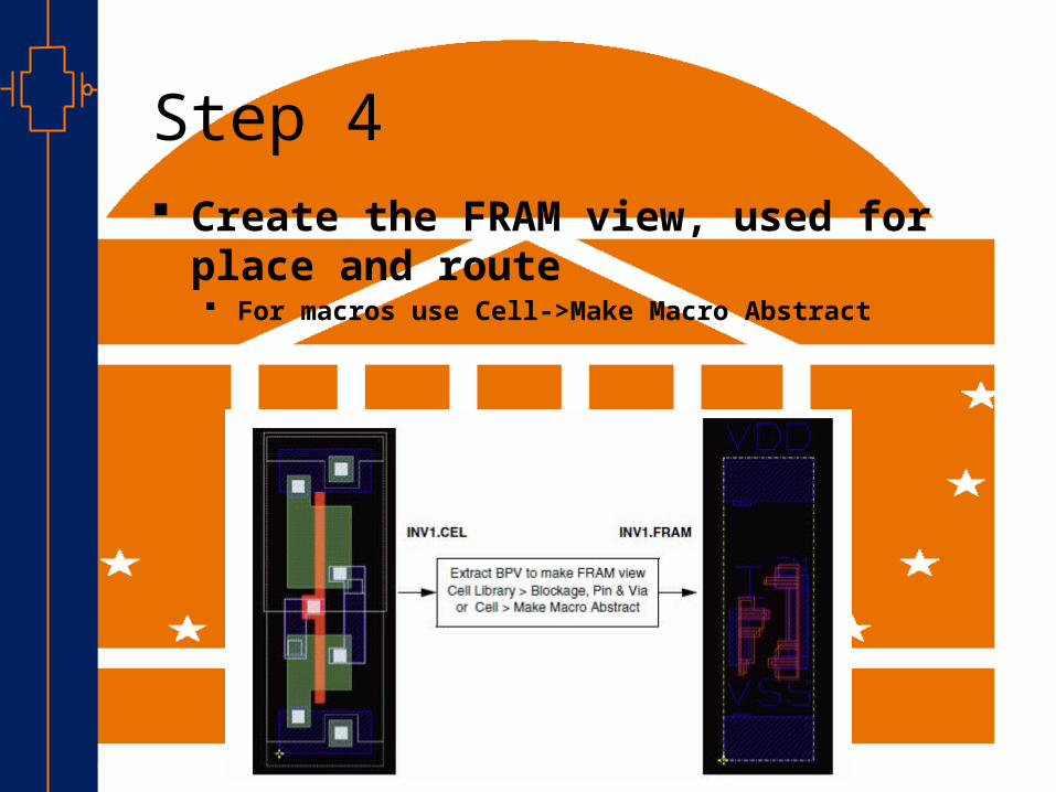
Step 4 Create the FRAM view, used for place and
route For macros use Cell->Make Macro Abstract
Rob
ust
Low
Power
VLSI
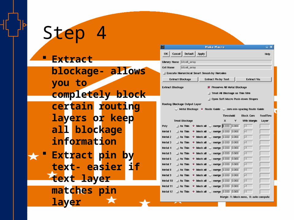
Step 4 Extract blockage-
allows you to completely block certain routing layers or keep all blockage information
Extract pin by text- easier if text layer matches pin layer
Rob
ust
Low
Power
VLSI
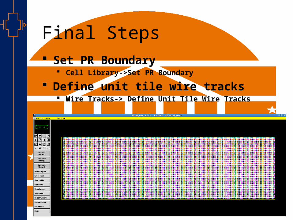
Final Steps Set PR Boundary
Cell Library->Set PR Boundary
Define unit tile wire tracks Wire Tracks-> Define Unit Tile Wire Tracks
Rob
ust
Low
Power
VLSI 13
Run ICC Place and Route
Rob
ust
Low
Power
VLSI
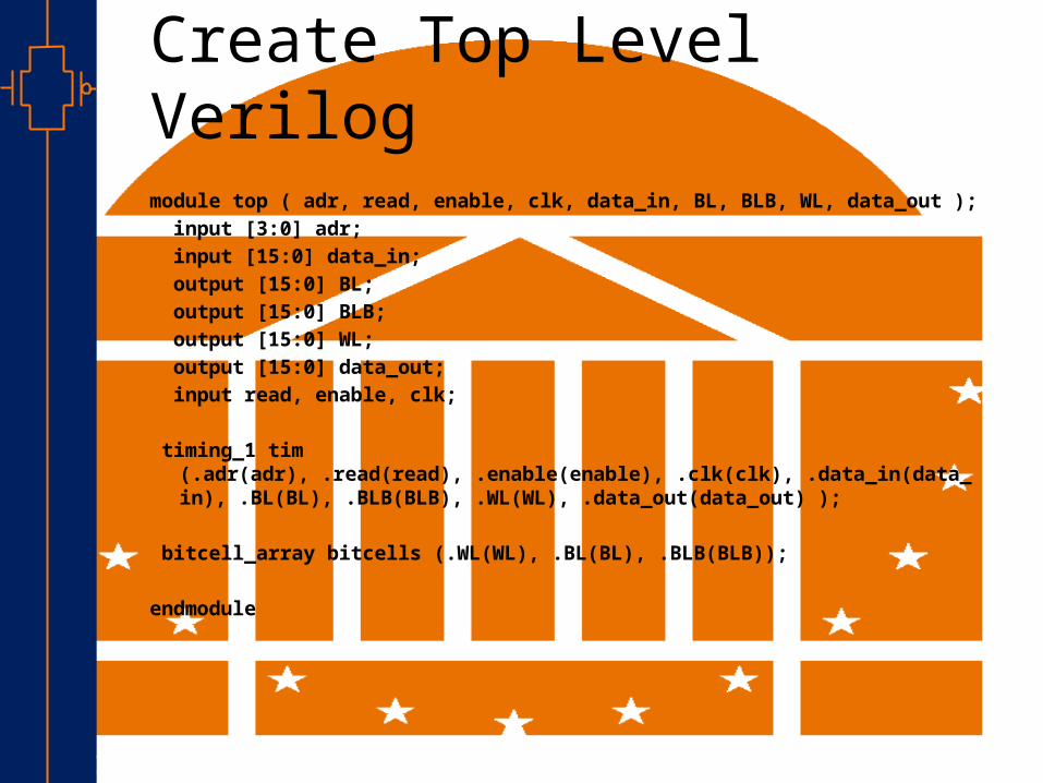
Create Top Level Verilogmodule top ( adr, read, enable, clk, data_in, BL, BLB, WL, data_out ); input [3:0] adr; input [15:0] data_in; output [15:0] BL; output [15:0] BLB; output [15:0] WL; output [15:0] data_out; input read, enable, clk;
timing_1 tim (.adr(adr), .read(read), .enable(enable), .clk(clk), .data_in(data_in), .BL(BL), .BLB(BLB), .WL(WL), .data_out(data_out) );
bitcell_array bitcells (.WL(WL), .BL(BL), .BLB(BLB));
endmodule
Rob
ust
Low
Power
VLSI
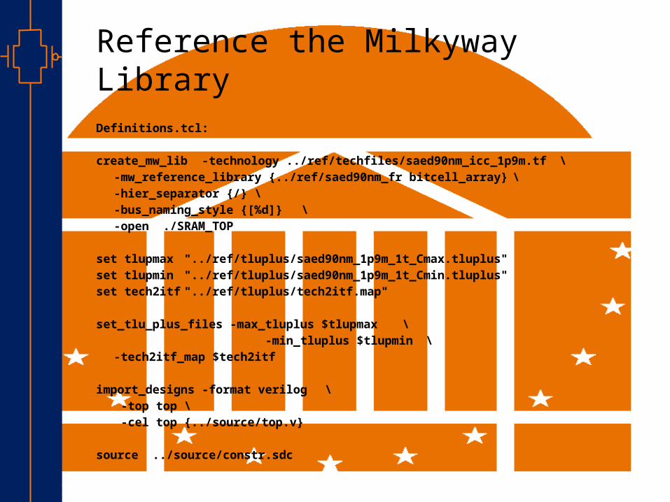
Reference the Milkyway LibraryDefinitions.tcl:
create_mw_lib -technology ../ref/techfiles/saed90nm_icc_1p9m.tf \-mw_reference_library {../ref/saed90nm_fr bitcell_array} \-hier_separator {/} \-bus_naming_style {[%d]} \-open ./SRAM_TOP
set tlupmax "../ref/tluplus/saed90nm_1p9m_1t_Cmax.tluplus"set tlupmin "../ref/tluplus/saed90nm_1p9m_1t_Cmin.tluplus"set tech2itf "../ref/tluplus/tech2itf.map"
set_tlu_plus_files -max_tluplus $tlupmax \ -min_tluplus $tlupmin \
-tech2itf_map $tech2itf
import_designs -format verilog \ -top top \ -cel top {../source/top.v}
source ../source/constr.sdc
Rob
ust
Low
Power
VLSI
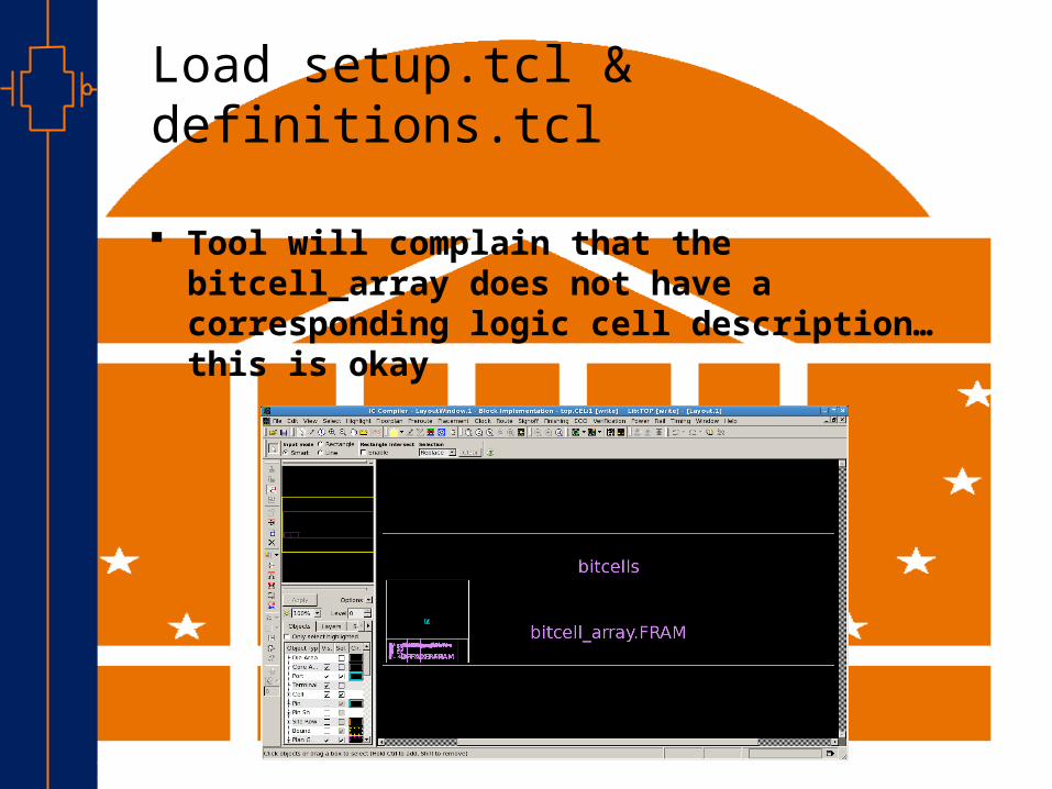
Load setup.tcl & definitions.tcl
Tool will complain that the bitcell_array does not have a corresponding logic cell description…this is okay

Rob
ust
Low
Power
VLSI
Floorplan and power grid created
Rob
ust
Low
Power
VLSI
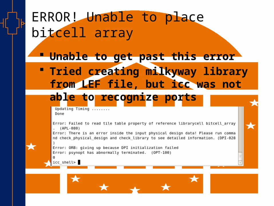
ERROR! Unable to place bitcell array Unable to get past this error Tried creating milkyway library from LEF file,
but icc was not able to recognize ports
Rob
ust
Low
Power
VLSI
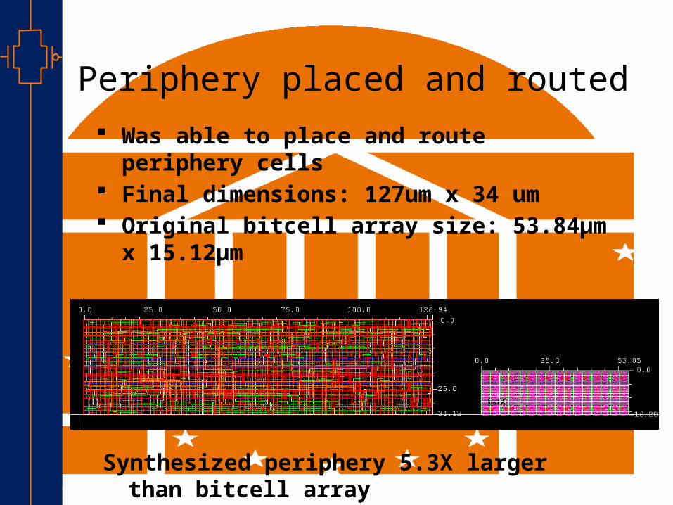
Periphery placed and routed Was able to place and route periphery cells Final dimensions: 127um x 34 um Original bitcell array size: 53.84μm x 15.12μm
Synthesized periphery 5.3X larger than bitcell array
Rob
ust
Low
Power
VLSI
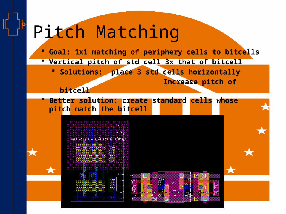
Pitch Matching Goal: 1x1 matching of periphery cells to bitcells Vertical pitch of std cell 3x that of bitcell
Solutions: place 3 std cells horizontally Increase pitch of bitcell
Better solution: create standard cells whose pitch match the bitcell
Rob
ust
Low
Power
VLSI
Conclusions Standard cell library cells are not suited for SRAM
periphery Periphery usually consumes on 20% of total area
because it is pitch matched to the bitcells Place and route tool could be useful for doing top
level routing (assuming placement information could be easily passed to the tool)
Rob
ust
Low
Power
VLSI
Why I didn’t like Synopsys No online forums for answering
questions (like cadence has) Nothing worked the first time
Spent 70% of my time debugging the tool, some problems could not be overcome
Tech support infrastructure not adequate (i.e. working tutorials, wiki FAQs, students with experience)
Conclusion: changing tools = huge start up cost

Rob
ust
Low
Power
VLSI 23
Questions?