![arXiv:2004.11600v1 [cond-mat.mes-hall] 24 Apr 2020 › pdf › 2004.11600.pdfage pulses, focusing on the evolution of excitations due to interactions on the HBT noise signal26,34{36.](https://static.fdocument.org/doc/165x107/60bb2aec00ff5732832e8600/arxiv200411600v1-cond-matmes-hall-24-apr-2020-a-pdf-a-200411600pdf-age.jpg)
RMO4C-2 A Low-Noise 40-GS/s Continuous-Time …sorinv/papers/rfic_06_theo.pdfVAR filter based on a...
4
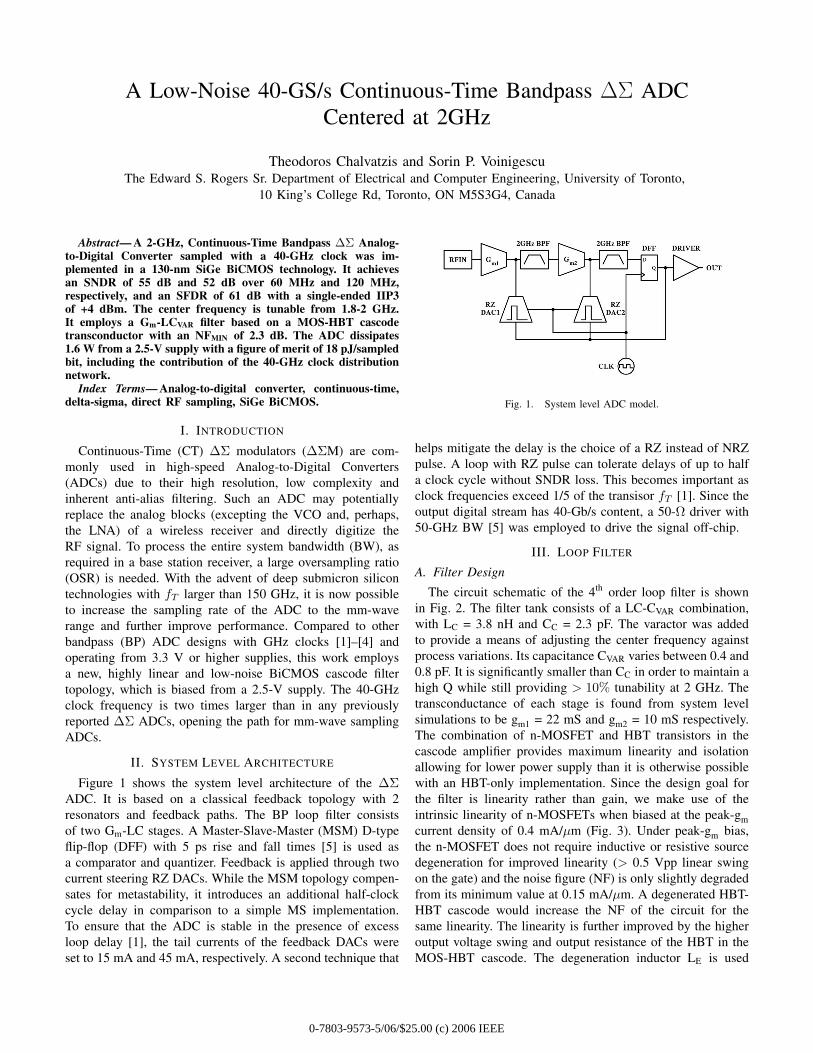
A Low-Noise 40-GS/s Continuous-Time Bandpass ∆Σ ADC Centered at 2GHz Theodoros Chalvatzis and Sorin P. Voinigescu The Edward S. Rogers Sr. Department of Electrical and Computer Engineering, University of Toronto, 10 King’s College Rd, Toronto, ON M5S3G4, Canada Abstract— A 2-GHz, Continuous-Time Bandpass ∆Σ Analog- to-Digital Converter sampled with a 40-GHz clock was im- plemented in a 130-nm SiGe BiCMOS technology. It achieves an SNDR of 55 dB and 52 dB over 60 MHz and 120 MHz, respectively, and an SFDR of 61 dB with a single-ended IIP3 of +4 dBm. The center frequency is tunable from 1.8-2 GHz. It employs a Gm-LC VAR filter based on a MOS-HBT cascode transconductor with an NFMIN of 2.3 dB. The ADC dissipates 1.6 W from a 2.5-V supply with a figure of merit of 18 pJ/sampled bit, including the contribution of the 40-GHz clock distribution network. Index Terms— Analog-to-digital converter, continuous-time, delta-sigma, direct RF sampling, SiGe BiCMOS. I. I NTRODUCTION Continuous-Time (CT) ∆Σ modulators (∆ΣM) are com- monly used in high-speed Analog-to-Digital Converters (ADCs) due to their high resolution, low complexity and inherent anti-alias filtering. Such an ADC may potentially replace the analog blocks (excepting the VCO and, perhaps, the LNA) of a wireless receiver and directly digitize the RF signal. To process the entire system bandwidth (BW), as required in a base station receiver, a large oversampling ratio (OSR) is needed. With the advent of deep submicron silicon technologies with f T larger than 150 GHz, it is now possible to increase the sampling rate of the ADC to the mm-wave range and further improve performance. Compared to other bandpass (BP) ADC designs with GHz clocks [1]–[4] and operating from 3.3 V or higher supplies, this work employs a new, highly linear and low-noise BiCMOS cascode filter topology, which is biased from a 2.5-V supply. The 40-GHz clock frequency is two times larger than in any previously reported ∆Σ ADCs, opening the path for mm-wave sampling ADCs. II. SYSTEM LEVEL ARCHITECTURE Figure 1 shows the system level architecture of the ∆Σ ADC. It is based on a classical feedback topology with 2 resonators and feedback paths. The BP loop filter consists of two G m -LC stages. A Master-Slave-Master (MSM) D-type flip-flop (DFF) with 5 ps rise and fall times [5] is used as a comparator and quantizer. Feedback is applied through two current steering RZ DACs. While the MSM topology compen- sates for metastability, it introduces an additional half-clock cycle delay in comparison to a simple MS implementation. To ensure that the ADC is stable in the presence of excess loop delay [1], the tail currents of the feedback DACs were set to 15 mA and 45 mA, respectively. A second technique that Fig. 1. System level ADC model. helps mitigate the delay is the choice of a RZ instead of NRZ pulse. A loop with RZ pulse can tolerate delays of up to half a clock cycle without SNDR loss. This becomes important as clock frequencies exceed 1/5 of the transisor f T [1]. Since the output digital stream has 40-Gb/s content, a 50-Ω driver with 50-GHz BW [5] was employed to drive the signal off-chip. III. LOOP FILTER A. Filter Design The circuit schematic of the 4 th order loop filter is shown in Fig. 2. The filter tank consists of a LC-C VAR combination, with L C = 3.8 nH and C C = 2.3 pF. The varactor was added to provide a means of adjusting the center frequency against process variations. Its capacitance C VAR varies between 0.4 and 0.8 pF. It is significantly smaller than C C in order to maintain a high Q while still providing > 10% tunability at 2 GHz. The transconductance of each stage is found from system level simulations to be g m1 = 22 mS and g m2 = 10 mS respectively. The combination of n-MOSFET and HBT transistors in the cascode amplifier provides maximum linearity and isolation allowing for lower power supply than it is otherwise possible with an HBT-only implementation. Since the design goal for the filter is linearity rather than gain, we make use of the intrinsic linearity of n-MOSFETs when biased at the peak-g m current density of 0.4 mA/μm (Fig. 3). Under peak-g m bias, the n-MOSFET does not require inductive or resistive source degeneration for improved linearity (> 0.5 Vpp linear swing on the gate) and the noise figure (NF) is only slightly degraded from its minimum value at 0.15 mA/μm. A degenerated HBT- HBT cascode would increase the NF of the circuit for the same linearity. The linearity is further improved by the higher output voltage swing and output resistance of the HBT in the MOS-HBT cascode. The degeneration inductor L E is used 0-7803-9573-5/06/$25.00 (c) 2006 IEEE
-
Upload
duongtuyen -
Category
Documents
-
view
217 -
download
4
Transcript of RMO4C-2 A Low-Noise 40-GS/s Continuous-Time …sorinv/papers/rfic_06_theo.pdfVAR filter based on a...
A Low-Noise 40-GS/s Continuous-Time Bandpass ∆Σ ADCCentered at 2GHz
Theodoros Chalvatzis and Sorin P. VoinigescuThe Edward S. Rogers Sr. Department of Electrical and Computer Engineering, University of Toronto,
10 King’s College Rd, Toronto, ON M5S3G4, Canada
Abstract— A 2-GHz, Continuous-Time Bandpass ∆Σ Analog-to-Digital Converter sampled with a 40-GHz clock was im-plemented in a 130-nm SiGe BiCMOS technology. It achievesan SNDR of 55 dB and 52 dB over 60 MHz and 120 MHz,respectively, and an SFDR of 61 dB with a single-ended IIP3of +4 dBm. The center frequency is tunable from 1.8-2 GHz.It employs a Gm-LCVAR filter based on a MOS-HBT cascodetransconductor with an NFMIN of 2.3 dB. The ADC dissipates1.6 W from a 2.5-V supply with a figure of merit of 18 pJ/sampledbit, including the contribution of the 40-GHz clock distributionnetwork.
Index Terms— Analog-to-digital converter, continuous-time,delta-sigma, direct RF sampling, SiGe BiCMOS.
I. INTRODUCTION
Continuous-Time (CT) ∆Σ modulators (∆ΣM) are com-monly used in high-speed Analog-to-Digital Converters(ADCs) due to their high resolution, low complexity andinherent anti-alias filtering. Such an ADC may potentiallyreplace the analog blocks (excepting the VCO and, perhaps,the LNA) of a wireless receiver and directly digitize theRF signal. To process the entire system bandwidth (BW), asrequired in a base station receiver, a large oversampling ratio(OSR) is needed. With the advent of deep submicron silicontechnologies with fT larger than 150 GHz, it is now possibleto increase the sampling rate of the ADC to the mm-waverange and further improve performance. Compared to otherbandpass (BP) ADC designs with GHz clocks [1]–[4] andoperating from 3.3 V or higher supplies, this work employsa new, highly linear and low-noise BiCMOS cascode filtertopology, which is biased from a 2.5-V supply. The 40-GHzclock frequency is two times larger than in any previouslyreported ∆Σ ADCs, opening the path for mm-wave samplingADCs.
II. SYSTEM LEVEL ARCHITECTURE
Figure 1 shows the system level architecture of the ∆ΣADC. It is based on a classical feedback topology with 2resonators and feedback paths. The BP loop filter consistsof two Gm-LC stages. A Master-Slave-Master (MSM) D-typeflip-flop (DFF) with 5 ps rise and fall times [5] is used asa comparator and quantizer. Feedback is applied through twocurrent steering RZ DACs. While the MSM topology compen-sates for metastability, it introduces an additional half-clockcycle delay in comparison to a simple MS implementation.To ensure that the ADC is stable in the presence of excessloop delay [1], the tail currents of the feedback DACs wereset to 15 mA and 45 mA, respectively. A second technique that
Fig. 1. System level ADC model.
helps mitigate the delay is the choice of a RZ instead of NRZpulse. A loop with RZ pulse can tolerate delays of up to halfa clock cycle without SNDR loss. This becomes important asclock frequencies exceed 1/5 of the transisor fT [1]. Since theoutput digital stream has 40-Gb/s content, a 50-Ω driver with50-GHz BW [5] was employed to drive the signal off-chip.
III. LOOP FILTER
A. Filter Design
The circuit schematic of the 4th order loop filter is shownin Fig. 2. The filter tank consists of a LC-CVAR combination,with LC = 3.8 nH and CC = 2.3 pF. The varactor was addedto provide a means of adjusting the center frequency againstprocess variations. Its capacitance CVAR varies between 0.4 and0.8 pF. It is significantly smaller than CC in order to maintain ahigh Q while still providing > 10% tunability at 2 GHz. Thetransconductance of each stage is found from system levelsimulations to be gm1 = 22 mS and gm2 = 10 mS respectively.The combination of n-MOSFET and HBT transistors in thecascode amplifier provides maximum linearity and isolationallowing for lower power supply than it is otherwise possiblewith an HBT-only implementation. Since the design goal forthe filter is linearity rather than gain, we make use of theintrinsic linearity of n-MOSFETs when biased at the peak-gmcurrent density of 0.4 mA/µm (Fig. 3). Under peak-gm bias,the n-MOSFET does not require inductive or resistive sourcedegeneration for improved linearity (> 0.5 Vpp linear swingon the gate) and the noise figure (NF) is only slightly degradedfrom its minimum value at 0.15 mA/µm. A degenerated HBT-HBT cascode would increase the NF of the circuit for thesame linearity. The linearity is further improved by the higheroutput voltage swing and output resistance of the HBT in theMOS-HBT cascode. The degeneration inductor LE is used
0-7803-9573-5/06/$25.00 (c) 2006 IEEE
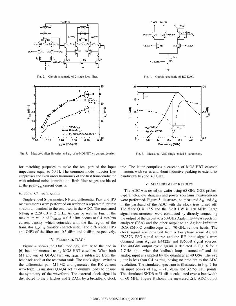
Fig. 2. Circuit schematic of 2-stage loop filter.
Fig. 3. Measured filter linearity and gm of n-MOSFET vs current density.
for matching purposes to make the real part of the inputimpedance equal to 50 Ω. The common mode inductor LEE
suppresses the even order harmonics of the first transconductorwith minimal noise contribution. Both filter stages are biasedat the peak-gm current density.
B. Filter Characterization
Single-ended S-parameter, NF and differential P1dB and IP3measurements were performed on wafer on a separate filter teststructure, identical to the one used in the ADC. The measuredNFMIN is 2.29 dB at 2 GHz. As can be seen in Fig. 3, themaximum value of P1dB,out = 0.5 dBm occurs at 0.4 mA/µmcurrent density, which coincides with the flat region of thetransistor gm-IDS transfer characteristic. The differential IIP3and OIP3 of the filter are -0.5 dBm and 9 dBm, respectively.
IV. FEEDBACK DACS
Figure 4 shows the DAC topology, similar to the one in[6] but implemented using MOS-HBT cascodes. When bothM1 and one of Q1-Q2 turn on, ITAIL is subtracted from thefeedback node at the resonator tank. The clock signal switchesthe differential pair M1-M2 and generates the RZ currentwaveform. Transistors Q3-Q4 act as dummy loads to ensurethe symmetry of the waveform. The external clock signal isdistributed to the 3 latches and 2 DACs by a broadband clock
Fig. 4. Circuit schematic of RZ DAC.
Fig. 5. Measured ADC single-ended S-parameters.
tree. The latter comprises a cascade of MOS-HBT cascodeinverters with series and shunt inductive peaking to extend itsbandwidth beyond 40 GHz.
V. MEASUREMENT RESULTS
The ADC was tested on wafer using 65-GHz GGB probes.S-parameter, eye diagram and power spectrum measurementswere performed. Figure 5 illustrates the measured S21 and S22
in the passband of the ADC with the clock tree turned off.The filter Q is 17.5 and the 3-dB BW is 120 MHz. Largesignal measurements were conducted by directly connectingthe output of the circuit to a 50-GHz Agilent E4448A spectrumanalyzer (PSA) and the other output to an Agilent InfiniiumDCA-86100C oscilloscope with 70-GHz remote heads. Theclock signal was provided from a low phase noise AgilentE8257D PSG signal source and the RF input signals wereobtained from Agilent E4422B and 83650B signal sources.The 40-Gb/s output eye diagram is depicted in Fig. 6 for a2-GHz input, when the feedback loop is turned off and theanalog input is sampled by the quantizer at 40 GS/s. The eyejitter is less than 0.4 ps rms, posing no problem to the ADCresolution. The simulated spectrum is illustrated in Fig. 7 foran input power of PIN = -10 dBm and 32768 FFT points.The simulated SNDR = 51 dB is calculated over a bandwidthof 60 MHz. Figure 8 shows the measured ∆Σ ADC output
0-7803-9573-5/06/$25.00 (c) 2006 IEEE
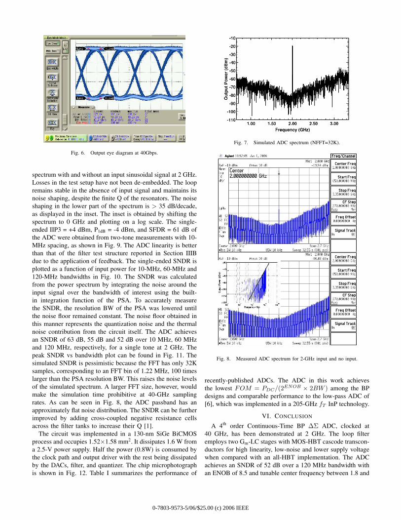
Fig. 6. Output eye diagram at 40Gbps.
spectrum with and without an input sinusoidal signal at 2 GHz.Losses in the test setup have not been de-embedded. The loopremains stable in the absence of input signal and maintains itsnoise shaping, despite the finite Q of the resonators. The noiseshaping in the lower part of the spectrum is > 35 dB/decade,as displayed in the inset. The inset is obtained by shifting thespectrum to 0 GHz and plotting on a log scale. The single-ended IIP3 = +4 dBm, P1dB = -4 dBm, and SFDR = 61 dB ofthe ADC were obtained from two-tone measurements with 10-MHz spacing, as shown in Fig. 9. The ADC linearity is betterthan that of the filter test structure reported in Section IIIBdue to the application of feedback. The single-ended SNDR isplotted as a function of input power for 10-MHz, 60-MHz and120-MHz bandwidths in Fig. 10. The SNDR was calculatedfrom the power spectrum by integrating the noise around theinput signal over the bandwidth of interest using the built-in integration function of the PSA. To accurately measurethe SNDR, the resolution BW of the PSA was lowered untilthe noise floor remained constant. The noise floor obtained inthis manner represents the quantization noise and the thermalnoise contribution from the circuit itself. The ADC achievesan SNDR of 63 dB, 55 dB and 52 dB over 10 MHz, 60 MHzand 120 MHz, respectively, for a single tone at 2 GHz. Thepeak SNDR vs bandwidth plot can be found in Fig. 11. Thesimulated SNDR is pessimistic because the FFT has only 32Ksamples, corresponding to an FFT bin of 1.22 MHz, 100 timeslarger than the PSA resolution BW. This raises the noise levelsof the simulated spectrum. A larger FFT size, however, wouldmake the simulation time prohibitive at 40-GHz samplingrates. As can be seen in Fig. 8, the ADC passband has anapproximately flat noise distribution. The SNDR can be furtherimproved by adding cross-coupled negative resistance cellsacross the filter tanks to increase their Q [1].
The circuit was implemented in a 130-nm SiGe BiCMOSprocess and occupies 1.52×1.58 mm2. It dissipates 1.6 W froma 2.5-V power supply. Half the power (0.8W) is consumed bythe clock path and output driver with the rest being dissipatedby the DACs, filter, and quantizer. The chip microphotographis shown in Fig. 12. Table I summarizes the performance of
Fig. 7. Simulated ADC spectrum (NFFT=32K).
Fig. 8. Measured ADC spectrum for 2-GHz input and no input.
recently-published ADCs. The ADC in this work achievesthe lowest FOM = PDC/(2ENOB × 2BW ) among the BPdesigns and comparable performance to the low-pass ADC of[6], which was implemented in a 205-GHz fT InP technology.
VI. CONCLUSION
A 4th order Continuous-Time BP ∆Σ ADC, clocked at40 GHz, has been demonstrated at 2 GHz. The loop filteremploys two Gm-LC stages with MOS-HBT cascode transcon-ductors for high linearity, low-noise and lower supply voltagewhen compared with an all-HBT implementation. The ADCachieves an SNDR of 52 dB over a 120 MHz bandwidth withan ENOB of 8.5 and tunable center frequency between 1.8 and
0-7803-9573-5/06/$25.00 (c) 2006 IEEE
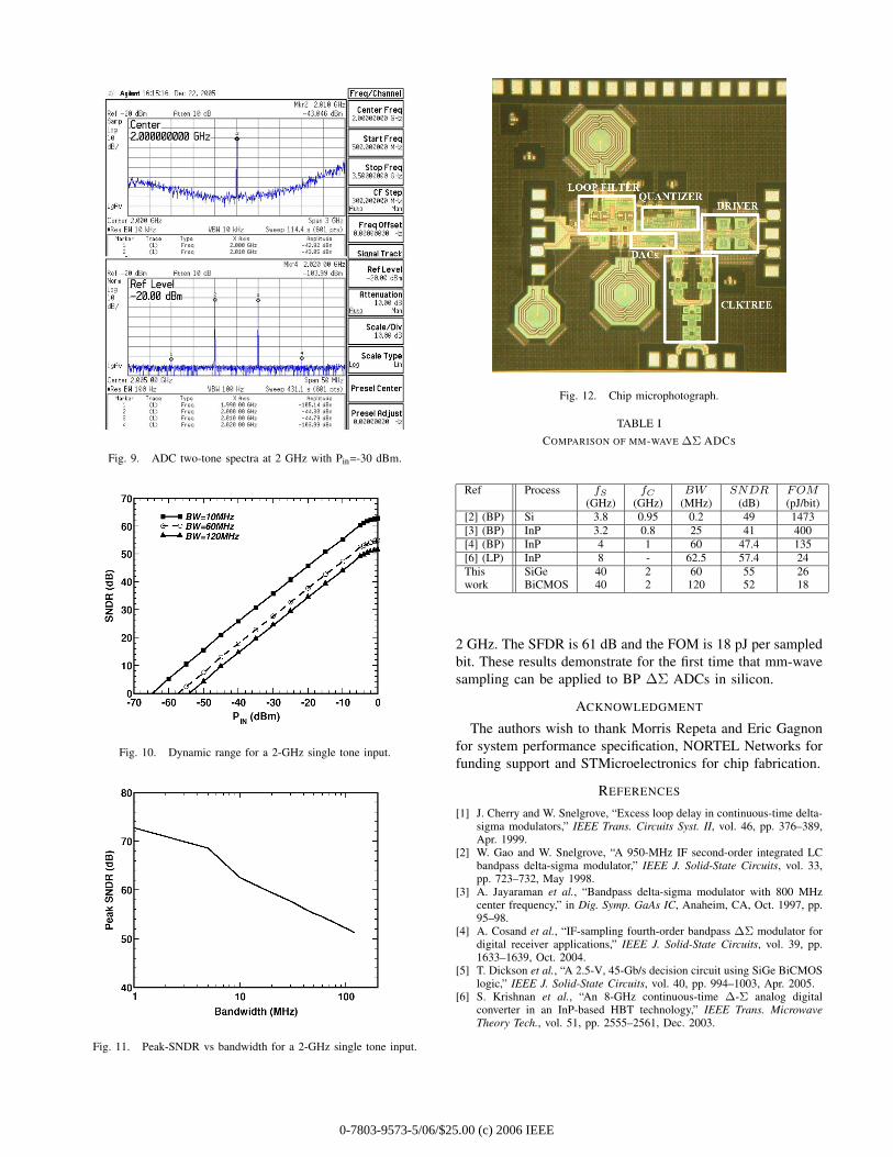
Fig. 9. ADC two-tone spectra at 2 GHz with Pin=-30 dBm.
Fig. 10. Dynamic range for a 2-GHz single tone input.
Fig. 11. Peak-SNDR vs bandwidth for a 2-GHz single tone input.
Fig. 12. Chip microphotograph.
TABLE I
COMPARISON OF MM-WAVE ∆Σ ADCS
Ref Process fS fC BW SNDR FOM(GHz) (GHz) (MHz) (dB) (pJ/bit)
[2] (BP) Si 3.8 0.95 0.2 49 1473[3] (BP) InP 3.2 0.8 25 41 400[4] (BP) InP 4 1 60 47.4 135[6] (LP) InP 8 - 62.5 57.4 24This SiGe 40 2 60 55 26work BiCMOS 40 2 120 52 18
2 GHz. The SFDR is 61 dB and the FOM is 18 pJ per sampledbit. These results demonstrate for the first time that mm-wavesampling can be applied to BP ∆Σ ADCs in silicon.
ACKNOWLEDGMENT
The authors wish to thank Morris Repeta and Eric Gagnonfor system performance specification, NORTEL Networks forfunding support and STMicroelectronics for chip fabrication.
REFERENCES
[1] J. Cherry and W. Snelgrove, “Excess loop delay in continuous-time delta-sigma modulators,” IEEE Trans. Circuits Syst. II, vol. 46, pp. 376–389,Apr. 1999.
[2] W. Gao and W. Snelgrove, “A 950-MHz IF second-order integrated LCbandpass delta-sigma modulator,” IEEE J. Solid-State Circuits, vol. 33,pp. 723–732, May 1998.
[3] A. Jayaraman et al., “Bandpass delta-sigma modulator with 800 MHzcenter frequency,” in Dig. Symp. GaAs IC, Anaheim, CA, Oct. 1997, pp.95–98.
[4] A. Cosand et al., “IF-sampling fourth-order bandpass ∆Σ modulator fordigital receiver applications,” IEEE J. Solid-State Circuits, vol. 39, pp.1633–1639, Oct. 2004.
[5] T. Dickson et al., “A 2.5-V, 45-Gb/s decision circuit using SiGe BiCMOSlogic,” IEEE J. Solid-State Circuits, vol. 40, pp. 994–1003, Apr. 2005.
[6] S. Krishnan et al., “An 8-GHz continuous-time ∆-Σ analog digitalconverter in an InP-based HBT technology,” IEEE Trans. MicrowaveTheory Tech., vol. 51, pp. 2555–2561, Dec. 2003.
0-7803-9573-5/06/$25.00 (c) 2006 IEEE


![Maximum Correntropy Criterion Kalman Filter for -Jerk ......of samples to handle non-Gaussian noises [22]. Gaussian sum filter (GSF) is an algorithm to obtain the filtering distribution](https://static.fdocument.org/doc/165x107/60a8673f2bc7e6726806176f/maximum-correntropy-criterion-kalman-filter-for-jerk-of-samples-to-handle.jpg)


![Chip-Based Lithium-Niobate Frequency Combs...comb generator [Fig. 1(a)] [12]. An electrically programmable add-drop filter is monolithically integrated to arbitrarily pick out one](https://static.fdocument.org/doc/165x107/611ad94f0b31f66c21696eb0/chip-based-lithium-niobate-frequency-combs-comb-generator-fig-1a-12.jpg)