Research Review 2002-2005 - University of Waterloo · Research Review 2002-2005 ... Natural Science...
84
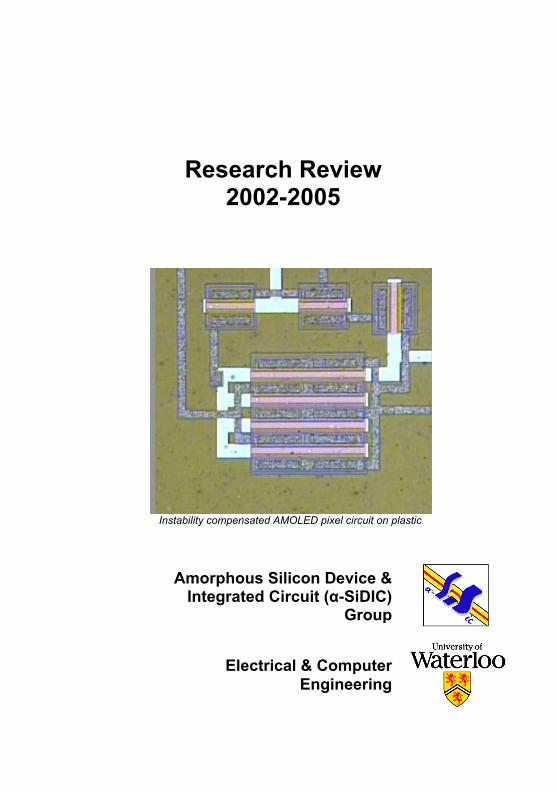
Research Review 2002-2005 Instability compensated AMOLED pixel circuit on plastic Amorphous Silicon Device & Integrated Circuit (α-SiDIC) Group Electrical & Computer Engineering
Transcript of Research Review 2002-2005 - University of Waterloo · Research Review 2002-2005 ... Natural Science...
Research Review 2002-2005
Instability compensated AMOLED pixel circuit on plastic
Amorphous Silicon Device &
Integrated Circuit (α-SiDIC) Group
Electrical & Computer Engineering
1
Amorphous Silicon Devices & Integrated Circuits (α-SiDIC)
Group
University of Waterloo Electrical & Computer Engineering
Research Review 2002 - 2005
Mailing address: Prof. Arokia Nathan
Electrical & Computer Engineering University of Waterloo Waterloo, Ontario N2L 3G1 Canada
Telephone: 519 888 4803 Fax: 519 746 6321
E-mail: [email protected]: ece.uwaterloo.ca/~a-SiDIC
2
CONTENTS Preface . . . . . . . . . . . . . . . . . . . . . . . . . . . . . . . . . . . . . . . . . . . . . . . . . 4 Sponsors . . . . . . . . . . . . . . . . . . . . . . . . . . . . . . . . . . . . . . . . . . . . . . . 5 Personnel . . . . . . . . . . . . . . . . . . . . . . . . . . . . . . . . . . . . . . . . . . . . . . . 6 1 Thin Film Transistors . . . . . . . . . . . . . . . . . . . . . . . . . . . . . . . . . . . 9
1.1 TFT Compact Modeling and Parameter Extraction 10 1.2 Highly Doped Microcrystalline Silicon for TFT Contact Layers 11 1.3 Bottom-Gate Microcrystalline Silicon TFTs 12 1.4 Top-Gate Microcrystalline Silicon TFTs 13 1.5 Nanocrystalline Silicon TFTs 14 1.6 Vertical Thin Film Transistors 15 1.7 Bias-Induced Long Term Transient in Amorphous Silicon TFTs 16 1.8 Constant Current Stress Metastability of Amorphous Silicon TFTs 17 1.9 TFT Dynamic Modeling 18
2 Flexible Electronics . . . . . . . . . . . . . . . . . . . . . . . . . . . . . . . . . . . . 19 2.1 Low Temperature Amorphous Silicon Nitride 20 2.2 Low Temprature Amorphous Silicon Oxide 21 2.3 75°C Nanocrystalline Silicon TFT 22 2.4 High Performance Amorphous Silicon TFTs on Plastic Substrates 23 2.5 Voltage- and Current-Programmed Pixel Driver Circuits on Plastic for
AMOLED Displays 24 2.6 Stability of Amorphous Silicon Pixel Driver Circuits on Polyimide Foils 25 2.7 Mechanically Strained TFTs 26 2.8 Patterning Techniques for Fabrication of Polymer Electronics 27 2.9 Organic TFT Materials and Interfaces 28 2.10 Organic TFT Architectures 29
3 Process Integration . . . . . . . . . . . . . . . . . . . . . . . . . . . . . . . . . . . . 30 3.1 Low-k Dielectrics 31 3.2 Residue Removal in CF4/H2 Plasma Etching 32 3.3 High Aspect-Ratio (AR) Photolithography 33 3.4 Thin Film Deposition on Non-Planar Topographical Surfaces 34
4 OLED Displays . . . . . . . . . . . . . . . . . . . . . . . . . . . . . . . . . . . . . . . . 35 4.1 Aacene-Anthracene Copolymers for Full Color OLED Displays 36 4.2 Synthesis of Anthracene-Naphthalene Copolymers for Green OLEDs 37 4.3 Anthracene Short Chain Copolymers for Blue OLEDs 38 4.4 Integration of Amorphous Silicon TFT and OLED for Active-Matrix
OLED Displays 39 4.5 Amorphous Silicon Demultiplexer 40 4.6 Current Programmed Pixel Circuits 41 4.7 Voltage-Programmed Feedback Pixel Circuit for OLED Displays 42 4.8 Open Loop Voltage-Programmed Pixel Circuit 43 4.9 Acceleration Factor for Circuit Testing 44 4.10 Lifetime Testing of Amorphous Silicon Pixel Circuits 45
3
4.11 Mobility Considerations for Amorphous Silicon TFT Based AMOLED Backplanes 46
5 Optical and X-Ray Imaging . . . . . . . . . . . . . . . . . . . . . . . . . . . . . . 47 5.1 Novel n-i-δi-p Photodiode 48 5.2 Two-Dimensional Photodiode Array 49 5.3 Deep-UV CCD Imaging: Degradation Mechanisms 50 5.4 Process Integration of X-Ray Direct Detection Pixel 51 5.5 Active Pixel Sensor for X-Ray Detection 52 5.6 Vertically Integrated Amorphous Silicon Active Pixels for X-Ray
Detection 53 5.7 ΔVT Compensated Amorphous Silicon Pixel Amplifier for Fluoroscopy 54 5.8 MTF Measurements of Gd2O2S:Tb Based Phosphor Films Coupled with Photodetectors 55 5.9 Digital Radiology Using Active Matrix Readout With High Voltage
Protection 56 6 Photovoltaics . . . . . . . . . . . . . . . . . . . . . . . . . . . . . . . . . . . . . . . . . 57
6.1 Low Temperature Amorphous Silicon and Nanocrystalline Silicon for Solar Cells 58
6.2 Amorphous Silicon/Multicrystalline Silicon Heterojunction Solar Cells 59 6.3 Low Temperature Solar Cells 60
Publications . . . . . . . . . . . . . . . . . . . . . . . . . . . . . . . . . . . . . . . . . . . . 61 Map . . . . . . . . . . . . . . . . . . . . . . . . . . . . . . . . . . . . . . . . . . . . . . . . . . . 83
4
Preface This report reviews the research activities of the Amorphous Silicon Devices
and Integrated Circuits (α-SiDIC) group in the period 2002-2005.
The group continues to enjoy significant growth in terms of personnel, number of projects, and laboratory infrastructure. The diversity of research projects has expanded, along with offerings of several new advanced level courses in large area electronics, ranging from electronic materials and processing to devices and integration. Major project areas include thin film transistor integration on rigid and flexible substrates, including fabrication of novel device structures, active matrix backplanes for organic light emitting diode (OLED) displays, biomedical x-ray imaging and photon counting, and photovoltaics, including flexible solar cells. Construction of the new device fabrication laboratory is now complete and installation of new state-of-the-art tools and relocation of existing equipment is currently underway.
The group has worked extremely hard over the last 2-3 year period coping with construction of the new lab, equipment installation, and new projects. We are very pleased with the outcome in terms of quality of results and intellectual property generation in a number of areas related to large area electronics. Over this period we received two best paper awards: 2002/2003 IEE Institution Premium Award for Best Paper in Devices, Circuits, and Systems (for TFT integration on glass and plastic) and the Michael B. Merickel Award in Medical Imaging 2001 (for active pixel sensors in digital fluoroscopy). A. Nathan was awarded the NSERC E.W.R. Steacie Fellowship and the Canada Research Chair in 2001 and 2004, respectively. PhD students Karim S. Karim and Peyman Servati received NSERC Doctoral Prizes in 2003 and 2004, respectively, and Anil Kumar, Flora Li, and Kapil Sakariya were awarded the 2004 CITO Research Excellence Scholarship. Anil and Kapil also received the 2004 Martin Walmsley Fellowship for Technological Entrepreneurship.
We gratefully acknowledge the support of our research sponsors and the commitment of the University towards this initiative, and look forward to the exciting times ahead! Special thanks goes to Dr. Peyman Servati and Jeff Chang who edited this Research Review.
5
Sponsors IGNIS Innovation Inc. www.ignis.ca
DALSA Inc. www.dalsa.com Eastman Kodak www.kodak.com Versentech Holdings Inc. www.versentech.com
The Westaim Corp. www.westaim.ca Regional Technology Innovation Program of the Ministry of Commerce, Industry and Energy (MOCIE) Communications Information Technology Ontario (CITO) www.cito.ca
Ontario innovation Trust (OIT) www.oit.on.ca
Natural Science and Engineering Research Council of Canada (NSERC) www.nserc.ca Canada Foundation for Innovation (CFI) www.innovation.ca University of Waterloo www.uwaterloo.ca
6
Personnel Principle Investigator Dr. Arokia Nathan, Professor Canada Research Chair, NSERC E.W.R. Steacie Fellow Dr. Andrei Sazonov, Assistant Professor Dr. Siva Sivoththaman, Associate Professor Dr. Denis Striakhilev, Research Assistant Professor Research Associates & Post-Doctoral Fellows Dr. Sarswati Koul (until Aug 05) Dr. Y. Han (until Aug 03) Dr. Raman Jeyakumar (until Aug 04) Dr. Yuriy Vygranenko Dr. Kyung-Ho Kim Dr. Mohammad Zahangir Kabir PhD Students Gholamreza Chaji Isaac Chan (until Jan 05) Jeff Chang Stella Chang Hassan El-Gohary Mohammad R. Esmaeili Rad Mahdi Farrokh Baroughi Majid Gharghi Shahin Jafarabadiash S.M. Jahinuzzaman Karim S. Karim (until Dec 02) Anil Kumar Jackson Lai Czang-Ho Lee Hyun Jung Lee Flora Li Maryam Moradi Nader Safavian Sanjiv Sambandan Peyman Servati (until Apr 04) Afrin Sultana Sheng Tao (until Dec 02) Kai Wang MASc Students Arash Akhavan Fomani (until Dec 05) Stefan Alexander (until Apr 03) Saman Asgaran (until Dec 02) Hua Bai (until Jul 04) Khadijeh Bayat Yong Cai (until Oct 04) Saeed Fathololoumi (until Dec 05) David Grant (until Dec 04) Syed Iftekhar Ali (until Sep 04) Farzad Khalvati (until Aug 03) K. Khodayariz (until Dec 02) C. McArthur (until Oct 03) Ricky Huang (until Dec 05) Kambiz K.Moez (until Dec 02) Alfredo A. Munoz (until Apr 03) Clement Ng
7
Luyang Ren (until May 02) Ye Zhou (until Dec 02) Raymond Zhu (until Dec 05) George Chuang-Tsu Chiang Visiting Professor & Visiting/Exchange Student Prof. Gin Nam (May 04 to Jan 05) Tim Boescke (Aug 02 to Nov 02) Frauke Greve (Oct 01 to Mar 02) Michael Reich (May 03 to Oct 03) Stefan Schonhardt (Dec 03 to Sep 04) Undergraduate/Co-op Students Yu Bai Ed Horne James Lin Wenqian Han Sun-Hong Wu Gerrit Ledderhof David Teplinsky Keith Chan Adam Sikka Shaaj Vijay Yu Peng Wang Samuel Chen Alex Wang Clement Ng Rick I-Heng Huang Anton Fischer Nino Zahirovic Tony Kao Sam Chen Kellen George Kieffer Pavneet Bajwa Technical Staff Stefan Alexander Robert Mullins Joseph Street (until Mar 05) Sheng Tao (until Oct 04) Richard Barber (Facility Manager)
Finance and Administration Eliza Ho
8
1 Thin Film Transistors
Cr
Cr
250 nm100 nm250 nm
50 nm
Cr
a-SiNx:Hn+ a-Si:H
n+ a-Si:H100 nm
300 nm
100 nm
300 nm
GateDrain
Channel
Source 100 nm
a-SiNx:Hi a-Si:H
a-SiNx:HCr
Cr
250 nm100 nm250 nm
50 nm
Cr
a-SiNx:Hn+ a-Si:H
n+ a-Si:H100 nm
300 nm
100 nm
300 nm
GateDrain
Channel
Source 100 nm
a-SiNx:Hi a-Si:H
a-SiNx:H
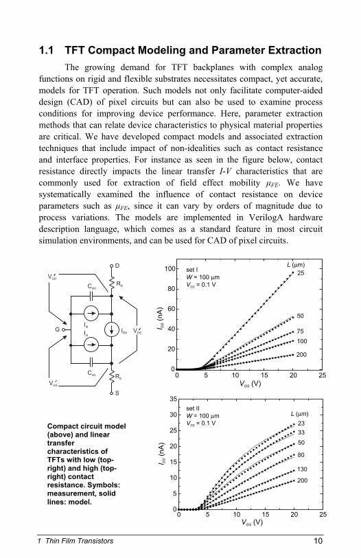
1.1 TFT Compact Modeling and Parameter Extraction The growing demand for TFT backplanes with complex analog
functions on rigid and flexible substrates necessitates compact, yet accurate, models for TFT operation. Such models not only facilitate computer-aided design (CAD) of pixel circuits but can also be used to examine process conditions for improving device performance. Here, parameter extraction methods that can relate device characteristics to physical material properties are critical. We have developed compact models and associated extraction techniques that include impact of non-idealities such as contact resistance and interface properties. For instance as seen in the figure below, contact resistance directly impacts the linear transfer I-V characteristics that are commonly used for extraction of field effect mobility μFE. We have systematically examined the influence of contact resistance on device parameters such as μFE, since it can vary by orders of magnitude due to process variations. The models are implemented in VerilogA hardware description language, which comes as a standard feature in most circuit simulation environments, and can be used for CAD of pixel circuits.
0 5 10 15 20 250
20
40
60
80
100
200
100
75
50
25
L ( m)
VGS (V)
I DS
(nA
)
set I
= 100 mW
VDS = 0.1 V
Idt
IDS
Cold
Cols
Ist
RD
RS
D
S
G VDS
VGD
VGS
L ( m)
I DS
(nA
)
0 5 10 15 20 250
5
10
15
20
25
30
35
VGS (V)
200
130
80
50
33
23
set II
= 100 mW
VDS = 0.1 V Compact circuit model (above) and linear transfer characteristics of TFTs with low (top-right) and high (top-right) contact resistance. Symbols: measurement, solid lines: model.
10
1 Thin Film Transistors
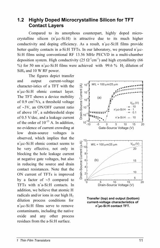
1.2 Highly Doped Microcrystalline Silicon for TFT Contact Layers Compared to its amorphous counterpart, highly doped micro-
crystalline silicon (n+μc-Si:H) is attractive due to its much higher conductivity and doping efficiency. As a result, n+μc-Si:H films provide better quality contacts in a-Si:H TFTs. In our laboratory, we prepared n+μc-Si:H films using conventional RF 13.56 MHz PECVD in a multi-chamber deposition system. High conductivity (25 Ω-1cm-1) and high crystallinity (66 %) for 50 nm n+μc-Si:H films were achieved with 99.6 % H2 dilution of SiH4 and 10 W RF power.
The figures depict transfer and output current-voltage character-istics of a TFT with the n+μc-Si:H ohmic contact layer. The TFT shows a device mobility of 0.9 cm2/Vs, a threshold voltage of ∼3V, an ON/OFF current ratio of above 107, a subthreshold slope of 0.5 V/dec, and a leakage current of the order of 10-13 A. In addition, no evidence of current crowding at low drain-source voltages is observed, which implies that the n+μc-Si:H ohmic contact seems to be very effective, not only in blocking the hole leakage current at negative gate voltages, but also in reducing the source and drain contact resistances. Note that the ON current of TFTs is improved by a factor of ∼5 compared to TFTs with n+a-Si:H contacts. In addition, we believe that atomic H radicals and/or ions in our high H2 dilution process conditions for n+μc-Si:H films serve to remove contaminants, including the native oxide and any other process residues from the a-Si:H surface.
-10 -5 0 5 10 15 2010
-15
10-13
10-11
10-9
10-7
10-5
(a)
Dra
in-S
ourc
eC
urr
ent(A
)
Gate-Source Voltage (V)
W L/ = 100 m/25 m
V (V)DS
1010.1
n c-Si:H+
10n a-Si:H+
0 5 10 15 200
2
4
6
8
10
12
(b)
Drain-Source Voltage (V)
W L/ = 100 m/25 m V (V)GS
20
Dra
in-S
ourc
eC
urr
ent(
A)
15
10
5
Transfer (top) and output (bottom) current-voltage characteristics of
n+µc-Si:H contact TFT.
11
1 Thin Film Transistors
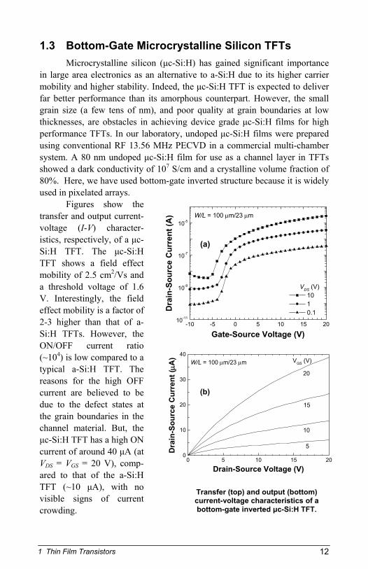
1.3 Bottom-Gate Microcrystalline Silicon TFTs Microcrystalline silicon (μc-Si:H) has gained significant importance
in large area electronics as an alternative to a-Si:H due to its higher carrier mobility and higher stability. Indeed, the μc-Si:H TFT is expected to deliver far better performance than its amorphous counterpart. However, the small grain size (a few tens of nm), and poor quality at grain boundaries at low thicknesses, are obstacles in achieving device grade μc-Si:H films for high performance TFTs. In our laboratory, undoped μc-Si:H films were prepared using conventional RF 13.56 MHz PECVD in a commercial multi-chamber system. A 80 nm undoped μc-Si:H film for use as a channel layer in TFTs showed a dark conductivity of 107 S/cm and a crystalline volume fraction of 80%. Here, we have used bottom-gate inverted structure because it is widely used in pixelated arrays.
Figures show the transfer and output current-voltage (I-V) character-istics, respectively, of a μc-Si:H TFT. The μc-Si:H TFT shows a field effect mobility of 2.5 cm2/Vs and a threshold voltage of 1.6 V. Interestingly, the field effect mobility is a factor of 2-3 higher than that of a-Si:H TFTs. However, the ON/OFF current ratio (~104) is low compared to a typical a-Si:H TFT. The reasons for the high OFF current are believed to be due to the defect states at the grain boundaries in the channel material. But, the μc-Si:H TFT has a high ON current of around 40 μA (at VDS = VGS = 20 V), comp-ared to that of the a-Si:H TFT (~10 μA), with no visible signs of current crowding.
-10 -5 0 5 10 15 2010-11
10-9
10-7
10-5
(a)
W/L = 100 μm/23 μm
VDS (V) 10 1 0.1 D
rain
-Sou
rce
Cur
rent
(A)
Gate-Source Voltage (V)
0 5 10 15 200
10
20
30
40
5
10
15
20
VGS (V)
(b)
W/L = 100 μm/23 μm
Dra
in-S
ourc
e C
urre
nt (μ
A)
Drain-Source Voltage (V)
Transfer (top) and output (bottom) current-voltage characteristics of a bottom-gate inverted μc-Si:H TFT.
12
1 Thin Film Transistors
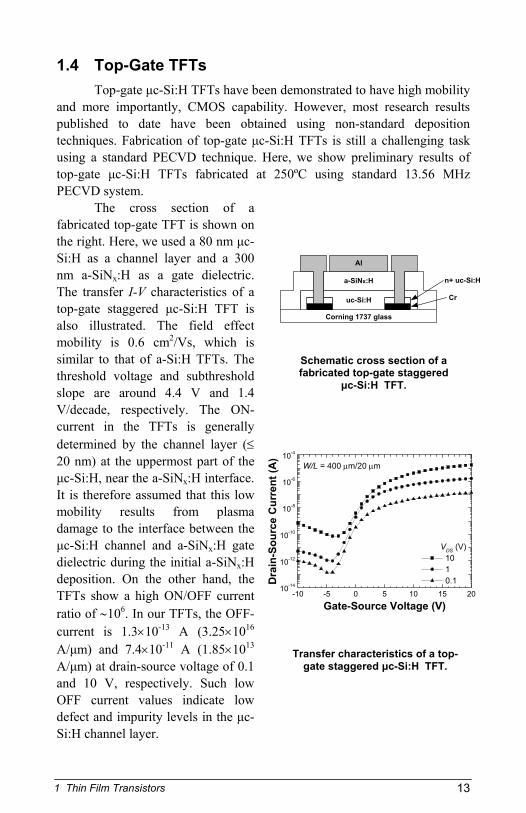
1.4 Top-Gate TFTs Top-gate μc-Si:H TFTs have been demonstrated to have high mobility
and more importantly, CMOS capability. However, most research results published to date have been obtained using non-standard deposition techniques. Fabrication of top-gate μc-Si:H TFTs is still a challenging task using a standard PECVD technique. Here, we show preliminary results of top-gate μc-Si:H TFTs fabricated at 250ºC using standard 13.56 MHz PECVD system.
The cross section of a fabricated top-gate TFT is shown on the right. Here, we used a 80 nm μc-Si:H as a channel layer and a 300 nm a-SiNx:H as a gate dielectric. The transfer I-V characteristics of a top-gate staggered μc-Si:H TFT is also illustrated. The field effect mobility is 0.6 cm2/Vs, which is similar to that of a-Si:H TFTs. The threshold voltage and subthreshold slope are around 4.4 V and 1.4 V/decade, respectively. The ON-current in the TFTs is generally determined by the channel layer (≤ 20 nm) at the uppermost part of the μc-Si:H, near the a-SiNx:H interface. It is therefore assumed that this low mobility results from plasma damage to the interface between the μc-Si:H channel and a-SiNx:H gate dielectric during the initial a-SiNx:H deposition. On the other hand, the TFTs show a high ON/OFF current ratio of ∼106. In our TFTs, the OFF-current is 1.3×10⁻¹³ A (3.25×10¹⁶ A/μm) and 7.4×10⁻¹¹ A (1.85×10¹³ A/μm) at drain-source voltage of 0.1 and 10 V, respectively. Such low OFF current values indicate low defect and impurity levels in the μc-Si:H channel layer.
Corning 1737 glass
a-SiNx:H
uc-Si:H
Al
n+ uc-Si:H
Cr
Schematic cross section of a fabricated top-gate staggered
μc-Si:H TFT.
-10 -5 0 5 10 15 2010-14
10-12
10-10
10-8
10-6
10-4
W/L = 400 μm/20 μm
VDS (V) 10 1 0.1 D
rain
-Sou
rce
Cur
rent
(A)
Gate-Source Voltage (V)
Transfer characteristics of a top-gate staggered μc-Si:H TFT.
13
1 Thin Film Transistors
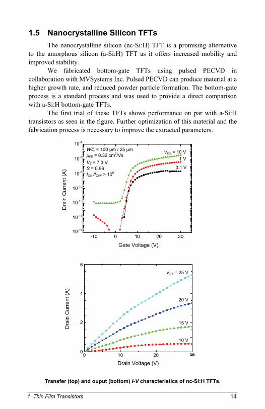
1.5 Nanocrystalline Silicon TFTs The nanocrystalline silicon (nc-Si:H) TFT is a promising alternative
to the amorphous silicon (a-Si:H) TFT as it offers increased mobility and improved stability.
We fabricated bottom-gate TFTs using pulsed PECVD in collaboration with MVSystems Inc. Pulsed PECVD can produce material at a higher growth rate, and reduced powder particle formation. The bottom-gate process is a standard process and was used to provide a direct comparison with a-Si:H bottom-gate TFTs.
The first trial of these TFTs shows performance on par with a-Si:H transistors as seen in the figure. Further optimization of this material and the fabrication process is necessary to improve the extracted parameters.
W/L = 100 μm / 25 μm μFE = 0.32 cm2/Vs VT = 7.3 V S = 0.96 ION /IOFF > 106
VDS = 10 V1 V
0.1 V
Gate Voltage (V)
Dra
in C
urre
nt (A
)
10-4
10-6
10-8
10-10
10-12
10-14
10-16
VGS = 25 V
20 V
15 V
10 V
Drain Voltage (V) 20 10 0
0
2
4
6
Dra
in C
urre
nt (A
)
Transfer (top) and ouput (bottom) I-V characteristics of nc-Si:H TFTs.
14
1 Thin Film Transistors
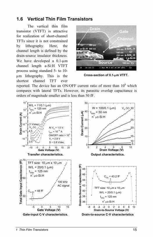
1.6 Vertical Thin Film Transistors The vertical thin film
transistor (VTFT) is attractive for realization of short-channel TFTs since it is not constrained by lithography. Here, the channel length is defined by the drain-source insulator thickness. We have developed a 0.1-μm channel length a-Si:H VTFT process using standard 5- to 10-μm lithography. This is the shortest channel TFT ever reported. The device has an ON/OFF current ratio of more than 108 which compares with lateral TFTs. However, its parasitic overlap capacitance is orders of magnitude smaller and is less than 50 fF.
Cr
Cr
250 nm100 nm250 nm
50 nm
Cr
a-SiNx:Hn+ a-Si:H
n+ a-Si:H100 nm
300 nm
100 nm
300 nm
GateDrain
Channel
Source 100 nm
a-SiNx:Hi a-Si:H
a-SiNx:HCr
Cr
250 nm100 nm250 nm
50 nm
Cr
a-SiNx:Hn+ a-Si:H
n+ a-Si:H100 nm
300 nm
100 nm
300 nm
GateDrain
Channel
Source 100 nm
a-SiNx:Hi a-Si:H
a-SiNx:H
Cross-section of 0.1-μm VTFT.
-10 -5 0 5 10 15 2010-16
10-14
10-12
10-10
10-8
10-6
10-4
n+ μc-Si:HtSiNx = 125 nm
0.5
4.5VD (V)(1 V/step)
W/L = 11/0.1 (μm)
S = 0.8 V/decVT = 2.8 VON/OFF ratio > 108IOFF = 10-15 AAt VD = 1.5 V:
Dra
in C
urre
nt (A
)
Gate Voltage (V) Transfer characteristics.
0 2 4 6 8 100
10
20
30
40
50
n+ μc-Si:HtSiNx = 50 nm
W = 100/0.1 (μm) VG (V) 30
25
20
510
15Dra
in C
urre
nt (μ
A)
Drain Voltage (V) Output characteristics.
-5 0 5 10 15
50
60
70TFT size: 10 μm x 10 μm
CG-SD = 48 fF
n+ μc-Si:HtSiNx = 125 nmW/L = 20/0.1 (μm)
100 kHzAC signal
Tota
l Gat
e In
put C
apac
itanc
e (fF
)
Gate Voltage (V) Gate-input C-V characteristics.
-8 -6 -4 -2 0 2 4 6 8 10
36
38
40
42
44
46
48
CDS = 43.2 fF
n+ μc-Si:H
tSiNx = 125 nmW/L = 20/0.1 (μm)
TFT size: 10 μm x 10 μm
Dra
in-to
-Sou
rce
Cap
acita
nce
(fF)
Drain-to-Source Voltage (V) Drain-to-source C-V characteristics
15
1 Thin Film Transistors
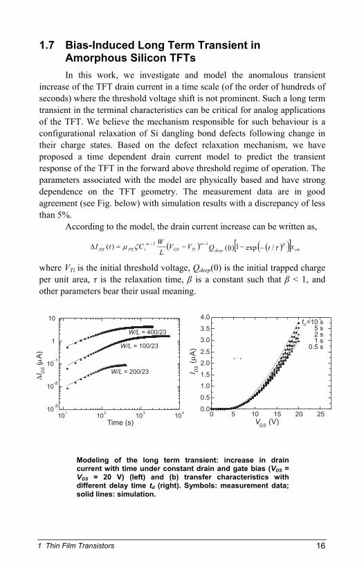
1.7 Bias-Induced Long Term Transient in Amorphous Silicon TFTs In this work, we investigate and model the anomalous transient
increase of the TFT drain current in a time scale (of the order of hundreds of seconds) where the threshold voltage shift is not prominent. Such a long term transient in the terminal characteristics can be critical for analog applications of the TFT. We believe the mechanism responsible for such behaviour is a configurational relaxation of Si dangling bond defects following change in their charge states. Based on the defect relaxation mechanism, we have proposed a time dependent drain current model to predict the transient response of the TFT in the forward above threshold regime of operation. The parameters associated with the model are physically based and have strong dependence on the TFT geometry. The measurement data are in good agreement (see Fig. below) with simulation results with a discrepancy of less than 5%.
According to the model, the drain current increase can be written as,
( ) ( )( )[ ] cmdeepTiGSiFEDS xtQVVL
WCtI βαα τζμ /exp1)0()( 12−−−=Δ −−
where VTi is the initial threshold voltage, Qdeep(0) is the initial trapped charge per unit area, τ is the relaxation time, β is a constant such that β < 1, and other parameters bear their usual meaning.
0 5 10 15 20 25
0.0
0.5
1.0
1.5
2.0
2.5
3.0
3.5
4.0
(b)
td =10 s
5 s2 s1 s
0.5 s
I DS
()
A
VGS
(V)10
110
210
310
410
-3
10-2
10-1
1
10
W/L = 200/23
W/L = 100/23
W/L = 400/23
I D
S
Time (s)
(a)
(A
)
Modeling of the long term transient: increase in drain current with time under constant drain and gate bias (VDS = VGS = 20 V) (left) and (b) transfer characteristics with different delay time td (right). Symbols: measurement data; solid lines: simulation.
16
1 Thin Film Transistors
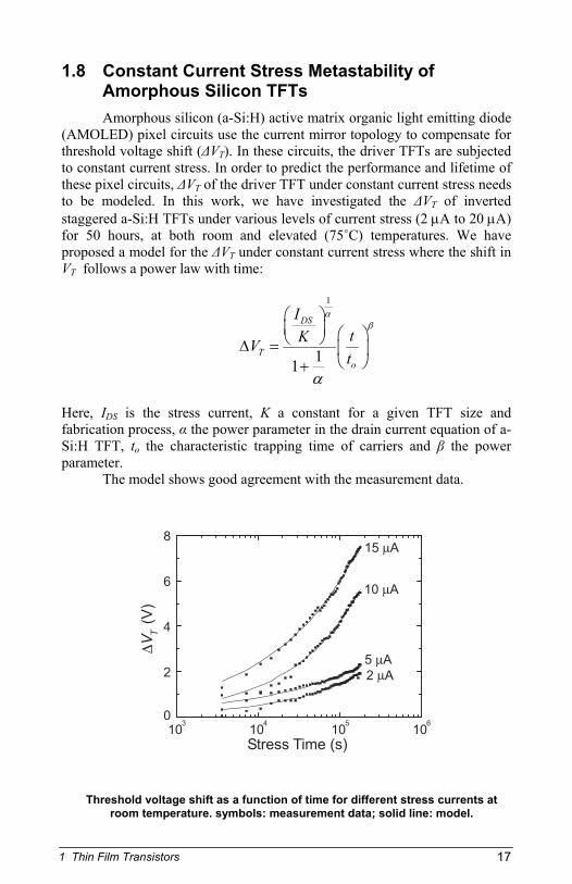
1.8 Constant Current Stress Metastability of Amorphous Silicon TFTs Amorphous silicon (a-Si:H) active matrix organic light emitting diode
(AMOLED) pixel circuits use the current mirror topology to compensate for threshold voltage shift (ΔVT). In these circuits, the driver TFTs are subjected to constant current stress. In order to predict the performance and lifetime of these pixel circuits, ΔVT of the driver TFT under constant current stress needs to be modeled. In this work, we have investigated the ΔVT of inverted staggered a-Si:H TFTs under various levels of current stress (2 μA to 20 μA) for 50 hours, at both room and elevated (75˚C) temperatures. We have proposed a model for the ΔVT under constant current stress where the shift in VT follows a power law with time:
1
11
DS
To
ItKVt
αβ
α
⎛ ⎞⎜ ⎟ ⎛ ⎞⎝ ⎠Δ = ⎜ ⎟
⎝ ⎠+
Here, IDS is the stress current, K a constant for a given TFT size and fabrication process, α the power parameter in the drain current equation of a-Si:H TFT, to the characteristic trapping time of carriers and β the power parameter.
The model shows good agreement with the measurement data.
103
104
105
106
0
2
4
6
8
2 A
5 A
10 A
15 A
V
T
Stress Time (s)
(V)
Threshold voltage shift as a function of time for different stress currents at
room temperature. symbols: measurement data; solid line: model.
17
1 Thin Film Transistors
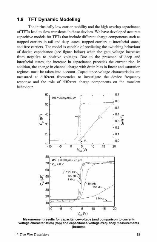
1.9 TFT Dynamic Modeling The intrinsically low carrier mobility and the high overlap capacitance
of TFTs lead to slow transients in these devices. We have developed accurate capacitive models for TFTs that include different charge components such as trapped carriers in tail and deep states, trapped carriers at interfacial states, and free carriers. The model is capable of predicting the switching behaviour of device capacitance (see figure below) when the gate voltage increases from negative to positive voltages. Due to the presence of deep and interfacial states, the increase in capacitance precedes the current rise. In addition, the change in channel charge with drain bias in linear and saturation regimes must be taken into account. Capacitance-voltage characteristics are measured at different frequencies to investigate the device frequency response and the role of different charge components on the transient behaviour.
-10 -5 0 5 10 15 2010
20
30
40
50
60
VT
W/L = 3000 m/50 m
VGS
(V)
Cgs(p
F)
0.0
0.1
0.2
0.3
0.4
0.5
0.6
0.7
IDS
(A
)
μ μ
-10 -5 0 5 10 15 20
10
20
30
40
50
60
70
80
100 kHz
1 MHz
10 kHz
f = 20 Hz
100 Hz
1 kHz
W L/ = 3000 m / 75 m
VDS
= 0 V
Cgs(p
F)
VGS
(V)
Measurement results for capacitance-voltage (and comparison to current-voltage characteristics) (top) and capacitance-voltage-frequency measurements
(bottom).
18
1 Thin Film Transistors
2 Flexible Electronics
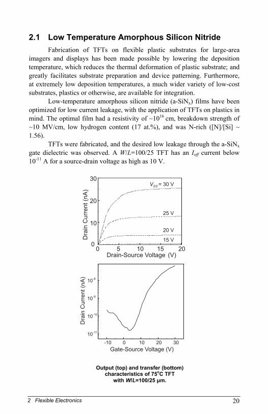
2.1 Low Temperature Amorphous Silicon Nitride Fabrication of TFTs on flexible plastic substrates for large-area
imagers and displays has been made possible by lowering the deposition temperature, which reduces the thermal deformation of plastic substrate; and greatly facilitates substrate preparation and device patterning. Furthermore, at extremely low deposition temperatures, a much wider variety of low-cost substrates, plastics or otherwise, are available for integration.
Low-temperature amorphous silicon nitride (a-SiNx) films have been optimized for low current leakage, with the application of TFTs on plastics in mind. The optimal film had a resistivity of ~1016 cm, breakdown strength of ~10 MV/cm, low hydrogen content (17 at.%), and was N-rich ([N]/[Si] ~ 1.56).
TFTs were fabricated, and the desired low leakage through the a-SiNx gate dielectric was observed. A W/L=100/25 TFT has an Ioff current below 10-11 A for a source-drain voltage as high as 10 V.
0 5 10 15 200
10
20
30
15 V
20 V
25 V
= 30 VVGS
Drain-Source Voltage (V)
Dra
inC
urr
en
t(n
A)
-10 0 10 20 30
10-11
10-10
10-9
10-8
Dra
inC
urr
ent
(nA
)
Gate-Source Voltage (V)
Output (top) and transfer (bottom) characteristics of 75oC TFT
with W/L=100/25 μm.
20
2 Flexible Electronics
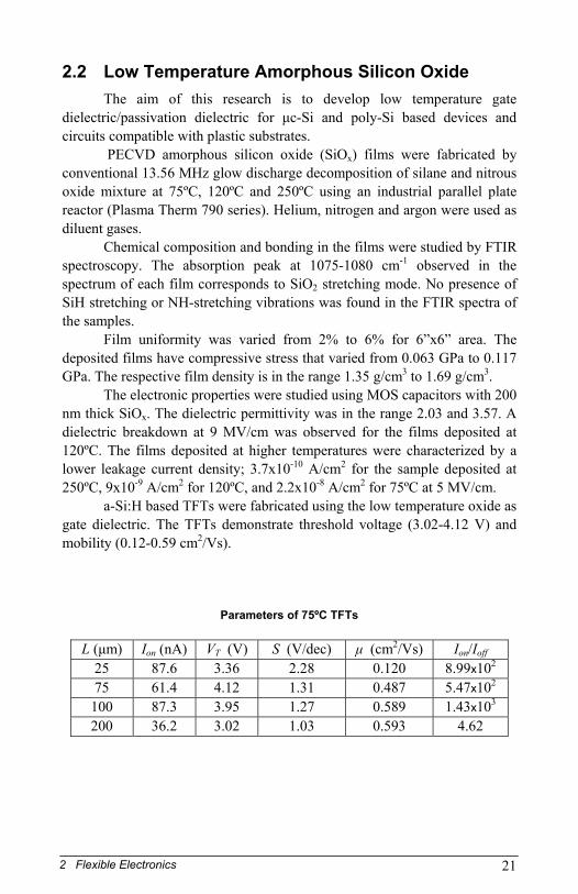
2.2 Low Temperature Amorphous Silicon Oxide The aim of this research is to develop low temperature gate
dielectric/passivation dielectric for μc-Si and poly-Si based devices and circuits compatible with plastic substrates.
PECVD amorphous silicon oxide (SiOx) films were fabricated by conventional 13.56 MHz glow discharge decomposition of silane and nitrous oxide mixture at 75ºC, 120ºC and 250ºC using an industrial parallel plate reactor (Plasma Therm 790 series). Helium, nitrogen and argon were used as diluent gases.
Chemical composition and bonding in the films were studied by FTIR spectroscopy. The absorption peak at 1075-1080 cm-1 observed in the spectrum of each film corresponds to SiO2 stretching mode. No presence of SiH stretching or NH-stretching vibrations was found in the FTIR spectra of the samples.
Film uniformity was varied from 2% to 6% for 6”x6” area. The deposited films have compressive stress that varied from 0.063 GPa to 0.117 GPa. The respective film density is in the range 1.35 g/cm3 to 1.69 g/cm3.
The electronic properties were studied using MOS capacitors with 200 nm thick SiOx. The dielectric permittivity was in the range 2.03 and 3.57. A dielectric breakdown at 9 MV/cm was observed for the films deposited at 120ºC. The films deposited at higher temperatures were characterized by a lower leakage current density; 3.7x10⁻¹⁰ A/cm2 for the sample deposited at 250ºC, 9x10⁻⁹ A/cm2 for 120ºC, and 2.2x10⁻⁸ A/cm2 for 75ºC at 5 MV/cm.
a-Si:H based TFTs were fabricated using the low temperature oxide as gate dielectric. The TFTs demonstrate threshold voltage (3.02-4.12 V) and mobility (0.12-0.59 cm2/Vs).
Parameters of 75ºC TFTs
L (μm) Ion (nA) VT (V) S (V/dec) μ (cm2/Vs) Ion/Ioff
25 87.6 3.36 2.28 0.120 8.99x10²
75 61.4 4.12 1.31 0.487 5.47x10²
100 87.3 3.95 1.27 0.589 1.43x10³
200 36.2 3.02 1.03 0.593 4.62
21
2 Flexible Electronics
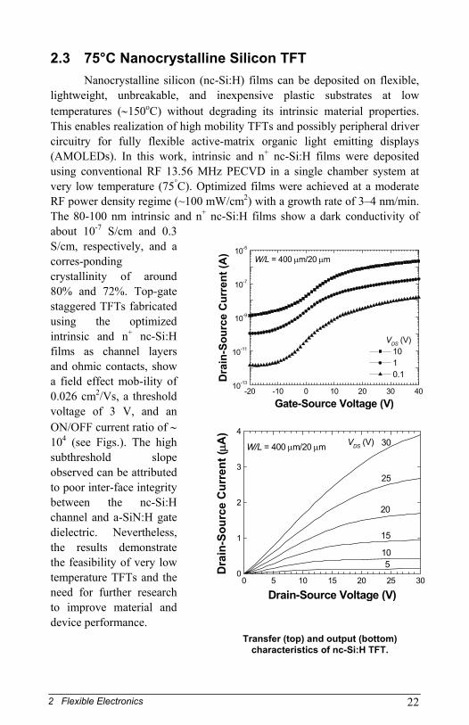
2.3 75°C Nanocrystalline Silicon TFT Nanocrystalline silicon (nc-Si:H) films can be deposited on flexible,
lightweight, unbreakable, and inexpensive plastic substrates at low temperatures (∼150oC) without degrading its intrinsic material properties. This enables realization of high mobility TFTs and possibly peripheral driver circuitry for fully flexible active-matrix organic light emitting displays (AMOLEDs). In this work, intrinsic and n+ nc-Si:H films were deposited using conventional RF 13.56 MHz PECVD in a single chamber system at very low temperature (75°C). Optimized films were achieved at a moderate RF power density regime (~100 mW/cm2) with a growth rate of 3–4 nm/min. The 80-100 nm intrinsic and n+ nc-Si:H films show a dark conductivity of about 10-7 S/cm and 0.3 S/cm, respectively, and a corres-ponding crystallinity of around 80% and 72%. Top-gate staggered TFTs fabricated using the optimized intrinsic and n+ nc-Si:H films as channel layers and ohmic contacts, show a field effect mob-ility of 0.026 cm2/Vs, a threshold voltage of 3 V, and an ON/OFF current ratio of ∼ 104 (see Figs.). The high subthreshold slope observed can be attributed to poor inter-face integrity between the nc-Si:H channel and a-SiN:H gate dielectric. Nevertheless, the results demonstrate the feasibility of very low temperature TFTs and the need for further research to improve material and device performance.
-20 -10 0 10 20 30 4010-13
10-11
10-9
10-7
10-5
W/L = 400 μm/20 μm
(a)
VDS (V) 10 1 0.1D
rain
-Sou
rce
Cur
rent
(A)
Gate-Source Voltage (V)
0 5 10 15 20 25 300
1
2
3
4
510
15
20
25
30VDS (V)
(b)
W/L = 400 μm/20 μm
Dra
in-S
ourc
e C
urre
nt (μ
A)
Drain-Source Voltage (V)
Transfer (top) and output (bottom)
characteristics of nc-Si:H TFT.
22
2 Flexible Electronics
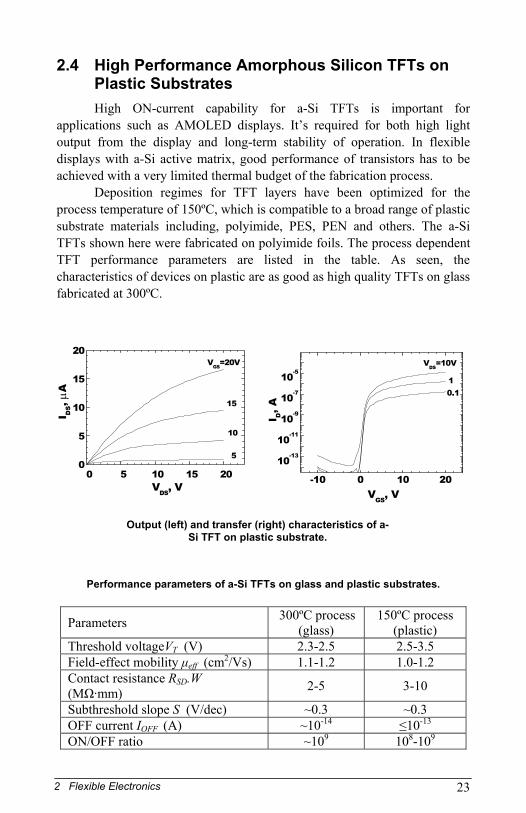
2.4 High Performance Amorphous Silicon TFTs on Plastic Substrates High ON-current capability for a-Si TFTs is important for
applications such as AMOLED displays. It’s required for both high light output from the display and long-term stability of operation. In flexible displays with a-Si active matrix, good performance of transistors has to be achieved with a very limited thermal budget of the fabrication process.
Deposition regimes for TFT layers have been optimized for the process temperature of 150ºC, which is compatible to a broad range of plastic substrate materials including, polyimide, PES, PEN and others. The a-Si TFTs shown here were fabricated on polyimide foils. The process dependent TFT performance parameters are listed in the table. As seen, the characteristics of devices on plastic are as good as high quality TFTs on glass fabricated at 300ºC.
0 5 10 15 200
5
10
15
20
a
5
10
15
VGS
=20V
I DS, μ
A
VDS
, V
-10 0 10 20
10-13
10-11
10-9
10-7
10-5 b
0.11
VDS
=10V
I D, A
VGS
, V
Output (left) and transfer (right) characteristics of a-Si TFT on plastic substrate.
Performance parameters of a-Si TFTs on glass and plastic substrates.
Parameters 300ºC process (glass)
150ºC process (plastic)
Threshold voltageVT (V) 2.3-2.5 2.5-3.5 Field-effect mobility μeff (cm2/Vs) 1.1-1.2 1.0-1.2 Contact resistance RSD.W (MΩ·mm) 2-5 3-10
Subthreshold slope S (V/dec) ~0.3 ~0.3 OFF current IOFF (A) ~10-14 ≤10-13
ON/OFF ratio ~109 108-109
23
2 Flexible Electronics
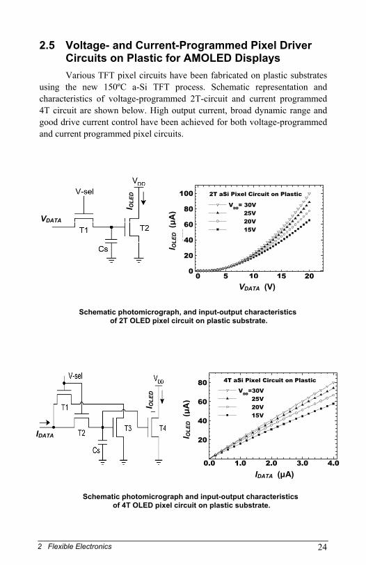
2.5 Voltage- and Current-Programmed Pixel Driver Circuits on Plastic for AMOLED Displays Various TFT pixel circuits have been fabricated on plastic substrates
using the new 150ºC a-Si TFT process. Schematic representation and characteristics of voltage-programmed 2T-circuit and current programmed 4T circuit are shown below. High output current, broad dynamic range and good drive current control have been achieved for both voltage-programmed and current programmed pixel circuits.
0 5 10 15 20
0
20
40
60
80
100 2T aSi Pixel Circuit on Plastic
b
VDD
= 30V 25V 20V 15V
I OLE
D, μ
A
I OLE
D
I OLE
D (μA
)
VDATA
VDATA
, VVDATA (V)
Schematic photomicrograph, and input-output characteristics of 2T OLED pixel circuit on plastic substrate.
0.0 1.0 2.0 3.0 4.0
20
40
60
80
b
4T aSi Pixel Circuit on Plastic
VDD
=30V 25V 20V 15V
I OLE
D, μ
A
IDATA
, μA
I OLE
D (μA
)
I OLE
D
IDATA
IDATA (μA)
Schematic photomicrograph and input-output characteristics of 4T OLED pixel circuit on plastic substrate.
24
2 Flexible Electronics
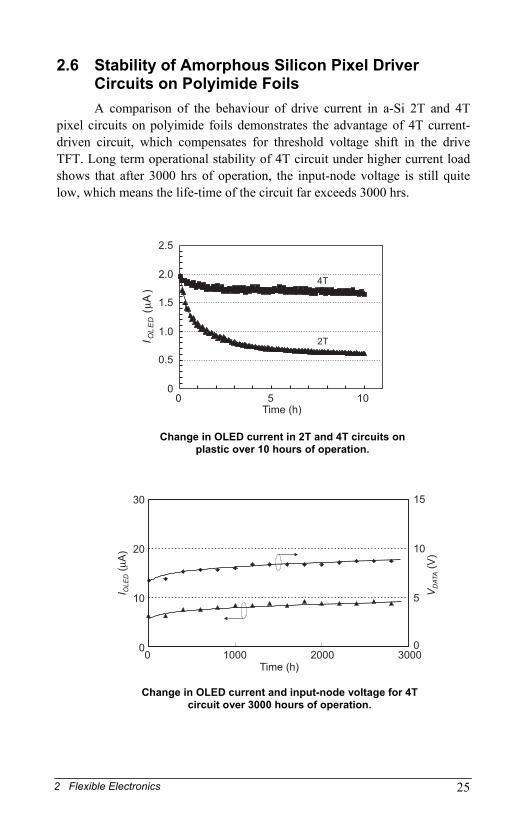
2.6 Stability of Amorphous Silicon Pixel Driver Circuits on Polyimide Foils A comparison of the behaviour of drive current in a-Si 2T and 4T
pixel circuits on polyimide foils demonstrates the advantage of 4T current-driven circuit, which compensates for threshold voltage shift in the drive TFT. Long term operational stability of 4T circuit under higher current load shows that after 3000 hrs of operation, the input-node voltage is still quite low, which means the life-time of the circuit far exceeds 3000 hrs.
0
0.5
1.0
1.5
2.0
2.5
0 5 10Time (h)
I OL
ED
(A
)
4T
2T
Change in OLED current in 2T and 4T circuits on plastic over 10 hours of operation.
0
10
20
30
0 1000 2000 3000Time (h)
0
5
10
15
I OLE
D(
A)
VD
ATA
(V)
Change in OLED current and input-node voltage for 4T
circuit over 3000 hours of operation.
25
2 Flexible Electronics
2.7 Mechanically Strained TFTs Aside from technological challenges associated with fabrication of
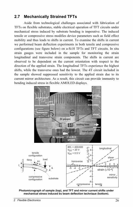
TFTs on flexible substrates, stable electrical operation of TFT circuits under mechanical stress induced by substrate bending is imperative. The induced tensile or compressive stress modifies device parameters such as field effect mobility and thus leads to shifts in current. To examine the shifts in current we performed beam deflection experiments in both tensile and compressive configurations (see figure below) on a-Si:H TFTs and TFT circuits. In situ strain gauges were included in the sample for monitoring the strain longitudinal and transverse strain components. The shifts in current are observed to be dependent on the current orientation with respect to the direction of the applied strain. The longitudinal TFTs experience the highest shifts, while the transverse ones had the lowest. The 4T circuit included in the sample showed suppressed sensitivity to the applied strain due to its current mirror architecture. As a result, this circuit can provide immunity to bending induced stress in flexible AMOLED displays.
bond pads
Al gauges
n c-Si:H
gauges
+Mo gauges
appliedstrain
TFTs
shear
transverse
longitudinal
TFTcircuits
longitudinal
transverse
routing lines
tensile
strain ( 10 )x -4
compressive
I
ID
D/
(1
0)
x-3 longitudinal
W LV
V
/ = 400/400= 20 V
= 0.5 VGS
DS
transverse
shear
-5 -4 -3
3 4 5
-6
-4
-2
2
4
6
ts
load
tensileconfiguration
compressiveconfiguration
films
substrate
12
3
mirrorsensitivity
Photomicrograph of sample (top), and TFT and mirror current shifts under mechanical stress induced by beam deflection technique (bottom).
26
2 Flexible Electronics
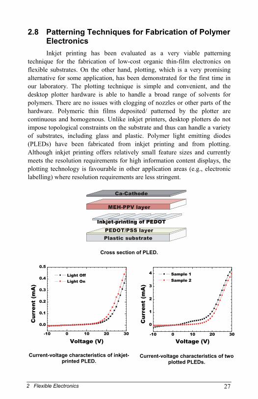
2.8 Patterning Techniques for Fabrication of Polymer Electronics Inkjet printing has been evaluated as a very viable patterning
technique for the fabrication of low-cost organic thin-film electronics on flexible substrates. On the other hand, plotting, which is a very promising alternative for some application, has been demonstrated for the first time in our laboratory. The plotting technique is simple and convenient, and the desktop plotter hardware is able to handle a broad range of solvents for polymers. There are no issues with clogging of nozzles or other parts of the hardware. Polymeric thin films deposited/ patterned by the plotter are continuous and homogenous. Unlike inkjet printers, desktop plotters do not impose topological constraints on the substrate and thus can handle a variety of substrates, including glass and plastic. Polymer light emitting diodes (PLEDs) have been fabricated from inkjet printing and from plotting. Although inkjet printing offers relatively small feature sizes and currently meets the resolution requirements for high information content displays, the plotting technology is favourable in other application areas (e.g., electronic labelling) where resolution requirements are less stringent.
Ca-Cathode
MEH-PPV layer
Inkjet-printing of PEDOT
Plastic substrate
PEDOT/PSS layerPlastic substrate
Ca-Cathode
MEH-PPV layer
Inkjet-printing of PEDOT
Plastic substrate
PEDOT/PSS layerPlastic substrate
Cross section of PLED.
-10 0 10 20 30
0.0
0.1
0.2
0.3
0.4
0.5
Cur
rent
(m
A)
Voltage (V)
Light Off Light On
Current-voltage characteristics of inkjet-printed PLED.
-10 0 10 20 30
0
1
2
3
4
Cur
rent
(m
A)
Voltage (V)
Sample 1 Sample 2
Current-voltage characteristics of two plotted PLEDs.
27
2 Flexible Electronics
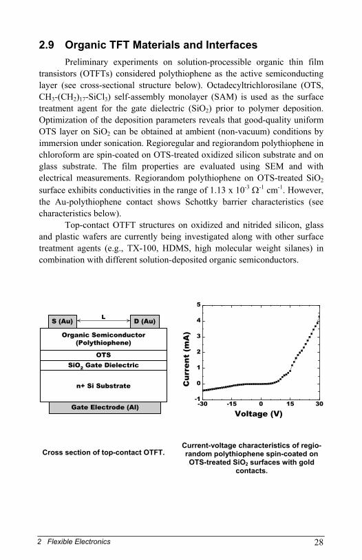
2.9 Organic TFT Materials and Interfaces Preliminary experiments on solution-processible organic thin film
transistors (OTFTs) considered polythiophene as the active semiconducting layer (see cross-sectional structure below). Octadecyltrichlorosilane (OTS, CH3-(CH2)17-SiCl3) self-assembly monolayer (SAM) is used as the surface treatment agent for the gate dielectric (SiO2) prior to polymer deposition. Optimization of the deposition parameters reveals that good-quality uniform OTS layer on SiO2 can be obtained at ambient (non-vacuum) conditions by immersion under sonication. Regioregular and regiorandom polythiophene in chloroform are spin-coated on OTS-treated oxidized silicon substrate and on glass substrate. The film properties are evaluated using SEM and with electrical measurements. Regiorandom polythiophene on OTS-treated SiO2 surface exhibits conductivities in the range of 1.13 x 10⁻³ Ω-1 cm-1. However, the Au-polythiophene contact shows Schottky barrier characteristics (see characteristics below).
Top-contact OTFT structures on oxidized and nitrided silicon, glass and plastic wafers are currently being investigated along with other surface treatment agents (e.g., TX-100, HDMS, high molecular weight silanes) in combination with different solution-deposited organic semiconductors.
S (Au) D (Au)L
n+ Si Substrate
SiO2 Gate Dielectric
Gate Electrode (Al)
Organic Semiconductor(Polythiophene)
OTS
Cross section of top-contact OTFT.
-30 -15 0 15 30-1
0
1
2
3
4
5
Cur
rent
(m
A)
Voltage (V)
Current-voltage characteristics of regio-random polythiophene spin-coated on OTS-treated SiO2 surfaces with gold
contacts.
28
2 Flexible Electronics
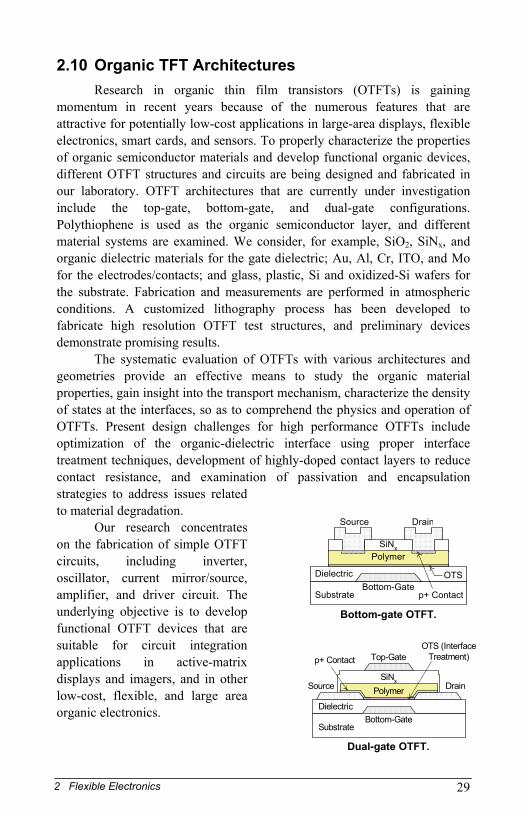
2.10 Organic TFT Architectures Research in organic thin film transistors (OTFTs) is gaining
momentum in recent years because of the numerous features that are attractive for potentially low-cost applications in large-area displays, flexible electronics, smart cards, and sensors. To properly characterize the properties of organic semiconductor materials and develop functional organic devices, different OTFT structures and circuits are being designed and fabricated in our laboratory. OTFT architectures that are currently under investigation include the top-gate, bottom-gate, and dual-gate configurations. Polythiophene is used as the organic semiconductor layer, and different material systems are examined. We consider, for example, SiO2, SiNx, and organic dielectric materials for the gate dielectric; Au, Al, Cr, ITO, and Mo for the electrodes/contacts; and glass, plastic, Si and oxidized-Si wafers for the substrate. Fabrication and measurements are performed in atmospheric conditions. A customized lithography process has been developed to fabricate high resolution OTFT test structures, and preliminary devices demonstrate promising results.
The systematic evaluation of OTFTs with various architectures and geometries provide an effective means to study the organic material properties, gain insight into the transport mechanism, characterize the density of states at the interfaces, so as to comprehend the physics and operation of OTFTs. Present design challenges for high performance OTFTs include optimization of the organic-dielectric interface using proper interface treatment techniques, development of highly-doped contact layers to reduce contact resistance, and examination of passivation and encapsulation strategies to address issues related to material degradation.
Substrate
Source Drain
Polymer
OTS
SiNx
DielectricBottom-Gate
p+ Contact
Our research concentrates on the fabrication of simple OTFT circuits, including inverter, oscillator, current mirror/source, amplifier, and driver circuit. The underlying objective is to develop functional OTFT devices that are suitable for circuit integration applications in active-matrix displays and imagers, and in other low-cost, flexible, and large area organic electronics.
Bottom-gate OTFT.
Top-Gate
Substrate
Source DrainPolymer
p+ Contact
SiNx
DielectricBottom-Gate
OTS (InterfaceTreatment)
Dual-gate OTFT.
29
2 Flexible Electronics
3 Process Integration
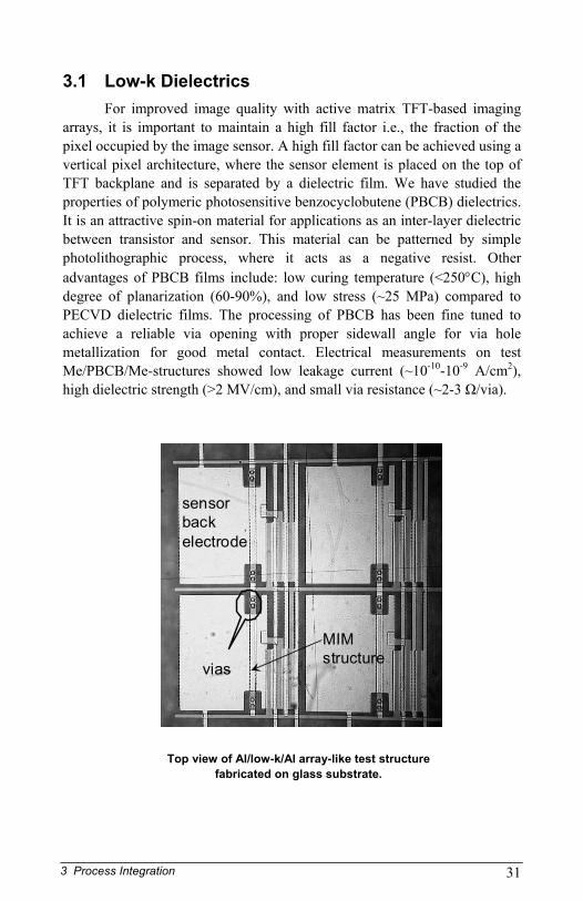
3.1 Low-k Dielectrics For improved image quality with active matrix TFT-based imaging
arrays, it is important to maintain a high fill factor i.e., the fraction of the pixel occupied by the image sensor. A high fill factor can be achieved using a vertical pixel architecture, where the sensor element is placed on the top of TFT backplane and is separated by a dielectric film. We have studied the properties of polymeric photosensitive benzocyclobutene (PBCB) dielectrics. It is an attractive spin-on material for applications as an inter-layer dielectric between transistor and sensor. This material can be patterned by simple photolithographic process, where it acts as a negative resist. Other advantages of PBCB films include: low curing temperature (<250°C), high degree of planarization (60-90%), and low stress (~25 MPa) compared to PECVD dielectric films. The processing of PBCB has been fine tuned to achieve a reliable via opening with proper sidewall angle for via hole metallization for good metal contact. Electrical measurements on test Me/PBCB/Me-structures showed low leakage current (~10-10-10-9 A/cm2), high dielectric strength (>2 MV/cm), and small via resistance (~2-3 Ω/via).
sensorbackelectrode
vias
MIMstructure
sensorbackelectrode
vias
MIMstructure
Top view of Al/low-k/Al array-like test structure fabricated on glass substrate.
31
3 Process Integration
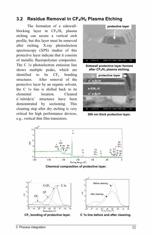
3.2 Residue Removal in CF4/H2 Plasma Etching The formation of a sidewall-
blocking layer in CF4/H2 plasma etching can secure a vertical etch profile, but this layer must be removed after etching. X-ray photoelectron spectroscopy (XPS) studies of this protective layer indicate that it consists of metallic fluoropolymer composites. The C 1s photoelectron emission line shows multiple peaks, which are identified to be CFx bonding structures. After removal of the protective layer by an organic solvent, the C 1s line is shifted back to its elemental location. Cleaned n+/nitride/n+ structures have been demonstrated by sectioning. This cleaning step after dry etching is very critical for high performance devices, e.g., vertical thin film transistors.
protective layer
Sidewall protective layer formed after CF4/H2 plasma etching.
protective layer
n+ a-Si:H
n+ a-Si:H
a-SiNx:H
Cr
500 nm thick protective layer.
Na 2p
Al 2p
Ba 4d5/2
4d3/2
Al 2sC
1s
Ca 2p3/2
2p1/2
O 1s
F 1s
Ba 3d5/2
F AES
F AES
Si 2p
Ba 3d3/2
Chemical composition of protective layer.
C 1s C-CFx
CF
CF2
CFx bonding of protective layer.
Before cleaning
After cleaning
C 1s line before and after cleaning.
32
3 Process Integration
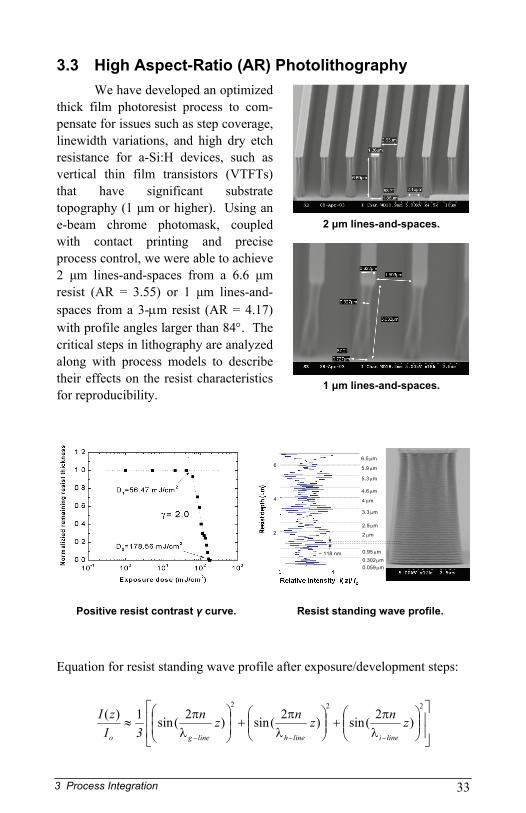
3.3 High Aspect-Ratio (AR) Photolithography We have developed an optimized
thick film photoresist process to com-pensate for issues such as step coverage, linewidth variations, and high dry etch resistance for a-Si:H devices, such as vertical thin film transistors (VTFTs) that have significant substrate topography (1 μm or higher). Using an e-beam chrome photomask, coupled with contact printing and precise process control, we were able to achieve 2 μm lines-and-spaces from a 6.6 μm resist (AR = 3.55) or 1 μm lines-and-spaces from a 3-μm resist (AR = 4.17) with profile angles larger than 84°. The critical steps in lithography are analyzed along with process models to describe their effects on the resist characteristics for reproducibility.
2 μm lines-and-spaces.
1 μm lines-and-spaces.
~ 118 nm 0.95 μm0.302μm0.059 μm
2 μm
2.5 μm
3.3 μm
4 μm
4.6 μm
5.3 μm
6.5 μm
5.9 μm
4
2
6
Positive resist contrast γ curve. Resist standing wave profile.
Equation for resist standing wave profile after exposure/development steps:
⎥⎥
⎦
⎤
⎢⎢
⎣
⎡⎟⎟⎠
⎞⎜⎜⎝
⎛λπ
+⎟⎟⎠
⎞⎜⎜⎝
⎛λπ
+⎟⎟⎠
⎞⎜⎜⎝
⎛
λπ
≈−−−
222
)2(sin)2(sin)2(sin1)( znznzn3I
zI
lineilinehlinego
33
3 Process Integration
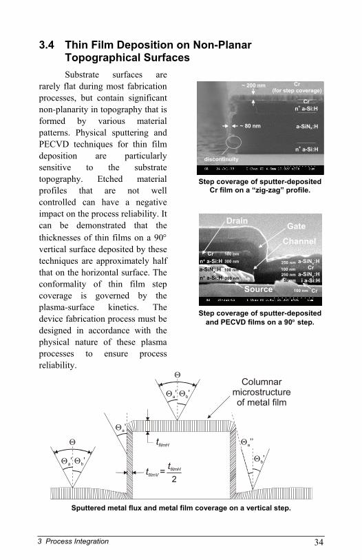
3.4 Thin Film Deposition on Non-Planar Topographical Surfaces Substrate surfaces are
rarely flat during most fabrication processes, but contain significant non-planarity in topography that is formed by various material patterns. Physical sputtering and PECVD techniques for thin film deposition are particularly sensitive to the substrate topography. Etched material profiles that are not well controlled can have a negative impact on the process reliability. It can be demonstrated that the thicknesses of thin films on a 90° vertical surface deposited by these techniques are approximately half that on the horizontal surface. The conformality of thin film step coverage is governed by the plasma-surface kinetics. The device fabrication process must be designed in accordance with the physical nature of these plasma processes to ensure process reliability.
Cr
(for step coverage)
n+ a-Si:H
a-SiNx:H
Cr
~ 200 nm
~ 80 nm
n+ a-Si:H
discontinuity
Step coverage of sputter-deposited Cr film on a “zig-zag” profile.
Cr
Cr
250 nm100 nm250 nm
50 nm
Cr
a-SiNx:Hn+ a-Si:H
n+ a-Si:H100 nm
300 nm
100 nm
300 nm
GateDrain
Channel
Source 100 nm
a-SiNx:Hi a-Si:H
a-SiNx:HCr
Cr
250 nm100 nm250 nm
50 nm
Cr
a-SiNx:Hn+ a-Si:H
n+ a-Si:H100 nm
300 nm
100 nm
300 nm
GateDrain
Channel
Source 100 nm
a-SiNx:Hi a-Si:H
a-SiNx:H
Step coverage of sputter-deposited and PECVD films on a 90° step.
Θb’Θa’
Θ
Θb’Θa’
Θ
Θb’
Θa’’
Columnarmicrostructureof metal film
tfilmH
t =filmV tfilmH
2
Θa’
Sputtered metal flux and metal film coverage on a vertical step.
34
3 Process Integration
4 OLED Displays
4.1 Aacene-Anthracene Copolymers for Full Color OLED Displays Solution processible copolymers based on acene-anthracene
comonomeric units were synthesized for color organic light emitting diode (OLED) displays. All copolymers showed high processability and resistance to aerial oxidation. The color tuning in these polymers is achieved by controlling the molar ratios of reactants to oxidant during synthesis. Structural evaluation was done by SEM. Diffraction studies reveal the presence of 40% crystalline and 60% amorphous volume fracture within the copolymeric matrix. The electroluminescence (EL) efficiency varies with the anthracene concentration present along acene structure units.
Ab
so
rba
nce
(%)
4
2
0
4
2
0
400 600 800
Wavelength (nm)
A4
A3
A6
A5
400 600 800
Inte
nsity
(a.u
.)
400 600 800
Wavelength (nm)
A1
1000
800
600
400
200
0
A2
A3
A4
Various physical properties of synthesized copolymers.
Copolymers MZ (g/mol)
MW (g/mol)
Mn (g/mol) P.D. Thermal
Stability A1 820 540 405 1.3 206ºC A2 895 415 235 1.77 210ºC A3 1150 640 390 1.64 210ºC A4 1985 655 325 2.01 392ºC A5 1005 505 300 1.68 375ºC A6 1335 505 225 2.24 210ºC
EL - spectral response of copolymers at an excitation wavelength of 418 nm.
UV-visible spectra of A3, A4, A5 and A6 copolymers in chloroform solvent.
36
4 OLED Displays
4.2 Synthesis of Anthracene-Naphthalene Copolymers for Green OLEDs A well-defined alternative technique based on statistical combination
of anthracene-naphthalene (AN) monomers for synthesis of highly soluble light emissive green copolymer was developed.
The copolymer is thermally stable up to 335ºC with complete absence of the glass transition phase. Both SEM and XRD reveal a complete amorphous nature with globular morphology. The highly processible nature eludes to the suitability of this copolymer for the fabrication of double and multilayered OLED device structures by using solution-casting techniques. A change in light emission characteristics was observed with increase in potential. The device provides green emission at 10 V, which switches to bright yellow-white emission at 13 V.
Mg:Ag 300 nm
Alq3 60 nm
AN-Copolymer 1500 rpm
ITO/Glass
Double-layer device configuration for (AN)-OLED copolymer.
Voltage (V)
800
Curr
entD
ensity
(mA
/cm
)-2
600
400
200
0
0 2 4 6 8 10 12 14 16
Exte
rnalQ
uantu
mE
ffecie
ncy
(%)
Voltage (V)
0 2 4 6 8 10 12 14 16
Current-voltage characteristics (top) and external quantum efficiency (bottom) as a function of bias voltage of (AN) double layer OLED-device.
37
4 OLED Displays
4.3 Anthracene Short Chain Copolymers for Blue OLEDs
Cathode
Electron Injection Layer
Electron Transport Layer
Emissive Layer-Blue Synthesized Copolymer
Hole Transport Layer
Hole Injection Layer
Anode – ITO/ glass (150nm)
Short-chain anthracene-polyacene based copolymer, that acts as a blue emitter for light emitting devices has been developed by using a modified Kovacic synthesis. Structurally, the copolymer exhibits an amorphous character, followed by its thermal stability up to 208ºC. An increase in electrolumin-escence efficiency was observed due to resistance over aerial oxidation. The statistical arrangement of monomeric units within the copolymeric matrix provides a keto-free defect structure. A well-defined solvatochromic behavior was observed for the copolymer.
Preliminary econsidered anthracene copoly-mer as an emissive layer for blue OLEDs. The device operates at 6 volts. Evaluation of the electrical characteristics and device parameters are in progress.
xperiments
Multilayer device structure for blue OLED.
EL-spectral response of blue gth
Solvatochromic behaviour of blue copolymer at an excitation wavelen
of 430, 480, and 560 nm. copolymer in the presence of
different solvents.
38
4 OLED Displays
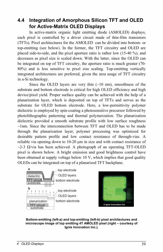
4.4 Integration of Amorphous Silicon TFT and OLED
(AMOLED) displays, each p
ED layers are very thin (~10 nm), smoothness of the substra
for Active-Matrix OLED Displays In active-matrix organic light emitting diode ixel is controlled by a driver circuit made of thin-film transistors
(TFTs). Pixel architectures for the AMOLED can be divided into bottom- or top-emitting (see below). In the former, the TFT circuitry and OLED are placed side-to-side, and the pixel aperture ratio is rather low (15-40 %), and decreases as pixel size is scaled down. With the latter, since the OLED can be integrated on top of TFT circuitry, the aperture ratio is much greater (70-80%) and is less sensitive to pixel size scaling. Top-emitting vertically integrated architectures are preferred, given the area usage of TFT circuitry in a-Si technology.
Since the OLte and bottom electrode is critical for high OLED efficiency and high
device/pixel yield. Proper surface quality can be achieved with the help of a planarization layer, which is deposited on top of TFTs and serves as the substrate for OLED bottom electrode. Here, a low-permittivity polymer dielectric is employed by spin-coating a photosensitive precursor followed by photolithographic patterning and thermal polymerzation. The planarization dielectric provided a smooth substrate profile with low surface roughness ~1nm. Since the interconnection between TFT and OLED has to be made through the planarization layer, polymer processing was optimized for desirable pattern profile and low contact resistance of through-vias. A reliable via opening down to 10-20 μm in size and with contact resistance of ~2-3 Ω/via has been achieved. A photograph of an operating TFT-OLED pixel is shown below. A bright emission and good brightness control have been obtained at supply voltage below 10 V, which implies that good quality OLEDs can be integrated on top of a planarized TFT backplane.
a
b
substrate
substrate
TFT circuit
TFT circuit
planarization
bottom electrode
OLED layers
top electrode
dielectric
bottom electrode
OLED layers
top electrode
Bottom-emitting (left-a) and top-em ing (left-b) pixel architectures and
© Ignis Innovation Inc.
itt
microscope image of top emitting 4T AMOLED pixel (right – courtesy of Ignis Innovation Inc.).
39
4 OLED Displays
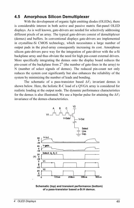
4.5 Amorphous Silicon De er odes (OLEDs), there
is con
nvariant demux is shown
multiplexWith the development of organic light emitting di
siderable interest in both active and passive matrix flat-panel OLED displays. As is well known, gate-drivers are needed for selectively addressing different pixels of an array. The typical gate-drivers consist of demultiplexer (demux) and buffers. In conventional displays gate-drivers are implemented in crystalline-Si CMOS technology, which necessitates a large number of output pads in the pixel-array consequently increasing its cost. Amorphous silicon gate-drivers pave way for the integration of gate-driver with the a-Si backplane array and thus obviate the need for high pin-count external drivers. More specifically integrating the demux onto the display board reduces the pin-count of the backplane from 2N (the number of gate-lines in the array) to N (number of select signals of demux). The reduced pin-count not only reduces the system cost significantly but also enhances the reliability of the system by minimizing the number of leads and bonding.
The schematic of a pass-transistor based ΔVT i below. Here, the holistic R-C load of a QVGA array is considered for
realistic loading at the output node. The dynamic performance characteristics for the demux is also illustrated. We use a bipolar pulse for attaining the ΔVT invariance of the demux-characteristics.
Schematic (top) and transient performance (bottom) of a pass-transistor based a-Si:H demux.
40
4 OLED Displays
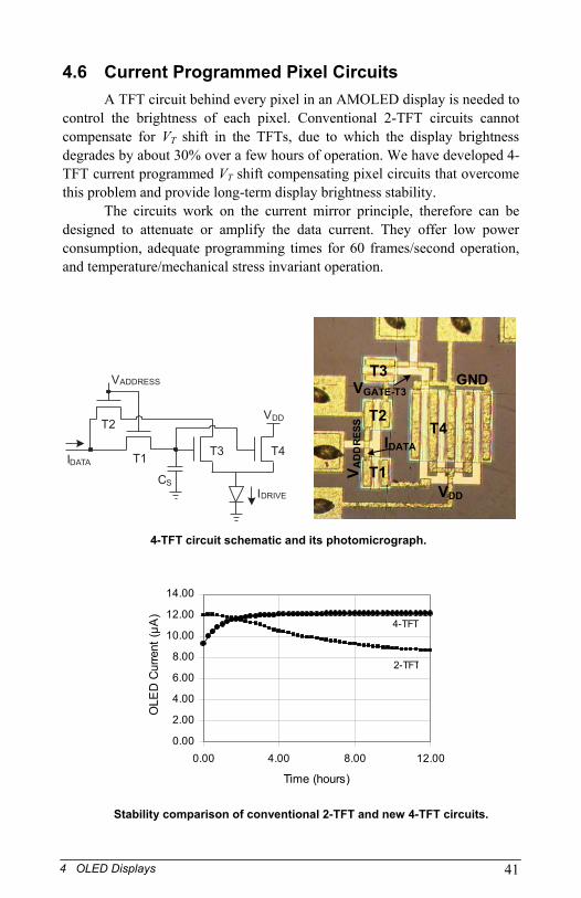
4.6 Current Programmed Pixel Circuits A TFT circuit behind every pixel in an AMOLED display is needed to
control the brightness of each pixel. Conventional 2-TFT circuits cannot compensate for VT shift in the TFTs, due to which the display brightness degrades by about 30% over a few hours of operation. We have developed 4-TFT current programmed VT shift compensating pixel circuits that overcome this problem and provide long-term display brightness stability.
The circuits work on the current mirror principle, therefore can be designed to attenuate or amplify the data current. They offer low power consumption, adequate programming times for 60 frames/second operation, and temperature/mechanical stress invariant operation.
T4T3
T2
IDRIVE
VDD
CS
IDATA
VADDRESS
T1
VDD
V AD
DR
ESS
IDATA
VGATE-T3GND
T1
T2
T3
T4
OLED Current Stability Comparison
0.00
2.00
4.00
6.00
8.00
10.00
12.00
14.00
0.00 4.00 8.00 12.00
Time (hours)
OLE
D C
urre
nt (μ
A)
4-TFT
2-TFT
4-TFT circuit schematic and its photomicrograph.
Stability comparison of conventional 2-TFT and new 4-TFT circuits.
41
4 OLED Displays
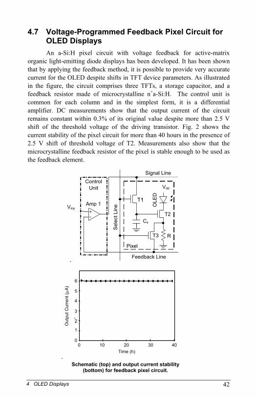
4.7 Voltage-Programmed Feedback Pixel Circuit for OLED Displays An a-Si:H pixel circuit with voltage feedback for active-matrix
organic light-emitting diode displays has been developed. It has been shown that by applying the feedback method, it is possible to provide very accurate current for the OLED despite shifts in TFT device parameters. As illustrated in the figure, the circuit comprises three TFTs, a storage capacitor, and a feedback resistor made of microcrystalline n+a-Si:H. The control unit is common for each column and in the simplest form, it is a differential amplifier. DC measurements show that the output current of the circuit remains constant within 0.3% of its original value despite more than 2.5 V shift of the threshold voltage of the driving transistor. Fig. 2 shows the current stability of the pixel circuit for more than 40 hours in the presence of 2.5 V shift of threshold voltage of T2. Measurements also show that the microcrystalline feedback resistor of the pixel is stable enough to be used as the feedback element.
Sel
ect L
ine
Feedback Line
Pixel
Amp 1Vinp
Cs
R
Vdd
T2
T3
Signal Line Control
Unit
OLE
D
Time (h) 40 30 20 10 0
0
1
2
3
4
5
6
Out
put C
urre
nt (μ
A)
Schematic (top) and output current stability (bottom) for feedback pixel circuit.
42
4 OLED Displays
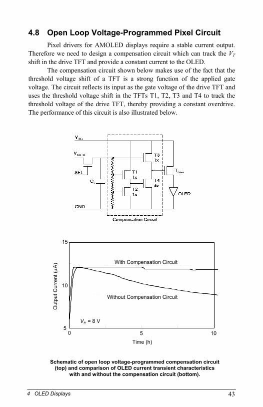
4.8 Open Loop Voltage-Programmed Pixel Circuit Pixel drivers for AMOLED displays require a stable current output.
Therefore we need to design a compensation circuit which can track the VT shift in the drive TFT and provide a constant current to the OLED.
The compensation circuit shown below makes use of the fact that the threshold voltage shift of a TFT is a strong function of the applied gate voltage. The circuit reflects its input as the gate voltage of the drive TFT and uses the threshold voltage shift in the TFTs T1, T2, T3 and T4 to track the threshold voltage of the drive TFT, thereby providing a constant overdrive. The performance of this circuit is also illustrated below.
5
10
15
0 5Time (hour)
OLE
D c
u
10
rent
(μ A
)r
Without compensation circuit
With compensation circuit
Vin = 8V
Time (h)
Schematic of open loop voltage-programmed compensation circuit (top) and comparison of OLED current transient characteristics
with and without the compensation circuit (bottom).
5
Out
put C
urre
nt (μ
A)
10
15
0
With Compensation Circuit
Without Compensation Circuit
Vin = 8 V
5 10
43
4 OLED Displays
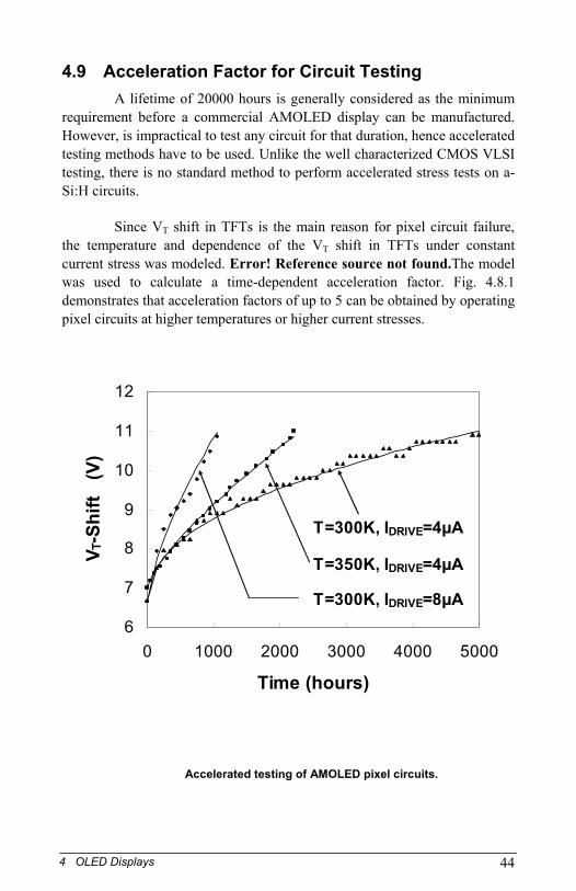
4.9 Acceleration Factor for Circuit Testing A lifetime of 20000 hours is generally considered as the minimum
requirement before a commercial AMOLED display can be manufactured. However, is impractical to test any circuit for that duration, hence accelerated testing methods have to be used. Unlike the well characterized CMOS VLSI testing, there is no standard method to perform accelerated stress tests on a-Si:H circuits.
Since VT shift in TFTs is the main reason for pixel circuit failure, the temperature and dependence of the VT shift in TFTs under constant current stress was modeled. Error! Reference source not found.The model was used to calculate a time-dependent acceleration factor. Fig. 4.8.1 demonstrates that acceleration factors of up to 5 can be obtained by operating pixel circuits at higher temperatures or higher current stresses.
6
7
8
9
10
11
12
0 1000 2000 3000 4000 5000
Time (hours)
V T-S
hift
(V)
T=300K, IDRIVE=4µA
T=350K, IDRIVE=4µA
T=300K, IDRIVE=8µA
Accelerated testing of AMOLED pixel circuits.
44
4 OLED Displays
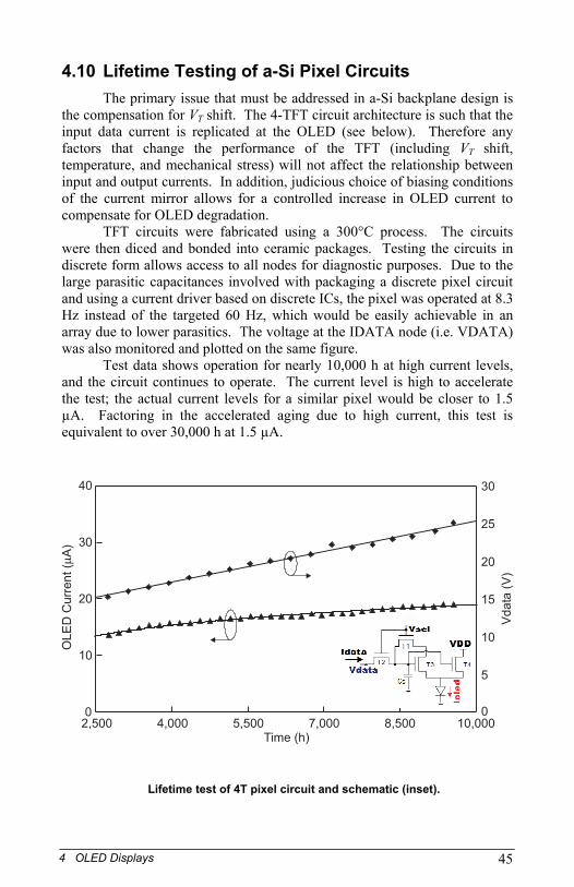
4.10 Lifetime Testing of a-Si Pixel Circuits The primary issue that must be addressed in a-Si backplane design is
the compensation for VT shift. The 4-TFT circuit architecture is such that the input data current is replicated at the OLED (see below). Therefore any factors that change the performance of the TFT (including VT shift, temperature, and mechanical stress) will not affect the relationship between input and output currents. In addition, judicious choice of biasing conditions of the current mirror allows for a controlled increase in OLED current to compensate for OLED degradation.
TFT circuits were fabricated using a 300°C process. The circuits were then diced and bonded into ceramic packages. Testing the circuits in discrete form allows access to all nodes for diagnostic purposes. Due to the large parasitic capacitances involved with packaging a discrete pixel circuit and using a current driver based on discrete ICs, the pixel was operated at 8.3 Hz instead of the targeted 60 Hz, which would be easily achievable in an array due to lower parasitics. The voltage at the IDATA node (i.e. VDATA) was also monitored and plotted on the same figure.
Test data shows operation for nearly 10,000 h at high current levels, and the circuit continues to operate. The current level is high to accelerate the test; the actual current levels for a similar pixel would be closer to 1.5 µA. Factoring in the accelerated aging due to high current, this test is equivalent to over 30,000 h at 1.5 µA.
0
10
20
30
40
2,500 4,000 5,500 7,000 8,500 10,000Time (h)
0
5
10
15
20
25
30
OL
ED
Cu
rre
nt
(A
)
Vd
ata
(V)
Lifetime test of 4T pixel circuit and schematic (inset).
45
4 OLED Displays
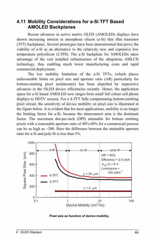
4.11 Mobility Considerations for a-Si TFT Based AMOLED Backplanes Recent advances in active matrix OLED (AMOLED) displays have
shown increasing interest in amorphous silicon (a-Si) thin film transistor (TFT) backplanes. Several prototypes have been demonstrated that prove the viability of a-Si as an alternative to the relatively new and expensive low temperature polysilicon (LTPS). The a-Si backplane for AMOLEDs takes advantage of the vast installed infrastructure of the ubiquitous AMLCD technology, thus enabling much lower manufacturing costs and rapid commercial deployment.
The low mobility limitation of the a-Si TFTs, (which places unfavourable limits on pixel size and aperture ratio (AR) particularly for bottom-emitting pixel architecture) has been dispelled by impressive advances in the OLED device efficiencies recently. Hence, the application space for a-Si based AMOLED now ranges from small full colour cell phone displays to HDTV screens. For a 4-TFT fully compensating bottom-emitting pixel circuit, the sensitivity of device mobility on pixel size is illustrated in the figure below. It is evident that for most applications, mobility is no longer the limiting factor for a-Si, because the interconnect area is the dominant factor. The maximum dot-per-inch (DPI) attainable for bottom emitting pixels with a reasonable aperture ratio of 40%-60% for a commercial process can be as high as ~200. Here the difference between the attainable aperture ratio for a-Si and poly-Si is less than 5%.
0
200
400
600
800
1000
0.1 1 10 100
Device Mobility (cm /Vs)2
Sq
ua
reP
ixe
lS
ize
(m
)
L = 25 m4-TFT
2-TFT
a-Si poly-Sinc-Si
AR = 40%
Efficiency = 2.5 cd/A
V VGS T- = 6 V
Luminance =
100 cd/m2
L = 5 m
Pixel size as function of device mobility.
46
4 OLED Displays
5 Optical and X-Ray Imaging
Glass substrate
Photodiode Switchingdiode
Mo a-Si:H ITO AlSiN Cr
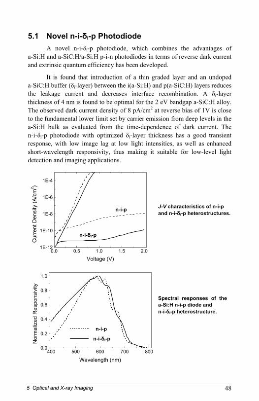
5.1 Novel n-i-δi-p Photodiode A novel n-i-δi-p photodiode, which combines the advantages of
a-Si:H and a-SiC:H/a-Si:H p-i-n photodiodes in terms of reverse dark current and extrinsic quantum efficiency has been developed.
It is found that introduction of a thin graded layer and an undoped a-SiC:H buffer (δi-layer) between the i(a-Si:H) and p(a-SiC:H) layers reduces the leakage current and decreases interface recombination. A δi-layer thickness of 4 nm is found to be optimal for the 2 eV bandgap a-SiC:H alloy. The observed dark current density of 8 pA/cm2 at reverse bias of 1V is close to the fundamental lower limit set by carrier emission from deep levels in the a-Si:H bulk as evaluated from the time-dependence of dark current. The n-i-δi-p photodiode with optimized δi-layer thickness has a good transient response, with low image lag at low light intensities, as well as enhanced short-wavelength responsivity, thus making it suitable for low-level light detection and imaging applications.
0.0 0.5 1.0 1.5 2.01E-12
1E-10
1E-8
1E-6
1E-4
n-i-δi-p
n-i-p
Cur
rent
Den
sity
(A/c
m2 )
Voltage (V)
J-V characteristics of n-i-p and n-i-δi-p heterostructures.
n-i-p
n-i-δi-p
400 500 600 700 8000.0
0.2
0.4
0.6
0.8
1.0
n-i-δi-p n-i-pN
orm
aliz
ed R
espo
nsiv
ity
Wavelength (nm)
Spectral responses of the a-Si:H n-i-p diode and n-i-δi-p heterostructure.
n-i-p
n-i-δi-p
48
5 Optical and X-ray Imaging
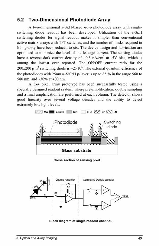
5.2 Two-Dimensional Photodiode Array A two-dimensional a-Si:H-based n-i-p photodiode array with single-
switching diode readout has been developed. Utilization of the a-Si:H switching diodes for signal readout makes it simpler than conventional active-matrix-arrays with TFT switches, and the number of masks required in lithography have been reduced to six. The device design and fabrication are optimized to minimize the level of the leakage current. The sensing diodes have a reverse dark current density of ~0.5 nA/cm2 at -5V bias, which is among the lowest ever reported. The ON/OFF current ratio for the 200x200 μm2 switching diode is ~2×10⁶. The external quantum efficiency of the photodiodes with 25nm a–SiC:H p-layer is up to 85 % in the range 560 to 580 nm, and ~30% at 400 nm.
A 3x4 pixel array prototype has been successfully tested using a specially designed readout system, where pre-amplification, double sampling and a final amplification are performed at each column. The detector shows good linearity over several voltage decades and the ability to detect extremely low light levels.
Glass substrate
Photodiode Switchingdiode
Mo a-Si:H ITO AlSiN Cr
Cross section of sensing pixel.
PD
H 1
H 2
CintIin
SD
DATA
Charge Amplifier Correlated Double sampler
G=1
G=1
G=10Vout
S1
S2
Block diagram of single readout channel.
49
5 Optical and X-ray Imaging
5.3 Deep-UV CCD Imaging: Degradation Mechanisms With an increasing number of industrial applications shifting to
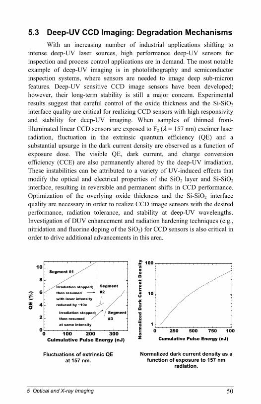
intense deep-UV laser sources, high performance deep-UV sensors for inspection and process control applications are in demand. The most notable example of deep-UV imaging is in photolithography and semiconductor inspection systems, where sensors are needed to image deep sub-micron features. Deep-UV sensitive CCD image sensors have been developed; however, their long-term stability is still a major concern. Experimental results suggest that careful control of the oxide thickness and the Si-SiO2 interface quality are critical for realizing CCD sensors with high responsivity and stability for deep-UV imaging. When samples of thinned front-illuminated linear CCD sensors are exposed to F2 (λ = 157 nm) excimer laser radiation, fluctuation in the extrinsic quantum efficiency (QE) and a substantial upsurge in the dark current density are observed as a function of exposure dose. The visible QE, dark current, and charge conversion efficiency (CCE) are also permanently altered by the deep-UV irradiation. These instabilities can be attributed to a variety of UV-induced effects that modify the optical and electrical properties of the SiO2 layer and Si-SiO2 interface, resulting in reversible and permanent shifts in CCD performance. Optimization of the overlying oxide thickness and the Si-SiO2 interface quality are necessary in order to realize CCD image sensors with the desired performance, radiation tolerance, and stability at deep-UV wavelengths. Investigation of DUV enhancement and radiation hardening techniques (e.g., nitridation and fluorine doping of the SiO2) for CCD sensors is also critical in order to drive additional advancements in this area.
0 100 200 3000
2
4
6
8
10
Segment#3
Segment#2
Irradiation stopped; then resumed at same intensity
QE
(%
)
Culmulative Pulse Energy (nJ)
Irradiation stopped; then resumed with laser intensity reduced by ~10x
Segment #1
Fluctuations of extrinsic QE at 157 nm.
0 250 500 750 1001
10
100
Nor
mal
ized
Dar
k C
urre
nt D
ensi
ty
Cumulative Pulse Energy (nJ) Normalized dark current density as a
function of exposure to 157 nm radiation.
50
5 Optical and X-ray Imaging
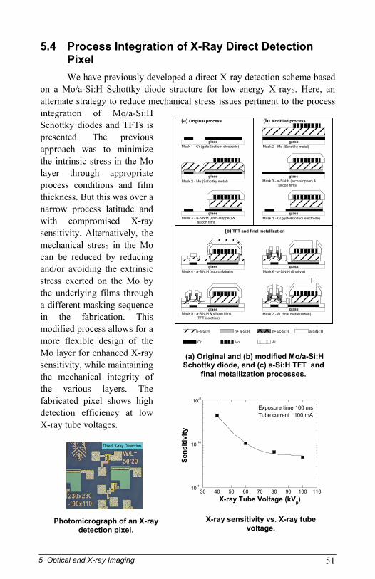
5.4 Process Integration of X-Ray Direct Detection Pixel We have previously developed a direct X-ray detection scheme based
on a Mo/a-Si:H Schottky diode structure for low-energy X-rays. Here, an alternate strategy to reduce mechanical stress issues pertinent to the process integration of Mo/a-Si:H Schottky diodes and TFTs is presented. The previous approach was to minimize the intrinsic stress in the Mo layer through appropriate process conditions and film thickness. But this was over a narrow process latitude and with compromised X-ray sensitivity. Alternatively, the mechanical stress in the Mo can be reduced by reducing and/or avoiding the extrinsic stress exerted on the Mo by the underlying films through a different masking sequence in the fabrication. This modified process allows for a more flexible design of the Mo layer for enhanced X-ray sensitivity, while maintaining the mechanical integrity of the various layers. The fabricated pixel shows high detection efficiency at low X-ray tube voltages.
i-a-Si:H n+ a-Si:H n+ uc-Si:H a-SiNx:H
Cr Mo Al
glassMask 1 - Cr (gate&bottom electrode)
glassMask 2 - Mo (Schottky metal)
Mask 3 - a-SiN:H (etch-stopper) & silicon films
glass
glassMask 5 - a-SiN:H & silicon films (TFT isolation)
Mask 6 - a-SiN:H (final via)glass
glassMask 7 - Al (final metallization)
Mask 4 - a-SiN:H (source&drain)glass
glassMask 1 - Cr (gate&bottom electrode)
Mask 2 - Mo (Schottky metal)glass
Mask 3 - a-SiN:H (etch-stopper) & silicon films
glass
(a) Original process (b) Modified process
(c) TFT and final metallization
(a) Original and (b) modified Mo/a-Si:H Schottky diode, and (c) a-Si:H TFT and
final metallization processes.
30 40 50 60 70 80 90 100 11010-11
10-10
10-9
Exposure time 100 ms Tube current 100 mA
Sens
itivi
ty
X-ray Tube Voltage (kVp)
Direct X-ray Detection
X-ray sen ivity vs. X-ray tube
sitPhot ray detection pixel.
omicrograph of an X-voltage.
51
5 Optical and X-ray Imaging
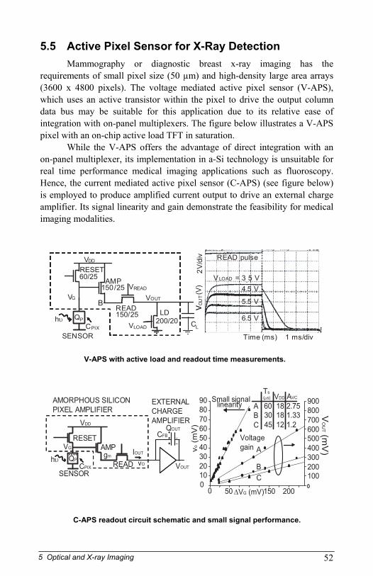
5.5 Active Pixel Sensor for X-Ray Detection Mammography or diagnostic breast x-ray imaging has the
requirements of small pixel size (50 µm) and high-density large area arrays (3600 x 4800 pixels). The voltage mediated active pixel sensor (V-APS), which uses an active transistor within the pixel to drive the output column data bus may be suitable for this application due to its relative ease of integration with on-panel multiplexers. The figure below illustrates a V-APS pixel with an on-chip active load TFT in saturation.
While the V-APS offers the advantage of direct integration with an on-panel multiplexer, its implementation in a-Si technology is unsuitable for real time performance medical imaging applications such as fluoroscopy. Hence, the current mediated active pixel sensor (C-APS) (see figure below) is employed to produce amplified current output to drive an external charge amplifier. Its signal linearity and gain demonstrate the feasibility for medical imaging modalities.
hυ
AMP150/25
READ
200/20
B
CLCPIX
SENSOR
QP
VOUT
VREAD
150/25
60/25
VG
VDD
VLOAD
LD
READ pulse
V LOAD
= 3.5 V
4.5 V
6.5 V5.5 VV O
UT
READ pulse
VLOAD = 3.5 V4.5 V
6.5 V
5.5 V
V(V
)
Time (ms) 1 ms/div
2V/d
iv
RESET
V-APS with active load and readout time measurements.
+++
__
+ + + +
EXTERNAL CHARGE AMPLIFIER
+++ _
VDD
SENSOR
AMP
AMORPHOUS SILICON PIXEL AMPLIFIER
hυ QP+ + + +
CPIX
00102030405060708090
0 50ΔVG (mV)150 2000
100200300400500600700800900
vo (m
V)
VO
UT (m
V)
Small signallinearity
Voltagegain
VDD
60 18 2.7530 18 1.3345 12 1.2
ABC
A
BC
VG
RESET
gm
READ
IOUT
vO
CFBQOUT
VOUT
AVCTs (μs)
C-APS readout circuit schematic and small signal performance.
52
5 Optical and X-ray Imaging
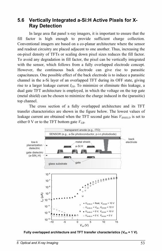
5.6 Vertically Integrated a-Si:H Active Pixels for X-Ray Detection In large area flat panel x-ray imagers, it is important to ensure that the
fill factor is high enough to provide sufficient charge collection. Conventional imagers are based on a co-planar architecture where the sensor and readout circuitry are placed adjacent to one another. Thus, increasing the on-pixel density of TFTs or scaling down pixel sizes reduces the fill factor. To avoid any degradation in fill factor, the pixel can be vertically integrated with the sensor, which follows from a fully overlapped electrode concept. However, the continuous back electrode can give rise to parasitic capacitances. One possible effect of the back electrode is to induce a parasitic channel in the a-Si layer of an overlapped TFT during its OFF state, giving rise to a larger leakage current IDS. To minimize or eliminate this leakage, a dual gate TFT architecture is employed, in which the voltage on the top gate (metal shield) can be chosen to minimize the charge induced in the (parasitic) top channel.
The cross section of a fully overlapped architecture and its TFT transfer characteristics are shown in the figure below. The lowest values of leakage current are obtained when the TFT second gate bias VSHIELD is set to either 0 V or to the TFT bottom gate VGB.
gate
a-Si:H
gate dielectric(a-SiN :H)x
low-kplanarization
dielectricDSDS
metal shieldback
electrode
SENSOR (e.g., a-Se photoconductor, p-i-n photodiode)
transparent anode (e.g., ITO)
glass substrate
10-12
10-11
10-10
10-9
10-8
10-7
10-6
10-13
-10 -5 0 5 10 15
VSHIELD = float, DIODE = 10 V
VSHIELD = V ,BG DIODE = 10 V
VSHIELD = 0 V, DIODE = 10 V
VSHIELD = 0 V, DIODE = 0 V
V
V
V
V
VGB (V)
I DS
(A
)
Fully overlapped architecture and TFT transfer characteristics (VDS = 1 V).
53
5 Optical and X-ray Imaging
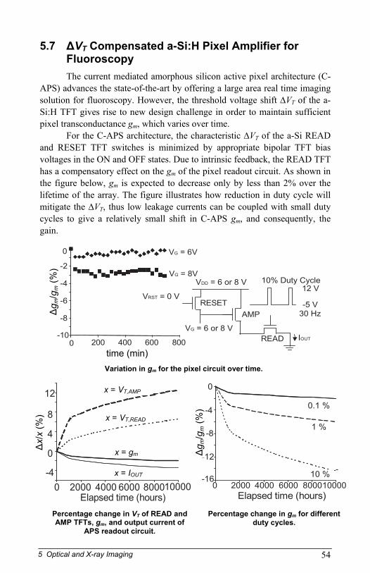
5.7 ΔVT Compensated a-Si:H Pixel Amplifier for Fluoroscopy The current mediated amorphous silicon active pixel architecture (C-
APS) advances the state-of-the-art by offering a large area real time imaging solution for fluoroscopy. However, the threshold voltage shift ∆VT of the a-Si:H TFT gives rise to new design challenge in order to maintain sufficient pixel transconductance gm, which varies over time.
For the C-APS architecture, the characteristic ∆VT of the a-Si READ and RESET TFT switches is minimized by appropriate bipolar TFT bias voltages in the ON and OFF states. Due to intrinsic feedback, the READ TFT has a compensatory effect on the gm of the pixel readout circuit. As shown in the figure below, gm is expected to decrease only by less than 2% over the lifetime of the array. The figure illustrates how reduction in duty cycle will mitigate the ∆VT, thus low leakage currents can be coupled with small duty cycles to give a relatively small shift in C-APS gm, and consequently, the gain.
200-10
-8
-6
-4
-2
0
0 400 600 800t im e (m in )
(Δgm
)/gm(%
)
VG = 6V
VG = 8V
VRST = 0 V
VDD = 6 or 8 V
VG = 6 or 8 V
RESET
READ
AMP
12 V
-5 V30 Hz
10% Duty Cycle
IOUT
Δg m
/gm (%
)
time (min)
Variation in gm for the pixel circuit over time.
-4
0
4
8
12
0 2000 4000 6000 800010000Elapsed time (hours)
VT_AMP
VT_READ
gm
IOUT
% c
hang
e
0x = VT,AMP
-1
-8
-4
% c
hang
e
2
0 2000 4000 6000 800010000
0.1 %
1 %
Δx/
x (%
)
Δg m
/gm (%
)
x =x = VT,READ
x =x = gm
x =x = IOUT 10 %
Elapsed time (hours)
-16
Percentage change in VT of READ and AMP TFTs, gm, and output current of
APS readout circuit.
Percentage change in gm for different duty cycles.
54
5 Optical and X-ray Imaging
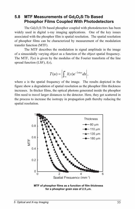
5.8 MTF Measurements of Gd2O2S:Tb Based Phosphor Films Coupled With Photodetectors The Gd2O2S:Tb based phosphor coupled with photodetectors has been
widely used in digital x-ray imaging applications. One of the key issues associated with the phosphor film is spatial resolution. The spatial resolution of phosphor films can be characterized by measurement of the modulation transfer function (MTF).
The MTF describes the modulation in signal amplitude in the image of a sinusoidally varying object as a function of the object spatial frequency. The MTF, T(u) is given by the modulus of the Fourier transform of the line spread function (LSF), l(x),
∫∞
∞−
−= dxexluT iuxπ2)()( ,
where u is the spatial frequency of the image. The results depicted in the figure show a degradation of spatial resolution as the phosphor film thickness increases. In thicker films, the optical photons generated inside the phosphor film need to travel larger distances to the detector. Here, they get scattered in the process to increase the isotropy in propagation path thereby reducing the spatial resolution.
0
0.2
0.4
0.6
0.8
1
0 2 4 6
80 m
110 m
135 m
180 m
Thickness
MT
F
Spatial Frequency (mm )-1
MTF of phosphor films as a function of film thickness for a phosphor grain size of 2.5 μm.
55
5 Optical and X-ray Imaging
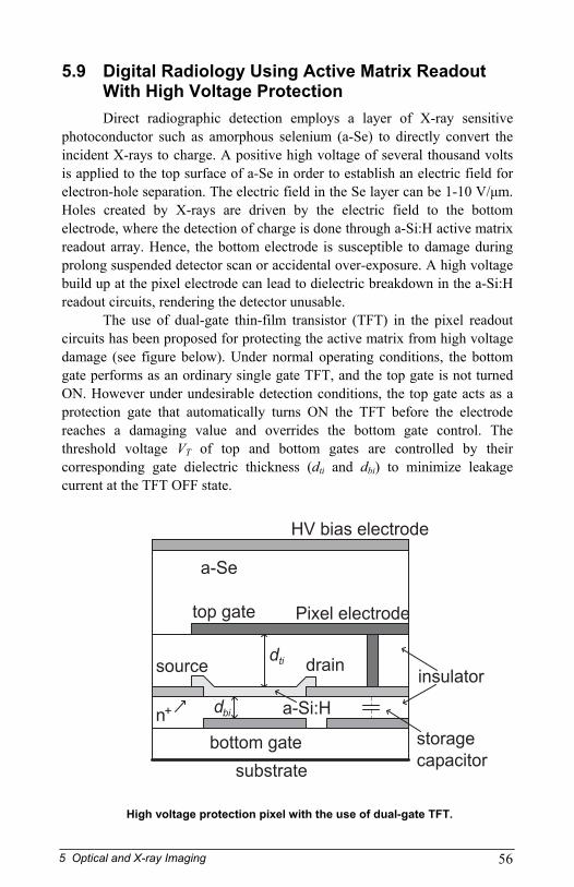
5.9 Digital Radiology Using Active Matrix Readout With High Voltage Protection Direct radiographic detection employs a layer of X-ray sensitive
photoconductor such as amorphous selenium (a-Se) to directly convert the incident X-rays to charge. A positive high voltage of several thousand volts is applied to the top surface of a-Se in order to establish an electric field for electron-hole separation. The electric field in the Se layer can be 1-10 V/μm. Holes created by X-rays are driven by the electric field to the bottom electrode, where the detection of charge is done through a-Si:H active matrix readout array. Hence, the bottom electrode is susceptible to damage during prolong suspended detector scan or accidental over-exposure. A high voltage build up at the pixel electrode can lead to dielectric breakdown in the a-Si:H readout circuits, rendering the detector unusable.
The use of dual-gate thin-film transistor (TFT) in the pixel readout circuits has been proposed for protecting the active matrix from high voltage damage (see figure below). Under normal operating conditions, the bottom gate performs as an ordinary single gate TFT, and the top gate is not turned ON. However under undesirable detection conditions, the top gate acts as a protection gate that automatically turns ON the TFT before the electrode reaches a damaging value and overrides the bottom gate control. The threshold voltage VT of top and bottom gates are controlled by their corresponding gate dielectric thickness (dti and dbi) to minimize leakage current at the TFT OFF state.
substrate
bottom gate
Pixel electrodetop gate
a-Se
storage
capacitor
HV bias electrode
source draindti
n+
insulator
dbi a-Si:H
High voltage protection pixel with the use of dual-gate TFT.
56
5 Optical and X-ray Imaging

6 Photovoltaics
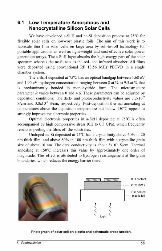
6.1 Low Temperature Amorphous and Nanocrystalline Silicon Solar Cells We have developed a-Si:H and nc-Si deposition process at 75ºC for
flexible solar cells on low-cost plastic foils. The aim of this work is to fabricate thin film solar cells on large area by roll-to-roll technology for portable applications as well as light-weight and cost-effective solar power generation arrays. The a-Si:H layer absorbs the high-energy part of the solar spectrum whereas the nc-Si acts as the red- and infrared absorber. All films were deposited using conventional RF 13.56 MHz PECVD in a single chamber system.
The a-Si:H deposited at 75ºC has an optical bandgap between 1.68 eV and 1.90 eV, hydrogen concentration ranging between 8 at.% to 9.5 at.% that is predominantly bonded in monohydride form. The microstructure parameter R varies between 0 and 4.6. These parameters can be adjusted by deposition conditions. The dark- and photoconductivity values are 3.2x10⁻⁹ S/cm and 3.8x10⁻⁵ S/cm, respectively. Post-deposition thermal annealing at temperatures above the deposition temperature but below 150ºC appear to strongly improve the electronic properties.
Optimal electronic properties in a-Si:H deposited at 75ºC is often accompanied by high compressive stress (0.2 to 0.5 GPa), which frequently results in peeling the films off the substrates.
Undoped nc-Si deposited at 75ºC has a crystallinity above 60% in 20 nm thick film, and above 80% in 100 nm thick film with a crystallite grain size of about 10 nm. The dark conductivity is about 3x10⁻⁷ S/cm. Thermal annealing at 150ºC increases this value by approximately one order of magnitude. This effect is attributed to hydrogen rearrangement at the grain boundaries, which reduces the energy barrier there.
ITO contact
ITO coated plastic foil
p-i-n layers
Light
Photograph of solar cell on plastic and schematic cross section.
58
6 Photovoltaics
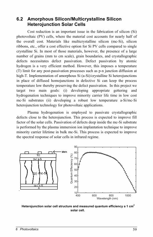
6.2 Amorphous Silicon/Multicrystalline Silicon Heterojunction Solar Cells Cost reduction is an important issue in the fabrication of silicon (Si)
photovoltaic (PV) cells, where the material cost accounts for nearly half of the overall cost. Materials like multicrystalline silicon (mc-Si), silicon ribbons, etc., offer a cost effective option for Si PV cells compared to single crystalline Si. In most of those materials, however, the presence of a large number of grains (mm to cm scale), grain boundaries, and crystallographic defects necessitates defect passivation. Defect passivation by atomic hydrogen is a very efficient method. However, this imposes a temperature (T) limit for any post-passivation processes such as p-n junction diffusion at high-T. Implementation of amorphous Si (a-Si)/crystalline Si heterojunctions in place of diffused homojunctions in defective Si can keep the process temperature low thereby preserving the defect passivation. In this project we target two main goals: (i) developing appropriate gettering and hydrogenation techniques to improve minority carrier life time in low cost mc-Si substrates (ii) developing a robust low temperature a-Si/mc-Si heterojunction technology for photovoltaic applications.
Plasma hydrogenation is employed to passivate crystallographic defects close to the heterojunction. This process is expected to improve fill factor of the solar cells. Passivation of defects deep inside the mc-Si substrate is performed by the plasma immersion ion implantation technique to improve minority carrier lifetime in bulk mc-Si. This process is expected to improve the spectral response of solar cells in infrared regime.
Quantu
mE
ffecie
ncy
(%)
Wavelength (nm)
90
80
70
60
50
40
30
20
10400 600 800 1000
Heterojunction solar cell structure and measured quantum efficiency a 1 cm2 solar cell.
59
6 Photovoltaics
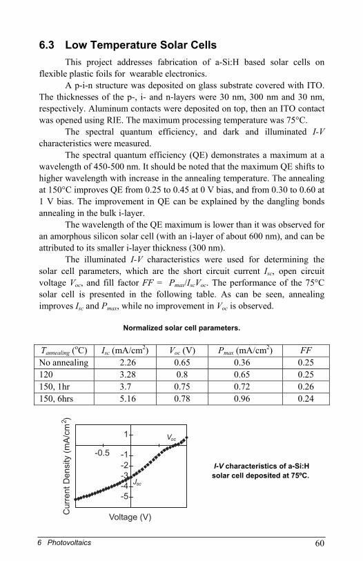
6.3 Low Temperature Solar Cells This project addresses fabrication of a-Si:H based solar cells on
flexible plastic foils for wearable electronics. A p-i-n structure was deposited on glass substrate covered with ITO.
The thicknesses of the p-, i- and n-layers were 30 nm, 300 nm and 30 nm, respectively. Aluminum contacts were deposited on top, then an ITO contact was opened using RIE. The maximum processing temperature was 75°C.
The spectral quantum efficiency, and dark and illuminated I-V characteristics were measured.
The spectral quantum efficiency (QE) demonstrates a maximum at a wavelength of 450-500 nm. It should be noted that the maximum QE shifts to higher wavelength with increase in the annealing temperature. The annealing at 150°C improves QE from 0.25 to 0.45 at 0 V bias, and from 0.30 to 0.60 at 1 V bias. The improvement in QE can be explained by the dangling bonds annealing in the bulk i-layer.
The wavelength of the QE maximum is lower than it was observed for an amorphous silicon solar cell (with an i-layer of about 600 nm), and can be attributed to its smaller i-layer thickness (300 nm).
The illuminated I-V characteristics were used for determining the solar cell parameters, which are the short circuit current Isc, open circuit voltage Voc, and fill factor FF = Pmax/IscVoc. The performance of the 75°C solar cell is presented in the following table. As can be seen, annealing improves Isc and Pmax, while no improvement in Voc is observed.
Normalized solar cell parameters.
Tannealing (oC) Isc (mA/cm2) Voc (V) Pmax (mA/cm2) FF No annealing 2.26 0.65 0.36 0.25 120 3.28 0.8 0.65 0.25 150, 1hr 3.7 0.75 0.72 0.26 150, 6hrs 5.16 0.78 0.96 0.24
-5
-4
-3
-2
-1
1
-0.5
Voltage (V)
Curr
entD
ensity
(mA
/cm
)2
Voc
Jsc
I-V characteristics of a-Si:H solar cell deposited at 75ºC.
60
6 Photovoltaics
Publications Papers to Appear [1] K. Sakariya, C. Ng., P. Servati, A. Nathan, "Accelerated stress testing of a-Si:H
pixel circuits for AMOLED displays," IEEE Trans. on Electron Devices, 2005, to appear.
[2] A. Nathan, G.R. Chaji, S.J. Ashtiani, "Driving schemes for a-Si and LTPS AMOLED displays," (INVITED) IEEE/OSA J. of Display Technology, 2005, to appear.
[3] G.R. Chaji, A. Nathan, "A fast settling current driver based on the CCII for AMOLED displays," IEEE/OSA J. of Display Technology, 2005, to appear.
[4] C.-H. Lee, A. Sazonov, A. Nathan, “High hole and electron mobilities in nanocrystalline silicon thin-film transistors,” J. Non-Crys. Solids, to appear.
[5] N. Safavian, G.R. Chaji, A. Nathan, J. A. Rowlands, “Parameter compensated active pixel sensor array for digital x-ray fluoroscopy in a-Si:H technology,” J. Vac. Sci. Technol. A, to appear.
[6] G. R. Chaji, N. Safavian, A. Nathan, J. A. Rowlands, “Stable a-Si:H circuits based on short-term stress stability of amorphous silicon TFTs,” J. Vac. Sci. Technol. A, to appear.
[7] S. Sambandan, K. Sakariya, A. Kumar, P. Servati, A. Nathan, “Voltage controlled current source for AMOLED displays, IEEE Trans. Electron Devices, 2005, to appear.
[8] A. Kumar, A. Nathan, G. E. Jabbour, "Does TFT mobility impact pixel sizes in AMOLED backplanes?," IEEE Trans. on Electron Devices, vol. 52 (2005) in press.
[9] S.J. Ashtiani, P. Servati, D. Striakhilev, and A. Nathan, “A 3-TFT current-programmed pixel circuit for active-matrix organic light-emitting diode displays,” IEEE Trans. Electron Devices.
[10] S.M. Jahinuzzaman, A. Sultana, K. Sakariya, P. Servati, and A. Nathan, “Stress induced short and long term instability in a-Si:H thin film transistors,” Appl. Phys. Lett.
[11] S. Ali, M. Gharghi, S. Sivoththaman, and K. Zeaiter, “Properties and characterization of low-temperature amorphous PECVD silicon nitride films for solar cell passivation,” J. Mat. Sci.
[12] A. Sazonov, M. Meitine, and D. Striakhilev, “Low temperature materials and thin film transistors for flexible electronics,” IEEE Proc. Flexible Electronics Technology.
[13] G.R. Chaji, D. Striakhilev, and A. Nathan, "A novel a-Si:H AMOLED pixel circuit based on short-term stress stability of a-Si:H TFTs," IEEE Electron Device letts., to be published.
[14] A. Nathan, G.R. Chaji, and S.J. Ashtiani, "Driving schemes for a-Si and LRPS AMOLED displays," IEEE J. of Display Technology, to be published.
[15] G.R. Chaji and Arokia Nathan, "A fast settling current driver based on the CCII for AMOLED displays," IEEE J. of Display Technology, submitted on July 2005.
61
Publications
[16] S. Fathololoumi, I. Chan, M. Moradi, A. Nathan, “A study on nanoscale channel thin film transistor”, Canada Nano Forum 2005.
[17] S. Fathololoumi, I. Chan, M. Moradi, A. Nathan, “A Numerical Study on Scaling of a-Si:H Thin Film Transistors”, J. Vac. Sci. Tech., 2005.
[18] A.Sazonov, M.Meitine, D.Striakhilev, and A.Nathan, “Low Temperature Amorphous and Nanocrystalline Silicon Based TFTs for Flexible Electronics,” submitted to Semiconductors (April 2005), 39 pages (in Russian).
[19] K. Bayat (Student), Y. Vygranenko, A. Sazonov, and M.F. Baroughi, “Design, Fabrication and Characterization of Highly Selective a-Si:H Based UV Detector for Sunburn Applications,” submitted to J.Vac.Sci.Technol.A (July 2005).
[20] G.R. Chaji, D. Striakhilev, A. Nathan, "A novel a-Si:H AMOLED pixel circuit based on short-term stress stability of a-Si:H TFTs," IEEE Electron Device Letters, to appear.
[21] S. Sambandan, L. Zhu, D. Striakhilev, P. Servati, “Markov model for threshold voltage shift in amorphous silicon TFTs for variable gate bias, IEEE Electron Device Letters, 2005, to appear.
[22] C.-H. Lee, A. Sazonov, A. Nathan, “High mobility n-channel and p-channel nanocrystalline silicon thin film transistors,” Technical Digest, IEEE IEDM, Washington, DC, USA, Dec. 5-8, 2005, in press.
[23] D. Striakhilev, A. Nathan, P. Servati, A. Sazonov, “Amorphous silicon integration on plastic for flexible AMOLED displays”, (INVITED) Proc. 207th Meeting of the Electrochemical Society, Quebec City, May 16-19, 2005, to appear.
[24] N. Safavian, J. Lai, J. Rowlands, A. Nathan, “Active pixel sensor array for digital x-ray imaging in a-Si:H technology”, Proc. 207th Meeting of the Electrochemical Society, Quebec City, May 16-19, 2005, to appear.
[25] G.R. Chaji, A. Nathan, "A novel driving scheme for high-resolution large-area a-Si:H AMOLED displays," IEEE Midwest Symposium on Circuits and Systems, Cincinnati, USA, August 7-10, 2005, in press.
[26] G.R. Chaji, N. Safavian, A. Nathan, "Dynamic-effect compensating technique for stable a-Si:H AMOLED displays," IEEE Midwest Symposium on Circuits and Systems, Cincinnati, USA, August 7-10, 2005, in press.
[27] N. Safavian, G.R. Chaji, S. J. Ashtiani, A. Nathan, and J. A. Rowlands, "Self-compensated a-Si:H detector with current-mode readout circuit for digital x-ray fluoroscopy," IEEE Midwest Symposium on Circuits and Systems, Cincinnati, USA, August 7-10, 2005, in press.
Refereed Papers 2005 [28] S. Alexander, P. Servati, G.R. Chaji, S. Ashtiani. R. Hung, D. Striakhilev, K.
Sakariya, A. Kumar, A. Nathan, C. Church, J. Wzorek, P. Aresnault, "Pixel circuits and drive schemes for glass and elastic AMOLED displays," SID J. of Displays, vol. 7 (2005) 587-595.
62
Publications
[29] S.J. Ashtiani, P. Servati, D. Striakhilev, A. Nathan, “A 3-TFT current-programmed pixel circuit for active-matrix organic light-emitting diode displays” IEEE Trans. Electron Devices, vol. 52 (2005) 1514-1518.
[30] J. Lai, A. Nathan, “Reset and partition noise in active pixel image sensors,” IEEE Trans. Electron Devices, vol. 52 (2005) 2329-2332.
[31] A. Sazonov, C-H. Lee, D. Striakhilev, A. Nathan, "Low temperature materials and thin film transistors for flexible electronics," Proc. IEEE, Special Issue on Flexible Electronics Technology, vol. 93 (2005) 1420.
[32] P. Servati, A. Nathan, “Functional pixel circuits for elastic AMOLED displays,” (INVITED) Proc. IEEE, Special Issue on Flexible Electronics Technology, vol. 93 (2005) 1257-1264.
[33] F.M. Li, S. Koul, Y. Vygranenko, P. Servati, A. Nathan, “Dual-Gate SiO2/P3HT/SiNx OTFT,” Mat. Res. Soc. Symp. Proc., vol. 871E (2005) I9.4.1-I9.4.6.
[34] F.M. Li, S. Koul, Y. Vygranenko, A. Sazonov, P. Servati and A. Nathan, “Fabrication of RR-P3HT-based TFTs using low-temperature PECVD silicon nitride,” Mat. Res. Soc. Symp. Proc., vol. 871E (2005) I9.3.1-I9.3.6.
[35] J. Lai, N. Safavian, A. Nathan, J.A. Rowlands, “Active pixel TFT arrays for digital fluoroscopy in a-Si:H technology,” Mat. Res. Soc. Symp. Proc., 2005, to appear.
[36] C.-H. Lee, D.J. Grant, A. Sazonov, A. Nathan, “Post-deposition thermal annealing and material stability of 75C hydrogenated nanocrystalline silicon PECVD films,” J. Appl. Phys., vol. 98 (2005) 034305.
[37] C.-H. Lee, A. Sazonov, A. Nathan, “High electron mobility (~150 cm2/Vs) PECVD nanocrystalline silicon top-gate TFTs at 260C,” Mat. Res. Soc. Symp. Proc., vol. 862 (2005) A17.5.
[38] Yu. Vygranenko, J.H. Chang, A. Nathan, “Two-dimensional a-Si:H/a-SiC:H n-i-p sensor array with ITO/a-SiNx antireflection coating”, Mat. Res. Soc. Symp. Proc., vol. 862 (2005) A9.4.1-A9.4.6.
[39] C.-H. Lee, A. Sazonov, A. Nathan, “Effects of post annealing and material stability of undoped and n+ nc-Si:H film deposited at 75C using 13.56 MHz PECVD,” Mat. Res. Soc. Symp. Proc., vol. 862 (2005), A5.4.
[40] Yu. Vygranenko, J.H. Chang, A. Nathan, "Two-dimensional a-Si:H n-i-p photodiode array low-level light detection," IEEE J. Quantum Electronics, vol. 41 (2005) 697-703.
[41] G.R. Chaji, P. Servati, and A. Nathan, “A new driving scheme for the stable operation of the 2-TFT a-Si AMOLED pixel,” IEE electronic letters, vol. 41, no. 8, pp. 499-500, April 2005.
[42] N. Safavian, J. Lai, J.A. Rowlands, A. Nathan, “Active pixel TFT arrays for digital fluoroscopy in a-Si:H Technology,” IEEE Electronics Letters, vol 41 (2005) 41-42.
[43] G.R. Chaji, P. Servati, A. Nathan, “A new driving scheme for the stable operation of the 2-TFT a-Si AMOLED pixel,” IEE Electronic Letters, vol. 41 (2005) 499-500.
63
Publications
[44] C.-H. Lee, D. Striakhilev, S. Tao, A. Nathan, “Top-gate TFTs using 13.56 MHz PECVD microcrystalline silicon,” IEEE Electron Device Letters, vol. 26 (2005) 637-639.
[45] S.M. Jahinuzzaman, A. Sultana, K. Sakariya, P. Servati, A. Nathan, “Threshold voltage instability of amorphous silicon thin-film transistors under constant current stress,” Appl. Phys. Lett., vol. 87 (2005) 23502 (3 pages).
[46] C.-H. Lee, A. Sazonov, A. Nathan, “High-mobility nanocrystalline silicon thin-film transistors fabricated by plasma-enhanced chemical vapor deposition,” Appl. Phys. Lett., vol. 86 (2005) 222106 (3 pages). (also appeared in Virtual J. Nanoscale Science & Technology vol. 11, Issue 22, 2005).
[47] I. Chan, A. Nathan, “Amorphous silicon thin film transistors with 90 vertical nanoscale channel,” Appl. Phys. Lett., vol. 86 (2005) 253501 (3 pages).
[48] N. Safavian, J. Lai, J. Rowlands, and A. Nathan, “Threshold voltage shift compensated active pixel sensor array for digital x-ray imaging in a-Si technology,” Electronics Letters, vol. 41 (2005) 441-442.
[49] S. Sambandan, A. Kumar, K. Sakariya, A. Nathan, “Analogue building blocks with amorphous silicon thin film transistors,” Electronics Letters, vol. 41 (2005) 314-315.
[50] G.R. Chaji, P. Servati, A. Nathan, “Driving scheme for stable operation of 2-TFT a-Si AMOLED pixel,” Electronics Letters, vol. 41 (2005) 499-500.
[51] P. Servati, A. Nathan, "Orientation-dependent strain-tolerance of amorphous silicon transistors and pixel circuits for elastic active-matrix organic light-emitting diode display," Appl. Phys. Lett., vol. 36 (2005) 33504-1-3.
2004 [52] M.F. Baroughi and S. Sivoththaman, “Effects of grain boundaries in
amorphous/multicrystalline silicon heterojunction photovoltaic cells,” Mat. Res. Soc. Symp. Proc., vol. 836 (2004) in press.
[53] P. Servati, Y. Vygranenko, A. Nathan, S. Morrison, and A. Madan, “Low dark current and blue-enhanced a-Si:H/a-SiC:H heterojunction n-i-δi-p photodiode image sensor,” J. Appl. Phys., vol. 96 (2004) 7575-7582.
[54] A. Sazonov and C. McArthur, “Sub-100ºC a-Si:H TFTs on plastic substrates with silicon nitride gate dielectrics,” J. Vac. Sci. Technol. A, vol. 22 (2004) 2052-2055.
[55] M.F. Baroughi, R. Jeyakumar, Y. Vygranenko, F. Khalvati, and S. Sivoththaman, “Fabrication and characterization of amorphous Si/crystalline Si heterojunction devices for photovoltaic applications,” J. Vac. Sci. Technol. A, vol. 22 (2004) 1015-1019.
[56] I. Chan and A. Madan, “100-nm channel length a-Si:H vertical thin film transistors,” Mat. Res. Soc. Symp. Proc., vol. 808 (2004) A3.4/I2.4.
[57] M. Meitine and A. Sazonov, “Top gate TFT for large area electronics,” Mat. Res. Soc. Symp. Proc., vol. 814 (2004) I6.12.
[58] P. Servati, Y. Vygranenko, A. Nathan, S. Morrison, A. Madan, "Low dark current and blue-enhanced a-Si:H/a-SiC:H heterojunction n-i-di-p photodiode image sensor," J. Appl. Phys., vol. 96 (2004) 7575-7582.
64
Publications
[59] K. Sakariya, P. Servati, A. Nathan, "Stability analysis of current programmed a-Si:H AMOLED pixel circuits," IEEE Trans. Electron Devices, vol. 51 (2004) 2019-2025.
[60] F.M. Li, N. O, A. Nathan, "Degradation behavior and damage mechanisms of CCD image sensor with deep-UV laser radiation," IEEE Trans. Electron Devices, vol. 51 (2004) 2229-2236.
[61] A. Nathan, A. Kumar, K. Sakariya, P. Servati, S. Sambandan, K.S. Karim, D. Striakhilev, "Amorphous silicon thin film transistor circuit integration for organic LED displays on glass and plastic," (INVITED) IEEE J. Solid-State Circuits, vol. 39 (2004) 1477-1486.
[62] K.S. Karim, P. Servati, A. Nathan, "High voltage amorphous silicon TFT for use in large area applications," Microelectron. J., vol. 35 (2004) 311-315.
[63] C.-H. Lee, Y. Vygranenko, A. Nathan, "Process isuues with Mo/a-Si:H Schottky diode and TFT integration for direct X-ray detection," J. Vac. Sci. Technol. A, vol. 22 (2004) 2091-2095.
[64] J.H. Chang, Y. Vygranenko, A. Nathan, "Two-dimensional a-Si:H based n-i-p sensor array," J. Vac. Sci. Technol. A, vol. 22 (2004) 971-974.
[65] A. Kumar, S. Sambandan, K. Sakariya, P. Servati, A. Nathan, "Amorphous silicon shift registers for display drivers," J. Vac. Sci. Technol. A, vol. 22 (2004) 981-986.
[66] J. Lai, A. Nathan, "Reset noise in active pixel image sensors," J. Vac. Sci. Technol. A, vol. 22 (2004) 987-990.
[67] C.-H. Lee, D. Striakhilev, A. Nathan, "Highly conductive n+ hydrogenated microcrystalline silicon and its application in thin film transistors," J. Vac. Sci. Technol. A, vol. 22 (2004) 991-995.
[68] F. Li, A. Nathan, N. O, "Deep-ultraviolet-induced damage of charge coupled device sensors," J. Vac. Sci. Technol. A, vol. 22 (2004) 996-1000.
[69] K. Sakariya, S. Sambandan, P. Servati, A. Nathan, "Analysis and characterization of self-compensating current programmed a-Si:H active matrix organic light-emitting diode pixel circuits," J. Vac. Sci. Technol. A, vol. 22 (2004) 1001-1004.
[70] K.S. Karim, A. Nathan, "Noise performance of a current-mediated amplified pixel for large-area medical imaging," J. Vac. Sci. Technol. A, vol. 22 (2004) 1010-1014.
[71] I. Chan, A. Nathan, "Thick film resist lithography for a-Si:H devices with high topography and long dry etch processes," J. Vac. Sci. Technol. A, vol. 22 (2004) 1048-1053.
[72] I. Chan, A. Nathan, "100-nm channel length a-Si:H vertical thin film transistors," Mat. Res. Soc. Symp. Proc., vol. 814, 2004, pp. 35-40.
[73] D.J. Grant, C.-H. Lee, A. Nathan, U.K. Das, A. Madan, "Bottom-gate TFTs with channel layer grown by pulsed PECVD technique," Mat. Res. Soc. Symp. Proc., vol. 808 (2004) A4.8.
[74] K. Sakariya, C. Ng, I. Huang, A. Sultana, S. Tao, A. Nathan, "Accelerated stress testing of a-Si:H TFT pixel circuits for AMOLED displays," Mat. Res. Soc. Symp. Proc., vol. 808 (2004) A4.11.1-A4.11.6.
65
Publications
[75] C.-H. Lee, D. Striakhilev, A. Nathan, "Intrinsic and doped µc-Si:H layers using 13.56 MHz PECVD at 250ºC," Mat. Res. Soc. Symp. Proc., vol. 808 (2004) A4.14.
[76] C.-H. Lee, A. Sazonov, A. Nathan, "Low temperature (75ºC) hydrogenated nanocrystalline silicon films grown by conventional plasma enhanced chemical vapor deposition for thin film transistors," Mat. Res. Soc. Symp. Proc., vol. 808 (2004) A4.17.
[77] A. Nathan, D. Striakhilev, P. Servati, K. Sakariya, A. Sazonov, S. Alexander, S. Tao, C.-H. Lee, A. Kumar, S. Sambandan, S. Jafarabadiashtiani, Y. Vygranenko, I.W. Chan, "A-Si AMOLED display backplanes on flexible substrates," (INVITED) Mat. Res. Soc. Symp. Proc., vol. 814 (2004) 61-72.
[78] P. Servati, S. Tao, E. Horne, D. Striakhilev, A. Nathan, "Mechanically strained a-Si:H AMOLED driver circuits," Mat. Res. Soc. Symp. Proc., vol. 814 (2004) I6.13.1-I6.13.6.
[79] S. Koul, A. Nathan, "An optimized synthetic route for the preparation of water-soluble nanomagnetic conducting polyaniline with high processability," Mat. Res. Soc. Symp. Proc., vol. 818 (2004) M11.24.
[80] A. Nathan, A. Kumar, K. Sakariya, P. Servati, K.S. Karim, D. Striakhilev, A. Sazonov, "Amorphous silicon back-plane electronics for OLED displays," (INVITED) IEEE J. Selected Topics in Quantum Electron., vol. 10 (2004) 58-69.
[81] S.J. Ashtiani, P. Servati, A. Nathan, "An active-matrix organic light-emitting diode display driver based on second-generation current conveyor," Electronics Letters, vol. 40 (2004) 1178-1179.
[82] K.S. Karim, A. Nathan, M. Hack, W.I. Milne, “Drain-bias dependence of threshold voltage stability of amorphous silicon TFTs,” IEEE Electron Device Letters, vol. 25 (2004) 188-190.
2003 [83] M.F. Baroughi and S. Sivoththaman, “Role of interface quality and film doping
density in amorphous Si/crystalline Si heterojunctions for photovoltaic applications,” Mat. Res. Soc. Symp. Proc., vol. 796 (2003) V2.11.
[84] M. Meitine and A. Sazonov, “Low temperature PECVD silicon oxide for devices and circuits on flexible substrates,” Mat. Res. Soc. Symp. Proc., vol. 769 (2003) 165-170.
[85] C. McArthur, M. Meitine, and A. Sazonov, “Optimization of 75°C amorphous silicon nitride for TFTs on plastics,” Mat. Res. Soc. Symp. Proc., vol. 769 (2003) 303-308.
[86] A. Nathan, P. Servati, K.S. Karim, D. Striakhilev, A. Sazonov, “Thin film transistor integration on glass and plastic substrates in amorphous silicon technology,” (INVITED) IEE Proc.-Circuits Devices Syst., vol. 150 (2003) 329-338. (won the IEE Institution Premium for the Best Paper in 2002/2003 Circuits, Devices, and Systems.)
66
Publications
[87] K.S. Karim, A. Nathan, J.A. Rowlands, S.O. Kasap, "X-ray detector with on-pixel amplification for large area diagnostic medical imaging," IEE Proc.-Circuits Devices Syst., vol. 150 (2003) 267-273.
[88] A. Kumar, K. Sakariya, P. Servati, S. Alexander, D. Striakhilev, K. S. Karim, A. Nathan, M. Hack, E. Williams, G.E. Jabbour, "Design considerations for active matrix organic light emitting diode arrays," IEE Proc.-Circuits Devices Syst., vol. 150 (2003) 322-328.
[89] A. Nathan, D. Striakhilev, P. Servati, K. Sakariya, A. Kumar, K.S. Karim, A. Sazonov, “Low temperature a-Si:H pixel circuits for mechanically flexible AMOLED displays,” Mat. Res. Soc. Symp. Proc., vol. 769 (2003) 29-34.
[90] P. Servati, S. Striakhilev, A. Nathan, “Above-threshold parameter extraction including contact resistance effects for a-Si:H TFTs on glass and plastic,” Mat. Res. Soc. Proc. vol. 762 (2003) 187-192.
[91] C.-H. Lee, I. Chan, A. Nathan, “Mechanical stress and process integration for direct X-ray detector and TFT in a-Si:H technology,” Mat. Res. Soc. Proc. vol. 762 (2003) 193-198.
[92] K.S. Karim, K. Sakariya, A. Nathan, “Threshold voltage performance of a-Si:H TFTs for analog applications,” Mat. Res. Soc. Proc. vol. 762 (2003) 247-252.
[93] S. Tao, Y. Vygranenko, A. Nathan, “ Enhanced blue sensitivity in ITO/a-SiNx:H/a-Si:H MIS photodetectors,” Mat. Res. Soc. Proc. vol. 762 (2003) 277-282.
[94] P. Servati, S. Striakhilev, A. Nathan, “Above-threshold parameter extraction and modeling for amorphous silicon thin film transistors,” IEEE Trans. Electron Devices, vol. 50 (2003) 2227-2235.
[95] Wendy A. R. Franks, Martin J. Kiik, “UV-Responsive CCD image sensors with enhanced inorganic phosphor coatings,” IEEE Trans. Electron Devices, vol 50 (2003) 352–358.
[96] P. Servati, K.S. Karim, A. Nathan, “Static characteristics of a-Si:H dual gate TFTs,” IEEE Trans. Electron Devices, vol. 50 (2003) 926–932.
[97] K.S. Karim, A. Nathan, J.A. Rowlands, “Amorphous silicon active pixel sensor readout circuit for digital imaging”, IEEE Trans. Electron Devices, vol. 50 (2003) 200-208.
2002 [98] J. Horzel, C. Allebe, J. Szlufcik, S. Sivoththaman, "Develpment of RTP
for industrial solar cell processing", Solar Energy Materials & Solar Cells", vol.72, pp.263-269, 2002.
[99] I. Chan, A. Nathan, "Amorphous silicon vertical thin film transistor for high density integration," Mat. Res. Soc. Symp. Proc, vol. 715 (2002) A12.6.1.-A12.6.6.
[100] K.S. Karim, A. Nathan, J.A. Rowlands, "Amorphous silicon active pixel sensor readout circuit architectures for medical imaging," Mat. Res. Soc. Symp. Proc, vol. 715 (2002) A4.2.1 - A4.2.6.
67
Publications
[101] S. Morrison, P. Servati, Y. Vygranenko, A. Nathan, A. Madan, “Reduction of dark current under reverse bias in a-Si:H p-i-n photodetectors,” Mat. Res. Soc. Symp. Proc, vol. 715 (2002) A7.4.1-A7.4.6.
[102] S. Tao, Z.H. Gu, A. Nathan, “Fabrication of Gd2O2S:Tb based phosphor films coupled with photodetectors for X-ray imaging applications, Journal of Vacuum Science & Technology A, vol. 20(3) (2002) 1091-1094.
[103] S. Sivoththaman, R. Jeyakumar, L. Ren, A. Nathan, "Characterization of low permittivity (low-k) dielectric films for low temperature device integration", Journal of Vacuum Science and Technology, vol. 20(3) (2002) 1149-1153.
[104] I. Chan, A. Nathan, "Dry etch process optimization for small-area a-Si:H vertical thin film transistors,” Journal of Vacuum Science and Technology A, vol. 20 (2002) 962-965.
[105] P. Servati, S. Prakash, A. Nathan, Ch. Py, “Amorphous silicon driver circuits for organic light-emitting diode displays,” Journal of Vacuum Science and Technology A, vol. 20(4) (2002) 1374-1378.
[106] P. Servati, A. Nathan, “Modeling of the static and dynamic behavior of a-Si:H TFTs,” Journal of Vacuum Science and Technology A, vol. 20(3) (2002) 1038-1042.
[107] K. S. Karim, A. Nathan, J.A. Rowlands, “Active pixel sensor architectures in a-Si:H for medical imaging,” Journal of Vacuum Science and Technology, vol. 20(3) (2002) 1095-1099.
[108] N. Mohan, K.S. Karim, A. Nathan, “Design of multiplexer in amorphous silicon technology,” Journal of Vacuum Science and Technology A, vol. 20(3) (2002) 1043-1047.
[109] P. Servati, A. Nathan, “Modelling of the reverse characteristics of a-Si:H TFTs,” IEEE Trans. on Electron Devices, vol. 49(5) (2002) 812-819.
[110] A. Nathan, B. Park, Q. Ma, A. Sazonov, J.A. Rowlands, “Amorphous silicon technology for large area digital x-ray and optical imaging,” (INVITED) Microelectronics Reliability, 40th Anniversary Special Issue, vol. 42 (2002) 735-746.
[111] D. Stryahilev, A. Sazonov, A. Nathan, “Amorphous silicon nitride deposited at 120°C for OLED-TFT arrays on plastic substrates,” Journal of Vacuum Science and Technology A, vol. 20 (2002) 1087-1090.
[112] A. Sazonov, D. Stryahilev, A. Nathan, L.D. Bogomolova, “Dielectric performance of low-temperature silicon nitride films in a-Si:H TFTs,” J.Non-Cryst. Solids, vol. 299-302 (2002) 1360-1364.
[113] K.S. Karim, A. Nathan, J.A. Rowlands, “Active pixel sensor architectures for large area medical imaging,” J. Non-Cryst. Solids, vol. 299-302, Part 2 (2002) 1250-1255.
[114] L.D. Bogomolova, V.A. Jachkin, S.A. Prushinsky, D. Stryahilev, A. Sazonov, A. Nathan, “EPR spectra of amorphous silicon nitride films grown by low temperature PECVD,” J. Non-Cryst. Solids, vol. 297 (2002) 247-253.
68
Publications
Conference Papers 2005 [115] S. J. Ashtiani, A. Nathan, “A fast driving scheme for a-Si:H AMOLED displays
based on voltage feedback,” IEEE LEOS 2005 Annual Meeting, Sydney, Australia, Oct. 23 – 27, 2005.
[116] M. Gharghi, H. Bai, G. Stevens, S. Sivoththaman, “Modeling and Simulation of Spherical Solar Cells”, Proceedings of the 31st IEEE Photovoltaic Specialists’ Conference (Florida, 2005) p.1177-1180.
[117] S. Chang and S. Sivoththaman, “Low-loss Inductors built on PECVD Amorphous Silicon for RF Integrated Circuits”, Proceedings of the IEEE Canadian Conference on Electrical and Computer Engineering (2005) p.329 – 333. (Best Paper Award)
[118] S. Sivoththaman and M.F. Baroughi, “Cost-effective Silicon-based Solar Cells, Material and Technology Issues”, Proceedings of the International Green Energy Conference (Waterloo, June 2005).
[119] S. Jafarabadiashtiani, G. R. Chaji, S. Sambandan, D. Striakhilev, P. Servati, and A. Nathan, “A new driving method for a-Si AMOLED displays based on voltage feedback,” Technical Digest, Society for Information Display (SID) Symposium, Boston, May 22-27, 2005, vol. 36, pp. 316-319.
[120] N. Safavian, G.R. Chaji, A. Nathan, and J. A. Rowlands, "TFT active image sensor with current-mode readout circuit for digital x-ray fluoroscopy," SPIE Photonics North, Toronto, Canada, September 12-14, 2005, Vol. 5969, 596929-1.
[121] G.R. Chaji, N. Safavian, A. Nathan, “A low-power driving scheme for a-Si:H active-matrix organic light-emitting displays,” Proc., Third International IEEE Northeast Workshop on Circuits and Systems – NEWCAS, June 19-22, 2005, pp. 5-8.
[122] S. Jafarabadiashtiani, P. Servati, and A. Nathan, “A high-speed driver for current-programmed active-matrix OLED displays,” Proc., Third International IEEE Northeast Workshop on Circuits and Systems – NEWCAS, 2005, June 19-22, 2005, pp. 400-403.
[123] A. Sultana, A. Nathan, J.A. Rowlands, “Amorphous silicon based direct x-ray conversion detector for protein structure analysis,” Proc. SPIE, vol. 5969, pp. 524-536, 2005.
[124] G.R. Chaji, S. Ashtiani, S. Alexander, R. Huang, D. Striakhilev, P. Servati, K. Sakariya, A. Kumar, A. Nathan, “Pixel circuits and drive schemes for large-area a-Si AMOLED displays,” Proc. International Display Manufacturing Conference, Taipei, Taiwan, 2005.
2004 [125] M. Gharghi, H. Bai, S. Sivoththaman, and G. Stevens, “Modeling and
simulation of spherical solar cells,” Proc. 31st IEEE Photovoltaic Specialists Conference (PVSC), Florida, USA, 2005, accepted for publication.
69
Publications
[126] H. Bai, M. Gharghi, S. Sivoththaman, G. Stevens, and M. Hammerbacher, “A three-dimensional numerical model for spherical photovoltaic devices,” Tech. Dig. 14th Int. Photovoltaic Science and Engineering Conf. (PVSEC14), Bangkok, Thailand, Jan. 27-Feb. 1, 2004, pp. 769-770.
[127] A. Sazonov and M. Meitine, “Sub-100ºC amorphous and microcrystalline silicon based TFTs for flexible electronics,” Proc. 4th Int. Conf. on Amorphous and Microcrystalline Semiconductors, Saint Petersburg, Russia, July 5-8, 2004, p. 296.
[128] M.F. Baroughi and S. Sivoththaman, “Amorphous Si/multicrystalline Si heterojunctons for photovoltaic device applications,” Proc. 27th International Conference on the Physics of Semiconductors, Flagstaff, Arizona, USA, July 26-30, 2004, pp.
[129] A. Nathan, S. Alexander, K. Sakariya, P. Servati, D. Striakhilev, S. Tao, A. Kumar, S. Sambandan, S. Jafarabadiashtiani, and Y. Vygranenko, “Stable AMOLED displays using a-Si backplanes,” (INVITED) Proc. Asia Display 2004: 24th Int. Display Research Conf., Daegu, Korea, Aug. 23-27, 2004, pp. 343-347.
[130] D. Striakhilev, P. Servati, K. Sakariya, S. Tao, S. Alexander, A. Kumar, Y. Vygranenko, and A. Nathan, “a-Si pixel circuits on plastic substrates for flexible AMOLED displays,” Proc. Asia Display 2004: 24th Int. Display Research Conf., Daegu, Korea, Aug. 23-27, 2004, pp. 746-748.
[131] K. Sakariya, A. Sultana, C. Ng, and A. Nathan, “Accelerated stress testing of a-Si:H TFT pixel circuits for AMOLED displays,” Proc. Asia Display 2004: 24th Int. Display Research Conf., Daegu, Korea, Aug. 23-27, 2004, pp. 749-752.
[132] S. Koul and A. Nathan, “Synthesis of highly processable nanomagnetic conducting polyaniline in presence of dual oxidant-dopant system,” Proc. 11th Int. Conf. Nano Engineering, South Carolina, USA, Aug. 8-14, 2004.
[133] S.M. Jahinuzzaman, P. Servati, and A. Nathan, “Bias induced long term transient in a-Si:H thin film transistors,” Proc. SPIE Photonics North, vol. 5578, Ottawa, Canada, Sept. 26-29, 2004, pp. 315-322.
[134] A. Sultana, K. Sakariya, and A. Nathan, “Current stress metastability in a-Si:H thin film transistors,” Proc. SPIE Photonics North, vol. 5578, Ottawa, Canada, Sept. 26-29, 2004, pp. 343-352.
[135] J. H. Chang, Y. Vygranenko, and A. Nathan, “Two-dimensional sensor array for low-level light detection,” Proc. SPIE Photonics North, vol. 5578, Ottawa, Canada, Sept. 26-29, 2004, pp. 420-427.
[136] A. Nathan, S. Alexander, K. Sakariya, P. Servati, S. Tao, D. Striakhilev, A. Kumar, S. Sambandan, S. Jafarabadiashtiani, Y. Vigranenko, C. Church, J. Wzorek, and P. Arsenault, “Extreme AMOLED backplanes in a-Si with proven stability,” Digest of Society for Information Display (SID), vol. 35, Seattle, USA, May 23-28, 2004, pp. 1508-1511.
[137] K.S. Karim, S. Yin, A. Nathan, J.A. Rowlands, “High dynamic range pixel architectures for diagnostic medical imaging,” in Medical Imaging 2004: Physics of Medical Imaging, M. Yaffe, M. J. Flynn, Editors, SPIE, vol. 5368, pp. 657-667. (Received Best Poster Award).
70
Publications
[138] S. Sambandan, K. Sakariya, P. Servati, A. Kumar, A. Nathan, “Voltage programmed pixel driver for AMOLED displays with a-Si:H TFT backplane,” Proc. SPIE Photonics West Conf., vol. 5363, San Jose, USA, Jan. 24-29, 2004, pp. 16-26.
2003 [139] A. Sazonov, “Materials challenges for TFT on plastic substrates,” Proc. 16th
Annual IEEE Lasers and Electro Optics Society (LEOS) Meeting, vol. 2, Tucson, USA, Oct. 26-30, 2003, pp. 533-534.
[140] K. Sakariya, A. Kumar, P. Servati, D. Striakhilev, A. Sultana, A. Nathan, “Current stress induced metastability in a-Si:H AMOLED pixel circuits,” Proc., 12th International Workshop on the Physics of Semiconductor Devices (IWPSD), Chennai, India, December 16-20, 2003, pp. 1171-1173.
[141] A. Nathan, K. Sakariya, A. Kumar, P. Servati, K.S. Karim, D. Striakhilev, A. Sazonov, “Amorphous silicon TFT circuit integration for OLED displays on glass and plastic,” (INVITED) Proc. IEEE Custom Integrated Circuits Conference, San Jose, CA, Sept. 21-24, 2003, pp. 215-222.
[142] S. Koul, E. Williams, A. Nathan, G.E. Jabbour, "Synthesis of anthracene based copolymers for photonic applications," The 39th IUPAC Congress and the 86th Conference of the Canadian Society for Chemistry, August 10-15, 2003, Ottawa, Canada, Abstract MS.5.004.
[143] F. Li, Nixon O, A. Nathan “CCD Detection of 157 nm photons,” Proc. IEEE Workshop on Charge-Coupled Devices and Advanced Image Sensors, May 15-17, Elmau, Germany, 2003, 6 pages.
2002 [144] A. Nathan, K. Sakariya, K.S. Karim, A. Kumar, P. Servati, A. Kumar, D.
Striakhilev, “a-Si:H back-plane electronics for medical imaging and OLED displays,” (INVITED) Proc. 2002 IEEE Int, Conf. on Semiconductor Electronics, Penang, Malaysia, Dec. 19-21, 2002, pp. 15-21.
[145] A. Nathan, K. Sakariya, A. Kumar, P. Servati, D. Striakhilev, “Thin film driver circuits for OLED displays,” (INVITED), Abstract Book, PHOTONICS 2002, Sixth International Conference on Optoelectronics, Fiber Optics and Photonics, Mumbai, India, Dec. 16-18, 2002, p. 326.
[146] A. Nathan, K. Sakariya, A. Kumar, P. Servati, D. Striakhilev, “Amorphous silicon backplane electronics for OLED displays,” (INVITED) Proc. 2002 IEEE/LEOS Annual Meeting, Glasgow, Scotland, Nov. 10-14, 2002, pp. 303-304.
[147] A. Nathan, P. Servati, and K. S. Karim, “Amorphous silicon TFT circuit integration,” The 2nd Int. Conf. on Semiconductor Technology (ISTC 2002), Tokyo, Sept. 11-14, 2002, Proc. vol. 2002-17, The Electrochemical Society Inc., pp. 18-35.
[148] A. Nathan, P. Servati, K.S. Karim, D. Striakhilev, A. Sazonov, “a-Si:H TFT circuit integration on glass and plastic substrates,” (INVITED) Thin Film
71
Publications
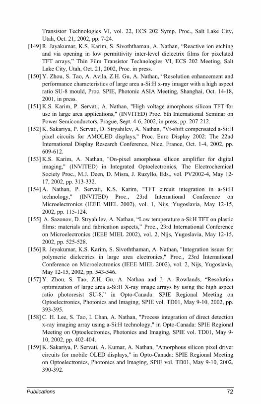
Transistor Technologies VI, vol. 22, ECS 202 Symp. Proc., Salt Lake City, Utah, Oct. 21, 2002, pp. 7-24.
[149] R. Jayakumar, K.S. Karim, S. Sivoththaman, A. Nathan, “Reactive ion etching and via opening in low permittivity inter-level dielectrix films for pixelated TFT arrays,” Thin Film Transistor Technologies VI, ECS 202 Meeting, Salt Lake City, Utah, Oct. 21, 2002, Proc. in press.
[150] Y. Zhou, S. Tao, A. Avila, Z.H. Gu, A. Nathan, “Resolution enhancement and performance characteristics of large area a-Si:H x-ray imager with a high aspect ratio SU-8 mould, Proc. SPIE, Photonic ASIA Meeting, Shanghai, Oct. 14-18, 2001, in press.
[151] K.S. Karim, P. Servati, A. Nathan, "High voltage amorphous silicon TFT for use in large area applications," (INVITED) Proc. 6th International Seminar on Power Semiconductors, Prague, Sept. 4-6, 2002, in press, pp. 207-212.
[152] K. Sakariya, P. Servati, D. Stryahilev, A. Nathan, "Vt-shift compensated a-Si:H pixel circuits for AMOLED displays," Proc. Euro Display 2002: The 22nd International Display Research Conference, Nice, France, Oct. 1-4, 2002, pp. 609-612.
[153] K.S. Karim, A. Nathan, "On-pixel amorphous silicon amplifier for digital imaging," (INVITED) in Integrated Optoelectronics, The Electrochemical Society Proc., M.J. Deen, D. Misra, J. Ruzyllo, Eds., vol. PV2002-4, May 12-17, 2002, pp. 313-332.
[154] A. Nathan, P. Servati, K.S. Karim, "TFT circuit integration in a-Si:H technology," (INVITED) Proc., 23rd International Conference on Microelectronics (IEEE MIEL 2002), vol. 1, Nijs, Yugoslavia, May 12-15, 2002, pp. 115-124.
[155] A. Sazonov, D. Stryahilev, A. Nathan, “Low temperature a-Si:H TFT on plastic films: materials and fabrication aspects,” Proc., 23rd International Conference on Microelectronics (IEEE MIEL 2002), vol. 2, Nijs, Yugoslavia, May 12-15, 2002, pp. 525-528.
[156] R. Jeyakumar, K.S. Karim, S. Sivoththaman, A. Nathan, "Integration issues for polymeric dielectrics in large area electronics," Proc., 23rd International Conference on Microelectronics (IEEE MIEL 2002), vol. 2, Nijs, Yugoslavia, May 12-15, 2002, pp. 543-546.
[157] Y. Zhou, S. Tao, Z.H. Gu, A. Nathan and J. A. Rowlands, “Resolution optimization of large area a-Si:H X-ray image arrays by using the high aspect ratio photoresist SU-8,” in Opto-Canada: SPIE Regional Meeting on Optoelectronics, Photonics and Imaging, SPIE vol. TD01, May 9-10, 2002, pp. 393-395.
[158] C. H. Lee, S. Tao, I. Chan, A. Nathan, "Process integration of direct detection x-ray imaging array using a-Si:H technology," in Opto-Canada: SPIE Regional Meeting on Optoelectronics, Photonics and Imaging, SPIE vol. TD01, May 9-10, 2002, pp. 402-404.
[159] K. Sakariya, P. Servati, A. Kumar, A. Nathan, "Amorphous silicon pixel driver circuits for mobile OLED displays," in Opto-Canada: SPIE Regional Meeting on Optoelectronics, Photonics and Imaging, SPIE vol. TD01, May 9-10, 2002, 390-392.
72
Publications
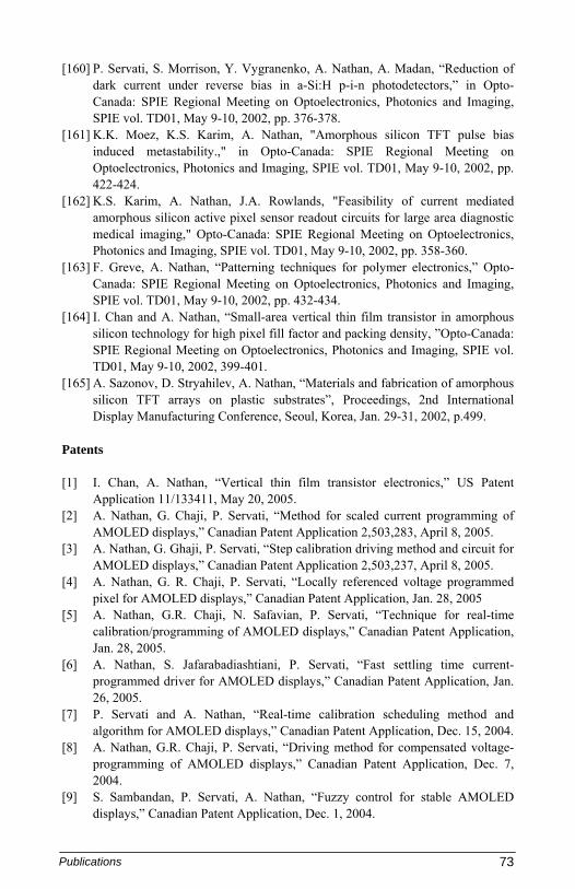
[160] P. Servati, S. Morrison, Y. Vygranenko, A. Nathan, A. Madan, “Reduction of dark current under reverse bias in a-Si:H p-i-n photodetectors,” in Opto-Canada: SPIE Regional Meeting on Optoelectronics, Photonics and Imaging, SPIE vol. TD01, May 9-10, 2002, pp. 376-378.
[161] K.K. Moez, K.S. Karim, A. Nathan, "Amorphous silicon TFT pulse bias induced metastability.," in Opto-Canada: SPIE Regional Meeting on Optoelectronics, Photonics and Imaging, SPIE vol. TD01, May 9-10, 2002, pp. 422-424.
[162] K.S. Karim, A. Nathan, J.A. Rowlands, "Feasibility of current mediated amorphous silicon active pixel sensor readout circuits for large area diagnostic medical imaging," Opto-Canada: SPIE Regional Meeting on Optoelectronics, Photonics and Imaging, SPIE vol. TD01, May 9-10, 2002, pp. 358-360.
[163] F. Greve, A. Nathan, “Patterning techniques for polymer electronics,” Opto-Canada: SPIE Regional Meeting on Optoelectronics, Photonics and Imaging, SPIE vol. TD01, May 9-10, 2002, pp. 432-434.
[164] I. Chan and A. Nathan, “Small-area vertical thin film transistor in amorphous silicon technology for high pixel fill factor and packing density, ”Opto-Canada: SPIE Regional Meeting on Optoelectronics, Photonics and Imaging, SPIE vol. TD01, May 9-10, 2002, 399-401.
[165] A. Sazonov, D. Stryahilev, A. Nathan, “Materials and fabrication of amorphous silicon TFT arrays on plastic substrates”, Proceedings, 2nd International Display Manufacturing Conference, Seoul, Korea, Jan. 29-31, 2002, p.499.
Patents [1] I. Chan, A. Nathan, “Vertical thin film transistor electronics,” US Patent
Application 11/133411, May 20, 2005. [2] A. Nathan, G. Chaji, P. Servati, “Method for scaled current programming of
AMOLED displays,” Canadian Patent Application 2,503,283, April 8, 2005. [3] A. Nathan, G. Ghaji, P. Servati, “Step calibration driving method and circuit for
AMOLED displays,” Canadian Patent Application 2,503,237, April 8, 2005. [4] A. Nathan, G. R. Chaji, P. Servati, “Locally referenced voltage programmed
pixel for AMOLED displays,” Canadian Patent Application, Jan. 28, 2005 [5] A. Nathan, G.R. Chaji, N. Safavian, P. Servati, “Technique for real-time
calibration/programming of AMOLED displays,” Canadian Patent Application, Jan. 28, 2005.
[6] A. Nathan, S. Jafarabadiashtiani, P. Servati, “Fast settling time current-programmed driver for AMOLED displays,” Canadian Patent Application, Jan. 26, 2005.
[7] P. Servati and A. Nathan, “Real-time calibration scheduling method and algorithm for AMOLED displays,” Canadian Patent Application, Dec. 15, 2004.
[8] A. Nathan, G.R. Chaji, P. Servati, “Driving method for compensated voltage-programming of AMOLED displays,” Canadian Patent Application, Dec. 7, 2004.
[9] S. Sambandan, P. Servati, A. Nathan, “Fuzzy control for stable AMOLED displays,” Canadian Patent Application, Dec. 1, 2004.
73
Publications
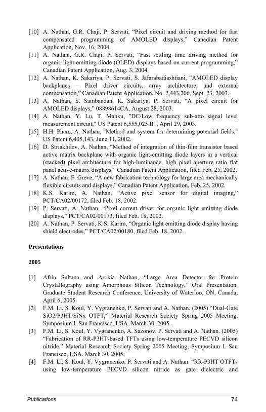
[10] A. Nathan, G.R. Chaji, P. Servati, “Pixel circuit and driving method for fast compensated programming of AMOLED displays,” Canadian Patent Application, Nov. 16, 2004.
[11] A. Nathan, G.R. Chaji, P. Servati, “Fast settling time driving method for organic light-emitting diode (OLED) displays based on current programming,” Canadian Patent Application, Aug. 3, 2004.
[12] A. Nathan, K. Sakariya, P. Servati, S. Jafarabadiashtiani, “AMOLED display backplanes – Pixel driver circuits, array architecture, and external compensation,” Canadian Patent Application, No. 2,443,206, Sept. 23, 2003.
[13] A. Nathan, S. Sambandan, K. Sakariya, P. Servati, “A pixel circuit for AMOLED displays,” 08898614CA, August 28, 2003.
[14] A. Nathan, Y. Lu, T. Manku, "DC/Low frequency sub-atto signal level measurement circuit," US Patent 6,555,025 B1, April 29, 2003.
[15] H.H. Pham, A. Nathan, "Method and system for determining potential fields," US Patent 6,405,143, June 11, 2002.
[16] D. Striakhilev, A. Nathan, “Method of integration of thin-film transistor based active matrix backplane with organic light-emitting diode layers in a vertical (stacked) pixel architecture for high-luminance, high pixel aperture ratio flat panel active-matrix displays,” Canadian Patent Application, filed Feb. 25, 2002.
[17] A. Nathan, F. Greve, “A new fabrication technology for large area mechanically flexible circuits and displays,” Canadian Patent Application, Feb. 25, 2002.
[18] K.S. Karim, A. Nathan, “Active pixel sensor for digital imaging,” PCT/CA02/00172, filed Feb. 18, 2002.
[19] P. Servati, A. Nathan, “Pixel current driver for organic light emitting diode displays,” PCT/CA02/00173, filed Feb. 18, 2002.
[20] A. Nathan, P. Servati, K.S. Karim, “Organic light emitting diode display having shield electrodes,” PCT/CA02/00180, filed Feb. 18, 2002.
Presentations 2005 [1] Afrin Sultana and Arokia Nathan, “Large Area Detector for Protein
Crystallography using Amorphous Silicon Technology,” Oral Presentation, Graduate Student Research Conference, University of Waterloo, ON, Canada, April 6, 2005.
[2] F.M. Li, S. Koul, Y. Vygranenko, P. Servati and A. Nathan. (2005) “Dual-Gate SiO2/P3HT/SiNx OTFT,” Material Research Society Spring 2005 Meeting, Symposium I. San Francisco, USA. March 30, 2005.
[3] F.M. Li, S. Koul, Y. Vygranenko, A. Sazonov, P. Servati and A. Nathan. (2005) “Fabrication of RR-P3HT-based TFTs using low-temperature PECVD silicon nitride,” Material Research Society Spring 2005 Meeting, Symposium I. San Francisco, USA. March 30, 2005.
[4] F.M. Li, S. Koul, Y. Vygranenko, P. Servati and A. Nathan. “RR-P3HT OTFTs using low-temperature PECVD silicon nitride as gate dielectric and
74
Publications
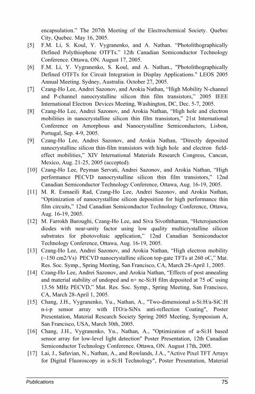
encapsulation.” The 207th Meeting of the Electrochemical Society. Quebec City, Quebec. May 16, 2005.
[5] F.M. Li, S. Koul, Y. Vygranenko, and A. Nathan. “Photolithographically Defined Polythiophene OTFTs.” 12th Canadian Semiconductor Technology Conference. Ottawa, ON. August 17, 2005.
[6] F.M. Li, Y. Vygranenko, S. Koul, and A. Nathan., "Photolithographically Defined OTFTs for Circuit Integration in Display Applications." LEOS 2005 Annual Meeting. Sydney, Australia. October 27, 2005.
[7] Czang-Ho Lee, Andrei Sazonov, and Arokia Nathan, “High Mobility N-channel and P-channel nanocrystalline silicon thin film transistors,” 2005 IEEE International Electron Devices Meeting, Washington, DC, Dec. 5-7, 2005.
[8] Czang-Ho Lee, Andrei Sazonov, and Arokia Nathan, “High hole and electron mobilities in nanocrystalline silicon thin film transistors,” 21st International Conference on Amorphous and Nanocrystalline Semiconductors, Lisbon, Portugal, Sep. 4-9, 2005.
[9] Czang-Ho Lee, Andrei Sazonov, and Arokia Nathan, “Directly deposited nanocrystalline silicon thin-film transistors with high hole and electron field-effect mobilities,” XIV International Materials Research Congress, Cancun, Mexico, Aug. 21-25, 2005 (accepted).
[10] Czang-Ho Lee, Peyman Servati, Andrei Sazonov, and Arokia Nathan, “High performance PECVD nanocrystalline silicon thin film transistors,” 12nd Canadian Semiconductor Technology Conference, Ottawa, Aug. 16-19, 2005.
[11] M. R. Esmaeili Rad, Czang-Ho Lee, Andrei Sazonov, and Arokia Nathan, “Optimization of nanocrystalline silicon deposition for high performance thin film circuits,” 12nd Canadian Semiconductor Technology Conference, Ottawa, Aug. 16-19, 2005.
[12] M. Farrokh Baroughi, Czang-Ho Lee, and Siva Sivoththaman, “Heterojunction diodes with near-unity factor using low quality multicrystalline silicon substrates for photovoltaic application,” 12nd Canadian Semiconductor Technology Conference, Ottawa, Aug. 16-19, 2005.
[13] Czang-Ho Lee, Andrei Sazonov, and Arokia Nathan, “High electron mobility (~150 cm2/Vs) PECVD nanocrystalline silicon top-gate TFTs at 260 oC,” Mat. Res. Soc. Symp., Spring Meeting, San Francisco, CA, March 28-April 1, 2005.
[14] Czang-Ho Lee, Andrei Sazonov, and Arokia Nathan, “Effects of post annealing and material stability of undoped and n+ nc-Si:H film deposited at 75 oC using 13.56 MHz PECVD,” Mat. Res. Soc. Symp., Spring Meeting, San Francisco, CA, March 28-April 1, 2005.
[15] Chang, J.H., Vygranenko, Yu., Nathan, A., "Two-dimensional a-Si:H/a-SiC:H n-i-p sensor array with ITO/a-SiNx anti-reflection Coating", Poster Presentation, Material Research Society Spring 2005 Meeting, Symposium A, San Francisco, USA, March 30th, 2005.
[16] Chang, J.H., Vygranenko, Yu., Nathan, A., "Optimization of a-Si:H based sensor array for low-level light detection" Poster Presentation, 12th Canadian Semiconductor Technology Conference. Ottawa, ON. August 17th, 2005.
[17] Lai, J., Safavian, N., Nathan, A., and Rowlands, J.A., "Active Pixel TFT Arrays for Digital Fluoroscopy in a-Si:H Technology", Poster Presentation, Material
75
Publications
Research Society Spring 2005 Meeting, Symposium A, San Francisco, USA, March 30th, 2005.
[18] Lai, J., Safavian, N., Nathan, A., and Rowlands, J.A., "Active Pixel Sensor Array for Digital X-ray Imaging in a-Si:H Technology," Oral Presentation, The 207th Meeting of the Electrochemical Society. Quebec City, Quebec, May 19th, 2005.
[19] Lai, J., Nathan, A., and Rowlands, J.A., "High Dynamic Range Active Pixel Sensor Arrays for Digital X-ray Imaging using a-Si:H," Poster Presentation, 12th Canadian Semiconductor Technology Conference. Ottawa, ON. August 17th, 2005.
[20] L. Zhu, S. Sambandan, A. Nathan, "Study of a-Si:H TFT I-V Characteristics in the Forward Subthreshold Operation," 12th Canadian Semiconductor Technology Conference, Ottawa, Canada, Aug. 16-19, 2005.
[21] L. Zhu, S. Sambandan, A. Nathan, "Study of TFT I-V Characteristics in Subthreshold Operation," Graduate Student Research Conference 2005, University of Waterloo, Waterloo, Canada, Apr. 4-7, 2005.
[22] Hyun Jung Lee. Andrei Sazonov, Arokia Nathan, "Low temperature gate dielectrics for silicon-on-plastic," 12th Canadian semiconductor technology conference, Ottawa, Canada, Aug. 16-19, 2005.
[23] K. Wang, Y. Vygranenko, and A. Nathan, " Room temperature deposition of indium tin oxide (ITO) on plastics using rf sputtering," 12th Canadian Semiconductor Technology Conference, Ottawa, Aug. 16-19, 2005.
[24] N. Safavian, G.R. Chaji, and Arokia Nathan, "Self-Compensated a-Si:H Detector with Current-Mode Readout Circuit for Digital x-ray Fluoroscopy", 12th Canadian Semiconductor Technology Conference. Ottawa, ON. August 17, 2005.
[25] N. Safavian, G.R. Chaji, A. Nathan, and J. A. Rowlands, "TFT active image sensor with current-mode readout circuit for digital x-ray fluoroscopy," SPIE Photonics North Conference, Toronto, Canada, September 12, 2005.
[26] N. Safavian, G.R. Chaji, S. J. Ashtiani, A. Nathan, and J. A. Rowlands, "Self-compensated a-Si:H detector with current-mode readout circuit for digital x-ray fluoroscopy", IEEE MIDWEST, Cincinnati, USA, August 2005.
[27] G.R. Chaji, N. Safavian, and Arokia Nathan, "Stable a-Si:H circuits based on short-term stability of amorphous silicon TFTs", 12th Canadian Semiconductor Technology Conference. Ottawa, ON. August 17, 2005.
[28] N. Safavian, A. Nathan, "Ramp-calibrated pixel circuit for large area medical imaging", Toronto, May 10th, 2005, Sunnybrook hospital.
[29] D. Striakhilev, A. Nathan, P. Servati, A. Sazonov, "Amorphous silicon display backplanes on plastic substrates", LEOS 2005 Annual Meeting, 23-27 October 2005, Sydney, Australia.
[30] D.Striakhilev, P. Servati, Y. Vyranenko, A. Nathan, "Amoprphous silicon thin-film transistor backplanes on plastic substrates for organic light-emitting diode displays", 2nd Canadian Semiconductor Technology Conference, Ottawa, Aug. 16-19, 2005.
76
Publications
2004 [31] S. Sivoththaman, Effects of grain boundaries in amorphous/multicrystalline
silicon heterojunction photovoltaic cells, Mat. Res. Soc. Symp. L, Fall Meeting, Boston, USA, Nov. 29-Dec. 3, 2004.
[32] A. Nathan, Amorphous silicon AMOLED display backplanes on plastic, Dept. of Physics, Trinity College, Dublin, Ireland, Nov. 23, 2004.
[33] A. Nathan, Amorphous silicon AMOLED display drivers, Short Course, Intertech USA, San Diego, USA, Nov. 15, 2004.
[34] A. Nathan, Nanoscale giga electronics on plastic, Ontario Nano Symposium, MacMaster University, Hamilton, Canada, Nov. 3, 2004.
[35] A. Nathan, a-Si backplanes for AMOLED displays on flexible substrates, University of Stuttgart/SID Mid Europe Chapter, Germany, Oct. 12, 2004.
[36] J.H. Chang, Two-dimensional sensor array for low-level light detection, Photonics North 2004, Ottawa, Canada, Sept. 26–29, 2004.
[37] S.M. Jahinuzzaman, Bias induced long term transient in a-Si:H thin film transistors, Photonics North 2004, Ottawa, Canada, Sept. 26–29, 2004.
[38] A. Sultana, Current stress metastability in a-Si:H thin film transistors, Photonics North 2004, Ottawa, Canada, Sept. 26–29, 2004.
[39] A. Nathan, Amorphous silicon AMOLED display backplanes on glass and plastic substrates, Arizona State University/SID Chapter, Phoenix, USA, Sept. 21, 2004.
[40] A. Nathan, Nanoscale giga electronics on rigid and flexible substrates, University of New South Wales, Sydney, Australia, Sept. 1, 2004.
[41] A. Nathan, a-Si pixel circuits on plastic substrates for flexible AMOLED displays, Asia Display/IMID 2004, Daegu, Korea, Aug. 26, 2004.
[42] A. Nathan, Stable AMOLED displays using a-Si:H backplanes, Asia Display/IMID 2004, Daegu, Korea, Aug. 25, 2004.
[43] K. Sakariya, Accelerated stress testing of a-Si:H TFT pixel circuits for AMOLED displays, Asia Display/IMID 2004, Daegu, Korea, Aug. 25, 2004.
[44] A. Sazonov, Sub-100ºC amorphous and microcrystalline silicon based TFTs for flexible electronics, 4th International Conf. on Amorphous and Microcrystalline Semiconductors, Saint Petersburg, Russia, July 5-8, 2004.
[45] A. Nathan, Stable elastic circuits in a disordered semiconductor matrix, University of Freiburg, Freiburg, Germany, June 25, 2004.
[46] A. Nathan, Stable elastic circuits in a disordered semiconductor matrix, Physical Electronic Labs, ETH Zurich, Switzerland, June 24, 2004.
[47] A. Nathan, Stable elastic circuits in a disordered semiconductor matrix, Ecole Polytechnique Federale de Lausanne, Lausanne, Switzerland, June 23, 2004.
[48] A. Nathan, Nano-scale elastic circuits, Canada Nanoscience & Nanotechnology Forum, Edmonton, Canada, June 17, 2004.
[49] A. Nathan, Extreme AMOLED backplanes on a-Si with proven stability, Int. Symp., Society for Information Displays, Seattle, USA, May 27, 2004.
[50] A. Nathan, Mechanically flexible electronics - Welcome to the future! Brown Bag Seminar Series, University of Waterloo, Waterloo, Canada, May 13, 2004.
77
Publications
[51] A. Nathan, Advances in a-Si and a-Si AMOLED backplanes, Workshop on Flexible Electronics and Displays, Motorola Labs, Tempe, USA, Apr. 26, 2004.
[52] A. Sazonov, Amorphous silicon AMOLED display backplanes on flexible substrates, Mat. Res. Soc. Symp. I: Flexible Electronics - Materials and Device Technology, San Francisco, USA, Apr. 14, 2004.
[53] A. Nathan, An optimized synthetic route for the preparation of water-soluble nanomagnetic conducting polyaniline with high processability, Mat. Res. Soc. Symp. M, San Francisco, USA, Apr. 15, 2004.
[54] I. Chan, 100-nm channel length a-Si:H vertical thin film transistors,” Mat. Res. Soc. Symp. A, San Francisco, USA, Apr. 12-16, 2004.
[55] K. Sakariya, Accelerated stress testing of a-Si:H TFT pixel circuits for AMOLED displays, Mat. Res. Soc. Symp. A, San Francisco, USA, Apr. 12-16, 2004.
[56] C.-H. Lee, Intrinsic and doped μc-Si:H layers using 13.56 MHz PECVD at 250ºC, Mat. Res. Soc. Symp. A, San Francisco, USA, Apr. 12-16, 2004.
[57] C.-H. Lee, Low temperature (75ºC) hydrogenated nanocrystalline silicon films grown by conventional plasma enhanced chemical vapor deposition for thin film transistors, Mat. Res. Soc. Symp. A, San Francisco, USA, Apr. 12-16, 2004.
[58] A. Nathan, A-Si AMOLED display backplanes on flexible substrates, (INVITED) Mat. Res. Soc. Symp. I, San Francisco, USA, Apr. 12-16, 2004.
[59] A. Sazonov, Top gate TFT for large area electronics, Mat. Res. Soc. Symp. I, San Francisco, USA, Apr. 12-16, 2004.
[60] P. Servati, Mechanically strained a-Si:H AMOLED driver circuits, Mat. Res. Soc. Symp. I, San Francisco, USA, Apr. 12-16, 2004, nominated for the best poster award.
[61] A. Nathan, Highly stable amorphous silicon driver circuits for OLED displays, 6th Annual Display Search US FPD Conf., San Diego, USA, Mar. 31, 2004.
[62] A. Nathan, Highly stable amorphous silicon driver circuits for OLED displays, Institute of Materials Research and Engineering, Singapore, Mar. 19, 2004.
[63] A. Nathan, Circuits on plastic, Faculty of Engineering, National University of Singapore, Singapore, Mar. 12, 2004.
[64] A. Nathan, Highly stable amorphous silicon driver circuits for OLED displays, Dept. of EE, National Taiwan University, Taiwan, Mar. 11, 2004.
[65] A. Nathan, Active matrix display backplanes, PRO-OPTIC, Xerox Research Center Canada, Feb. 26, 2004.
[66] A. Nathan, Amorphous silicon thin film transistors and advanced pixel circuits on plastic substrates for flexible AMOLED displays, 3rd Annual Flexible MicroElectronics & Displays Conf., United States Display Consortium, Phoenix, USA, Feb. 11, 2004.
2003 [67] A. Nathan, Rigid and flexible a-Si:H backplanes for OLED displays, 11th Int.
Workshop on the Physics of Semiconductor Devices (IWPSD), Chennai, India, Dec. 16, 2003.
78
Publications
[68] A. Sazonov, Materials challenges for TFT on plastic substrates, 16th Annual IEEE Lasers and Electro Optics Society (LEOS) Meeting, Tucson, USA, Oct. 26-30, 2003.
[69] J. Lai, Partition noise in transistor reset operation in active pixel image sensors, 2nd IEEE Int. Conf. on Sensors, Toronto, Canada, Oct. 22-24, 2003.
[70] J. Lai, Reset noise in active pixel image sensors, CITO Showcase 2003, Ottawa, Canada, Sep. 23, 2003.
[71] A. Nathan, Amorphous silicon TFT circuit integration for OLED displays on glass and plastic, IEEE Custom Integrated Circuits Conf., San Jose, USA, Sept. 22, 2003.
[72] A. Nathan, a-Si:H backplane Integration for OLED displays on glass and plastic substrates, 4th International Conf. on Electroluminescence of Molecular Materials and Related Phenomena, Jeju, Korea, Aug. 28, 2003.
[73] J. Lai, Reset noise in active pixel image sensors, 11th Canadian Semiconductor Technology Conf., Ottawa, Canada, Aug. 18-22, 2003.
[74] A. Sultana, Constant current stress metastability in current programmed AMOLED pixel circuits, 11th Canadian Semiconductor Technology Conf., Ottawa, Canada, Aug. 18-22, 2003.
[75] S.M. Jahinuzzaman, Short and long term instability in a-Si:H TFTs, 11th Canadian Semiconductor Technology Conf., Ottawa, Canada, Aug. 18-22, 2003.
[76] C.-H. Lee, Highly conductive n+ hydrogenated silicon and its application in thin film transistors, 11th Canadian Semiconductor Technology Conf., Ottawa, Canada, Aug. 18-22, 2003.
[77] C.-H. Lee, Process issues on Mo/a-Si:H Schottky diode for direct X-ray detection, 11th Canadian Semiconductor Technology Conf., Ottawa, Canada, Aug. 18-22, 2003.
[78] J.H. Chang, Two-dimensional a-Si:H based n-i-p sensor array, 11th Canadian Semiconductor Technology Conf., Ottawa, August 18-22, 2003.
[79] A. Nathan, a-Si:H TFT circuit integration on glass and plastic substrates, Xerox Research Center Canada, June 27, 2003.
[80] J. Lai, Reset noise in active pixel image sensors, Optical Society of America Southwestern Ontario Section Meeting, Waterloo, Canada, Mar. 25, 2003.
[81] A. Nathan, Low temperature a-Si:H TFTs and circuits, Flexible Electronics, Intertech USA, San Francisco, USA, Mar. 4, 2003.
[82] A. Nathan, Low temperature a-Si:H pixel circuits for mechanically flexible AMOLED displays, Mat. Res. Soc. Symp. H, Spring Meeting, San Francisco, USA, Apr. 21-25, 2003.
[83] M. Meitine, Low temperature PECVD silicon oxide for devices and circuits on flexible substrates, Mat. Res. Soc. Symp. H, Spring Meeting, San Francisco, USA, Apr. 21-25, 2003.
[84] M. Meitine, Optimization of 75°C amorphous silicon nitride for TFTs on plastics, Mat. Res. Soc. Symp. H, Spring Meeting, San Francisco, USA, Apr. 21-25, 2003.
79
Publications
[85] A. Nathan, Above-threshold parameter extraction including contact resistance effects for a-Si:H TFTs on glass and plastic, Mat. Res. Soc. Symp. A, San Francisco, USA, Apr. 21-25, 2003.
[86] A. Nathan, Threshold voltage performance of a-Si:H TFTs for analog applications, Mat. Res. Soc. Symp. A, San Francisco, USA, Apr. 21-25, 2003.
[87] A. Nathan, Enhanced blue sensitivity in ITO/a-SiNx:H/a-Si:H MIS photodetectors, Mat. Res. Soc. Symp. A, San Francisco, USA, Apr. 21-25, 2003.
[88] S. Sivoththaman, Role of interface quality and film doping density in amorphous Si/crystalline Si heterojunctions for photovoltaic applications, Mat. Res. Soc. Symp. V, Spring Meeting, San Francisco, USA, Apr. 21-25, 2003.
[89] C.-H. Lee, Mechanical stress and process integration for direct X-ray detector and TFT in a-Si:H technology, Mat. Res. Soc. Symp. A, Spring Meeting, San Francisco, USA, April 21-25, 2003.
[90] C.-H. Lee, Process integration of direct X-ray detector and TFT in a-Si:H technology, Graduate Student Research Conf., University of Waterloo, Waterloo, April 3-4, 2003.
2002 [91] A. Nathan, Amorphous integrated circuits for large area electronics, R&D
Dept., AGILENT Technologies, Penang, Malaysia, Dec. 26, 2002. [92] A. Nathan, Amorphous silicon back-plane electronics for medical imaging and
OLED displays, 2002 IEEE ICSE, Penang, Malaysia, Dec. 21, 2002. [93] K. Sakariya, Vt-shift compensating amorphous silicon pixel circuits for flexible
OLED displays, Mat. Res. Soc. Symp. D, Boston, USA, Dec. 2-6, 2002, nominated for the best poster award.
[94] A. Nathan, Amorphous silicon backplane electronics for OLED displays, 2002 IEEE/LEOS Annual Meeting, Glasgow, Scotland, Nov. 12, 2002.
[95] A. Nathan, a-Si:H TFT circuit integration on glass and plastic substrates, Thin Film Transistor Technologies VI, ECS 202 Meeting, Salt Lake City, USA, Oct. 21, 2002.
[96] A. Nathan, Amorphous silicon TFT circuit integration, 2nd International Semiconductor Technology Conf., ECS, Tokyo, Japan, Sept. 12, 2002.
[97] A. Nathan, Amorphous silicon circuits for medical imaging and OLED displays, Dept. of Engineering, University of Cambridge, Cambridge, UK, May 17, 2002.
[98] A. Nathan, Amorphous silicon TFT circuit integration, IMEC, Brussels, Belgium, May 16, 2002.
[99] A. Nathan, TFT circuit integration in a-Si:H technology, IEEE MIEL 2002, Nijs, Yugoslavia, May 14, 2002.
[100] A. Nathan, Low temperature a-Si:H TFT on plastic films: materials and fabrication aspects, IEEE MIEL 2002, Nijs, Yugoslavia, May 14, 2002.
[101] A. Nathan, Integration issues for polymeric dielectrics in large area electronics, IEEE MIEL 2002, Nijs, Yugoslavia, May 14, 2002.
80
Publications
[102] C.-H. Lee, Process integration of 2” X-ray imaging array using a-Si:H technology, SPIE Opto-Canada, Ottawa, Canada, May 9-10, 2002.
[103] A. Nathan, Experimental characterization and physical modeling of low temperature a-Si:H TFTs, Mat. Res. Soc. Symp., Spring Meeting, San Francisco, USA, Apr. 1-5, 2002.
[104] D. Striakhilev, Low temperature a-Si:H TFT fabrication process for plastic substrates: Effect of material properties on device performance, Mat. Res. Soc. Symp. A, Spring Meeting, San Francisco, USA, Apr. 1-5, 2002.
[105] A. Nathan, Amorphous silicon active pixel sensor readout circuit architectures for medical imaging, Mat. Res. Soc. Symp. A, San Francisco, USA, Apr. 1-5, 2002.
[106] A. Nathan, Reduction of dark current under reverse bias in a-Si:H p-i-n photodetectors, Mat. Res. Soc. Symp. A, San Francisco, USA, Apr. 1-5, 2002.
[107] I. Chan, Amorphous silicon vertical thin film transistor for high density integration, Mat. Res. Soc. Symp. A, San Francisco, USA, Apr. 1-5, 2002.
[108] A. Nathan, Synthesis and characterization of methyltriethoxysilane based low permittivity (low-k) polymeric dielectrics, Mat. Res. Soc. Symp. B, San Francisco, USA, Apr. 1-5, 2002.
[109] A. Sazonov, Materials and fabrication of amorphous silicon TFT arrays on plastic substrates, 2nd International Displays Manufacturing Conf., Seoul, South Korea, Jan. 29-31, 2002.
Book/Book Chapters [1] F. Li and A. Nathan, CCD Image Sensors in Deep-UV: Degradation Behavior
and Damage Mechanisms, Microtechnology and MEMS Series, Springer, 2005. [2] A. Nathan, P. Servati, K. S. Karim, D. Striakhilev, and A. Sazonov, “a-Si:H
TFTs on Glass and Plastic,” in a-Si:H Thin Film Transistors, Ed.: Y. Kuo, Kluwer Academic Publishers, pp. 98-198, 2003.
[3] S. Tao, K.S. Karim, P. Servati, A. Nathan, “Large Area Digital X-ray Imaging,” in Sensors, Update 10: Sensors Technology - Applications - Markets, H. Baltes, G.K. Fedder, G. Korvink, Editors, Wiley-VCH Verlag GmbH, ISBN: 3527303618, 312 pages, April 2002.
[4] J. Szlufcik, S. Sivoththaman, J. Nijs, R. Mertens, and R. Van Overstraeten, "Low Cost Industrial Manufacture of Crystalline Silicon Solar Cells", (Chapter 2b, 30 pages), in "Practical Handbook of Photovoltaics - Fundamentals and Applications", Elsevier, 2003, ISBN 1856173909.
Theses [1] I. Chan, Amorphous Silicon Vertical Thin Film Transistor, Ph.D. thesis,
University of Waterloo, 2005. [2] P. Servati, Amorphous Silicon TFTs for Mechanically Flexible Electronics,
Ph.D. thesis, University of Waterloo, 2004. [3] K.S. Karim, Pixel Architectures for Digital Imaging Using Amorphous Silicon
Technology, Ph.D. thesis, University of Waterloo, 2003.
81
Publications
[4] S. Tao, ITO/a-SiNx:H/a-Si:H MIS Active Matrix Imagers, Ph.D. thesis, University of Waterloo, 2002.
[5] Y. Cai, a-Si:H Solar Cells on Plastic Substrates, MASc thesis, University of Waterloo, 2004.
[6] S.M. Jahinuzzaman, Bias Induced Long Term Transient in a-Si:H TFTs, MASc thesis, University of Waterloo, 2004
[7] A. Sultana, Constant Current Stress Metastability in Current Programmed AMOLED Pixel Circuits, MASc thesis, University of Waterloo, 2004
[8] D. Grant, Bottom-Gate TFTs with Channel Layer Deposited by Pulsed PECVD, MASc thesis, University of Waterloo, 2004
[9] C.R. McArthur, Optimization of 75ºC Amorphous Silicon Nitride for TFTs on Plastics, MASc thesis, University of Waterloo, 2003.
[10] F. Li, CCD Behaviour in Deep-UV, MASc thesis, University of Waterloo, 2003 [11] J. Lai, A study of CMOS image sensors, MASc thesis, University of Waterloo,
2003 [12] S. Sambandan, Voltage programmed pixel driver for AMOLED displays, 2003 [13] J.H. Chang, Two-dimensional a-Si:H based n-i-p sensor array, MASc thesis,
University of Waterloo, 2003 [14] A.A. Munoz, Evaluation of a prototype a-Si:H array for medical X-ray imaging,
MASc thesis, University of Waterloo, 2003 [15] Y. Zhou, Resolution enhancement of Gd_2 O_2 S:Tb phosphor film based x-
ray image arrays using SU-8, MASc thesis, University of Waterloo, 2002 [16] K. Moez, Digital integrated circuits in amorphous silicon technology, MASc
thesis, University of Waterloo, 2002 [17] S. Alexander, Phosphor coated UV-responsive CCD image sensors, MASc
thesis, University of Waterloo, 2002 [18] K. Sakariya, Design of pixel driver circuits for amorphous silicon based OLED
displays, MASc thesis, University of Waterloo, 2002 [19] S. Asgaran, Physical modeling of on-chip spiral inductors, MASc thesis,
University of Waterloo, 2002
82
Publications
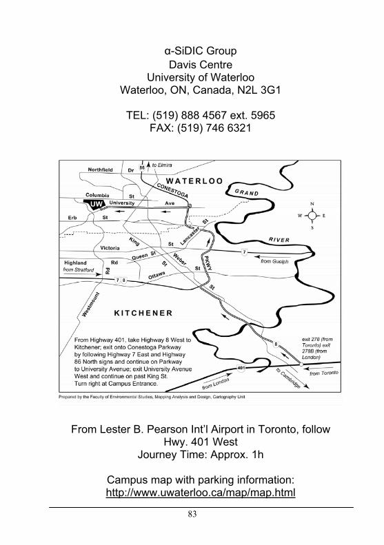
83
α-SiDIC Group Davis Centre
University of Waterloo Waterloo, ON, Canada, N2L 3G1
TEL: (519) 888 4567 ext. 5965
FAX: (519) 746 6321
From Lester B. Pearson Int’l Airport in Toronto, follow Hwy. 401 West
Journey Time: Approx. 1h
Campus map with parking information: http://www.uwaterloo.ca/map/map.html


![Review Article Bioactive Peptides: A Review - BASclbme.bas.bg/bioautomation/2011/vol_15.4/files/15.4_02.pdf · Review Article Bioactive Peptides: A Review ... casein [145]. Other](https://static.fdocument.org/doc/165x107/5acd360f7f8b9a93268d5e73/review-article-bioactive-peptides-a-review-article-bioactive-peptides-a-review.jpg)