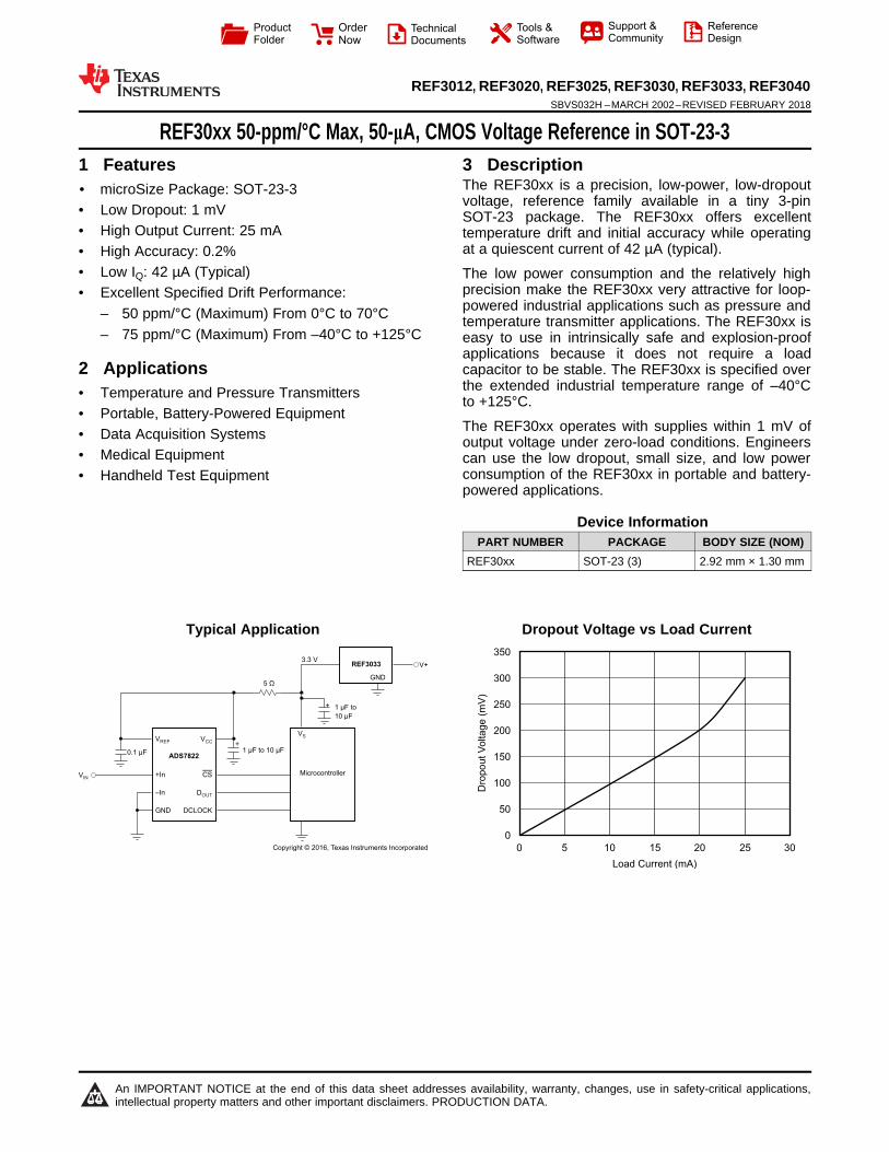
REF30xx 50-ppm/°C Max, 50-μA, CMOS Voltage Reference in ... · REF30xx 50-ppm/°C Max, 50-μA,...
29
350 300 250 200 150 100 50 0 Dropout Voltage (mV) 0 5 10 15 20 25 30 Load Current (mA) 5Ω ADS7822 V CC CS D OUT DCLOCK V REF +In –In GND + + 1 F to 10 F μ μ 1 F to μ 10 F μ 3.3 V 0.1 F μ V IN V+ V S Microcontroller REF3033 GND Copyright © 2016, Texas Instruments Incorporated Product Folder Order Now Technical Documents Tools & Software Support & Community Reference Design An IMPORTANT NOTICE at the end of this data sheet addresses availability, warranty, changes, use in safety-critical applications, intellectual property matters and other important disclaimers. PRODUCTION DATA. REF3012, REF3020, REF3025, REF3030, REF3033, REF3040 SBVS032H – MARCH 2002 – REVISED FEBRUARY 2018 REF30xx 50-ppm/°C Max, 50-μA, CMOS Voltage Reference in SOT-23-3 1 1 Features 1• microSize Package: SOT-23-3 • Low Dropout: 1 mV • High Output Current: 25 mA • High Accuracy: 0.2% • Low I Q : 42 μA (Typical) • Excellent Specified Drift Performance: – 50 ppm/°C (Maximum) From 0°C to 70°C – 75 ppm/°C (Maximum) From –40°C to +125°C 2 Applications • Temperature and Pressure Transmitters • Portable, Battery-Powered Equipment • Data Acquisition Systems • Medical Equipment • Handheld Test Equipment 3 Description The REF30xx is a precision, low-power, low-dropout voltage, reference family available in a tiny 3-pin SOT-23 package. The REF30xx offers excellent temperature drift and initial accuracy while operating at a quiescent current of 42 μA (typical). The low power consumption and the relatively high precision make the REF30xx very attractive for loop- powered industrial applications such as pressure and temperature transmitter applications. The REF30xx is easy to use in intrinsically safe and explosion-proof applications because it does not require a load capacitor to be stable. The REF30xx is specified over the extended industrial temperature range of –40°C to +125°C. The REF30xx operates with supplies within 1 mV of output voltage under zero-load conditions. Engineers can use the low dropout, small size, and low power consumption of the REF30xx in portable and battery- powered applications. Device Information PART NUMBER PACKAGE BODY SIZE (NOM) REF30xx SOT-23 (3) 2.92 mm × 1.30 mm Typical Application Dropout Voltage vs Load Current
Transcript of REF30xx 50-ppm/°C Max, 50-μA, CMOS Voltage Reference in ... · REF30xx 50-ppm/°C Max, 50-μA,...
350
300
250
200
150
100
50
0
Dro
pout V
oltage (
mV
)
0 5 10 15 20 25 30
Load Current (mA)
5 Ω
ADS7822
VCC
CS
DOUT
DCLOCK
VREF
+In
–In
GND
+
+
1 F to 10 Fμ μ
1 F toμ
10 Fμ
3.3 V
0.1 Fμ
VIN
V+
VS
Microcontroller
REF3033
GND
Copyright © 2016, Texas Instruments Incorporated
Product
Folder
Order
Now
Technical
Documents
Tools &
Software
Support &Community
ReferenceDesign
An IMPORTANT NOTICE at the end of this data sheet addresses availability, warranty, changes, use in safety-critical applications,intellectual property matters and other important disclaimers. PRODUCTION DATA.
REF3012, REF3020, REF3025, REF3030, REF3033, REF3040SBVS032H –MARCH 2002–REVISED FEBRUARY 2018
REF30xx 50-ppm/°C Max, 50-μA, CMOS Voltage Reference in SOT-23-3
1
1 Features1• microSize Package: SOT-23-3• Low Dropout: 1 mV• High Output Current: 25 mA• High Accuracy: 0.2%• Low IQ: 42 µA (Typical)• Excellent Specified Drift Performance:
– 50 ppm/°C (Maximum) From 0°C to 70°C– 75 ppm/°C (Maximum) From –40°C to +125°C
2 Applications• Temperature and Pressure Transmitters• Portable, Battery-Powered Equipment• Data Acquisition Systems• Medical Equipment• Handheld Test Equipment
3 DescriptionThe REF30xx is a precision, low-power, low-dropoutvoltage, reference family available in a tiny 3-pinSOT-23 package. The REF30xx offers excellenttemperature drift and initial accuracy while operatingat a quiescent current of 42 µA (typical).
The low power consumption and the relatively highprecision make the REF30xx very attractive for loop-powered industrial applications such as pressure andtemperature transmitter applications. The REF30xx iseasy to use in intrinsically safe and explosion-proofapplications because it does not require a loadcapacitor to be stable. The REF30xx is specified overthe extended industrial temperature range of –40°Cto +125°C.
The REF30xx operates with supplies within 1 mV ofoutput voltage under zero-load conditions. Engineerscan use the low dropout, small size, and low powerconsumption of the REF30xx in portable and battery-powered applications.
Device InformationPART NUMBER PACKAGE BODY SIZE (NOM)
REF30xx SOT-23 (3) 2.92 mm × 1.30 mm
Typical Application Dropout Voltage vs Load Current
2
REF3012, REF3020, REF3025, REF3030, REF3033, REF3040SBVS032H –MARCH 2002–REVISED FEBRUARY 2018 www.ti.com
Product Folder Links: REF3012 REF3020 REF3025 REF3030 REF3033 REF3040
Submit Documentation Feedback Copyright © 2002–2018, Texas Instruments Incorporated
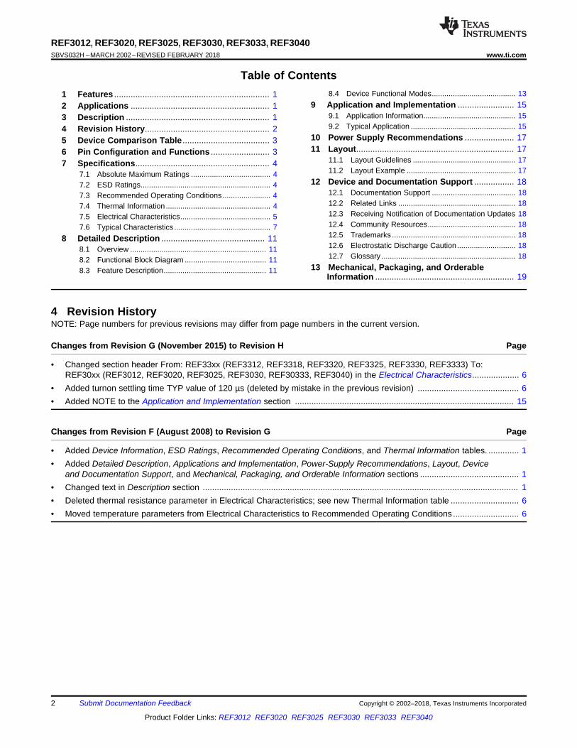
Table of Contents1 Features .................................................................. 12 Applications ........................................................... 13 Description ............................................................. 14 Revision History..................................................... 25 Device Comparison Table ..................................... 36 Pin Configuration and Functions ......................... 37 Specifications......................................................... 4
7.1 Absolute Maximum Ratings ...................................... 47.2 ESD Ratings.............................................................. 47.3 Recommended Operating Conditions....................... 47.4 Thermal Information .................................................. 47.5 Electrical Characteristics........................................... 57.6 Typical Characteristics .............................................. 7
8 Detailed Description ............................................ 118.1 Overview ................................................................. 118.2 Functional Block Diagram ....................................... 118.3 Feature Description................................................. 11
8.4 Device Functional Modes........................................ 139 Application and Implementation ........................ 15
9.1 Application Information............................................ 159.2 Typical Application .................................................. 15
10 Power Supply Recommendations ..................... 1711 Layout................................................................... 17
11.1 Layout Guidelines ................................................. 1711.2 Layout Example .................................................... 17
12 Device and Documentation Support ................. 1812.1 Documentation Support ........................................ 1812.2 Related Links ........................................................ 1812.3 Receiving Notification of Documentation Updates 1812.4 Community Resources.......................................... 1812.5 Trademarks ........................................................... 1812.6 Electrostatic Discharge Caution............................ 1812.7 Glossary ................................................................ 18
13 Mechanical, Packaging, and OrderableInformation ........................................................... 19
4 Revision HistoryNOTE: Page numbers for previous revisions may differ from page numbers in the current version.
Changes from Revision G (November 2015) to Revision H Page
• Changed section header From: REF33xx (REF3312, REF3318, REF3320, REF3325, REF3330, REF3333) To:REF30xx (REF3012, REF3020, REF3025, REF3030, REF30333, REF3040) in the Electrical Characteristics.................... 6
• Added turnon settling time TYP value of 120 µs (deleted by mistake in the previous revision) ........................................... 6• Added NOTE to the Application and Implementation section ............................................................................................. 15
Changes from Revision F (August 2008) to Revision G Page
• Added Device Information, ESD Ratings, Recommended Operating Conditions, and Thermal Information tables. ............. 1• Added Detailed Description, Applications and Implementation, Power-Supply Recommendations, Layout, Device
and Documentation Support, and Mechanical, Packaging, and Orderable Information sections .......................................... 1• Changed text in Description section ...................................................................................................................................... 1• Deleted thermal resistance parameter in Electrical Characteristics; see new Thermal Information table ............................. 6• Moved temperature parameters from Electrical Characteristics to Recommended Operating Conditions ............................ 6
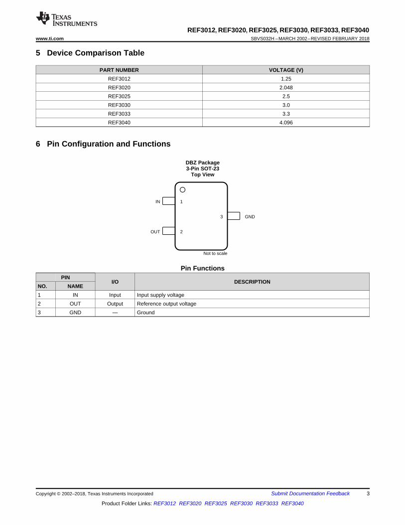
1IN
2OUT
3 GND
Not to scale
3
REF3012, REF3020, REF3025, REF3030, REF3033, REF3040www.ti.com SBVS032H –MARCH 2002–REVISED FEBRUARY 2018
Product Folder Links: REF3012 REF3020 REF3025 REF3030 REF3033 REF3040
Submit Documentation FeedbackCopyright © 2002–2018, Texas Instruments Incorporated
5 Device Comparison Table
PART NUMBER VOLTAGE (V)REF3012 1.25REF3020 2.048REF3025 2.5REF3030 3.0REF3033 3.3REF3040 4.096
6 Pin Configuration and Functions
DBZ Package3-Pin SOT-23
Top View
Pin FunctionsPIN
I/O DESCRIPTIONNO. NAME1 IN Input Input supply voltage2 OUT Output Reference output voltage3 GND — Ground
4
REF3012, REF3020, REF3025, REF3030, REF3033, REF3040SBVS032H –MARCH 2002–REVISED FEBRUARY 2018 www.ti.com
Product Folder Links: REF3012 REF3020 REF3025 REF3030 REF3033 REF3040
Submit Documentation Feedback Copyright © 2002–2018, Texas Instruments Incorporated
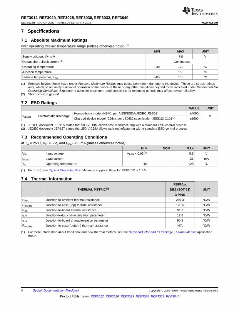
(1) Stresses beyond those listed under Absolute Maximum Ratings may cause permanent damage to the device. These are stress ratingsonly, which do not imply functional operation of the device at these or any other conditions beyond those indicated under RecommendedOperating Conditions. Exposure to absolute-maximum-rated conditions for extended periods may affect device reliability.
(2) Short circuit to ground.
7 Specifications
7.1 Absolute Maximum Ratingsover operating free-air temperature range (unless otherwise noted) (1)
MIN MAX UNITSupply voltage, V+ to V– 7.0 VOutput short-circuit current (2) ContinuousOperating temperature –40 125 °CJunction temperature 150 °CStorage temperature, Tstg –65 150 °C
(1) JEDEC document JEP155 states that 500-V HBM allows safe manufacturing with a standard ESD control process.(2) JEDEC document JEP157 states that 250-V CDM allows safe manufacturing with a standard ESD control process.
7.2 ESD RatingsVALUE UNIT
V(ESD) Electrostatic dischargeHuman-body model (HBM), per ANSI/ESDA/JEDEC JS-001 (1) ±4000
VCharged-device model (CDM), per JEDEC specification JESD22-C101 (2) ±1500
(1) For IL > 0, see Typical Characteristics. Minimum supply voltage for REF3012 is 1.8 V .
7.3 Recommended Operating Conditionsat TA = 25°C, VIN = 5 V, and ILOAD = 0 mA (unless otherwise noted)
MIN NOM MAX UNITVIN Input voltage VREF + 0.05 (1) 5.5 VILOAD Load current 25 mATA Operating temperature –40 125 °C
(1) For more information about traditional and new thermal metrics, see the Semiconductor and IC Package Thermal Metrics applicationreport.
7.4 Thermal Information
THERMAL METRIC (1)REF30xx
UNITDBZ (SOT-23)3 PINS
RθJA Junction-to-ambient thermal resistance 297.3 °C/WRθJC(top) Junction-to-case (top) thermal resistance 128.5 °C/WRθJB Junction-to-board thermal resistance 91.7 °C/WψJT Junction-to-top characterization parameter 12.8 °C/WψJB Junction-to-board characterization parameter 90.3 °C/WRθJC(bot) Junction-to-case (bottom) thermal resistance N/A °C/W
5
REF3012, REF3020, REF3025, REF3030, REF3033, REF3040www.ti.com SBVS032H –MARCH 2002–REVISED FEBRUARY 2018
Product Folder Links: REF3012 REF3020 REF3025 REF3030 REF3033 REF3040
Submit Documentation FeedbackCopyright © 2002–2018, Texas Instruments Incorporated
(1) The minimum supply voltage for the REF3012 is 1.8 V.
7.5 Electrical Characteristicsat TA = 25°C, VIN = 5 V, and ILOAD = 0 mA (unless otherwise noted)
PARAMETER TEST CONDITIONS MIN TYP MAX UNIT
REF3012 (1.25 V) (1)
VOUT Output voltage 1.2475 1.25 1.2525 V
Initial accuracy 0.2%
Output voltage noisef = 0.1 Hz to 10 Hz 14 μVPP
f = 10 Hz to 10 kHz 42 µVrms
Line regulation 1.8 V ≤ VIN ≤ 5.5 V 60 190 µV/V
REF3020 (2.048 V)
VOUT Output voltage 2.044 2.048 2.052 V
Initial accuracy 0.2%
Output voltage noisef = 0.1 Hz to 10 Hz 23 μVPP
f = 10 Hz to 10 kHz 65 µVrms
Line regulation VREF + 50 mV ≤ VIN ≤ 5.5 V 110 290 µV/V
REF3025 (2.5 V)
VOUT Output voltage 2.495 2.50 2.505 V
Initial accuracy 0.2%
Output voltage noisef = 0.1 Hz to 10 Hz 28 μVPP
f = 10 Hz to 10 kHz 80 µVrms
Line regulation VREF + 50 mV ≤ VIN ≤ 5.5 V 120 325 µV/V
REF3030 (3.0 V)
VOUT Output voltage 2.994 3.0 3.006 V
Initial accuracy 0.2%
Output voltage noisef = 0.1 Hz to 10 Hz 33 μVPP
f = 10 Hz to 10 kHz 94 µVrms
Line regulation VREF + 50 mV ≤ VIN ≤ 5.5 V 120 375 µV/V
REF3033 (3.3 V)
VOUT Output voltage 3.294 3.30 3.306 V
Initial accuracy 0.2%
Output voltage noisef = 0.1 Hz to 10 Hz 36 μVPP
f = 10 Hz to 10 kHz 105 µVrms
Line regulation VREF + 50 mV ≤ VIN ≤ 5.5 V 130 400 µV/V
REF3040 (4.096 V)
VOUT Output voltage 4.088 4.096 4.104 V
Initial accuracy 0.2%
Output voltage noisef = 0.1 Hz to 10 Hz 45 μVPP
f = 10 Hz to 10 kHz 128 µVrms
Line regulation VREF + 50 mV ≤ VIN ≤ 5.5 V 160 410 µV/V
6
REF3012, REF3020, REF3025, REF3030, REF3033, REF3040SBVS032H –MARCH 2002–REVISED FEBRUARY 2018 www.ti.com
Product Folder Links: REF3012 REF3020 REF3025 REF3030 REF3033 REF3040
Submit Documentation Feedback Copyright © 2002–2018, Texas Instruments Incorporated
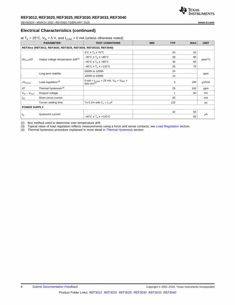
Electrical Characteristics (continued)at TA = 25°C, VIN = 5 V, and ILOAD = 0 mA (unless otherwise noted)
PARAMETER TEST CONDITIONS MIN TYP MAX UNIT
(2) Box method used to determine over temperature drift.(3) Typical value of load regulation reflects measurements using a force and sense contacts; see Load Regulation section.(4) Thermal hysteresis procedure explained in more detail in Thermal Hysteresis section.
REF30xx (REF3012, REF3020, REF3025, REF3030, REF30333, REF3040)
dVOUT/dT Output voltage temperature drift (2)
0°C ≤ TA ≤ 70°C 20 50
ppm/°C–30°C ≤ TA ≤ +85°C 28 60
–40°C ≤ TA ≤ +85°C 30 65
–40°C ≤ TA ≤ +125°C 35 75
Long-term stability0000h to 1000h 24
ppm1000h to 2000h 15
ΔVO(ΔIL) Load regulation (3) 0 mA < ILOAD < 25 mA, VIN = VREF +500 mV (1) 3 100 µV/mA
dT Thermal hysteresis (4) 25 100 ppm
VIN – VOUT Dropout voltage 1 50 mV
ISC Short-circuit current 45 mA
Turnon settling time To 0.1% with CL = 1 μF 120 µs
POWER SUPPLY
IQ Quiescent current42 50
μA–40°C ≤ TA ≤ +125°C 59
6
5
4
3
2
1
0
Load R
egula
tion (
V/m
A)
μ
Temperature (°C)
-40 -20 0 20 6040 80 100 120 140
60
50
40
30
20
10
0
I(
A)
μQ
Temperature (°C)
-40 -20 0 20 6040 80 100 120 140
2.502
2.500
2.498
2.496
2.494
2.492
2.490
Outp
ut V
oltage (
V)
-40 -20 0 20 6040 80 100 120 140
Temperature (°C)
35
30
25
20
15
10
5
Maxim
um
Load C
urr
ent (m
A)
-40 -20 0 20 6040 80 100 120 140
Temperature (°C)
50
45
40
35
30
25
20
15
10
5
0
Nu
mb
er
of
Un
its
5 10 15 20 25 30 4035 45 50 55 6560
Drift (ppm/°C)
100
90
80
70
60
50
40
30
20
10
0
Nu
mb
er
of
Un
its
5 10 15 20 25 30 4035 45 50 55 6560
Drift (ppm/°C)
7
REF3012, REF3020, REF3025, REF3030, REF3033, REF3040www.ti.com SBVS032H –MARCH 2002–REVISED FEBRUARY 2018
Product Folder Links: REF3012 REF3020 REF3025 REF3030 REF3033 REF3040
Submit Documentation FeedbackCopyright © 2002–2018, Texas Instruments Incorporated
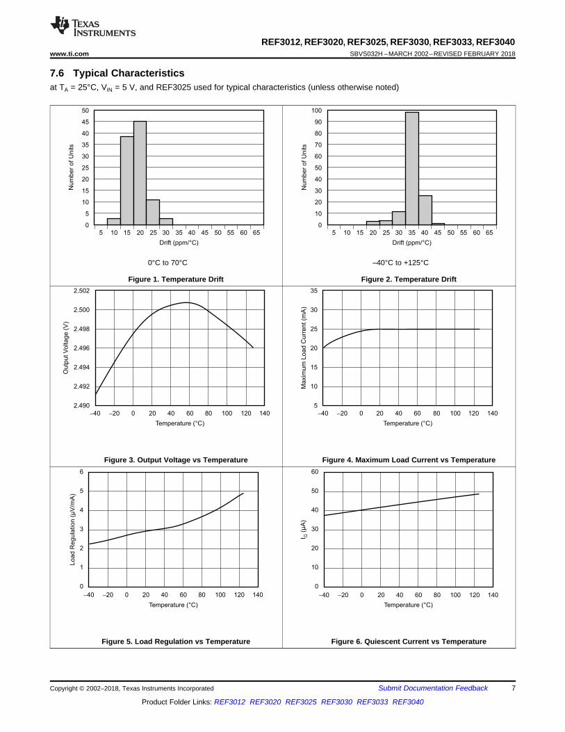
7.6 Typical Characteristicsat TA = 25°C, VIN = 5 V, and REF3025 used for typical characteristics (unless otherwise noted)
0°C to 70°C
Figure 1. Temperature Drift
–40°C to +125°C
Figure 2. Temperature Drift
Figure 3. Output Voltage vs Temperature Figure 4. Maximum Load Current vs Temperature
Figure 5. Load Regulation vs Temperature Figure 6. Quiescent Current vs Temperature
2.500200
2.500100
2.500000
2.499900
2.499800
2.499700
2.499600
2.499500
2.499400
2.499300
Ou
tpu
t V
olta
ge
(V
)
2.5 3 3.5 4 4.5 5 5.5 6
Supply (V)
2.500010
2.500000
2.499990
2.499980
2.499970
2.499960
2.499950
2.499940
2.499930
Ou
tpu
t V
olta
ge
(V
)
0 5 10 15 20 25 30
Load Current (mA)
90
80
70
60
50
40
30
20
10
0
PS
RR
(dB
)
1 10 100 1k 10k 100k
Frequency (Hz)
2.500010
2.500000
2.499990
2.499980
2.499970
2.499960
2.499950
2.499940
2.499930
2.499920
Ou
tpu
t V
olta
ge
(V
)
2.5 3 3.5 4 4.5 5 5.5 6
Supply (V)
200
150
100
50
0
-50
Lin
e R
egula
tion (
V/V
)μ
Temperature (°C)
-40 -20 0 20 6040 80 100 120 140
100
10
1
0.1
0.01
Ou
tput Im
pe
dan
ce
(dB
)
1 10 100 1k 10k 100k
Frequency (Hz)
8
REF3012, REF3020, REF3025, REF3030, REF3033, REF3040SBVS032H –MARCH 2002–REVISED FEBRUARY 2018 www.ti.com
Product Folder Links: REF3012 REF3020 REF3025 REF3030 REF3033 REF3040
Submit Documentation Feedback Copyright © 2002–2018, Texas Instruments Incorporated
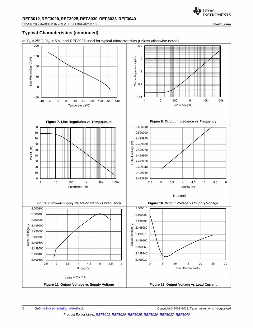
Typical Characteristics (continued)at TA = 25°C, VIN = 5 V, and REF3025 used for typical characteristics (unless otherwise noted)
Figure 7. Line Regulation vs Temperature Figure 8. Output Impedance vs Frequency
Figure 9. Power-Supply Rejection Ratio vs Frequency
No Load
Figure 10. Output Voltage vs Supply Voltage
ILOAD = 25 mA
Figure 11. Output Voltage vs Supply Voltage Figure 12. Output Voltage vs Load Current
10 ms/div
20 m
V/d
iv
I = 5 mAL
VOUT
I = 0 mAL
40 ms/div
20
mV
/div
VOUT
I = 0 mAL
I = 6 mAL
10 ms/div
50
0 m
V/d
iv5
0 m
V/d
iv
VIN
VOUT
10 ms/div
20 m
V/d
iv
I = 1 mAL
VOUT
I = 0 mAL
40 ms/div
VIN
VOUT
3 V
/div
1 V
/div
10 s/divm
VIN
5 V
/div
1 V
/div
VOUT
9
REF3012, REF3020, REF3025, REF3030, REF3033, REF3040www.ti.com SBVS032H –MARCH 2002–REVISED FEBRUARY 2018
Product Folder Links: REF3012 REF3020 REF3025 REF3030 REF3033 REF3040
Submit Documentation FeedbackCopyright © 2002–2018, Texas Instruments Incorporated
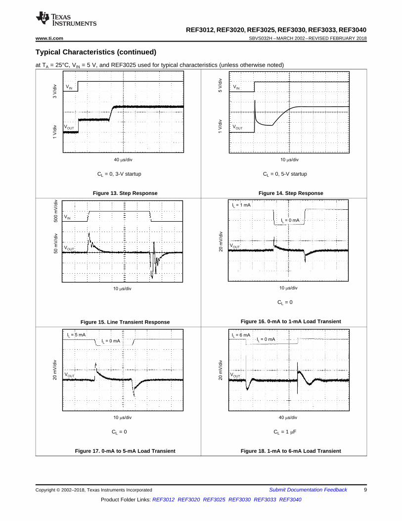
Typical Characteristics (continued)at TA = 25°C, VIN = 5 V, and REF3025 used for typical characteristics (unless otherwise noted)
CL = 0, 3-V startup
Figure 13. Step Response
CL = 0, 5-V startup
Figure 14. Step Response
Figure 15. Line Transient Response
CL = 0
Figure 16. 0-mA to 1-mA Load Transient
CL = 0
Figure 17. 0-mA to 5-mA Load Transient
CL = 1 μF
Figure 18. 1-mA to 6-mA Load Transient
Absolu
te O
utp
ut V
oltage D
rift (
ppm
)
0 200 400 600 800 1000 1200 1400 1600 1800 2000
Time (hours)
80
70
60
50
40
30
20
10
0
80
70
60
50
40
30
20
10
0
Absolu
te O
utp
ut V
oltage D
rift (
ppm
)
0 100 200 300 400 500 600 700 800 900 1000
Time (hours)
Ab
so
lute
Ou
tpu
t V
olta
ge
Drift
(p
pm
)
1200 1300 1600 1800 1900 2000
Time (hours)
80
70
60
50
40
30
20
10
0
1000 1100 1400 1500 1700
100 s/divm
20 m
V/d
iv
VOUT
I = 1 mAL
I = 25 mAL
10
mV
/div
1.0 s/div
10
REF3012, REF3020, REF3025, REF3030, REF3033, REF3040SBVS032H –MARCH 2002–REVISED FEBRUARY 2018 www.ti.com
Product Folder Links: REF3012 REF3020 REF3025 REF3030 REF3033 REF3040
Submit Documentation Feedback Copyright © 2002–2018, Texas Instruments Incorporated
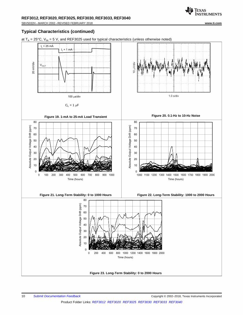
Typical Characteristics (continued)at TA = 25°C, VIN = 5 V, and REF3025 used for typical characteristics (unless otherwise noted)
CL = 1 μF
Figure 19. 1-mA to 25-mA Load Transient Figure 20. 0.1-Hz to 10-Hz Noise
Figure 21. Long-Term Stability: 0 to 1000 Hours Figure 22. Long-Term Stability: 1000 to 2000 Hours
Figure 23. Long-Term Stability: 0 to 2000 Hours
R1
Q2Q1
+
Vbe1
+
Vbe2
Copyright © 2016, Texas Instruments Incorporated
11
REF3012, REF3020, REF3025, REF3030, REF3033, REF3040www.ti.com SBVS032H –MARCH 2002–REVISED FEBRUARY 2018
Product Folder Links: REF3012 REF3020 REF3025 REF3030 REF3033 REF3040
Submit Documentation FeedbackCopyright © 2002–2018, Texas Instruments Incorporated
8 Detailed Description
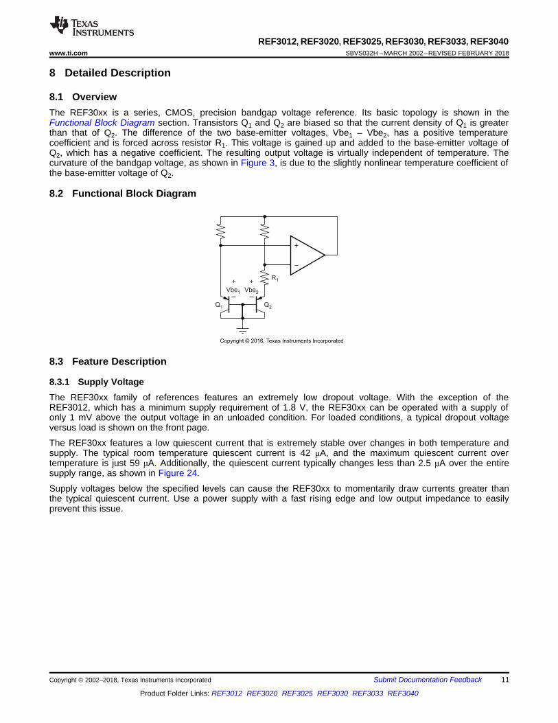
8.1 OverviewThe REF30xx is a series, CMOS, precision bandgap voltage reference. Its basic topology is shown in theFunctional Block Diagram section. Transistors Q1 and Q2 are biased so that the current density of Q1 is greaterthan that of Q2. The difference of the two base-emitter voltages, Vbe1 – Vbe2, has a positive temperaturecoefficient and is forced across resistor R1. This voltage is gained up and added to the base-emitter voltage ofQ2, which has a negative coefficient. The resulting output voltage is virtually independent of temperature. Thecurvature of the bandgap voltage, as shown in Figure 3, is due to the slightly nonlinear temperature coefficient ofthe base-emitter voltage of Q2.
8.2 Functional Block Diagram
8.3 Feature Description
8.3.1 Supply VoltageThe REF30xx family of references features an extremely low dropout voltage. With the exception of theREF3012, which has a minimum supply requirement of 1.8 V, the REF30xx can be operated with a supply ofonly 1 mV above the output voltage in an unloaded condition. For loaded conditions, a typical dropout voltageversus load is shown on the front page.
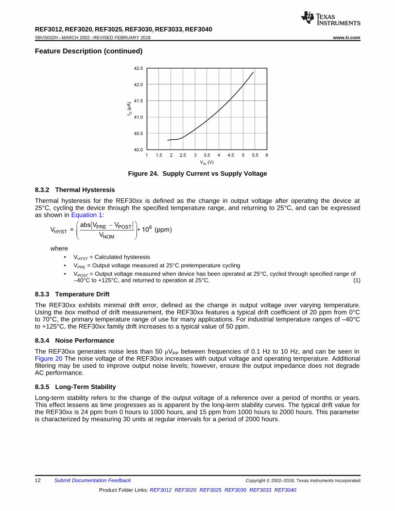
The REF30xx features a low quiescent current that is extremely stable over changes in both temperature andsupply. The typical room temperature quiescent current is 42 μA, and the maximum quiescent current overtemperature is just 59 μA. Additionally, the quiescent current typically changes less than 2.5 μA over the entiresupply range, as shown in Figure 24.
Supply voltages below the specified levels can cause the REF30xx to momentarily draw currents greater thanthe typical quiescent current. Use a power supply with a fast rising edge and low output impedance to easilyprevent this issue.
PRE POST 6HYST
NOM
abs V VV = • 10 (ppm)
V
æ ö-ç ÷ç ÷è ø
42.5
42.0
41.5
41.0
40.5
40.0
I(
A)
μQ
1 1.5 2 2.5 3 3.5 4 4.5 5 5.5 6
V (V)IN
12
REF3012, REF3020, REF3025, REF3030, REF3033, REF3040SBVS032H –MARCH 2002–REVISED FEBRUARY 2018 www.ti.com
Product Folder Links: REF3012 REF3020 REF3025 REF3030 REF3033 REF3040
Submit Documentation Feedback Copyright © 2002–2018, Texas Instruments Incorporated
Feature Description (continued)
Figure 24. Supply Current vs Supply Voltage
8.3.2 Thermal HysteresisThermal hysteresis for the REF30xx is defined as the change in output voltage after operating the device at25°C, cycling the device through the specified temperature range, and returning to 25°C, and can be expressedas shown in Equation 1:
where• VHYST = Calculated hysteresis• VPRE = Output voltage measured at 25°C pretemperature cycling• VPOST = Output voltage measured when device has been operated at 25°C, cycled through specified range of
–40°C to +125°C, and returned to operation at 25°C. (1)
8.3.3 Temperature DriftThe REF30xx exhibits minimal drift error, defined as the change in output voltage over varying temperature.Using the box method of drift measurement, the REF30xx features a typical drift coefficient of 20 ppm from 0°Cto 70°C, the primary temperature range of use for many applications. For industrial temperature ranges of –40°Cto +125°C, the REF30xx family drift increases to a typical value of 50 ppm.
8.3.4 Noise PerformanceThe REF30xx generates noise less than 50 μVPP between frequencies of 0.1 Hz to 10 Hz, and can be seen inFigure 20 The noise voltage of the REF30xx increases with output voltage and operating temperature. Additionalfiltering may be used to improve output noise levels; however, ensure the output impedance does not degradeAC performance.
8.3.5 Long-Term StabilityLong-term stability refers to the change of the output voltage of a reference over a period of months or years.This effect lessens as time progresses as is apparent by the long-term stability curves. The typical drift value forthe REF30xx is 24 ppm from 0 hours to 1000 hours, and 15 ppm from 1000 hours to 2000 hours. This parameteris characterized by measuring 30 units at regular intervals for a period of 2000 hours.
OPA703
REF3025
+5 V
-5 V
+5V
10 kW
10 kW
+2.5 V
-2.5 V
Copyright © 2016, Texas Instruments Incorporated
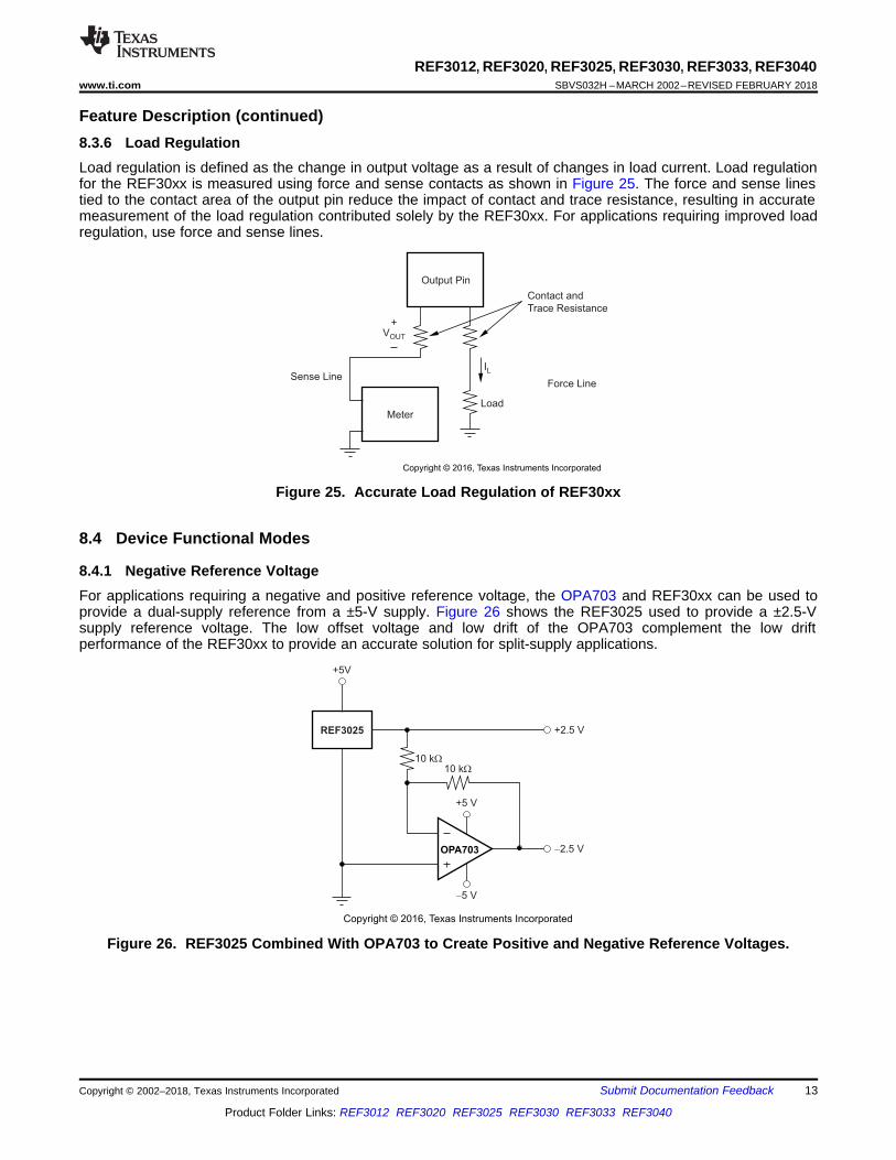
Output Pin
Meter
VOUT
+
Sense LineForce Line
Load
IL
Contact and
Trace Resistance
Copyright © 2016, Texas Instruments Incorporated
13
REF3012, REF3020, REF3025, REF3030, REF3033, REF3040www.ti.com SBVS032H –MARCH 2002–REVISED FEBRUARY 2018
Product Folder Links: REF3012 REF3020 REF3025 REF3030 REF3033 REF3040
Submit Documentation FeedbackCopyright © 2002–2018, Texas Instruments Incorporated
Feature Description (continued)8.3.6 Load RegulationLoad regulation is defined as the change in output voltage as a result of changes in load current. Load regulationfor the REF30xx is measured using force and sense contacts as shown in Figure 25. The force and sense linestied to the contact area of the output pin reduce the impact of contact and trace resistance, resulting in accuratemeasurement of the load regulation contributed solely by the REF30xx. For applications requiring improved loadregulation, use force and sense lines.
Figure 25. Accurate Load Regulation of REF30xx
8.4 Device Functional Modes
8.4.1 Negative Reference VoltageFor applications requiring a negative and positive reference voltage, the OPA703 and REF30xx can be used toprovide a dual-supply reference from a ±5-V supply. Figure 26 shows the REF3025 used to provide a ±2.5-Vsupply reference voltage. The low offset voltage and low drift of the OPA703 complement the low driftperformance of the REF30xx to provide an accurate solution for split-supply applications.
Figure 26. REF3025 Combined With OPA703 to Create Positive and Negative Reference Voltages.
ADS8324
VCC
CS
DOUT
DCLOCK
VREF
+In
–In
GND
+
+
5 Ω
1 F to 10 Fμ μ
1 F to 10 Fμ μ
0.1 Fμ
0 V to 1.25 V Microcontroller
2.5-V Supply
REF3012
GND
VIN
VOUT
2.5 V
1.25 V VS
Copyright © 2016, Texas Instruments Incorporated
5 Ω
ADS7822
VCC
CS
DOUT
DCLOCK
VREF
+In
–In
GND
+
+
1 F to 10 Fμ μ
1 F toμ
10 Fμ
3.3 V
0.1 Fμ
VIN
V+
VS
Microcontroller
REF3033
GND
Copyright © 2016, Texas Instruments Incorporated
14
REF3012, REF3020, REF3025, REF3030, REF3033, REF3040SBVS032H –MARCH 2002–REVISED FEBRUARY 2018 www.ti.com
Product Folder Links: REF3012 REF3020 REF3025 REF3030 REF3033 REF3040
Submit Documentation Feedback Copyright © 2002–2018, Texas Instruments Incorporated
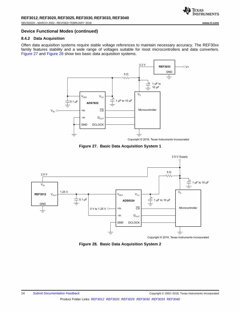
Device Functional Modes (continued)8.4.2 Data AcquisitionOften data acquisition systems require stable voltage references to maintain necessary accuracy. The REF30xxfamily features stability and a wide range of voltages suitable for most microcontrollers and data converters.Figure 27 and Figure 28 show two basic data acquisition systems.
Figure 27. Basic Data Acquisition System 1
Figure 28. Basic Data Acquisition System 2
+
+±
+
±
IN OUT
REF3012
IN OUT
REF30303.3 V
R2
R1
1.25 V
20 k
R3
3.0 V VOUT
20 k
OPA317
100 k
10 k
3.0 V 1.25 V
3.3 V
IN+
IN±
SD_16
VR
EF
J1.2/A1+
J1.3/A1±
J1.5/VREF
0.625 V
C2
47 µF
R6
47 k
R7
47 k
VIN
±5 V
R4
�A-ADC
R5
3.0 V
MSP430F2013 Launchpad
100 k
Copyright © 2016, Texas Instruments Incorporated
1
3REF30xx
2
0.47 Fm
VIN
VOUT
Copyright © 2016, Texas Instruments Incorporated
15
REF3012, REF3020, REF3025, REF3030, REF3033, REF3040www.ti.com SBVS032H –MARCH 2002–REVISED FEBRUARY 2018
Product Folder Links: REF3012 REF3020 REF3025 REF3030 REF3033 REF3040
Submit Documentation FeedbackCopyright © 2002–2018, Texas Instruments Incorporated
9 Application and Implementation
NOTEInformation in the following applications sections is not part of the TI componentspecification, and TI does not warrant its accuracy or completeness. TI’s customers areresponsible for determining suitability of components for their purposes. Customers shouldvalidate and test their design implementation to confirm system functionality.
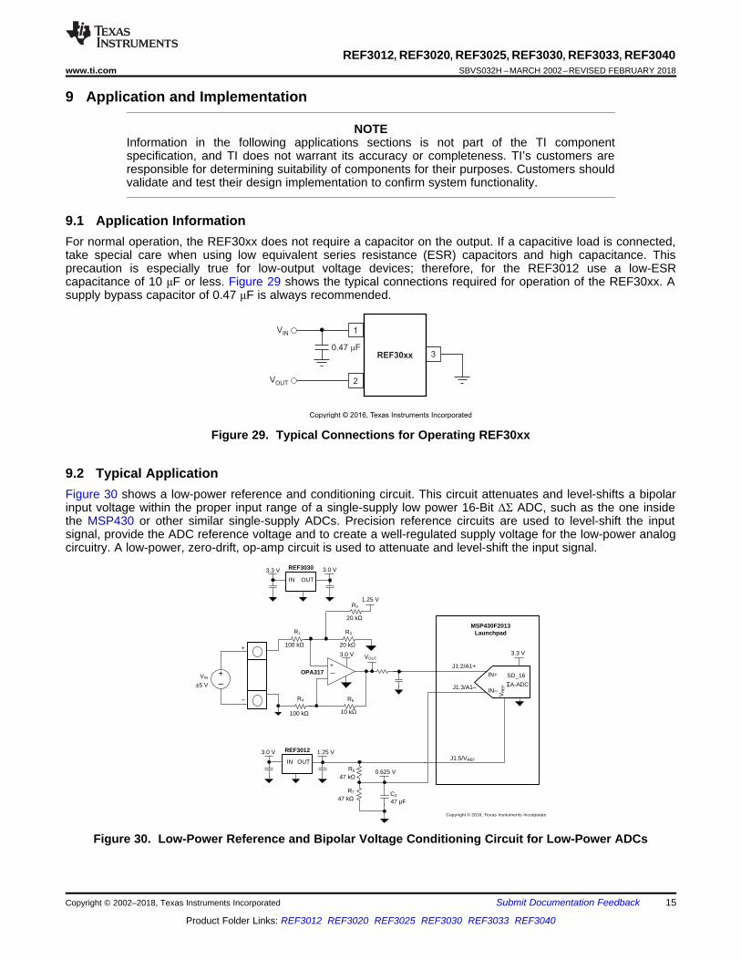
9.1 Application InformationFor normal operation, the REF30xx does not require a capacitor on the output. If a capacitive load is connected,take special care when using low equivalent series resistance (ESR) capacitors and high capacitance. Thisprecaution is especially true for low-output voltage devices; therefore, for the REF3012 use a low-ESRcapacitance of 10 μF or less. Figure 29 shows the typical connections required for operation of the REF30xx. Asupply bypass capacitor of 0.47 μF is always recommended.
Figure 29. Typical Connections for Operating REF30xx
9.2 Typical ApplicationFigure 30 shows a low-power reference and conditioning circuit. This circuit attenuates and level-shifts a bipolarinput voltage within the proper input range of a single-supply low power 16-Bit ΔΣ ADC, such as the one insidethe MSP430 or other similar single-supply ADCs. Precision reference circuits are used to level-shift the inputsignal, provide the ADC reference voltage and to create a well-regulated supply voltage for the low-power analogcircuitry. A low-power, zero-drift, op-amp circuit is used to attenuate and level-shift the input signal.
Figure 30. Low-Power Reference and Bipolar Voltage Conditioning Circuit for Low-Power ADCs
±200
±150
±100
±50
0
50
100
150
±6 ±5 ±4 ±3 ±2 ±1 0 1 2 3 4 5 6
Out
put C
ode
Err
or (
# of
cod
es)
Input Voltage (V) C003
0
0.25
0.5
0.75
1
1.25
±6 ±5 ±4 ±3 ±2 ±1 0 1 2 3 4 5 6
Out
put V
olta
ge (
V)
Input Voltage (V) C001
-0.00035
-0.0003
-0.00025
-0.0002
-0.00015
-0.0001
±6 ±5 ±4 ±3 ±2 ±1 0 1 2 3 4 5 6
Err
or V
olta
ge (
V)
Input Voltage (V) C00
16
REF3012, REF3020, REF3025, REF3030, REF3033, REF3040SBVS032H –MARCH 2002–REVISED FEBRUARY 2018 www.ti.com
Product Folder Links: REF3012 REF3020 REF3025 REF3030 REF3033 REF3040
Submit Documentation Feedback Copyright © 2002–2018, Texas Instruments Incorporated
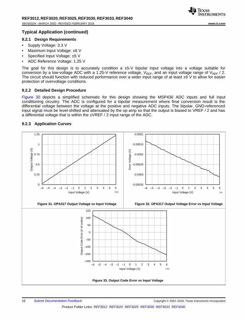
Typical Application (continued)9.2.1 Design Requirements• Supply Voltage: 3.3 V• Maximum Input Voltage: ±6 V• Specified Input Voltage: ±5 V• ADC Reference Voltage: 1.25 V
The goal for this design is to accurately condition a ±5-V bipolar input voltage into a voltage suitable forconversion by a low-voltage ADC with a 1.25-V reference voltage, VREF, and an input voltage range of VREF / 2.The circuit should function with reduced performance over a wider input range of at least ±6 V to allow for easierprotection of overvoltage conditions.
9.2.2 Detailed Design ProcedureFigure 30 depicts a simplified schematic for this design showing the MSP430 ADC inputs and full inputconditioning circuitry. The ADC is configured for a bipolar measurement where final conversion result is thedifferential voltage between the voltage at the positive and negative ADC inputs. The bipolar, GND-referencedinput signal must be level-shifted and attenuated by the op amp so that the output is biased to VREF / 2 and hasa differential voltage that is within the ±VREF / 2 input range of the ADC.
9.2.3 Application Curves
Figure 31. OPA317 Output Voltage vs Input Voltage Figure 32. OPA317 Output Voltage Error vs Input Voltage
Figure 33. Output Code Error vs Input Voltage
OUT
GND
IN
C C
REF30xx
To ADC To Input Power Supply
Via to Ground Plane
17
REF3012, REF3020, REF3025, REF3030, REF3033, REF3040www.ti.com SBVS032H –MARCH 2002–REVISED FEBRUARY 2018
Product Folder Links: REF3012 REF3020 REF3025 REF3030 REF3033 REF3040
Submit Documentation FeedbackCopyright © 2002–2018, Texas Instruments Incorporated
10 Power Supply RecommendationsThe REF30xx family of references feature an extremely low-dropout voltage. These references can be operatedwith a supply of only 50 mV above the output voltage. For loaded reference conditions, a typical dropout voltageversus load is shown in the front page plot, Dropout Voltage vs Load Current. Use a supply bypass capacitorgreater than 0.47 µF.
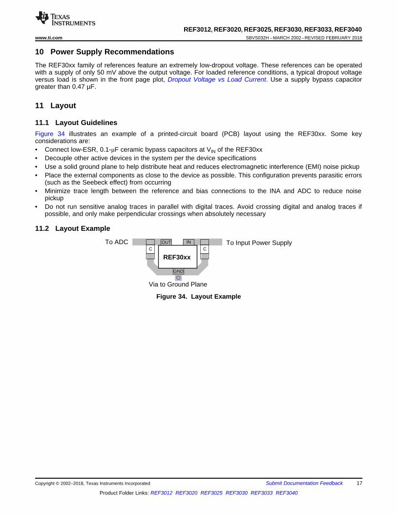
11 Layout
11.1 Layout GuidelinesFigure 34 illustrates an example of a printed-circuit board (PCB) layout using the REF30xx. Some keyconsiderations are:• Connect low-ESR, 0.1-μF ceramic bypass capacitors at VIN of the REF30xx• Decouple other active devices in the system per the device specifications• Use a solid ground plane to help distribute heat and reduces electromagnetic interference (EMI) noise pickup• Place the external components as close to the device as possible. This configuration prevents parasitic errors
(such as the Seebeck effect) from occurring• Minimize trace length between the reference and bias connections to the INA and ADC to reduce noise
pickup• Do not run sensitive analog traces in parallel with digital traces. Avoid crossing digital and analog traces if
possible, and only make perpendicular crossings when absolutely necessary
11.2 Layout Example
Figure 34. Layout Example
18
REF3012, REF3020, REF3025, REF3030, REF3033, REF3040SBVS032H –MARCH 2002–REVISED FEBRUARY 2018 www.ti.com
Product Folder Links: REF3012 REF3020 REF3025 REF3030 REF3033 REF3040
Submit Documentation Feedback Copyright © 2002–2018, Texas Instruments Incorporated
12 Device and Documentation Support
12.1 Documentation Support
12.1.1 Related DocumentationCMOS, Rail-to-Rail, I/O Operational Amplifiers (SBOS180)
REF29xx 100 ppm/°C, 50 μA in 3-Pin SOT-23 CMOS Voltage Reference (SBVS033)
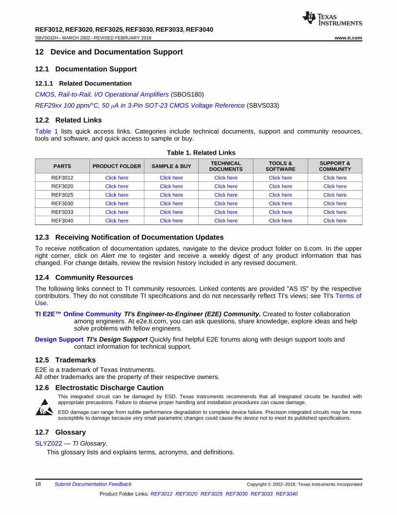
12.2 Related LinksTable 1 lists quick access links. Categories include technical documents, support and community resources,tools and software, and quick access to sample or buy.
Table 1. Related Links
PARTS PRODUCT FOLDER SAMPLE & BUY TECHNICALDOCUMENTS
TOOLS &SOFTWARE
SUPPORT &COMMUNITY
REF3012 Click here Click here Click here Click here Click hereREF3020 Click here Click here Click here Click here Click hereREF3025 Click here Click here Click here Click here Click hereREF3030 Click here Click here Click here Click here Click hereREF3033 Click here Click here Click here Click here Click hereREF3040 Click here Click here Click here Click here Click here
12.3 Receiving Notification of Documentation UpdatesTo receive notification of documentation updates, navigate to the device product folder on ti.com. In the upperright corner, click on Alert me to register and receive a weekly digest of any product information that haschanged. For change details, review the revision history included in any revised document.
12.4 Community ResourcesThe following links connect to TI community resources. Linked contents are provided "AS IS" by the respectivecontributors. They do not constitute TI specifications and do not necessarily reflect TI's views; see TI's Terms ofUse.
TI E2E™ Online Community TI's Engineer-to-Engineer (E2E) Community. Created to foster collaborationamong engineers. At e2e.ti.com, you can ask questions, share knowledge, explore ideas and helpsolve problems with fellow engineers.
Design Support TI's Design Support Quickly find helpful E2E forums along with design support tools andcontact information for technical support.
12.5 TrademarksE2E is a trademark of Texas Instruments.All other trademarks are the property of their respective owners.
12.6 Electrostatic Discharge CautionThis integrated circuit can be damaged by ESD. Texas Instruments recommends that all integrated circuits be handled withappropriate precautions. Failure to observe proper handling and installation procedures can cause damage.
ESD damage can range from subtle performance degradation to complete device failure. Precision integrated circuits may be moresusceptible to damage because very small parametric changes could cause the device not to meet its published specifications.
12.7 GlossarySLYZ022 — TI Glossary.
This glossary lists and explains terms, acronyms, and definitions.
19
REF3012, REF3020, REF3025, REF3030, REF3033, REF3040www.ti.com SBVS032H –MARCH 2002–REVISED FEBRUARY 2018
Product Folder Links: REF3012 REF3020 REF3025 REF3030 REF3033 REF3040
Submit Documentation FeedbackCopyright © 2002–2018, Texas Instruments Incorporated
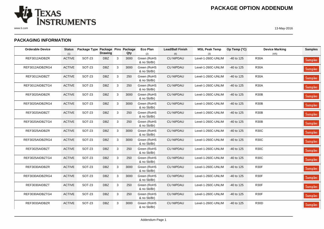
13 Mechanical, Packaging, and Orderable InformationThe following pages include mechanical packaging and orderable information. This information is the mostcurrent data available for the designated devices. This data is subject to change without notice and revision ofthis document. For browser-based versions of this data sheet, refer to the left-hand navigation.
PACKAGE OPTION ADDENDUM
www.ti.com 13-May-2016
Addendum-Page 1
PACKAGING INFORMATION
Orderable Device Status(1)
Package Type PackageDrawing
Pins PackageQty
Eco Plan(2)
Lead/Ball Finish(6)
MSL Peak Temp(3)
Op Temp (°C) Device Marking(4/5)
Samples
REF3012AIDBZR ACTIVE SOT-23 DBZ 3 3000 Green (RoHS& no Sb/Br)
CU NIPDAU Level-1-260C-UNLIM -40 to 125 R30A
REF3012AIDBZRG4 ACTIVE SOT-23 DBZ 3 3000 Green (RoHS& no Sb/Br)
CU NIPDAU Level-1-260C-UNLIM -40 to 125 R30A
REF3012AIDBZT ACTIVE SOT-23 DBZ 3 250 Green (RoHS& no Sb/Br)
CU NIPDAU Level-1-260C-UNLIM -40 to 125 R30A
REF3012AIDBZTG4 ACTIVE SOT-23 DBZ 3 250 Green (RoHS& no Sb/Br)
CU NIPDAU Level-1-260C-UNLIM -40 to 125 R30A
REF3020AIDBZR ACTIVE SOT-23 DBZ 3 3000 Green (RoHS& no Sb/Br)
CU NIPDAU Level-1-260C-UNLIM -40 to 125 R30B
REF3020AIDBZRG4 ACTIVE SOT-23 DBZ 3 3000 Green (RoHS& no Sb/Br)
CU NIPDAU Level-1-260C-UNLIM -40 to 125 R30B
REF3020AIDBZT ACTIVE SOT-23 DBZ 3 250 Green (RoHS& no Sb/Br)
CU NIPDAU Level-1-260C-UNLIM -40 to 125 R30B
REF3020AIDBZTG4 ACTIVE SOT-23 DBZ 3 250 Green (RoHS& no Sb/Br)
CU NIPDAU Level-1-260C-UNLIM -40 to 125 R30B
REF3025AIDBZR ACTIVE SOT-23 DBZ 3 3000 Green (RoHS& no Sb/Br)
CU NIPDAU Level-1-260C-UNLIM -40 to 125 R30C
REF3025AIDBZRG4 ACTIVE SOT-23 DBZ 3 3000 Green (RoHS& no Sb/Br)
CU NIPDAU Level-1-260C-UNLIM -40 to 125 R30C
REF3025AIDBZT ACTIVE SOT-23 DBZ 3 250 Green (RoHS& no Sb/Br)
CU NIPDAU Level-1-260C-UNLIM -40 to 125 R30C
REF3025AIDBZTG4 ACTIVE SOT-23 DBZ 3 250 Green (RoHS& no Sb/Br)
CU NIPDAU Level-1-260C-UNLIM -40 to 125 R30C
REF3030AIDBZR ACTIVE SOT-23 DBZ 3 3000 Green (RoHS& no Sb/Br)
CU NIPDAU Level-1-260C-UNLIM -40 to 125 R30F
REF3030AIDBZRG4 ACTIVE SOT-23 DBZ 3 3000 Green (RoHS& no Sb/Br)
CU NIPDAU Level-1-260C-UNLIM -40 to 125 R30F
REF3030AIDBZT ACTIVE SOT-23 DBZ 3 250 Green (RoHS& no Sb/Br)
CU NIPDAU Level-1-260C-UNLIM -40 to 125 R30F
REF3030AIDBZTG4 ACTIVE SOT-23 DBZ 3 250 Green (RoHS& no Sb/Br)
CU NIPDAU Level-1-260C-UNLIM -40 to 125 R30F
REF3033AIDBZR ACTIVE SOT-23 DBZ 3 3000 Green (RoHS& no Sb/Br)
CU NIPDAU Level-1-260C-UNLIM -40 to 125 R30D
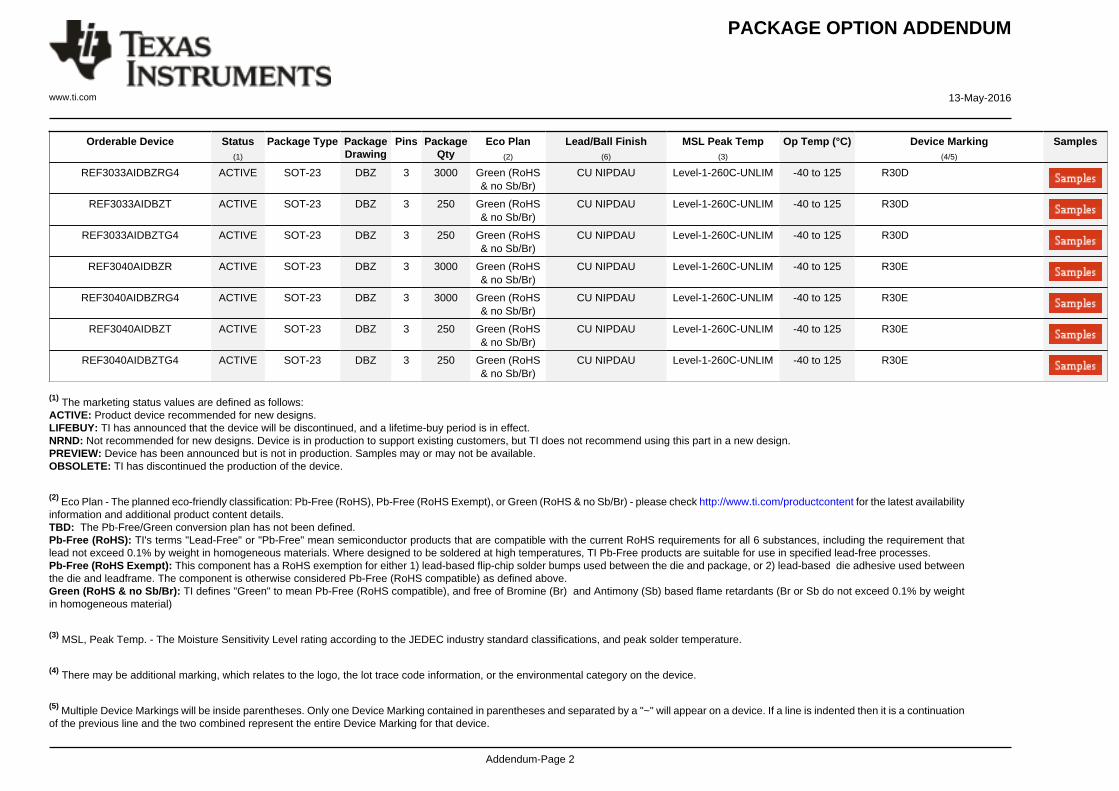
PACKAGE OPTION ADDENDUM
www.ti.com 13-May-2016
Addendum-Page 2
Orderable Device Status(1)
Package Type PackageDrawing
Pins PackageQty
Eco Plan(2)
Lead/Ball Finish(6)
MSL Peak Temp(3)
Op Temp (°C) Device Marking(4/5)
Samples
REF3033AIDBZRG4 ACTIVE SOT-23 DBZ 3 3000 Green (RoHS& no Sb/Br)
CU NIPDAU Level-1-260C-UNLIM -40 to 125 R30D
REF3033AIDBZT ACTIVE SOT-23 DBZ 3 250 Green (RoHS& no Sb/Br)
CU NIPDAU Level-1-260C-UNLIM -40 to 125 R30D
REF3033AIDBZTG4 ACTIVE SOT-23 DBZ 3 250 Green (RoHS& no Sb/Br)
CU NIPDAU Level-1-260C-UNLIM -40 to 125 R30D
REF3040AIDBZR ACTIVE SOT-23 DBZ 3 3000 Green (RoHS& no Sb/Br)
CU NIPDAU Level-1-260C-UNLIM -40 to 125 R30E
REF3040AIDBZRG4 ACTIVE SOT-23 DBZ 3 3000 Green (RoHS& no Sb/Br)
CU NIPDAU Level-1-260C-UNLIM -40 to 125 R30E
REF3040AIDBZT ACTIVE SOT-23 DBZ 3 250 Green (RoHS& no Sb/Br)
CU NIPDAU Level-1-260C-UNLIM -40 to 125 R30E
REF3040AIDBZTG4 ACTIVE SOT-23 DBZ 3 250 Green (RoHS& no Sb/Br)
CU NIPDAU Level-1-260C-UNLIM -40 to 125 R30E
(1) The marketing status values are defined as follows:ACTIVE: Product device recommended for new designs.LIFEBUY: TI has announced that the device will be discontinued, and a lifetime-buy period is in effect.NRND: Not recommended for new designs. Device is in production to support existing customers, but TI does not recommend using this part in a new design.PREVIEW: Device has been announced but is not in production. Samples may or may not be available.OBSOLETE: TI has discontinued the production of the device.
(2) Eco Plan - The planned eco-friendly classification: Pb-Free (RoHS), Pb-Free (RoHS Exempt), or Green (RoHS & no Sb/Br) - please check http://www.ti.com/productcontent for the latest availabilityinformation and additional product content details.TBD: The Pb-Free/Green conversion plan has not been defined.Pb-Free (RoHS): TI's terms "Lead-Free" or "Pb-Free" mean semiconductor products that are compatible with the current RoHS requirements for all 6 substances, including the requirement thatlead not exceed 0.1% by weight in homogeneous materials. Where designed to be soldered at high temperatures, TI Pb-Free products are suitable for use in specified lead-free processes.Pb-Free (RoHS Exempt): This component has a RoHS exemption for either 1) lead-based flip-chip solder bumps used between the die and package, or 2) lead-based die adhesive used betweenthe die and leadframe. The component is otherwise considered Pb-Free (RoHS compatible) as defined above.Green (RoHS & no Sb/Br): TI defines "Green" to mean Pb-Free (RoHS compatible), and free of Bromine (Br) and Antimony (Sb) based flame retardants (Br or Sb do not exceed 0.1% by weightin homogeneous material)
(3) MSL, Peak Temp. - The Moisture Sensitivity Level rating according to the JEDEC industry standard classifications, and peak solder temperature.
(4) There may be additional marking, which relates to the logo, the lot trace code information, or the environmental category on the device.
(5) Multiple Device Markings will be inside parentheses. Only one Device Marking contained in parentheses and separated by a "~" will appear on a device. If a line is indented then it is a continuationof the previous line and the two combined represent the entire Device Marking for that device.
PACKAGE OPTION ADDENDUM
www.ti.com 13-May-2016
Addendum-Page 3
(6) Lead/Ball Finish - Orderable Devices may have multiple material finish options. Finish options are separated by a vertical ruled line. Lead/Ball Finish values may wrap to two lines if the finishvalue exceeds the maximum column width.
Important Information and Disclaimer:The information provided on this page represents TI's knowledge and belief as of the date that it is provided. TI bases its knowledge and belief on informationprovided by third parties, and makes no representation or warranty as to the accuracy of such information. Efforts are underway to better integrate information from third parties. TI has taken andcontinues to take reasonable steps to provide representative and accurate information but may not have conducted destructive testing or chemical analysis on incoming materials and chemicals.TI and TI suppliers consider certain information to be proprietary, and thus CAS numbers and other limited information may not be available for release.
In no event shall TI's liability arising out of such information exceed the total purchase price of the TI part(s) at issue in this document sold by TI to Customer on an annual basis.
OTHER QUALIFIED VERSIONS OF REF3033 :
• Automotive: REF3033-Q1
NOTE: Qualified Version Definitions:
• Automotive - Q100 devices qualified for high-reliability automotive applications targeting zero defects
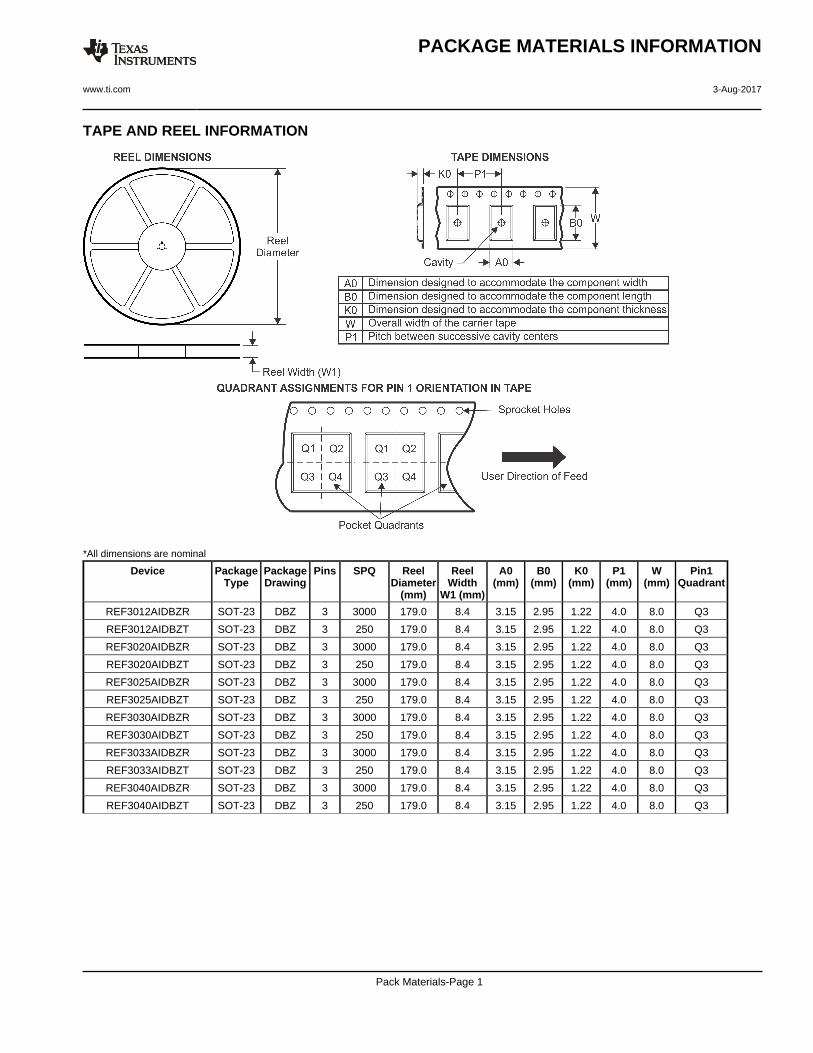
TAPE AND REEL INFORMATION
*All dimensions are nominal
Device PackageType
PackageDrawing
Pins SPQ ReelDiameter
(mm)
ReelWidth
W1 (mm)
A0(mm)
B0(mm)
K0(mm)
P1(mm)
W(mm)
Pin1Quadrant
REF3012AIDBZR SOT-23 DBZ 3 3000 179.0 8.4 3.15 2.95 1.22 4.0 8.0 Q3
REF3012AIDBZT SOT-23 DBZ 3 250 179.0 8.4 3.15 2.95 1.22 4.0 8.0 Q3
REF3020AIDBZR SOT-23 DBZ 3 3000 179.0 8.4 3.15 2.95 1.22 4.0 8.0 Q3
REF3020AIDBZT SOT-23 DBZ 3 250 179.0 8.4 3.15 2.95 1.22 4.0 8.0 Q3
REF3025AIDBZR SOT-23 DBZ 3 3000 179.0 8.4 3.15 2.95 1.22 4.0 8.0 Q3
REF3025AIDBZT SOT-23 DBZ 3 250 179.0 8.4 3.15 2.95 1.22 4.0 8.0 Q3
REF3030AIDBZR SOT-23 DBZ 3 3000 179.0 8.4 3.15 2.95 1.22 4.0 8.0 Q3
REF3030AIDBZT SOT-23 DBZ 3 250 179.0 8.4 3.15 2.95 1.22 4.0 8.0 Q3
REF3033AIDBZR SOT-23 DBZ 3 3000 179.0 8.4 3.15 2.95 1.22 4.0 8.0 Q3
REF3033AIDBZT SOT-23 DBZ 3 250 179.0 8.4 3.15 2.95 1.22 4.0 8.0 Q3
REF3040AIDBZR SOT-23 DBZ 3 3000 179.0 8.4 3.15 2.95 1.22 4.0 8.0 Q3
REF3040AIDBZT SOT-23 DBZ 3 250 179.0 8.4 3.15 2.95 1.22 4.0 8.0 Q3
PACKAGE MATERIALS INFORMATION
www.ti.com 3-Aug-2017
Pack Materials-Page 1
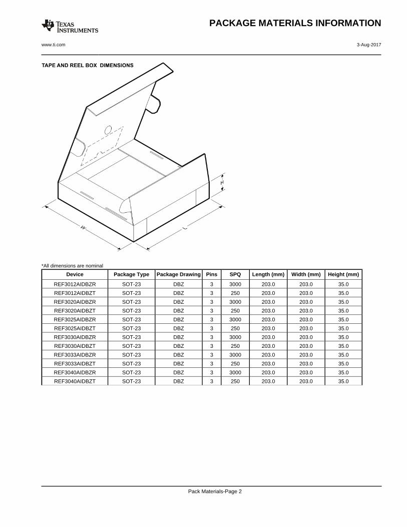
*All dimensions are nominal
Device Package Type Package Drawing Pins SPQ Length (mm) Width (mm) Height (mm)
REF3012AIDBZR SOT-23 DBZ 3 3000 203.0 203.0 35.0
REF3012AIDBZT SOT-23 DBZ 3 250 203.0 203.0 35.0
REF3020AIDBZR SOT-23 DBZ 3 3000 203.0 203.0 35.0
REF3020AIDBZT SOT-23 DBZ 3 250 203.0 203.0 35.0
REF3025AIDBZR SOT-23 DBZ 3 3000 203.0 203.0 35.0
REF3025AIDBZT SOT-23 DBZ 3 250 203.0 203.0 35.0
REF3030AIDBZR SOT-23 DBZ 3 3000 203.0 203.0 35.0
REF3030AIDBZT SOT-23 DBZ 3 250 203.0 203.0 35.0
REF3033AIDBZR SOT-23 DBZ 3 3000 203.0 203.0 35.0
REF3033AIDBZT SOT-23 DBZ 3 250 203.0 203.0 35.0
REF3040AIDBZR SOT-23 DBZ 3 3000 203.0 203.0 35.0
REF3040AIDBZT SOT-23 DBZ 3 250 203.0 203.0 35.0
PACKAGE MATERIALS INFORMATION
www.ti.com 3-Aug-2017
Pack Materials-Page 2
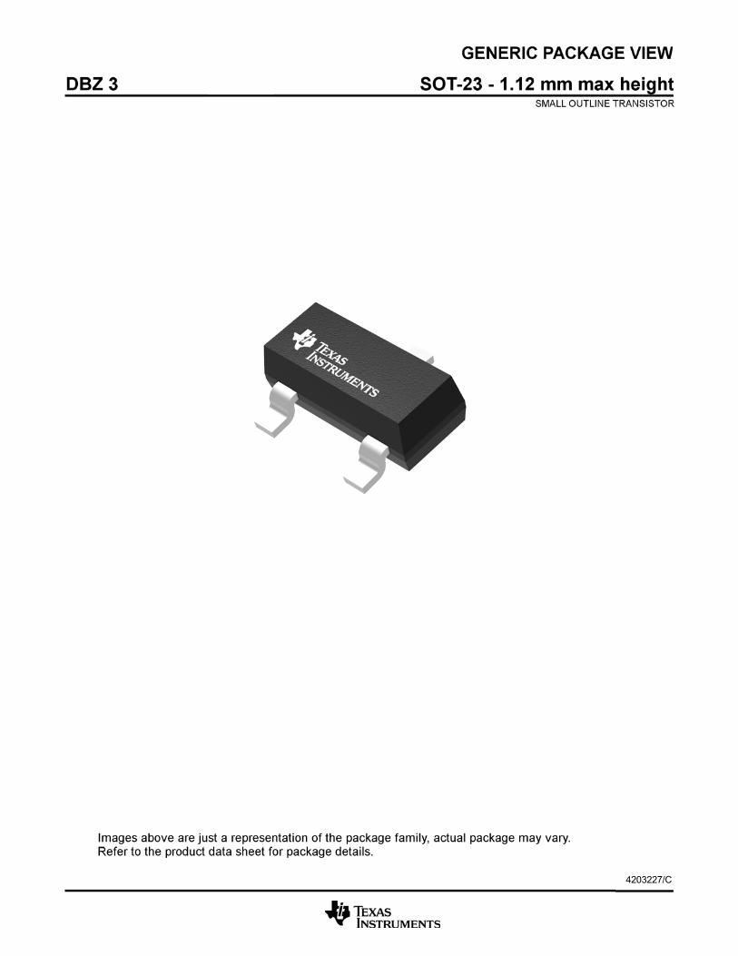
4203227/C
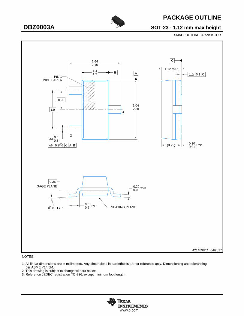
www.ti.com
PACKAGE OUTLINE
C
TYP0.200.08
0.25
2.642.10
1.12 MAX
TYP0.100.01
3X 0.50.3
TYP0.60.2
1.9
0.95
TYP-80
A
3.042.80
B1.41.2
(0.95)
SOT-23 - 1.12 mm max heightDBZ0003ASMALL OUTLINE TRANSISTOR
4214838/C 04/2017
NOTES: 1. All linear dimensions are in millimeters. Any dimensions in parenthesis are for reference only. Dimensioning and tolerancing per ASME Y14.5M.2. This drawing is subject to change without notice.3. Reference JEDEC registration TO-236, except minimum foot length.
0.2 C A B
1
3
2
INDEX AREAPIN 1
GAGE PLANE
SEATING PLANE
0.1 C
SCALE 4.000
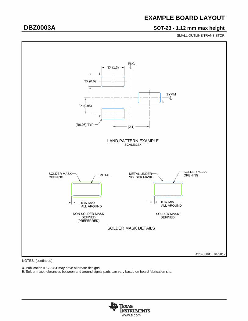
www.ti.com
EXAMPLE BOARD LAYOUT
0.07 MAXALL AROUND
0.07 MINALL AROUND
3X (1.3)
3X (0.6)
(2.1)
2X (0.95)
(R0.05) TYP
4214838/C 04/2017
SOT-23 - 1.12 mm max heightDBZ0003ASMALL OUTLINE TRANSISTOR
NOTES: (continued) 4. Publication IPC-7351 may have alternate designs. 5. Solder mask tolerances between and around signal pads can vary based on board fabrication site.
SYMM
LAND PATTERN EXAMPLESCALE:15X
PKG
1
3
2
SOLDER MASKOPENINGMETAL UNDER
SOLDER MASK
SOLDER MASKDEFINED
METALSOLDER MASKOPENING
NON SOLDER MASKDEFINED
(PREFERRED)
SOLDER MASK DETAILS
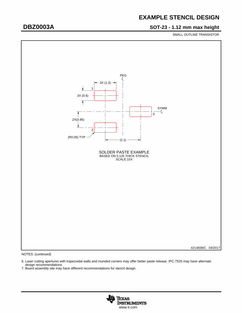
www.ti.com
EXAMPLE STENCIL DESIGN
(2.1)
2X(0.95)
3X (1.3)
3X (0.6)
(R0.05) TYP
SOT-23 - 1.12 mm max heightDBZ0003ASMALL OUTLINE TRANSISTOR
4214838/C 04/2017
NOTES: (continued) 6. Laser cutting apertures with trapezoidal walls and rounded corners may offer better paste release. IPC-7525 may have alternate design recommendations. 7. Board assembly site may have different recommendations for stencil design.
SOLDER PASTE EXAMPLEBASED ON 0.125 THICK STENCIL
SCALE:15X
SYMM
PKG
1
3
2
IMPORTANT NOTICE
Texas Instruments Incorporated (TI) reserves the right to make corrections, enhancements, improvements and other changes to itssemiconductor products and services per JESD46, latest issue, and to discontinue any product or service per JESD48, latest issue. Buyersshould obtain the latest relevant information before placing orders and should verify that such information is current and complete.TI’s published terms of sale for semiconductor products (http://www.ti.com/sc/docs/stdterms.htm) apply to the sale of packaged integratedcircuit products that TI has qualified and released to market. Additional terms may apply to the use or sale of other types of TI products andservices.Reproduction of significant portions of TI information in TI data sheets is permissible only if reproduction is without alteration and isaccompanied by all associated warranties, conditions, limitations, and notices. TI is not responsible or liable for such reproduceddocumentation. Information of third parties may be subject to additional restrictions. Resale of TI products or services with statementsdifferent from or beyond the parameters stated by TI for that product or service voids all express and any implied warranties for theassociated TI product or service and is an unfair and deceptive business practice. TI is not responsible or liable for any such statements.Buyers and others who are developing systems that incorporate TI products (collectively, “Designers”) understand and agree that Designersremain responsible for using their independent analysis, evaluation and judgment in designing their applications and that Designers havefull and exclusive responsibility to assure the safety of Designers' applications and compliance of their applications (and of all TI productsused in or for Designers’ applications) with all applicable regulations, laws and other applicable requirements. Designer represents that, withrespect to their applications, Designer has all the necessary expertise to create and implement safeguards that (1) anticipate dangerousconsequences of failures, (2) monitor failures and their consequences, and (3) lessen the likelihood of failures that might cause harm andtake appropriate actions. Designer agrees that prior to using or distributing any applications that include TI products, Designer willthoroughly test such applications and the functionality of such TI products as used in such applications.TI’s provision of technical, application or other design advice, quality characterization, reliability data or other services or information,including, but not limited to, reference designs and materials relating to evaluation modules, (collectively, “TI Resources”) are intended toassist designers who are developing applications that incorporate TI products; by downloading, accessing or using TI Resources in anyway, Designer (individually or, if Designer is acting on behalf of a company, Designer’s company) agrees to use any particular TI Resourcesolely for this purpose and subject to the terms of this Notice.TI’s provision of TI Resources does not expand or otherwise alter TI’s applicable published warranties or warranty disclaimers for TIproducts, and no additional obligations or liabilities arise from TI providing such TI Resources. TI reserves the right to make corrections,enhancements, improvements and other changes to its TI Resources. TI has not conducted any testing other than that specificallydescribed in the published documentation for a particular TI Resource.Designer is authorized to use, copy and modify any individual TI Resource only in connection with the development of applications thatinclude the TI product(s) identified in such TI Resource. NO OTHER LICENSE, EXPRESS OR IMPLIED, BY ESTOPPEL OR OTHERWISETO ANY OTHER TI INTELLECTUAL PROPERTY RIGHT, AND NO LICENSE TO ANY TECHNOLOGY OR INTELLECTUAL PROPERTYRIGHT OF TI OR ANY THIRD PARTY IS GRANTED HEREIN, including but not limited to any patent right, copyright, mask work right, orother intellectual property right relating to any combination, machine, or process in which TI products or services are used. Informationregarding or referencing third-party products or services does not constitute a license to use such products or services, or a warranty orendorsement thereof. Use of TI Resources may require a license from a third party under the patents or other intellectual property of thethird party, or a license from TI under the patents or other intellectual property of TI.TI RESOURCES ARE PROVIDED “AS IS” AND WITH ALL FAULTS. TI DISCLAIMS ALL OTHER WARRANTIES ORREPRESENTATIONS, EXPRESS OR IMPLIED, REGARDING RESOURCES OR USE THEREOF, INCLUDING BUT NOT LIMITED TOACCURACY OR COMPLETENESS, TITLE, ANY EPIDEMIC FAILURE WARRANTY AND ANY IMPLIED WARRANTIES OFMERCHANTABILITY, FITNESS FOR A PARTICULAR PURPOSE, AND NON-INFRINGEMENT OF ANY THIRD PARTY INTELLECTUALPROPERTY RIGHTS. TI SHALL NOT BE LIABLE FOR AND SHALL NOT DEFEND OR INDEMNIFY DESIGNER AGAINST ANY CLAIM,INCLUDING BUT NOT LIMITED TO ANY INFRINGEMENT CLAIM THAT RELATES TO OR IS BASED ON ANY COMBINATION OFPRODUCTS EVEN IF DESCRIBED IN TI RESOURCES OR OTHERWISE. IN NO EVENT SHALL TI BE LIABLE FOR ANY ACTUAL,DIRECT, SPECIAL, COLLATERAL, INDIRECT, PUNITIVE, INCIDENTAL, CONSEQUENTIAL OR EXEMPLARY DAMAGES INCONNECTION WITH OR ARISING OUT OF TI RESOURCES OR USE THEREOF, AND REGARDLESS OF WHETHER TI HAS BEENADVISED OF THE POSSIBILITY OF SUCH DAMAGES.Unless TI has explicitly designated an individual product as meeting the requirements of a particular industry standard (e.g., ISO/TS 16949and ISO 26262), TI is not responsible for any failure to meet such industry standard requirements.Where TI specifically promotes products as facilitating functional safety or as compliant with industry functional safety standards, suchproducts are intended to help enable customers to design and create their own applications that meet applicable functional safety standardsand requirements. Using products in an application does not by itself establish any safety features in the application. Designers mustensure compliance with safety-related requirements and standards applicable to their applications. Designer may not use any TI products inlife-critical medical equipment unless authorized officers of the parties have executed a special contract specifically governing such use.Life-critical medical equipment is medical equipment where failure of such equipment would cause serious bodily injury or death (e.g., lifesupport, pacemakers, defibrillators, heart pumps, neurostimulators, and implantables). Such equipment includes, without limitation, allmedical devices identified by the U.S. Food and Drug Administration as Class III devices and equivalent classifications outside the U.S.TI may expressly designate certain products as completing a particular qualification (e.g., Q100, Military Grade, or Enhanced Product).Designers agree that it has the necessary expertise to select the product with the appropriate qualification designation for their applicationsand that proper product selection is at Designers’ own risk. Designers are solely responsible for compliance with all legal and regulatoryrequirements in connection with such selection.Designer will fully indemnify TI and its representatives against any damages, costs, losses, and/or liabilities arising out of Designer’s non-compliance with the terms and provisions of this Notice.
Mailing Address: Texas Instruments, Post Office Box 655303, Dallas, Texas 75265Copyright © 2018, Texas Instruments Incorporated

![SITRANS F C MASSFLO - Siemens · SITRANS F C MASSFLO ... 50 50 50 50 50 50 50 50 Equivalent cable must have Lc/Rc ratio lower or equal to 100 [µh/Ω]. SITRANS F C MASSFLO ...](https://static.fdocument.org/doc/165x107/5add07b37f8b9aa5088c4cf1/sitrans-f-c-massflo-siemens-f-c-massflo-50-50-50-50-50-50-50-50-equivalent.jpg)