
Rapid Prototyping of Hybrid, Plastic-Quartz 3D-Chips for
20
10 Rapid Prototyping of Hybrid, Plastic-Quartz 3D-Chips for Battery-Operated Microplasmas Weagant S., Li L. and Karanassios V. University of Waterloo, Department of Chemistry Canada 1. Introduction The word prototype is derived from the Greek ǑǒωǕǝǕǖǑǐν (pronounced prototypon) which is a combination of two words: ǑǒώǕǐǓ (protos meaning first) and ǕǞǑoǓ (typos meaning type or instance). Despite of exactness in etymology, there is multiplicity in semantics. For example, Webster’s lists four definitions for prototype with each definition having a slightly-different context-dependent meaning. Figuratively, a prototype (i.e., the first instance or version of something) can be defined as a functioning model or a physical object that can be used to test concepts or ideas. Although this broad definition applies to many branches of science and engineering, it has different meaning in biosciences and health-related disciplines. Furthermore, the term rapid prototyping is usually loosely associated with a variety of meanings depending on the context it is applied to. In software for instance, the term is typically used to imply the process of quickly coding (usually incomplete) versions of software that are often used to test or demonstrate (mostly) user interface design concepts (Karanassios & Horlick, 1987). In electronics, it is frequently used as a synonym for making a circuit board (sometimes using speedy wire-wrap methods) to verify an electronic design or to provide a practical means for debugging it (Karanassios & Horlick, 1988). Literally, the definition of rapid prototyping is the ability to generate relatively quickly a corresponding 3d physical object or an actual device (i.e., a fully functioning mechanical part or its scaled down version) from its 3d representation from a virtual computer model. The word “rapid” is relative as compared to the speed of conventional methods of generating the same 3d physical object or prototype. Inherent to the definition is the implication that one or a few prototypes need to be made. Implied by the definition is that this quick concept-to-prototype approach is relatively low-cost (as compared to conventional methods). Conceptually, there are two basic methods of making prototypes of 3d-objects. The first method involves removal of material using a subtractive method. This is referred to as a top-down approach. In this (often material-wasteful) approach, material gets removed from a solid block in order to make a physical, 3d-object. Removed material typically gets discarded. Traditionally, lathes, milling machines and Computer Numerical Controlled (CNC) machines have been used to make solid 3d-objects that are in the mm range or larger. One way of making objects that are mm-size or smaller (e.g., sub-mm or micro-meter) is by using bulk micromachining techniques. Bulk micromachining (or simply micromachining) www.intechopen.com
Transcript of Rapid Prototyping of Hybrid, Plastic-Quartz 3D-Chips for

10
Rapid Prototyping of Hybrid, Plastic-Quartz 3D-Chips for Battery-Operated Microplasmas
Weagant S., Li L. and Karanassios V. University of Waterloo, Department of Chemistry
Canada
1. Introduction
The word prototype is derived from the Greek ┨┩ω┬┴┬┭┨┧ν (pronounced prototypon) which is a combination of two words: ┨┩ώ┬┧┪ (protos meaning first) and ┬┵┨o┪ (typos meaning type or instance). Despite of exactness in etymology, there is multiplicity in semantics. For example, Webster’s lists four definitions for prototype with each definition having a slightly-different context-dependent meaning. Figuratively, a prototype (i.e., the first instance or version of something) can be defined as a functioning model or a physical object that can be used to test concepts or ideas. Although this broad definition applies to many branches of science and engineering, it has different meaning in biosciences and health-related disciplines. Furthermore, the term rapid prototyping is usually loosely associated with a variety of meanings depending on the context it is applied to. In software for instance, the term is typically used to imply the process of quickly coding (usually incomplete) versions of software that are often used to test or demonstrate (mostly) user interface design concepts (Karanassios & Horlick, 1987). In electronics, it is frequently used as a synonym for making a circuit board (sometimes using speedy wire-wrap methods) to verify an electronic design or to provide a practical means for debugging it (Karanassios & Horlick, 1988). Literally, the definition of rapid prototyping is the ability to generate relatively quickly a corresponding 3d physical object or an actual device (i.e., a fully functioning mechanical part or its scaled down version) from its 3d representation from a virtual computer model. The word “rapid” is relative as compared to the speed of conventional methods of generating the same 3d physical object or prototype. Inherent to the definition is the implication that one or a few prototypes need to be made. Implied by the definition is that this quick concept-to-prototype approach is relatively low-cost (as compared to conventional methods). Conceptually, there are two basic methods of making prototypes of 3d-objects. The first method involves removal of material using a subtractive method. This is referred to as a top-down approach. In this (often material-wasteful) approach, material gets removed from a solid block in order to make a physical, 3d-object. Removed material typically gets discarded. Traditionally, lathes, milling machines and Computer Numerical Controlled (CNC) machines have been used to make solid 3d-objects that are in the mm range or larger. One way of making objects that are mm-size or smaller (e.g., sub-mm or micro-meter) is by using bulk micromachining techniques. Bulk micromachining (or simply micromachining)
www.intechopen.com
Rapid Prototyping Technology – Principles and Functional Requirements
210
also follows a top-down approach. Traditionally, a mask and photolithography are used to transfer a design onto a chip, and “dry” or “wet” etching are used to fabricate a design that was photolithographically transferred onto-a-chip. Because in micromachining using fabrication technology borrowed from the semiconductor industry the depth of structures is typically in the μm-range, microfabrication techniques yield structures or objects that are “flatter” that is, they are primarily 2d (with some height or perspective added to them). Thus, for the most part micromachined devices are not considered as “true” 3d-objects. The second method of prototyping 3d-objects involves addition of material one-layer-at-a-time that is by using a bottom-up approach. Among other techniques, 3d-printing approaches are often used and inexpensive 3d printers (including desktop models) are currently commercially available. To many in this field and in a strict sense, rapid prototyping is synonymous with a variety of additive methods. In this chapter, this definition will be adhered to. There are many such methods. Examples include stereo-lithography (SLA), selective laser sintering (SLS), fused deposition modeling (FMD), direct metal laser sintering (DMLS), PolyJet and other 3d printers. For the work described here, 3d Micro Plasma Devices (MPDs) on plastic substrates were prototyped using a subtractive and an additive method to prototype exactly the same device. This was done to enable direct comparisons. Devices so prototyped will be contrasted with flatter (primarily 2d) microplasma devices prototyped using a mask, photolithography, microfabrication technology and wet chemical etching of microfluidic channels on glass or crystalline Si chips (Karanassios & Mew, 1997; Karanassion & Sharples, 1997a; Karanassios & Sharples, 1977b; Swart et al., 1997). The plastic, glass or crystalline Si chips became hybrid when they were fitted with a quartz plate. The plate was added because quartz is optically transparent to ultra-violet (UV), as required for measurements in this spectral region. These microplasma devices on hybrid chips (with area roughly that of a small postage stamp) were used for development and characterization of microplasmas primarily for elemental analysis applications (Karanassios, 2004; Karanassios et al., 2007; Weagant & Karanassios, 2009, Weagant et al., 2011; Karanassios, 2011). Elemental analysis is as a sub-set of the discipline called chemical analysis or analytical chemistry.
2. Justification
In this section, questions such as “why use microplasmas?” and “how does one fabricate microplasma devices?” will be used to address analytical capability and utility, and to rationalize the need for and applicability of rapid prototyping methods for microplasma device fabrication.
2.1 Why microplasmas?
Microplasmas have been arbitrarily defined as electrical discharges with at least one dimension in the range spanning between micro-meters to about a mm (Karanassios, 2004). Although microplasmas are a relatively new research area, they are beginning to attract significant interest in areas as diverse as science, engineering, medicine and technology (Tachibana, 2006; Becker et al., 2006; Iza et al, 2008; Foest et al., 16; Becker et al., 2010). To give a limited number of examples, in physics they are used as light sources for spectroscopy (Tachibana, 2006); in materials science for nanomaterials synthesis (Zou et al.,
www.intechopen.com
Rapid Prototyping of Hybrid, Plastic-Quartz 3D-Chips for Battery-Operated Microplasmas
211
2009; Sankaran et al., 2005; Chiang et al., 2007; Sankaran, 2011; Mariotti & Sankaran, 2011; Mariotti & Sankaran, 2010; Chian & Sankaran, 2010); in medicine for sterilization (Uhm & Hong, 2011) and for plasma medicine (Kim et al., 2010; Heinlin et al., 2010; Fridman et al., 2008; Kong et al., 2009); in technology for lighting applications (Readle et al., 2007; Boertner et al., 2010) and for plasma television (Boeuf, 2003; Petrovic et al., 2008; Kim et al., 2009; Mun et al., 2009; Kim et al., 2010; Lee et al., 2011). In chemistry, among other applications they are used for chemical analysis of samples (e.g., elemental analysis of water samples). Environmental monitoring of liquid samples (e.g., water) is the intended application of the microplasmas we are developing using prototyping methods.
2.2 Why use microplasmas for chemical analysis?
For chemical analysis, the drive behind development of microplasmas operating at atmospheric pressure stems from a potential for development of plasma sources that are low-cost, small-size, light-weight and that have reduced gas-consumption and low power-requirements (thus enabling battery-operation) and no vacuum requirements. Furthermore, because they are typically non-thermal discharges, they do not require water-cooling or other thermal management, thus further reducing weight, instrumentation complexity, electrical power requirements and cost. These desirable attributes facilitate development of solar-powered, battery-operated, mobile analytical instruments with advanced wireless capabilities for possible use in the field (i.e., on-site) (Karanassios, 2011). The needs for mobile chemical analysis instruments that can be used for on-site analytical measurements can be justified by considering, for example, environmental monitoring, quality control of produce and food industry, or homeland security where applications exist in abundance. This potential and applicability of microplasmas has been recognized by many. For instance, there are several research groups world-wide working on microplasmas for chemical analysis applications. Thus far, microplasmas have been described in books (Becker et al., 2004; Hutchison, 2005; Lieberman, 2005; Fridman, 2008; Hippler at al., 2008; Fridman, 2011; Inan & Gokowski, 2011), in review articles (Karanassios, 2004; Broekaert & Siemens, 2004; Broekaert & Jakubowski, 2007; Gianchandani et al., 2009) and in papers describing their analytical applications (Karanassios et al., 2007; Weagant & Karanassios, 2009; Weagant et al., 2010; Weagant et al., 2011; Vautz et al., 2008; Olenici-Craciunescu, 2009; Hoskinson et al., 2011; Marcus et al., 2011), their characteristics and their other uses (Janasek et al., 2006; Frimat et al., 2009; Olenici-Craciunescu, 2011; Xu & Hopwood, 2007; Zhu et al., 2008; Chen & Eden, 2008; Wright & Chianchandani, 2009; Walsh et al., 2010; McKay et al., 2010; Walsh et al., 2010; Liu et al., 2010). From the cited literature it can be concluded that although microplasma research has been (mostly) application driven, “microplasmas represent a new realm in plasma physics that still is
not fully understood” (Iza, 2008). And that microplasmas are receiving significant current attention due to their potential economic and technological impact in many disciplines. Then, how does one develop prototype microplasma devices for instance, for possible use in on-site chemical analysis applications using portable, battery-operated instruments?
3. Prototyping microplasma devices
In this section the rationale, justification and different methods that were used for prototyping microplasma devices will be described in some detail.
www.intechopen.com
Rapid Prototyping Technology – Principles and Functional Requirements
212
3.1 Prototyping microplasma devices in microfluidic channels using microfabrication
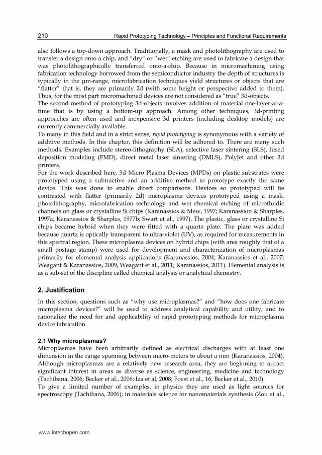
Several planar geometry microplasma devices were microfabricated using a mask, photolithography and wet chemical etching (Karanassios & Mew, 1997; Karanassios & Sharples, 1997a; Karanassios & Sharples, 1997b; Swart et al., 1997) of microfluidic channels. Initially, microplasma devices were fabricated across microfluidic channels that were about 30 μm deep and were etched in crystalline Silicon (c-Si). An example of an etched microfluidic channel is shown in Fig. 1. Two holes were drilled at the end of the microchannel (not shown in Fig. 1 for brevity). One hole served as the carrier-gas and sample introduction inlet and the other as the outlet. The etched microchannel was covered by a glass or a quartz plate. Electrodes were sputter deposited on one of the surfaces of the plate and the plate was positioned so that the electrodes were facing the microchannel. The sputter electrodes also served as contact pads. The chip and the plate were aligned and were bonded (Karanassios et al., 2007) to provide hermetic seal.
Fig. 1. Color on-line. Photograph (taken under 60 fold magnification) of a wet-etched micro-fluidic channel on crystalline Si that was used for fabrication of microplasma devices. See text for discussion.
To reduce the costs of prototyping a new microplasma device any time one of the electrodes was damaged and to enable deeper etches crystalline silicon wafers were replaced by amorphous glass wafers (or substrates). Glass was selected due to its low cost and ease of wet chemical etching of deep micro-channels (e.g. >100 μm). On the glass chip, a microfluidic channel (in geometry somewhat resembling a rotated letter “Z”) was patterned and it was etched using either HF or buffered HF (Karanassios et. al., 2007). Several microchannel geometries were tested with microchannel depths ranging from 150 μm to 500 μm. Holes were drilled at both ends of the microchannel and tubes were affixed to the holes. One tube served as the sample introduction and carrier gas inlet and the other as the outlet. On the quartz plate, 60 nm-thick to 120 nm-thick electrodes were sputter deposited on one of its surfaces and this wafer was placed on top of the etched wafer so that the electrodes were facing the microchannel. An example is shown in Fig. 2. The chips were bonded to provide a hermetic seal (Karanassios et al., 2007). A high voltage dc (HVdc) was applied between the sputtered electrodes to initiate and sustain the microplasma. Due to the application of HVdc, the electrodes were often stressed to the point of being damaged. Invariably, damaged electrodes necessitated replacement of the microplasma device (thus having to prototype a new one). In addition to cost, only shallow microchannels could be etched because wet chemical etching of deep channels (e.g., >100 μm) has been found to affect the integrity of the side-walls and of the bottom of the etched channels (Karanassios & Mew, 1997; Karanassios & Sharples, 1997a; Karanassios & Sharples,
www.intechopen.com

Rapid Prototyping of Hybrid, Plastic-Quartz 3D-Chips for Battery-Operated Microplasmas
213
1997b; Swart et al., 1997). Poor quality and shallow depth of the microchannels affected both sample introduction and stability of microplasma background emission. To increase microplasma-microsample interaction a device with a deeper microchannel was needed. For this, the depth of the microplasma channel had to be increased and the width of the electrodes had to be enlarged. For prototyping purposes, 3 wafers were used: two were made out of glass and one out of quartz.
Fig. 2. Color on-line. Two-chip, planar-geometry microplasma device prototyped as briefly described above (see text for discussion).
Specifically, for the middle wafer, a channel was etched right through and shallow channels and pits were etched on the top and bottom wafers. Electrodes were made from a variety of commercially available metallic materials (e.g., thin ribbons of Ni, Mo, Re etc.). The thin ribbons were partially wrapped around the narrow opening of the etched-though channel of the middle wafer (Fig. 3). The ends of the ribbon-electrodes were connected to high voltage power supply. On the top glass wafer holes were drilled through the wafer, and tubes that served as inlet and outlet were affixed to them. The bottom wafer was made out of quartz. This made this 3-wafer microplasma device more “3d-like”. An example of this 3d-like, three-wafer (or three-chip) microplasma device is shown in Fig. 3. The internal volume of the microplasma channel of the type shown in Fig. 3 was between 200 nL and 750 nL, thus giving rise to the term “nano-volume” plasmas or “nano-palasmas” for short. These were so named by analogy to nano-electrospray and to nano flow injection. As before, the chips were bonded to provide a hermetic seal (Karanassios et al., 2007). To reduce or eliminate electrode stress from the high voltage dc (HVdc) applied to the electrodes, the HVdc power supply was replaced by a high voltage ac (HVac) power supply. More specifically, a low voltage dc power supply (or either an 8V or a 12V or an 18 V rechargeable battery) was used to power a dc-to HVac power supply. The high voltage ac was applied between the ribbon electrodes. Upon application of the HVac, the plasma was ignited and an atmospheric pressure plasma discharge was formed inside the channel between the two electrodes (Fig. 3). Thus, a planar-geometry, self-igniting, atmospheric pressure microplasma device was prototyped.
www.intechopen.com
Rapid Prototyping Technology – Principles and Functional Requirements
214
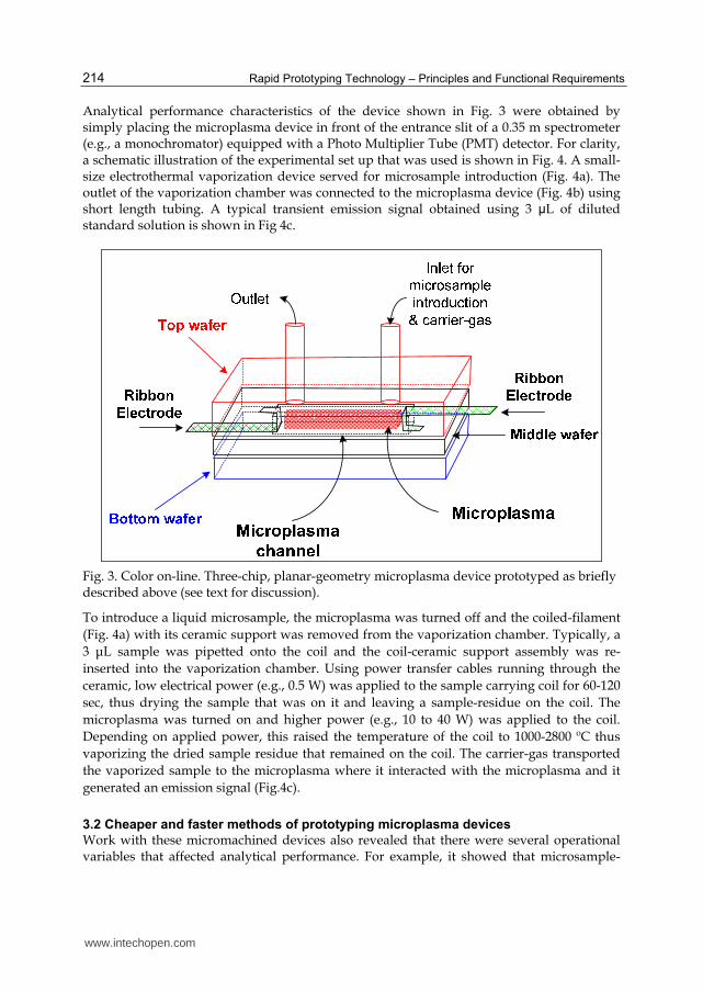
Analytical performance characteristics of the device shown in Fig. 3 were obtained by simply placing the microplasma device in front of the entrance slit of a 0.35 m spectrometer (e.g., a monochromator) equipped with a Photo Multiplier Tube (PMT) detector. For clarity, a schematic illustration of the experimental set up that was used is shown in Fig. 4. A small-size electrothermal vaporization device served for microsample introduction (Fig. 4a). The outlet of the vaporization chamber was connected to the microplasma device (Fig. 4b) using short length tubing. A typical transient emission signal obtained using 3 μL of diluted standard solution is shown in Fig 4c.
Fig. 3. Color on-line. Three-chip, planar-geometry microplasma device prototyped as briefly described above (see text for discussion).
To introduce a liquid microsample, the microplasma was turned off and the coiled-filament (Fig. 4a) with its ceramic support was removed from the vaporization chamber. Typically, a 3 μL sample was pipetted onto the coil and the coil-ceramic support assembly was re-inserted into the vaporization chamber. Using power transfer cables running through the ceramic, low electrical power (e.g., 0.5 W) was applied to the sample carrying coil for 60-120 sec, thus drying the sample that was on it and leaving a sample-residue on the coil. The microplasma was turned on and higher power (e.g., 10 to 40 W) was applied to the coil. Depending on applied power, this raised the temperature of the coil to 1000-2800 ºC thus vaporizing the dried sample residue that remained on the coil. The carrier-gas transported the vaporized sample to the microplasma where it interacted with the microplasma and it generated an emission signal (Fig.4c).
3.2 Cheaper and faster methods of prototyping microplasma devices
Work with these micromachined devices also revealed that there were several operational variables that affected analytical performance. For example, it showed that microsample-
www.intechopen.com

Rapid Prototyping of Hybrid, Plastic-Quartz 3D-Chips for Battery-Operated Microplasmas
215
microplasma interactions are important as are: inter-electrode distance; electrode size, composition and geometrical configuration; inlet and outlet geometries (due to potential for sample loss primarily on the sharp corners of channels) and microplasma dimensions as defined by channel length, width and depth, and electrode size. As expected, the effect of these parameters must be experimentally verified by prototyping new devices. But fabrication cost alone made microfabrication of large numbers of prototypes prohibitive. In addition to cost, there was significant time-delay between design, mask-making, photolithography, etching, aligning and hermetically sealing the hybrid chips. Thus,
Time (s)
0 1 2 3 4 5
Inte
ns
ity
(A
. U
.)
0.0
0.1
0.2
0.3
0.4
0.5
0.6
0.7
PM
T
Dete
cto
r
Exit
sli
t
En
tra
nce s
lit
Ou
tlet
Ar/
H2
Fig. 4. Color on-line, illustrations not to scale. a) Schematic of microsample introduction system. b) Schematic of the spectrometer used for single-channel (or single wavelength) acquisition of optical emission analyte-signals using a PMT-based spectrometer. The microplasma was formed between electrodes E1 and E2 following application of high voltage. Often, the battery (shown in part b of this figure) was charged by a solar panel. And c), typical emission signal from 1.5 ng Ca.
www.intechopen.com
Rapid Prototyping Technology – Principles and Functional Requirements
216
an alternative fabrication method was sought utilized. Therefore, finding a cheaper and faster way of prototyping microplasma devices became a key goal. In addition to the effect of operational parameters on analytical performance characteristics, the work described thus far demonstrated that microfabricated devices can be operated using low electrical power levels (<10 W), so much so that they could be powered from a rechargeable battery (Weagant et al., 2011). It also revealed that microplasmas are non-thermal discharges, thus cooling or other thermal management is not required. These facilitated portability by reducing weight and complexity of microplasma instrumentation. Importantly, their low operating temperature opened up the possibility for using polymeric (e.g., plastic) substrates. In turn, this opened up another possibility, namely that of prototyping microplasma devices using inexpensive machining of plastic substrates.
3.3 Prototyping microplasma devices via machining of plastic substrates
Poly-tetra-fluoro-ethylene (PTFE, marketed as the Dubon Corp.-made Teflon®) was chosen as the substrate. This polymeric (i.e., plastic) material was selected because it is easy to machine, due to its desirable mechanical and electrical properties and its tolerance due to its desirable mechanical and electrical properties and its tolerance to temperatures up to about 260 ºC. But since conventional machining could not be used to fabricate micro-meter size fluidic channels as required for fabrication of microplasma devices, channel dimensions had to be enlarged. But then, would plasma discharges formed inside enlarged channels fit the definition of microplasma (as stated earlier)? To address this question, several designs were tested. For the final design, a channel was machined by removing a 2.0 mm wide, 16.3 mm long and 8.7 mm deep ellipsoid from a PTFE chip (38.1 mm long, 12.7 mm wide and 12.7 mm tall); by drilling a 3.2 mm diameter round hole for carrier-gas and sample introduction inlet and a 7.1 mm diameter round hole for the outlet. These holes were drilled through the opposing short-size vertical 12.7 mm walls. Two needle electrodes were inserted through the opposing, long-side vertical walls into the microplasma channel (Fig. 5). Although many inter-electrode distances and electrode diameters were tested for ease of plasma ignition and stability of optical emission of microplasma background, an inter-electrode distance of 12 mm and a 1.2 mm diameter needle-electrode (for the electrode closer to the outlet) and 1.6 mm diameter needle-electrode (for the electrode closer to the outlet) provided the most stable microplasma operation and it was used throughout. In addition, a counter-sank rectangle was machined out of the top face of the PTFE chip (Fig. 5), so that a 2.0 mm thick quartz plate would fit tightly in it, thus also providing a tight seal. Overall, the machining approach simplified sealing vis-à-vis the micromachined devices, thus making prototyping cheaper and relatively faster. An Ar-H2 (Weagant et al., 2011) gas mixture served as the carrier-gas and as the microplasma gas. When a carrier-gas with a typical flow-rate around 220 mL/min was introduced into the microplasma channel through the outlet and HVac was applied between the electrodes (Figs. 4 and 5), a self-igniting microplasma discharge was formed between the electrodes inside the microplasma channel. A photograph of the plasma and of the hybrid chip that was prototyped as described above is shown in Fig. 5. From the insert (Fig. 5), it can be concluded that the plasma formed between the electrodes is indeed microplasma. Optical emission was monitored using a fiber optic spectrometer with a Charge Coupled Device (CCD) detector. An example is shown in Fig. 6. Unlike the single-channel, PMT-based spectrometer (Fig. 4), using the multi-channel CCD-based, fiber-optic spectrometer the wavelength range between 200 nm and 850 nm could be monitored simultaneously.
www.intechopen.com

Rapid Prototyping of Hybrid, Plastic-Quartz 3D-Chips for Battery-Operated Microplasmas
217
MicroplasmaTeflon®
Electrode
Electrode
Insert
Quartz plate
Inle
t
Inlet for microsample introduction
and carrier gas
Quartz plate
Needle
Electrode
Needle
Electrode
Microplasma
Outlet
Teflon®
Microplasma
channel
Fiber optic cable to
CCD spectrometer
Fig. 5. (Color on-line.) Schematic illustration (not to scale) of a microplasma device and shown in insert is a labeled photograph of the microplasma device. A Canadian one-cent coin has been included for size. As shown in the insert, the microplasma fits comfortably inside the letter A of the coin, thus confirming that the plasma discharge formed between the two electrodes is micro-size, thus following the microplasma definition.The fiber-optic cable was positioned on top of the quartz plate.
Pa
rt of fib
er o
ptic
cab
le
Fig. 6. (Color on-line, schematic is not to scale.) Fiber-optic, CCD-based spectrometer.
Although machining of plastic chips enabled inexpensive prototyping of microplasma devices, there was still some time-delay between design and prototyping. These were
www.intechopen.com

Rapid Prototyping Technology – Principles and Functional Requirements
218
primarily due to scheduling and logistics of the local machine shop. Thus the original goal of fabricating microplasma devices cheaper and faster was only partially fulfilled. Can the concept-design-prototype time-cycle be shortened even further while still maintaining a low-cost advantage of using plastics? To address this question, an additive method was used.
3.4 Rapid prototyping of microplasma devices via 3d-printing of plastics
In this additive method of rapid prototyping, a 3d-printer and ABS (acrylonitrile butadiene styrene) plastic were used. Briefly, in additive 3d printing method, the printer receives 3d CAD (Computer Aided Design) data. There are many ways in which a 3d-printer can use these data. For example, it can lay down successive thin layers (e.g., a few 100’s of μm or less) of a variety of materials. Examples include slurries, ceramic powders or even metals. Conceptually, these layers correspond to cross-sections of a virtual 3d model typically displayed a computer screen. To simplify description, it is assumed that the printer lays down thin layers of UV-curable plastic. These layers are joined or fused together using UV light to create the desired final shape. Low-cost, relative high-speed of making fully-functioning physical 3d-objects or prototypes and reduced waste are key advantages of 3d-printing. And because software drives a 3d-printer, each 3d-object can have different dimensions without the requirement for expensive retooling. For instance, microplasma devices with different dimensions and geometries could be printed inexpensively in about 30 min or less. Thus, the original goal of cheaper and faster fabrication was fulfilled. An example of a microplasma device rapidly prototyped via 3d-printing is shown in Fig. 7a. The surface quality (e.g., texture, roughness) of the 3d-printed device (Fig. 7b) was compared with that of the machined device (Fig. 7c). As can be concluded from Fig. 7b and 6c, surface quality is different. Would surface quality affect analytical performance?
4. Experimental, results and discussion
The machined and the rapidly prototyped (via 3d-printing) microplasma devices were tested by introducing into them 3 μL samples using the small-size electrothermal vaporization micro-sample introduction system briefly described earlier. Transient, optical emission signals were recorded using a portable, fiber-optic spectrometer equipped with CCD detector (Weagant & Karanassios, 2009). An example signal is shown in Fig. 8. Briefly, analyte emission signals from 3 μL samples lasted for less than 1 second and the microplasma was turned on for only about 5 sec. In some cases, a short microplasma stabilization time was added. The relatively brief period the microplasma was turned on conserved electrical energy (thus increasing battery life). No doubt, it also reduced over-heating that may have resulted from prolonged microplasma operation, thus further enabling use of plastic substrates. To facilitate comparisons the same samples were run using the machined and the 3d-printed MPDs. Statistically, the signals obtained from the machined microplasma device were indistinguishable from those obtained using the printed one. Clearly, surface quality did not affect analytical performance characteristics, at least for the elements tested thus far. The detection limit (defined as the lowest amount or concentration that can be detected with a stated statistical confidence) obtained with both of these devices were in the pico-gram (pg) range (using the 3┫ criterion). These are impressive considering the simplicity of the prototyped devices and that emission data were obtained from micro-liter volume samples.
www.intechopen.com

Rapid Prototyping of Hybrid, Plastic-Quartz 3D-Chips for Battery-Operated Microplasmas
219
In some respects, they also highlight the significance of microplasma-microsample introduction (likely facilitated by enlarging the microplasma channel) and by making the diameter of the outlet of the microsample introduction system more compatible with the diameter of the microplasma.
Fig. 7. (Color on-line.) Photographs of: a) a 3d printed microplasma device with a coin included for size; b) the front side of the 3d-printed device (taken under 60x magnification); and c) the front side of the device machined out of PTFE (taken under 60x magnification).
www.intechopen.com
Rapid Prototyping Technology – Principles and Functional Requirements
220
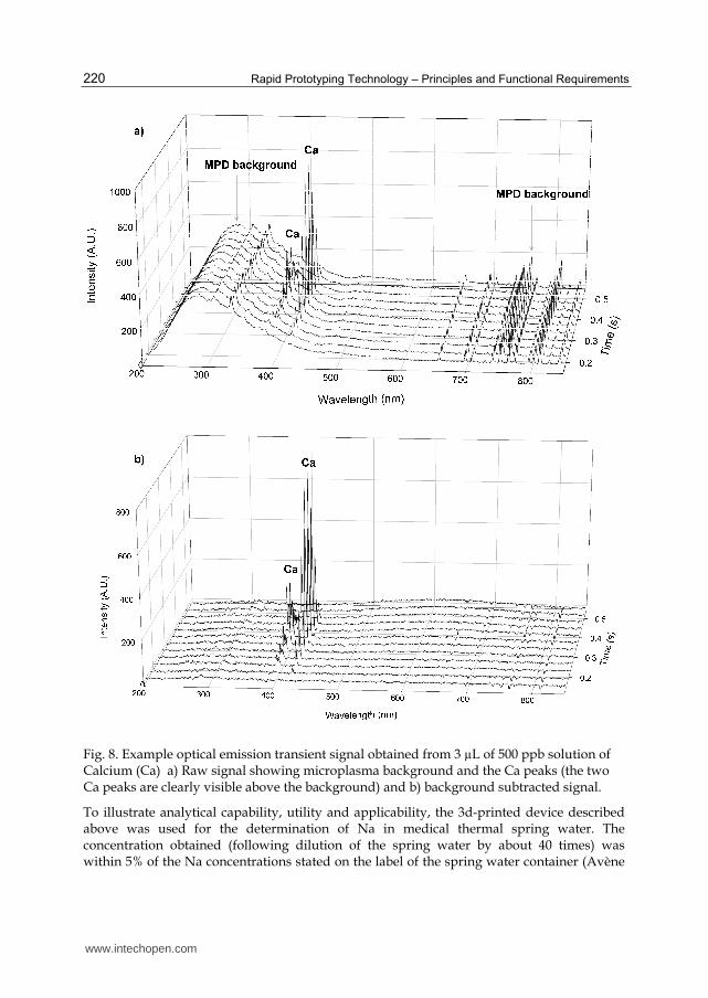
Fig. 8. Example optical emission transient signal obtained from 3 µL of 500 ppb solution of Calcium (Ca) a) Raw signal showing microplasma background and the Ca peaks (the two Ca peaks are clearly visible above the background) and b) background subtracted signal.
To illustrate analytical capability, utility and applicability, the 3d-printed device described above was used for the determination of Na in medical thermal spring water. The concentration obtained (following dilution of the spring water by about 40 times) was within 5% of the Na concentrations stated on the label of the spring water container (Avène
www.intechopen.com

Rapid Prototyping of Hybrid, Plastic-Quartz 3D-Chips for Battery-Operated Microplasmas
221
USA, Pierre Fabre Dermo Cosmétique USA, 9 Campus Drive, Suite 2, Parsippany, NJ 07054). The determination of Na concentration demonstrates that prototyped microplasma devices cannot only be used to study the effect experimental and design variables on analytical performance characteristics, but that they can also be used obtain useful analytically results.
5. Conclusions and outlook
Using semiconductor fabrication technology it was demonstrated that microplasma devices that are useful for elemental (i.e., chemical) analysis applications can be prototyped. Using these early prototypes, it was shown that analytical performance characteristics depended on a relatively large number of experimental and device-dependent parameters (e.g., device geometry and dimensions, electrode geometry and size). Study of the effect these parameters have on analytical performance characteristics necessitated fabrication of new prototype devices. Two key limitations to prototyping large numbers of microplasma devices were identified. One originated from costs involved with fabrication of a large number of one-of-a-kind research prototypes as opposed to fabricating relatively inexpensive but mass produced chips. The other arose from time-delays. For example, there was significant time-delay between mask-making, photolithography, etching, aligning and hermetically sealing hybrid microplasma device chips. These limitations hindered further progress in microplasma research. To expedite research, finding a cheaper and faster way of prototyping microplasma devices became a key research goal. Toward this goal, microplasma devices were initially prototyped using a subtractive method by simply machining PTFE substrates. This method reduced prototyping costs and substantially shortened time-delays. To reduce time-delays even further, an additive method of rapid prototyping (via 3d printing) was used. This method reduced concept-to-prototype time-delays while maintaining low cost, thus fulfilling the goal of cheaper and faster prototyping. Although analytical performance characteristics of microplasma devices that were prototyped using both a subtractive and an additive method were (statistically) the same, rapid prototyping via 3d printing provided the overall fastest turn-around time while maintaining low-cost. Using 3d-printing, microplasma devices with different geometries and dimensions could be inexpensively and rapidly prototyped, thus the effect experimental variables have on analytical performance characteristics of microplasmas could be delineated more expeditiously and at (relatively) lower cost. Thus far, rapid prototyping of 3d-objects one-layer-at-a-time has demonstrated that remarkable objects can be made. A limited set of examples includes medical implants, airplane parts, architectural designs and now microplasma devices. Looking forward, there is a school of thought suggesting that rapid prototyping via 3d-printing of digital designs will even transform conventional manufacturing (by analogy to desk-top 3d-printing) in the form of desk-top manufacturing. Conceivably and in addition to microplasma devices, other components of chemical analysis instruments (and perhaps even some small-size instruments) may be printed, thus reducing the overall cost of ownership of chemical analysis instrumentation. Undoubtedly, this will lead to wider use, applicability and utility of such instruments and will increase their societal and economic impact. In general, there is every indication that in the future rapid prototyping will be able to produce 3d objects that are not only cheaper and faster but may be even be of the same quality if not better than conventional than conventional prototyping methods.
www.intechopen.com

Rapid Prototyping Technology – Principles and Functional Requirements
222
6. Summary
Prototypes of battery-operated, atmospheric-pressure microplasma devices that were developed around microfluidic channels and were fabricated using technology borrowed from the semiconductor industry (e.g., photolithography and etching) demonstrated that analytical performance characteristics of these devices depends, on a relatively large number of experimental and device-dependent parameters (e.g., device geometry and dimensions, electrode geometry and size). Delineation of the effects these parameters have on analytical performance characteristics necessitated fabrication of new prototypes. But using semiconductor fabrication technology proved to be costly. Furthermore, it took a significant amount of time to go from concept-to-prototype due to the time required for mask-making, photolithography, etching, aligning and sealing. To facilitate microplasma research, a cheaper and faster way of prototyping microplasma devices was thought to be desirable. Toward this goal, microplasma devices were prototyped using a subtractive method by simply machining PTFE substrates. This method reduced costs and shortened time-delays. An additive method of prototyping was also used, it involved 3d-printing and it reduced time-delays even further. This method minimized concept-to-prototype time-delays while maintaining low cost, thus fulfilling the cheaper and faster prototyping goal. In this chapter, these prototyping methods were briefly discussed, compared and contrasted. Emission signals obtained using microsamples introduced into these prototype microplasma devices were used for comparison purposes. Statistically and for the elements tested, signals obtained using the machined microplasma devices were indistinguishable from those obtained using 3d-printed devices. Detection limits were impressive and were in the pg range (from micro-liter samples).
7. Acknowledgments
Financial assistance from the Natural Sciences and Engineering Research Council (NSERC) of Canada is gratefully acknowledged.
8. References
Becker, K. H., Kogelschatz, U., Schoenach, K. H. & Baker, R. J. (Eds.) (2004). Non-equilibrium air plasmas at atmospheric pressure, Taylor & Francis, ISBN-10: 0750309628
Becker, K. H., Schoenbach, K. H. & Eden, J. G. (2006). Microplasmas and applications, Journal of Physics D: Applied Physics, Vol. 39, pp. R55-R70, ISSN 1361-6463
Becker, K. H., Kersten, H., Hopwood, J., & Lopez, J. L. (2010). Microplasmas: scientific challenges & technological opportunities, European Physical Journal D., Vol. 60, pp. 437-439, ISSN 1434-6060
Boettner, H., Waskoenig, J., O'Connell, D., Kim, T. L., Tchertchian, P. A., Winter, J. & Schulz-von der Gathen, V. (2010). Excitation dynamics of micro-structured atmospheric pressure plasma arrays, Journal of Physics D: Applied Physics, Vol.43, pp. 124010, ISSN 1361-6463
Boeuf, J. P. (2003). Plasma display panels: physics, recent developments and key issues, , Journal of Physics D: Applied Physics, Vol.36, pp. R53, ISSN 1361-6463
www.intechopen.com

Rapid Prototyping of Hybrid, Plastic-Quartz 3D-Chips for Battery-Operated Microplasmas
223
Broekaert, J.A.C. & Siemens, V. (2004). Some trends in the development of microplasmas for spectrochemical analysis, Analytical and Bioanalytical Chemistry, Vol.380, pp. 185-189, ISSN 1618-2650
Broekaert, J. A. C. & Jakubowski, N. (2007). New plasma discharges for atomic spectroscopy, Analytical and Bioanalytical Chemistry, Vol. 388, pp. 1561-1563, ISSN 1618-2650
Chen, K.-F., Eden, J. G. (2008). The plasma transistor: A micro-cavity plasma device coupled with a low voltage, controllable electron emitter, Applied Physics Letters, Vol.93, pp. 161501, ISSN 0003-6951
Chiang, W.-H. & Sankaran, R. M. (2007), Microplasma synthesis of metal nano-particles for gas-phase studies of catalyzed carbon nano-tube growth, Applied Physics Letters, Vol.91, pp. 121503, ISSN 0003-6951
Chiang, W-H. & Sankaran, R. M. (2010). Continuous-flow, atmospheric-pressure microplasmas: A versatile source for metal nano-particle synthesis in the gas or liquid phase, Plasma Sources Science and Technology, Vol.19, pp. 034011, ISSN 1361-6595
Foest, R., Schmidt, M. & K. Backer, K. (2008). Microplasmas, an emerging field of low-temperature science and technology, International Journal of Mass Spectrometry, Vol.248, pp. 87-102, ISSN: 1387-3806
Fridman, Gutsol, A., Shekhter, A. B., Vasilets, V. N. & Fridman, A. (2008). Applied plasma medicine, Plasma Processes and Polymers, Vol.5, pp. 503-533, ISSN 1612-8869
Fridman, A. (2008). Plasma chemistry, Cambridge University Press, ISBN-13: 978-0521847353 Fridman, A. (2011), 2nd edition. Plasma physics and engineering, CRC Press, ISBN-13: 978-
1560328483 Frimat, J-P., Menne, H., Mitchels, A, Kittel, S., Kettler, R., Borgman, S., Franzke, J. & West,
W. (2009). Plasma stencilling method for cell patterning, Analytical and Bioanalytical Chemistry, Vol.395, pp. 601-609, ISSN 1618-2650
Gianchandani, Y. B., Wright, S., Eun, C., Wilson, C. & Mitra, B. (2009). Exploring micro-discharges for portable sensing applications, Analytical and Bioanalytical Chemistry, Vol.395, pp. 559-575, ISSN 1618-2650
Heinlin, J., Morfill, G., Landthaler, M., Stolz, W., Isbary, G., Zimmermann, J. L., Shimizu, T. & Karrer, S. (2010). Plasma medicine: possible applications in dermatology, Journal of the German Society for Dermatology, Vol.8, pp. 968-976, ISSN 1610-0379
Hippler, R., Kersten, H., Schmidt, M. & Schoenbach, K. H. (Eds.) (2008), 2nd edition, 2 volume set, Low temperature plasmas: Fundamentals, technologies and techniques, Wiley-VCH, ISBN 978-3-527-40673-9
Hoskinson, A. R., Hopwood, J., Bostrom, N. W., Crank, J. A. & Harrison, C. (2011). Low-power microwave-generated helium microplasma for molecular and atomic spectrometry, Journal of Analytical Atomic Spectrometry, (in press), ISSN 1364-5544
Hutsison, I. H. (2005), 2nd edition. Principles of plasma diagnostics, Cambridge University Press, ISBN 9780521675741
Inan, U. S. & Gokowski, M. (2011). Principles of plasma physics for engineers and scientists, Cambridge University Press, ISBN 9780521193726
Iza, F., Kim, G. J., Lee, S. M., Lee, J. K., Walsh, J. L., Zhang, Y. T. & Kong, M. G. (2008). Microplasmas: Sources, kinectics and biomedical applications, Plasma Processes and Polymers, Vol.5, pp. 322-344, ISSN 1612-8869
www.intechopen.com
Rapid Prototyping Technology – Principles and Functional Requirements
224
Janasek, D., Franzke, J. & Manz, A. (2006). Scaling and the design of miniaturized chemical-analysis systems, Nature, Vol.442, pp. 374-380, ISSN : 0028-0836
Karanassios, V. & Horlick, G. (1987). Human processor interface for ICP-AES: Concepts and implementation, Applied Spectroscopy, Vol.41, pp. 360-380, ISSN 1573-8647
Karanassios, V. & G. Horlick, G. (1988). New design concepts for direct reader measurement electronics, Applied Spectroscopy, Vol.42, pp. 961-972, ISSN 1573-8647
Karanassios, V. & Mew, G. (1997). Anisotropic Wet Chemical Etching of Si for Chemical Analysis Applications, Sensors and Materials, Vol.9, pp. 395-416, ISSN 0914-4935.
Karanassios, V. & Sharples, J. T. (1997a). Microchannels and microcells for gaseous microsamples, Sensors and Materials, Vol.9, pp. 363-378, ISSN 0914-4935
Karanassios, V. & J. T. Sharples, J. T. (1997b), In-situ ultrasound-assisted etching of <100> Si wafers by KOH, Sensors and Materials, Vol.9, pp. 427-436, ISSN 0914-4935
Karanassios, V. (2004), Microplasmas for chemical analysis: Analytical tools or research toys? Spectrochimica Acta, Part B, Vol.59, pp. 909-928, ISSN 0584-8547
Karanassios, V., Johnson, K. & Smith, A. T. (2007). Micromachined, planar-geometry, atmospheric-pressure, battery-operated microplasma devices (MPDs) on chips for microsamples of liquids, gases or solids by optical emission spectrometry, Analytical and Bioanalytical Chemistry, Vol.388, pp. 1595-1604, ISSN 1618-2650
Karanassios, V. (2011), Solar-powered, battery-operated micro- or nano-plasmas on postage-stamp size chips: Fundamentals, applications and wireless data acquisition, Paper 480-5, Pittsburgh Conference, March 13-18.
Kim, S. H., Mun, J. H. & Choi, K. C. (2009). Study on the discharge modes of the microplasma generated in a plasma display with an auxiliary electrode, IEEE Transactions on Plasma Science, Vol.37, pp. 327-333, ISSN 0093-3813
Kim, J. Y., Ballato, J., Foy, P., Hawkins, T., Wei, Y., Li, J. & Kim, S.-O. (2010). Single-cell-level cancer therapy using a hollow optical fiber-based microplasma, Small, Vol.6, pp. 1474-1478, ISSN 1613-6829
Kim, W. H., Cho, K. H., Choi, K. C., Kim, D. Y. & Park, O. O. (2010). Influence of gold nano-particles on the characteristics of plasma display panels, , IEEE Transactions on Electron Devices, Vol.57, pp. 2644-2650, ISSN 0018-9383
Kong, M. G., Kroesen, G., Morfill, G., Nosenko, T., Shimizu, T., van Dijk, J. & Zimmermann, J. L. (2009). Plasma medicine: An introductory review, New Journal of Physics, Vol.11, pp. 225012, ISSN 1367-2630
Lee, S-M., Oh, S. H. & Choi, K. C. (2011). Highly transparent photo-resist barrier rib for a transparent ac plasma display panel, Journal of Display Technologies, Vol.7, pp. 40-43, ISSN 1551-319X
Lieberman, M. A. & Lichtenberg, A. J. (2005), 2nd edition. Principles of plasma discharges and materials processing, Wiley-Interscience, ISBN-13 978-0471720010
Liu, D. X., Bruggeman, P., Iza, F., Rong, M.Z. & Kong, M.G. (2010). Global model of low-temperature atmospheric-pressure He + H2O plasmas, Plasma Sources Science and Technology, Vol.19, pp. 025018, ISSN 1361-6595
Marcus, R. K., Quarles, C. D. Jr., Barinaga, C. J., Carado, A. J. & Koppenaal, D. W. (2011). Liquid sampling-atmospheric pressure glow discharge ionization source for elemental mass spectrometry, Analytical Chemistry, (in press), ISSN 0003-2700
Mariotti, D. & Sankaran, R. M. (2010). Microplasmas for nanomaterials synthesis, Journal of Physics D: Applied Physics, Vol.43, pp. 32300, ISSN 1361-6463
www.intechopen.com

Rapid Prototyping of Hybrid, Plastic-Quartz 3D-Chips for Battery-Operated Microplasmas
225
Mariotti, D. & Sankaran, R. M. (2011). Perspectives on atmospheric-pressure plasmas for nanofabrication, Journal of Physics D: Applied Physics, Vol44, 174023, ISSN 1361-6463
McKay, M., Iza, F. & Kong, M. G. (2010). Excitation frequency effect son atmospheric pressure Helium RF microplasmas: plasma density, electron energy and plasma impedance, European Physical Journal D., Vol.60, pp. 497, ISSN 1434-6060
Mun, J. H., Kim, S. H. & Choi, K. C. (2009). AC microplasma device with a cylindrical hollow electrode for improving luminous efficacy, IEEE Transactions on Electron Devices, Vol.56, pp. 1930-1934, ISSN 0018-9383
Olenici-Craciunescu, S.B., Michels, A., Meyer, C. Heming, R., Tombrink, W., Vautz, W. & Franzke, J. (2009). Characterization of a capillary dielectric barrier plasma jet for use as a soft ionization source by optical emission and ion mobility spectrometry, Spectrochimica Acta, Part B, Vol.64, pp. 1253-1258, ISSN 0584-8547
Olenici-Craciunescu, S.B., Müller, S., Michels, A., Horvatic, V., Vadla, C. & Franzke, J. (2011). Spatially resolved spectroscopic measurements of a dielectric barrier discharge plasma jet applicable for soft ionization, Spectrochimica Acta, Part B, in press, ISSN 0584-8547
Petrović, Z. Lj., Škoro, N., Marić, D., Mahony, C. M. O., Maguire, P. D., Radmilović-Rađenović, M. & Malović, G. (2008). Breakdown, scaling and volt-ampere characteristics of low current micro-discharges, Journal of Physics D: Applied Physics, Vol.41, pp. 194002, ISSN 1361-6463
Readle, J. D., Tobin, K. E., Kim, K. S., Yoon, J. K. , Zheng, J., Lee, S. K., Park, S-J. & Eden, J. G. (2007). Flexible, lightweight arrays of microcavity plasma devices: Control of cavity geometry in thin substrates, IEEE Transactions on Plasma Science, Vol.37, pp. 1045-1054, ISSN 0093-3813
Sankaran, R.M., Holunga, D., Flagan, R. C. & Giapis, K. P. (2005). Synthesis of blue luminescent Si nanoparticles using atmospheric pressure micro-discharges, Nanoletters, Vol.5, pp. 537-541 ISSN 1530-6984
Sankaran, R. M. (2011). Towards chirality-controlled SWCNTs: Can a plasma help?, Journal of Physics D: Applied Physics, Vol.44, pp. 174005, ISSN 1361-6463
Swart, N. R. Stevens, M. Nathan, A. & Karanassios, V. (1997). A flow-insensitive thermal conductivity micro-sensors and its application to binary gas mixtures, Sensors and Materials, Vol.9, pp. 387-394, ISSN 0914-4935
Tachibana, K. (20076). Current status of microplasma research, IEEJ Transactions on Electrical and Electronic Engineering, Vol.1, pp. 145-155, ISSN 1931-4981
Vautz, W., Michels, A. & Franzke, J. (2008). Micro-plasma: A novel ionization source for ion mobility spectrometry, Analytical and Bioanalytical Chemistry, Vol.391, pp. 2609-2615, ISSN 1618-2650
Uhm H. S. & Hong, Y. C. (2011). Various microplasma jets and their sterilization of microbes, This Solid Films, (in press), ISSN 0040-6090
Walsh, J. L., Iza, F & Kong, M. G. (2010). Characterization of a 3 ns pulsed atmospheric pressure argon microplasma, European Physical Journal D., Vol.60, pp. 523, ISSN 1434-6060
Walsh, J.L., Law, V., Iza, F., Kong, M.G., & Janson, N.B. (2010). Three distinct modes in a cold atmospheric pressure plasma jet, Journal of Physics D: Applied Physics, Vol.43, pp. 075201, ISSN 1361-6463
www.intechopen.com
Rapid Prototyping Technology – Principles and Functional Requirements
226
Weagent, S. & Karanassios, V. (2009), Helium-hydrogen microplasma device (MPD) on postage-stamp-size plastic-quartz chips, Analytical and Bioanalytical Chemistry, Vol.395, pp. 577-589, ISSN 1618-2650
Weagant, S., Smith, A. T. & Karanassios, V. (2010), Mobile micro- and nano-instruments: Small, cheap and under wireless control, ECS Transactions, Vol.28, No.14, pp. 1-6, ISSN 1938-6737
Weagant, S., Chen, V. & Karanassios, V. (2011), Battery-operated, argon-hydrogen microplasma on hybrid, postage stamp-size chips for elemental analysis of microsamples, Analytical Bioanalytical Chemistry, accepted, ISSN 1618-2650
Wright, S. & Gianchandani, Y.B. (2009). Discharge-based pressure sensors for high temperature applications using three-dimensional and planar microstructures, Journal of Microelectromechanical Systems, Vol.18, pp. 736-743, ISSN 1057-7157
Xue, J. & Hopwood, J. (2007). Microplasma trapping of particles, IEEE Transactions on Plasma Science, Vol.35, pp. 1574-1579, ISSN 0093-3813
Zhu, X-M., Chen, W-C. & Pu, Y-K. (2008). Gas temperature, electron density and electron temperature in a microwave excited microplasma, Journal of Physics D: Applied Physics, Vol.41, pp. 1052, ISSN 1361-6463
Zou, Q., Wang, M., Li, Y. & L. Zou, L. (2009). Synthesis of carbon nanomaterials by atmospheric pressure micro-discharges”, Journal of Low Temperature Physics, Vol.157, pp. 557-565, ISSN 0022-2291
www.intechopen.com

Rapid Prototyping Technology - Principles and FunctionalRequirementsEdited by Dr. M. Hoque
ISBN 978-953-307-970-7Hard cover, 392 pagesPublisher InTechPublished online 26, September, 2011Published in print edition September, 2011
InTech EuropeUniversity Campus STeP Ri Slavka Krautzeka 83/A 51000 Rijeka, Croatia Phone: +385 (51) 770 447 Fax: +385 (51) 686 166www.intechopen.com
InTech ChinaUnit 405, Office Block, Hotel Equatorial Shanghai No.65, Yan An Road (West), Shanghai, 200040, China
Phone: +86-21-62489820 Fax: +86-21-62489821
Modern engineering often deals with customized design that requires easy, low-cost and rapid fabrication.Rapid prototyping (RP) is a popular technology that enables quick and easy fabrication of customizedforms/objects directly from computer aided design (CAD) model. The needs for quick product development,decreased time to market, and highly customized and low quantity parts are driving the demand for RPtechnology. Today, RP technology also known as solid freeform fabrication (SFF) or desktop manufacturing(DM) or layer manufacturing (LM) is regarded as an efficient tool to bring the product concept into the productrealization rapidly. Though all the RP technologies are additive they are still different from each other in theway of building layers and/or nature of building materials. This book delivers up-to-date information about RPtechnology focusing on the overview of the principles, functional requirements, design constraints etc. ofspecific technology.
How to referenceIn order to correctly reference this scholarly work, feel free to copy and paste the following:
Weagant S., Li L. and Karanassios V. (2011). Rapid Prototyping of Hybrid, Plastic-Quartz 3D-Chips for Battery-Operated Microplasmas, Rapid Prototyping Technology - Principles and Functional Requirements, Dr. M.Hoque (Ed.), ISBN: 978-953-307-970-7, InTech, Available from: http://www.intechopen.com/books/rapid-prototyping-technology-principles-and-functional-requirements/rapid-prototyping-of-hybrid-plastic-quartz-3d-chips-for-battery-operated-microplasmas

© 2011 The Author(s). Licensee IntechOpen. This chapter is distributedunder the terms of the Creative Commons Attribution-NonCommercial-ShareAlike-3.0 License, which permits use, distribution and reproduction fornon-commercial purposes, provided the original is properly cited andderivative works building on this content are distributed under the samelicense.


![Crystalline Silica - Quartz and Cristobalite · preceded by 10-mm nylon Dorr Oliver cyclones. The weight of the respirable ... Office of the Federal Register [US] Web site. https:](https://static.fdocument.org/doc/165x107/5b389c157f8b9a310e8d7ff9/crystalline-silica-quartz-and-cristobalite-preceded-by-10-mm-nylon-dorr-oliver.jpg)